1
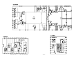
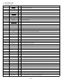
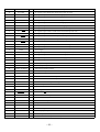
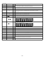
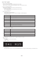
XR-DV526 U SERVICE MANUAL DVD STEREO SYSTEM BASIC TAPE MECHANISM : ZZM-3 YPR1NF BASIC DVD MECHANISM : AZG-D ZAAPA SYSTEM CD CASSEIVER SPEAKERS REMOTE CONTROLLER XR–DV526 CX–NDV526 SX–WNDV526 SX–R275 SX–C605 RC–AAS03 • This Service Manual is the “Revision Publishing” and replaces “Simple Manual” (S/M Code No. 09-007-434-1T1). S/M Code No. 09-00A-434-1R1 RE VI SIO DA N TA • If requiring information about the DVD mechanism, see Service Manual of AZG-D, (S/M Code No. 09-00A-350-6N2). SPECIFICATIONS S-VIDEO OUT Main unit CX-NDV526 <FM Tuner section> Tuning range Usable sensitivity (IHF) Antenna terminals <AM Tuner section> Tuning range Usable sensitivity Antenna 87.5 MHz to 108 MHz 13.2 dBf 75 ohms (unbalanced) VIDEO OUT Operating conditions 530 kHz to 1710 kHz (10 kHz step) 531 kHz to 1602 kHz (9 kHz step) 350 µV/m Loop antenna <General> Power requirements 120 V AC, 60 Hz Power consumption 240 W Power consumption in standby mode If the power-economizing mode is ECO OFF: 40 W If the power-economizing mode is ECO ON or ECO AUTO: 0.9 W Dimensions 260 x 326 x 345 mm (W x H x D) (101/4 x 127/8 x 135/8 in.) Weight 12.5 kg (27 lbs 9 oz.) <Amplifier section> Mid-high frequency amplifier Power output 25 W + 25 W (200 Hz – 20 kHz, THD less than 1 %, 8 ohms) Total harmonic distortion 0.1 % (15 W, 1 kHz, 8 ohms, DIN AUDIO) Low frequency amplifier Power output 75 W + 75 W (50 Hz – 200 Hz, THD less than 1 %, 6 ohms) Total harmonic distortion 0.1 % (40 W, 130 Hz, 6 ohms, DIN AUDIO) Rear (Surround) 25 W + 25 W (1 kHz, THD less than 1 %, 8 ohms) Center 25 W (1 kHz, THD less than 1 %, 8 ohms) Inputs VIDEO/AUX: 300 mV (adjustable) MIC: 1.0 mV (10 k ohms) Outputs SPEAKERS HIGH FREQ: accept speakers of 8 ohms or more SPEAKERS LOW FREQ: accept speakers of 6 ohms or more SURROUND SPEAKERS: accept speakers of 8 ohms to 16 ohms CENTER SPEAKER: accept speakers of 8 ohms or more SUB WOORER: 1.1 V DIGITAL AUDIO OUT (OPTICAL) PHONES (stereo jack): accepts headphones of 32 ohms or more <Cassette deck section> Track format Frequency response Recording system Heads <Disc player section> Laser D/A converter Signal-to-noise ratio Harmonic distortion Signal format Supported discs Y output: 1 Vp-p (75 ohms, sync negative) C output: 0.286 Vp-p Video composit output 1 Vp-p (75 ohms, sync negative) One RCA jack 5 °C to 35 °C (41 °F to 95 °F) Speaker system SX-WNDV526 Speaker system Speaker units Impedance Sensitivity Dimensions (W x H x D) Weight 3 way, Built-in subwoofer (magnetic shielded type) Subwoofer: 160 mm (63/8 in.) cone type Full range: 100 mm (4 in.) cone type Super tweeter: 20 mm (13/16 in.) ceramic type 6 ohms/8 ohms 87 dB/W/m 240 x 324 x 270 mm (91/2 x 127/8 x 103/4 in.) 4.8 kg (10 lbs 9 oz.) • Design and specifications are subject to change without notice. • The word "BBE"and the "BBE symbol" are trademarks of BBE Sound, Inc. Under license from BBE Sound,Inc. • Manufactured under license from Dolby Laboratories Licensing Corporation. "DOLBY", the double-D symbol and "PRO LOGIC" are trademarks of Dolby Laboratories Licensing Corporation. 4 tracks, 2 channels stereo 50 Hz – 15000 Hz AC bias DECK 1: Playback head x 1 DECK 2: Recording/playback head x 1, erase head x 1 • Manufactured under license from Digital Theater Systems, Inc. US Pat. No. 5,451,942 and other worldwide patents issued and pending. "DTS" and "DTS Digital Surround" are trademarks of Digital Theater Systems, Inc. C1996 Digital Theater systems, Inc. All rights reserved. Semiconductor laser (λ =780 nm) 1 bit dual 85 dB (1 kHz, 0 dB) 0.05 % (1 kHz, 0 dB) NTSC DVD video discs 12 cm (single-sided single-layer, singlesided double-layer, double-sided-double layer) 8 cm (single-sided single-layer, singlesided double-layer, double-sided-double layer) Compact discs (CD-DA, CD-R, CD-RW, video CD) 12 cm and 8 cm discs –2– PROTECTION OF EYES FROM LASER BEAM DURING SERVICING This set employs laser. Therefore, be sure to follow carefully the CAUTION instructions below when servicing. Use of controls or adjustments or performance of procedures other than those specified herin may result in hazardous radiation exposure. WARNING!! WHEN SERVICING, DO NOT APPROACH THE LASER EXIT WITH THE EYE TOO CLOSELY. IN CASE IT IS NECESSARY TO CONFIRM LASER BEAM EMISSION. BE SURE TO OBSERVE FROM A DISTANCE OF MORE THAN 30cm FROM THE SURFACE OF THE OBJECTIVE LENS ON THE OPTICAL PICK-UP BLOCK. ATTENTION L’utillisation de commandes, réglages ou procédures autres que ceux spécifiés peut entraîner une dangereuse exposition aux radiations. ADVARSEL Usynlig laserståling ved åbning, når sikkerhedsafbrydereer ude af funktion. Undgå udsættelse for stråling. Caution: Invisible laser radiation when open and interlocks defeated avoid exposure to beam. Advarsel: Usynlig laserståling ved åbning, når sikkerhedsafbrydere er ude af funktion. Undgå udsættelse for stråling. This Compact Disc player is classified as a CLASS 1 LASER product. The CLASS 1 LASER PRODUCT label is located on the rear exterior. VAROITUS! Laiteen Käyttäminen muulla kuin tässä käyttöohjeessa mainitulla tavalla saataa altistaa käyt-täjän turvallisuusluokan 1 ylittävälle näkymättömälle lasersäteilylle. CLASS 1 KLASSE 1 LUOKAN 1 KLASS 1 VARNING! Om apparaten används på annat sätt än vad som specificeras i denna bruksanvising, kan användaren utsättas för osynling laserstrålning, som överskrider gränsen för laserklass 1. LASER PRODUCT LASER PRODUKT LASER LAITE LASER APPARAT Precaution to replace Optical block (SF – HD3AV) PICKUP Assy PWB Solder short land for DVD laser diode Body or clothes electrostatic potential could ruin laser diode in the optical block. Be sure ground body and workbench, and use care the clothes do not touch the diode. 1) After the connection, remove solder shown in the right figure. –3– Solder short land for CD laser diode NOTE ON BEFORE STARTING REPAIR 1. Forced discharge of electrolytic capacitor of power supply block When repair is going to be attempted in the set that uses relay circuit in the power supply block, electric potential is kept charged across the electrolytic capacitors (C101, 102) even though AC power cord is removed. If repair is attempted in this condition, secondary defect can occur. In order to prevent the secondary trouble, perform the following measures before starting repair work. Discharge procedure MAIN C.B 1 Remove the AC power cord. 2 Connect a discharging resistor at an end of lead wire that has clips at both ends. Connect the other end of the lead wire to metal chassis. 3 Contact the other end of the discharging resistor to the positive (+) side (+VH) of C101. (For two seconds) 4 Contact the same end of the discharging resistor as step 3 to the negative (-) side (-VH) of C102 in the same way. (For two seconds) 5 Check that voltage across C101 and C102 has decreased to 1 V or less using a multimeter or an oscilloscope. D101 3 2 Select a discharging resistor referring to the following table. C102 4 2 Fig-1 Charging voltage (V) Discharging (C101, 102) resistor (Ω) 25-48 100 3 87-A00-247-090 49-140 220 5 87-A00-232-090 Rated power (W) C101 Parts number Note: The reference numbers (C101, C102) of the electrolytic capacitors can change depending on the models. Be sure to check the reference numbers of the charging capacitors on schematic diagram before starting the discharging work. 2. Check items before exchanging the MICROCOMPUTER Be sure to check the following items before exchanging the MICROCOMPUTER. Exchange the MICROCOMPUTER after confirming that the MICROCOMPUTER is surely defective. 2-1. Regarding the HOLD terminal of the MICROCOMPUTER When the HOLD terminal (INPUT) of the MICROCOMPUTER is “H”, the MICROCOMPUTER is judged to be operating correctly. When this terminal is “L”, the main power cannot be turned on. Therefore, be sure to check the terminal voltage of the HOLD terminal before exchange. When the MICROCOMPUTER is not defective, the HOLD terminal can also go “L” when the POWER AMPLIFIER has any abnormalities that triggers the abnormality detection circuit on the MAIN C. B. that sets the HOLD terminal to “L”. • Good or no good judgement of the MICROCOMPUTER 1 Turn on the AC main power. 2 Confirm that the main power is turned on and the HOLD terminal of the MICROCOMPUTER keeps the “H” level or not. 3 When the HOLD terminal is “L” level, the abnormality detection circuit is judged to be working correctly and the MICROCOMPUTER is judged to be good. –4– In such a case, check also if the POWER AMPLIFIER circuit or power supply circuit has any abnormalities or not. 2-2. Regarding reset TE R There are cases that the machine does not work correctly because the MICROCOMPUTER is not reset even though the AC power cord is re-inserted, or the software reset (pressing the STOP key + POWER key) is performed. When the above described phenomenon occurs, it can lead to wrong judgement as if the MICROCOMPUTER is defective and to exchange the MICROCOMPUTER. In such a case, perform the forced-reset by the following procedure and check good or no good of the MICROCOMPUTER. 1 Remove the AC power cord. M IC RO CO M PU FRONT C.B 18 15 C113 % VSS MICROC113 COMPUTER * VDD FRONT C.B Short with tweezers. Fig-2-2 2 Short both ends of the electrolytic capacitor C113 that is connected to VDD of the MICROCOMPUTER with tweezers. 3 Connect the AC power cord again. If the MICROCOMPUTER returns to the normal operation, the MICROCOMPUTER is good. Note: The reference number or MICROCOMPUTER pin number of transistor (Q110) and electrolytic capacitor (C113) can change depending on the models. Be sure to check the reference numbers on schematic diagram before starting the discharging work. 2-3. Confirmation of soldering state of MICROCOMPUTER Check the soldering state of the MICROCOMPUTER in addition to the above described procedures. Be sure to exchange the MICROCOMPUTER after surely confirming that the trouble is not caused by poor soldering but the MICROCOMPUTER itself. –5– ELECTRICAL MAIN PARTS LIST REF. NO. PART NO. KANRI NO. DESCRIPTION REF. NO. PART NO. IC 87-A21-269-010 87-A21-396-010 87-A21-398-010 8A-DJV-610-030 87-A21-629-010 IC,EW732 IC,STK490-040 IC,STK490-110 C-IC,LC87F65C8G-SAN1 IC,SPS-442-1-N 87-A20-783-040 87-A21-097-040 87-A21-015-040 87-A21-577-040 87-A21-452-030 C-IC,BA7762AFS C-IC,M62463AFP C-IC,M62491FP C-IC,M61506FP C-IC,BD3876KS2 87-070-289-040 87-A21-560-010 87-070-127-110 C-IC,BU2092F IC,LA1844L-A IC,LC72131 D TRANSISTOR 87-026-245-080 87-026-609-080 87-A30-198-080 87-026-610-080 87-A30-076-080 TR,DTC114ES TR,KTA1266GR TR,KTC3199GR TR,KTC3198GR C-TR,2SC3052F 87-A30-075-080 87-A30-318-080 89-213-702-010 87-026-210-040 87-A30-107-070 C-TR,2SA1235F TR,CSA952K TR,2SB1370E C-TR,DTC144EK C-TR,CMBT5401 87-A30-269-040 87-A30-106-040 87-A30-190-080 87-A30-087-080 87-A30-256-010 C-FET,2SJ461-T1 C-TR,CMBT5551 TR,CC5551 C-FET,2SK2158 TR,2SD1933 87-A30-255-010 87-A30-074-080 87-A30-495-080 87-A30-329-080 87-A30-073-080 TR,2SB1342 C-TR,RT1P 141C TR,2SA1981Y TR,CD1585BC C-TR,RT1N141C 87-A30-105-080 87-A30-086-040 87-A30-202-080 89-327-143-080 87-A30-072-080 C-TR,RT1P 441C C-TR,CSD1306E C-TR,RT1P441C C-TR,2SC2714O C-TR,RT1P 144C 87-A30-234-080 TR,CSC4115BC DIODE C3 C4 C21 C22 C25 C26 C27 87-016-658-000 87-016-658-000 87-010-406-080 87-010-406-080 87-010-406-080 C28 C31 C32 C33 C34 87-010-406-080 87-010-263-080 87-010-197-080 87-010-263-080 87-010-260-080 CAP,ELECT 22-50 CAP,ELECT 100-10V CAP,CHIP 0.01 DM CAP,ELECT 100-10V CAP,ELECT 47-25V C35 C36 C38 C39 C40 87-010-380-080 87-010-381-080 87-010-409-080 87-010-409-080 87-010-197-080 CAP,ELECT 47-16V CAP,ELECT 330-16V CAP,E 220-50 SME CAP,E 220-50 SME CAP,CHIP 0.01 DM C60 C80 C81 C82 C104 87-010-403-080 87-010-401-080 87-010-383-080 87-010-260-080 87-010-196-080 CAP,ELECT 3.3-50V CAP,ELECT 1-50V CAP,ELECT 33-25V CAP,ELECT 47-25V CHIP CAPACITOR,0.1-25 C105 C111 C112 C113 C114 87-010-196-080 87-010-545-080 87-010-545-080 87-010-545-080 87-010-545-080 CHIP CAPACITOR,0.1-25 CAP,ELECT 0.22-50V CAP,ELECT 0.22-50V CAP,ELECT 0.22-50V CAP,ELECT 0.22-50V C115 C116 C121 C122 C163 87-010-546-080 87-010-546-080 87-010-546-080 87-010-546-080 87-010-196-080 CAP,ELECT 0.33-50V CAP,ELECT 0.33-50V CAP,ELECT 0.33-50V CAP,ELECT 0.33-50V CHIP CAPACITOR,0.1-25 C171 C172 C173 C174 C301 87-012-368-080 87-012-368-080 87-012-368-080 87-012-368-080 87-010-318-080 C-CAP,S C-CAP,S C-CAP,S C-CAP,S C-CAP,S 0.1-50 0.1-50 0.1-50 0.1-50 47P-50 C302 C303 C304 C305 C306 87-010-318-080 87-012-157-080 87-012-157-080 87-012-157-080 87-012-157-080 C-CAP,S C-CAP,S C-CAP,S C-CAP,S C-CAP,S 47P-50 CH 330P-50 CH 330P-50 CH 330P-50 CH 330P-50 CH C307 C309 C310 C311 C312 87-010-196-080 87-010-196-080 87-010-196-080 87-010-198-080 87-010-198-080 CHIP CAPACITOR,0.1-25 CHIP CAPACITOR,0.1-25 CHIP CAPACITOR,0.1-25 CAP,CHIP 0.022 CAP,CHIP 0.022 C313 C314 C315 C316 C321 87-010-180-080 87-010-180-080 87-010-182-080 87-010-182-080 87-012-142-080 C-CAP,S 1500P C-CAP,S 1500P C-CAP,S 2200P-50 B C-CAP,S 2200P-50 B CAP,S 0.33-16 C322 C324 C325 C327 C328 87-012-142-080 87-010-260-080 87-010-370-080 87-010-404-080 87-010-404-080 CAP,S 0.33-16 CAP,ELECT 47-25V CAP,E 330-6.3 SME CAP,ELECT 4.7-50V CAP,ELECT 4.7-50V C332 C335 C336 C337 C339 87-010-196-080 87-010-401-080 87-010-401-080 87-010-196-080 87-010-196-080 CHIP CAPACITOR,0.1-25 CAP,ELECT 1-50V CAP,ELECT 1-50V CHIP CAPACITOR,0.1-25 CHIP CAPACITOR,0.1-25 87-010-196-080 87-012-140-080 87-012-140-080 87-010-175-080 87-010-178-080 CHIP CAPACITOR,0.1-25 C-CAP,S 470P C-CAP,S 470P C-CAP,S 560P CHIP CAP,S 1000P 87-010-260-080 87-010-197-080 87-010-183-080 87-010-183-080 87-010-183-080 CAP,ELECT 47-25V CAP,CHIP 0.01 DM C-CAP,S 2700P-50 B C-CAP,S 2700P-50 B C-CAP,S 2700P-50 B 87-A40-839-090 87-A40-224-010 87-020-465-080 87-A40-553-080 87-A40-776-080 DIODE,G5SBA60L-6088 DIODE,GBU8DL DIODE,1SS133 DIODE,1N4003 LES ZENER,UZ27BSD 87-A40-764-080 87-A40-313-080 87-A40-270-080 87-A40-269-080 87-A40-768-080 ZENER,UZ10BSC C-DIODE,MC2840 C-DIODE,MC2838 C-DIODE,MC2836 ZENER,UZ16BSA 87-017-495-080 87-A40-754-080 87-A40-752-080 87-A40-760-080 87-A40-747-080 DIODE,1N5393 ZENER,UZ6.8BSC ZENER,UZ6.2BSC ZENER,UZ9.1BSA ZENER,UZ5.1BSB 87-A40-802-080 87-A40-745-080 87-017-149-080 ZENER,UZ5.1BSC ZENER,UZ4.7BSA ZENER,HZS6A2L C340 C351 C352 C354 C355 C-CAP,S 0.1-50 F C-CAP,S 0.1-50 F C356 C357 C358 C359 C360 MAIN C.B 87-012-368-080 87-012-368-080 –6– KANRI DESCRIPTION NO. CAP,E 4700-35 M SMG CAP,E 4700-35 M SMG CAP,ELECT 22-50 CAP,ELECT 22-50 CAP,ELECT 22-50 F F F F CH REF. NO. PART NO. C370 C373 C374 C378 C379 87-010-196-080 87-A11-177-080 87-A11-177-080 87-010-196-080 87-010-382-080 KANRI DESCRIPTION NO. CHIP CAPACITOR,0.1-25 C-CAP,S 0.15-16 K B C-CAP,S 0.15-16 K B CHIP CAPACITOR,0.1-25 CAP,ELECT 22-25V REF. NO. PART NO. C380 C386 C388 C391 C392 87-010-382-080 87-010-196-080 87-012-156-080 87-010-319-080 87-010-319-080 CAP,ELECT 22-25V CHIP CAPACITOR,0.1-25 C-CAP,S 220P-50 CH C-CAP,S 56P-50 CH C-CAP,S 56P-50 CH C476 C477 C478 C479 C480 87-012-140-080 87-012-140-080 87-010-401-080 87-010-179-080 87-010-179-080 C-CAP,S 470P C-CAP,S 470P CAP,ELECT 1-50V C-CAP,S 1200P C-CAP,S 1200P C393 C394 C401 C402 C403 87-010-319-080 87-010-319-080 87-010-176-080 87-010-176-080 87-010-958-080 C-CAP,S 56P-50 CH C-CAP,S 56P-50 CH C-CAP,S 680P-50 SL C-CAP,S 680P-50 SL CHIP-CAP,S 0.01-25BJ C481 C482 C489 C491 C492 87-010-179-080 87-010-179-080 87-010-402-080 87-010-402-080 87-010-402-080 C-CAP,S 1200P C-CAP,S 1200P CAP,ELECT 2.2-50V CAP,ELECT 2.2-50V CAP,ELECT 2.2-50V C404 C405 C406 C407 C408 87-010-958-080 87-010-958-080 87-010-958-080 87-010-401-080 87-010-401-080 CHIP-CAP,S 0.01-25BJ CHIP-CAP,S 0.01-25BJ CHIP-CAP,S 0.01-25BJ CAP,ELECT 1-50V CAP,ELECT 1-50V C531 C532 C533 C534 C535 87-010-405-080 87-010-196-080 87-010-196-080 87-012-156-080 87-010-178-080 CAP,ELECT 10-50V CHIP CAPACITOR,0.1-25 CHIP CAPACITOR,0.1-25 C-CAP,S 220P-50 CH CHIP CAP,1000P C409 C410 C411 C412 C413 87-010-196-080 87-010-384-080 87-010-400-080 87-010-400-080 87-010-400-080 CHIP CAPACITOR,0.1-25 CAP,ELECT 100-25V CAP,ELECT 0.47-50V CAP,ELECT 0.47-50V CAP,ELECT 0.47-50V C536 C541 C609 C610 C611 87-010-196-080 87-010-178-080 87-010-181-080 87-010-181-080 87-010-598-080 CHIP CAPACITOR,0.1-25 CHIP CAP,1000P CAP,CHIP S 1800P CAP,CHIP S 1800P C-CAP,S 0.068-16 K R GRM C414 C415 C416 C417 C418 87-010-401-080 87-010-546-080 87-010-546-080 87-010-221-080 87-A10-891-080 CAP,ELECT 1-50V CAP,ELECT 0.33-50V CAP ELECT 0.33-50V CAP,ELECT 470-10V CAP,E 4.7-25 SME(K) C612 C613 C614 C616 C617 87-010-369-080 87-010-197-080 87-016-081-080 87-010-184-080 87-010-194-080 C-CAP,S 0.033-25 K B CAP,CHIP 0.01 DM C-CAP,S 0.1-16 RK CHIP CAPACITOR,3300P CAP,CHIP 0.047 C419 C420 C421 C422 C424 87-A10-800-080 87-010-374-080 87-010-196-080 87-A10-804-080 87-010-374-080 C-CAP,S 6800P-16 J B CM CAP,ELECT 47-10V CHIP CAPACITOR,0.1-25 C-CAP,S 0.1-25 J B CAP,ELECT 47-10V C618 C619 C620 C621 C623 87-010-401-080 87-010-263-080 87-016-081-080 87-010-197-080 87-010-401-080 CAP,ELECT 1-50V CAP,ELECT 100-10V C-CAP,S 0.1-16 RK CAP,CHIP 0.01 DM CAP,ELECT 1-50V C425 C429 C430 C431 C432 87-010-196-080 87-010-544-080 87-A10-201-080 87-010-971-080 87-012-349-080 CHIP CAPACITOR,0.1-25 CAP,ELECT 0.1-50V C-CAP,S 0.33-16 K B C-CAP,S 4700P-50 B J C-CAP,S 1000P-50 CH C624 C626 C627 C628 C629 87-010-401-080 87-010-596-080 87-010-400-080 87-010-400-080 87-010-596-080 CAP,ELECT 1-50V C-CAP,S 0.047-16 CAP,ELECT 0.47-50V CAP,ELECT 0.47-50V CAP,S 0.047-16 C433 C434 C435 C436 C437 87-A11-183-080 87-A11-182-080 87-A11-182-080 87-A11-183-080 87-010-971-080 C-CAP,S C-CAP,S C-CAP,S C-CAP,S C-CAP,S C630 C631 C632 C633 C634 87-010-263-080 87-010-185-080 87-010-185-080 87-010-178-080 87-010-196-080 CAP,ELECT 100-10V C-CAP,S 3900P-50 B C-CAP,S 3900P-50 B CHIP CAP,1000P CHIP CAPACITOR,0.1-25 C438 C439 C440 C441 C442 87-012-349-080 87-010-805-080 87-010-401-080 87-A10-799-080 87-A10-802-080 C-CAP,S 1000P-50 CH CAP,S 1-16 CAP,ELECT 1-50V C-CAP,S 5600P-16 J B CM C-CAP,S 0.047-16 J B CM C635 C636 C637 C638 C639 87-A10-307-080 87-A10-307-080 87-A10-307-080 87-A10-307-080 87-010-405-080 CAP,M 0.1-50 J CAP,M 0.1-50 J CAP,M 0.1-50 J CAP,M 0.1-50 J CAP,ELECT 10-50V C443 C444 C445 C446 C447 87-A10-229-080 87-012-393-080 87-012-393-080 87-010-404-080 87-010-404-080 C-CAP,S 0.68-10 K W5R C-CAP,S 0.22-16 R K C-CAP,S 0.22-16 R K CAP,ELECT 4.7-50V CAP,ELECT 4.7-50V C643 C644 C645 C671 C672 87-010-196-080 87-010-401-080 87-010-322-080 87-010-322-080 87-010-322-080 CHIP CAPACITOR,0.1-25 CAP,ELECT 1-50V C-CAP,S 100P-50 CH C-CAP,S 100P-50 CH C-CAP,S 100P-50 CH C448 C449 C450 C451 C452 87-012-393-080 87-012-393-080 87-016-081-080 87-A10-802-080 87-A10-802-080 C-CAP,S C-CAP,S C-CAP,S C-CAP,S C-CAP,S 0.22-16 R K 0.22-16 R K 0.1-16 RK 0.047-16 J B CM 0.047-16 J B CM C673 C676 C679 C680 C682 87-010-197-080 87-010-382-080 87-010-196-080 87-010-190-080 87-010-196-080 CAP,CHIP 0.01 DM CAP,ELECT 22-25V CHIP CAPACITOR,0.1-25 CHIP-CAP,S 0.01 CHIP CAPACITOR,0.1-25 C453 C454 C455 C456 C457 87-016-081-080 87-016-081-080 87-A10-801-080 87-A10-801-080 87-016-081-080 C-CAP,S C-CAP,S C-CAP,S C-CAP,S C-CAP,S 0.1-16 RK 0.1-16 RK 0.022-16 J B CM 0.022-16 J B CM 0.1-16 RK C685 C771 C772 C779 C780 87-010-190-080 87-010-263-080 87-010-197-080 87-010-426-080 87-010-426-080 CHIP-CAP,S 0.01 CAP,ELECT 100-10V CAP,CHIP 0.01 DM C-CAP,S 0.012-25 B C-CAP,S 0.012-25 B C461 C463 C465 C466 C467 87-010-196-080 87-010-196-080 87-016-669-080 87-010-194-080 87-A10-201-080 CHIP CAPACITOR,0.1-25 CHIP CAPACITOR,0.1-25 C-CAP,S 0.1-25 CAP,CHIP 0.047 C-CAP,S 0.33-16 K B C782 C783 C784 C785 C786 87-010-197-080 87-010-197-080 87-010-197-080 87-010-197-080 87-010-197-080 CAP,CHIP CAP,CHIP CAP,CHIP CAP,CHIP CAP,CHIP 0.12-16 J B 0.27-16 J B 0.27-16 J B 0.12-16 J B 4700P-50 B J –7– C468 C472 C473 C474 C475 87-A10-060-080 87-012-140-080 87-012-140-080 87-012-140-080 87-012-140-080 KANRI NO. C-CAP,S C-CAP,S C-CAP,S C-CAP,S C-CAP,S DESCRIPTION 0.18-16 K B 470P 470P 470P 470P 0.01 0.01 0.01 0.01 0.01 DM DM DM DM DM REF. NO. PART NO. C788 C789 C790 C791 C792 87-010-149-080 87-A10-592-080 87-A10-592-080 87-010-196-080 87-010-197-080 KANRI DESCRIPTION NO. C-CAP,S 5P-50 CH C-CAP,S 0.015-50 J B C-CAP,S 0.015-50 J B CHIP CAPACITOR,0.1-25 CAP,CHIP 0.01 DM C793 C795 C796 C797 C798 87-010-404-080 87-010-197-080 87-010-197-080 87-010-405-080 87-010-197-080 CAP,ELECT 4.7-50V CAP,CHIP 0.01 DM CAP,CHIP 0.01 DM CAP,ELECT 10-50V CAP,CHIP 0.01 DM CN611 CNA1 CNA2 FFC431 FFC610 87-049-919-010 8A-NF8-653-010 8A-NF6-630-110 88-911-351-110 8A-DJV-621-010 CONN,3P EH V WHT CONN ASSY,9P TID-A(480) CONN ASSY,3P(VM) ANF-6 FF-CABLE,11P 1.25 350MM FF-CABLE,5P 1.0 270MM C799 C800 C801 C802 C803 87-010-407-080 87-010-194-080 87-010-403-080 87-010-194-080 87-010-198-080 CAP,ELECT 33-50V CAP,CHIP 0.047 CAP,ELECT 3.3-50V CAP,CHIP 0.047 CAP,CHIP 0.022 FFE831 J102 J103 J604 J831 A8-8ZA-193-070 87-033-229-010 87-A60-483-010 87-A60-881-010 87-A61-456-010 8ZA-1 YFEUNC TERMINAL,SPKR 4P YKD21-0242 JACK,DIA6.3 BLK ST W/S KM JACK,PIN 2P MSP 242V05 PBSN TERMINAL,ANT 4P MSP-154V-02 PB C804 C807 C808 C809 C810 87-010-263-080 87-010-400-080 87-010-401-080 87-010-401-080 87-010-196-080 CAP,ELECT 100-10V CAP,ELECT 0.47-50V CAP,ELECT 1-50V CAP,ELECT 1-50V CHIP CAPACITOR,0.1-25 L101 L102 L301 L302 L351 87-A50-610-010 87-A50-610-010 87-A50-625-010 87-A50-625-010 87-007-342-010 COIL,1UH K(MDEC) COIL,1UH K(MDEC) COIL,TRAP 85KHZ(SANWA) COIL,TRAP 85KHZ(SANWA) COIL,OSC 85KHZ BIAS C811 C812 C814 C815 C816 87-010-403-080 87-010-403-080 87-010-197-080 87-010-400-080 87-010-400-080 CAP,ELECT 3.3-50V CAP,ELECT 3.3-50V CAP,CHIP 0.01 DM CAP,ELECT 0.47-50V CAP,ELECT 0.47-50V L801 L802 L811 L832 L951 87-A50-608-010 87-A91-551-010 87-005-847-080 87-005-847-080 8A-NF8-667-010 COIL,FM DET-N(TOK) FLTR,PCFJZH-450 L(TOK) COIL,2.2UHK CECS COIL,2.2UHK CECS COIL,AM PACK 4(TOK) C821 C823 C824 C825 C842 87-010-405-080 87-010-177-080 87-010-404-080 87-010-596-080 87-010-197-080 CAP,ELECT 10-50V C-CAP,S 820P-50 SL CAP,ELECT 4.7-50V CAP,S 0.047-16 CAP,CHIP 0.01 DM R161 R162 R163 R164 R407 87-A00-439-050 87-A00-439-050 87-A00-439-050 87-A00-439-050 87-022-214-080 RES,180-1/2W J RP RES,180-1/2W J RP RES,180-1/2W J RP RES,180-1/2W J RP C-RES S100K-1/10W F C843 C844 C845 C846 C847 87-010-197-080 87-010-197-080 87-010-197-080 87-010-197-080 87-010-197-080 CAP,CHIP CAP,CHIP CAP,CHIP CAP,CHIP CAP,CHIP DM DM DM DM DM R790 R991 R993 R995 SFR351 87-010-197-080 87-010-322-080 87-010-322-080 87-010-322-080 87-A90-433-080 CAP,CHIP 0.01 DM C-CAP,S 100P-50 CH C-CAP,S 100P-50 CH C-CAP,S 100P-50 CH SFR,50K H NVZ6TLTA C848 C849 C850 C851 C852 87-010-197-080 87-010-197-080 87-010-260-080 87-010-197-080 87-010-197-080 CAP,CHIP 0.01 DM CAP,CHIP 0.01 DM CAP,ELECT 47-25V CAP,CHIP 0.01 DM CAP,CHIP 0.01 DM SFR352 WH1 X991 87-A90-433-080 87-A90-510-010 87-A70-061-010 SFR,50K H NVZ6TLTA HLDR,WIRE 2.5-9P VIB,XTAL 4.500MHZ CSA-309 C853 C858 C859 C860 C959 87-010-197-080 87-010-196-080 87-010-196-080 87-010-197-080 87-010-196-080 CAP,CHIP 0.01 DM CHIP CAPACITOR,0.1-25 CHIP CAPACITOR,0.1-25 CAP,CHIP 0.01 DM CHIP CAPACITOR,0.1-25 C201 C202 C203 C204 C205 87-010-322-080 87-010-322-080 87-010-322-080 87-010-322-080 87-010-322-080 C-CAP,S C-CAP,S C-CAP,S C-CAP,S C-CAP,S 100P-50 100P-50 100P-50 100P-50 100P-50 CH CH CH CH CH C960 C961 C963 C971 C972 87-010-196-080 87-010-152-080 87-015-785-080 87-010-381-080 87-010-404-080 CHIP CAPACITOR,0.1-25 C-CAP,S 8P-50 CH CHIP CAPACITOR,0.1-25 Z F CAP,ELECT 330-16V CAP,ELECT 4.7-50V C206 C207 C208 C209 C210 87-010-322-080 87-010-322-080 87-010-322-080 87-010-322-080 87-010-322-080 C-CAP,S C-CAP,S C-CAP,S C-CAP,S C-CAP,S 100P-50 100P-50 100P-50 100P-50 100P-50 CH CH CH CH CH C973 C974 C979 C981 C982 87-010-197-080 87-010-197-080 87-010-322-080 87-010-260-080 87-010-196-080 CAP,CHIP 0.01 DM CAP,CHIP 0.01 DM C-CAP,S 100P-50 CH CAP,ELECT 47-25V CHIP CAPACITOR,0.1-25 C211 C251 C253 C254 C255 87-010-322-080 87-010-405-040 87-010-196-080 87-012-369-080 87-010-560-040 C-CAP,S 100P-50 CH CAP,E 10-50 CHIP CAPACITOR,0.1-25 C-CAP,S 0.047-50F CAP,E 10-50 GAS C983 C984 C987 C991 C992 87-010-197-080 87-010-197-080 87-010-197-080 87-010-312-080 87-010-312-080 CAP,CHIP 0.01 DM CAP,CHIP 0.01 DM CAP,CHIP 0.01 DM C-CAP,S 15P-50 CH C-CAP,S 15P-50 CH C256 C259 C264 C270 C271 87-010-405-040 87-010-405-040 87-010-196-080 87-010-178-080 87-010-178-080 CAP,E 10-50 CAP,E 10-50 CHIP CAPACITOR,0.1-25 CHIP CAP,1000P CHIP CAP,1000P C993 C995 C997 C998 C999 87-010-178-080 87-010-178-080 87-010-196-080 87-010-260-080 87-A11-155-080 CHIP CAP,1000P CHIP CAP,1000P CHIP CAPACITOR,0.1-25 CAP,ELECT 47-25V CAP,TC U 0.01-16 Z F C273 C274 C301 C302 C303 87-010-178-080 87-010-178-080 87-010-182-080 87-010-196-080 87-010-196-080 CHIP CAP,1000P CHIP CAP,1000P C-CAP,S 2200P-50 B CHIP CAPACITOR,0.1-25 CHIP CAPACITOR,0.1-25 CF831 CF832 CN1 CN91 CN101 87-008-261-010 87-008-261-010 87-A60-996-010 87-A60-109-010 87-A60-996-010 FILTER,SFE10.7MA5 FILTER,SFE10.7MA5 CONN,13P V BLK TAC-L13X-A3 CONN,2P V S2M-2W CONN,13P V BLK TAC-L13X-A3 C312 C314 C315 C316 87-010-498-040 87-010-196-080 87-010-196-080 87-010-196-080 CAP,E 10-16 GAS CHIP CAPACITOR,0.1-25 CHIP CAPACITOR,0.1-25 CHIP CAPACITOR,0.1-25 0.01 0.01 0.01 0.01 0.01 REF. NO. PART NO. CN301 CN351 CN431 CN601 CN610 87-099-827-010 87-099-832-010 87-099-013-010 87-099-719-010 87-A61-171-010 KANRI DESCRIPTION NO. CONN,3P S2M-3W CONN,8P S2M-8W CONN,11P 6216 V CONN,30P TYK-B(X) CONN,5P V GRY FMN-BTK FRONT C.B –8– REF. NO. PART NO. S427 S428 S429 S430 S431 87-A91-024-180 87-A91-024-180 87-A91-024-180 87-A91-024-180 87-A91-024-180 KANRI NO. SW,TACT SW,TACT SW,TACT SW,TACT SW,TACT C-CAP,S 15P-50 CH C-CAP,180P-50CH C-CAP,S 100P-50 CH C-CAP,S 220P-50 CH CAP,CHIP 0.01 DM S432 S433 S434 S435 SW252 87-A91-024-180 87-A91-024-180 87-A91-024-180 87-A91-024-180 87-A91-555-010 SW,TACT SW,TACT SW,TACT SW,TACT SW,RTRY 87-010-194-080 87-010-382-040 87-010-197-080 87-010-196-080 87-010-196-080 CAP,CHIP 0.047 CAP,E 22-25 SME CAP,CHIP 0.01 DM CHIP CAPACITOR,0.1-25 CHIP CAPACITOR,0.1-25 SW253 87-A91-542-010 SW,RTRY EC12E12504 C453 C454 C455 C458 C459 87-010-196-080 87-010-198-080 87-010-198-080 87-010-320-080 87-010-320-080 CHIP CAPACITOR,0.1-25 CAP,CHIP 0.022 CAP,CHIP 0.022 CHIP CAP,68P CHIP CAP,68P C101 C102 C103 C104 C107 87-010-181-080 87-010-181-080 87-010-545-080 87-010-545-080 87-010-405-080 CAP,CHIP S 1800P CAP,CHIP S 1800P CAP,ELECT 0.22-50V CAP,ELECT 0.22-50V CAP,ELECT 10-50V C502 C503 C504 C505 C506 87-010-186-080 87-010-112-040 87-010-405-040 87-010-545-040 87-010-320-080 CAP,CHIP 4700P CAP,E 100-16 CAP,E 10-50 CAP,E 0.22-50 SME CHIP CAP,68P C108 C111 C112 C113 C114 87-010-405-080 87-010-179-080 87-010-179-080 87-010-405-080 87-010-405-080 CAP,ELECT 10-50V CAP,CHIP S 1200P CAP,CHIP S 1200P CAP,ELECT 10-50V CAP,ELECT 10-50V C513 C515 C602 C603 C604 87-010-196-080 87-010-178-080 87-010-322-080 87-010-322-080 87-010-322-080 CHIP CAPACITOR,0.1-25 CHIP CAP,1000P C-CAP,S 100P-50 CH C-CAP,S 100P-50 CH C-CAP,S 100P-50 CH C115 C116 C119 C120 C133 87-A12-180-080 87-A12-180-080 87-010-197-080 87-010-197-080 87-010-190-080 CAP,E 10-63 M 105 KME CAP,E 10-63 M 105 KME CAP,CHIP 0.01 DM CAP,CHIP 0.01 DM CHIP-CAP,S 0.01-50 C650 C699 CN101 CN102 CN302 87-010-196-080 87-010-196-080 87-099-720-010 87-A61-356-010 87-A60-136-010 CHIP CAPACITOR,0.1-25 CHIP CAPACITOR,0.1-25 CONN,30P TYK-B(P) CONN,13P V GRY FMN-BTK CONN,11P V FE C153 C201 C202 C203 C204 87-010-188-080 87-A10-300-080 87-A10-300-080 87-A10-300-080 87-A10-300-080 CAP,CHIP 6800P CAP,M 0.027-50 CAP,M 0.027-50 CAP,M 0.027-50 CAP,M 0.027-50 FB301 FB501 FFC102 FFC302 FL401 87-008-372-080 87-008-372-080 8A-DJV-620-010 88-911-101-110 8A-DJV-601-010 FILTER,EMI BL01 RN1 FILTER,EMI BL01 RN1 FF-CABLE,13P 1.0 300MM FF-CABLE,11P 1.25 FL,HNA-11MM34(ADJ-28) C205 C206 C207 C208 C209 87-010-180-080 87-010-180-080 87-010-401-080 87-010-401-080 87-010-187-080 C-CAP,S 1500P C-CAP,S 1500P CAP,ELECT 1-50V CAP,ELECT 1-50V CAP,CHIP S 5600P J501 L331 LED311 LED601 LED602 87-A61-242-010 87-A50-333-010 87-A40-589-040 87-A40-803-010 87-A40-619-080 JACK,6.3 BLK MONO W/SW V KM COIL,OSC 9.43MHZ LED,SLR-56VCT31 RED LED,SELU1E10CXM-S LF38 BLUE LED,SLR-56PT-TE7-W GRN C210 C211 C212 C215 C216 87-010-187-080 87-010-403-080 87-010-403-080 87-010-179-080 87-010-179-080 CAP,CHIP S 5600P CAP,ELECT 3.3-50V CAP,ELECT 3.3-50V CAP,CHIP S 1200P CAP,CHIP S 1200P LED603 LED605 LED607 LED608 S401 87-A40-619-080 87-A40-619-080 87-A40-619-080 87-A40-619-080 87-A91-024-180 LED,SLR-56PT-TE7-W LED,SLR-56PT-TE7-W LED,SLR-56PT-TE7-W LED,SLR-56PT-TE7-W SW,TACT KSHG611BT C217 C218 C221 C222 C223 87-010-403-080 87-010-403-080 87-010-405-080 87-010-405-080 87-010-197-080 CAP,ELECT 3.3-50V CAP,ELECT 3.3-50V CAP,ELECT 10-50V CAP,ELECT 10-50V CAP,CHIP 0.01 DM S402 S403 S404 S405 S406 87-A91-024-180 87-A91-024-180 87-A91-024-180 87-A91-024-180 87-A91-024-180 SW,TACT SW,TACT SW,TACT SW,TACT SW,TACT KSHG611BT KSHG611BT KSHG611BT KSHG611BT KSHG611BT C224 C251 C252 C253 C254 87-010-197-080 87-010-196-080 87-010-196-080 87-010-196-080 87-010-196-080 CAP,CHIP 0.01 DM CHIP CAPACITOR,0.1-25 CHIP CAPACITOR,0.1-25 CHIP CAPACITOR,0.1-25 CHIP CAPACITOR,0.1-25 S407 S408 S409 S410 S411 87-A91-024-180 87-A91-024-180 87-A91-024-180 87-A91-024-180 87-A91-024-180 SW,TACT SW,TACT SW,TACT SW,TACT SW,TACT KSHG611BT KSHG611BT KSHG611BT KSHG611BT KSHG611BT C259 C260 C401 CN101 CN102 87-010-197-080 87-010-197-080 87-010-260-080 87-A61-011-010 87-A61-011-010 CAP,CHIP 0.01 DM CAP,CHIP 0.01 DM CAP,ELECT 47-25V CONN,13P H BLK TAC-L13P-A3 CONN,13P H BLK TAC-L13P-A3 S412 S413 S414 S415 S416 87-A91-024-180 87-A91-024-180 87-A91-024-180 87-A91-024-180 87-A91-024-180 SW,TACT SW,TACT SW,TACT SW,TACT SW,TACT KSHG611BT KSHG611BT KSHG611BT KSHG611BT KSHG611BT CN105 CNA101 CNA103 FFC105 J202 87-099-198-010 8A-NF8-656-010 8A-NF8-655-010 88-910-151-110 87-A61-158-010 CONN,10P 6216 V CONN ASSY,5P TID-A 400 CONN ASSY,7P TID-A(250) FF-CABLE,10P 1.25 150MM JACK,PIN 2P R/W/BL H(SEPA) KM S417 S418 S419 S425 S426 87-A91-024-180 87-A91-024-180 87-A91-024-180 87-A91-024-180 87-A91-024-180 SW,TACT SW,TACT SW,TACT SW,TACT SW,TACT KSHG611BT KSHG611BT KSHG611BT KSHG611BT KSHG611BT L251 L252 R129 R130 R231 87-A50-610-010 87-A50-610-010 87-A00-262-080 87-A00-262-080 87-A00-258-080 COIL,1UH K(MDEC) COIL,1UH K(MDEC) RES,M/F 0.15-2W J RES,M/F 0.15-2W J RES,M/F 0.22-1W J C321 C322 C325 C326 C332 87-012-393-080 87-010-400-040 87-A10-189-040 87-A10-189-040 87-010-178-080 C334 C335 C336 C339 C340 87-010-312-080 87-012-155-080 87-010-322-080 87-012-156-080 87-010-197-080 C341 C351 C401 C451 C452 KANRI DESCRIPTION NO. C-CAP,S 0.22-16 R K CAP,E 0.47-50 CAP,E 220-10 CAP,E 220-10 CHIP CAP,1000P REF. NO. PART NO. DESCRIPTION KSHG611BT KSHG611BT KSHG611BT KSHG611BT KSHG611BT KSHG611BT KSHG611BT KSHG611BT KSHG611BT EC12E24504 AMP 1F C.B GRN GRN GRN GRN –9– J J J J REF. NO. PART NO. R232 WH101 WH102 KANRI DESCRIPTION NO. 87-A00-258-080 RES,M/F 0.22-1W J 87-A90-459-010 HLDR,WIRE 2.5-5P 87-A90-460-010 HLDR,WIRE 2.5-7P REF. NO. PART NO. KANRI DESCRIPTION NO. FUSE,10A 125V 237-0101ME600 PT,ADJ-28(U) PT,SUB ANF-8(U) RELAY,AC12V G5PA-1-M TERMINAL,1P MSC ! ! ! ! ! JW13 PT1 PT2 RY2 T1 87-A91-805-010 8A-DJV-604-010 8A-NF8-661-010 87-A91-418-010 87-A60-317-010 ! T2 87-A60-317-010 TERMINAL,1P MSC 8A-NF6-630-110 CONN ASSY,3P(VM) ANF-6 CN1 SFR1 SOL1 SOL2 SW1 87-099-753-010 87-024-581-010 82-ZM3-634-110 82-ZM3-634-110 87-A90-673-010 CONN,11P H 9604 SFR,3.3K H KVSF637A SOL ASSY,27 0M SOL ASSY,27 0M SW,MICRO ESE11SH1C SW2 SW3 SW4 SW5 87-A91-500-010 87-A91-500-010 87-A91-500-010 87-A90-673-010 SW,MICRO SW,MICRO SW,MICRO SW,MICRO AMP PROLOGIC C.B C101 C102 C103 C104 C105 87-010-181-080 87-010-181-080 87-010-400-080 87-010-400-080 87-010-184-080 CAP,CHIP S 1800P CAP,CHIP S 1800P CAP,ELECT 0.47-50V CAP,ELECT 0.47-50V CHIP CAPACITOR,3300P(K) C106 C107 C108 C111 C112 87-010-184-080 87-010-405-080 87-010-405-080 87-010-179-080 87-010-179-080 CHIP CAPACITOR,3300P(K) CAP,ELECT 10-50V CAP,ELECT 10-50V CAP,CHIP S 1200P CAP,CHIP S 1200P C113 C114 C115 C116 C121 87-010-405-080 87-010-405-080 87-010-405-080 87-010-405-080 87-010-190-080 CAP,ELECT 10-50V CAP,ELECT 10-50V CAP,ELECT 10-50V CAP,ELECT 10-50V S CHIP-CAP,F 0.01 C122 C151 C152 C153 C154 87-010-190-080 87-012-368-080 87-012-368-080 87-010-196-080 87-010-196-080 S CHIP-CAP,F 0.01 C-CAP,S 0.1-50 F C-CAP,S 0.1-50 F CHIP CAPACITOR,0.1-25 CHIP CAPACITOR,0.1-25 C160 C161 C201 C202 C204 87-010-190-080 87-010-188-080 87-010-183-080 87-010-404-080 87-010-406-080 S CHIP-CAP,F 0.01 CAP,CHIP 6800P C-CAP,S 2700P-50 B CAP,ELECT 4.7-50V CAP,ELECT 22-50 C205 C206 C208 C209 C210 87-010-260-080 87-A10-946-080 87-010-197-080 87-010-260-080 87-010-260-080 CAP,ELECT 47-25V C-CAP,S 220P-100 J CH CAP,CHIP 0.01 DM CAP,ELECT 47-25V CAP,ELECT 47-25V C211 C212 C251 C252 C253 87-010-178-080 87-010-178-080 87-012-368-080 87-010-196-080 87-010-190-080 CHIP CAP,1000P CHIP CAP,1000P C-CAP,S 0.1-50 F CHIP CAPACITOR,0.1-25 S CHIP-CAP,F 0.01 CN101 CN102 J101 L151 L152 87-A61-109-010 87-099-198-010 87-A61-159-010 87-A50-610-010 87-A50-610-010 CONN,7P V TID-A CONN,10P 6216 V JACK,PIN 4P R/W/B/0 KM COIL,1UH K(MDEC) COIL,1UH K(MDEC) L251 R131 R132 R218 TH201 87-A50-610-010 87-A00-258-080 87-A00-258-080 87-A00-258-080 87-A91-042-080 COIL,1UH K(MDEC) RES,M/F 0.22-1W J RES,M/F 0.22-1W J RES,M/F 0.22-1W J C-THMS,100K 55001 C1 C4 C5 C6 C7 87-010-387-080 87-A11-148-080 87-A11-148-080 87-010-917-000 87-010-917-000 CAP,E 470-25 SME CAP,TC U 0.1-50 Z F CAP,TC U 0.1-50 Z F CAP,E 3300-50 M SMG CAP,E 3300-50 M SMG C8 C9 C10 C11 C12 87-A11-148-080 87-A11-148-080 87-A11-148-080 87-A11-148-080 87-016-520-000 CAP,TC U 0.1-50 CAP,TC U 0.1-50 CAP,TC U 0.1-50 CAP,TC U 0.1-50 CAP,E 3300-65 M C13 C14 C15 C16 CN1 87-016-520-000 87-A11-148-080 87-A11-148-080 87-010-403-080 87-A61-110-010 CAP,E 3300-65 M SMG CAP,TC U 0.1-50 Z F CAP,TC U 0.1-50 Z F CAP,ELECT 3.3-50V CONN,9P V TID-A CN2 87-A61-108-010 CONN,5P V TID-A VM C.B CNA3 DECK C.B PT C.B Z F Z F Z F Z F SMG – 10 – MPU11470MLB0 MPU11470MLB0 MPU11470MLB0 ESE11SH1C CHIP RESISTOR PART CODE Chip Resistor Part Coding 8 8 A Figure Resistor Code Value of resistor Chip resistor L W t :A Resistor Code : A 1.0 0.5 0.35 104 1.6 0.8 0.45 108 2 1.25 0.45 118 3.2 1.6 0.55 128 Dimensions (mm) Wattage 1/16W Type 1005 Tolerance 5% Symbol CJ 1/16W 1/10W 1608 2125 5% 5% CJ CJ 1/8W 3216 5% CJ Form L t W TRANSISTOR ILLUSTRATION E C B E C B B C E CD1585 CSA952 CSC4115 KTA1266 KTC3198 2SA1981 2SA952 CC5551 2SB1342 2SB1370 2SD1933 C B G E 2SA1235 2SC2714 2SC3052 CMBT5401 CMBT5551 CSD1306 D S DTC144EK RT1N141C RT1P141C RT1P144C RT1P441C 2SJ461 2SK2158 – 11 – E C B DTC114ES KTC3199 BLOCK DIAGRAM – 1 (MAIN UNIT / DVD UNIT) – 12 – BLOCK DIAGRAM – 2 (MAIN / FRONT / AMP 1F / AMP PROLOGIC / PT / DECK) – 13 – WIRING 1 (MAIN / VM) 32 31 30 29 28 27 26 25 24 23 22 21 20 19 18 17 16 15 14 13 12 11 10 9 8 7 6 5 4 3 2 1 A B C D E F G H I J K L M N O P Q R S T U 14 SCHEMATIC DIAGRAM – 1 (MAIN : 1 / 4 / VM) – 15 – SCHEMATIC DIAGRAM – 2 (MAIN : 2 / 4 <TUNER SECTION>) – 16 – SCHEMATIC DIAGRAM – 3 (MAIN : 3 / 4 <DECK SECTION>) – 17 – SCHEMATIC DIAGRAM – 4 (MAIN : 4 / 4 <PRO LOGIC SECTION>) – 18 – WIRING 2 (FRONT) 32 31 30 29 28 27 26 25 24 23 22 21 20 19 18 17 16 15 14 13 12 11 10 9 8 7 6 5 4 3 2 1 A B C D E F G H I J K L M N O P Q R S T U 19 SCHEMATIC DIAGRAM – 5 (FRONT / DECK) – 20 – WIRING 3 (AMP 1F) 32 31 30 29 28 27 26 25 24 23 22 21 20 19 18 17 16 15 14 13 12 11 10 9 8 7 6 5 4 3 2 1 A B C D E F G H I J K L M N O P Q R S T U 21 SCHEMATIC DIAGRAM – 6 (AMP 1F) – 22 – WIRING 4 (AMP PROLOGIC) 32 31 30 29 28 27 26 25 24 23 22 21 20 19 18 17 16 15 14 13 12 11 10 9 8 7 6 5 4 3 2 1 A B C D E F G H I J K L M N O P Q R S T U 23 SCHEMATIC DIAGRAM – 7 (AMP PROLOGIC) – 24 – WIRING 5 (PT) 15 14 13 12 11 10 9 8 7 6 5 4 3 2 1 A B C D E F G H I J K L M N O P Q R S T U 25 SCHEMATIC DIAGRAM – 8 (PT) – 26 – WIRING 6 (DECK) 32 31 30 29 28 27 26 25 24 23 22 21 20 19 18 17 16 15 14 13 12 11 10 9 8 7 6 5 4 3 2 1 A B G DECK C . B C TO FRONT C. B CN302 D (FFC302) E 1 3 5 7 9 11 2 4 6 8 10 F G H I W1 J K L M N O P Q R S T U 27 FL (HNA 11MM34) GRID ASSIGNMENT / ANODE CONNECTION / PIN CONNECTION GRID ASSIGNMENT ANODE CONNECTION PIN CONNECTION 28 IC BLOCK DIAGRAM 29 30 IC DESCRIPTION IC, LC87F65C8G-SAN1 Pin No. Pin Name I/O Description 1 I-STEREO I Tuner stereo signal input. 2 I-IFC I Tuner IF count serial data input. 3 NC Not connected. 4 O-POWER O Power ON/OFF output. 5 I-HP-MUTE I Headphone insert detection input. 6 O-DATA(M) O IC control serial data output. 7 O-STB(M) O Main strobe output. 8 O-MUTE O Mute signal output. 9 O-STB(SHIFT) O Latch strobe output for Front shift register. 10 O-CLK-SHIFT O Micon clock shifts control output. 11 RESET I Reset input. 12 NC Not connected. 13 I-DISH I DVD turntable photo sensor. 14 VSS1 GND. 15 CF1 I Oscillator input for system clock (9.43MHz). 16 CF2 O Oscillator output for system clock (9.43MHz). 17 VDD1 Power supply. 18 I-HOLD I Power failure detection input. 19 ~ 21 I-KEY1 ~ 3 I Tact key 1 ~ 3 input. 22 I-TU-SIG / I-MS I Tuner signal input / Music sensor signal input. 23 I-MECHASW I DVD Mecha detect switch. 24 I-SPEANA I Spectrum analyzer signal input. 25 NC Not connected. 26 I-RE-VOL I Rotary encoder volume input. 27 I-RDS-CLK I RDS clock input. (Not used) 28 I-TM-BASE I Reference signal for clock. 29 I-RMC I Remote control signal input. 30 ~ 40 G11 ~ G1 O FL grid output. 41 NC Not connected. 42 ~ 45 P35 ~ P32 O FL segment output. 46 VDD3 Power supply. 47 ~ 48 P31 ~ P30 O FL segment output. 49 P29 / O-SPEANA-C O FL segment output / Spectrum analyzer signal output C. 50 P28 / O-SPEANA-B O FL segment output / Spectrum analyzer signal output B. 51 VFL Power supply for FL input. 52 P27 / O-SPEANA-A O FL segment output / Spectrum analyzer signal output A. 53 P26 O FL segment output. 54 P25 / I-NO-CASINO O/I FL segment output / NO-CASINO initial diode setting input. 55 P34 / I-KARAOKE O/I FL segment output / KARAOKE initial diode setting input. 56 P23 / NO-DEMO O/I FL segment output / NO-DEMO initial diode setting input (not used). 57 P22 / AC-3 O/I FL segment output / AC-3 initial diode setting input. 31 Pin No. Pin Name I/O Description 58 P21 / RDS O/I FL segment output / RDS initial diode setting input (not used). 59 P20 / FM1 O/I FL segment output / FM1 initial diode setting input (not used). 60 P19 / SW O/I FL segment output / SW initial diode setting input (not used). 61 P18 / LW O/I FL segment output / LW initial diode setting input (not used). 62 P17 / AMST O/I FL segment output / AMST initial diode setting input (not used). 63 P16 / AM10K O/I FL segment output / AM10K initial diode setting input. 64 P15 / I-CST2 O/I FL segment output / Deck 2 cassette detect switch data input. 65 P14 / I-REB O/I FL segment output / Deck 2 side-B record switch data input (not used). 66 P13 / I-CAM2 O/I FL segment output / Deck 2 cam switch data input. 67 P12 / I-AUTO1 O/I FL segment output / Deck 1 auto stop switch data input. 68 P11 / I-AUTO2 O/I FL segment output / Deck 2 auto stop switch data input. 69 P10 / I-CAM1 O/I FL segment output / Deck 1 cam switch data input. 70 P9 / I-CST1 O/I FL segment output / Deck 1 cassette detect switch data input. 71 P8 / I-REA O/I FL segment output / Deck 2 side-A record switch data input. 72 VDD4 73 P7 / I-REV2 O/I FL segment output / Deck 2 reverse switch data input (not used). 74 P6 / I-REV1 O/I FL segment output / Deck 1 reverse switch data input (not used). 75 P5 / NO-ECO O/I FL segment output / NO-ECO initial diode setting input (not used). 76 ~ 79 P4 ~ P1 O FL segment output. 80 O-DVD-CLOSE O DVD tray close output. 81 O-DVD-OPEN O DVD tray open output. 82 I-DATA-TO-HOST I Input data from DVD to HOST. 83 I-JOGA I Rotary encoder input A. 84 I-JOGB I Rotary encoder input B. 85 O-DISH-FWD O DVD turntable forward rotation output. 86 O-DISH-REV O DVD turntable reverses rotation output. 87 O-PLLCE O Tuner PLL IC controls chip enable output. 88 O-KSCAN O Key scan output. 89 VSS2 GND. 90 VDD2 Power supply. 91 LED-STBY O Standby LED ON/OFF output. 92 O-MOTOR O Deck motor ON/OFF output. 93 O-SOL1 O Deck 1 solenoid output. 94 O-SOL2 O Deck 2 solenoid output. 95 O-DATA-TO-BE O Output data from HOST to DVD. 96 O-DVD-LED O Not used. 97 O-DVD-CLK O DVD clock output. 98 I/O-BUSY O DVD busy input/output. 99 I-RDS-DATA I RDS data input. (Not used) 100 O-PLL-CLK O Tuner PLL IC controls chip enable data output. Power supply. 32 IC, LC72131D Pin No. Pin Name I/O Description 1 X-IN I 22 X-OUT O 2 NC Not connected. 3 CE I To enable the IC. Active "H". 4 DI I 5 CL I To clock in the data DI. 6 DO O Digital data output to CPU (LC87F65C8G-SAN1). 7 T-BASE O Outputs a reference clock signal (8Hz) for the clock. 8 MONO / BEAT O Outputs "H" when MONO / BEAT is switched. A crystal oscillator (4.5MHz) is connected between these pins. Digital data input from CPU (LC87F65C8G-SAN1) when relevant key is operated. Active "H". Output "L" or "H" as follows: 9 FM / SW O 2 BAND 3 BAND 3 BAND AM FM LW MW FM MW SW FM H L H H L H L L Outputs "L" or "H" as follows: 10 MW / SW O 2 BAND 3 BAND 3 BAND AM FM LW MW FM MW SW FM L L H L L L H L 11 IF-MUTE O To control internal counter. 12 IF-IN I General purpose counter input. 13 TUNE I Receives "L" when station is tuned. 14 NC Not connected. 15 AM-IN I Receives the AM local oscillator frequency signal. 16 FM-IN I Receives the FM local oscillator frequency signal. 17 VDD Supply power to IC (+5V). 18 PD O PLL charge pump output. 19 A-IN I 20 A-OUT O 21 VSS The MOS transistor used for PLL active low pass filter. Ground. 33 ADJUSTMENT 1 <TUNER / FRONT> < TUNER SECTION > 1. Clock Frequency Check Settings : Test point : TP2 (CLK) Method : Set to AM 1710kHz and check that the test point is 2160kHz ± 45Hz. 2. AM VT Check Settings : Test point : TP1 (VT) Method : Set to AM 1710kHz and check that the test point is less than 8.5V. Then set to AM 530kHz and check that the test point is more than 0.6V. 3. AM Tracking Adjustment Settings : Test point : TP8 (Lch), TP9 (Rch) Adjustment location : L951(1/3) Method : Set to AM 1000kHz and adjust L951(1/3) so that the test point becomes maximum. 8. Output Level Check <AM> Settings : Test point : TP8 (Lch), TP9 (Rch) Input level : 74dBµV Method : Set to AM 1000kHz and check that the test point is 74mV ± 3dB. <FM> Settings : Test point : TP8 (Lch), TP9 (Rch) Input level : 60dBµV Method : Set to FM 98.0MHz and check that the test point is 320mV ± 3dB. 9. FM Separation Check Settings : Test point : TP8 (Lch), TP9 (Rch) Input level : 60dBµV Method : Set to FM 98.0MHz and check that the test point is more than 25dB. 4. AM IF Adjustment Settings : Test point : TP8 (Lch), TP9 (Rch) Adjustment location : L802 .................................................... 450kHz 5. FM VT Check Settings : Test point : TP1 (VT) Method : Set to FM 87.5MHz check that the test point is more than 0.5V. Then set to FM 108.0MHz and check that the test point is less than 8.0V. < FRONT SECTION > 10. 6. FM Tracking Check Settings : Test point : TP8 (Lch), TP9 (Rch) Method : Set to FM 98.0MHz and check that the test point is less than 9dBµV. 7. DC Balance / Mono Distortion Adjustment Settings : Test point : TP3, TP4 (DC) Adjustment location : L801 Input level : 60dBµV Method : Set to FM 98.0MHz and adjust L801 so that the voltage between TP3 and TP4 becomes 0V ± 300mV with distortion less than 1.3%. 34 µ-CON Clock Adjustment Settings : Test point : TP10 (K-SCAN) TP11 (GND) Adjustment location : L331 Method : Insert AC plug while pressing of "POWER" key and "TUNER" function key. Connect a frequency counter across TP10 and TP11. Then adjust L331 so that the test point becomes 318.80Hz ± 0.32Hz. [ Manual Reset ] Make up for RESET after adjustment. * Reset is to press "POWER" key while pressing of "CLEAR (STOP)" key. ADJUSTMENT 2 <DECK> < DECK SECTION > 1. Tape Speed Adjustment (DECK 2) Settings : Test tape : TTA100 Test point : TP8 (Lch), TP9 (Rch) Adjustment location : SFR1 Method : Play back the test tape and adjust SFR1 so that the test point becomes 3000Hz ± 5Hz (FWD) and FWD SPEED ± 45Hz (REV). 2. Head Azimuth Adjustment (DECK 1, DECK 2) Settings : Test tape : TTA330 Test point : TP8 (Lch), TP9 (Rch) Adjustment location : Head azimuth adjustment screw Method : Play back (FWD) the 8kHz signal of the test tape and adjust screw so that the output becomes maximum. Next, perform on REV PLAY mode. 3. PB Frequency Response Check (DECK 1, DECK 2) Settings : Test tape : TTA330 Test point : TP8 (Lch), TP9 (Rch) Method : Play back the 315Hz and 8kHz signals of the test tape and check that the output ratio of the 8kHz signal with respect to that of the 315Hz signal is 0dB ± 5dB. 5. REC/PB Frequency Response Adjustment (DECK 2) Settings : Test tape : TTA602 Test point : TP8 (Lch), TP9 (Rch) Input signal : 1kHz / 8kHz (20VU) Adjustment location : SFR351 (Lch) SFR352 (Rch) Method : Apply a 1kHz signal and REC mode. Then adjust OSC attenuator so that the output level at the TP8, TP9 becomes 10mV. Record and play back the 1kHz and 8kHz signals and adjust SFRs so that the output of the 8kHz signals becomes 0dB ± 0.5dB with respect to that of the 1kHz signal. 6. REC/PB Sensitivity Check (DECK 2) Settings : Test tape : TTA602 Test point : TP8 (Lch), TP9 (Rch) Input signal : 1kHz (0VU) Method : Apply a 1kHz signal and REC mode. Then adjust OSC attenuator so that the output level at TP8, TP9 becomes 100mV. Record and play back the 1kHz signals and check that the output is 2dB ± 3dB. 4. PB Sensitivity Check (DECK 1, DECK 2) Settings : Test tape : TTA200 Test point : TP8 (Lch), TP9 (Rch) Method : Play back the test tape and check that the output level of the test point is 230mV ± 3dB. 35 DVD TEST MODE 1. How to Activate DVD Test Mode Insert the AC plug, while pressing the DVD/CD/VCD function button. All the indicators on the FL display tube will light up, and the test mode will be activated. 2. How to Cancel DVD Test Mode Either one of the following operations will cancel the DVD test mode. • Disconnect the AC plug. • Press any function button. (Except DVD/CD/VCD function button) • Press the POWER button. 3. DVD Test Mode Functions • Status indication and media indication After the DVD test mode is activated, “S**M**” will display on the FL display tube. S** indicates the status. Status indication Contents S41 Status that pickup stops at the inner circumference S42 Status that pickup stops at the inner circumterence with resume data S43 PLAY status S44 PAUSE status S45 SKIP status S46 TOC is being read S47 Signal of EEPROM writing end S48 Status in which status is not determined yet S49 Signal of DISC END M** indicates the type of media. Media indication Contents M21 NO DISC M22 CD-DA M23 VCD (Ver1.0 or Ver1.1) M24 VCD (Ver2.0) M25 DVD When status (numeric) other than the above are displayed, all the data is invalid. Display example: The display shown below means the following. S41 STOP M25 DVD • Normal indication The normal indication appears, as long as the DVD/CD/VCD button is being pressed during starting up of the DVD test mode. – 36 – MECHANICAL EXPLODED VIEW 1 / 1 A A PWB 40 C D A AZG-D ZAAPA 52 41 A A 38 A 37 PWB A A F A D 11 D A 17 A A A K A PWB 44 53 33 D 19 J a 39 16 PWB H 20 13 A I 34 FL401 15 14 A A 21 HT-SINK,T5A P16 D BINDER WIRE 43 A A 54 E 18 HT-SINK VM2 A 36 23 22 J 35 A PWB A 24 G E 42 PT1 45 12 a 9 PWB B 5 25 26 27 PWB PLATE SHLD ASSY G 55 3 PLATE,PT 47 I 8 A 46 A 51 28 50 56 A 29 9 PLATE,EARTH MIC 6 7 1 A 49 30 31 48 10 C CHAS,MAIN AJ 31 PLATE,EARTH MECH 2 30 32 4 – 37 – ZZM-3 YPR1NF MECHANICAL PARTS LIST 1 / 1 REF. NO. PART NO. 1 2 3 4 5 8A-NF8-014-010 8A-NF8-015-010 8A-DJV-032-010 8A-DJV-033-010 8A-NF8-207-010 KANRI DESCRIPTION NO. WINDOW,CASS 1 WINDOW,CASS 2 BOX,CASS 1 U BOX,CASS 2 U SPR-T,EJECT 1 6 7 8 9 10 8A-NF8-208-010 81-532-080-010 8A-NF8-019-010 8A-NF8-209-010 8A-DJV-001-010 SPR-T,EJECT 2 LABEL, CASS. COMPT KNOB,RTRY JOG OIL-DMPR,120 CABI,FR U 11 12 13 14 15 87-A90-762-010 8A-NF8-032-010 8A-DJV-015-010 8A-DJV-004-010 87-CE3-023-010 F-BEAD,3407 MFT CAP, DISC PANEL,FR U WINDOW,DISP U BADGE,AIWA 30N SILV 16 17 18 19 20 8A-DJV-034-010 8A-DJV-003-010 8A-NF8-031-210 8A-NF8-016-010 8A-NF8-018-110 PANEL,CD CABI,STEEEL KEY,DISC KEY,POWER REFLECTOR,FUN 21 22 23 24 25 8A-DJV-005-010 8A-NF8-017-010 8A-NF8-022-010 8A-NF8-035-110 8A-NFV-006-010 KEY,FUN DVD REFLECTOR,ECO KEY,GEQ KEY,ASSY OPE 1WAY KEY,PRO 26 27 28 29 30 8A-DJV-018-010 8A-DJV-031-010 8A-NFV-005-010 87-NF4-216-010 86-NF9-224-010 KEY,CD EDIT U KEY,OPEN KEY,MIC HLDR,LOCK 1 SPR-C,LOCK 31 32 33 34 35 82-NF5-229-010 87-NF4-217-110 8A-DJV-204-010 88-NF8-205-010 8A-NF8-202-010 PLATE,LOCK HLDR,LOCK 2 HLDR,STCB 2 GUIDE,FL GUIDE,OPE 1WAY REF. NO. PART NO. ! KANRI NO. DESCRIPTION 36 37 38 39 40 8A-NF8-201-010 8A-DJV-006-010 8A-NF8-010-010 8A-NF8-206-010 8A-DJV-201-010 GUIDE,FUN WINDOW,TRAY DVD PANEL,TRAY HLDR,PWB M HLDR,FAN 41 42 43 44 45 87-A91-751-010 8A-NF6-210-110 8A-NF7-207-010 87-064-185-010 8A-NF7-208-010 FAN,DSB0812M-S382 -400MM HLDR,IC6 HLDR,HT L HLDR,WIRE HLDR,HT R 46 47 48 49 50 8A-NF7-209-010 87-NF4-221-010 8Z-NB8-254-010 87-085-221-010 87-085-189-010 HLDR,PWB-M BTM HLDR,CABLE COVER, PL M3 FOOT,H13.5 BUSHING, CORD (U) 51 52 53 54 55 87-A80-110-010 8A-DJV-002-110 8A-DJV-059-110 8A-NF6-228-010 8A-NFW-250-110 AC CORD ASSY,U SPT-2W PANEL,REAR US COVER, REAR ST US HLDR,PWB PT 96-75 HLDR,PLATE 56 A B C D 87-A90-457-010 87-067-703-010 87-723-096-410 87-067-688-010 87-067-641-010 F-BEAD,15-25-15 E251 TAPPING SCREW, BVT2+3-10 QT2+3-10W/O SLOT BL BVTT+3-6 UTT2+3-8(W/O SLOT)BL E F G H I 87-078-191-010 87-067-689-010 87-721-097-410 87-067-001-010 87-067-584-010 S-SCREW,IT+4-10 TAPPING SCREW, BVTT+3-8 QT2+3-12 GLD S-SCREW BVWWST2+3-12 TAPPING SCREW, BVT2+3-6 J K 87-067-581-010 87-NF4-224-010 TAPPING SCREW, BVT2+3-15 S-SCREW,IT3B+3-8 CU COLOR NAME TABLE Basic color symbol Color Basic color symbol Color Basic color symbol Color B Black C Cream D Orange G Green H Gray L Blue LT Transparent Blue N Gold P Pink R Red S Silver ST Titan Silver T Brown V Violet W White WT Transparent White Y Yellow YT Transparent Yellow LM Metallic Blue LL Light Blue GT Transparent Green LD Dark Blue DT Transparent Orange GM Metallic Green YM Metallic Yellow DM Metallic Orange PT Transparent Pink LA Aqua Blue – 38 – TAPE MECHANISM EXPLODED VIEW 1 / 1 TERMINAL, LB1 33 A 34 55 A 44 45 43 36 41 46 51 TERMINAL,LB1 33 45 51 35 A 52 44 42 31 32 52 31 32 b a 29 43 47 29 40 39 28 48 50 42 53 46 49 35 41 30 27 37 21 47 B 38 a 48 40 19 27 49 20 26 25 b 24 17 23 18 16 22 28 30 21 26 20 25 24 19 IC, EW732 23 18 22 IC, EW732 54 9 5 6 38 1 14 54 39 2 10 11 c c 5 6 3 37 9 14 15 16 PWB 10 7 11 12 8 4 12 15 13 – 39 – 13 TAPE MECHANISM PARTS LIST 1 / 1 REF. NO. PART NO. 1 2 3 4 5 8Z-ZM3-227-010 8Z-ZM3-235-010 8Z-ZM1-235-010 87-045-347-010 8Z-ZM1-232-010 KANRI DESCRIPTION NO. BELT,MAIN M3 BELT,MAIN L PULLEY,MOT MOT,SHU2L 70 GEAR,IDL FF/REW 6 7 8 9 10 8Z-ZM3-244-010 8Z-ZM3-256-010 8Z-ZM3-255-010 8Z-ZM3-231-010 8Z-ZM3-213-010 GEAR,CAM TD20 FLY-WHL ASSY,M3 R FLY-WHL ASSY,M3 L SPR-T,TRIG CLR,MG 11 12 13 14 15 82-ZM3-616-010 8Z-ZM3-243-010 8Z-ZM3-238-010 8Z-ZM3-219-010 8Z-ZM3-206-010 RING MAGNET 4 LEVER ASSY,HD UP SPR-T,HD UP GEAR,CAM M3 LEVER,TRIG 16 17 18 19 20 8Z-ZM3-209-010 8Z-ZM3-203-010 8Z-ZM1-228-010 8Z-ZM1-265-010 8Z-ZM1-227-010 LEVER,CAM FR CHAS ASSY,M3 GEAR,SLIP T-UP B FELT,T-UP GEAR,SLIP T-UP A 21 22 23 24 25 8Z-ZM1-251-110 8Z-ZM1-275-010 8Z-ZM1-257-010 8Z-ZM1-236-010 8Z-ZM3-226-010 SPR-C,T-UP SLIP W-L,1,47-4-0.25 SPR-C,F/R CLR,SLIP FF/REW SPR-C,FR M3 26 27 28 29 30 8Z-ZM3-250-010 8Z-ZM1-269-010 8Z-ZM1-238-110 8Z-ZM3-220-010 8Z-ZM3-205-010 GEAR,SLIP F/R A M3 FELT,FF/REW 2 GEAR,SLIP FF/REW B 2 LEVER,FR M3 LEVER,PLAY M3 REF. NO. PART NO. – 40 – KANRI NO. DESCRIPTION 31 32 33 34 35 8Z-ZM3-233-010 84-ZM2-227-310 87-A90-403-110 87-A90-404-010 8Z-ZM3-239-010 SPR-T,BRG M3 SPR-C,AZIMUTH HEAD,RPH MS15R HEAD,EH LE15B SPR-E,FR 36 37 38 39 40 8Z-ZM3-211-010 8Z-ZM3-225-010 8Z-ZM3-221-010 8Z-ZM3-234-010 8Z-ZM3-223-010 LEVER,EJECT R LEVER,STOP LEVER,CAS SPR-T,LVR CAS SPR-C,REEL R M3 41 42 43 44 45 8Z-ZM1-225-110 8Z-ZM3-240-010 8Z-ZM3-237-010 8Z-ZM3-215-010 8Z-ZM1-261-110 GEAR,REEL R SPR-T,T-UP M3 SPR-T,PINCH M3 LEVER,PINCH M3 ROLLER ASSY,PINCH 46 47 48 49 50 8Z-ZM1-226-010 8Z-ZM3-222-010 8Z-ZM3-251-010 8Z-ZM3-236-010 82-ZM1-240-110 GEAR,REEL L SPR-C,REEL L M3 GEAR,IDL REW M3 SPR-T,PLAY M3 LVR,REC(*) 51 52 53 54 55 8Z-ZM3-216-010 87-B10-301-010 8Z-ZM3-212-010 8Z-ZM3-214-010 86-ZM3-605-110 LEVER,T-UP M3 W-L,1.63-3.2-05 SLIT LEVER,EJECT L HLDR,IC CONN ASSY,8P -RPB A B 84-ZM2-242-010 8Z-ZM2-220-110 S-SCREW,AZ1-2-6.4 V+2.6 ZZM-2 GENERAL SPEAKER DISASSEMBLY INSTRUCTIONS (FOR REFERENCE) Type.1 Type.4 TOOLS Insert a flat-bladed screwdriver into the position indicated by the arrows and remove the panel. Remove the screws of each speaker unit and then remove the speaker units. 1 Plastic head hammer 2 (() flat head screwdriver 3 Cut chisel 1 2 3 How to Remove the PANEL, FR Type.2 Remove the grill frame and four pieces of rubber caps by pulling out with a flat-bladed screwdriver. Remove the screws from hole where installed rubber caps. Insert a flat-bladed screwdriver into the position indicated by the arrows and remove the panel. Remove the screws of each speaker unit and then remove the speaker units. 1. Insert the (() flat head screwdriver tip into the gap between the PANEL, FR and the PANEL, SPKR. Tap the head of the (() flat head screwdriver with the plastic hammer head, and create the clearance as shown in Fig-1. 2. Insert the cut chisel in the clearance, and tap the head of the cut chisel with plastic hammer as shown in Fig-2, to remove the PANEL, FR. 3. Place the speaker horizontally. Tap head of the cut chisel with plastic hammer as shown in Fig-3, and remove the PANEL, FR completely. Type.3 Insert a flat-bladed screwdriver into the position indicated by the arrows and remove the panel. Turn the speaker unit to counterclockwise direction while inserting a flat-bladed screwdriver into one of the hollows around speaker unit, and then remove the speaker unit. After replacing the speaker unit, install it turning to clockwise direction until "click" sound comes out. Fig-1 Fig-2 Fig-3 How to Attach the PANEL, FR Attach the PANEL, FR to the PANEL, SPKR. Tap the four corners of the PANEL, FR with the plastic hammer to fit the PANEL, FR into the PANEL, SPKR completely. – 41 – SPEAKER PARTS LIST (SX–WNDV526) <YUSL> REF. NO. PART NO. KANRI DESCRIPTION NO. PANEL,FR U PANEL,DUCT GRILLE,FRAME ASSY U SPKR,W 160 SPKR,M 100 1 2 3 4 5 8A-NS8-009-010 8A-DS8-004-010 8A-NS8-006-010 8Z-NS7-602-010 8Z-NSY-604-010 6 7 8 9 10 8Z-NSY-608-010 88-NS5-610-010 88-NS5-611-010 8Z-NSY-003-010 88-NS3-029-010 SPKR,CERAMIC ASSY CORD,SPKR CORD,SPKR B/L CORD,BUSH CORD,BUSH L 11 8A-DS8-009-010 PROTECTOR, SPEAKER PARTS LIST (SX–R275) <YUSTNC, YUSTNL, YUSTNP> REF. NO. PART NO. 1 2 3 4 5 87-YS6-601-010 87-YS6-002-010 87-YS1-001-010 87-YS1-004-010 81-VSA-009-010 6 7 7 7 87-010-384-010 87-YS6-903-010 87-YS6-904-010 87-YS6-913-010 KANRI DESCRIPTION NO. SPKR,100 SPKR,CORD Y CABI,REAR GRILLE,FRAME ASSY CORD,BUSH CAP,E 100-25 M SME IB,YU(ESF)O<YUSTNC> IB,YU(ESF)P<YUSTNP> IB,YU(ESP)T<YUSTNL> SPEAKER PARTS LIST (SX–C605) <YUSTNC, YUSTNL> REF. NO. PART NO. 1 2 3 4 4 87-YS3-001-010 87-YS3-002-010 87-YS3-003-010 87-YS7-602-010 87-YS7-604-010 5 6 7 83-NSM-010-010 81-VSA-009-010 87-YS7-903-010 KANRI DESCRIPTION NO. PANEL,FR ST PANEL,REAR ST GRILLE,FRAME ASSY SPKR,100<YUSTNC> SPKR,100<YUSTNL> SPKR,CORD CORD,BUSH IB,YU(ESF)O ACCESSORIES / PACKAGE LIST REF. NO. PART NO. 1 2 3 4 5 8A-DJV-903-010 87-006-225-010 87-043-115-010 87-050-103-010 8A-DJV-701-010 KANRI DESCRIPTION NO. IB,U(ESF)I AM LOOP ANT NC2 ANT,FEEDER FM CORD,PIN 1PY1.5M RC UNIT,RC-AAS03 – 42 – 2–11, IKENOHATA 1–CHOME, TAITO-KU, TOKYO 110, JAPAN TEL:03 (3827) 3111 9420025 0251431 Printed in Singapore