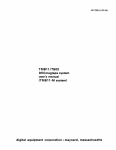
1
DV11 communications
multiplexer
user's manual
EK-OV11-0P-001
DV11 communications
multiplexer
user's manual
digital equipment corporation • maynard, massachusetts
1st Edition, December 1976
Copyright © 1976 by Digital Equipment Corporation
The material in this manual is for informational
purposes and is subject to change without notice.
Digital Equipment Corporation assumes no responsibility for any errors which may appear in this
manual.
Printed in U.s.A.
This document was set on DIGITAL's DECset-8000
computerized typesetting system.
The following are trademarks of Digital Equipment
Corporation, Maynard, Massachusetts:
DEC
DECCOMM
DECsystem-l0
DECSYSTEM-20
DECtape
DECUS
DIGITAL
MASSBUS
PDP
RSTS
lYPESET-8
lYPESET-ll
UNIBUS
CONTENTS
Page
CHAPTER 1
INTRODUCTION AND GENERAL DESCRIPTION
1.1
1.2.1
1.2.1.i
1.2.1.2
1.2.2
1.3
1.3.1
PURPOSE AND SCOPE . . . . . . . . . . . .
DVII COMMUNICATIONS MULTIPLEXER .
DVll Overview Block Diagram
Establishing the Data Link
DVll Operation . .
Reference Documents
PHYSICAL DESCRIPTION
General Specifications
CHAPTER 2
INSTALLAnON
2.1
2.1.1
2.1.2
2.1.3
2.1.4
2.1.4.1
2.1.4.2
2.1.4.3
2.1.5
2.3.1
2.4
2.4.1
2.4.2
2.4.3
2.4.4
2.5
SITE PREPARATION AND PLANNING
Minimum Through Maximum Configurations .
Compatibility Considerations and Precautions
Interface Specifications and Signals . . . . .
Interrupt Priorities and Address Assignments
Interrupt Priorities
........ .
Interrupt Vector Address Assignment
Address Assignments
Environment . . . . . . . . . . . . .
UNPACKING AND INSPECTION . . . . .
INSTALLATION OF BASIC ASSEMBLIES
Unibus Cable Interconnections . . . .
MODULE INSTALLATION AND CUSTOMIZING
Unibus and Interrupt Vector Address Assignments
Synchronous Parameter Selection
Resistance Checks . . . . .
Installation of Add-On DVll
SYSTEM CHECKOUT . . . . . .
CHAFfER 3
PROGRAMMING
3.1
3.1.1
3.1.2
3.1.2.1
3.1.2.2
3.1.2.3
3.1.2.4
3.1.3
3.1.3.1
3.1.3.2
3.1.3.3
3.1.3.4
3.1.3.5
3.1.4
3.1.4.1
3.1.4.2
PROGRAMMABLE FACILITIES AND FUNCTIONS
Programmable Registers
Control Table . . . . . . .
Control Table Format
Receive Control Byte
Transmit Control Byte
Control Byte Symmetry
Operations With Directly-Addressable Registers
Modem Setup and Control
Accessing Secondary Registers
Data Transfer Enabling
Interrupt Enabling and Response
Extended Memory Addressing
Protocol Processing . . . . . . . .
BCC Polynomial Selections
Processing Block Terminations
1.2
2.2
2.3
iii
1-1
1~1
1-1
1-2
1-2
1-3
1-3
1-3
2-1
2-1
2-1
2-2
2-2
2-2
2-2
2-2
.... ....
~-~
·
·
..
·
2-4
2-4
2-5
2-5
2-5
2-13
2-16
2-16
2-17
3-1
3-1
3-4
3-4
3-4
3-5
3-5
3-5
3-5
3-6
3-6
3-6
3-6
3-6
3-6
3-6
CONTENTS (Cont)
Page
3.1.4.3
3.1.4.4
3.1.4.5
3.1.4.6
3.1.4.7
3.1.5
3.1.5.1
3.1.5.2
3.2
3.2.1
3.2.2
3.2.3
3.2.4
3.2.5
3.2.6
3.2.7
3.2.8
3.2.9
3.3
3.3.1
3.3.2
3.3.3
3.3.4
3.3.5
3.3.6
3.3.7
3.3.8
3.3.9
3.3.10
3.3.11
3.3.12
3.3.13
3.3.14
3.3.15
3.3.16
3.4
3.5
3.5.1
3.5.2
3.6
3.6.1
3.6.2
3.6.3
3.6.4
3.6.4.1
3.6.4.2
3.6.5
3.6.5.1
3.6.5.2
Control Byte Inhibit . . .
. . . . . . . . . . . . . . . . . . .
Sync Character Selection
. . . . . . . . . . . . . . . . . . .
Sync/Mark State Select
. . . . .. . . . . . . . . . . . .
Stripping Received Syncs . . . . . . . . . . . . . . . . . . . . . .
Line Activity Snapshot
. . . . . . . . . . . . . . . . . . . . . . . .
Data Transfer Operations . . . . . . . . . . . . . . . . . . . .
Provision for Alternate Data Transmission Tables . . . . . . . . . . . .
Table Size and Location . . . . . . . . . . . . . . . . . . . . . . . . .
DIRECTLY-ADDRESSABLE REGISTERS . . . . . . . . . . . . . . . . . .
System Control Register (SCR) . . . . . . . . .
. . . . .
Line Control Register (LCR) . . . . . . . . . .
....
Receiver Interrupt Character Register (RIC)
NPR Status Register (NSR) .. . . . . . . . . .
. . . . . .
.
Reserved Register . . . . . . . . . . . . . . . .
. . . . . .
.
Special Functions Register (SFR) . . . . . . . .
. . . . . .
.
Secondary Register Selection Register (SRS) . . . .
. . . . . .
.
Secondary Register Access Register (SAR) . . . . .
. . . . . .
.
Modem Control Registers . . . . . . . . . . . . . . . . . . . . . . . . . . . .
.
INDIRECTLY ADDRESSABLE (SECONDARy) REGISTERS . . . . . . . . . . . . . . .
. . . . . . . . . . .
Transmitter Principal Current Address (0000)
. . . . . . . . . . .
Transmitter Principal Byte Count (000 I) .. . . .
. ..........
Transmitter Alternate Current Address (0010) ..
. . . . . . .
Transmitter Alternate Byte Count (00 II)
. ........
Receiver Current Address (0100) . . . . . . . . .
Receiver Byte Count (0101) . . . . . . . . . . . .
. ..........
...............
Transmitter Accumulated Block Check Character (0110)
Receiver Accumulated Block Check Character (0111)
.... ,
....
. . . . .
... .
Transmitter Control Table Base Address (I (00)
Receiver Control Table Base Address (100 1) .
. . . . .
.. . .
Line Protocol Parameters (1010) . . . . . . .
. . . . .
. ..
. . . . . . . . . . . .
. ..
Line State (lOll) . . . . . . . . . . . . . . .
Transmitter Mode Bits (1100)
. . . . . . . . .
. ..
Receiver Mode Bits (1101) . . . .
. . . . . . . . .
. ..
. ..............
Line Progress (1110) . . . . . . . . . .
Receiver Control Byte Holding (1111) .
. . . . . . . . .
. . .
CONTROL BYTE FORMAT.
. . . . . . . . . . . .
. . . . . . . . . . . . . .
DVl1 INITIALIZATION
. . . . . . . . . . . .
. ..............
Line Modem Set-Up
. . . . . . . . . . . . . . . . . . . . . . . . . .
DVl1 Data Transfer Setup.
. . . . . . . . . . . . . . . . ..
. .....
DATA TRANSFER IMPLEMENTATION
.......................
Originating and Answering Calls
. . . . . . . . . . . . . . . . . . . . . . . . . .
.
Resynchronization During Reception . . . . . . . . .. . . . . . . . . . . .
. .
Termination of Transmission and Reception . . . . . . . . . . .
BISYNC Implementation . . .
. . . . . . . . . . . .
. .
Transmission Control . . . . . . . . . . . . . . . . . . . .
. .
Reception Control . . . . . . . . . . . . . . . . . . . . . .
. .
DDCMP Implementation . . . . . .
. . . . . . . . . . . . . . . . . . . . . .
Transmission Control
. . . . . . . . . . . . .
. .....
Reception Control . . . . . . .
. . . . . . . . . . . . . . . . . . . . . .
iv
3-7
3-7
3-7
3-7
3-7
3-7
3-7
3-8
3-8
3-8
3-8
3-15
3-15
3-20
3-20
3-20
3-24
3-24
3-29
3-29
3-29
3-32
3-32
3-32
3-32
3-32
3-32
3-33
3-33
3-33
3-33
3-33
3-33
3-33
3-33
3-39
3-41
3-41
3-41
3-41
3-42
3-42
3-42
3-43
3-43
3-43
3-47
3-47
3-48
CONTENTS (Cont)
Page
APPENDIX A
PDP-II MEMORY ORGANIZATION AND ADDRESSING CONVENTIONS
APPENDIX B
PROTOCOLS FOR BINARY SYNCHRONOUS COMMUNICATIONS
APPENDIX C
GLOSSARY OF TERMS AND ABBREvlAnONS
ILLUSTRATIONS
Figure No.
1-1
1-2
2-1
2-2
2-3
2-4
2-5
2-6
2-7
3-1
3-2
3-3
3-4
3-5
3-6
3-7
3-8
Page
Title
DVll Overview Block Diagram
DV 11 Communications Multiplexer
DVll Interconnection Diagram
Module Utilization Diagram
DVll M7836 Module - Device Address Selection Switches
DVll M7837 Module - Interrupt Vector Address Selection
Switches for DVll Data Handling Section . . . . . . . . .
DVll M7807 Module - Device Address Selection Jumpers
and Interrupt Vector Address Selection Jumpers for DVll
Modem Control Unit .. . . . . . . . . . . . . . . . . . .
Location of Sync Switches on M7839 Module . . . . . . .
Distribution Panel and Test Connector Jumper Configuration
Control Byte Address
Control Byte Formats
DV 11 Primary Registers
DVl1 Secondary Registers
BISYNC Transmission Flow Diagram
BISYNC Reception Flow Diagram .
DDCMP Transmission Flow Diagram
DDCMP Reception Flow Diagram
1-2
1-5
2-4
2-6
2-7
2-8
·
2-9
· 2-14
· 2-18
3-4
· 3-5
· 3-9
· 3-30
. . . 344
· 3-46
.. 3-48
.. 3-49
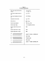
TABLES
Table No.
1-1
2-1
2-2
2-3
2-4
2-5
3-1
3-2
3-3
Title
Reference Documents
EIA Electrical Specifications
Device Address Switches ..
Vector Address Switches for Data Handling Section
Vector Address Jumpers for Modem Control Unit
Synchronous Parameter Selection Switches
Functions of DVII Programmable Registers
System Control Register Bit Assignments
Line Control Register Bit ASSignments
(For Synchronous Line Cards) . . . . .
v
Page
1-4
2-3
· 2-10
· 2-11
· 2-12
· 2-15
3-2
3-12
· 3-14
TABLIS (Cont)
Table No.
34
3-5
3-6
3-7
3-8
3-9
3-10
3-11
3-12
3-13
3-14
3-15
TItle
Line Control Register Bit ASSignments
(For Asynchronous Line Cards)
Receive Function Interrupt Conditions
(For Synchronous Line Cards) . . . .
Receive Function Interrupt Conditions
(For Asynchronous Line Cards)
Transmit Function Interrupt Conditions . . . . .
Control Status Register Bit Assignments
Line Status Register Bit Assignments
line Protocol Parameters Secondary Register Bit Assignments
Line State Secondary Register Bit ASSignments
Line Progress Secondary Register Bit Assignments
Control Byte Bit Assignments . . . . . . .
Transparent Data Transmission Control
Non-Transparent Data Transmission Control
vi
Page
· 3-16
· 3-21
·
·
·
·
·
·
3-22
3-24
3-25
3-28
3-34
3-35
· 3-37
· 340
· 345
· 3-45
CHAPTER 1
INTRODUCTION AND GENERAL DESCRIPTION
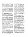
1.1 PURPOSE AND SCOPE
This manual is intended to provide operational programming information for the DVll Communications Multiplexer. The manual consists of three
chapters plus appendices:
8 or 16 serial data lines can be multiplexed directly to
PDP-II core memory for bidirectional data transfer.
The DVII is intended for use with a PDP-II-program
that provides the rules or protocol which govern the
data transfers and the generation and interpretation
of data link control and character codes.
Chapter I provides an introduction and overall
functional and physical descriptions of the
DVII;
Protocols require processing to (1) monitor transmitted and received characters in order to identify
and respond to control characters, (2) maintain a
record of control and data transmission a nd reception sequences, and (3) compute the error checking
~ode (block check calculation) on each character
transmitted or received. The DVII performs these
functions, thus relieving the processor of this overhead. A Core Memory Control Table, set up by the
PDP-II program, is used by the DVII to direct the
processing of received and transmitted characters.
The control table is comprised of control bytes,
which form a one-to-one correspondence with each
cha~acter transmitted or received.
Chapter 2 contains site preparation, interfacing,
and installation information;
Chapter 3 includes all information necessary for
operation of the DV II via the PD P-II
program;
Appendices contain reference data, communications introductory data, and an extensive
glossary of terms and abbreviations.
The reader unfamiliar with communication line protocols should read Appendix B before attempting
Chapters I and 3.
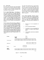
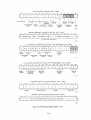
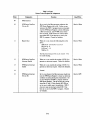
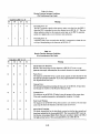
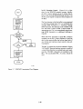
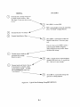
1.2.1 D VII Ol'eniew Block Diagram
Figure I-I is a DV II overview block diagram, showing the principal functional units, and data and control lines for the DV II. The DVII consists of two
primary functional subsystems, as indicated on the
block diagram: a Modem Control Unit, and a Data
Handling Section. The Modem Control Unit monitors and controls operations of the line modems as
directed by the PD P-II program. The Data Handling
Section sequences and synchronizes transfer of data
between the modems and the PDP-II Unibus (effectively, core memory).
Terms unique to the DVII are generally defined at
their first appearance. However, should the reader
encounter a word that is not fully understood, refer
to the glossary provided in Appendix C before
proceeding.
1.2 DVII
COMMUNICATIONS
MULTIPLEXER
The DV II is a communications multiplexer for the
PDP-II family of computers. By means of the DVII,
I-I
MODEM CONTROL
INTERRUPT
MODEM
CONTROL
UNIT
SET-UP
DATA LINES
TO
REMOTE
MODEMS
MODEMS
I
---------------~----DATA HANDLING
VI
::l
CD
Z
::l
Q.
oQ.
SYNC 6FLAGS
...------4
MICRO-
...------f
~------..
PROCESSOR
......----t 8
RECEIVED
CHARACTER
SILO
~-------"1
RECEIVER
INTERRUPT
CHARACTER
REGISTER
~--------~8~---------------------------------'
~--------~ 8
t--------------------------------------------11- Z896
Figure I-I
DVII Overview Block Diagram
1.2.1.1 Establishing the Data Link - Data transfer is
enabled whenever
Handling Section to enable the data transfer between
the selected local modem and core memory.
An operator manually initiates a call to a
remote modem, or the PDP-ll program
dials the remote number via the DNll
Automatic Calling Unit; when the data
link is established by the remote modem
answering the call, the DVII Modem
Control U nit signals the PDP-II program
via an interrupt.
The serial/parallel interface is accomplished in the
receivers and transmitters. The receivers assemble
characters received from the serial data lines and set a
flag each time a character is assembled. The transmitters disassemble parallel characters for transmission on the serial data lines and set a flag each time
another character can be accepted for transmission.
l.
2.
The M aster Scanner cyclically enables the receivers
and transmitters to route their flags to the
Microprocessor.
In response to a RING signal from a
remote modem, the DVII Modem Control Unit interrupts the PDP-II program,
to initiate an exchange of signals that
establishes the data link.
The Microprocessor is controlled by a Read-Only
Memory (ROM), which handles character transfers
and steps the Master Scanner. Once started by the
PDP-II program, the Microprocessor runs
continuously.
1.2.1.2 DVII Operation - With the data link established, the PDP-II program sets up the DVII Data
1-2
The Received Character (RC) Silo is a first-in, firstout storage buffer with a capacity of 128 characters.
When a character is received by the DVII and the
RC Silo is empty (usual condition), the character
propagates to the bottom of the RC Silo. The Microprocessor then inspects the character code to compute the core memory address of the control byte for
that character. A Non-Processor Request (NPR)
instruction is issued by the l\tficroprocessor to fetch
the control byte, which is then interpreted.
1.2.2 Reference Documents
Table 1-1 contains a list of pertinent documents, i.e.,
documents covering concepts and systems peculiar to
the DV II, plus documents covering equipment with
which the DVII interfaces.
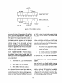
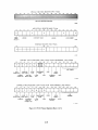
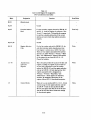
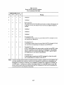
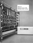
1.3 PHYSICAL DESCRIPTION
The DVII Communications MUltiplexer is housed in
a 9-slot, double system unit and includeS a separate
rack-mounted distribution panel for each group of
eight modems in a system. Figure 1-2 shows a DVII
system for supporting eight lines or modems. Other
configurations are discussed in Chapter 2.
In most cases, the control byte will specify character
storage, and the character will be transferred from
the bottom of the RC Silo to core memory via an
NPR transfer. Should the control byte identify the
character as an interrupt character, the character will
be propagated into the Receiver Interrupt Character
(RIC) register for further attention, and the PDP-ll
program will be signalled via an interrupt. The RICregister is used to display interrupt characters to the
PDP-II program, along with the line number and
any error flags.
1.3.1
General Specifications
Enfironment
Temperature: 10° to 50° C
Humidity: 0 to 90% non-condensing
Power Requirements
A DVII system with 16 synchronous lines:
Processing instructions for the character in the RIC
register are sent to the Microprocessor by the PDP-II
program The RC Silo continues to accumulate
received characters while waiting for the PO P-II program to complete its response to the interrupt; however, inspection and storage of any additional
characters from the RC Silo to PDP-II core memory
by the Microprocessor is inhibited. (The Microprocessor continues to perform data transmission
tasks.)
t7.5A@+5V
1.0 A @ -15 V
O.5A@+15V
A DVII system with 16 asynchronous lines:
20.5 A @ +5 V
1.0A@-15V
0.6 A @ +15 V
A DVII with 8 synchronous and 8 asynchronous lines:
NPR Control is used by the Microprocessor to access
core memory, to store received characters, fetch characters for transmission, and fetch control bytes to
direct character processing. Table addresses in core
memory are stored in the Random Access Memory
(RAM) for character storage and retrieval, and byte
counts for controlling the quantity of data transferred. The RAM also contains registers for controlling protocol functions for each data line.
19.0 A @ +5 V
1.0 A @ -15 V
0.55 A @ +15 V
Character Length
5, 6, 7, or 8 bits
Internal Baud Rates Profided
Synchronous (via switch settings):
1200, 2400, 4800, 9600
Character transmission is similar to the reception
process just described. When the Master Scanner
finds a transmitter flag, the Microprocessor uses
N PR Control to fetch the next character for that line
from core memory, it then uses the character code to
compute the address of the corresponding control
byte, and does an NPR to fetch the control byte. The
Microprocessor responds as directed by the control
byte and then loads the character into the transmitter
for transmission.
Asynchronous (via PDP-II program):
50,75, 110, 134.5, 150,300,600, 1200,
1800, 2000, 2400, 3600, 4800, 7200, 9600,
38,400
Operating Modes
Full- or Half-Duplex
1-3
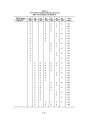
Table 1-1
Reference Documents
Title
Description
GENERAL
PDP-II Peripherals Handbook
Discussion of overall system, addressing modes, and basic instruction set from a programming point of view. Some interface and
installation data.
PDP-II Instruction List
Pocket-size list of instructions. List group names, functions, codes,
and bit assignments. Includes ASCII codes and the bootstrap
loader.
Logic Handbook
Presents functions and speCifications of the M-Series logic modules
and accessories used in PDP-II interfacing. Includes other types of
logic produced by DEC but not used with the PDP-II.
Introduction to Minicomputer Networks
Principles of computer-based data communications technology.
Binary Synchronous Communications
Introduction to IBM's Binary Synchronous Communications
Protocol (BISYNC or BSC).
A Message-Oriented Protocol for
Interprocessor Communication
Introduction to DEC's Digital Data Communication Message
Protocol (DDCMP).
Data Set 20lA and 20lB Interface
Specifications
Description of interface leads in synchronous modems.
Data Set 201 C Interface Specification
Interface Specification
Data Set 208A Interface Specification
Interface Specification
Data Set 208B Interface Specification
Interface Specification
SOF1WARE
Paper-Tape Software Programming
Handbook
Detailed discussion of the PDP-II software system used to load,
dump, edit, assemble, and debug PDP-II programs. Also included
is a discussion of input/output programming and the floating-point
and math package.
1-4
Figure 1-2
DVII Communications Multiplexer
Parity Generation and Detection
Odd, Even, or None
Sync Character Facility
Synchronization of a line can be selected to be
on the basis of the receipt of either one sync
character or two consecutive, identical sync
characters. For each 4-line group, two sync
codes may be manually preset in switches. The
PD P-II program may select either of those two
sync codes for use on a selected line.
Modems Accommodated
Synchronous modems (Bell System 201, 208,
209, or equivalent)
Asynchronous modems (Bell System 202 series,
103 series or equivalent)
Bus Loading
Two PDP-II Unibus Loads
NOTE
Since the DVll requires 21 A of +5 V power, only
three DVl1s can"e placed on a typicaI21-in. expander
box. Expander boxes usually contain three H744 regulators, each of which has a capacity of 25 A. A device
cannot be powered partially from one regulator and
partially from another regulator; the number of DVl1s
must equal the number of regulators. Therefore, three
DVlls is the maximum for one expander box.
Protocols Implemented
The DV II specifically implements (but is not
limited to) Digital's DDCMP and IBM's BISYN C protocols.
Maximum Throughput
38,400 characters/second
1-5
CHAPTER 2
INSTALLATION
This chapter provides information for interfacing,
installing, and testing the DVII Communications
Multiplexer. Interfacing considerations are discussed
in Section 2.1, Site Preparation and Planning. Installation, customizing, and checkout procedures are discussed in Sections 2.2 through 2.7.
2.1
2.1.2 Compatibility Considerations and Precautions
The DVII with synchronous line cards is directly
compatible with Bell synchronous modems 201, 208,
209, or equivalent. It is also compatible with Bell
asynchronous modems 202 series, 103 series or equivalent when asynchronous line cards are used. The
DVII provides internaal clock rates of 1200, 2400,
4800, and 9600 baud at 0.005% accuracy for synchronous operation; modems operating at other rates
must supply their own clock signals. It is recommended that modem-supplied clocking be used where
available.
SITE PREPARATION AND PLANNING
2.1.1 Minimum Through Maximum Configurations
The DVII provides multiplexing capability to PDPi I core memory for up to 16 modems. The DVII is
housed in a nine-slot, double system unit and includes one rack-mounted distribution panel for each
group of eight modems in a system. Five of the nine
slots are occupied by functions required in any system configuration. The remaining four slots are occupied by four hex-printed circuit boards (M7839 or
M7833), designated as the line cards. Each line card is
capable of supporting data transfers to and from four
modems. The M7839 line card supports synchronous
data transfers while the M7833 supports asynchronous data transfers (these line cards contain the
receivers and transmitters).
The DVII is compatible with all members of the
PD P-II family of computers. PDP-II standard software address allocations provide for the implementation of as many as four DVlls in a PDP-II system.
DVII throughput rate, however, forms a more severe
limitation on the number of DVlls in a system, as
will now be demonstrated.
A single DVII mUltiplexing 16 modems at 9600
baud, each in full duplex mode, is capable of transferring 38,400 8-bit characters per second (1200 characters per line X 16 lines X 2 directions). Although this
is well within the capabilities of the DVll, on the
average, the PDP-ll is provided with only 26 IlS to
handle each character. Although most characters are
handled by NPR transfers, program and protocol
efficiencies still need to be relatively high to maintain
this rate; this would be for a single DVII. Some
76,800 NPR cis would be required, or about 10 percent of Unibus capacity. With all lines operated in
DDCMP mode (control byte fetch inhibited), 38,400
NPR cis would be required, or about 5 percent of
Unibus capacity.
The 5-module unit common to all DV 11 configurations is designated the DVII-AA. Two of the
M7839 module, plus one distribution panel and associated cables, form an eight line synchronous unit
designated the DVII-BA. An eight line asynchronous
unit, the DVll-BB, is generated by replacing the
M7839 modules in the DVII-BA unit with two
M7833 modules. Similarly, a mixture of one of each
line card forms a synchronous/asynchronous unit
designated the DVII-BC. The minimum DVll system configuration consists of one DVII-AA unit plus
one line card option, DVII-BA, DVII-BB or DVllBC; a maximum configuration consists of one DVllAA unit plus two line card options.
2-1
DVlls should be connected ahead of all Massbus
devices on the Unibus and behind unbuffered NPR
devices such as RK05s. DVlls have placement
requirements similar to those for DQIls. If both
DQ II sand DV II s are used, place the units with the
highest baud rate first. If all DVlls have 16 lines at a
9600 baud rate, a maximum of I DVII can be connected with the following exceptions:
2.
The devices are assigned in order by type:
DCII; KLII/DLII-A, -B; DPll; DMIIA; DN II; DMII-BB; DRII-A; DRll-C;
PA611 Reader; PA611 Punch; DTll;
DXII; DLll-C, -D, -E; DJII; DHll;
GT40; LPSII; VT20; DQII; KWII-W;
DUll; DUPII; DVII Data Handling
Section/DVII Modem Conrol Unit.
a.
Two DVlls can be used on a PDP-l 1/40,
PDP-I 1/45, or PDP-II/50 with no disks.
3.
If any type device is not used in a system,
vector assignments move down to fill the
vacancies.
b.
Two DVlls can be used on a PDP-II/70
with no Unibus disks.
4.
I f additional devices are to be added to the
system, they must be assigned contiguously after the original devices of the
same type. Reassignment of other type
devices already in the system may be
required. (For example, the vector for
another DVII would be after the existing
DV II, but addition of a DC II would
cause all other vector addresses to move
upward.)
For lower speed lines, the maximum number can be
increased proportionally. (Example: a PDP-II/40
with 2400 baud rate lines can use four DVlls.) A
maximum of four DV lis can be placed on any system because of address space limitations; the limitations are based on NPR access. Interrupt
performance depends on the operating system, protocol, and buffer lengths.
Each device interrupt vector requires four address
locations (two words). A further constraint is that all
vector addresses must end in 0 or 4. The vector
address is specified as a three-digit, binary-coded
octal number using Unibus data bits 0-8. Because the
vector must end in 0 or 4, bits I and 0 are not specified (they are always 0) and bit 2 determines the least
significant octal digit 0 f the vector address (0 or 4).
2.1.3 Interface Specifications and Signals
The DVII presents two unit loads to the PDP-II
Unibus and also provides modem control and data
leads compatible with EIA RS-232-C and CCITTV24 specifications. EIA RS-232-C electrical specifications are listed in Table 2-1.
2.1.4
Interrupt Priorities and Address Assignments
2.1.4.3 Address Assignments - The DVII is assigned
an address of 77S000. Additional DVlls would be at
77S04O, 77S100, 77S140, etc. If any DMII-AAsarein
use, the DVII will follow them.
2.1.4.1 Interrupt Priorities - The DVII uses three
interrupt vector addresses. Interrupt priorities for the
Data Handling Section are selectable by means of a
priority plug on the M7837 module. The priority plug
is preset to select BRS priority; it may be changed to
select BR6 priority, but the diagnostic programs
expect BR5. The Modem Control Unit is permanently wired to BR4 priority.
2.1.5 Environment
The DVII will operate in temperature environment
from 10° to 50° C with a relative h~midity up to 90%,
non-condensing. Power requirements are as follows:
2.1.4.2 Interrupt Vector Address Assignment - Communications devices are assigned floating interrupt
vector addresses as follows:
I.
Voltage
+S
-IS
+IS
The vector space starts at location 300 and
proceeds upward to 776.
2-2
Current
(Amperes)
21
1
O.S
Table 2-1
EIA Electrical Specifications
Driver output logic levels with 3K to
7K load
is V>oh> S V
-5 V >01> -15 V
Driver output voltage with open circuit
IV 0 1< 25 V
Driver output impedance with power
off
20>300 ohms
Output short circuit current
dv
Driver slew rate
dt < 30 Vps
Receiver input impedance
7KO> R in > 3KO
Receiver input vol tage
± 15 V compatible with driver
Receiver output with open circuit
input
Mark
Receiver output with +3 V input
Space
Receiver output with -3 V input
Mark
+15
+5
IZ/fl//T/I
LOGIC "0"= SPACE - CONTROL ON
Noise margin
+3
0
-3
S\\\\\\\\\
Transition region
~\~\\~~\\
Noise margin
-5
-15
/7////////
LOGIC "1" = MARK = CONTROL OFF
2-3
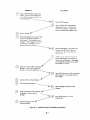
~.2 UNPACKING AND INSPECfION
\fter unpacking, check that the following parts are
)resent for the basic DVII-AA unit:
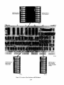
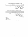
2.3 INSTALLATION OF BASIC ASSEMBLIES
Drawing D- UA- DV 11-0-0 shows the physical
arrangement of the wired backplane, distribution
panel(s) and cables in a typical installation. Figure 2I is the DV 11 interconnection schematic. Install the
9-slot, double system unit in the expander box or
processor box as space and power are available. With
power off, test the resistances between all pins of the
power harness Mate-N-Lok connector. Only pins of
the same wire color should be connected. Secure the
ground wire to one of the mounting screws. Plug in
the Mate-N-Lok connector of the power harness.
Apply power and check for proper voltages on the
logic pins (not the cable) as follows:
I D-AD-7010834-0-0 Logic Assembly
I M7807 Bus Control and Mux Board
I M7808 Modem Control Scan and M ux Board
I M7836 ALU and Transfer Bus Board
I M7837 Unibus Data and NPR Control Board
I M7838 ROM, RAM, and Branch Board
I M920 Unibus Connector
\Iso check that the following parts are present for
:ach line card option ordered:
Pin
CIA2
CIB2
CIUI
Voltage
+5 ± 0.25 V
-15 ± 0.75 V
+15 ± 0.75 V
2 H8612 Line Card Test Connectors
1 H 317C Distribution Panel
4 BC08R-15 Cables
I H325 Test Connector
This will ensure that the cable and the Mate-N-Lok
connector were correctly installed. Turn power off.
(Note that the DVII is not yet connected to the
Unibus, nor are any modules installed.)
DVII-BA: 2 M7839 Sync Mux Line Card
DVII-BB: 2 M7833 Async Mux Line Card
Install the distribution panel(s) as indicated in Figure
2-1. Refer to Figure 2-7 for the proper jumper configuration of the distribution panel. To install an addon DVIl, see Paragraph 2.4.4.
DVII-BC: I M7839 Sync Mux Line Card;
M7833 Async Mux Line Card
OUTPUT CABLES
ARE BC...o5D-25
8 OUTPUT CABLES
LINE CARD SLOT 5
H317C
DISTRIBUTION PANEL
(FIRST 8 LINES)
M
LIN
JI
LOT
4 BCOIR
CABLES
PO Pll PROCESSOR BOX
OR BAIt EXPANDER
BOX THAT CONTROL
THE DVII CONTROL
LOGIC WIRED ASSY
D-AD-7010834
4 BCOIR
CABLES
H317C
DISTRIBUTION PANEL
(SECOND I LINES)
AC POWER CORD
TO LINE OR PDP-l1
NOTE:
Install all BC08R cables with smooth
side toward you and ribbed side toward
circuit board.
11- 2.50
Figure 2-1
DVII Interconnection Diagram
2-4
DVII. Two Unibus addresses (also called device
addresses) and two interrupt vector addresses are
provided on the D V II as follows:
2.3.1 Unibus Cable Interconnections
The DV II is shipped with one M920 Unibus Connector (placed in slot 9 as shown in the module utilization program, Figure 2-2), which provides for
electrically connecting the unit to the PDP-II
Unibus. For processor box installation where the unit
is to be electrically placed in mid-bus (i.e., somewhere
between the first and last devices on the PDP-II
Unibus), the M920 from the next higher device
(closer to the processor) on the bus is plugged into
slot I of the DVII, and the M920 in slot 9 of the
DVII is plugged into slot I of the next lower device
on the bus.
Remove the M930 Unibus Terminator
from the last slot of the current end-of-bus
device.
2.
Remove the M920 from slot 9 of the
DVII and place in slot I of the DVII.
3.
Install the M930 (removed in step I) in
slot 9 of the DVll.
DVII Data Handling Section address,
2.
DVII
3.
DV i i Data Handiing Section interrupt
vector address,
4.
DVII MCU interrupt vector address.
~fCU
address,
Because the DV II has ten registers directly addressable by the PDP-II program, it must be assigned a
Unibus address that is a mUltiple of 32 (octal 40). All
DV II s in a system should have consecutive
addresses.
For an end-of-bus installation of the DVII, proceed
as follows:
I.
1.
The Unibus addresses for the DVII Data Section are
controlled by a rocker DIP switch package, located
on module M7836, and by jumper straps on module
M7807 for the DVII MCU. (Locations of all address
selection switches and jumpers are shown in Figures
2-3 through 2-5.) The position of these switches determines bits 03-12 of the Unibus address. If a rocker
switch is set to ON or a jumper on the M7807 board
is in, an address bit of zero in the corresponding bit
position serves to address the DVII Data Handling
Section. DEC standard software requires that the
DVII address be set as specified in Paragraph 2.1.4.
Switch settings for device address selection are shown
in Table 2-2.
Unibus interconnections are made via BCII-A cables
where the DV II is installed in expander box or is
physically the first or last unit in any box. Cable
requirements in these cases are as described in Figure
2-2.
2.4 MODULE INSTALLATION AND
CUSTOMIZING
Figure 2-2 is the module utilization diagram. Set the
address assignment and parameter selection switches
as described in Paragraphs 2.4.1 and 2.4.2 before
installing modules.
The interrupt vector address for the Data Handling
Section is controlled by a DIP switch package on the
M7837 module, which selects vector address bits
08-03. The switches should be set to select vector
addresses between 300 and 776. Switch settings for
interrupt vector address selection for the Data Handling Section are shown in Table 2-3. Vector address
selection for the Modem Control Unit is done by
jumpers on the M7807 module (Table 2-4).
2.4.1 Unibus and Interrupt Vector Address
Assignments
The Unibus and interrupt vector addresses for the
DV II must be set manually before operating the
2-5
1
2
3
4
5
6
7
8
M920
M7836
M7837
M7838
M78391
~+~~r
~i~~~1
~~~~~I
M7833
CABLE
A
UNIBUS
CONNECTOR
NOTE 3
9
M920
CABLE
ALU
AND
TRANSFER
BUS
UNIBUS
DATA
AND
NPR
CONTROL
ROM
RAM
AND
BRANCH
MUX
LINE
CARD
MUX
LINE
CARD
MUX
LINE
CARD
MUX
LI NE
CARD
UNIBUS
CONNECTOR
NOTE 1
LINES
0-3
LINES
4-7
LINES
8-11
LINES
12-15
NOTE 2
S
B
C
M7807
M7808
BUS
CONTROL
AND
MUX
MODEM
CONTROL
SCAN
AND
MUX
-
0
E
-
F
VIEW FROM WIRING SIDE
NOTES:
t. If end of bus replac. M920 with M930.
2.If last unit in basic box replac. M920 with BCllA cable
end wh.n .xpanding to ph'riphtral box.
3-.If first unit in expander box r.place M920 with BCttA cable end.
'1- 2932
Figure 2-2
Module Utilization Diagram
2-6
A12
A11
A10
A09
AOS
ON=O
OFF = 1
A07
A06
A05
A04
UNUSED
7414-3
Figure 2-3 DVII M7836 Module - Device Address Selection Switches
2-7
7414-1
Figure 2-4 DVll M7837 Module - Interrupt Vector Address Selection Switches
for DVll Data Handling Section
2-8
DEVICE ADDRESS
(A03 -A12)
W18
W12
W17
Jumper
W8
W9
Wl0
Wll
W12
W13
W14
W15
W16
W16
W17
W13
Bit
A12
A09
AOS
Al0
A04
A06
A11
A03
A06
A07
Jumper In-O
Wl0
Wll
W9
W5
INTERRUPT VECTOR
ADDRESS
(002 -DOS)
W8
Jumper
Bit
DOS
002
003
006
007
005
004
Jumper In = 1
W1
W2
W3
W4
W5
W6
W7
W15
W1
W14
W2
W7
W3
W4
W6
7414-11
Figure 2-5 DVII M7807 Module - Device Address Selection Jumpers
and Interrupt Vector Address Selection Jumpers
for DVII Modem Control Unit
2-9
Table 2-2
Device Address Switches
M7807 Jumper
M7836 Switch
Address Bit
-o
IV
I
W8
I
AI2
WI4
2
All
X
X
X
X
X
X
X
X
X
X
X
X
X
X
X
X
X
X
X
X
X
X
X
X
X
X
X
X
X
X
Wll
3
AIO
W9
4
A09
WIO
S
AOS
WI6
6
A07
WI7
7
A06
WI3
8
AOS
WI2
9
A04
A03*
Device
Address
Notes
775000
First DV 11
X
775020
775040
First DV 11 MeV
Second DVII
X
775060
775100
Second DV II MeV
Third DVl1
X
775120
775140
Third DVII MeV
Fourth DVII
X
775160
Fourth DVII MeV
X
X
WIS
Note: X means switch off (M7836) or Jumper out (M7807).
*Bit 3 selection applies to M7807 only. No bit 3 switch is provided on M7836 module.
Table 2-3
Vector Address Switches for Data Handling Section
(Vector Addresses are Modulo 10)
M7837 Switch
Address Bit
1
5
4
D05
D04
6
D03
x
X
X
X
X
X
X
X
X
X
X
D08
2
D07
3
D06
Vector
Address
300
310
X
320
330
X
X
X
X
X
X
340
350
X
360
370
X
X
X
X
X
X
X
X
X
X
X
X
X
X
X
X
X
X
X
X
X
X
X
X
X
X
420
X
430
440
450
X
X
X
X
X
X
X
X
X
X
X
500
510
X
520
X
530
540
550
X
X
X
460
470
X
X
400
410
X
X
X
X
560
570
etc. to
770
Notes:
1.
X means switch ON
2.
Set only the switches shown.
3.
Vector Address Bit 002 is controlled by DVII logic dependent on
whether a Receiver Interrupt (Bit 002 = 0 = Vector A) or a
Transmitter Interrupt (Bit 002 = 1 = Vector B) is being requested.
2-11
Table 2-4
Vector Address Jumpers for Modem Control Unit
(MCU Vector Addresses are Modulo 4)
M7807 Jumper
Address Bit
WI·
DOS
WS
007
W4
006
W6
DOS
W7
004
W3
003
W2
D02
X
X
X
X
X
X
X
X
X
X
X
X
X
X
X
X
X
X
X
X
X
X
X
X
X
Vector
Address
300
304
X
310
314
X
320
324
X
330
334
X
X
X
X
X
X
X
X
X
X
X
340
344
X
350
354
X
X
X
X
X
X
360
364
X
X
370
374
X
X
X
X
X
X
X
X
X
X
X
X
X
X
X
X
X
X
X
X
X
X
X
X
X
X
X
X
X
X
X
X
X
X
X
400
404
X
410
414
X
420
424
X
430
434
X
X
X
X
X
X
X
X
X
X
X
X
X
X
X
X
X
X
X
X
X
X
X
440
444
X
450
454
X
460
464
X
470
474
X
X
X
X
X
X
X
X
2-12
X
500
504
Table 2-4 (Cont)
Vector Address Jumpers for Modem Control Unit
(MCU Vector Addresses are Modulo 4)
M7807 Jumper
Address Bit
WI·
D08
WS
D07
W4
D06
W3
D03
W6
DOS
W7
D04
X
X
X
x
X
X
X
X
X
X
X
X
X
X
X
X
W2
D02
X
Vector
Address
510
I
514
520
524
530
534
540
544
550
554
560
564
X
X
X
X
X
X
X
X
X
X
X
X
X
X
X
X
X
X
X
~70
X
X
574
X
etc. to
774
Notes:
1.
X means jumper OUT
2.
Cut only the jumpers shown.
3.
·Jumper WI is in for the PDP-I 1/20 with the K.HII and for the PDP-I 1/40,
PDP-I 1/45, and newer PDP-lIs.
1.4.1 Synchronous Parameter Selection
Rocker DIP switches are located on each M7839
module for selection of the following synchronous
data channel parameters:
J.
Internal baud rate (1200, 2400, 4800,
96(0)
2.
Full/half duplex
3.
Parity (odd/even/none)
4.
Character length (5, 6, 7, or 8 bits)
5.
Sync requirement (whether one sync character or two consecutive, identical sync
characters are required to achieve line
synchronization).
6.
Sync character codes
Switch settings for each synchronous parameter are
listed in Table 2-5. Switch locations are shown in Figure 2-6.
NOTE
Whenever possible, the parameters should be configured per customer requirements at this time. If halfduplex or parity operation is required, this configuration can only be done after diagnostics have been
run. DVll diagnostics don't support half-duplex or
parity operation.
2-13
SWITCH PACK 4
Sync Character A
SWITCH PACK 3
Sync Character B
7414-6
SWITCH PACK 2
Baud rate and
Duplex Select
SWITCH PACK 1
Parity. Character
length. and number
of syncs
7414-5
7414-4
Figure 2-6 Location of Sync Switches on M7839 Module
2-14
Table 2-5
Synchronous Parameter Selection Switches
Switch
Function
Internal Baud
Parameter
1200 Baud
Rate
2400 Baud
4800 Baud
9600 Baud
Full/Half
Full Duplex *
Duplex
Half Duplex
Name
Pack
Number
Select B
S2
3
Select A
S2
4
ON
~olo"t
0
~J""",",,\.U
S2
"2
..J
f""'\11..1
Select A
S2
4
OFF
Select B
S2
3
OFF
Select A
S2
4
ON
Select B
S2
3
OFF
Select A
S2
4
OFF
HD3
S2
5
ON
HD2
S2
6
ON
HDI
S2
7
ON
HDO
S2
8
ON
HD3
S2
5
OFF
HD2
S2
()
OFF
HDI
S2
7
OFF
s...,...
0
v -r'
PI
SI
I
OFF
EPE
SI
2
OFF
PI
SI
1
ON
EPE
SI
2
ON
PI
SI
I
ON
EPE
SI
2
OFF
WLSI
SI
3
OFF
WLS2
SI
4
OFF
WLSI
SI
3
ON
WLS2
SI
4
OFF
WLSI
SI
3
OFF
WLS2
SI
4
ON
WLSI
SI
3
ON
WLS2
SI
4
ON
1 SYNC 00
SI
5
OFF
1 SYNC 01
SI
6
OFF
I SYNC 02
SI
7
OFF
I SYNC 03
SI
8
OFF
1
Parity
No Parity*
Odd Parity
Even Parity
Character
8 Bits/Char
Length
(Excluding
7 Bits/Char
Parity)
6 Bits/Char
5 Bits/Char
SYNC
1 SYNC REQ.
Requirement
U
*Must be selected to run diagnostics DZDV A to DZDVE.
2-15
Setting
ON
V1'
Table 2-5 (Cont)
Synchronous Parameter Selection Switches
Parameter
Function
Sync Req. (cont)
Sync Character
2 SYNC REO.
Desired Code
Switch
Pack
Name
Number
1 SYNC 00
SI
5
ON
1 SYNC 01
SI
6
ON
1 SYNC 02
SI
7
ON
1 SYNC 03
Sl
8
ON
Sync A
S4
1
(As required
,j,
OFF=Logi-
Codes
Desired Code
S3
Sync B
8
cal one)
1
(As required
,j,
OFF=Logi-
8
cal one)
2.4.4
Installation of Add-On DVll
Proceed as follows to install an add-on DVll:
Line synchronization can be selected by the receipt of
either one sync character or two consecutive, identical sync characters. F or each 4-line group, two sync
codes (Sync A or Sync 8) may be manually preset in
the Sync Character Code switches. The PDP-ll program may select either of these two sync codes for use
on a selected line.
Internal baud rate is determined by the ON/OFF
states of the Select A and Select 8 switches. This is
applicable only when the modem does not supply
clocking.
2.4.3
Setting
1.
Install the wired backplane assembly in
the mounting box.
2.
Measure the resistance between pins of
the power harness (see first paragraph of
Section 2.3).
3.
Plug in the Mate-N-Lok connector of the
power harness.
4.
Apply power and measure voltages at the
logic pins (Paragrah 2,3),
5.
Turn power off.
6.
Set all address, parameter switches (Paragraphs 2.4.1 and 2.4.2) and distribution
panel jumpers (Figure 2-7).
7.
Install modules (Figure 2-2).
8.
Unplug the power harness.
9.
Do resistance checks (Paragraph 2.4.3).
Resistance Checks
Measure the resistance between the following pins on
the backplane with the white plug of the 7010835
cable hanging free (not plugged in), and with all modules plugged in:
n or greater
n or greater
n or greater
+5 V to GND must be 0.5
-15 V to GND must be 50
+ 15 V to GND must be 10
If the resistance is less than the lower limit indicated,
check for a short. If the resistance exceeds five times
the low limit, it may indicate an open circuit. Make
each measurement twice, once for each polarity of the
meter. The lowest reading must not be less than the
low limit listed. If the above resistances are correct,
connect the white plug in accordance with D-UADVII-O-O.
10.
2-16
Apply power.
2.5 SYSTEM CHECKOUT
Turn on the power. Toggle in the Bootstrap and load
the Absolute Loader (if not already done). The
addresses and contents of the Bootstrap Loader are
listed below.
Address
l"'f~_~_ •.
IVI~IIIVI
Y
~:_~
~IL~
.,,,,,
- - - I ....
Contents
1\ 1 £
.,1\ 1
VIU IVI
determines the
first 3 digits:
---746
000 026
---Equals:
017for4K
---750
---752
012702
000 352
037 for 8K
---754
005211
057 for 12K
---756
105 711
077 for 16K
---760
100376
117 for 20K
---762
116 162
137 for 24K
---764
000 002
I "7 for 2XK
---766
---400
---770
005267
---772
177756
---774
000 765
---776
177560
(TTY Reader)
or
177550
(High speed
reader)
Place Absolute Loader (MAINDEC-II-LZPA-PO)
in the reader, load and start at address ---744. Place
the diagnostic tape in the reader, load and start att
address ---500. Load and run the DVII diagnostics
as specified in Chapter 5 to verify system operation.
I f half-duplex or parity operation is desired, configure the M7839s accordingly (Table 2-5).
2-17
D!STR !BUT!ON PANEL
EIA CONNECTOR
H325
TEST CONNECTOR
P. GND
EIA XMIT DATA 00
EIA RCV DATA 00
J1-2 - - -.....\
RTS 00
J 1- 3 ------'.
CTS 00
J1-4~
J 1-5
S GND
CARRIER 00
J1-8
(202 SEC TX gg)
NEW
- - 1 - - - - - - 0 - - 0 - - . - SYNC
W02A
00
·1
J 1 - 1 1 - - -...
J1-i2 - - - - - - '
J1-15~
W06S
J1-24
DCE SCT 00
J1-17
W07S
-1------0--<>-- DCE SCR 00
J1-20----..
J1-22---~
( NEW*
SYNC
( "A"
DTR 00
J1-6---~
RI 00
J 1 - 1 4 - - -.....
W04S
-t-------<)--o-- DTE SCTE 00
- - 1 - - - - - - 0 - - 0 - - RTS 00
W05F
* NORMALLY
REMOVED
NOTES:
1. Jumper configuration is typical for remaining lines.
For actual jumper locations, refer to drawing D-CS-5411153.
2. For asynchronous use, remove jumpers denoted by the letter "S".
For synchronous use, remove jumpers denoted by the letters "A" or
"r"
11-4404
Figure 2-7
Distribution Panel and Test Connector Jumper Configuration
2-18
CHAPTER 3
PROGRAMMING
This chapter contains all information required for
controlling operation of the DVII Communications
Multiplexer by means of the PDP-ll program.
(Chapter I should be read prior to this chapter.) The
reader should also be familiar with synchronous protocols as discussed in Appendix B. Chapter contents
are arranged as follows:
I.
determine and respond to requirements for auxiliary
protocol processing (i.e., block check calculations,
data block terminations, control character handling).
The PDP-II program directs DVII activities through
the programmable registers of the DVII, along with
a control table set up in core memory for reference by
the DVII.
Programmable Facilities and Functions:
The programmable registers, core memory table references, and functions of the
DVi i are discussed (Section 3.i).
2.
Complete, detailed descriptions of programmable registers and control bytes
(Sections 3.2, 3.3, 3.4).
3.
Procedures for DVII initialization (Section 3.5).
4.
Methods for controlling data transfers
and implementing protocols (Section 3.6).
3.1.1 Programmable Registers
The DV i i programmable registers consist of the
"primary" system registers. which are directly
addressable via the Unibus, plus "secondary" registers, which may be accessed by the PDP-II program
after first loading a primary register. (The primary
register selects the secondary register to be accessed.)
The directly-addressable registers provide for modem
setup and control, data transfer enabling, interrupt
enabling and reporting, extended memory addressing, and access to secondary registers. The secondary
registers provide for protocol processing and data
transfer control.
Section 3.1 describes DV II functions in sufficient
detail to enable the reader to omit a detailed study of
the comprehensive reference data in Sections 3.2, 3.3,
and 3.4, and to proceed directly to the procedural
data in Sections 3.5 and 3.6.
Ten directly-addressable registers are provided.
There are 16 secondary registers provided for each of
the 16 multiplexed data channels, for a total of 256
secondary registers. The secondary registers make up
a separate Random Access Memory (RAM) within
the DV II. Secondary registers store functions that
may vary from line to line, and that require the extensive storage capacity of the RAM.
3.1 PROGRAMMABLE FACILITIES AND
FUNCfIONS
The DVII is a core memory-to-synchronous/asynchronous data line multiplexer with special
features to facilitate processing of a wide variety of
communication protocols. Under the overall direction of the PDP-II program, the DVII sets up the
data line modems, stores and retrieves data from core
memory, monitors and reports error conditions, and
examines each transmitted or received character to
Functions of programmable registers are described in
Paragraphs 3.2 and 3.3, following a discussion of the
control table. Functions, functional categories, and
table references for programmable registers are listed
in Table 3-1, which is provided for reference during
study of Paragraphs 3.1.3 and 3.1.4.
3-1
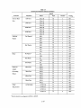
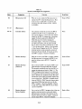
Table 3-1
Functions of DVll Programmable Registers
Type
Directly
Addressable
(Modem Control Unit)
Directly
Addressable
(Data Handling
Section)
Name
Control Status Register (CSR)
Initialization, Modem Enabling, Modem
Scanning, Interrupt Enabling, Interrupt
Requests.
line Status Register (LSR)
Modem Control, Modem Status
Reporting
Secondary Register Selection (SRS)
Secondary Register Selection, Line Selection
for line Control Register Bits 9-14.
Secondary Reg. Access Reg. (SAR)
Read or Write Selected Secondary Register
System Control Register (SCR)
Initialization, Interrupt Enabling & Requests,
Restart after Interrupt, Setting Extended
Address Bits.
Line Control Register (LCR)
Receiver Enabling, Sync Character Selection,
Extended Address Bits Read, Baud Rate Select.
Format Select.
Receiver Interrupt Character (RIC)
Receive Interrupt Code and Interrupt Character Storage.
NPR Status Register/Silo (NSR)
Transmit Interrupt Code Storage
Special Functions Register (SFR)
(Maintenance)
Reserved Register (RIR)
(Reserved)
Transmitter Principal Current
Address
Current Address for Transmitter Principal
Data Table
Transmitter Principal Byte Count
Byte Count for Principal Transmitter Data
Table
W
I
N
Indirectly
Addressable
(Secondary )
Functions
Functional Category
Modem Set Up and Control
Table
3-8
3-9
Secondary Register Accessing
-----
Data Transfer Enabling, Interrupt Enabling, Extended Memory Addressing
3-2
3-3,3-4
Interrupt Reporting
3-5,3-6
3-7
-------
-- ---
Data Transfer Control
- ----
Table 3-1 (Cont)
Functions of DVII Programmable Registers
Type
Indirectly
Addressable
(Secondary)
(Cont)
FUllctiOilS
Name
Transmitter Alternate Current
Address
Current Address for Tra nsmitter Alternate
Data Table
Transmitter Alternate Byte
Count
Byte Count for All ernat e Transmitter Data
Table
R(~ceiver
Current Address for Re(:eiver Data Table
Current Address
Re~eive:r
Receiver Byte Count
Byte Count for
Transmitter Accumulated BCC
Transmitter Accumulat(~d BCC
Receiver Accumulated BCC
Receiver Accumulated]3CC
Transmitter Control Table Base
Address
Transmitter Control Tal·lle Base Address
R(~ceiver
Receiver Controllable Base Address
Control Table Base
Functional Category
Table
Data Transfer Co ntrol
Data Table
Address
--.
line Protocol Parameters
Block Check Polynomi:: I Type, DLE Storage,
Stripping Received Syn :s, Idle Select
line State
Transmitter Enabling, Snapshot of line
activity. Action requin d on zero receiver
byte count (if marked).
Transmitter Mode Bits
Transmitter Mode now in use .
..
Receiver Mode Bits
Receiver Mode now in l Jse .
..
line Progress
Action Required on zer o transmitter byte
count (if Marked).
..
Receiver Control Byte Holding
Receiver Control Byte.s·'torage
..
Protocol Processi ng
3-10
3-11
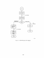
The mode field occupies bits 8, 9, and 10 and is
appended to the basic control table address to form
the actual address of the control byte. Thus, in the
example above, the control bytes for character code
101 would be in location 4101 (mode 0), location
450 I (mode 1), location 5101 (mode 2), etc. The control byte address formation sequence is graphically
depicted in Figure 3-1. Control byte formats are
shown in Figure 3-2.
3.1.2 Control Table
The control table contains the control bytes fetched
from core memory by the DV II each time a character
is received or is to be transmitted. The control bytes
are used by the DVII to control processing of the
transmitted or received character.
3.1.2.1 Control Table Format - The addresses in
core memory for each line of the receiver and transmitter control tables are set in secondary registers by
the PDP-II program. The DV II adds the character
code to the base address to form the basic core memory address of the control byte for that character. For
example, if the base address of the receiver control
table for a given line is 4000 and the character 101
code is received (ASCII letter A), 4101 would be
effective core memory address of the associated control byte.
3.1.2.2 Receive Control Byte - Whenever a character is input to the DV II from the data link receiver,
the associated control byte is obtained from core
memory by a Non-Processor Request (NPR) to specify the next mode and to dictate character disposition. The following character dispositions are
provided:
With this scheme, 256 locations (28) are sufficient to
provide control bytes for every possible 8-bit character code. In the usual protocol, however, certain
codes are susceptible to more than one mode of interpretation, depending upon the sequence in which
they are received and whether the data is transparent
or non-transparent. Thus, 3-bit mode specification
fields are provided in secondary registers for each line
in the transmitter and receiver functions. Sequencing
between modes may be effected by the control byte,
which specifies the mode in which the DVII is to
operate.
l.
Generate (or do not generate) an
interrupt.
2.
Store (or discard) the character.
3.
Accumulate (or do not accumulate) the
character in the Block Check Character
(BCC).
4.
Expect the BCC (treat the next character
as a BCC).
Parameter
EXTENDED
ADDRESS
BITS
ADDRESS
,-----""---v
17
Table Base Address
16
[~=[ ~
15
14
13
12
11
0
0
0
0
11
I I I I
10
09
08
07
06
05
04
03
02
01
00
0
0
0
0
0
0
0
0
0
0
0
01 1 1 0 11 1 0 1 0
11
I I I I I I I I I I I I
Character Code
Mode No.
Resultant
Address of
Control Byte
Shifted)
[~I~
1 0 1 0
10 1
1 0 1 0 1 0
I
0
1 0 11
I
11-2683
Figure 3-1
Control Byte Address
3-4
1_---&.
. . _______
1
.L...-_"""'"--_--'--_--L.._---"_x
.........
07
TRANSMIT CONTROL BVTE
00
RECEIVE CONTROL BYTE
DISCARD/STORE
X=NOT USED
EXPECT
BCC
INCLUDE CHAR
IN BCC
INTERRUPT
PROGRAM
11-2682
Figure 3-2
Control Byte Formats
The interrupt disposition provides for signalling the
program in the event of error conditions, or data link
control characters requiring special handling. The
character that caused the interrupt is loaded into the
RIC register. The program responds by sending a
special control byte to the OVI l, which would then
override the previous dispositions set for received
characters. The discard disposition provides for
inhibiting storage of data link control and other
unwanted characters. The do-not-accumulate disposition provides for the exclusion of non-data; BCC
anticipation signals characters from the error-checking process. BCC anticipation signals the DVII to
initiate data block termination procedure.
transmission command causes the OVII to retrieve
the OLE character from secondary register storage
and "stuffs" the OLE in front of the character to be
transmitted.
.1.1.2.4 Control Byte Symmetry - The receive and
transmit control bytes are configured so that a single
control table will provide for both transmit and
receive functions for a given line if the following functional limitations are observed:
3.1.2.3 Transmit Control Byte - Whenever a character is input to the DVII from PDP-II core memory,
the associated control byte is obtained from core
memory by a NPR to specify the next mode and any
other processing instructions. The following instructions a re provided:
I.
The protocol must progress from mode to
mode in a symmetrical fashion for both
transmit and receive;
2.
the same characters must be included in
the BCC for both transmit and receive.
For protocols that do not meet these requirements,
separate control tables may be used.
3.1.3
I.
Accumulate (or do not accumulate) the
character in the BCC.
2.
Send the BCC after the character.
3.
Send the D LE before the character.
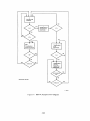
Operations With Directly-Addressable
Registers
The directly-addressable registers provide for modem
setup and control data transfer enabling, interrupt
enabling and reporting, extended-memory addressing
and access to secondary registers (see Table 3-1).
3.1.3.1
Modem Setup and Control - Modem
enabling. monitoring, and control are provided by
the Control Status Register (CSR) and the Line Status Register (LSR) of the Modem Control Unit. Stepby-step procedures for accomplishing these functions
are contained in Paragraphs 3.5 and 3.6.
As in the case of the receive control byte, the do-notaccumulate disposition provides for the exclusion of
non-data characters from the error-checking process.
The BCC transmission command signals the DVII to
initiate data block termination procedure. The DLE
3-5
3.1.3.2 Accessing Secondary Registers - The Secondary Register Selection Register (SRS) provides
for PDP-II program access to the secondary registers
in the DVII RAM. To address a secondary register,
the PO P-ll program sets the 8-bit RAM address,
consisting of the 4-bit line number, plus the 4-bit register selection code, in SRS 00-03 and SRS 08-11,
respectively. Loading or reading the SRS is then
accomplished by loading or reading the Secondary
Register Access Register (SAR). The contents of the
SRS must be saved by interrupt service routines.
the character in the RIC register and resume withdrawing characters from the RC Silo.
3.1.3.5 Extended Memory Addressing - If the DVII
is to ac~ess a core memory tables at extended memory
locations, the basic 16-bit table address is set in the
appropriate secondary register. The extended address
bits are the set in SCR 04, 05. The DVII appends the
extended address bits to the 16-bit table address and
stores the resultant I8-bit in the SRS (the RAM is 18
bits wide).
3.1.3.3 Data Transfer Enabling - The System Control Register (SCR) provides for clearing the Data
Handling Section (SCR II) and starting the Microprocessor (SCR (0) to enable the Data Handling Section. Individual receivers are then enabled by setting
the line number in bits 00-03 of the SRS, then setting
Receiver Enable in Line Control Register (LCR bit
13), coincident with the Control Strobe (LCR 15).
Individual transmitters are enabled by setting Transmitter Go (bit 02) in the Line State Secondary
Register.
LC R bits 04, 05 display the extended memory address
bits for the secondary register selected by the SRS,
for reading by the PDP-II program.
3.1.4 Protocol Processing
Processing and control of protocol functions is
accomplished almost exclusively with secondary registers, as indicated in Table 3-1.
3.1.4.1 Bee Polynomial Selections - The code set in
bits 03, 04 of the Line Protocol Parameters Secondary Register selects the type of block check polynomial to be applied to the transmitted and received
data for error-checking purposes. Longitudinal redundancy checks (LRC), cyclic redundancy checks
(CRC-16), and CRC/CCITT checks are provided
for.
3.1.3.4 Interrupt Enabling and Response - Data
Handling Section interrupts may occur as a result of
receive function interrupt conditions or transmit function interrupt conditions. Receive function interrupts
occur as a result of error conditions, encounter of
data block boundaries, or upon fetching a control
byte for a received control character that specifies an
interrupt. Receive function interrupt information is
stored in the RIC register.
3.1.4.2 Processing Block Terminations - Mode
changes and BCC anticipations or transmission may
be effected at the end of a data block if the PDP-II
program sets a marked byte count into a byte count
secondary register. The mode change and/or BCC
command is then set by the PDP-II program into the
appropriate secondary register before or during the
data block receive or transmit interval. When the
byte count reaches zero, the "mark" is detected by
the DVll, which responds to the mode change
and/or BCC command.
Transmit function interrupts occur as a result of error
conditions or data block boundaries being encountered. Transmit functions interrupt information is
stored in a first-in, first-out buffer; the output of this
buffer forms the NPR Status Register (NSR). The
buffer (or "silo") is monitored ot detect overflow.
Receive function interrupts, transmit function interrupts, and NSR silo overflow interrupts, when
enabled by SCR 06, 13, 12, set SCR 07, 15, 10,
respectively.
Byte counts are set in 2's complement form in bits
00-14 of byte count secondary registers; the registers
are incremented with each byte transferred to count
them up to zero. Thus, a byte count may be marked
by setting bit 15 to zero at byte count set time. When
the marked byte count reaches zero (00-14=0), bit 15
is set to one, enabling the DVII to detect the mark.
The PDP-II program should set SCR 08 in response
to a receiver interrupt, enabling the DV II to process
3-6
3.1.4.3 Control Byte Inhibit - For protocols such as
DDCM P, which do not require arbitrary mode
changes within a data block, provision has been made
to inhibit the control byte fetch cycle. All characters
are included in BCC, and all are stored. The PDP-II
program sets the inhibit bit in the Line Protocol
Parameters secondary register (bit 05 for receive. bit
06 for transmit). The inhibit is effective only when the
DVll is in mode O. If DDCrvfP is implemented with
control tables, but the Control Byte Inhibit feature is
desired, the control table must provide space for
mode 0, despite the fact that the hardware does not
actually reference that part of the table.
BISYNC transparency operation, idling of a sync
causes a bad BCC and hence a NAK from the remote
terminal. Thus, the Transmitter Underrun bit
indicates whether the N AK is the result of line errors
or idling syncs.
3.1.5 Data Transfer Operations
To establish a data transfer operation between core
memory and a selected data line for either transmission or reception, the PDP-II program must communicate the following basic information to the DVII:
3.1.4.4 Sync Character Selection - Two sync characters (A and B) may be manually set for each four-line
group (00-03, 04-07, 08-11, 12-15). Selection of the
sync character for a line is then accomplished by setting the Sync A/B Selection bit (LCR 10) coincident
with the Control Strobe (LCR 15). The bit is
initialized to sync A (zero).
a.
The identification of the selected data line.
b.
The quantity of data to be transferred,
and
c.
the address of the table of locations in
memory (the "data table") for data read
or write.
The PDP-II program specifies the selected data line
number in bits 00-03 of the SRS. The quantity of
data to be transferred is specified by loading a byte
count into the appropriate DVII secondary register.
Similarly. the program loads the base address of the
core memory table into the DVII secondary register
provided.
3.1.4.5 Sync/Mark State Select - The selected sync
character is also used as the transmitted Fill character. In lieu of syncs, the data line can be set to idle the
MAR K state upon hoth byte counts reaching zero by
setting Line Protocol Parameters bit 00 to I. Idling of
syncs takes place for a definite number of character
times. Idling of the MARK state occurs for an
indeterminate period (Le., synchronization is lost).
3.1.4.6 Stripping Received Syncs - Setting Line Protocol Parameters bit 01 to I causes sync characters
arriving after the achievement of synchronization,
but before the first non-sync character, to be stripped
from the incoming data stream (i.e., not stored in the
RC Silo). Sync characters with which the receiver
achieves sync are stripped in any case.
U sing the data table address to access the corresponding location in core memory, the DVII starts
the data transfer. As each byte is transferred, the
DVII increments both the byte count and the data
table address (termed the "current address"). When
the byte count reaches zero, the DVII initiates data
block termination procedure and halts data reception
for the corresponding line. (Data transmission is handled somewhat differently, as will now be described).
3.1.4.7 Line Activity Snapshot - The PDP-ll program can monitor conditions on a selected line by
examining bits 00-07 of the Line State Register,
which provide a snapshot of line activity. Of particular interest in Line State 03 (Transmitter U nderrun).
This is set to one by the DVII whenever data is not
available in time for the synchronous transmitter,
and indicates that one or more idling syncs have been
sent. I n byte count-oriented protocols or in IBM's
3.1.5.1 Provision for Alternate Data Transmission
Tables - By means of the data sequencing method
just described, data can be transferred between core
memory and the selected data line at the maximum
DVII throughput rate. However, if more than one
data table is to be transmitted, the program would
have only the transmission time of the last byte of the
previous table in which to establish a current address
and byte count for the next message, unless a doubleregister system was provided.
3-7
The DV 11 provides such a double-register system in
the form of two registers for storage of transmitter
current addresses and two registers for storage of
transmitter byte counts. The registers are called principal current address, alternate current address, principal byte count, and alternate byte count. Thus,
while the DVi i is transferring data from the table
defined by the principal current address and byte
count, the PDP-II program may establish and load
the alternate current address and byte count. When
the principle byte count reaches zero, the DVII continues the data transfer operation, without interruption, by switching to the alternate registers and
notifies the PDP-II program, which may then load
the primary registers. This seesaw activity continues
until both byte counts are zero, at which time transmission stops.
Enable DV II data interrupts and detect
interrupt requests
4.
Restart DVII Data Handling Section
after receiver interrupt and
5.
Set the extended address bits to the DVII
for core memory addressing by the DVII.
3.2.2
Line Control Register (LCR)
The Line Control Register is intended for use by the
PDP-II program in order to:
DIRECTLY-ADDRESSABLE REGISTERS
The DV I I contains 10 registers which may be directly
addressed by the PDP-II program. Formats, designations, addresses and mnemonic codes for these registers are displayed in Figure 3-3. The System Control
Register (SCR) and the Line Control Register (LCR)
are used by the PDP-II program principally to set up
data transfers. The Control Status Register (CSR)
and the Line Status Register (LSR) are used to set up
the line modems. Other directly-addressable registers
are provided to enable interrupt interpretation and
handling, access to DV II secondary registers, and for
maintenance functions.
I.
Enable reception on a selected line
2.
Read the extended address bits used for
core memory addressing by DVII secondary registers, and
3.
Select the sync character(s) for each line.
The LCR also implements the principal DVII
maintenance functions.
The following LCR bit descriptions apply only to
those lines associated with a synchronous line card.
The enabling of reception is controlled by separate
storage for each line. This is accomplished by using
LCR 15 as a strobe pulse generator to load LCR 13
(Receiver Enable) into control storage for the line set
in SRS 00-03 at the time that LCR is set to I by the
PDP-II program. The Sync Character Selection bit
(LCR 10) and Maintenance bits LCR 09, II, 12, and
14 are set in separate storages for each four-line
group (00-03, 04-07, 08-11, and 12-15, as selected by
SRS 02-03) by LCR 15 strobe. Consequently, LCR
bits 09-14 are not valid for a line selected at a random
point in time and so are designated as write bits.
Since LCR 15 strobes 09-14, programs must update
all of the bits 09-14 when it is desired to update any
one of these bits. The LCR format for synchronous
line cards is displayed in Figure 3-3. Bit assignments
are described in detail in Table 3-3.
The register bit description tables contain a
read/write column to indicate whether bits are read
only, write only, or may be both read and written by
the PDP-II program. If a bit may be physically read
by the program but the datum read is not valid, it is
listed as "write" with the "only" omitted; the converse case is similarly treated.
System Control Register (SCR)
The System Control Register is a byte-addressable
register for use by the PDP-II program in order to:
I.
3.
Format of the SCR is displayed in Figure 3-3. Bit
assignments are described in detail in Table 3-2.
tion, including those with extended address, may be
used and data tables may cross extended address
boundaries. Messages to be transmitted or received
may comprise data tables of up to 16,384 bytes.
3.2.1
Start the DVII Microprocessor
The SCR also provides PDP-II program control of
Microprocessor ROM functions and provides simulated transmission interrupts for maintenance
purposes.
3.1.5.2 Table Size and Location - Any memory loca-
3.2
2.
I nitialize the Data Handling Section of
the DVII Master Clear
3-8
SYSTEM CONTROL REGISTER (SCR) 77 5000
15
14
12
13
NPR STATUS INT.
09
10
11
07
08
06
04
05
03
02
00
01
NPR OVFLOW
I NT
OVFLOW INT.
EN.
NPR INTERRUPT
MASTER
ENABLE
CLEAR
REC.INT
RECVR.INT
ROM DATA
ROM SINGLE
SERViCE
ENABLE
SOURCE
STEP
COMPLETE
BIT 15
RECVR.
EXTENDED
ROM BRANCH
~PROC
WRITE ENABLE
INTERRUPT
ADDRESS
DISABLE
GO
DITt'"
gl I ~
11-2684
RECEIVER INTERRUPT CHARACTER REGISTER (RI C) 775002
( ALL BITS ARE
READ ONLY)
11-2685
15
14
LIN E CONTROL REGI STER (LCR) 775004 (FOR SYNCHRONOUS LIN E CARDS)
11
07
13
12
10
09
08
06
05
04
03
02
01
RECEIVER~SYNC
AI
ENABLE
!
SYNC B
STROBE
MAINTENANCE
DATA
15
I
W
MAINTENANCE
MODE
00
CLOCK
TRANSMITTER
DI SABLE
BiTS
MAINT BIT
WINDOW
"-;>6 Sf'
LINE CONTROL REGISTER (lCR) 775004 (FOR ASYNCHRONOUS LINE CARDS)
07
04
14
11
10
09
08
01
12
13
06
05
02
03
W
I
W
I
w
I
w
w
I
w
I
X
X
X
R
I
R
X
I
X
REGISTER
SELECTION
CODE
I
R
I
R
~
~
~
J~
ASYNCHRONOUS
II NE CARD
REGISTERS
CONTROL
STROBE
1
00
EXTENDED
ADDRESS
BITS
BRANCH
TRUE
11-4407
SECONDARY REGISTER SELECTION REGISTER (SRS) 775006
15
14
13
12
11
10
09
08
07
06
05
04
03
02
01
00
--...,.._------J)''-----_.. .-_ _ _ _. J
' - - -_ _---.,""~-_ _--J"'__ _ _ _~ ..-_ _ _ _- " ' ' -_ _ _
UNUSED
REGISTER SELECT
UNUSED
LINE SELECT
11-2687
SECONDARY REGISTER ACCESS REGISTER (SAR) 775010
11-2688
Figure 3-3 DVll Primary Registers (Sheet 1 of 3)
3-9
SPECIAL FUNCTIONS REGISTER (SFR) 775012
ROM DATA REGISTER CONTENTS
'5
I I I\
'4
12
'3
11
R
I
R
NPR STATUS REGISTER (NSR) 775014
10
09
08
07
06
04
05
J\
VALID
ENTRY
IN 00-"
UNUSED
R
I
1
03
,[
I NTERRUPT CODE
02
01
R
00
R
I
I
LINE NUMBER
UNUSED
11-2690
RESERVED REGISTER (RIR) 775016
07
08
'5
00
x_+----+---_+----~--~----~--_+-x
11-2691
CONTROL STATUS REG ISTER (CSR) 775020 (FOR SYNCHRONOUS LINE CARDS)
RING
TRANSITION
CLEAR TO
SEND TRANS
CLEAR
SCAN
DATA SET
READY TRANS
CARRIER
TRANSITION
MAINTENANCE
MODE
CLEAR
MUX
DONE
STEP
SCAN
ENABLE
INTERRUPT
ENABLE
BUSY
11-2692
CONTROL STATUS REGISTER (CSR) 775020 (FOR
; 5
; 4
RING
TRANSITION
13
i 2
CLEAR TO
SEND TRANS
CARR IE R
i 1
CLEAR
SCAN
SECONDARY
RECE IVE
TRANSITION
10
09
08
DONE
MAINTENANCE
MODE
CLEAR
MUX
07
STEP
ASYNCHRONOUS LINE CARDS)
04
02
01
06
05
03
LINE
NUMBER
SCAN
ENABLE
INTERRUPT
ENABLE
00
BUSY
11-4408
Figure 3-3 DVll Primary Registers (Sheet 2 of 3)
3-10
15
14
LINE STATUS REGISTER (LSR) 775022 (FOR SYNCHRONOUS LINE CARDS)
12
10
08
13
11
09
07
02
01
06
05
04
03
I
R
I
'-
I
J
R
R
00
R
UNUSED
RING
CLEAR TO
SEND
CARRIER ON
NEW
SYNC
DATA SET
READY
TERMINAL
READY
REO TO
SEND
LINE
ENABLE
MODEM CONTROL
MODEM STATUS
11-2693
1 5
LI N E STATUS REGISTER (LSR) 775022 (FOR ASYNCHRONOUS LINE CARDS)
, 2
14
1 3
11
10
09
08
07
06
RI N G
CLEAR TO
SEND
CARRIER
ON
MODEM
STATUS
SECONDARY
RECEIVE
REO TO
SEND
SECONDA RY
TRANSMIT
LINE
ENABLE
TERM I N A L
READY
MODEM
CONTROL
LEGEND
R = READ ONLY
W=WRITE ONLY
W,,= WRITE ONES ONLY
11-4409
X = UNUSED
_ . FOR MAINTENANCE ONLY
Figure 3-3 DV 11 Primary Registers (Sheet 3 of 3)
3-11
Table 3-2
System Control Register Bit Assignments
Bit(s)
00
Designation
Microprocessor GO
Function
Read/Write
When set to one, enables the Microprocessor to
operate the DVll Data Handling Section. Must
be set to one to enable DVII to perform any
functions other than modem control. Cleared
by Initialize.
Read or Write
01-03
(Maintenance) .
04-05
Extended Address
The contents of these bits as set by the PDP-II
program form bits 16 and 17, respectively, of
any current address or control table base address
loaded by the PDP-II program into a secondary
register for the line selected by SRS 00-03.
These bits must be set before loading the
Secondary register. These bits are read/write,
but when read reflect only the values of SCR
04-05, and not the values of address bits 16 and
17 for the selected line. (Refer to the discussion
of Line Control Register bits 04-05.) Thus, an
interrupt service routine saving the contents of
these bits will store bits 04-05 exactly as set by
the PDP-II program. Cleared by Initialize.
Write
06
Receiver Interrupt
When set to one by the PDP-II program, enables
the Microprocessor to interrupt the PDP-II program by setting a one in SCR 07. Cleared by
Initialize.
Read or Write
07
Receiver Interrupt
(Vector A)
Set to one by the DVII to request a PDP-II program interrupt occurring during data reception.
The reception conditions that cause the DVII to
request an interrupt are listed in Table 3-3. The
PDP-II program should respond to the interrupt
by reading the Receiver Interrupt Character Register to identify the condition and may then load
the Receiver Control Byte secondary register with
a new control byte. The PDP-II program should
then set SCR 08. SCR 07 does not cause an interrupt unless SCR 06 has been set to one by the
PDP-II program. Cleared by Initialize. This bit
is read only except when SCR 09 is set, in which
case it is read/write.
Read or R/W
08
Receiver Interrupt
Service Complete
Set to one by the PDP-II program when it has completed an interrupt service routine and desires
Microprocessor servicing of the character in the
Receiver Interrupt Character register. Setting of
this bit clears SCR 07. Cleared by Initialize.
Read or Write
3-12
Table 3-2 (Cont)
System Control Register Bit Assignments
Bit(s)
Designation
Function
Read/Write
09
(Maintenance)
10
NPR Status Overflow
(Vector B)
Set to one by the Microprocessor whenever the
~..TR Status Register/silo is full. Failure occurs
whenever the PDP-II program does not promptly
read the NPR Status Register contents following
a SCR 15 interrupt, and 64 NPR status entries
have occurred. SCR 10 does not cause an interrupt unless SCR 12 has been set to one by the
PDP-II program. Cleared by Initialize.
Read or Write
11
Master Clear
When set to one, clears the following bits in the
DVIl:
SCR bits 0-3,6,7,9,10,11,12,13,15
RIC bits 0-15
LCR bits 7-14
NSR bit IS
Read or Write
The Received Character SiJo is also cleared This
bit is self-clearing.
12
NPR Status Overflow
Interrupt Enable
When set to one, enables the setting of SCR 10 to
generate an interrupt request. Cleared by Initilize.
Read or Write
13
NPR Status Interrupt
Enable
When set to one, enables the setting of SCR IS to
generate an interrupt request. Cleared by Initialize.
Read or Write
14
IS
Unused.
NPR Status Interrupt
(Vector B)
Set to one whenever the Microprocessor loads data
into the NPR Status Register to report an interrupt
condition occurring during data transmission. Set
to zero whenever the PDP-II program reads the
NPR Status Register. This bit is read only except
when Bits 07 and IS Write Enable (SCR 09) are
set to one, in which case it is read/write. SCR IS
does not cause an interrupt unless SCR 13 has
been set to one by the PDP-II program. Cleared
by Initialize.
3-13
Read or R/W
Table 3-3
Line Control Register Bit Assignments
(For Synchronous Line Cards)
Bit(s)
00-01
02-03
04-05
06
07-09
10
Designation
Function
Read/Write
(Maintenance)
-
Extended Address
Read
-
-
Unused
For the secondary register selected by SRS
00-03 and 08-11, these bits display the contents of bits 16 and 17, respectively. This enables the program to read the extended address
bits of the current address and control table base
address secondary registers.
Read only
-
Unused
(Maintenance)
Sync Select
-
For the line selected by SRS 00-03, this bit sets
Sync A character or Sync B character, depending
on whether this bit is set to zero or one, respectively, at LCR 15 set time. Cleared by Initialize.
Write
Sync character encoding is discussed in Chapter 2.
11,12
13
-
(Maintenance)
Receiver Enable
When set to one at LCR 15 set time, causes the
receiver for the line set in SRS 00-03 to search
for the synchronization character(s) in the input
bit stream. When the synchronization character(s)
is found, the Microprocessor sets the Receiver
Active bit in the line State secondary register.
LCR 13 must be set to one to enable reception on
a line following Initialize. This bit is not used for
resynchronization during reception.
Write
To resynchronize during reception, the Receiver
Resynchronize bit in the line State secondary
register is set to one.
To shut down reception in a line, the line number
is set in SRS 00-03 and LCR 13 is set to zero at
LCR 15 set time. The Receiver Resynchror..ization bit in the line State secondary register is
then set.
Cleared by Initialize.
14
-
(Maintenance)
3-14
Table 3-3 (Cont)
Line Control Register Bit Assignments
(For Synchronous Line Cards)
Bit(s)
15
Function
Designation
Control Strobe
When set to one, strobes LCR 13 into control
storage for the line set in SRS 00-03 and strobes
LCR 09, 10, 11, 12, 14 into control storage for
the 4-line group set in SRS 02-03, then clears
itself. May be set at the same time as the LCR
bits that it strobes into storage for the selected
line or line group.
Read/Write
Write
The format of the RIC is shown in Figure 3-3. Specific bit assignments for the RIC are as follows:
The following LCR bit descriptions apply only to
those lines associated with an asynchronous line card.
For asynchronous line cards, each line has four 4-bit
registers associated with it, each of which may be
loaded by addressing the LCR with appropriate register selection bits set in LCR 09 and 10, in addition
to the line selection bits set in SRS 00-03. The four
registers associated with each line are called the
""Primary," ""Format," "Baud Rate," and "Maintenance" registers and are selected by LCR 10-09 codes
of 00, 0), )0, and II respectively. While the bit
assignments are described in detail in Table 3-4, it can
be noted here that LCR 15 (Line Control Strobe)
functions the same for asynchronous line cards as it
does for synchronous line cards and that the cautions
expressed above with regard to LCR bits 09-14 are
similarly valid for the asynchronous case. The LCR
~ormat for asynchronous line cards is displayed in
Figure 3-3. Bit assignments are described in detail in
Table 3-4.
Bits ()()~7: This field contains the interrupting character, right-justified. Bit 00 is the
least significant bit. On parity-equipped synchronous characters of less than eight bits, the
parity hit will appear immediately to the left of
the highest order bit in the character.
Bits 08-1/: This field contains the line number on which the interrupting character was
received. Bit eight is the least significant bit.
Bits 12-15: This field contains the code specifying the reason for the interrupt. Refer to
Tables 3-5 and 3-6 for code meanings.
3.2.3 Receiver Interrupt Character Register (RIC)
The Receiver Interrupt Character Register is a readonly register which stores the character that caused
the PD P-) I program interrupt, the line number on
which the character was received, and the code specifying the reason for the interrupt. This register is
cleared by Initialize.
3-15
3.2.4 NPR Status Register (NSR)
The NPR Status Register is a 64-level "read-once"
silo; that is, a read of this silo "empties" it of its oldest entry (destructive read), and any new data "falls"
into the silo output if new data is waiting when a read
is completed. The NSR is read-only register which
identifies (I) interrupt-causing conditions that occur
during character transmission and (2) the line n umber on which the interrupt occurred.
Table 3-4
Line Control Register Bit Assignments
(For Asynchronous Line Cards)
Bit(s)
00,01
02,03
04,05
06,07,08
Designation
Function
Read/Write
(Maintenance)
-
Extended Address
Read
-
-
Unused
-
For the secondary register selected by SRS 00-03
and 08-11, these bits display the contents of bits
16 and 17, respectively. This enables the program
to read the extended address bits of the current
address and control table base address secondary
registers.
Read only
-
Unused
09,10
Register Selection
Code
For the line number selected by SRS 00-03, the
code bits determine which Asynchronous Line
Card register is written into at LCR 15 set time.
There are four registers associated with each line
and they are called "Primary," "Format," "Baud
Rate," and "Maintenance" registers. Descriptions
of the register bits are found in LCR 11-14.
Cleared by Initialize.
Write
11-14
Asynchronous
Line Card
Registers
This is the path provided for access to the line card
registers. Loading of a register occurs at LCR 15
set time and is dependent on the line number
selected by SRS 00-03, and the register selection
code set in LCR 09-10. Each line has four 4-bit
registers associated with it, designated as:
"Primary," "Format," "Baud Rate," and
"Maintenance." These registers are cleared by
Initialize. Bit assignment description of the
registers follows LCR 15 functional description.
Write
15
Control Strobe
When set to a one, strobes LCR 11, 12, 13, 14 into
control storage for the register selection code set
in LCR 09-10 and the line specified by SRS
00-03, then clears itself. May be set at the same
time as the LCR bits that it strobes into storage
for the selected register.
Write
3-16
Table 3-4 (Cont)
Line Control Register Bit Assignments
(For Asynchronous Line Cards)
Bit(s)
Function
Designation
Read/Write
Asynchronous Line Card Primary Register
09,10
Primary Register
Selection Code 00
For the line number selected by SRS 00-03, the
code of 00 specifies writing into the Primary
register at LCR 15 set time.
Write
11
Half Duplex!
Full Duplex
This bit, when set, conditions the line to operate in
half duplex mode. If this bit is cleared, the line is
conditioned to operate in full duplex mode. When
operating in half duplex mode, the selected receiver
is blinded during transmission of a character.
Write
12
Even Parity
This bit, when set, generates characters with even
parity on the line and expects received characters
to have even parity. If this bit is cleared, characters
of odd parity are generated on the line and received
characters are expected to have odd parity. The
state of this bit is immaterial if the Parity Enable
bit (Format register bit 14) is not set. This bit
must be ~onditioned prior tu loading the Furmat
Register.
Write
13
Receiver Enable
This bit must be set before the receiver l<;>gic can
assemble characters from the serial input line. When
this bit is set, Receiver Active (Line State Bit 00)
is subsequently set. To shut down reception on a
line, the program should first clear Receiver Enable
and the set Receiver Resynchrqnize (Line State
Bit 01). The program must wait one character
interval after shutdown before restarting a line.
Write
14
Break
This bit, when set, forces a space on that line's
output causing a break condition. The break condition may be timed by sending characters during
the break interval, since these characters never
reach the EIA line.
Write
15
Control Strobe
When set to a one, strobes the Primary Register
bits 11, 12, 13, 14 into storage for the line specified in SRS 00-03, then clears itself. May be set
at the same time as the bits that it strobes into
storage.
Write
3-17
Table 3-4 (Cont)
Line Control Register Bit Assignments
(F or Asynchronous Line Cards)
Bit(s)
Function
Designation
Read/Write
Asynchronous Line Card Format Register
09,10
Format Register
Selection Code 10
For the line number selected by SRS 00-03, the
code of 10 specifies writing into the Format
register at LCR 15 set time. LCR 09 = 1, LCR
10 =O.
Write
11,12
Character Length
These bits are set to transmit and receive characters
of the length (excluding parity) as shown below.
Write
12
0
0
II
0
0
1
Selected Character Length
5 bits
6 bits
7 bits
8 bits
13
Two Stop Bits
This bit, when set, conditions the line transmitting
with 5,6, 7, or 8 bit code to transmit characters
having two stop bits. One stop bit is sent when this
bit is cleared.
Write
14
Parity Enable
If this bit is set, characters transmitted on the line
have an appropriate parity bit affixed, and characters received on the line have parity checked. Parity
sense is determined by the state of Primary Register
bit 12.
Write
15
Control Strobe
When set to a one, strobes the Format register bits
11, 12, 13, 14 into storage for the line specified in
SRS 00-03, then clears itself. May be set at the
same time as the bits that it strobes into storage.
Write
Asynchronous Line Card Baud Rate Register
09,10
Baud Rate
Register
Selection
Code 01
For the line number selected by SRS 00-03, the
code of 01 specifies writing into the Baud Rate
register at LCR 15 set time. LCR 09 = 0, LCR
10 = 1.
Write
11-14
Speed Code
The state of these bits determine the operating
speed for the transmitter and receiver of the
selected line.
Write
3-18
Table 3-4 (Cont)
Line Control Register Bit Assignments
(For Asynchronous Line Cards)
Bit(s)
Read/Write
Function
Designation
Asynchronous Line Card Baud Rate Register (Cont)
14
11-14 (Cont)
12
0
0
1
1
0
0
1
1
0
0
1
1
0
0
13
o
o
o
o
o
o
o
o
0
0
0
0
1
0
1
o
o
o
II
Baud Rate
0
.)V
1
0
1
0
1
0
1
0
1
0
1
0
1
0
rn
75
110
134.5
150
300
600
1200
1800
2000
2400
3600
4800
7200
9600
38 400*
t
15
Control Strobe
When set to a one strobes the Baud Rate register
bits 11, 12, 13, 14 into storage for the line specified
in SRS 00-03, then clears itself. May be set at the
same time as the bits that it strobes into storage .
t
Write
• Speciallnterface Leads For High Speed Operation
DVll Busy - A response that originates from an asynchronous receiving line to indicate that the character servicing rate for that line
is not being sustained. To insure received data integrity, external hardware must interpret and implement this response in such a
fashion to provide a restraining feature on the remote transmitter. The "ON" condition of DVII Busy is indicated by a negative voltage
in the 3 to IS volt range. The "OFF" condition of DVII Busy ~ indicated by a positive voltage in the 3 to IS volt range. DV II Busy
is in the off state following a Unibus Initialize, DV II Master Clear, or Receiver Enable cleared (LCR Primary Register bit 13). The ON
duration of this lead is dependent on the servicing rate of the DVII Character Processor. Therefore, DVII Busy may be of any minimal
period. DVII Busy is asserted a maximum of 10/16th of a bit time following reception of the first stop bit. For an operating speed of
38,400 baud, the DVII Busy feature must be used.
Data Set Busy - The capability of an asynchronous transmitting line to have continual transmission remotely started and stopped.
This is the complementary feature of DVII Busy. Data Set Busy must be implemented with external supporting hardware and must
be used with an operating speed of 38,400 baud. Line card modification ~ required for implementing Data Set Busy at a baud rate
other than 38,400 baud. The ''ON'' condition of Data Set Busy ~ interpreted by a negative voltage in the 3 to 15 volt range. The
"OFF" condition of Data Set Busy ~ interpreted by a positive voltage in the 3 to IS volt range. Data Set Busy, when on, is defined as
a remote stop request. To inhibit continual character transmission, Data Set Busy must be received prior to IS/16th of the last stop
bit interval. Data Set Busy is invalid when the line is being operated in either internal maintenance mode or at an operating speed less
than 38,400 baud, assuming no line card modification was performed.
3-19
Table 3-4 (Cont)
Une Control Reg~ter Bit Assignments
(For Asynchronous Line Cards)
Bit(s)
Designation
Function
Read/Write
Asynchronous Line Card Maintenance Register
09,10
Maintenance
Register
Selection
Code 11
For the line number specified by SRS 00-03, the
code of 11 specifies writing into the Maintenance
register at LCR 15 set time.
Write
11
Maintenance
Internal Mode
This bit, when set, loops the transmitter's serial output
lead to the receiver's serial input lead. While operating
in maintenance mode, the EIA transmit data leads,
EIA received data leads, and the remote Data Set busy
features are disabled. Normal operating mode is
assumed when this bit is cleared.
Write
12-14
15
Unused
Control Strobe
When set to a one, strobes the Maintenance register
bit 11 into storage for the line specified in SRS
00-03, then clears itself. May be set at the same
time as the bit that it strobes into storage.
Write
3.2.6 Special Functions Register (SFR)
The Special Functions Register is used for maintenance only.
Interrupt-causing conditions and associated line
numbers are stacked in the 64 entry first-in, first-out
silo buffer and dropped into the NSR output as each
prior entry is read by the PDP-II program. Each time
a new entry is dropped into NSR output, NSR 15 is
set to indicate the presence of valid data and SCR 15
is set to request an interrupt. Each time an NSR entry
is read by the PO P-II program, NSR 15 and SCR 15
are reset to zero. NSR 15 is also set to zero by
Initialize. (The other NSR bits are not reset to zero
by initialize.)
The NSR format is shown in Figure 3-3. Transmission interrupt codes are described in Table 3-7.
3.2.7 Secondary Register Selection Register (SRS)
The Secondary Register Selection Register provides
for PDP-II program access to the secondary registers
in the DV II RAM. To address a secondary register,
the PO P-II program sets the 8-bit RAM address,
consisting of the 4-bit line number, plus the 4-bit register selection code, in SRS 00-03 and SRS 08-11,
respectively. Loading or reading the SRS is then
accomplished by loading or reading the SAR. Interrupt service routines must save the contents of the
SRS.
3.2.S Resened Register
Reserved for future system requirements.
The 4-bit line selection code in SRS 00-03 provides
for selection of the 16 data lines. The 4-bit register
selection code in SRS 08-11 provides for selection of
the 16 secondary registers supplied for each data line.
3-20
Table 3-S
Receive Function Interrupt Conditions
(For Synchronous Line Cards)
Code Set in RIC 12-IS
IS
0
I
14
0
I
13
0
I
12
0
Meaning
Special Character Received:
Bit 00 of the control byte for the character in RIC 00-07 is set to one (gentft .... t" .. ttftft
.1."" •• "'.,,,,, ••
n ••• "'u ...
Ar",t.,. tfttA .... nt \
".u,"'" •
0
0
0
0
0
0
0
.I.1ft
.,",,,,t ."A ."'1"'0.".0,1 ,...J.-ft.",,,,,tA •• L"
",a,ul. ...."
.I"""''''''''''''
""IIGIU"""""
.I"
....
a
ra",A"".",,1 " ........... ""+.80.
.;)t''''..."GJ. ,-,JlGla"", .. "" ••
Parity Error:
The character in RIC 00-07 has a parity sense opposite to that selected for
this line (the line specified in RIC 08-11) by the parity sense switches on the
M7839 module (Figure 2-6).
0
Overrun:
The received character(s) preceding the character set in RIC 00-07 have been
lost because of overflow of the Received Character Silo.
Parity Error and Overrun:
As described above for error codes 0001 and 0010.
0
0
0
0
0
0
Byte Count Warning:
The character set in RIC 00-07 has been stored in core memory. No more
characters may be stored for this line as the byte count is now zero.
Block Check Complete:
The block check character(s) for the data block received on this line have
arrived and have been included in the Accumulated BCC. The Accumulated
BeC is now in the Receive Accumulated Block Check Character secondary
register; the OR of the high and low bytes of the accumulated BeC is set in
RIC 00-07.
0
0
Undefined
Undefined
0
0
0
0
0
Undefined
0
0
Byte Count Zero:
The receive byte count for this line was zero prior to receipt of the character
se.t in RIC 00-07. Thus. the character was not stored as no assigned storage
was available.
0
Undefined
Undefined
0
0
0
Processing Error 00:
A non-existent memory time-out occurred when the DVII attempted to store
the character set in RIC 00-07.
Processing Error 01 :
A non-existent memory time-out occurred when the DVll attempted to fetch
the control byte corresponding to the character set in RIC 00-07.
3-21
Table 3-5 (Cont)
Receive Function Interrupt Conditions
(For Synchronous Line Cards)
Code Set in RIC 12-15
15
14
13
12
1
1
1
0
Processing Error 10:
The DV 11 received a signal on the memory parity error line from the PDP-II
when the DVII attempted to store the character set in RIC 00-07. This con
dition indicates a defect in the memory parity logic, as the PDP-II generates
parity error signals only on core memory read operations.
1
1
1
1
Processing Error 11:
A memory parity error occurred when the DVII attempted to obtain the con
trol byte corresponding to the character in RIC 00-07.
Meaning
Table 3-6
Receive Function Interrupt Conditions
(For Asynchronous Line Cards)
Code Set in RIC 12-1 5
15
14
13
12
0
0
0
0
Special Character Received:
Bit 00 of the control byte for the character in RIC 00-07 is set to a one
(generate interrupt), indicating that the received character is a special character.
0
0
0
1
Parity Error:
The character in RIC 00-07 has a parity sense opposite to that selected for this
line (the line specified in RIC 08-11) by the programmable Format registers of
the Asynchronous Line Card.
0
0
1
0
Overrun Error:
The received character(s) preceding the character set in RIC 00-07 have been
lost because of overflow of the Received Character Silo.
0
0
1
1
Framing Error:
The character set in RIC 00-07 lacked a stop bit present at the proper time.
This code is usually interpreted as indicating the reception of a break.
0
1
0
0
Byte Count Warning:
The character set in RIC 00-07 has been stored in core memory. No more characters may be stored for this line as the byte count is now zero.
0
1
0
1
Block Check Complete:
The block character(s) for the data block received on this line have arrived and
have been included in the Accumulated BCC. The Accumulated BCC is now in
the Receive Accumulated Block Check Character secondary register; the OR of
the high and low bytes of the accumulated BCC is set in RIC 00-07.
Meaning
3-22
Table 3-6 (Cont)
Receive Function Interrupt Conditions
(For Asynchronous Line Cards)
Code Set in RIC 12-1 5
IS
14
13
I 12
Meaning
o
Undefined
o
Undefined
o
o
o
o
o
o
Byte Count Zero:
The receive byte count for this line was zero prior to receipt of the character set
in RIC 00-07. Thus, the character was not stored as no assigned storage was
available.
Undefined
o
o
Undefined
Undefined
o
o
o
Processing Error 00:
A non~xistent memory time-out occurred when the DVII attempted to store
the character set in RIC 00-07.
Processing Error 0 I :
A non-existent memory time-out occurred when the DVJ J attempted to fetch
the control byte corresponding to the character set in RIC 00-07.
o
Processing Error 10:
A DVII received signal on the memory parity error line from the PDP-II when
the DVI J attempted to store the character set in RIC 00-07. This condition
indicates a defect in the memory parity logic, as the PDP-II generates parity
error signals only on core memory read operations.
Processing Error 11:
A memory parity occurred when the DVII attempted to obtain the control
byte corresponding to the character in RIC 00-07.
NOTE
A priority encoding scheme is used by an asynchronous line to present a multiple error code condition. Any
error flag combination that contains an overrun error is presented as an Overrun Error (code 0010) in the
RICR register. A framing error and parity error combination is presented as a Framing Error (code 0011) in
the RICR register. A multiple error condition that displays a Parity Error (code 0001) does not exist. This
priority scheme is used only by the Asynchronous Line Card. Existing error code bits that are generated on
a synchronous line are not affected by this scheme.
3-23
Table 3-7
Transmit Function Interrupt Conditions
Code Set in NSR OS-II
Meaning
Transmiiter principal current address specified a non-existent memory location (NXM).
a
a
a
a
a
0
a
a
Transmitter principal byte count is equal to zero.
a
Transmitter alternate current address specified a non-existent memory location (NXM).
Transmitter alternate byte count is equal to zero.
0
0
An attempted control byte fetch by the DVII produced a non-existent memory condition or a memory parity error. (The specific error is set in the Une
State secondary register.)
SRS 00-03 are also used to select line control storage
for loading from the Line Control Register.
number in the CSR, then sets the Line Enable bit in
the LSR.
CAUTION
Do not change the contents of SRS without checking
that LCR IS is cleared, indicating that any outstanding
LCR load to the line cards has been completed.
Formats for the CSR and LSR are displayed in Figure 3-3. Bit assignments are described in detail in
Tables 3-8 and 3-9, respectively. Some bit assignments have dual definitions to reflect the type of
modem that is being controlled (i.e., synchronous vs
asynchronous). Tables 3-8 and 3-9 define each bit
assignment as it applies to both modem types.
3.2.8 Secondary Register Access Register (SAR)
The Secondary Register Access Register provides the
PO P-II program with direct access to the secondary
register selected by the SRS register. Loading or reading the SAR is equivalent to loading or reading the
secondary register addressed by SRS 00-03 and
The interrupt mode is set for all enabled lines by setting CSR 05 and 06 each to one. eSR 05 (Scan
Enable) causes the MeU to scan the enabled modems
cyclically to detect a change or transition in one of
the modem status bits. When a transition is detected,
scanning is stopped, the condition causing the transition is set in the eSR 12-15 field, the line number for
the signalling modem is available in eSR 00-03, CSR
07 (Done bit) is set to one, and the PDP-ll program
is interrupted.
08-11.
3.2.9 Modem Control Registers
PO P-II program control of the line modems is
accomplished through the Control Status Register
(CSR) and the Line Status Register (LSR) in the
Modem Control Unit (MCU) of the DVI1. The CSR
controls data line or modem selection and operating
mode (interrupt or non-interrupt) of the MCU, and
enables the detection of changes in modem status by
the PDP-II program. The LSR routes control bits
provided by the PDP-II program to the modems and
transfers modem status bits to the Unibus for the
modem(s) selected via the CSR. To enable anyone of
the 16 lines, the PDP-II program sets the selected line
The non-interrupt mode is feasible if only one modem
is to be monitored for activity at one time. The line
number for the modem is set in the eSR and modem
status bits LSR 04-07 are continuously sampled by
the PDP-II program. When one of these status bits
becomes set to one, the PDP-II program may
respond by setting a 03.
3-24
Table 3-8
Control Status Register Bit Assignments
Bit(s)
Designation
00-03
LINE (Line Number)
Read/Write
Function
Binary address of one of 16 modems:
Bit
o
3
2
n
v
n
v
n
v
o
o
o
n
v
Read or Write
Line No.
n
v
15
Cleared to 0000 by Initialize or Clr Scan (bit 11 of
CSR). Sixteen microseconds ±IO% settling time is
required.
This portion of the CSR is a presettable binary
counter; thus, it may be loaded directly by the
PDP-II program to address a selected data line, or
advanced by SCAN EN (CSR bit 5) or STEP (CSR
bit 8) to address sequential data lines.
04
BUSY
Set to 1 whenever modems are being cyclically
scanned or a Clr Scan (CSR bit 11) is being
executed.
Read only
05
SCAN EN
(Scan Enable)
Causes cyclical scanning of status lines from all
enabled modems when set to 1 if Done (CSR bit
7) is set to O. Scanning stops and Done is set to
1 when a status transition is detected. A 1.2
microsecond period is required for scanning to
come to a halt when the PDP-II program changes
this bit from 1 to 0; therefore, Busy (CSR bit 4)
must be tested for its zero state before changing
the line number (CSR bits 0-3) to ensure that
all detected transitions are serviced. Cleared by
Initialize and Clr Scan (CSR bit 11).
Read or Write
06
INTER EN
(Interrupt Enable)
Enables Done signal from CSR bit 7 to cause a
PDP-II interrupt on priority four when set to 1.
Cleared by Initialize and Clr Scan (CSR bit 11).
Read or Write
3-25
Table 3-8 (Cont)
Control Status Register Bit A~ignments
Bit(s)
Designation
Function
Read/Write
07
DONE
Set to one whenever a transition occurs on a
status line (RING, CO, CS, DSR) from an
enabled modem during the modem scanning
process, as initiated by Scan En (CSR bit 5).
When Done is set to one, the scan stops and the
status transition(s) are se.t in CSR bits 12-15.
The line number of the modem with the new
status is in CSR bits 0-3, and the current states
of that modem's status lines are reflected in LSR
bits 4-7. Cleared by Initialize and Clr Scan (CSR
bit 11).
08
STEP
When set to 1, causes the line number in CSR bits
0-3 to be incremented by 1. If a status transition
is detected for the new line, Done (CSR bit 7) is
set to 1. Done does not inhibit Step. This bit is
used principally for maintenance and requires
1.2 microseconds ±10% to execute. This bit is
write ones only.
09
(Maintenance )
10
CLEARMUX
Clears bits 4-7 of the LSR (RS, Term Rdy, NS,
tine En) for all lines when set to 1. This bit is
write ones only.
Write ones
11
CLR SCAN
Clears bits 0-3,5,6, 7,9, and 12-15 of the CSR
when set to 1, and clears MCU "Scan Memory" in
18.8 microseconds ± 10%.
Write ones
(The MCU detects modem status transitions by
storing the conditions of the several modems'
status lines in Scan Memory, then continuously
comparing the updated status conditions with
the previous status conditions during the modem
scanning process. Thus, if Scan En (CSR bit 5)
is set to 1 following a Clear Scan and the interrupt
mode is set, an interrupt will occur for all modems
which have ON status lines (DSR, CS, CO, RING),
as these will appear as OFF to ON transitions to
the MCU.)
3-26
Read or Write
Table 3-8 (Cont)
Control Status Register Bit Assignments
Bit(s)
Designation
Function
Read/Write
12
DSR
(Data Set Ready
transition)
(Synchronous
modem definition)
Set to 1 whenever an ON to OFF or OFF to ON
transition occurs on the DSR status line from the
selected modem. Not valid if the PDP-II program
has changed the line number in CSR bits 0-3 and
the scan has not been cycled for one or more lines
by Scan En (CSR bit 5) or Step (CSR bit 8). Cleared
by Initialize or Clr Scan.
Read only
12
SECRX
(Secondary Receive
transition)
(Asynchronous
modem definition)
Set to a I whenever an ON to OFF or OFF to ON
transition occurs on the SEC RX status line from
the selected modem. Not valid if the PDP-II program has changed the line number in CSR bits 0-3
and the scan has not been cycled for one or more
lines by Scan En (CSR bit 5) or Step (CSR bit 8).
Cleared by Initialize or Clr Scan.
Read only
13
CS
(Clear to Send
Set to I whenever an ON to OFF or OFF to ON
transition occurs on the CS status line from the
selected modem. Not valid if the PDP·! 1 program
has changed the line number in CSR bits 0-3 and
the scan has nut been cyded fur one or more liIles
by Scan En (CSR bit 5) or Step (CSR bit 8).
Cleared by Initialize or Clr Scan.
Read only
transition)
14
CO
(Carrier On
transition)
Set to I whenever an ON to OFF or OFF to ON
transition occurs on the CO status line from the
selected modem. Not valid if the PDP-II program
has changed the line number in CSR bits 0-3 and
the scan has not been cycled for one or more lines
by Scan En (CSR bit 5) or Step (CSR bit 8).
Cleared by Initialize or Clr Scan.
Read only
15
RING
(Ring Signal)
Set to 1 whenever an OFF to ON transition occurs
on the RING status line from the selected modem.
Not valid if the PDP-II program has changed the
line number in CSR bits 0-3 and the scan has not
been cycled for one or more lines by Scan En
(CSR bit 5) or Step (CSR bit 8). Cleared by
Initialize or Clr Scan.
Read only
3-27
Table 3-9
Line Status Register Bit Assignments
Bit
Designation
Function
Read/Write
00
LINE EN
(Line Modem Enable)
When set to 1 for the line selected by bits 0-3 of the CSR,
causes status conditions DSR, CS, CO, and RING from
the corresponding modem to appear in bits 4-7 of the
LSR and causes status transitions from the same modem
to set the Done bit (CSR bit 7) to 1 during the scanning
process. To set the Line En bit for a line, the line number
is set in the CSR, then the Line En bit is set in the LSR.
Cleared by Initialize and Clear Mux (CSR bit 10).
Read or Write
01
TERM RDY
(Terminal Ready)
When set to 1 for the line selected by bits 0-3 of the CSR,
maintains line seizure ("off-hook" condition) for the corresponding modem. To set the TERM RDY bit for a line, the
line number must be in the CSR, then the TERM RDY bit
is set in the LSR. Cleared by Initialize and Clear Mux.
Read or Write
02
RS
(Request to Send)
When set to 1 for the line selected by bits 0-3 of the CSR,
conditions the corresponding modem to transmit data. To
set the RS bit for a line, the line number must be in the
CSR, then the RS bit is set in the LSR. Cleared by Initialize
and Clear Mux.
Read or Write
03
NS
(New Sync)
(Synchronous
modem definition)
When set to 1 for the line selected by bits 0-3 of the CSR,
signals the corresponding modem to resynchronize on the
carrier. To set the NS bit for a line, the line number must
be in the CSR, then the NS bit is set in the LSR. Cleared
by Initialize and Clear Mux.
Read or Write
03
SECTX
(Secondary Transmit)
( Asynchronous
modem definition)
When set to a 1 for the line selected by bits 0-3 of the CSR,
signals the corresponding modem to transmit on the reverse
channels. To set the SEC TX bit for a line, the line number
must be in the CSR, then the SEC TX bit is set in the LSR.
Cleared by Initialize and Clear Mux.
Read or Write
04
DSR
(Data Set Ready)
Synchronous
modem definition)
Set to 1 whenever the DSR line from the modem selected
by bits 0-3 of the CSR is ON, provided that the Line En
bit for that modem has been set. Indicates the modem
has seized the line.
Read only
04
SECRX
(Secondary Receive)
(Asynchronous
modem definition)
Set to 1 whenever the SEC RX line from the modem
selected by bits 0-3 of the CSR is ON, provided that
the Line En bit for that modem has been set. Indicates
a remote modem is signaling the local modem on the
reverse channels.
Read only
05
CS
(Clear to Send)
Set to 1 whenever the CS line from the modem selected
by bits 0-3 of the CSR is ON, provided that the Line
En bit for the modem has been set. Indicates the modem
is ready to transmit data. Occurs in response to an RS
(LSR bit 2).
Read only
3-28
Table 3-9 (Cont)
Line Status Register Bit Assignments
Designation
Bit
06
CO
(Carrier On)
(detected)
07
RING
Function
Read/Write
Set to 1 whenever the CO line from the modem selected
by bits 0-3 of the CSR is ON, provided that the Line En
bit for that modem is present and that the received signal
is present for demodulation.
Read only
Set to 1 whenever the RING line from the modem selected
by bits 0-3 of the CSR is ON, provided that the Line En
bit for that modem has been set. Indicates a remote modem
is signalling the local modem.
Read only
3.3 INDIRECTLY ADDRESSABLE (SECONDARY) REGISTERS
The secondary registers make up the RAM of the
DVII and may be accessed by the PDP-ll program
via the SRS and the SAR, as described in Section 3.2.
The PDP-II program must clear (or properly set up)
all secondary registers before setting SCR 00 (Microorocessor GO), Because the RAM is volatile, secondary register contents must be re-established in the
event of power failure.
Transmission continues, using the Transmitter Alternate Current Address for this line (secondary register
000 I), provided that the Transmitter GO bit in the
Line State secondary register for this line is still set to
one.
3.3.2
Transmitter Principal Byte Count (0001)
The Tran<;mitter Principal Byte Count <;econdary register contains a IS-bit word that is the 2's complemen t of the n urn ber of bytes (characters)
remaining to be transmitted on the associated line.
The 16th bit (bit 15) is used by the PDP-II program
to enable change of mode and/or BeC transmission,
based on reaching a zero byte count during transmission. When bit 15 is set to zero by the PDP-II program, bits 13-15 of the Line Progress secondary
register for this line will control the transmission
mode when the principal byte count reaches zero;
also, the BCC will be transmitted if Line Progress bit
lOis set to one. When bit IS is set to one by the PDPII program, bits 00-02 of the Transmitter Mode Bits
secondary register continue to control the line transmission mode. A byte count with bit IS set to zero (at
the time the byte count is loaded by the PDP-II program) is referred to as a "marked" byte count.
Sixteen secondary registers, summarized in Table 3-1,
are provided for each of the 16 data lines, making a
total of 256 secondary registers. Secondary register
formats are shown in Figure 3-4.
NOTE
The Secondary Registers are NOT cleared by
Initialize.
3.3.1 Transmitter Principal Current Address (0000)
The Transmitter Principal Current Address secondary register contains the 18-bit core memory address
of the next character to be transmitted on the associated line. The extended address bits are initially
loaded from SCR 04-05 to provide the 18-bit address
capability. This register is incremented by one with
each character transmitted on the associated line by
the DV II if the principal message table is being used
(Line State secondary register bit 07 set to zero).
This register is incremented by one with each character transmitted on the associated line by the DVII if
the principal message table is being used (Line State
07 set to zero). When this register reaches zero, transmission continues (using the Transmitter Alternate
Byte Count for this line) if the Transmitter GO bit in
the Line State secondary register is still set to one.
When the transmitter Principal Byte Count (secondary register 0001) for the same line reaches zero, an
interrupt code is set in the NPR Status register.
3-29
TRANSMITTER PRINCIPAL CURRENT ADDRESS (0000)
15
00
TRANSMITTER PRINCIPAL BYTE COUNT (0001)
15
00
1 - NORMAL BYTE COUNT
0· MARKED BYTE COUNT
TRANSMITTER ALTERNATE CURRENT ADDRESS (0010)
15
00
TRANSMITTER ALTERNATE BYTE COUNT (0011)
15
00
, = NORMAL BYTE COUNT
0=MARKED BYTE COUNT
RECEIVER CURRENT ADDRESS (0100)
15
00
RECEIVER BYTE COUNT (0100
15
00
,S NORMAL BYTE
COUNT
0- MARKED BYTE COUNT
TRANSMITTER ACCUMULATED BLOCK CHECK CHARACTER (0110)
15
00
RECEIVER ACCUMULATED BLOCK CHECK CHARACTER (0111)
15
00
LEGEND
R=READ ONLY
W=WRITE ONLY
XsUNUSED
~
11 -2881
NOT FOR ACCESS BY PDP-I' PROGRAM.
Figure 3-4
DV II Secondary Registers (Sheet 1 of 2)
3-30
TRANSMITTER CONTROL TABLE BASE ADDRESS (1000)
15
00
RECEIVER CONTROL TABLE BASE ADDRESS (10011
15
00
LINE PROTOCOL PARAMETERS (1010)
15
OB
07
06
05
04
03
02
00
01
IDLE
MARK
ON BOTH
B.C.:/a
LINE STATE (1011)
14
15
12
09
10
l'
08
07
06
05
04
02
03
01
00
NEXT RCV. MODE
ON MARKED
BYTE COUNT:"
USE ALTERNATE
TABLES
TRANSMITTER
MEMORY
PARITY ERROR
7"~~~.. Sf;..11~~~);
M'::'~~
RECEIVER
RESrNCHRON!ZE
LJ,j;'::;
02
15
I
I
00
I I
I
~------------------------------~~--------------------------~I~
UNUSED
MODE
RECEIVER MODE BITS (1101)
15
03
00
02
'~
MODE
UNUSED
LINE PROGRESS (1110)
IS
14
13
12
11
10
09
08
NEXT TRANSMIT MODE
ON MARKED
BYTE COUNT: /a
07
RESYNC
FLAG
EXPECTED
RECEIVER CONTROL BYTE HOLDING (1111 )
15
08
06
05
04
03
02
01
00
EXPECT
BCCI NEXT
07
00
RECBVER CONTROL BYTE
UNUSED
11-2112
Figure 3-4
DV II Secondary Registers (Sheet 2 of 2)
3-31
3.3.3 Transmitter Alternate Current Address (0010)
The Transmitter Alternate Current Address register
has exactly the same function as the Transmitter
Principal Current Address register described in Paragraph 3.3.1. This register is incremented by one with
each character transmitted by the DVII on the associated line if the alternate message table is being used
(Line State secondary register bit 07 set to one).
When the Transmitter Alternate Byte Count (secondary register 0011) for the associated line reaches zero,
an interrupt code is set in the NPR Status register.
Transmission continues using the Transmitter Principal Current Address for this line (secondary register
0001), provided that the Transmitter GO bit in the
Line State secondary register for the same line is still
set to one.
3.3.4 Transmitter Alternate Byte Count (0011)
The Transmitter Alternate Byte Count secondary
register contains a IS-bit word that is the 2's complement of the number of bytes (characters) remaining to be transmitted on the associated line. The 16th
bit (bit 15) is used by the PDP-II program to enable
change of mode and/or BCC transmission, based on
reaching a zero byte count during transmission.
When bit 15 is set to zero by the PDP-II program,
bits 13-15 of the Line Progress secondary register for
this line will control the transmission mode when the
alternate byte count reaches zero; also, the BCC will
be transmitted if Line Progress bit 10 is set to one.
When bit IS is set to one by the PO P-II program, bits
00-02 of the Transmitter Mode Bits secondary register continue to control the line transmission mode. A
byte count with bit IS set to zero (at the time that the
byte count is loaded by the PDP-II program) is
referred to as a ··marked" byte count.
This register is incremented by one with each character transmitted on the associated line by the DVII if
the alternate message table is being used (Line State
secondary register bit 07 set to one). When this register reaches zero, transmission continues using the
Transmitter Principal Byte Count for this line if the
Transmitter GO bit in the Line State secondary register is still set to one.
3.3.5 Receit'er Current Address (0100)
The Receiver Current Address register contains the
18-bit core memory address for storage of the next
character to be received on the associated line. The
extended address bits are initially loaded from SCR
04-05 to provide the 18-bit address capability. This
register is incremented by one with each character
received on the associated line by the DVII.
3.3.6 Receiver Byte Count (0 101)
The Receiver Byte Count secondary register contains
a IS-bit word that is the 2's complement of the number of bytes (characters) remaining to be received on
the associated line. The 16th bit (bit 15) is used by the
PD P-II program to enable change of mode and/or
BCC anticipation, based on reaching a zero byte
count during reception. When bit 15 is set to zero by
the PDP-II program, bits 13-15 of the Line State secondary register for this line will control the reception
mode when the byte count reaches zero; also, the
BCC will be expected if Line State bit 10 is set to one.
When bit 15 is set to one by the PDP-II program, bits
00-02 of the Receiver Mode Bits secondary register
continue to control the line reception mode. A byte
count with bit 15 set to zero (at the time the byte
count is loaded by the PDP-II program) is referred to
as a "marked" byte count. When this register reaches
zero, an interrupt code is set in the RIC register and
the DV II stops transferring received characters to
core memory.
3.3.7 Transmitter Accumulated Block Check
Character (OlIO)
The Transmitter Accumulated Block Check secondary register contains the continuously-computed
BCC (specified by the Line Protocol Parameters secondary register) to enable destination stations to
check integrity of transmission on the associated line.
Characters to be included in the block check calculation are specified by bit 03 of the Transmitter Control Bytes for each character. The contents of this
register are transmitted as two sequential bytes, loworder eight bits first (except when LRC-8 is the
selected block check type, in which case a single byte
is transmitted). The DV 11 automatically clears this
register to zero after transmitting its contents.
NOTE
The DVII computes CRC-16 and CRC-CCITT on a
byte-at-a-time basis (parallel), thus the character
length must be eight bits. LRC-8 may be selected for
characters of 5, 6, 7, or 8 bits.
3.3.8 Receiver Accumulated Block Check Character
(0111 )
The Receiver Accum ulated Block Check secondary
register contains the continuously-computed BCC
(specified by the Line Protocol Parameters secondary
register) for checking integrity of data received on the
associated line. Characters to be included in the block
check calculation are specified by bit 03 of the
Receiver Control Byte for that character. The PDPII program should clear this register if the accumulated block check at the end of the mess1ge is nonzero.
3-32
3.3.9 Transmitter Control Table Base Address (1000)
The Transmitter Control Table Base Address secondary register contains the 18-bit address of the transmitter control table for the associated line. The
extended address bits are initially ioaded from SCR
04-05 to provide the 18-bit address capability. The
contents of this register are used by the Microprocessor in the computation of the control byte
addresses for transmitted characters.
determines the receiver control table to be used for
control1ing reception on the associated line.
3.3.15 Line Progress (1110)
The Line Progress secondary register contains bits set
and referenced by the Microprocessor to control and
monitor activities on the associated line in executing
the selected protocol (these bits are not intended for
access by the PDP-II program). This register also
stores mode change and Bee transmission control
bits, as set by the PDP-II program, for use by the
Microprocessor when a marked Transmitter Byte
Count reaches zero, as discussed in Section 3.1. Line
Progress register bit assignments are described in
detail in Table 3-12.
3.3.10 Receit'er Control Table Base Address (IO(H)
The Receiver Control Table Base Address secondary
register contains the 18-bit address of the receiver
control table for the associated line. The extended
address bits are initially loaded from SCR 04-05 to
provide the 18-bit address capability. The contents of
this register are used by the Microprocessor in the
computation of the control byte addresses for the
received characters.
3.3.16 Receit'er Control Byte Holding (1111)
The Receiver Control Byte H aiding secondary register provides storage for the Receiver Control Byte in
bits 00-07. The PDP-II program may set a control
byte into this register while responding to a DVII
receiver special character interrupt. When the PDPII program signals the DVII that its interrupt
response is complete (SCR 08= I), the MicroprOl:essor uses the control byte in this register to control the disposition of the interrupting character in
the RIC register.
3.3.11 Line Protocol Parameters (1010)
The Line Protocol Parameters secondary register
contains the transmitter Data Link Escape (OLE)
character when required by the associated line protocol, plus l:ontrol bits to implement protocol
requirements and handling of sync characters. The
PO P-II program writes the data in this register for
reference by the microprogram. Bit assignments are
described in detail in Table 3-10.
The Microprocessor may also use this register to
write control bytes that specify character discard
only, if an error condition or data block boundary
condition caused the interrupt; the existing mode
specified in the control byte is not altered. The PDPII program should not write this register except during initialization or interrupt response cycles. Receiver Control Byte format is shown in Figure 3-4.
3.3.12 Line State (lOll)
The Line State secondary register is used by the PDPII program and the Microprocessor to control and
monitor line activities in executing the selected protocol. This register is also used by the PDP-II program to store mode change and BCC anticipation
bits for reference by the Microprocessor when a
marked Receiver Byte Count reaches zero, as discussed in Section 3.1. Bit assignments are described in
detail in Table 3-11.
If the PDP-II programmer so desires, the generation
of receiver interrupts may be limited to only those
cases where the PDP-II program wishes notification
that a particular character has arrived, rather than
have the PDP-II program change the character processing directions specified in the control byte. In these
circumstances, the PO P-ll program may direct that
character processing resume (set SCR 08 = I) without
changing the control byte stored in the Receiver Control Byte Handling register. This is possible because
the control byte is stored with its bit 00 (generate
interrupt) cleared.
3.3.13 Transmitter Mode Bits (1100)
The Transmitter Mode Bits secondary register contain the 3-bit mode selection field (in bits 00-02)
which determines the transmitter control table to be
used for controlling transmission on the associated
line.
3.3.14 Receit'er Mode Bits (1101)
The Receiver Mode Bits secondary register contains
the 3-bit mode selection field (in bits 00-02) which
3-33
Table 3-10
Line Protocol Parameters Secondary Register Bit Assignments
Bit(s)
Designation
Function
Read/Write
00
Idle Mark
When set to one, causes the associated data line to go
to the MARK state at the conclusion of transmission
of the character currently being loaded into the
transmitter if both principal and alternate byte
counts are zero. When cleared, sync characters will
be idled on a :synchronous data line or a MARK
STATE will be asserted on an asynchronous line.
Read or Write
01
Strip Leading Syncs
When set to one, causes sync characters arriving on
the associated data line after the achievement of
synchronization, but before the first non-sync
character, to be stripped from the incoming data
stream (i.e., not stored in the RC Silo). The sync
character(s) with which the receiver achieves
sync are stripped in any case.
Read or Write
02
03-04
Unused
Block Check Type
Set by the PDP-II program to specify the type of
block check calculation to be done for transmissions
and receptions on this line:
03
0
I
0
I
04
0
0
I
I
Read or Write
BCType
LRC-8 (XOR)
CRC-16(X I6 +X IS +X2 +1)
Unused-I 6
CRC-CCITT (XI 6 + Xl 2 + XS + I)
05
ODCMP Receive
When set to one, inhibits the Microprocessor from
fetching control bytes during character reception on
the associated line if reception mode is O. Useful for
increasing throughput and reducing core storage
requirements when using OOCMP protocol.
Read or Write
06
OOCMP Transmit
When set to one, inhibits the Microprocessor from
fetching control bytes during character transmission
on the associated line if transmission mode is O.
Useful for increasing throughput and reducing core
storage requirements when using OOCMP protocol.
Read or Write
07
08-15
Unused
OLE Character
Contains the Data Link Escape (OLE) character for
the associated line. When a character is to be transmitted and the control byte for that character (as
fetched by the OVII) has bit 01 set to one, the OLE
character is fetched from this register by the Microprocessor and transmitted just prior to the character
being processed.
3-34
Read or Write
Table 3-11
Line State Secondary Register Bit Assignments
Bit(s)
Designation
Function
Read/Write .
00
Receiver Active
Set to one by the Microprocessor when the enabled
receiver for the associated line has detected the
synchronization character(s) for that iine. (Receiver
enabling, done via the Line Control Register, is
discussed in Paragraph 3.2.2.)
Read
01
Receiver
Resynchronize
Set to one by the PDP-II program to effect
resynchronization during reception or to turn off
reception on the associated line, as described in
Section 3.5. The Microprocessor searches for the
synchronization character(s) for the associated line
if the receiver for the line has been enabled (receiver
enabling is discussed in Paragraph 3.2.2). When the
synchronization character(s) is found, the Microprocessor sets the Receiver Active bit (Line State 00)
to one. If any characters for the associated line are
stored in the RC Silo when this bit is set, they are
discarded (see Line Progress 07 description).
Write
02
Transmitier Go
Set to one by the PDP-Ii program to command the
DVII to transmit data on the associated line. Set
to zero by the Microprocessor whenever
Read or \v'rite
1. transmitter principal and alternate byte counts
are both equal to zero, or
2. transmitter NXM (Line State 04) sets to one, or
3. transmitter MPE (Line State 05) sets to one.
This bit may be set to zero by the PDP-II program
to abort transmission.
03
Transmitter
Underrun
Set to one by the Microprocessor when a character has
been loaded into the transmitter for the associated
line and the transmitter has returned a Data Not
Available signal. Should be set to zero by the PDP-II
program after it has been read. Indicates that one or
more idling sync characters have been sent by the
transmitter.
CAUTION
In byte count oriented protocols or transparency operation in IBM's BISYNC, idling
of a sync causes a bad BCC and hence a NAK
from the remote terminal. Thus, the Transmitter Underrun bit indicates whether the
NAK is the result of line errors or idling syncs.
3-35
Read or Write
zero
Table 3-11 (Cont)
Line State Secondary Register Bit Assignments
Bit(s)
Designation
Function
Read/Write
04
Transmitter NonExisten t Memory (NXM)
Set to one by the Microprocessor whenever a nonexistent memory condition is encountered during
transmission (NPR Status Register interrupt codes
0000,0010,1000). The PDP-II program should
read the NPR Status Register, then clear this bit.
This bit clears Transmitter Go (Line State 02) when
set to one.
Read or Write
zero
05
Transmitter Memory
Parity Error
Set to one by the Microprocessor whenever a memory
parity error is encountered during transmission (NPR
Status Register interrupt code 1000). The PDP-II
program should read the NPR Status Register, then
clear this bit. This bit clears Transmitter Go (line
State 02) when set to one.
Read or Write
zero
06
Sync Strip On
Set to one by the Microprocessor in response to Strip
Leading Syncs command bit (Line Protocol Parameters
01) from PDP-II program to the associated line. Causes
the Microprocessor to strip from the incoming da ta
stream all sync characters arriving after the achievement
of synchronization, but before the first non-sync character. Set to zero by the Microprocessor on arrival of the
first non-sync character.
Read only
07
Use Alternate Tables
When set to zero by the PDP-II program or the Microprocessor, causes the Microprocessor to extract data
for transmission on the associated line from the principal tables. When set to one by the PDP-II program or
the Microprocessor, causes the Microprocessor to
extract the transmit data from the alternate tables. Set
to zero by the Microprocessor when the alternate byte
count is equal to zero. Set to one by the Microprocessor
when the principal byte count is equal to zero.
Read or Write
08-09
10
Unused
Expect
Bee
I
I Read or Write
When a marked receiver byte count reaches zero, this
bit is examined by the Microprocessor. If this bit has
been set to one by the PDP-II program, the Microprocessor interprets the next received character (in
the case of LRC-8 block check types) or the next two
received characters (in the case of CRC-16 and
CRC-CCITT block check types) as block check
character(s), and passes them through the BCC
calculation logic. The Microprocessor then places the
OR of the high and low bytes of the accumulated BCe
into the RIC register with the line number and interrupt
code 0101. A control byte with bit 04 set to one
(character discard) is written into the Control Byte
secondary register to inhibit storage of the block check
character(s), and SCR 07 is set to one to interrupt the
program.
3-36
Table 3-11 (Cont)
Line State Secondary Register Bit Assignments
Bit(s)
Designation
11-12
13-15
Function
Read/Write
When a marked receiver byte count reaches zero; the
Microprocessor transfers these bits to bits 00-02 of
the Receiver Mode Bits secondary register to set the
mode for the next character(s) to be received.
Read or Write
Unused
Next Receive Mode on
Marked Byte Count = 0
Table 3-12
Line Progress Secondary Register Bit Assignments
Bit(s)
00
Function
Designation
Send BCCI Next
(Not intended for access by the PDP-II program.)
Set to one by the Microprocessor whenever:
Read/Write
Read
1. A marked transmitter byte count has reached
zero and bit 10 of this register is set to one.
") A transmit control byte with bit 03 set to one
has been fetched by the MIcroprocessor tuse1ui
when an ITB, ETB, or ETX has been
encountered in BISYNC protocol).
Cleared by the Microprocessor if LRC or the first
BCC has been loaded for transmission by the
Microprocessor.
01
Send BCC2 Next
(Not intended for access by the PDP-II program.)
Set to one by the Microprocessor when LRC or
the first BCC has been loaded for transmission,
but reset to zero again if LRC-8 is selected as the
Block Check Type for the associated line in Line
Protocol 03-04.
Read
Set to zero by the Microprocessor when the second
BCC byte (BCC2) has been loaded for transmission
by the Microprocessor.
02
03-04
OLE Sending In
Progress
(Not intended for access by the PDP-II program.)
Set to one by the Microprocessor when it loads a
Data Link Escape character for transmission on the
associated line in response to a control byte command
bit (01). Cleared by the Microprocessor when the OLE
has been sent.
Unused
3-37
Read
Table 3-12 (Cont)
Line Progress Secondary Register Bit Assignments
Bit(s)
05
Designation
Expect BCCI
Function
(Not intended for access by the PDP-II program.)
Set to one by the Microprocessor whenever (1) Line
State bit II (Expect BCC) has been set to one by
the PDP-II program and a marked byte count has
reached zero, or (2) a receive control byte has been
fetched with bit 03 (Expect BCC) set to one. The
next received character is then interpreted as the
first block check character (BCCI) and a BCC calculation is performed. If LRC-8 is the selected block
check type, the Microprocessor
Read/Write
Read
I. places the OR of the high and low bytes of the
accumulated BCC into the RIC register with
the line number and interrupt code 0101.
2. writes a control byte with bit 04 (character
discard) set to one, into the Control Byte
secondary register to inhibit storage of the
BCC, and
3. sets SCR 07 to one to interrupt the PDP-II
program.
If either CRC-16 or CRC-CCITT is the selected block
check type (both BCCI and BCC2 required), the
Microprocessor sets line Progress 06 (Expect BCC2)
and does not perform steps I, 2, and 3 until after
BCC2 is received.
06
Expect BCC2 Next
(Not intended for access by the PDP-II program.)
Set to one by the Microprocessor whenever line
Progress 05 (Expect BCCI) is set from one to zero
during a character reception cycle and either CRC-J6
or CRC-CCITT is the selected block check type. The
next received character is then interpreted as the
second BCC (BCC2), a BCC calculation is performed,
and the Microprocessor proceeds as described in
steps I, 2, and 3 for line Progress bit 05.
3-38
Read
Table 3-12 (Cont)
Line Progress Secondary Register Bit Assignments
Bit( s)
07
Designation
Resynchronization
Rag Expected
Read/Write
(Not intended [or access by the PDP-II program.)
Set to one by the Microprocessor whenever a
resynchronization cycle starts for the associated
line receiver as commanded by Line State 01.
Oeared by the Microprocessor when all characters
stored in the RC Silo for the associated line have
been removed. This bit inhibits transfer of RC Silo
characters designated for the associated line to the
Unibus until the Resynchronization Flag character
reaches the bottom (output) of the RC Silo.
Read
Unused
08-09
Send BCC
10
Function
When a marked transmitter byte count reaches zero,
this bit is examined by the Microprocessor. If this
bit has been set to one by the PDP-II program, the
Microprocessor sets Line Progress 00 (Send BCCI
Next) to one for the associated line. The Micro-
Read or Write
processor then transmits the first block character
(BCC I ) after the character which caused this byte
cuulIl Lu gu Lu Lew.
If t:llht:f CRC-lll
uI
CRC-CCITT
is the selected protocol, the Microprocessor transmits
the second block check character (BCC2) after
transmission of BCCI.
Unused
11-12
13-15
Next Transmit Mode
on Marked Byte
Count = 0
When a marked transmitter byte count reaches zero,
the Microprocessor transfers these bits to bit 00-02
of the Transmitter Mode Bits secondary register to
set the mode for the next character(s) to be transmitted.
2.
3.4 CONTROL BYTE FORMAT
Control byte bit assignments (Table 3-13), are based
on the structure of the DV II interpretation logic, and
are arranged so that the same control bytes can be
used for both transmission and reception, provided
that:
1.
Read or Write
The same characters are included in the
BCC for both transmit or receive.
I f the protocol being executed does not have the
above characteristics, separate control tables for
transmit and receive may be established by setting
different values in Receive Control Table Base
Address and Transmit Control Table Base Address
secondary registers. Control byte formats for transmission and reception are shown in Figure 3-2.
The protocol progresses from mode to
mode in a symmetrical fashion for both
transmit and receive, and
3-39
Table 3-13
Control Byte Bit Assignments
Function
Bit(s)
Receiver Control Byte
Transmitter Control Byte
00
Unused (to effect symmetry)
Interrupt PDP-II Program:
When set to one, causes the DVII to request a
PDP-II program interrupt. The DVII sets the
received character being processed in the
Receiver Interrupt Character Register and
awaits a reset of SCR 08 by the PDP-II program.
01
Send Data Link Escape Next:
When set to one, causes the DVII to fetch the
Data Link Escape (OLE) character from
secondary register 1010 for the selected line
and transmit it before transmitting the character being processed.
Unused (to effect symmetry)
02
Send BCC:
When set to one, causes DVII to transmit the
block check character(s) for the selected line
following transmission of the character being
processed.
Expect BCC:
When set to one, causes DVII to set up for
receiving and processing the next received
character as the block check character.
03
Include Character in BeC:
When set to one, causes the character being
processed to be included in the block check
character being accumulated for the selected
line. When set to zero, inhibits inclusion.
Include Character in BeC:
When set to one, causes the character being
processed to be included in the block check
character being accumulated for the selected
line. When set to zero, inhibits inclusion.
04
Unused (to effect symmetry)
Discard IStore Character:
When set to zero, causes the character being
processed to be stored at the receiver current
address in core memory for the selected line.
When set to one, inhibits character storage.
05-07
Next Mode:
Specifies the mode for the next character to
be transmitted on the selected line. Bit 05 is
the least significant bit.
Next Mode:
Specifies the mode for the next character to
be received on the selected line. Bit 05 is the
least significant bit.
3-40
3.5 DVll INITIALIZATION
DV II initialization consists of setting up the DVII
line modems and the DVII Data Transfer Section.
LCR 10 and 13 are implemented for synchronous reception on a line. When operating on an asynchronous line, character
format and baud rate must be set up at
this time.
3.5.1 Line Modem Set-Up
I nitialization for the line modems consists of setting
the line number for the modem to be enabled in CSR
00-03. CSR 06 (Interrupt Enable) may also be set to
one at this time to select the interrupt mode. The Line
Enable bit (LSR 00) is then set to one to compiete the
initialization process for the selected line. The process
is repeated for each line that is to be enabled.
Following is an illustrative procedure to setup a line
for transmission:
CSR and LSR are cleared at bus initialization time.
Setting CSR 10 and II (Clear Mux and Clear Scan)
each to one is equivalent to bus initialization, except
that the Terminal Ready bits (LSR 01) for each line
are also cleared by Clear M ux. If a Clear Scan is
issued, the PDP-II program must wait for the MCV
Busy Indicator (CSR 04) to return to zero before
sending additional command bits.
3.5.2 DVU Data Transfer Setup
The primary registers should be cleared by a Master
Clear (SCR i i), then the secondary registers for ali
lines must be cleared. Then set Microprocessor GO
(SCR 00). The Microprocessor will now loop in an
idle mode. The first word to SCR may also contain
the extended address bits (SCR 04-05) and interrupt
enables (SCR 06, 12, 13), as required.
Following is an illustrative procedure to setup a line
for data reception:
l.
Set the receiver control table core memory
address and the byte count in the appropriate secondary registers.
2.
Set the required protocol control bits in
the Line Protocol Parameters secondary
register.
3.
Initialize receiver mode to non-zero in
Receiver Mode Bits secondary register
(1101) if required by the receiver protocol
implementation logic.
4.
When the data link is established on the
selected line (Paragraph 3.5.1), set LRC
13 and 15 to one to cause the line to sync
up and start receiving characters. Set LRC
IO to one at the same time if sync character(s) B is to be selected.
i.
Set the transmitter control table core
memory addresses and byte counts in the
appropriate principal and alternate secondary registers, setting bit 15 of the byte
counts to zero if marked byte counts are
required by the protocol.
2.
Set the required protocol control bits and
the DLE character in the Line Protocol
Parameters secondary register.
3.
Initialize transmitter mode to non-zero in
Transmitter Mode Bits secondary register
(1100) if required by the protocol; set other bits in this register as required by the
protocoL
4.
Set bit 07 of Line State secondary register
to one if transmission is to start from the
alternate tables.
5.
If the data link is established on the
selected line, set bit 02 of Line State secondary register to one to start the transmitter for the line.
If the line is asynchronous, the character
format and baud rate in the Line Control
register must be setup prior to setting Line
State bit 02.
3.6 DATA TRANSFER IMPLEMENTATION
With the DV II initialized as discussed in Section 3.5,
calls to or from remote modems may be originated or
answered and DV II data transfers started by the
PDP-II program. The data transfer process or pro=
tocol is controlled by the contents of the control bytes
and by the service routines for the DV11 interrupts.
This section contains descriptions of call origination
and answering procedures; resynchronization during
reception; termination of transmission and reception;
and suggested programming methods for implementing BISYNC and DDCMP protocols.
3-41
3.6.1 Originating and Answering Calls
The Control Status Register (CSR) arid the Line Status Register (lSR) are provided to enable the PDP-II
program to originate and answer calls to/from
remote modems. Initially, the local modem is enabled
and the operating mode (interrupt or non-interrupt)
is set, as described in Paragraph 3.5.1. An interchange then takes place between the PDP-II program and the MCU to originate a call, as follows:
1.
PD P-II program sends Data Terminal
Ready (LSR 01) to cause enabled modem
to hold the line once the call is established.
2.
PD P-II program dials remote number via
DN 11 Automatic Dialing Unit, or an
operator manually initiates a call to the
remote modem. When the call has been
established, the DN 11 will hold the line
via the Call Request line and Data Terminal Ready. In the manual dialing case, the
operator switches to "Data Mode" and
Data Terminal Ready holds the call.
3.
4.
6.
When CO and CS are detected, the PDP11 program starts the DVII Data Handling Section and initiates data transfer.
When CO is detected, the PDP-II program starts the DVII Data Handling Section and initiates data transfers.
1.
defines a "Resync Flag Expected interval"
(Line Progress secondary register bit 07
set to one), during which any receiver
characters for this line already buffered in
the D V 11 are discarded
2.
clears the Resync Command bit (Line
State 01) and Receiver Active (Line State
00), and
3.
searches for the synchronization
character.
3.6.3 Termination of Transmission and Reception
The DV 11 terminates transmission on a line whenever both principal and alternate byte counts have
reached zero, or a non-existent memory or memory
parity error condition is encountered. The DVII sets
Transmitter GO (Line State secondary register bit 02)
to zero to terminate transmission. The PDP-II pro'gram may set Transmitter GO to zero to abort
transmission.
The PDP-II program shuts down reception on a line
by clearing Receiver Enable (LCR 13) and setting
li,ne State secondary register bit 01 (Receiver Resynchronize) to one. The DVII then
Answering a call consists of the PDP-II program
detecting the Ring transition from the enabled modem (CSR 15), then
I.
3.
When the synchronization character is found, the
DVII sets the Receiver Active bit to one to enable
receipt and storage of subsequent characters on the
resynchronized line. The program should not request
resynchronization again until at least one character
has been received since the previous resynchronization request.
When DSR is detected, the PDP-II program sends a Request to Send (LSR 02) to
set the data mode for transmission.
PDP-II program waits on Carrier On
(CO) and Clear to Send (CS) transitions
(CSR 14 and 13) from the enabled
modem.
PD P-II program waits on Data Set
Ready (DSR) transition (CSR 12) and the
Carrier On (CO) transition (CSR 14) from
the enabled modem.
3.6.2 Resynchronization During Reception
If line synchronization initially fails or is lost, the
PDP-II program can command resynchronization
during reception by setting bit 01 of Line State secondary register to one. The DVII then
PD P-II program waits on Data Set
Ready (DSR) transition from the enabled
modem (CSR 12). If the MCU is operating in the non-interrupt mode with only
one line enabled (as reflected by the contents of CSR 00-03) LSR 04 may be readily used to monitor the DSR line.
5.
2.
PD P-II program sends Data Terminal
Ready (lSR 01) to cause enabled modem
to answer the call.
3-42
I.
clears the Resync Command bit (Line
State 01) and the Receiver Active bit (Line
State 00), and
2.
discards any receiver characters already
accumulated for the line.
3.6.4 BISYNC Implementation
BISYNC implementation software is considered in
three functional groups: control tables, interrupt
service routines, and the protocol module.
be loaded with the base addresses and byte counts for
data buffers one and two, respectively. On each zero
byte count interrupt, the next buffer address would
be loaded into the appropriate registers.
The control tables contain the control bytes, which
control sequencing between modes and accumulation
of the BCC. During transmission, the control bytes
also control DLE stuffing and Bee transmission.
Additionally, during reception, the control bytes
enable discard of unwanted characters and reception
of this BCC.
For non-transparent data, the DVII is initialized to
Mode 3 for transmission of any header data (see Figure D-3) or the ENQ control character. ITB, ETB,
ETX characters are included in the Bee and folluweu by the BCC in jviode 3. The DVi i is switched
to Mode 4, the text transmission mode, on occurrence of the STX or ITB delimiters. Occurrence of a
zero byte count causes a return to Mode 3 to send the
next data block.
The interrupt service routines respond to zero byte
count and error interrupts, and, during reception,
respond to special character interrupts.
Table 3-15 shows the transmission sequence and the
control byte directives for a block of non-transparent
data that is separated into two intermediate blocks.
The protocol module initializes the DV 11, establishes
direction of transfer, sets up and manages the data
buffers, and handles error and special character flags
set by interrupt service routines. Handling of error
flags may take the form of try-again routines, or
operator notification. Handling of special characters
may require such operations as a switch from receive
to transmit, or termmation and disconnect \Le., EOI'
received).
3.6.4.2 Reception Control - Figure 3-6 is a state flow
chart for the BISYNC reception control process.
Four states or modes are required: Modes and 2 are
used to handle non-transparent data, Modes 3 and 4
are lIsed to handle transparent data.
°
Mode 0 (Waiting for Message)
The DV II is initialized to Mode 0, and the address
and byte count registers in the DVII are set to receive
one byte. Response to the initial control character is
as follows:
3.6.4.1 Transmission Control - Figure 3-5 shows
state flowcharts for the BISYNC transmission control process. There are five states or modes: three for
transparent data transmission, and two for nontransparent data transmission.
ENQ - the character is stored to record the
For transparent data, the DV 11 mode is initialized to
Mode 0, causing the DVII to stuff a DLE in front of
any A CK, RVI, or WACK control characters sent by
the PDP-II. The DVII also stuffs a DLE in front of
the first STX sent by the PDP-II and switches to
Mode I, the transparent data transmission mode.
The DV 11 stays in Mode 1 until a marked byte count
reaches zero (see Section 3.3), and is then switched to
Mode 2, the end-of-transparent block mode.
request, an interrupt is generated to turn the
buffer contents over to the protocol module for
printout or other handling, and a new buffer is
requested to store the expected data. The data is
input in Mode (no mode change).
°
DLE - discard the character and go to Mode I
(transition to transparent reception).
STX or SOH - store the character and go to
In Mode 2, transmission of the ITB sequence (lTB
DLE STX) causes a return to Mode 1 for transmission of the remainder of the data block. Transmission
of an ETB or ETX character causes a return to Mode
o to enable transmission of the next dat~ block.
Mode 2 (non-transparent data reception).
EDT - store the character; generate an interrupt
to turn buffer contents over to protocol module
for termination of reception; stay in Mode 0.
Table 3-14 shows the transmission sequence and the
control byte directives for a block of transparent data
that is separated into two intermediate blocks. The
DV I I principal and alternate registers would initially
NA CK - store the negative acknowledgement
character, generate interrupt to turn buffer contents over to protocol module for resumption of
transmission; stay in Mode 0.
3-43
NONTRANSPARENT
TRANSPARENT
o
3
INITIAL
TRANSPARENT
TRANSMISSION
INITIAL NONTRANSPARENT
TRANSMISSION
4
NONTRANSPARENT
TEXT TRANS-
TRANSPARENT
DATA
TRANSMISSION
YES
2
END OF TRANSPARENT BLOCK
11-2949
Figure 3-5
BISYNC Transmission Flow Diagram
3-44
Table 3-14
Transparent Data Transmission Control
Control Byte Directives
Stuf
Send BCC After
A DLE?
This Character?
Data Buffer
No.
Contents
o
STX
2
3
4
-
Current
INCL. CHAR. IN BCC?
YES
YES
CHAR. 1
CHAR. N**
1
(2)*
-
-
YES
ITB
DLE
STX
2
2
2
-
YES
YES
-
-
-
1
-
-
YES
YES
YES
CHAR. 1
1
-
-
-
YES
CHAR. N**
1
(2)*
-
-
YES
-
u
.. ,.'r ..
YtS
-YcS
--
_~~_
w
• __ . . - _
1:1 Xj1:1 H
~
2
**If Char. is a OLE, Stuff a OLE
Table 3-15
Non-Transparent Data Transmission Control
Control Byte Directives
Send BCC After
This Character?
Data Buffer
Mode
No.
Contents
Current
Next
INCL. CHAR. IN BCC?
1
STX
3
4
-
-
2
CHAR. 1
4
-
-
YES
CHAR. N
4
(3)*
-
YES
3
ITB
3
4
YES
YES
4
CHAR. I
4
-
CHAR. N
4
(3)*
-
YES
ETX/ETB
3
-
YES
YES
5
YES
*On Byte Count Zero Interrupt - Not Control Byte Directive
3-45
o
WAITING FOR
MESSAGE
NO
TRANSITION TO
TRANSPARENT
RECEPTION
YES
2
3
TRANSPARENT
DATA
RECEPTION
NONTRANSPARENT
DATA RECEPTION
4
TRANSPARENT
CONTROL
CHARACTER
YES
·RECEIVED THE BCC
11-2950
Figure 3-6
BISYNC Reception Flow Diagram
3-46
Mode 1 (Transition to Transparent Reception)
I n this mode, the system initializes for the reception
of transparent text. Mode I is entered only from
Mode 0 following reception of a OLE. An STX is
expected; if one is received, it is discarded (an interrupt is generated to set the Transparent Data flag).
and Mode 3 is set.
generated, the buffer contents are turned over to the
protocol module, and address and byte counts are set
to receive the 2-byte BCC.
Mode 4 responds to other control characters as
follows:
DLE - store the character, include in the BCC,
return to Mode 2.
If a positive acknowledgement character (ACK,
WACK, RVI) is received, an interrupt is generated to
turn the buffer contents over to the protocol module
for resumption of transmission, and the OVII is
returned to Mode O. Receipt of the ENQ repeat
request causes an interrupt to set an Error flag and
turn buffer contents over to the protocol module.
STX - discard, include in BCC, return to Mode
3.
ENQ - interrupt, store the character, set Error
flag, return to Mode O.
All other received characters are stored, an interrupt
is generated, and the OVII is returned to Mode O.
SYN - discard, return to Mode 3.
A II Other Characters - store, include in BCC,
return to mode 3.
Mode 2 (Non-Transparent Data Reception)
The system receives non-transparent text (including
header, if sent) in this mode. All characters are stored
and included in the BCC, except as follows:
Mode 5 (Transparent Intermediate Data Reception)
S YN - discard
JIB - store the character, mdude in BCC and
receive BCC next. Interrupt. turn buffer contents over to protocol module.
DLE - discard, include in BCC. go to mode 4.
All Other Characters - Interrupt, store, return
buffer to the protocol module with errors. Go
to mode O.
ETB or ETX - store the character, include in
BCC and receive BCC next. Set End-of-Block
flag and turn buffer over to protocol module.
Go to Mode O.
3.6.5 D DCM P Implementation
The method suggested for OOCMP implementation
uses a single control table for both send and receive.
Buffers are configured so that the only interrupts
required are those resulting from zero byte counts.
Reference Figure B-4 for DDCMP data message
format.
ENQ - discard the character and set error flag.
Interrupt and turn buffer over to protocol module. Return to Mode O.
S Y N - discard.
Mode 3 (Transparent Data Reception)
Transparent text is received in this mode. All characters except 0 LE are sorted and included in the BCC.
A OLE, if received, is discarded, and Mode 4 (Transparent Control Character Reception) is set.
Mode 4 (Transparent Control Character Reception)
Control characters received in the transparent data
stream are processed in this mode. The usual control
characters would be the block delimiters, ITB, ETB,
or ETX; these are included in the BCC, which is
received immediately after them. The ITB is stored
and requires a change to Mode 5 to strip syncs and
then to get the rest of the data block. ETB or ETX is
stored and return to Mode 0 is made. An interrupt is
3.6.5.1 Transmission Control - Figure 3-7 is a flow
chart for the ODCMP transmission process. Initially,
the OV II principal transmit registers are set with the
base address and byte count of the data buffer containing the header, with bit 15 of the byte count set to
zero, to cause BCC transmission at zero byte count
time (reference Paragraph 3.1.4.2).
I f a numbered (data) message or bootstrap message is
being sent, set the alternate transmit registers with the
base address and byte count of the first data buffer
containing the actual data. When setting up to transmit the last data buffer, set bit 15 of the byte count to
zero to cause BCC transmission at zero byte count
time.
3-47
3.6.5.2 Reception Control - Figure 3-8 is a flow
chart for the DDCMP reception process. Initially,
the DV II receive registers are set to receive the six
bytes of the incoming DDCMP header and bit 15 of
the byte count register is cleared to direct reception of
the BCe.
1. SET PRlt"CIPAL
XMIT REGS
WITH HEADER
BUFFER AD·
DRESS & B.C.
The first character in the first buffer is now examined
to determine message type. If it is a numbered data
message (SOH character) or a bootstrap message
(DLE character), the character count in buffer words
two and three is used to build a receive buffer of
appropriate size. If it is an unnumbered control message (ENQ character), no additional buffering is
required.
2. SET BIT TO
SEND BCC
WHEN B.C.-O
When the DV II interrupts to signal BCC reception
complete, set the DVII receive registers to input the
data to the receive buffer that has just been built, if
any. On the next interrupt, return control to the calling program.
SEND
BUFFER
The BCC is checked at the points indicated in Figure
3-8. The BCC Received interrupt occurs as a result of
a control byte directive or a marked byte count reaching zero. The BCC characters are included in the
BCC. The accumulated BCC, if correct, should be
zero.
1. SEND BUFFER
2. SET BIT TO
SEND BCC
WHEN B.C."O
11·2951
Figure 3-7
D DCM P Transmission Flow Diagram
3-48
A
y
SET TO RECEIVE
DV'T"~~
oJ U I
Ir;..~
eIDCT.,
"'lUI
-
-
DV11 INTERRUPT
SET TO RECEIVE
SECOND 3 BYTES
BOOTSTRAP (DLEI
OR DATA (SOHI
CONTROL (ENOl
DV11
INTERRUPT
GET CHARACTER
COUNT AND
BUILD RECEIVE
BUFFER
-
CHECK BCC
-
DV11 INTERRUPT
RETURN
1. CHECK
HEADER BCC
2. SET DV11 TO
RECEIVE
MESSAGE
11-2952
Figure 3-8
0 OeM P Reception Flow Diagram
3-49
APPENDIX A
PDP-II lVlElVlORY ORGANIZATION
.~ND A.DDRESSING CONVENTIONS
The PDP-II memory is organized into 16-bit words
consisting of two 8-bit bytes. Each byte is addressable
and has its own address location: low bytes are evennumbered, high bytes are odd-numbered. Words are
addressed at even-numbered locations only and the
high (odd) byte of a word is automatically included to
provide a 16-bit word. Consecutive words are therefore found in even-numbered addresses. A byte operation addresses an odd or even location to select an 8bit byte.
The highest 8K address locations (760000-777777)
are reserved for internal general registers and peripheral devices. There is no physical memory for
these addresses; only the numbers are reserved. As a
result, programmable memory locations cannot be
assigned in this area; therefore, the user has 248K
bytes or 124K words to program.
A PDP-II processor without the Memory Management U nit provides 16 address bits that specify 2it.
or65,536 (64K) locations (Figure A-2). The maxImum memory sIze IS 65,536 (64K) bytes or 32,768
(32K) words. Logic in the processor forces address
bits A( 17: 16) to 1s if bits A( 15: 13) are all Is, when the
processor is master, to allow generation of addresses
in the reserved area with only 16-bit control.
The U nibu~ address wurd \.:onlains 18 bits identified
as A( 17:00). These 18 bits provide the capability of
addressing 256K memory locations, each of which IS
an 8-bit byte. This also represents 128K 16-bit words.
In this discussion, the mUltiplier K equals 1024 so
that 256K represents 262, 144 locations and 238K represents 131,072 locations. This maximum memory
size can be used only by a PDP-II processor with a
Memory Management Unit that utilizes all 18
address bits. Without this unit, the processor provides 16 address bits which limits the maximum memory size to 64K (65,536) bytes or 32K (32,768) words.
Bits 13, 14, and 15 become all I s first at octal 160000
which is decimal 57,344 (56K). This is the beginning
of the last 8K bytes of the 64K byte memory. The
processor converts locations 160000-177777 to
760000-777777, which relocates these last 8K bytes
(4K words) to the highest locations accessible by the
bus. These are the locations that are reserved for
internal general register and peripheral device
addresses; therefore, the user has 57,344 (56K) bytes
or 28,672 (28K) words to program.
Figure A-I shows the organization for the maximum
memory size of 256K bytes. In the binary system, 18
bits can specify 218 or 262,144 (256K) locations. The
octal numbering system is used to designate the
address. This provides convenience in converting the
address to the binary system that the processor uses,
as shown below.
17
16
15
14
13
12
11
10
09
08
07
06
05
04
03
02
01
00
0
0
1
0
0
,
1
1
,
ADDRESS
BIT
1
1
0
0
0
0
0
1
0
BINARY
A
A
.A
7
6
A
o
OCTAL
11-3176
A-I
~
08107
16 BIT DATA WORD
HIGH BYTE
00000 1
000003
~
LOW BYTE
r---------~------~
----
000000
000002
--
757777
757776
760001
760000
-*777777
-
1
USER ADDRESS SPACE
AVAILABLE USING 18
ADDRESS BITS ON
PDP-11 PROCESSOR
WITH MEMORY
MANAGEMENT OPTION.
INCLUDES 248K(253,952)
BYTES OR 124K(126,976)
WORDS.
--
HIGHEST 8K (8192)
BYTES OR 4K(4096)
WORDS RESERVED FOR
DEVICE REGISTER
ADDRESSES.
777776
J
LLAST ADDRESS IS BYTE NUMBER 262.143,0
MAXIMUM SIZE WITH 18 ADDRESS BITS IS 256K(262,144) BYTES OR 128K(131,072)WORDS.
*
11-1690
Figure A-I Memory Organization for Maximum
Size Using 18 Address Bits
Memory capacities of 56K bytes (28K words) or
under do not have the problem of interference with
the reserved area, because designations less than
160000 do not have a binary I in bit A 13. No addresses are converted and there is no possibility of physical
memory locations interferring with the reserved
space.
Memory Size
K-Words
4
8
12
16
20
24
28
PDP-II core memories are available in 4K, 8K, or
16K increments. The highest location of various size
core memories are shown.
A-2
K-Bytes
8
16
24
32
40
48
56
Highest Location
(Octal)
017777
037777
057777
077777
117777
137777
157777
HIGH BYTE
LOW BYTE
000001
000000
1
000003
000002
I
USER ADDRESS SPACE
I
:g~~~:~:~~::i~~6
I
I
~
'
I
157777
157776
160001
160000
-*'77777
WITHOUT MEMORY
MANAGEMENT OPTION.
INCLUDES 56K (57, 344)
BYTES OR 28K (28,672)
WORDS.
ADDRESSES 160000177777 ARE CONVERTED
TO 760000 -777777 BY
THE PROCESSOR. THUS,
THEY BECOME THE
HIGHEST 8K (8192) BYTES
OR 4K( 4096) WORDS
RESERVED FOR DEVICE
REGISTER ADDRESSES.
--..
177776
LLAST AOORESS IS BYTE NUMBER 65,535 10
MAXIMUM SIZE WITH 16 ADDRESS BITS IS 64K (65,536j BYTES OR 32K(32,768) WORDS.
*
i i- i689
Figure A-2
Memory Organization for Maximum
Size Using 16 Address Bits
A-3
APPENDIX B
PROTOCOLS FOR BINARY
SYNCHRONOUS COMMUNICA.TIONS
data terminal is capable of transmitting a fixed number of bits per second in each direction; the control
bits reduce the effective rate of information transfer.
The ratio of the information bits to the total bits
determines the one-way line utilization efficiency.
The more control, header and error-checking characters needed by a protocol, the less efficient the line.
A protocol is a set of rules which govern the sequencing, identification, and synchronization of data interchanged between data terminals. This appendix
describes the features of two popular protocols to
enable the user to select and plan for the implementation of the protocol best suited to his needs. This
appendix also provides the necessary background
data for understanding the data exchange requirements which the DV II was specifically designed to
accommodate.
B.1.3 Acknowledgement Handling
Acknowledgement handling can affect line utilization
in two ways. First. if the acknowledgement is a separate message, then both the acknowledgement and
the gaps between the acknowledgement and the data
blocks are part of Control Overhead. Second, more
overhead occurs if each message requires a separate
acknowledgement. Acknowledgements within blocks
containing information reduce the first overhead
because it usually takes fewer or no additional characters for normal conditions; only errors are
indicated by separate blocks. If the protocol defines a
way to acknowledge multiple blocks with one
response, the number of overhead bits is further
reduced.
B.l DATA CHANNEL UTILIZATION
The DV II interchanges serial. synchronous, bytes or
characters with remote terminals via data channels or
lines. The maximum efficiency with which a channel
may be utilized is determined by the structure of the
protocol being used. Four factors inherent in any
protocol affect data channel utilization efficiency:
direction utilization
control overhead
acknowledgement handling
number of data terminals or stations per line.
B.1.1 Direction Utilization
A data channel between two terminals may physically
permit one-way or two-way transmission, called simplex or duplex operation, respectively. The two-way
transmission may alternate in direction of transmission, called ha/fduplex. or may provide simultaneous
two-way transmission, called full-duplex. Most physical facilities are full-duplex, however, the protocol
being used may not take advantage of the physical
facility. It may be a half-duplex protocol (alternate
data transmissions), although the physical facility is
full-duplex. To make the most efficient use of a fullduplex facility, a full-duplex protocol is required.
B.l.4 Stations Per Line
When the activity from one station on a line is below
full utilization, the extra capacity can be utilized by
putting additional stations on the line. This is similar
to telephone party lines and is called "multipoint" or
"multidrop." When only two stations are involved, it
is called ··point-to-point." Most protocols support
both point-to-point and multipoint arrangements.
For multipoint operation, one station in the network
is designated as the Control Station. The remaining
stations are designated as Tributary Stations. The
Control Station initiates data transfers by "polling"
and "selection" of Tributary Stations. Polling is an
invitation to send data, transmitted from a Control
Station to a Tributary Station. Selection is a request
to receive data, to be sent from the Control Station to
the Tributary Station.
B.l.2 Control Ol'erhead
Data transferred between terminals is comprised of
information, control and error-checking bits. All but
the information bits are Control Overhead bits. A
B-1
B.2 DATA AND CONTROL CODES
The purpose of a data channel is to transfer data,
unaltered, from a transmitter station (master) to a
receiver station (slave). The data to be transferred is
embedded in control codes, which serve to identify
the type of data being transferred, and to provide for
synchronization and error detection. (Thus, the channel is considered to consist of the physical facility
plus control codes. For this reason, the control codes
may be referred to as Data Channel or Data Link
control codes.) Since both stations are operated in
accordance with the same protocol, the receiver station is able to differentiate between the several types
of control codes and data codes sent by the transmitter, and can therefore act accordingly.
in that some printing characters are replaced by nonprinting control characters and the parity is specified
to be odd. This code is readily adaptable to computer-to-computer communications.
Of the other existing codes, the most widely used are
the Extended Binary Coded Decimal Interchange
Code (EBCDIC), the 5-bit Baudot code, found in old
teleprinter equipment, the Four of Eight Code, the
I BM punched-card Hollerith code, the Binary Coded
Decimal (BCD) code, and the 6-bit Transcode.
EBCDIC is an eight-level code similar to ASCII,
except that while ASCII uses its eighth level for parity
bits, EBCDIC uses it for information bits, thereby
extending the range of characters to 256.
B.2.1 Types of Data
In the protocols to be described, all data are classed
into two types or categories: Transparent Data, or
Character-Encoded Data.
B.2.2 Synchronization Codes
Preceding the data and control character is a
sequence of one or more synchronizing (SYN or
SYNC) characters, which have a protocol-defined bit
pattern. The synchronization characters are used by
the receiver to synchronize, or get in phase with, the
characters in the continuous stream of bits, to determine where each character begins and ends. (This is
the character-framing process described in Appendix
B.2.1.1 Transparent Data - It is often necessary to
transmit binary data, floating-point numbers,
packed-decimal data, unique specialized codes, or
machine-language computer programs. In order to
do this, all data, including the normally restricted
Data-Link Control characters, are treated only as
specific bit patterns. Protocols differ in the methods
used to permit the use of all possible bit patterns as
data while still controlling the data channel. Techniques for achieving transparency are discussed separately for each protocol described herein.
C.)
B.2.3 Error-Detecting Codes
The protocols to be described use error-detecting
codes provided for by the DVll: LRC, CRC-16, and
CRC-CCITT.
LRC is a Longitudinal Redundancy Check on the
total data bits by message block (see Figure B-1). An
LRC character is accumulated in both the sending
and receiving terminals during the transmission of a
block. This accumulation is called the Block Check
Character (BCC). The transmitted BCC is compared
with the accumulated BCC at the receiving station for
an equal condition. An equal comparison indicates a
good transmission of the previous block.
B.2.1.2 Character Codes - Several character encoding schemes are available. The codes differ primarily
in the number of bits used to represent characters and
the bit patterns which correspond to the characters.
Characters are divided into graphic characters, representing a symbol, and control characters, which are
used to control a terminal or computer function.
Although many codes are in use, the trend is toward
the universal 7-bit-plus-parity ASCII (American
Standard Code for Information Interchange) code.
ASCII was introduced by the U.S.A. Standards
Institute and has been accepted as the U.S. Federal
Standard. Techniques for transmitting transparent or
binary data also exist within the structure of the
ASCII code. Special characters are set aside for Data
Channel control.
Cyclic Redundancy Checking (CRC) is a more powerful method of block checking than LRC. A CRC is
a division performed by both the transmitting and
receiving stations, using the numeric binary value of
the message as a dividend, which is divided by a constant. In performing the division, borrows are
ignored. The quotient is discarded and the remainder
serves as the check character, which is then transmitted as the BCC. The receiving station compares
the transmitted remainder with its own computed
remainder. and finds no error if they are equal.
A variation of the ASCII code is the 8-bit Data Interchange Code. Primarily, this code differs from ASCII
B-2
Bit Position
P 6 5 4 3 2
01aracter 1
0
Character 2
0 0
0 0
0 0 0
Character 3
0 0 0 0 0
Character 4
0
0 0 0 0
LRC-8 BCC
0 0 0
0
Figure B-1
Polling and addressing on multipoint lines are handled by a separate control message and not by using
the header field. The text portion of the field is variable in length and may contain transparent data. If it
is defined as transparent, it is delimited by DLE
(Data Line Escape) STX and DLE ET (End of Text),
or DLE ETB (End of Text Block). The block is terminated by the BCC.
0
sse protocol employs a ngorous set of ruies for
establishing, maintaining, and terminating a communications sequence. A typical exchange between a
data terminal and the DV II jPDP-II on a point-topoint private line is illustrated in Figur~ 6-~
0
Longitudinal Redundancy Checking
B.3.2
An infinite number of constants may be used to perform the CRC division. The DVII makes available
two CRC computations: CRC-I6 (which uses a polynomial of the form X l6 + X l5 + x 2 + I), and CRCCCITT (which uses a polynomial of the form X l6 +
x 12 + X 5 + I). Each generates a I6-bit BCC.
B.3
Error Checking and Recovery
To detect and correct transmission errors, BSC uses
either VRCjLRC or CRC, depending upon the character code. If the code is ASCII, a VRC check is performed on each character and an LRC on the whole
message. The LRC becomes one 8-bit BCC. If the
code is EBCDIC, CRC-16 (X16 + XiS + x 2 + 1) is
used, resulting in a I6-bit BCC.
BSC PROTOCOL (BISYNC)
LRC is the modulo 2 sum (exclusive-OR) of the bits
in each bit position of all characters in a message
block to produce a BCC. The figure shows the BCC
computation for four 8-bit characters using LRC.
Each character contains seven data bits and an oddparity bit.
I f the Bee transmItted dOeS not agree with the Bee
computed by the receiver, or if there is a VRC error, a
NAK sequence (shown in Figure B-3) is sent back to
the data source. BSC calls for the retransmission of
the block when an error occurs. BSe will typically
retry three times before concluding that the line is in
an unrecoverable state. BSe checks for sequence
errors by alternating positive acknowledgments to
successive blocks. ACKO and ACK I are the responses to the even-numbered and odd-numbered blocks
in the message, respectively. These are sent in separate control messages.
B.3.1 Controlling Data Transfers
The format of a BSC message is shown in Figure B-2.
BSC uses control characters to delimit the fields. The
header is optional; if it is used, it begins with SOH
(Start of Header) and ends with STX (Start of Text).
The contents of the header are defined by the user.
B.3.3 Character Coding
BSe supports ASCII, EBCDIC, or 6-bit Transcode.
Table D-I lists and describes certain bit patterns in
each set that have been set aside for the required BSC
control characters. Some BSC control codes are multi-character sequences.
One 0f the most widely used protocols is IBIVi's Bina-
ry Synchronous Communications (BSC). BSC, also
known as HIS Y NC, has been in use since 1968 for
transmission between IBM computers and remote
terminals of the batch and video display types.
11-2898
Figure B-2
BSe Data Message Format
B-3
control character to be recognized as a control function. When a bit pattern equivalent to DLE appears
within the transparent data, two DLEs are used to
permit transmission of DLE as data. When received,
one DLE is disregarded; the other is treated as data.
This technique is called "character stuffing."
Table B-1
BSC Data Channel Control Codes
Control
Code Mnemonic
SYN
Meaning
Synchronous Idle
B.3.5
Data Channel Utilization
SOH
Start of Heading
STX
Start of Text
ITB
End of Intermediate Transmission Block
ETB
End of Transmission Block
ETX
End of Text
BSe transmission is half-duplex. The line must be
turned around iwice between each block (once for the
acknowledgment sequence and once for the data
block). All fields are delimited by control characters,
and acknowledgments are handled by separate control sequences. An acknowledgment sequence is
required for each block and for each acknowledgment sequence. A minimum of two character times is
required for each synchronization. BSC supports
both point-to-point and multipoint lines.
EDT
End of Transmission
8.3.6
ENQ
Enquiry
ACKO/ACKI
Alternating Affirmative
Acknowledgmen ts
WACK
Wait-Before-Transmit Positive
Acknowledgmen ts
NAK
Negative Acknowledgment
DLE
Data-Link Escape
RVI
Reverse Interrupt
TTD
Temporary Text Delay
DLE EDT
Disconnect Sequence for a
Switched Line
8.3.4
Synchronization
BSC synchronizes on each block or control sequence
by preceding the formatted block with the synchronizing (SYN) characters. Two synchronizing characters are required, but more (usually five) are sent.
SYN is defined as a Unique bit pattern in each of the
three information exchange codes available with
BSC. In addition, some BSC applications require that
all Is PAD characters follow messages.
B.4
DnCMP PROTOCOL
DDCMP (Digital Data Communications Message
Protocol) was developed to provide full-duplex message transfer over standard existing hardware.
8.4.1
Controlling Data Transfers
The 0 OCM P message format is shown in Figure 84. A single control character is used in a DOCMP
message, and is the first character in the message.
Three control characters are provided in DOCMP to
differentiate between the three possible types of
messages:
SOH - data message follows
ENQ - control message follows
OLE - bootstrap message follows.
Data Transparency
In BSe, the transparent mode is defined by starting
the text field with DLE STX. Once in transparency,
the only control character of significance is OLE.
Any Data Link control characters transmitted during
the transparent mode must be preceded by a OLE
Note that the use of a fixed-length header and message size declaration obviates the BSC requirement
for extensive message and header delimiter codes.
B-5
BB
SOH
COUNT
FLAG
14 BITS
2BITS
RESPONSE SEQUENCE
8 BITS
8 BITS
ADDRESS
CRC-1
8 BITS
16 BITS
DATA
(ANY NUMBER OF 8-BIT
CHARACTERS UP TO 214 )
CRC-2
16 BITS
11-2897
Figure B-4
DDCMP Data Message Format
Figure B-5 shows a simple example of data exchange
between the D V III PD P-II and a data terminal.
More efficient procedures can be derived after a
study of DDCMP.
B.4.2 Error Checking and Recovery
DDCMP uses CRC-16 for detecting transmIssIon
errors. When an error occurs, DDCMP sends a separate NAK message. DDCMP does not require an
acknowledgment message for all data messages. The
number in the response field of a normal header or in
either the special NAK or ACK message, specifies
the sequence number of the last good message
received. For example, if messages 4, 5, and 6 have
been received since the last time an acknowledgment
was sent and message 6 is bad, the NAK message
specifies number 5 which says "message 4 and 5 are
good and 6 is bad." When DDCMP operates in fullduplex mode, the line does not have to be turned
around; the NAK is simply added to the sequence of
messages for the transmitter.
When a sequence error occurs in DDCMP, the
receiving station does not respond to the message.
The transmitting station detects, from the response
field of the messages it receives (or via timeout), that
the receiving station is still looking for a certain message and sends it again. For example, if the next message the receiver expects to receive is 5, but 6 is
received, the receiver will not change the response
field of its data messages, which contains a 4. This
says: "I accept all messages up through message 4
and I'm still looking for message 5."
B.4.3 Character Coding
DDCMP uses ASCII control characters for SYN,
SOH, ENQ and DLE. The remainder of the message,
including the header, is transparent.
B.4.4 Data Transparency
DDCMP defines transparency by use of a count field
in the header. The header is of fixed length. The
count in the header determines the length of the
transparent information field, which can be zero to
16,383 bytes long. To validate the header and count
field, it is followed by a 16-bit CRC-16 field; all header characters are included in the CRC calculation.
Once validated, the count is used to receive the data
and to locate the second CRC-16, which is calculated
on the data field. Thus, character stuffing is avoided.
B.4.5 Data Channel Utilization
DDCMP uses either full- or half-duplex circuits at
optim urn efficiency. In the full-duplex mode,
DDCMP operates as two dependent one-way channels, each containing its own data stream. The only
dependency are the acknowledgments which must be
sent in the data stream in the opposite direction.
Separate ACK messages are unnecessary, reducing
the control overhead. Acknowledgments are simply
placed in the response field of the next message for
the opposite direction. If several messages are
received correctly before the terminal is able to send a
message, all of them can be acknowledged by one
response. Only when a transmission error occurs or
when traffic in the opposite direction is light (no data
message to send) is it necessary to send a special
NAK or ACK message, respectively.
In summary, DDCMP data channel utilization features include:
I.
The ability to run on full- or half-duplex
data channel facilities.
2.
Low control character overhead.
3.
No "character stuffing."
4.
No separate ACKs when traffic is heavy;
this saves on extra SYN characters and
inter-message gaps.
5.
Multiple acknowledgments (up to 255)
with one ACK.
6.
The ability to support point-to-point and
multipoint lines.
TERMINAL
DVII/PDP-Il
Sends a STRT (START) message which
means: "I want to begin sending data
to you and the !i:equence numher of my
first message will be 1."_ _ _ _ _ _
-----""(2)
____0
\....J
0)
CD
Receives STRT message.
Sends a STACK (Start Ac!c'1ow!edge)
message which means: "OK with me;
here is the first sequence number (5) I
will use in sending data messages to you."
Receives STACK.
Sends Data Messages with a response field
set to 4 and the sequence field set to I.
which means: "I am looking for your
message I." Other messages may be sent
at this time (i.e., messages 2,3, etc.)
without waiting for a response. _____________
0
Receives Data Message I and checks it for
sequence and CRC errors. If there is a
sequence error. go to 12. If there is no
error. go to Q
(-;')
'\..J
Computer A receives NAK, retransmits /
Message 1 and any other messages sent
since (i.e., 2,3, etc.) if already sent.--------..
@
@
Receives ACK and releases Message I.
/
Continues sending messages. _ _ _ _ _ _ _ _ _ _
o
'" f'Rf' {'rror wa<: d!:'tected f'nmpute r R
sends a NAK message with the response
field set to 0, which means: "All messages
up to 0 (Modulo 256) have been accepted
and message I is in error."
Sends ACK response of 1 either in a separate
ACK message or in the response field of a
data message.
@
Discard message and wait for proper
Message 2.
Times out because of lack of response - - - - - for Message 2. Sends a reply for
_______
Me~ge2.
~G
Send NACK response of 1 in the
response field.
Retransmits Message 2 and
following messages.
Figure B-5
DDCMP Sample Handshaking Procedure
B-7
B.4.6 Synchronization
OOCM P achieves synchronization through the use
of two ASCII SYN characters preceding the SOH,
ENQ, or OLE. It is not necessary to synchronize
between messages as long as no gap exists. Gaps are
filled with SYN characters. Two sync characters are
required, but more are usually transmitted. If synchronization between messages is deliberately lost by
sending PA 0 (all I s) characters, the intermessage
interval must be at least 14 character times in length.
B.4.7 Bootstrapping
OOCM P has a bootstrap message as part of the protocol. It begins with the ASCII control character
OLE. The information field contains the system
reload programs and is totally transparent.
B-8
APPENDIX C
GLOSSARY OF TERMS AND ABBREVIATIONS
A CK - Acknowledgment
ACK O. ACK I (Affirmative Acknowledgment) - These
replies (DLE sequence in Binary Synchronous Communications) indicate that the previous transmission
block is accepted by the receiver and that it is ready
to accept the next block of the transmission. Use of
ACK 0 and ACK I alternately provides sequential
checking control for a series of replies. ACK 0 is also
an affirmative (ready to receive) reply to a station
selection (multipoint), or to an initialization sequence
(line bid) in point-to-point operation.
A SCI I - Ameri~an Standard Code for Information
I nterchange. This is the code established as an American standard by the American Standards
Association.
Binary Synchronous Communications (BSC) - A uniform discipline, using a defined set of control characters and control sequences, for synchronized
transmission of binary coded data between stations in
a data communications system. (Also called
BISYNC.)
BISYNC - Binary Synchronous Communications.
Block Check Character ( BCC) - The result of a transmission verification algorithm accumulated over a
transmission block, and normally appended at the
end: e.g., CRC. LRC.
Byte - A binary element string operated upon as a
unit and usually shorter than a computer word, e.g.,
six-bit, eight-bit, or nine-bit bytes.
Automatic Calling Unit (ACU) - A dialing device
(Bell 801 or equivalent) that permits a business
machine to dial calls automatically over the communications network.
Carrier - A continuous frequency capable of being
modulated or impressed with a signal.
CCITT - Comite Consultatif Internationale Telegraphique et Telephonique. An international consultative committee that sets international
communications usage standards.
Basehand - In the process of modulation, the baseband is the frequency band occupied by the aggregate
of the transmitted signals when first used to modulate
a carrier.
Channel - (a.) A path for electrical transmIssIon
between two or more points. Also called a circuit,
facility, line, link, or path. (b.) The physical facility or
path plus control codes, within which the actual data
to be transferred is embedded.
Baud - A unit of signaling speed. One baud corresponds to a rate of one signal element per second.
Thus, with a duration of the shortest signal element
of 20 ms, the modulation rate is 50 baud.
Character - The actual or coded representation of a
digit, letter, or special symbol.
Baudo/ Code - A code for the transmission of data in
which five bits represent one character. It is named
for Emile Baudot, a pioneer in printing telegraphy.
The name is usually applied to the code used in many
teleprinter systems and which was first used by Murray, a contemporary of Baudot.
CO - Carrier On.
Communication Control Character - In ASCII, a
functional character intended to control or facilitate
transmission over data networks. There are ten control characters specified in ASCII which form the
basis for character-oriented communications control
procedures. (See also: Control Character.)
BCC - Block Check Character (q.v.)
C-l
Concentrator - A communications device that provides a communications capability between many
low-speed, usually asynchronous channels, and one
or more high-speed, usually synchronous channels.
Usually different speeds, codes, and protocols can be
accommodated on the low-speed side. The low-speed
channels usually operate in contention, requiring buffering. The concentrator may have the capability to
be polled by a computer, and may in turn poll
terminals.
Data Link - An assembly of terminal installations
and the interconnecting circuits operating according
to a particular method that permits information to be
exchanged between terminal installations. Note: The
method of operation is defined by particular transmISSIOn codes, transmission mode, direction, and
control.
Data Set - A device that converts the signals of a
business machine to signals that are suitable for
transmission over communication lines and vice versa. It may also perform other related functions.
(Same as "modem.").
Conditioning - The addition of equipment to leased
voice-grade lines to provide specified minimum values of line characteristics required for data transmission, e.g., equalization and echo suppression.
DDC M P - Digital Data Communications Message
Protocol. A uniform discipline for the transmission
of data between stations in a point-to-point or multipoint data communications system. The method of
physical data transfer used may be parallel, serial
synchronous, or serial aysnchronous.
Contention - A condition on a communications channel when two or more stations try to transmit at the
same time.
Control Character - (1.) A character whose occurrence in a particular context initiates, modifies, or
stops a control function. (2.) In the ASCII code, any
of the first 32 characters. (See also: Communications
Control Character.)
Demodulation - The process of retrieving an original
signal from a modulated carrier wave. This technique
is used in data sets to make communication signals
compatible with business machine signals.
Dial- Up - The use of a dial or push-button telephone
to initiate a station-to-station telephone call.
Control Procedure - The means used to control the
orderly communication of information between stations on a data link. Syn: Line Discipline. (See also:
Protocol.)
Dibit - A pair of binary digits. Used to encode the
four carrier phase shifts required for binary modulation by modems.
CRC - Cyclic Redundancy Check (q.v.)
Direct Memory Access (DMA) - A facility that permits I/O transfers directly into or out of memory
without passing through the processor's general registers; either performed independently of the processor or on a cycle-stealing basis. (Same as NPR.)
Cross Talk - Unwanted insertion of signal from an
adjacent communication channel.
CS - Clear to Send.
Cyclic Redundancy Check (CRC) - An error detection
scheme in which the check character is generated by
taking the remainder after dividing all the serialized
bits in a block of data by a predetermined binary
number.
DLE (Data Link Escape) - (a.) A control character
used in BISYNC to provide supplementary line-control signals (control character sequences or DLE
sequences). These are two-character sequences where
the first character is DLE. The second character varies according to the function desired and the code
used. (b.) A control character used in DDCMP to
signal a bootstrap message.
Dataphone - A trademark of the A.T.&T. Company
to identify the data sets (modems) manufactured and
supplied by the Bell System for use in the transmission of data over the regular telephone network. It is
also a service mark of the Bell System that identifies
the transmission of data over the regular telephone
network (DATAPHONE Service).
Duplex - In communications, pertaining to a simultaneous two-way, independent transmission in both
directions, sometimes referred to as full-duplex.
(Contrast with half-duplex.)
C-2
EBCDIC - Extended Binary Coded-Decimal Interchange Code. An 8-bit character code used primarily
in I BM equipment. The code provides for 256 different bit patterns.
Echo - A portion of the transmitted signal returned
from the distant point to the source with sufficient
magnitude and delay so as to cause interference.
ENQ (Enquiry) - (a.) Used in BISYNC as a request
for response to obtain identification and/or an
indication of station status. ENQ is transmitted as
part of an initialization sequence (line bid) in pointto-point operation, and as the final character of a
selection or polling sequence in multipoint operation.
(b.) Used in DDCMP to signal a control message.
Idle Loop - See Executive Routine.
ITB (Intermediate Text In Binary Synchronous Communications, Block) - A control character used to terminate an intermediate block of characters. The
block check character is sent immediately following
ITB, but no line turnaround occurs. The response following ETB or ETX also applies to all of the lTD
checks immediately preceding the block terminated
by ETB or ETX.
L - Low.
Line - See Channel.
Link - See Channel.
EDT (End of Transmission) - Indicates the end of a
transmission, which may include one or more messages, and resets all stations on the line to control
mode (unless it erroneously occurs within a transmission block). EOT is also transmitted as a negative
response to a polling sequence.
Longitudinal Redundancy Check (LRC) - A system of
error control based on the transmission of a Block
Check Character (BCC) based on preset rules. The
check formation rule is applied in the same manner to
each character.
LRC - Longitudinal Redundancy Check.
ETB - End of Transmission Block.
Mark - Presence of a signal. In telegraphy, mark represents the closed condition or current flowing.
Equivalent to a binary one condition.
ETX ( End of Text) - Indicates the end of a message.
If multiple transmission blocks are contained in a
message in BSC systems, ETX terminates the last
block of the message. (ETB is used to terminate preceding blocks.) The block check character is sent
immediately following ETX. ETX requires a reply
indicating the receiving station's status.
Modem - Contraction of modulator-demodulator. A
device that modulates and demodulates signals transmitted over communication facilities. (Same as data
set.)
Executive Routine - A program that monitors system
activity and transfers control to subordinate programs for handling. When handling is complete, control is returned to the executive. When the system is
inactive, the executive spins in an idle mode.
Modulation - The process by which some characteristic of a high-frequency carrier signal is varied in
accordance with another lower frequency "information" signal. This technique is used in data sets to
make business-machine signals compatible with communication facilities.
Facility - See Channel.
Multiplexing - The division of a transmission facility
into two or more channels.
Full-Duplex - See Duplex.
Multipoint Circuit - A circuit interconnecting several
stations,
H - High (positive).
Half-Duplex - Pertaining to an alternate, one-way-ata-time independent transmission. (Contrast with
duplex.)
NAK (Negative Acknowledgment) - Indicates that the
previous transmission block was in error and the
receiver is ready to accept a retransmission of the
erroneous block. NAK is also the "not ready" reply
to a station selection (multipoint) or to an
initialization sequence (line bid) in point-to-point
operation.
Header - The control information prefixed in a message text, e.g., source or destination code, priority, or
message type. Syn: Heading, Leader.
C-3
lYon-Processor Request (N PR) - High priority data
transfers to the PDP-II Processor. These are direct
memory access type transfers, and are honored by the
processor between bus cycles of an instruction execution. NPR data transfers can be made between any
two peripheral devices without the supervision of the
processor. N ormaHy, N PR transfers are between a
mass storage device, such as a disk and core memory.
An N PR device has very fast access to the bus and
can transfer at high data rates once it has control.
The processor state is not affected by the transfer;
therefore, the processor can relinquish control while
an instruction is in progress. (See DMA.)
RS - Request to Send.
SDLC - Synchronous Data Link Control. A protocol
for the transfer of data between stations in a point-topoint, multipoint, or loop arrangement, using synchronous data transmission techniques.
Sei::ure Line - Terminating a transmission line in a
DC path, causing a relay element in the telephone
switching network to trigger and complete the circuit
between the calling station and the called station.
Voice or data is then inductively coupled between the
transmission line and the terminal. Equivalent to taking the handset "off the hook" of a conventional telephone instrument or data set.
Non- Transparent Mode - Transmission of characters
in a defined character format, e.g., ASCII or
EBCDIC, in which all defined control characters and
control character sequences are recognized and
treated as such.
Selective Calling - The ability of a transmitting station to specify which of several stations on the same
line is to receive a message.
NS - New Sync.
Serial Transmission - A method of information transfer in which the bits composing a character are sent
sequentially. (Contrast with parallel transmission.)
Parallel Transmisson - Method of information transfer in which all bits of a character are sent simultaneously. Contrast with serial transmission.
Signal- In communication theory, an intentional disturbance in a communication system. (Contrast with
noise.)
Path - See Channel.
Polling - A centrally controlled method of calling a
number of points to permit them to transmit
information.
Silo - A first-in, first-out hardware buffer, such as the
RC Silo and the NSR in the DV 11, which use the
3341 Propagable Register I.C., described in Appendix B.
Priority or Precedence - Controlled transmission of
messages in order of their designated importance;
e.g., urgent or routine.
Simplex Mode - Operation of a channel in one direction only with no capability of reversing.
Private Line or Private Wire - A channel or circuit
furnished to a subscriber for his exclusive use (non
dial-up ).
Single-Address Message - A message to be delivered
to one destination only.
Start (~r Heading (SOH) - (a.) In Binary Synchronous
Communications (BISYNC), precedes a block of
heading characters. (b.) In DDCMP, signals a data
message.
Protocol - A set of rules which govern the sequencing, identification, and synchronization of data
exchanged between data terminals.
RC - Received Character.
Station - One of the input or output points on a communications system.
Reverse Interrupt (R VI) - In Binary Synchronous
Communications, a control character sequence (OLE
sequence) sent by a receiving station instead of ACK 1
or ACKO to request premature termination of the
transmission in progress.
Stl~fr a DLE - Send a Data Link Escape character
just prior to the character to be transmitted.
STX - Start of Text.
C-4
Synchronous Idle (S Y N) - Character used as a time
fill in the absence of any data or control character to
maintain synchronization. The sequence of two continuous SYNs is used to establish synchronization
(character phase) following each line turnaround.
entry to and exit from the transparent mode is
indicated by a sequence beginning with a special Data
Link Escape (OLE) character.
System Unit - Three 8-s1ot connector blocks mounted
Unihus - The single, asynchronous, high-speed bus
structure shared by the PDP-II processor, its memory, and all of its peripherals.
TTD - Temporary Text Delay (q.v.).
end-to-end and capable of accommodating up to four
hex modules (printed circuit boards). \Vhen two system units are connected to form a double system unit,
up to nine hex modules may be accommodated.
Unihus Load - The electrical connection of two 8881
outputs and one 8640 input to a Unibus signal lead.
Teletypewriter Exchange Service (TWX) - An automatic teleprinter exchange switching service provided
by Western Union.
Unit Load - All inputs impose a load on the outputs
driving them. A TTL unit load requires 1.6 rnA at
ground and +40 J,LA at +3 V. The load imposed upon
an output by an input can be defined as a number of
unit loads.
Telex - An automatic teleprinter exchange switching
service provided by Western Union.
Temporary Text Delay (TTD) - In Binary Synchronous Communications, a control character sequence
(STX ... ENQ) sent by a transmitting station to either
indicate a delay in transmission or to initiate an abort
of the transmission in progress.
If'rm -
Vector - Two words, containing the value of the program counter and processor status word, respectively, that direct the processor to a new routine.
Vector Address - The address of the location containing the vector words.
'ermtn:tI
Vertical Redundancy Check (VRC) - A check or parity bit added to each character in a message such that
the number of bits in each character, including the
parity bit, is odd (odd parity) or even (even parity).
Terminal - (a.) A point at which information can
enter or leave a communication network. (b.) An I/O
device designed to receive or send source data in an
environment associated with the job to be performed.
Capable of transmitting entries to and obtaining output from the system of which it is a part.
Volatile - A storage device whose contents may be
altered by a power shut-off. The DV 11 RAM is a volatile device.
Text - That part of the message which contains the
substantive information to be conveyed. Sometimes
called ""body" of the message.
VRC - Vertical Redundancy Check.
WACK - Wait-Before-Transmit Positive Acknowledgments. I n Binary Synchronous Communications,
this OLE sequence is sent by a receiving station to
indicate that it is temporarily not ready to receive.
Transparent Mode - Transmission of binary data
with the recognition of most control characters suppressed. In Binary Synchronous Communications,
C-5
Reader's Commen
DVll COMMUNICATIONS MULTIPLEXER
USER'S MANUAL
EK-DVII-OP-OOI
Your comments and suggestions will help us in our continuous effort to improve the quality and usefulness {
our publications.
What is your general reaction to this manual? In your judgment is it complete, accurate, well organized, well
written, etc.? Is it easy to use?
What features are most useful?
----------------------------------------------------------
What faults do you find with the manual?
Does this manual satisfy the need you think it was intended to satisfy?
Does it satisfy your needs? ______________
Why? ________________________________
Would you please indicate any factual errors you have found.
Please describe your position.
Name
Organization
Street ________________________ Department ______________________
City _ _ _ _ _ _ _ _ _ __
State _ _ _ _ _ _ _ _ _ _ _ __
Zip or Country
-----------~~-----------
-
-
-
-
-
-
-
-
DoNotTear-FoldHereandStaple
-
-
-
-
-
-
-
FIRST CLASS
PERMIT NO. 33
MAYNARD, MASS.
BUSINESS REPLY MAIL
NO POSTAGE STAMP NECESSARY IF MAILED IN THE UNITED STATES
Postage will be paid by:
Digital Equipment Corporation
Technical Documentation Department
Maynard, Massachusetts 01754
-
digital equipment corporation
Printed in U.S.A.