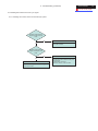
1
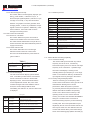
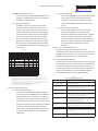
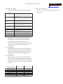
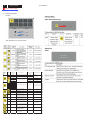
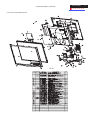
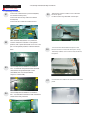
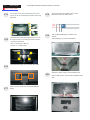
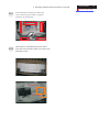
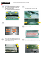
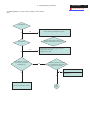
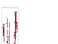
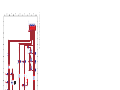
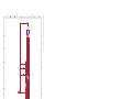
ACER
ACER_LCD_X223W_SM072301V1
Service
Model ID: R22ANUW-M1
Service Manual
Table of Contents
Important Safety Notice------------------------------------------------------------------------------------- 01
01. Product Specification--------------------------------------------------------------------------------- 02
02. OSD Menu-----------------------------------------------------------------------------------------------08
03. Exploded Diagram ------------------------------------------------------------------------------------- 10
04. Assembly and Disassembly Procedures-----------------------------------------------------------12
05. Troubleshooting----------------------------------------------------------------------------------------20
06. Schematics and Layouts------------------------------------------------------------------------------ 30
Appendix I : User’s Manual
Appendix II: Quick Setup Guide
Appendix III : Spare Parts Llist
Safety Notice
Any person attempting to service this chassis must familarize with the chassis and be aware of the
necessary safety precautions to be used when serving electronic equipment
containing high voltage.
Published by LITE-ON Service Printed in Taiwan © All rights reserved Subject to modification
23th-Jul-2007
Important Safety Notice
ACER X223W
Go to cover page
Product Anouncement:
This product is certificated to meet RoHS Directive and
! Using Lead-Free solder to well mounted the parts.
Lead-Free produced definition. Using approved critical
! The fusion point of Lead-Free solder requested in the
components only is recommended when the situation
to replace defective parts. Vender assumes no liability
express or implied, arising out of any unauthorized
modification of design or replacing non-RoHS parts.
Service providers assume all liability.
Qualified Repairability:
Proper service and repair is important to the safe,
reliable operation of all series products. The service
providers recommended by vender should being
aware of notices listed in this service manual in order
to minimize the risk of personal injury when perform
service procedures. Furtermore, the possibile existed
improper repairing method may damage equipment or
products. It is recommended that service engineers
should have repairing knowledge, experience, as well
as appropriate product training per new model before
performing the service procedures.
NOTICE:
! To avoid electrical shocks, the products should be
connect to an authorized power cord, and turn off the
master power switch each time before removing the
AC power cord.
! To prevent the product away from water or explosed
in extremely high humility environment.
! To ensure the continued reliability of this product,
use only original manufacturer’s specified parts.
! To ensure following safty repairing behavior, put the
replaced part on the components side of PWBA, not
solder side.
! To ensure using a proper screwdriver, follow the
torque and force listed in assembly and disassembly
procedures to screw and unscrew screws.
degree of 220 ° C.
1
2
ACER X223W
1. Product Specification
Go to cover page
The LCD monitor consists of an interface board , a power board
1.1 SCOPE
This document defines the design and performance
, a function key board and two speaker (1W)(with audio)
requirements for an 20/22W inch diagonal , flat panel
The interface board will house the flat panel control logic ,
monitor .The display element shall be a WSXGA
brightness control logic, audio function control (option), key
(1680x1050) resolution TFT-LCD (Thin Film Transistor
function control, DDC and DC to DC conversion to supply the
Liquid Crystal Display).16.7M color(RGB 6bits+FRC)
appropriate power to the whole board and LCD flat panel , and
images are displayed on the panel.Video input signals are
transmitting LVDS signals into LCD flat panel module to drive
analog RGB (0.7Vp-p). When the systemis powered-on ,
the LCD display circuit .
previously stored screen parameters for a pre-defined
The power board will support main power DC5V to interface
mode will be recalled if the operating mode is one of stored
board, and the power DC5.3V to audio function power of
in memory( 19 factory , 9 users timing ).This monitor
interface board,and drive the two CCFLs (Cold Cathode
operates normal by non-interlaced mode. DDC (Display
Fluorescent Tube).The interface board provides the power ON /
Data Channel) function is DDC2Bi compliance Power
OFF control over the whole monitor and control for DPMS LED
saving function complies with the DPMS (Display Power
indicator to function key board.
Management Signaling) standard.
MONITOR SPECIFICATIONS
1.2 GENERAL REQUIREMENTS
ITEM
1.2.1 Test Condition
Signal Input
SPEC
Analog :
H : 30kHz~81kHz
V : 56Hz~76Hz
Frequency
(Analog)
Brightness level & contrast level max. Full white
pattern test mode following spec. Warm up more than
Pixel clock
165MHz (Max)
1 hr, ambient light < 10 Lux , Luminance meter CA110
Video Input
Analog
Display Pixels
640 x 480 (VGA) ~ 1680 x 1050 (WSXGA)
Sync Signal
Separate SYNC for TTL (N or P)
or BM7 or same equipment .
1.2.2 Test Equipment
Signal Input
The reference signal source is a calibrated Chroma
Digital :
H : 30kHz~81kHz
Frequency
(Digital)
V : 56Hz~76Hz
Pixel clock
165MHz (Max)
Video Input
2135 video generator or higher.The use of other
0.7Vp-p
Analog
0.7Vp-p
Input Impedance 75Ω
signal generators during qualification and production
is acceptable provided the product complies with this
specification.
Connector
640 x 480 (VGA) ~ 1680 x 1050 (WSXGA)
AC100V ~ AC240V ± 10% 50/60Hz , 3 pin AC power cord
Input connector
D-SUB 15 pin & DVI-D
Audio Jack
Audio input 3.6F
(OPTIONAL)
Power Consumption
AC in 100V~240V
User's Control
Front
Empowering,Auto Adjust,Adjust(-),Adjust (+),Menu,Power
OSD
Contrast , Brightness , Position ,Clock ,Phase
,Analog/Digital,RESET, Color , Language select , Audio
(option), etc.
Factory
19
1.3 ELECTRICAL
This section describes the electricalrequirement of the
Display Pixels
AC Input
Pre-Defined Timing
monitor.The block diagram in Figure1 illustrates the various
User
Plug and Play
electrical sub-system.
Active 48W (with Audio), active 38W, power saving < 2W
9
VESA DDC2Bi
Power Saving
VESA DPMS
Input Signal Counter Tolerance
≦ H ± 1kHz, ≦ V ± 1 Hz
1.3.1 Interface Connectors
1.3.1.1 Power Connector and Cables
Figure 1
Monitor Block Diagram
The AC input shall have an IEC/CEE-22 type male
power receptacle for connection to mains power.
CCFT Drive
LCD Flat Panel
Panel data & control, DC power
The power cord shall be with length of 1.8+/-0.005
meters.
Power Board
1.3.1.2 Video Signal Connectors and Cable
DC 5V
DC 5.3V (Audio)
AC to DC Adapter,
DC to DC Converter,
DC to AC Inverter.
Inverter control
Speaker line input
Audio Source
shielded,triple row, 15 position, D-subminiature
Host Computer
Function key input
AC - IN
Audio line input
(Option)
At the end of the cable shall be a molded-over,
Audio
AM P.
(Option)
Video Signal input & DDC
1W*2
Speaker
The signal cable shall be 1.8 +/-0.005 meters long.
Interface Board
Flat Panel Controller, DDC
Function
Key Board
connector. The CPU connection shall have captive
screw locks, which will be adequate for hand
tightening. The monitor connection may use small
screws.
1. Product Specification (continued)
ACER X223W
3
Go to cover page
C o n n e c to r
P in
1.3.2.1 Video Signal Amplitudes
A s s ig n m e n t
D SU B
P in
S ig n a l
P in
S ig n a l
P in
S ig n a l
The three video inputs consist of Red ,Green , and Blue
1
R e d -V id e o
6
R e d -G N D
11
N C
2
G re e n -V id e o
7
G re e n -G N D
12
D D C -S D A
signals, each with its own coaxial cable terminated at the
3
B lu e -V id e o
8
B lu e -G N D
13
H -S Y N C
monitor. These video signals are analog levels, where 0
4
5
N C
D D C -G N D
9
10
+5V
S y n c -G N D
14
15
V -S Y N C
D D C -S C L
V corresponds to black , and 700 mV is the maximum
signal amplitude for the respective color, when each
C o n n e c to r P in D e s c rip tio n
D -S U B P in D e s c riptio n
P in
N ame
1
R e d - V id e o
2
G re e n- V id e o
3
B lue - V id e o
4
GN D
5
DDC -GN D
6
Red-G N D
7
G re e n- G N D
8
B lue - G N D
9
+5V
10
S ync - G N D
11
GN D
12
DDC _SDA
13
H-SYN C
14
V-SYN C
15
DDC -SC L
D e s c riptio n
R e d vid e o signa l inp ut.
G re e n vid e o signa l inp ut.
B lue vid e o signa l inp ut.
G ro und
D D C gro und fo r the V E S A D D C 2 B i func tio n.
A na lo g signa l gro und fo r the R e d vid e o .
A na lo g signa l gro und fo r the G re e n vid e o .
A na lo g signa l gro und fo r the B lue vid e o .
+ 5 V inp ut fro m ho st syste m fo r the V E S A D D C 2 B i func tio n.
S igna l gro und
G ro und
S D A signa l inp ut fo r the V E S A D D C B 2 i func tio n.
H o rizo nta l signa l inp ut fro m the ho st syste m .
V e rtic a l signa l inp ut fro m the ho st syste m .
S C L signa l inp ut fo r the V E S A D D C 2 B i func tio n.
signal is terminated by a nominal 75.0 ohms .For a given
monitor luminance levels are measured using this
defined video amplitud driving a monitor meeting the
termination requirements .The signal amplitude is not to
be readjusted to compensate for variations in termination
impendance.
1.3.2.2 Video Signal Termination Impedance
This analog video signal termination shall be 75Ω+/-1%
which shall be resistive with a negligible reactive
component .
DVI-I / DVI-D (If using DVI-D cable, C1, C2, C3, C4, C5 is NC)
Pin
1
2
3
4
5
6
7
8
9
10
Signal
Pin
11
12
13
14
15
16
17
18
19
20
RX2RX2+
GND
NC
NC
SCL
SCA
Analog V-Sync (NC)
RX1RX1+
Signal
GND
NC
NC
5V
GND
HP
RX0RX0+
GND
NC
Pin
21
22
23
24
C1
C2
C3
C4
C5
Signal
NC
GND
RXC+
RXCAnalog Red (NC)
Analog Green (NC)
Analog Blue (NC)
Analog H-Sync (NC)
GND
Name
RX2RX2+
GND
NC
NC
SCL
SDA
high or active low, depending upon the timing .The
Vertical Sync (VS) TTL signal is used to initiate the
display of a new frame .VS may be either active high or
active low, depending on the timing
The monitor must accept sync signals from both 3.3 and
Description
TMDS link #0 channel#2 differentialpair
TMDS link #0 channel#2 differentialpair
GNDfor no link share
NC
NC
Clock line for DDC interface
Data line for DDC interface
Analog
V-sync for analoginterface
8
V-Sync
9 RX1- TMDS link #0 channel#1 differentialpair
10 RX1+
TMDS link #0 channel#1 differentialpair
11 GND
GNDfor no link share
12 NC
NC
13 NC
NC
14 5V
+5Vinput fromhost systemfor DDC2Bfunction.
15 GND
Ground(Usingas Detect Cable)
Pin
16
17
18
19
20
21
22
Name
HP
RX0RX0+
GND
NC
NC
GND
Description
Hot plugging
TMDS link #0 channel#0 differentialpair
TMDS link #0 channel#0 differentialpair
GNDfor no link share
NC
NC
Clock shield
5 volt TTL logic families.The inputs shall sense a logic 0
when the input is 0.8 volt or less and shall sense a logic
1 when the input is 2.0 volts or greater. In addition to
these level requirements, there shall also be a minimum
23 RXC+
TMDS clock differentialpair
of 0.3 volt hysteresis provided for noise immunity
24 RXCAnalog
C1
Red
Analog
C2
Green
Analog
C3
Blue
Analog
C4
H-Sync
Analog
C5
GND
TMDS clock differentialpair
(typically by using a Schmitt Trigger input ).That is , the
AnalogRed signal
AnalogGreensignal
AnalogBlue signal
H-sync for analoginterface
AnalogGND
1.3.1.3 Audio Jack (option)
This jack shall connect the audio input from host
computer.
1.3.2 Video Input Signals
Video Input Signal
No.
1
2
3
4
5
Note
The Horizontal Sync (HS) TTL signal is used to initiate
the display of a horizontal line. HS may be either active
1.3.2.4 Sync Signal Levels
DVI-I / DVI-D ConnectorPinDescription
Pin
1
2
3
4
5
6
7
1.3.2.3 Synchronization ( Sync ) Signals
Symbol
Item
Min Normal Max Unit
Remark
Fh
Scanning Horizontal Frequency
30
81 kHz
Minimum range
Fv
Scanning Vertical Frequency
55
76 Hz
Minimum range
Vih
Hi Level Input
2.0
5.0 V
Note 1)
Vil
Low Level Input
0
0.8 V
Note 1)
Video
RGB Analog Video Level
0.0
0.7
1.0 V
75Ω to Ground
1) Schmitt-Triggers Input , Supported 3.3V device H(&V) sync output from PC.
input level at which the monitor actually detects a logic 0
shall be at least 0.3 volt lower than the level at which it
actually detects a logic 1.If the monitor sync processing
circuits are designed around the 3.3 volt logic family
,then the sync inputs must be 5 volt tolerant .
1.3.2.5 Sync Signal Loading
TTL input loading shall be equivalent to one TTL input
load. When logic 0 is asserted by a sync input , the
maximum current source from any single monitor sync
input to the driver is 1.6 mA .When logic 1 is asserted ,
the maximum current source from the driver to any
single monitor sync input is 400 uA .
ACER X223W
4
1. Product Specification (continued)
Go to cover page
1.3.2.6 Abnormal Signal Immunity
1.3.3.4 OSD adjustment
The monitor shall not be damaged by improper sync
timing , pulse duration , or absence of sync , or
ITEM
abnormal input signal amplitude ( video and/ or sync
too large or too small) , or any other anomalous
behavior of a graphics card video generator when
CONTENT
AUDIO VOLUME
To increase or decrease the sound level
BRIGHTNESS
Back light Luminance of the LCD panel is adjusted.
CONTRAST
A gain of R , G and B signal is adjusted.
changing modes , or when any combination of input
AUTO CONTRAST
A gain of R , G and B signal auto adjust.
signals is removed or replaced . Additionally , under
CLOCK
The ratio of dividing frequency of the dot clock is adjusted.
these conditions , the monitor shall not cause
PHASE
The phase of the dot clock is adjusted.
damage to the driving source
H-POSITION
The indication screen is horizontally moved right and left (1 Pixels pitch).
V-POSITION
The indication screen is vertically moved up and down (1 Pixels pitch).
AUTO ADJUST
Clock system auto adjustment, about under 8 sec.
COLOR BALANCE
Select three kinds of modes. ( USER /6500 / 9300 ).
The monitor shall have a power control switch
OSD POSITION
The OSD indication position can be adjusted.
visible and accessible on the front of the monitor .
OSD LANGUAGE
Select the language used for the OSD menu among English , French ,
Italian , Deutsch and Spanish.
1.3.3 User Controls and Indicatiors
1.3.3.1Power On / Off Switch
The switch shall be marked with icons per IEC 417 ,
RECALL DEFAULTS All data copy from factory shipment data.
# 5007 and # 5009.The switch shall interrupt the DC
supply to the monitor
1.3.3.2 Power Indicator LED
The monitor shall make use of an LED type
indicator located on the front of the monitor .
OSD DURATION
Adjust OSD menu off time range from10~120 second.
POWER-SAVE
Back light of the LCD panel is cut when the signal is not input (AC line
power consumption 2W or less).
INFORMATION
The frequency of the horizontal / vertical synchronizing signal under the
input is indicated.
※ NOTE : OSD MENU SEE APPENDIX A
The LED color shall indicate the power states as
given in Table 1.
1.3.4 Monitor Modes and Timing Capability
1.3.4.1 Format and Timing
Table 1
Function
LED Color
Full Power
Blue color
Sleep
Orange color
1.3.3.3 On-Screen Display
The monitor shall synchronize with any vertical
frequency from 55 to 76 Hz , and with any
horizontal frequency from 30 to 81KHz. If the input
frequency is out of the above – specified range,
the monitor shall display a warning screen
indicating that the input frequency is out of range.
The Lite-ON On Screen Display system shall be
Under no circumstances shall any combination of
used , controlled by a Menu button. If the buttons
input signals cause any damage to the monitor .
remain untouched for OSD turn off time while
1.3.4.2 Factory Assigned Display Modes
displaying a menu , the firmware shall save the
There are 19 factory pre-set frequency video
current adjustments and exit. Also, if the video
modes. These modes have a factory pre-set for all
controller changes video mode while the OSD is
characteristics affecting front-of-screen
active, the current settings shall be saved
performance. When the system is powered-
immediately, the OSD turn off, and new video mode
on,previously stored screen parameters for a pre-
is displayed.
defined mode will be recalled if the operating
mode is one of those stored in memory. If the
Description
Key
MENU
When no OSD display OSD Displayed
Menu Display
1. To display the OSD menu on the screen.
2. To select the OSD sub-Menu
>
Speaker Volume/Minus 1. Forward selection of the OSD menu.
(with Audio)
2. Increase the value after sub-menu selected.
<
Speaker Volume/Plus
(with Audio)
1. Back-forward selection of the OSD menu.
2. Decrease the value after sub-menu selected.
Auto
Auto Adjust Function
Menu or sub.menu EXIT/Auto Adjust function.
Empowering
Menu or sub.menu EXIT/Scenario mode
E
operating mode is not one of those stored in
memory, the monitor CPU will select the PRESET
timing for a mode that is the next lowest in
horizontal scanning frequency to the mode being
currently used. The screen parameters may be
adjusted by the use of the front bezel controls and
then may be saved as a user defined mode. The
monitor shall include all the preset video timings
shown in the following page.(Please see Note.(3) )
ACER X223W
1. Product Specification (continued)
5
Go to cover page
1.3.4.3 Mode Recognition Pull-in
1.3.5.2 Video Stretching
The monitor shall recognize preset modes within a
The monitor shall contain provisions to “stretch” the
range of +/-1KHz whichever is less for horizontal ;
video signal, so that an input signal from the
and within +/-1Hz for vertical.
computer in any resolution smaller than 1680 x
1050 is automatically expanded to fill the entire
1.3.4.4 User Display Modes
screen.
In addition to the factory pre-set video modes,
provisions shall be made to store up to 9 user
modes. If the current mode is a user mode, the
The controller supplied with the monitor shall
monitor shall select its previously stored settings.
control all panel timing. This controller shall
If the user alters a setting, the new setting will be
adequately insulate the monitor from the computer,
stored in the same user mode. The user modes
so that no possible combination of input signals
are not affected by the pre-set command. If the
from the computer shall cause damage to the flat
input signal requires a new user mode, storage of
panel or any other component of the monitor. The
the new format is automatically performed during
LCD panel interface shall support the TFT
user adjustment of the display (if required, please
standard.
1.3.6 DC - AC Inverter Requirements
see Note.(4) )
The DC-AC inverter is on the power board. The
Preset T im ing C hart
Polarity
H
V
+
-
720 x 400 (70H z)
640 x 480 (59.94H z)
640 x 480 (66.66H z)
H -Sync
(K H z)
31.469
31.469
35
B and W idth
(M H z)
28.322
25.175
30.24
640 x 480 (72H z)
640 x 480 (75H z)
37.861
37.5
31.5
31.5
-
-
648 x 500 (57.7H z)
31.234
25.175
+
+
Item
No
R esolution
1
2
3
102
103
182
4
5
173
109
6
1.3.5.3 Panel Timing and Interface
7
104
800 x 600 (56.25H z)
35.156
36
+
+
8
116
800 x 600 (60H z)
37.879
40
+
+
9
117
800 x 600 (72H z)
48.077
50
+
+
10
110
800 x 600 (75H z)
46.875
49.5
+
+
11
108
832 x 624 (74.55H z)
49.722
57.28
12
118
1024 x 768 (60H z)
48.363
65
13
157
1024 x 768 (70H z)
56.476
75
14
141
1024 x 768 (75H z)
60.023
78.75
+
+
15
126
1152 x 864 (75H z)
67.5
108
+
+
16
161
1280 x 960 (60H z)
60
108
+
+
17
179
1280 x 1024 (60H z)
63.981
108
+
+
18
131
1280 x 1024 (75H z)
79.976
135
+
+
19
1680 x1050(60H z)
65.3
146.25
+
N O TE : (1) 76 ≦ FV ≦ 86 : m onitor can display but doesn't guarantee.
(2) fV < 55, or fV > 86 : w arning invalid m ode.
(3) Factory m odel :
A fter w e first burn the code into the flash, every preset-m odel w e run first m ust do auto-adjusting.
Then it'll not do auto-adjust again w hen w e changed preset-m ode back including A C on/off D C on/off.
The only w ay that preset-m ode do auto-adjust again is press '' Internal Factory R eset''.
(4) U ser m ode :
The code should m em orize 9 tim ing m ode exclusive of preset-m odes as use m ode and do auto-adjusting.
W hen user set a new m ode that is not am ong previously. It'll do auto-adjusting then be solved to user m odes.
The new m ode w ill overw rite the first m em orized user m odes.
The user m odes be cleared is sam e as Factory m ode. Just do '' Internal Factory R eset''.
(5) Internal Factory R eset and O SD Factory R eset behavior.
frequencies used by the DC-AC inverter used to power the
backlight shall be chosen so as to prevent any noticeable
effects on the flat panel (such as a rolling effect).
1.3.7 Power Supply Requirements
The AC to DC converter power supply for the monitor shall
be an external AC to DC converter ”brick” This brick shall
have an IEC receptacle for main power input and a pin - in
-socket for DC power out. The brick shall provide sufficient
power for both the monitor and the backlight assembly,
and shall meet requirements specified in Table 2.
Table 2
AC to DC Converter Requirements
Input Voltage Range
The operating range shall be from 90 to 132 and 195 to 265 AVC
sinusoidal for all models specified.
Input Frequency Range
Input power frequency range sha;; be from 47.5 to 63 Hz over the
specified input voltage range.
Power Consumption
Power consumption for the monitor shall be less than 46W over the
specified voltage and frequency ranges. In suspend or sleep mode
the power consumption will be less than 2W.
Line Fuse
The AC input shall be fused and become electrically open as a result
on an unsafe current level. The fuse many not be user replaceable.
Initial Cold Start
The power supply shall start and function properly when under full
load, with worst case conditions of input voltage, input frequenct,
operating temperature, and cold backlight lamps.
Inrush Current
The inrush current must be limited to 30A when operated at
120VAC, and 50A when operated at 220VAC. Inrush current is
measured at an ambient temperature of 25oC, with the unit
temperature stabilized in the power-off.
Hot Start Cycle
The power supply shall be damaged when switched ON for one
second and OFF for one second for seven consecutive after
operating for one hour at full load, 25 oC, and nominal input line
voltage.
Under Voltage
The power supply shall contain protection circuitry such that the
application of an input voltage below the minimum specified in this
table shall not cause damage to the power supply unit nor cause
failure of the input.
Line Transient
The power supply shall operate within IEC 801-4 (± 1KV) and IEC
801-5 (± 2KV) for the domestic U.S. version. The UPS power
supply shall operate and comply with CE mark.
1.3.5 Controller Requirements
1.3.5.1 General Requirements
The monitor shall include a controller capable of
converting the analog RGB signal from a standard
SXGA resolution video controller in the CPU to a
signal which can be displayed on the panel. The
controller will include a PLL, A/D converters, LVDS
transmitter and other circuitry necessary to perform
its function. The PLL shall be stable enough to
ensure that a static image from the CPU is placed
in the same physical location on the flat panel in
each frame.
6
ACER X223W
1. Product Specification (continued)
Go to cover page
1.3.8 Display Communications Channel
1.4.4.2 Lamps Startup Time
The monitor assembly shall provide a display
The backlight lamps shall start about 2 sec of the
communications channel that conforms to VESA
time the monitor power switch is pressed or the
DDC2Bi hardware requirements. This configuration
monitor is restarted from a power - down mode .The
shall contain the 128-byte EDID file as specified by
starting time shall stay about 2 sec. for the
VESA EDID standard.The monitor should not write to
minimum expected life of the lamps.
the EDID file for the first two minutes of operation
Test conditions are as follows :
following power-up UNLESS some action taken by the
Ambient Light ----------------------
< 1.0 lux
user or the host CPU forces the write (for instance,
Temperature--------------------------
10℃
Inactive Time -----------------------
> 24 hours
requesting the serial number via the OSD).
Furthermore, it is recommended that CMOS switches
be incorporated to isolate the DDC IC from outside
1.4.5 Defects
1.4.5.1 Visual Inspection
connections while the EDID Fault Management is
The LCD panel shall be inspected with all pixels set
being updated. This is to prevent corruption of the data
to white,black , red , green , and blue. The color
by attempts to read the data while it is being changed.
variation, brightness variation , and overall
1.3.9 Firmware Update Function (same ISP function)
appearance must not be perceived as poor quality
The update firmware need through from the D-Sub
by Lite-On . Areas and / or parameters considered
connector, use DDC I2C bus to do update firmware.
questionable shall be subjected to detailed
1.4 PANEL ELECTRICAL
1.4.1 General Requirements
measurements .
1.4.5.2 Display Degradation
The panel used as the display device shall be an
Over the life of the product , variation of the
WSXGA resolution,20/22W, TFT-LCD.This panel shall
parameters specified in Panel specification shall be
be approved for use in this monitor.
maintained within reasonable limits.The panel must
1.4.2 Panel Timings
not exhibit any significant defects while in operation
The controller included with the monitor shall translate
( excluding the CCFL operation ).This does not in
all video timings from the CPU that meet the timing
any way change the warranty given by the panel
requirements listed in Panel specification into timings
manufacturer .
appropriate for the panel. Under no circumstances may
1.4.5.3 Light Leakage
the controller supply the panel with timings that may
Except for the active display area , there shall be no
result in damage. The controller shall insulate the
light emission visible from any angle from any other
panel from the CPU , so that the panel shall always be
part of the display . For this test , the ambient
driven per it's own specification regardless of the
illumination must follow panel's specification.
timings being sent from the CPU.
1.4.3 Polarizer Hardness
1.4.5.4 Allowable Defects
No cosmetic defects are allowed except those
The outer face of the front polarizer panel shall be
specified below.The conditions of visual inspections
covered with a coating with a # 3 hardness value .
are as follows :
1.4.4 Backlight Requirements
For P20/22 W Series.
1.4.4.1 General Requirements
■Viewing distance is to be approximately 35-50cm
The backlight assembly shall be designed to support
field replacement at the customer site or authorized
■Ambient illumination is to be 300 to 700 lux.
service center. The lamps shall have a continuous
■Viewing angle shall be at 90 degree.
operating life of at least 40,000 hours at 25. The
■Defects not apparent within one minute shall be
operating life is defined as having ended when the
illumination of light has reached 50% of the initial
value. The lamps shall extend a sufficient amount
from the edge of the light guide that sputtering over
the life of the lamps shall not cause degradation of
the luminance uniformity (such as non-illuminated
bands along the edges of the display).
ignored.
1. Product Specification (continued)
ACER X223W
7
Go to cover page
1.4.5.5 Defect Terminology
1.5
Optical Characteristics
Table 3 gives the descriptive terms used in classifying
Depends on the LCD supplier's spec. Details refer to QA
defects.
Inspection Spec.
D ark / Spots / Lines
Spots or lines that appear dark in the display patterns and are
usually the result of contam ination. D efects do not vary in
size or intensity (contrast) w hen contrast voltage is varied.
C ontrast variation can be achieved through the use of varying
gray shade patterns.
Bright Spots / Lines
Spots or lines that appear light in the display patterns.
D efects do not vary in size or intensity (contrast) w hen
contrast voltage is varied. C ontrast variation can be achieved
through the use of varying gray shade patterns.
Polarizer Scratch
W hen the unit lights, lines appear light (w hite) w ith display
patterns dark and do not vary in size. Physical dam age to the
polarizer that does not dam age the glass
Polarizer D ent
W hen the unit lights, spots appear light (w hite) w ith display
patterns dark and do not vary in size. Physical dam age to the
polarizer that does not dam age the glass.
R ubbing Line
N ew ton R ing
H orizontal or diagonal lines that appear gray w ith the display
patterns dark and m ay have resulted from an “out of control”
rubbing process on the polyim ide or “w aves” on the B EFs or
prism sheets.
The “rainbow ” effect caused by non-uniform cell thickness.
W hen the unit lights, variation / non – uniform ity
(splotchiness) appears light (w hite) w ith the display and
m ight vary in size.
W hen the unit lights, line(s) in the m onitor (vertical) or m ajor
(horizontal) axis appear dim , but not com pletely on or off.
M ottling
D im Line
C ross Lines O ff
W hen the unit lights, lines in both the m inor and m ajor axis
do not appear.
Bright / D ark D ot
A sub – pixel (R ,G ,B dot) stuck off / on (electrical).
1.4.5.6 Smudges, Streaks and Smears
When viewing the panel oriented so as to maximize
reflected light , there shall be no visible smudging ,
streaking, smearing or other nonuniformity from
contaminants ,fingerprints,or defects in any of the visible
surfaces. This is independent of whether the unit is
operating or off .
1.4.5.7 Other Defects
Undefined defects that are considered to be rejectable
by Lite–On will be reviewed by Lite-On as they become
apparent. These panels will be referred to the Lite - On
Corporate / Manufacturer Purchasing Agreement for
disposition.
1.4.5.8 LCD Inspection
Put LCD panel on inspection table and illuminate the
panel with a daylight fluorescent lamp located above the
panel surface such that the illuminance at the LCD panel
is between 1000 lux and 1500 lux .Defect limits are given
in Table 4 .
Average Diameter smaller of
(L+W)/2 or L/20+2W
Acceptable Number
Minimum Separation
< 0.1mm
Non countable
N/A
0.1 mm ~ 0.3 mm
10
15 mm
0.31 mm ~ 0.5 mm
10
15 mm
0.51 mm ~ 1.25 mm
5
15 mm
1.26 mm ~ 2.5 mm
3
25.4 mm
2.51 mm ~ 3.75 mm
3
25.4 mm
Greater than 3.75 mm
NONE
Not applicable
Note : Allowable distance between spots of two sizes is the minimum separation
number for the smaller spot. Therefore, if there are two spots, 1.30mm and 0.4mm
in diameter, they must be at least 15mm apart.
ACER X223W
8
2 OSD Menu
Go to cover page
2.1 MAIN OSD MENU
Outline:
The description for control function:
M a in
M enu
Ic o n
Sub
Menu
Ic o n
Sub Menu
Ite m
N /A
W a rm
N /A
Cool
D e s c r ip t io n
S e t t h e c o lo r t e m p e r a t u r e t o
w a r m w h it e .
S e t t h e c o lo r t e m p e r a t u r e t o
c o o l w h ite .
U s e r /R e d
U s e r /G r e e n
A d ju s t s R e d /U s e r /G r e e n
G r e e n /B lu e in t e n s it y .
U s e r /B lu e
N
N
N
N
N
N
N
N
/A
/A
/A
/A
/A
/A
/A
/A
E n g lis h
D e u ts c h
F r a n c a is
E spanol
Ita lia n o
H . P o s it io n
V.
P o s it io n
OSD
T im e o u t
N /A
A u t o C o n f ig
N /A
A n a lo g
N /A
D ig it a l
N /A
D D C /C I
s w itc h
N /A
In f o r m a tio n
N /A
R eset
N /A
E x it
M u lti- la n g u a g e s e le c tio n .
A d ju s t t h e h o r iz o n t a l
p o s it io n o f th e O S D .
A d ju s t t h e v e r t ic a l p o s it io n
o f th e O S D .
A d ju s t t h e O S D t im e o u t.
A u t o A d ju s t th e H /V
P o s itio n , F o c u s a n d
C lo c k o f p ic tu r e .
( O n ly A n a lo g In p u t M o d e l)
S e le c t in p u t s ig n a l fr o m
a n a lo g (D -S u b )
( O n ly D u a l In p u t M o d e l)
S e le c t in p u t s ig n a l fr o m
d ig it a l ( D V I)
( O n ly D u a l In p u t M o d e l)
S e le c t th e D D C /C I O N o r
OFF
S h o w t h e r e s o lu t io n , H /V
f r e q u e n c y ,S N a n d
in p u t p o r t o f c u r r e n t in p u t
t im in g .
C le a r e a c h o ld s ta tu s o f
A u t o - c o n f ig u r a tio n
a n d s e t th e c o lo r
te m p e r a tu r e to W a r m .
S a v e u s e r a d ju s tm e n t a n d
O S D d is a p p e a r .
A d ju s tm e n t
R ange
N /A
N /A
R e s e t V a lu e
T h e c o lo r
t e m p e r a t u r e w ill b e
s e t to c o o l.
0 -1 0 0
100
0 -1 0 0
100
0 -1 0 0
100
N /A
T h e la n g u a g e w ill
b e s e t t o E n g lis h
0 -1 0 0
50
0 -1 0 0
50
1 0 -1 2 0
10
N /A
N /A
N /A
N /A
N /A
N /A
N /A
T h e D D C /C I s w itc h ,
d e f a u lt is “ O N ” in
m o n ito r .
N /A
N /A
N /A
N /A
N /A
N /A
2. OSD Manu (continued)
ACER X223W
Go to cover page
9
10
ACER X223W
Go to cover page
3.1 Packing Exploded Diagram
3. Exploded Diagram
3. Exploded Diagram (continued)
ACER X223W
Go to cover page
3.2 Product Exploded Diagram
11
ACER X223W
12
4. Assembly and Disassembly Procedures
Go to cover page
4.1 Assembly procedures:
Connect the cable between power board(P802)
S1
and interface board (P301)
S5
Connect the function key cable into interface
Take the key function cable out from the hole
shown as photo
Fix the function key cable with a PVC tape
board(P306)
Connect the FFC cable into interface board
P301
P802
FFC
P306
Take a bracket chassis base on a protective
S2
cushion and stick an insulator on the specific
position, take a power board and turn it over. Then,
put it on the specific positions of bracket chassis
Turn the monitor faced down and put it on the
S6
base.
Bracket Chassis module till both parts firmly
Take lamp cables out from the holes shown as
the photo.
Use a Phillips-head screwdriver screwed the
S3
No.1~4 screws till that power board and bracket
chassis base firmly attached.(No1 screw
size=M4x8; No2~4 screw size=M3x6;
Torque=9~10KGFxCM).
3
2
S7
1
4
Use a Phillips-head screwdriver screwed the
S4
No.1~4 screws till that interface board and bracket
chassis base firmly attached.
3
4
2
1
Connect the FFC cable to the connector of the LCD
panel.
4. Assembly and Disassembly Procedures (continued)
13
ACER X223W
Go to cover page
Use a Phillips-head screwdriver screwed the No.1~4
S8
Connect FFC cable to LCD panel. There are two
locks over here when plugging in should be
S10
screws on both side and assemble the LCD panel
and bracket chassis module.
noticed
(No1~4 screw size=M3x6; Torque=3~4KGFxCM).
2
1
4
3
S7
S11
Use a Phillips-head screwdriver screwed the
No.1~2 screws.
(No1~2 screw size=M3x10; Torque=3~5KGFxCM).
1
2
Plug in parallel direction
Use a Hex-head screwdriver screwed the
S12
DVI and D-SUB connectors (No.1~4Hex Nut
screws Size=M3x8;Torque=3~5KGFxCM).
S8
1
2
Angel < 5 degrees
S9
Plug 8 lamp cables to the connectors of power
board.(Both of right and left sides)
S13
Take a key function board to hook with front
bezel (No.1~2) and connect to key function
cable.
1
2
ACER X223W
14
4. Assembly and Disassembly Procedures (continued)
Go to cover page
S14
Put a rear cover on the assembled unit and
press on force mechanisms locked and firmly
S18
Stick Vista and TC003 label on the correct
position the same as below photo
attached.
S19
Assemble the stand upper side to the rear cover
S15
Take a LDPE+EPE bag to cover the LCD
monitor.
Take a PE bag to cover the stand base.
through the way of screwing 4 screws till both
units firmly attached.
(No1~4 Screw Size=M4x10;
Torque=11~13KGFxCM).
3
4
S16
1
2
Assemble the hinge cover into both two sides
S20
Take two cushion foams; one is held the front
side of LCD monitor, and another is held the back
side.
Stick a screen card on the front bezel with two
S17
tapes.
4. Assembly and Disassembly Procedures (continued)
ACER X223W
Go to cover page
S21
Put accessories of stand, DVI cable, and
user’s manual ,power cable on specific
USER’S MANUAL
STAND
S22
DVI CABLE
POWER CABLE
positions as photo below.
D-SUB CABLE
Move previous assembled parts into the carton
then stick Vista and feature label on the carton then
packing the carton
FEATURE LABEL
VISTA LABEL
15
ACER X223W
16
4. Assembly and Disassembly Procedures (continued)
Go to cover page
4.2 Disassembly procedures
S1
S4
Open the carton with a proper tool.
Put returned unit on a protective cushion,then
remove LDPE+EPE bag.
Tear off tapes to remove the screen protector
card then turn over the LCD monitor (screen
faced down),
FEATURE LABEL
VISTA LABEL
S2
Take out all accessories including D-SUB cable
power cable, DVI cables, user’s manual, and stand
base and packing material from the carton.
(Note: It depends on whether users returning
USER’S MANUAL
STAND
S3
DVI CABLE
POWER CABLE
the accessories.)
S5
Disassemble the stand cover.
D-SUB CABLE
Take off two cushion foams
S6
Use a Phillips-head screwdriver unscrew 4 screws
to release the stand base.
(No1~4 Screw Size=M4x10;
Torque=11~13KGFxCM).
3
4
S7
1
2
Turn over the LCD monitor (screen faced up).
4. Assembly and Disassembly Procedures (continued)
ACER X223W
17
Go to cover page
Unhook the key function board from rear bezel,
S8
Place cloth on the panel where you are working
S9
disconnect the key function cable
on to protect the panel. Continuously, wedge
your finger between the front bezel and the
panel, then pry up on the front bezel to
disengage the locking mechanism.
S10
Use a Hex-head screwdriver unscrewed 4 screws to
release the DVI and D-SUB connectors
(No1~4Hex Nut screws
Size=M3x8;Torque=3~5KGFxCM).
Work your way along the front bezel to disengage
all the locking mechanism.
1
2
S11
Use a Phillips-head screwdriver unscrewed the
No.1~2 screws to lease power plug
(No1~2 screw size=M3x10; Torque=3~5KGFxCM).
1
2
ACER X223W
18
4. Assembly and Disassembly Procedures (continued)
Go to cover page
S12
Use a Phillips-head screwdriver unscrewed the
No.1~4 screws to disassemble the LCD panel
S15
and bracket chassis module.
Disconnect the FFC cable to the connector of
panel.
Use finger to push the lock according to arrow
direction then take out the FFC cable
(No1~4 screw size=M3x6; Torque=3~4KGFxCM).
1
2
4
3
Unplug 4 lamp cables (No. 1~4).
S13
S16
S14
Take out lamp cables right through the No.1 and
2 square holes and separate the bracket chassis
module and LCD panel apart.
S17
Examine the panel surface accoring to inspection
criteria. Put it aside.
Use a Phillips-head screwdriver unscrewed the
No.1~4 screws to release the interface board.
(No1~4 screw size=M3x6; Torque=9~10KGFxCM).
1
2
3
4
2
1
4. Assembly and Disassembly Procedures (continued)
ACER X223W
Go to cover page
Use a Phillips-head screwdriver unscrewed the
S18
No.1~4 screws to disassemble the power board.
(No1 screw size=M4x8; No2~4 screw size=M3x6;
Torque=9~10KGFxCM).
3
2
1
4
Disconnect the FFC, P301, and function key
S19
cables to connectors of interface board.
P802
P301
FFC
P306
19
ACER X223W
20
5. Troubleshooting
Go to cover page
5.1 No.display of screen (Screen is black, color of LED is
amber)
Does OSM display when you push
PROCEED buttom.
No
When a signal isn't being inputted, it is
indicated with "No Signal Input". it is
indicated with "Out Of Range" at the
time of the frequency that it can't be
distinguished.
Proceed "No OSM display" section.
Yes
Check if the sync signal from computer is
output and if the video cable is
connected normally.
NG
OK
Proceed "checking the resolution
change IC movement" section.
Input the sync signal of computer, or
change the cable.
ACER X223W
5. Troubleshooting (continued)
Go to cover page
5.2 Nothing display on screen (screen is black, color of LED is
blue)
Is backlight lit?
NG
Refer "Checking the backlight unit" section"
OK
Check the video cable for failure. Check
the host for output signal is all black or not.
Is backlight lit?
NG
OK
Check OSM menu is display on
screen when you push the
"PROCEED" key.
1) Change pattern of video signal output on the host.
2) Reconnect the video cable.
3) Change the video cable.
NG
Check if the LCD video signal cable
is connected between the Interface
Board and LCD module.
Failure Point
NG
OK
OK
Proceed "Abnormal sreen" dection"
Next
Page
The LCD video signal cable is
disconnected.
21
22
ACER X223W
5. Troubleshooting (continued)
Go to cover page
5.2 Nothing display on screen (screen is black, color of LED is
blue) continued
Continue
Check the 5V power
supply for P304 pin 1, 2, 3
NG
Check the I302 pin2
if voltage is 3.3V
Proceed "Checking the DC/DC
converter circuit" section.
NG
OK
Check the D326 pin1
if voltage is 1.8V
Proceed "Checking the DC/DC
converter circuit" section.
NG
OK
OK
Check the I301 pin2
if voltage is 5V
NG
Failure Point
1) FB301 is open.
2) C309, C310 is short.
OK
Check if the voltage
between I301 pin2
and pin3 is above 0.7V
Check if the Q301 pin2 of
PANELVCC_EN signal that
outputted by I305 pin85 is
High level.
NG
OK
Check the input voltage level whether
was changed when pressed function
keys on the P306 pin 4 (normal is high
level, when push buttom, generated
1.6V)
NG Failure Point
1) Printer wire between R307
and I305 pin85 is failure
2) I305 is failure.
Failure Point
I301 is failure.
OK
Failure Point
NG
1) Printed wire between Q301 pin3,
R305, R306, I301 pin1 is failure..
2) Q301 is failure.
Check if the voltage on
I305 pin 90 that is from
3.3V to 1.6V.
Failure Point
NG
OK
OK
Failure Point
Check the P304 all
LVDS signals.
I305 is failure
Failure Point
NG
OK
Failure Point
1) The LVDS cable broke between
P304 and LCD module.
2) LCD module is failure.
1) Printed wire broke between P304
and I305 LVDS signals.
2) I305 is failure.
Printed wire broke between P306
pin 4 and I305 pin 90.
5. Troubleshooting (continued)
ACER X223W
Go to cover page
5.3 Checking the back light unit
Is +22V supplied to inverter PWB ?
(by the power board)
Failure Point
NG
Power board of Inverter part failure.
OK
Check the BKLT_EN signal
of the DC input P301 pin2 at
TTL high level.
Failure Point
NG
OK
1) printed wire broke between P301
pin2, R303 and I305 pin 88.
2) I305 is failure.
Check the BKLT_ADJ signal
of the input P301 pin3 from
I305 pin86 is a PWM signal.
Failure Point
NG
OK
Failure Point
1) Back light unit of LCD module is
failure.
2) Inverter Cable is disconnected
1) printed wire broke between P301
pin3, R301 and I305 pin86.
2) I305 is failure.
23
24
ACER X223W
5. Troubleshooting (continued)
Go to cover page
5.4 Abnormal screen for VGA
Check the R, G, B video
signal from computer input on
P302 of video connector.
NG
Failure Point
OK
1) No R, G, B video signals output from
host computer, check computer.
2) Video signal cable disconnection.
Check the R, G, B input video
signals on I305 pin18, 20, 23
respectively that their level is 0.0
to 0.7Vp-p.
NG
OK
Check all LVDS signals
being output to P304 from
I305?
NG
OK
Process "Checking the
resolution change IC
movement" section.
Failure Point
In the case of the Red signal. (A Green and
Blue signal is the same path, too.)
1) Printed wire broke between P302 pin1
and I306 pin23.
2) Video cable is failure.
3) FB303,FB304, R309 is open.
4) R311 is short or open.
5) C315 is short or open.
Failure Point
Printed wire broke between I305 and P304.
ACER X223W
5. Troubleshooting (continued)
Go to cover page
5.5 Abnormal OSM display adjust problem
Check the input TTL level whether was changed
when pressed function keys on the P306 pin 4, 5
(normal is high level, when push buttom, generated
low level plus)
NG
Failure Point
1) Function key wire disconnection.
2) Function key wire is failure.
3) Function key board is failure.
OK
Check the input TTL level of I305
pin89, 90 whether was changed
when pressed function keys.
(Refer to Table 1)
NG
OK
Failure Point
I305 is failure.
Failure Point
1) Printed wire broke among P306 pin4, pin5; R369 and I305
pin90.
2) Printed wire broke among P306 pin5,R372, and I305 pin89.
3)C386,C388 ,C389,C390 are short.
25
26
ACER X223W
5. Troubleshooting (continued)
Go to cover page
5.6 Abnormal plug and play operation for VGA
Confirm the host computer
supplies DDC2B mode.
NG
OK
Failure Point
The host machine is not communicatiog in DDC2B
mode.
Check the voltage on
P302 pin9 that is power
DC 5 V.
NG
OK
Failure Point
The Video cable is failure.
Check the voltage on I303
pin8 that is power DC 5 V.
NG
Failure Point
1) Printed wire broke between I303 pin8, D308
and P302 pin9.
2) D309, C329 is short.
3) D308 is failure.
OK
Check the signal on P302
pin12, 15 that is serial data /
clock signal.
NG
Failure Point
OK
The Video cable is failure.
Check the output signal of
serial data/clock on I303
pin5, 6.
NG
Failure Point
OK
I303 is failure.
Failure Point
1) Printed wire broke among I305 pin30, pin31,
R328,R330 and P302 pin12, 15 .
2) I303 maybe failure.
3) R326, R327 are open.
4) R328 or R330 or C330 or C331 is open or
short.
5. Troubleshooting (continued)
ACER X223W
Go to cover page
5.7 Checking the interface circuit of sync signal
5.7.1 Checking the control circuit of horizontal sync pulse
Check the horizontal sync
signal on P302 pin13 TTL
level.
NG
Failure Point
OK
Video cable is failure.
Check the horizontal sync
signal on I305 pin27 TTL
level.
NG
Failure Point
OK
Failure Point
Process "Checking the resolution change IC
movement" section.
1) Printed wire broke between P302 pin13
and I305 pin27.
2) FB309, R321 are short.
3) D307 or R324 or C327 is short.
27
28
ACER X223W
5. Troubleshooting (continued)
Go to cover page
5.8 Checking the resolution change IC movement
Check +3.3V supply on I305 pin8,
pin14, pin16, pin24 , pin32, pin49,
pin56, pin75, pin98
NG
Proceed " Checking the DC/DC converter circuit" section.
NG
Proceed " Checking the DC/DC converter circuit" section.
OK
Check +1.8V supply on I305 pin
51, 66, 82, 34.
OK
Check X301 14.318MHz clock
input to I305 pin96 and pin97 at
TTL level.
Failure Point
NG
OK
1) Printed wire broke between X301 and I305 pin96, pin97.
2) C379, C380 is short or open.
3) X301 failure.
Check I305 pin 84 HWRESET
signal is low level at normal
operation.
Failure Point
NG
Check if D328 pin1 is low.
NG
1) Printer wire broke between I305 pin84
and C378
2) C78 is short.
OK
Failure Point
OK
Check I305 pin37, pin38, pin39,
pin40 SPI signal
(Same as the IIC signal).
1) Printer wire broke between I305 pin84 and C378.
2) C381 is short.
3) R358, D328 is failure
4) I305 is failure
Failure Point
NG
OK
Failure Point
I306 failure.
1) Printed wire broke between I305 pin37, pin38, pin39, pin40 and
I306 pin1, pin2, pin5, pin6.
2) I306 failure.
5. Troubleshooting (continued)
ACER X223W
Go to cover page
5.9 Checking the DC/DC converter circuit
Check the 5V is output from
P301 pin5, pin6.
OK
NG
Failure Point
1) Power wire disconnection.
2) Power board is failure.
Check the 5V is input to
I302 pin3.
NG
Failure Point
OK
1) Printed wire broke between P301 pin5,
pin6, and I302 pin3.
Check the 3.3V is output
from I302 pin2, 4.
NG
OK
Failure Point
I302 is failure.
Check the 3.3V is input to
Q305 pin1.
OK
NG
Failure Point
Printed wire broke between I302 pin2, pin4
and Q305 pin1.
Check the 1.8V is output
from D326 pin 1.
NG
OK
Failure Point
1) Printed wire broke between I302 pin 2. 4,
Q306 pin1 and I305 VCTRL pin.
2) FB311, FB312, FB313, FB314, FB315, are
open.
Failure Point
D326 is failure.
29
6. Schematics and Layouts:
AC
110/220V
Input
Power &
Invertor
Board
1
2
2
6.1 ACER_LCD_X223W_SCHEMATICS_BLOCK DIAGRAM
A
B
C
D
E
F
G
1
3
4
4
5
5
P301
Power Con.
6
VCTRL
1.8v
6
Flash EPROM
SST 25VF010A
PMC 25LV010A
I306
Q305
I302
DC-DC
5v-3.3v
Audio DC 5.3V Out (Option)
+5V
Brightness,Inv_On/Off
Backlight
3
7
8
LVDS
9
Panel Con.
P304
LCD Module
AUO M220EW01-V2/V0
M201EW02-V8/V9
CPT CLAA201WA04A
SEC LTM220M1-V0/L01
VLCD
I305
Scaler
10
R,G,B,Hs,Vs
RC
Reset
X301
XTAL
14.318MHZ
11
I303
DDC
24LC02B
12
P306
Key
Con.
12
VGA_DDC_CLK,
VGA_DDC_DAT
11
Analog
Video
Input
P302
Digital
Video
Input
P303
10
D-SUB
9
DVI-D
TMDS
TSUMU58BWHL-LF
I304
DDC
24LC02B
8
DVI OPTION
DVI_DDC_SCL,
DVI_DDC_DAT
7
PCB No.
13
Function
Key
Board
13
6832190100P01
A
B
C
D
E
F
G
ACER X223W
Go to cover page
30
L
G
1
3
1
F801
2.5AL250V
R802
SCK103
2
T802
LINE FILTER
R801
C801
0.33U/275V
I801
3
C820
1000P/250V
7
2
6
8
C807
10UF/50V
BEAD
L809
C819
0.22U/275V
6.2 ACER_LCD_X223W_SCHEMATICS_POWER BOARD
A
2
1M
1/4W
MGF
C808
1
SG5841J
3
1000P/250V
5
4
+
7
6
5
4
3
2
1
BRI
C812
1000P
GND-1
ON_OFF
10K
R113
R102
30.1K 1%
8
GND
ZD801
22D
4
D807
RL206
1
D805
RL206
4
2
GND
C106
0.047uF
+
5
D808
RL206
6
R824
33K 1%
GND
6
C108
220P
R818
0.51/1W
R829
NA
7
R812
100K/2W
1
7
3
4
1
D801
X
2
5
GND-1
T801
ER28
Q105
C945 22 MOF
R131
Q106
A733
GND
D804
1N4937
L803
BEAD/6mm
C810
100P
1KV X7R
R811
0.39/2W
R134
1K
R132
1K
GND-1
GND
Q104
2N7000
R830
243K
D803
1N4007
C806
0.01U/1KV
R133
22 MOF
Q803
7N65C
R807
3.3
R804
+
C805
2M
100U/450V 1/4W
MGF
GND-1
D806 1N4148
1
2
C830
4700P/1KVX7R
D812
RL206
R814
C104
330P
R107
6.8K
R118
31.6K 1%
33.2K 1%
R827
C827
0.01UF/PEM
R823
270
R813
100/MOF
1K
R825
150K 1%
R106
GND
I803
AP431 1%
22/MOF
R826
1K
+
R104
510K 1%
GND
GND
GND
C828
4.7U/50V
3
9
10
11
12
13
14
15
16
I802
LTV817
R815
200/MOF
C809
4700P/1KVX7R
C825
1000P/250V
+
GND-1
C811
220P
DRV2
PGND
I101
DRV1
CT
GNDA
VDDA
TIMER
DIM
SSTCMP
LCT
ISEN
VSEN
ENA
NC
OVPT
NC
C103
2.2uF/50V
GND
2
3
N
P801
GND
R808
30.1K 1%
+5V
R105
20
C101
0.1uF
R103
30.1K 1%
OZ9938
GND
1
4
2
3
1
R833
30.1K 1%
C110
1
+
GND
C132
1000P
5
10
9
8
7
6
GND
8
R831
X
C816
1000P
4
3
2
1
4
3
2
1
GND
2
9
D2
D2
D2
+
C134 +
10
C851
0.1UF
+5V
T101
D105
D104
1N4148
1
2
T102
7
2
7
D107
1N4148
1
2
1N4148
1
D811
24C
GND
GND
GND
5V
5V
5V
5V
BRI
ON_OFF
GND
R817
1K
BRI
GND
R126
3.65K 1%
R125
3M 1/4W
C123
10P/6KV
C109
0.022UF
X7R
GND
R115
3.65K 1%
R116
3M 1/4W
C117
10PF/6KV
GND
ON_OFF
11
4
5
6
10
EEL19-B
1
2
3
+
C823
1000UF/16V
GND
R137
100K
2
1
2
3
11
4
5
6
10
EEL19-B
D109
2
D110
1N4148
1
2
1N4148
1
1N4148
D108
1
R138
100K
R140
100K
R139
100K
R120
13K
GND
GND
10
C817
330U/35V
GND
L802
10U
+
C824
1000UF/16V
C127
+
7
330UF/35V
+
C128
330UF/35V
6
+
330UF/35V
GND
C135
330UF/35V
5
7
8
5
6
8
GND
+
C818
330U/35V
GND
+
C822
1000UF/16V
Q107
S2
D2
S2
D1
D1
D1
AOP609
G2
G1
G2
D1
GND
R130
402 1%
S1
9
C131
0.022UF
X7R
G1
AOP609
Q108
S1
GND
100V X7R
C821
1000P
500V X7R
D809
ER1002FCT
+
C129
220UF/35V
+
D810
SB1060F
R832
X
+22V
GND
GND
D113
1N4148
1
D112
1N4148
1
GND
C130
220UF/35V
R128
13K
2
8
1
2
1
2
C133
1000P
GND
4
3
1
2
R136
10K
2
C102
22uF/50V
2.2uF/50V
GND
C111
1000P
GND
R135
1M
GND
3
1
B
R101
10K
C105
1000P
GND
2
2
C
D
E
F
G
1
12
R828
51K
GND
P802
1
2
3
4
5
6
7
8
9
10
R117
100K 1%
R119
13K 1%
R122
13K 1%
R121
100K 1%
GND
R111
402 1%
1
F101
3A
C116
5PF/3KV
C115
470P
X7R
GND
2
2
1
2
1
2
1
2
1
1
2
1
2
1
2
1
GND
C113
0.1UF
13
+22V
GND
D103
1N4148
2
GND
C114
0.1UF
D115
1N4148
GND
13
P101
2P
P102
2P
P103
2P
P104
2P
6832192600P01
D102
1N4148
1
C125
5P/3KV
C120
470P
X7R
GND
2 D114
1N4148
12
PCB No.
1
2
1
2
1
2
1
2
1
2
1
2
1
2
1
2
A
B
C
D
E
F
G
ACER X223W
Go to cover page
31
VDD
VLCD
1
VCC5V
VCC5V
VCC5V
VCC3V3
VLCD
VCC5V
POWER
VCC5V
VDD
3
DDC_WPn
RX2+
RX2RX1+
RX1RX0+
RX0RXC+
RXC-
HDCP_CTRLn
DVI_DETn
DVI_DDC_DAT
DVI_DDC_CLK
3
PANELVCC_EN
VCC3V3
VLCD
2.POWER
2
BKLT_EN
BKLT_ADJ
4.DVI & DDC INTERFACE
VCC5V
DVI & DDC INTERFACE
3.VGA & DDC INTERFACE
DDC_WPn
VGA_DDC_DAT
VGA_DDC_CLK
VGA_DETn
RIN
GNDR
GIN
GNDG
SOG
BIN
GNDB
HSYNC
VSYNC
VGA & DDC INTERFACE
2
6.3 ACER_LCD_X223W_SCHEMATICS_INTERFACE_TOP
A
B
C
D
E
F
G
1
RIN
GNDR
GIN
GNDG
SOG
BIN
GNDB
HSYNC
VSYNC
VGA_DETn
4
VGA_DDC_DAT
VGA_DDC_CLK
DDC_WPn
DDC_WPn
RX2+
RX2RX1+
RX1RX0+
RX0RXC+
RXC-
HDCP_CTRLn
DVI_DETn
VCC5V
DVI_DDC_DAT
DVI_DDC_CLK
VCC3V3
BKLT_EN
BKLT_ADJ
PANELVCC_EN
4
5
6
SCALER TSUMU58BWHL-LF
RIN
GNDR
GIN
GNDG
SOG
BIN
GNDB
HSYNC
VSYNC
VGA_DETn
VGA_DDC_DAT
VGA_DDC_CLK
DDC_WPn
RX2+
RX2RX1+
RX1RX0+
RX0RXC+
RXC-
HDCP_CTRLn
DVI_DETn
DVI_DDC_DAT
DVI_DDC_CLK
VCC5V
VCC3V3
BKLT_EN
BKLT_ADJ
PANELVCC_EN
6
5.SCALER TSUMU58BWHL-LF
5
7
7
8
8
9
LVACKP
LVACKM
LVA0P
LVA0M
LVA1P
LVA1M
LVA2P
LVA2M
LVA3P
LVA3M
LVBCKP
LVBCKM
LVB0P
LVB0M
LVB1P
LVB1M
LVB2P
LVB2M
LVB3P
LVB3M
LED_G
LED_A
ADC1_IN
ADC2_IN
VOLUME
AUDIO_EN
9
LVACKP
LVACKM
LVA0P
LVA0M
LVA1P
LVA1M
LVA2P
LVA2M
LVA3P
LVA3M
LVBCKP
LVBCKM
LVB0P
LVB0M
LVB1P
LVB1M
LVB2P
LVB2M
LVB3P
LVB3M
LED_G
LED_A
ADC1_IN
ADC2_IN
10
AUDIO_EN
VOLUME
10
11
12
VCC3V3
VLCD
PANEL & KEY INTERFACE
LVACKP
LVACKM
LVA0P
LVA0M
LVA1P
LVA1M
LVA2P
LVA2M
LVA3P
LVA3M
LVBCKP
LVBCKM
LVB0P
LVB0M
LVB1P
LVB1M
LVB2P
LVB2M
LVB3P
LVB3M
LED_G
LED_A
ADC1_IN
ADC2_IN
12
VDD
6.PANEL & KEY INTERFACE
AUDIO
AUDIO_EN
VOLUME
7.AUDIO
11
PCB No.
13
VLCD
VDD
13
VCC3V3
6832190100P01
A
B
C
D
E
F
G
ACER X223W
Go to cover page
32
P301
1
2
TP1
BACKLIGHT_ADJ
BACKLIGHT_EN
VDD
NOTE:FOR AUDIO POWER 5V
9
8
7
6
5
4
3
2
1
JWT-A2001WV2-9P
VDD
TP5
100uF/16V
C303
4
C302
3
0.1uF
2K4
VDD
5
Su scon UK 3000hrs
VCC5V
100uF/16V
C307
VCC5V
C306
VCC5V
0.1uF
TP2
C305
6
TP3
C304
7
0.1uF(NC)
0.1uF
C308
47K
R304
TP7
R301
R303
G
8
100(22K)
1K
S
DC
PULSE
D
3
I301
AO3419/3401
2
8
Su scon UK 3000hrs
C310
TP11
C309
47K
R305
B
10uF/16V
Q301
MMBT3904
VCC3V3
TP14
C314
6
VCC3V3
0.1uF
R306
E
7
10K
TP10
C
Su scon UK 3000hrs
0.1uF
TP13
2
PBY160808T-600Y-S
C301
R307
FB301
0.1uF
6.4 ACER_LCD_X223W_SCHEMATICS_INTERFACE POWER
A
B
TP12
R308
VOUT
4
2
SOT-223
VIN
TAB
I302
ADJ
100uF/16V
5
1
C
VCC5V
PANELVCC_EN
3
1
AIC1084_33PM
4
9
VCC5V
R302
R301
NC
R302
10
C301
100
4K7
1K(NC)
NC
22K
PBY160808T-600Y-S
0.1uF
FB302
TP4
TP6
VLCD
11
BKLT_ADJ
TP9
BKLT_EN
C312
TP8
C311
VLCD
12
BKLT_ADJ
BKLT_EN
VLCD
13
Case_GND
Hole4
8
7
6
5
Case_GND
8
7
6
5
Hole3
8
7
6
5
Case_GND
8
7
6
5
Hole2
13
Case_GND
12
Hole1
11
0.1uF
10
0.1uF
9
6832190100P01
4
3
2
1
4K7
VCC5V
C313
100uF/16V
3
PCB No.
4
3
2
1
D
PANELVCC_EN
2
4
3
2
1
E
F
G
1
4
3
2
1
3
1
A
B
C
D
E
F
G
ACER X223W
Go to cover page
33
2
3
TP15
D302
MMBD7000
C320
0.1uF
4
TP16
D303
MMBD7000
VCC5V
TP35
D305
47
47
C321
0.1uF
MMSZ5232B
TP37
R328
R330
TP40
4
3
5
FB303
TP17
FB305
4K7
VCC5V
FB307
R320
6
SBK160808T-110Y-S
SBK160808T-110Y-S
SBK160808T-110Y-S
VCC5V
R319
47K
C325
SBK160808T-451Y-S
0.1uF
FB309
3
N
P
2
TP165
7
TP166
TP167
FB304
FB306
FB308
8
SBK160808T-600Y-S
SBK160808T-600Y-S
SBK160808T-600Y-S
C327
9
VGA_RIN
VGA_GIN
100pF
VGA_BIN
R324
R313
2K4
75_1%
C326
R312
100pF
75_1%
R323
R311
2K4
75_1%
TP38
D307
TP41
MMSZ5232B
1
2
3
4
D306
24C02
VCC
WP
SCL
SDA
I303
VCC_VGA
8
7
6
5
TP50
TP51
9
A0
A1
A2
GND
MMSZ5232B
TP43
C329
VCC_VGA
D309
D308
BAT54C
R327
8
VGA_DDC_CLK
VGA_DDC_DAT
R326
C331
C328
47pF
0.1uF
C330
MMSZ5232B
47pF
12K
D311
12K
MMSZ5232B
7
D310
6
MMSZ5232B
0.1uF
TP44
P
1
SBK160808T-451Y-S
5
VCC5V
FB310
VGA5V
2
1
D301
MMBD7000
VCC5V
TP46
TP49
1
VGA_RED
VGA5V
VGA_GREEN
VGA_CONn
VGA_BLUE
VGA_HSYNC
VCC5V
VGA_CONn
VGA_HSYNC
VGA_VSYNC
VGA_SCL
VGA_SDA
3
3
2
VGA_SDA
VGA_SCL
VGA_VSYNC
3
2
MMSZ5232B(NC)
D304
C319
0.1uF
1
P302
1
9
2
10
3
11
4
12
5
13
6
14
7
15
8
CONNECTOR DB15
2
1
6.5 ACER_LCD_X223W_SCHEMATICS_INTERFACE BD_VGA
A
B
C
D
E
F
G
1
10
TP18
TP23
TP30
R309
R310
68
100
11
TP19
C315
C316
47nF
47nF
47nF
TP24
C317
1nF
TP21
TP26
C318
68
470
R314
R315
47nF
47nF
C322
TP31
C323
12
TP20
TP22
TP25
TP27
TP29
TP32
TP34
RIN
GNDR
GIN
SOG
13
RIN
GNDR
GIN
SOG
GNDG
BIN
GNDB
VGA_DETn
HSYNC
VSYNC
DDC_WPn
VGA_DDC_CLK
VGA_DDC_DAT
13
6832190100P01
GNDG
BIN
GNDB
VGA_DETn
HSYNC
VSYNC
DDC_WPn
PCB No.
12
VGA_DDC_DAT
VGA_DDC_CLK
4K7
R331
TP48
TP42
TP39
47nF
TP33
2K4
R329
C324
TP28
100
68
R316
R317
100
470
R318
R321
470
TP36
HSYNC_IN
R322
R325
4K7
2
Q302
MMBT3904
11
TP47
VSYNC_IN
TP45
10
3
1
17
16
A
B
C
D
E
F
G
ACER X223W
Go to cover page
34
VCC3V3
1
VCC3V3
FB311
PBY160808T-301Y-S
Su scon UK 3000hrs
2
C349
3
C348
0.1uF
TP81
C347
0.1uF
VDVI
C346
0.1uF
C365
C366
C367
0.1uF
C368
4
FB312
0.1uF
C381
TP99
TP97
VPLL
C352
5
C351
0.1uF
TP82
C350
0.1uF
VMPLL
1uF
TP91
C374
0.1uF
37
38
39
40
80
52
53
6
6
FB313
VDVI
VMPLL
C355
7
C354
0.1uF
TP83
C353
0.1uF
VPO
7
8
FB314
81
54
55
58
59
60
61
62
63
64
65
67
68
69
70
71
72
73
74
77
78
C358
TP84
C357
0.1uF
9
VAD
C356
1uF
41
42
VGA_DETn
VOLUME
DDC_WPn
PANELVCC_EN
BKLT_ADJ
AUDIO_EN
TP103
R361
R362
4K7(NC)
TP105
10
VCC3V3
FB315
C361
C362
C363
12
C360
TP85
C359
0.1uF
11
VPO
PBY160808T-301Y-S
0.1uF
VCTRL
TP89
Q305
MMBT2907A
1N4148/NC
D326
S1A
D325
0.1uF
2
0.1uF
D327
R356
TP90
20K(NC)
ADC1_IN
ADC2_IN
TP88
13
R351
50
C370
4.7uF/16V
R352
10uF/16V
C371
VCC1V8
2K
6832190100P01
13
VCC3V3
10uF/16V
C372
1N4148
C375
10K
R355
VCC5V
100
R353
1uF(NC)
TP96
0.1uF
C377
1
2
3
4
PCB No.
12
24C16
A0
A1
A2
GND
ADC1_IN
ADC2_IN
0.1uF
VCC
WP
SCL
SDA
I307
C376
C382
8
7
6
5
0.1uF
0.1uF
VCC3V3
R360
11
SCL
SDA
4K7
TP104
R359
TP106
4K7
VCC5V
Su scon UK 3000hrs
10
47
47
DVI_DETn
HDCP_CTRLn
LED_G
LED_A
BKLT_EN
VGA_DETn
VOLUME
DDC_WPn
PANELVCC_EN
BKLT_ADJ
AUDIO_EN
LVB3P
LVB3M
LVBCKP
LVBCKM
LVB2P
LVB2M
LVB1P
LVB1M
LVB0P
LVB0M
LVA3P
LVA3M
LVACKP
LVACKM
LVA2P
LVA2M
LVA1P
LVA1M
LVA0P
LVA0M
1uF
TP87
C369
0.1uF
35
47
48
85
86
CHIP_STBYn
BKLT_EN
ADC1_IN
ADC2_IN
LVB3P
LVB3M
LVBCKP
LVBCKM
LVB2P
LVB2M
LVB1P
LVB1M
LVB0P
LVB0M
87
88
89
90
LED_G
LED_A
VCC3V3
I2C_SCL
I2C_SDA
9
R357
DVI_DETn
HDCP_CTRLn
44
43
91
92
93
94
95
99
36
45
46
LVA3P
LVA3M
LVACKP
LVACKM
LVA2P
LVA2M
LVA1P
LVA1M
LVA0P
LVA0M
PBY160808T-301Y-S
VCC3V3
VCC1V8
VCTRL
LVA3P
LVA3M
LVACKP
LVACKM
LVA2P
LVA2M
LVA1P
LVA1M
LVA0P
LVA0M
LVB3P
LVB3M
LVBCKP
LVBCKM
LVB2P
LVB2M
LVB1P
LVB1M
LVB0P
LVB0M
GPIO_P23
NC
NC
GPIO_P47
GPIO_P46
8
GPIO_P10/I2C_MCL
GPIO_P11/I2C_MDA
GPIO_P07
GPIO_P15
GPIO_P16/PWM1
GPIO_P12
GPIO_P13
GPIO_P14/PWM0
GPIO_P00/SAR0
GPIO_P01/SAR1
GPIO_P02/SAR2
GPIO_P03/SAR3
GPIO_P22/PWM0
GPIO_P24/PWM2
GPIO_P45/PWM1
GPIO_P25
GPIO_P27/PWM3
TSUMU58BWHL-LF
RIN0P
RIN0M
GIN0P
GIN0M
SOGIN0
BIN0P
BIN0M
HSYNC0
VSYNC0
DDCA_SDA/RS232_TX
DDCA_SCL/rs232_RX
R+
RG+
GB+
BCK+
CKDDCD_SDA
DDCD_SCL
REXT
REFP
REFM
SDO
CSZ
SCK
SDI
RST
XIN
XOUT
BYPASS
MODE[0]
MODE[1]
1uF
VPLL
VAD
VPLL
PBY160808T-301Y-S
VCC3V3
I305
26
SPI_SDO
SPI_CSn
SPI_SCK
SPI_SDI
84
25
RESET
96
XOUT
TP101
BYPASS
TP102
97
TP100
XIN
TP95
15
23
22
20
19
21
18
17
27
28
30
31
22pF
0.1uF
TP92
RIN
GNDR
GIN
GNDG
SOG
BIN
GNDB
HSYNC
VSYNC
VGA_DDC_DAT
VGA_DDC_CLK
22pF
390_1%
3
4
6
7
9
10
12
13
100
1
5
C383
C380
X301
14.318MHZ
C379
R354
RX0+
RX0RX1+
RX1RX2+
RX2RXC+
RXCDVI_DDC_DAT
DVI_DDC_CLK
PBY160808T-301Y-S
VCC3V3
C364
0.1uF
RIN
GNDR
GIN
GNDG
SOG
BIN
GNDB
HSYNC
VSYNC
VGA_DDC_DAT
VGA_DDC_CLK
4
RX0+
RX0RX1+
RX1RX2+
RX2RXC+
RXCDVI_DDC_DAT
DVI_DDC_CLK
TP94
TP98
R358
10uF/16V
C378
VCC5V
SPI_SCK
SPI_SDI
0.1uF
C373
VCC3V3
0.1uF
TP86
10uF/16V
8
7
6
5
0.1uF
I306
CE#
SO
WP#
GND
D328
100K
RESET
1N4148
R389
2K4/NC
VCC5V
Su scon UK 3000hrs
PM25LV010A/SST25VF010A
VCC
HOLD#
SCK
SI
10uF/16V
1
2
3
4
VCC5V
C404
0.1uF/NC
TP168
3
34
6.6 ACER_LCD_X223W_SCHEMATICS_INTERFACE BD_SCALER
A
VCC1V8
2
3
TP93
SPI_CSn
SPI_SDO
VCC5V
I309
VCC
1
2
3
1
B
C
D
E
F
G
RST
GND
STLMIC810MU/NC
1
GND
GND
GND
GND
GND
GND
GND
GND
GND
GND
2
5
11
29
33
50
57
76
79
83
VDDC
51
66
82
VDDC
VDDC
VDDC
32
49
56
75
VDDP
VDDP
VDDP
VDDP
24
AVDD_33
16
AVDD_33
98
AVDD_33
8
14
AVDD_33
AVDD_33
A
B
C
D
E
F
G
ACER X223W
Go to cover page
35
1
LVA0P
LVA0M
LVA1P
LVA1M
LVA2P
LVA2M
LVACKP
LVACKM
LVA3P
LVA3M
2
LVA0P
LVA0M
LVA1P
LVA1M
LVA2P
LVA2M
LVACKP
LVACKM
LVA3P
LVA3M
TP107
TP125
3
TP109
TP123
TP111
TP121
TP119
TP113
TP117
TP115
4
6.7 ACER_LCD_X223W_SCHEMATICS_INTERFACE BD_KEY & PANEL INTERFACE
A
B
R363
4K7
TP128
R366
4K7
KEY_MENU
5
LVB0P
LVB0M
LVB1P
LVB1M
LVB2P
LVB2M
LVBCKP
LVBCKM
LVB3P
LVB3M
R369
100
6
LVB0P
LVB0M
LVB1P
LVB1M
LVB2P
LVB2M
LVBCKP
LVBCKM
LVB3P
LVB3M
VCC3V3
KEY_AUTO
100
KEY_E
R372
KEY_LEFT
0.
694V(15Kohm)
0.
498V
6
1.
14V(30Kohm)
0.
846V
5
1.
641V(56Kohm)
4
7
TP108
TP126
TP110
TP124
TP112
TP122
TP118
TP116
8
TP114
TP120
VCC3V3
C389
0.1UF
C390
R365
0.1UF
56K_1%
C388
R364
0.1UF
56K_1%
C386
8
0.1UF
7
9
TP130 TP131
10
VLCD
LED_Blue
LED_Amber
KEY_ADC2
KEY_ADC1
10
11
LVB0M
LVB0P
LVB1M
LVB1P
LVB2M
LVB2P
LVBCKM
LVBCKP
LVB3M
LVB3P
LVA0M
LVA0P
LVA1M
LVA1P
P306
LVA2M
LVA2P
LVACKM
LVACKP
LVA3M
LVA3P
VLCD
VLCD
1
2
3
4
5
6
12
JWT-A2001WV2-06
12
32
31
30
29
28
27
26
25
24
23
22
21
20
19
18
17
16
15
14
13
12
11
10
9
8
7
6
5
4
3
2
1
13
P304
FOR THE DOWN SIDE
CVILUX-CF25302D0R0
13
A
B
G
F
E
C
TP127
TP136
11
C
LED_A
LED_G
ADC2_IN
KEY_RIGHT
0.
694V(15Kohm)
ADC1_IN
KEY_POWER
1.
14V(30Kohm)
TP137
1.
641V(56Kohm)
0.
498V
3
9
D
LED_A
LED_G
ADC2_IN
ADC1_IN
ADC2_IN
ADC1_IN
0.
846V
2
6832190100P01
D
E
F
G
1
PCB No.
ACER X223W
Go to cover page
36
3
3
4
5
100
100
56K_1%
30K_1%
15K_1%
R605
R606
R607
5
C602
0.1uF(NC)
R601
R600
R602
R603
R604
C601
0.1uF(NC)
4
56K_1%
30K_1%
15K_1%
6
6
7
7
8
8
9
9
10
10
11
LEDBLUE
1
4
3
12
2
D601
LED
LEDORANGE
S604
Menu KEY
SW PUSHBUTTON
S606
E KEY
SW PUSHBUTTON
S605
AUTO/EXIT KEY
SW PUSHBUTTON
S601
POWER KEY
SW PUSHBUTTON
S603
LEFT KEY
SW PUSHBUTTON
S602
RIGHT KEY
SW PUSHBUTTON
11
B
2
2
12
Y
7
8
JWT-CN125WR0-6PS
1
2
3
4
5
6
P601
1
6.8 ACER_LCD_X223W_SCHEMATICS_FUNCTION _KEY
A
B
C
D
E
F
G
1
PCB No.
13
13
6832192500P01
A
B
C
D
E
F
G
ACER X223W
Go to cover page
37
2
POWER BOARD - TOP SILK
1
6.9 ACER_LCD_X223W_LAYOUTS_POWER BOARD
A
3
4
5
6
7
8
9
POWER BOARD - BOTTOM SILK
10
11
12
13
13
A
B
12
B
11
C
10
C
9
D
8
D
7
E
6
E
5
F
4
F
3
G
2
G
1
PCB No.
ACER X223W
Go to cover page
38
6.10 ACER_LCD_X223W_LAYOUTS_INTERFACE BOARD
2
3
4
5
6
7
8
9
10
11
12
13
A
1
A
13
B
12
B
11
C
10
C
9
D
8
D
7
E
6
E
5
F
4
F
3
G
2
G
1
PCB No.
ACER X223W
Go to cover page
39
3
6.11 ACER_LCD_X223W_LAYOUTS_FUNCTION KEY BOARD
2
4
5
6
7
8
9
10
11
12
13
A
1
A
13
B
12
B
11
C
10
C
9
D
8
D
7
E
6
E
5
F
4
F
3
G
2
G
1
PCB No.
ACER X223W
Go to cover page
40