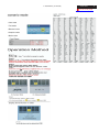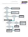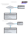
1
ACER
ACER_LCD_G24_SM080519V1
Service
Model ID:MB243WABNS
Service Manual
Table of Contents
Important Safety Notice------------------------------------------------------------------------------------- 01
01. Product Specification--------------------------------------------------------------------------------- 02
02. OSD Menu-----------------------------------------------------------------------------------------------08
03. Exploded Diagram ------------------------------------------------------------------------------------- 10
04. Assembly and Disassembly Procedures-----------------------------------------------------------12
05. Troubleshooting----------------------------------------------------------------------------------------20
06. Firmware Upgrade Procedure------------------------------------------------------------------------31
07. Writing EDID Procedure-------------------------------------------------------------------------------33
08. Schematics and Layouts------------------------------------------------------------------------------ 35
Appendix I : User ’ s Manual
Appendix II: Quick Setup Guide
Appendix II : Spare Parts List
Appendix IV: Software Pack
Safety Notice
Any person attempting to service this chassis must familarize with the chassis and be aware of the
necessary safety precautions to be used when serving electronic equipment
containing high voltage.
Published by LITE-ON Service Printed in Taiwan © All rights reserved Subject to modification
19th-May-2008
Important Safety Notice
ACER G24
Go to cover page
Product Anouncement:
This product is certificated to meet RoHS Directive and
! Using Lead-Free solder to well mounted the parts.
Lead-Free produced definition. Using approved critical
! The fusion point of Lead-Free solder requested in the
components only is recommended when the situation
to replace defective parts. Vender assumes no liability
express or implied, arising out of any unauthorized
modification of design or replacing non-RoHS parts.
Service providers assume all liability.
Qualified Repairability:
Proper service and repair is important to the safe,
reliable operation of all series products. The service
providers recommended by vender should being
aware of notices listed in this service manual in order
to minimize the risk of personal injury when perform
service procedures. Furtermore, the possibile existed
improper repairing method may damage equipment or
products. It is recommended that service engineers
should have repairing knowledge, experience, as well
as appropriate product training per new model before
performing the service procedures.
NOTICE:
! To avoid electrical shocks, the products should be
connect to an authorized power cord, and turn off the
master power switch each time before removing the
AC power cord.
! To prevent the product away from water or explosed
in extremely high humility environment.
! To ensure the continued reliability of this product,
use only original manufacturer s specified parts.
! To ensure following safty repairing behavior, put the
replaced part on the components side of PWBA, not
solder side.
! To ensure using a proper screwdriver, follow the
torque and force listed in assembly and disassembly
procedures to screw and unscrew screws.
degree of 220 ° C.
1
2
ACER G24
1. Product Specification
Go to cover page
1.1 SCOPE
This document defines the design and performance
requirements for a 24W inch diagonal , flat panel monitor
MONITOR SPECIFICATIONS
.The display element shall be a WUXGA (1920x1200)
ITEM
resolution TFT-LCD (Thin Film Transistor Liquid Crystal
Signal Input
Display).16.7M color(RGB Hi+FRC) images are displayed
(Analog)
Frequency
SPEC
Analog :
H : 30kHz~94kHz
V : 55Hz~76Hz
on the panel.Video input signals are analog RGB (0.7Vp-p).
Pixel clock
205MHz (Max)
parameters for a pre-defined mode will be recalled if the
Video Input
Analog
operating mode is one of stored in memory( 24 factory , 9
Display Pixels
640 x 480 (VGA) ~ 1920 x 1200 (WUXGA)
When the systemis powered-on , previously stored screen
users timing ).This monitor operates normal by non-
Signal Input
interlaced mode. DDC (Display Data Channel) function is
(Digital)
Sync Signal
Separate SYNC for TTL (N or P)
Frequency
Digital :
H : 30kHz~94kHz
Pixel clock
165MHz (Max)
V : 55Hz~76Hz
DDC2Bi compliance Power saving function complies with
Video Input
the DPMS (Display Power Management Signaling)
Connector
1.2 GENERAL REQUIREMENTS
LTM240CT03
CA110 or BM7 or same equipment .
Display Pixels
640 x 480 (VGA) ~ 1920 x 1200 (WUXGA)
AC Input
AC100V ~ AC240V ± 10% 50/60Hz , 3 pin AC power cord
Input connector
D-SUB 15 pin & DVI-D
Power Consumption
AC in 100V~240V
active 90W, power saving < 2W
User's Control
Front
Empowering,Auto Adjust,Adjust(-),Adjust (+),Menu,Power
OSD
Contrast , Brightness , Position ,Clock ,Phase
,Analog/Digital,RESET, Color , Language select , etc.
Factory
24
Pre-Defined Timing
pattern test mode following spec. Warm up more than
1 hr, ambient light < 10 Lux , Luminance meter
0.7Vp-p
Audio Jack (OPTIONAL) Audio input 3.6F
1.2.1 Test Condition
Brightness level & contrast level max. Full white
Analog
Input Impedance 75Ω
standard.
AMLCD: LTM240CT01
0.7Vp-p
User
Plug and Play
9
VESA DDC2Bi
Power Saving
VESA DPMS
Input Signal Counter Tolerance
≦ H ± 1kHz, ≦ V ± 1 Hz
1.2.2 Test Equipment
The reference signal source is a calibrated Chroma
2135 video generator or higher.The use of other
signal generators during qualification and production
is acceptable provided the product complies with this
specification.
1.3.1 Interface Connectors
1.3.1.1 Power Connector and Cables
The AC input shall have an IEC/CEE-22 type male
1.3 ELECTRICAL
power receptacle for connection to mains power.
This section describes the electrical requirement of the
The power cord shall be with length of 1.8+/-0.005
monitor. The LCD monitor consists of an interface board , a
meters.
power board , a function key board. The interface board
1.3.1.2 Video Signal Connectors and Cable
wil l house the flat panel control logic , brightness
The signal cable shall be 1.8 +/-0.005 meters long.
control logic, audio function control (option), key function
At the end of the cable shall be a molded-over,
control, DDC and DC to DC conversion to supply the
shielded,triple row, 15 position, D-subminiature
appropriate power to the whole board and LCD flat panel ,
connector. The CPU connection shall have captive
and transmitting LVDS signals into LCD flat panel module
screw locks, which will be adequate for hand
to drive the LCD display circuit .The power board will
tightening. The monitor connection may use small
support main power DC5V to interface board, and the
screws.
power DC5.3V to audio function power of interface board,
and drive the two CCFLs (Cold Cathode Fluorescent
Tube).The interface board provides the power ON / OFF
control over the whole monitor and control for DPMS LED
indicator to function key board.
ACER G24
1. Product Specification (continued)
3
Go to cover page
C o n n ecto r
P in
A s s ig n m e n t
1.3.2.1 Video Signal Amplitudes
D SU B
P in
S ig n a l
P in
S ig n a l
P in
S ig n a l
The three video inputs consist of Red ,Green , and Blue
1
R e d -V id e o
6
R e d -G N D
11
N C
2
G re e n -V id e o
7
G re e n -G N D
12
D D C -S D A
signals, each with its own coaxial cable terminated at the
3
B lu e -V id e o
8
B lu e -G N D
13
H -S Y N C
monitor. These video signals are analog levels, where 0
4
5
N C
D D C -G N D
9
10
+5V
S y n c -G N D
14
15
V -S Y N C
D D C -S C L
V corresponds to black , and 700 mV is the maximum
signal amplitude for the respective color, when each
signal is terminated by a nominal 75.0 ohms .For a given
C o n n e c to r P in D e s c r ip tio n
D -S U B P in D e s c riptio n
P in
N ame
1
R e d - V id e o
2
G re e n- V id e o
3
B lue - V id e o
4
GN D
5
DDC -GN D
6
Red-G N D
7
G re e n- G N D
8
B lue - G N D
9
+5V
10
S ync - G N D
11
GN D
12
DDC _SDA
13
H-SYN C
14
V-SYN C
15
DDC -SC L
monitor luminance levels are measured using this
D e s c riptio n
R e d vid e o signa l inp ut.
G re e n vid e o signa l inp ut.
B lue vid e o signa l inp ut.
G ro und
D D C gro und fo r the V E S A D D C 2 B i func tio n.
A na lo g signa l gro und fo r the R e d vid e o .
A na lo g signa l gro und fo r the G re e n vid e o .
A na lo g signa l gro und fo r the B lue vid e o .
+ 5 V inp ut fro m ho st syste m fo r the V E S A D D C 2 B i func tio n.
S igna l gro und
G ro und
S D A signa l inp ut fo r the V E S A D D C B 2 i func tio n.
H o rizo nta l signa l inp ut fro m the ho st syste m .
V e rtic a l signa l inp ut fro m the ho st syste m .
S C L signa l inp ut fo r the V E S A D D C 2 B i func tio n.
defined video amplitud driving a monitor meeting the
termination requirements .The signal amplitude is not to
be readjusted to compensate for variations in termination
impedance.
1.3.2.2 Video Signal Termination Impedance
This analog video signal termination shall be 75Ω+/-1%
which shall be resistive with a negligible reactive
component .
DVI-I / DVI-D (If using DVI-D cable, C1, C2, C3, C4, C5 is NC)
Pin
1
2
3
4
5
6
7
8
9
10
Signal
RX2RX2+
GND
NC
NC
SCL
SCA
Analog V-Sync (NC)
RX1RX1+
Pin
11
12
13
14
15
16
17
18
19
20
Signal
GND
NC
NC
5V
GND
HP
RX0RX0+
GND
NC
Pin
21
22
23
24
C1
C2
C3
C4
C5
Signal
NC
GND
RXC+
RXCAnalog Red (NC)
Analog Green (NC)
Analog Blue (NC)
Analog H-Sync (NC)
GND
1.3.2.3 Synchronization ( Sync ) Signals
The Horizontal Sync (HS) TTL signal is used to initiate
the display of a horizontal line. HS may be either active
high or active low, depending upon the timing .The
Vertical Sync (VS) TTL signal is used to initiate the
display of a new frame .VS may be either active high or
active low, depending on the timing
1.3.2.4 Sync Signal Levels
The monitor must accept sync signals from both 3.3 and
5 volt TTL logic families.The inputs shall sense a logic 0
DVI-I / DVI-D ConnectorPinDescription
Pin
1
2
3
4
5
6
7
Name
RX2RX2+
GND
NC
NC
SCL
SDA
Description
TMDS link #0 channel#2 differentialpair
TMDS link #0 channel#2 differentialpair
GNDfor no link share
NC
NC
Clock line for DDC interface
Data line for DDC interface
Pin
16
17
18
19
20
21
22
Analog
V-sync for analoginterface
V-Sync
9 RX1- TMDS link #0 channel#1 differentialpair
8
10 RX1+
TMDS link #0 channel#1 differentialpair
11 GND
GNDfor no link share
12 NC
NC
13 NC
NC
14 5V
+5Vinput fromhost systemfor DDC2Bfunction.
15 GND
Ground(Usingas Detect Cable)
Name
HP
RX0RX0+
GND
NC
NC
GND
Description
Hot plugging
TMDS link #0 channel#0 differentialpair
TMDS link #0 channel#0 differentialpair
GNDfor no link share
NC
NC
Clock shield
when the input is 0.8 volt or less and shall sense a logic
23 RXC+
TMDS clock differentialpair
(typically by using a Schmitt Trigger input ).That is , the
24 RXCAnalog
C1
Red
Analog
C2
Green
Analog
C3
Blue
Analog
C4
H-Sync
Analog
C5
GND
TMDS clock differentialpair
input level at which the monitor actually detects a logic 0
1 when the input is 2.0 volts or greater. In addition to
these level requirements, there shall also be a minimum
of 0.3 volt hysteresis provided for noise immunity
AnalogRed signal
shall be at least 0.3 volt lower than the level at which it
AnalogGreensignal
actually detects a logic 1.If the monitor sync processing
AnalogBlue signal
circuits are designed around the 3.3 volt logic family
H-sync for analoginterface
,then the sync inputs must be 5 volt tolerant .
1.3.2.5 Sync Signal Loading
AnalogGND
TTL input loading shall be equivalent to one TTL input
load. When logic 0 is asserted by a sync input , the
maximum current source from any single monitor sync
input to the driver is 1.6 mA .When logic 1 is asserted ,
the maximum current source from the driver to any
single monitor sync input is 400 uA .
1.3.2 Video Input Signals
V id e o
N o .
S y m
b o l
F h
S c a n n in g
2
3
F v
V ih
S c a n n in g
V e r tic a l
H i L e v e l I n p u t
4
V il
L o w
5
V id e o
N o te
1 )
I n p u t
I t e m
1
R G B
L e v e l
F re q u e n c y
F r e q u e n c y
I n p u t
A n a lo g
S c h m itt- T rig g e rs
S ig n a l
M
H o riz o n ta l
V id e o
L e v e l
I n p u t , S u p p o r te d
3 .3 V
in
N o r m a l
M
a x
U n it
R e m a r k
3 0
9 4
k H z
M
in im u m
r a n g e
5 5
2
7 6
5
H z
M in im u m
N o te
1 )
r a n g e
0
0 .8
V
N o te
V
7 5 Ω
0 .0
0 .7
d e v ic e
H (& V )
1 .0
s y n c
o u tp u t fr o m
P C .
1 )
to
G ro u n d
ACER G24
4
1. Product Specification (continued)
Go to cover page
1.3.3.4 OSD adjustment
1.3.2.6 Abnormal Signal Immunity
The monitor shall not be damaged by improper sync
timing , pulse duration , or absence of sync , or
ITEM
CONTENT
abnormal input signal amplitude ( video and/ or sync
BRIGHTNESS
Back light Luminance of the LCD panel is adjusted.
too large or too small) , or any other anomalous
CONTRAST
A gain of R , G and B signal is adjusted.
behavior of a graphics card video generator when
AUTO CONTRAST
A gain of R , G and B signal auto adjust.
changing modes , or when any combination of input
CLOCK
The ratio of dividing frequency of the dot clock is adjusted.
signals is removed or replaced . Additionally , under
PHASE
The phase of the dot clock is adjusted.
these conditions , the monitor shall not cause
H-POSITION
The indication screen is horizontally moved right and left (1 Pixels pitch).
damage to the driving source
V-POSITION
The indication screen is vertically moved up and down (1 Pixels pitch).
AUTO ADJUST
Clock system auto adjustment, about under 8 sec.
COLOR BALANCE
Select three kinds of modes. ( USER /WARM / Cold ).
1.3.3 User Controls and Indicators
1.3.3.1Power On / Off Switch
The monitor shall have a power control switch
visible and accessible on the front of the monitor .
OSD POSITION
The OSD indication position can be adjusted.
OSD LANGUAGE
Select the language used for the OSD menu among English , French ,
Italian , Deutsch and Spanish.
The switch shall be marked with icons per IEC 417 ,
RECALL DEFAULTS All data copy from factory shipment data.
# 5007 and # 5009.The switch shall interrupt the DC
OSD DURATION
Adjust OSD menu off time range from10~120 second.
POWER-SAVE
Back light of the LCD panel is cut when the signal is not input (AC line
power consumption 2W or less).
INFORMATION
The frequency of the horizontal / vertical synchronizing signal under the
input is indicated.
supply to the monitor
1.3.3.2 Power Indicator LED
The monitor shall make use of an LED type
indicator located on the front of the monitor .
※ NOTE : OSD MENU SEE APPENDIX A
The LED color shall indicate the power states as
given in Table 1.
1.3.4 Monitor Modes and Timing Capability
1.3.4.1 Format and Timing
Table 1
Function
LED Color
Full Power
Blue color
Sleep
Orange color
The monitor shall synchronize with any vertical
frequency from 55 to 76 Hz , and with any
horizontal frequency from 30 to 94KHz. If the input
frequency is out of the above – specified range,
the monitor shall display a warning screen
indicating that the input frequency is out of range.
1.3.3.3 On-Screen Display
The Lite-ON On Screen Display system shall be
Under no circumstances shall any combination of
used , controlled by a Menu button. If the buttons
input signals cause any damage to the monitor .
remain untouched for OSD turn off time while
1.3.4.2 Factory Assigned Display Modes
displaying a menu , the firmware shall save the
There are 24 factory pre-set frequency video
current adjustments and exit. Also, if the video
modes. These modes have a factory pre-set for all
controller changes video mode while the OSD is
characteristics affecting front-of-screen
active, the current settings shall be saved
performance. When the system is powered-
immediately, the OSD turn off, and new video mode
on,previously stored screen parameters for a pre-
is displayed.
defined mode will be recalled if the operating
mode is one of those stored in memory. If the
Description
Key
MENU
When no OSD display OSD Displayed
Menu Display
1. To display the OSD menu on the screen.
memory, the monitor CPU will select the PRESET
2. To select the OSD sub-Menu
timing for a mode that is the next lowest in
1. Back-forward selection of the OSD menu.
2. Decrease the value after sub-menu selected.
horizontal scanning frequency to the mode being
>
Speaker Volume/Plus
(with Audio)
<
Speaker Volume/Minus 1. Forward selection of the OSD menu.
(with Audio)
2. Increase the value after sub-menu selected.
Auto
Auto Adjust Function
operating mode is not one of those stored in
Menu or sub.menu auto adjust
currently used. The screen parameters may be
adjusted by the use of the front bezel controls and
then may be saved as a user defined mode. The
E
Empowering
Menu or sub.menu EXIT/Scenario mode
monitor shall include all the preset video timings
shown in the following page.(Please see Note.(3) )
1. Product Specification (continued)
ACER G24
5
Go to cover page
1.3.4.3 Mode Recognition Pull-in
■ Digital inputs (DVI, HDMI): Conflicting video- and PC
The monitor shall recognize preset modes within a
timings are to be treated as Video timings with one
range of +/-1KHz whichever is less for horizontal ;
exception: 640x480p/60Hz timing to be treated as PC-timing.
and within +/-1Hz for vertical.
■ Analog input (VGA) treats all timings as PC-timings.
1.3.4.4 User Display Modes
In addition to the factory pre-set video modes,
provisions shall be made to store up to 9 user
modes. If the current mode is a user mode, the
1.3.5 Controller Requirements
1.3.5.1 General Requirements
The monitor shall include a controller capable of
monitor shall select its previously stored settings.
converting the analog RGB signal from a standard
If the user alters a setting, the new setting will be
WUXGA resolution video controller in the CPU to a
stored in the same user mode. The user modes
signal which can be displayed on the panel. The
are not affected by the pre-set command. If the
controller will include a PLL, A/D converters, LVDS
input signal requires a new user mode, storage of
transmitter and other circuitry necessary to perform
the new format is automatically performed during
its function. The PLL shall be stable enough to
user adjustment of the display (if required).(
ensure that a static image from the CPU is placed
Please see Note.(4) )
in the same physical location on the flat panel in
Preset timing Chart
each frame.
P reset T im in g C h a rt
1
2
3
4
7 20
6 40
6 40
6 48
400
480
480
500
H -S y nc
(K H z)
31 .4 72
31 .4 69
3 7.5
31 .2 34
5
6
8 00 x 6 0 0
8 00 x 6 0 0
37 .8 79
46 .8 75
60 .3
75
7
10 2 4 x 76 8
48 .3 63
60
65
-
8
10 2 4 x 76 8
60 .0 23
75
78 .7 5
+
9
1 2 80 x 1 0 24
63 .9 81
60
1 08
+
+
VESA
Item
10
11
12
13
14
15
16
17
18
19
20
21
22
23
24
NOTE :
R eso lu tio n
x
x
x
x
1 2 80 x 1 0 24
V -S y n c B an d W idth
(H z)
(M H z)
70 .4
2 8 .3 25
5 9 .9 4
2 5 .1 75
75
3 1.5
5 7.73 5
3 1 .2 34
79 .9 76
40
4 9.5
75
1 35
P o larity
H
V
+
+
+
+
+
+
+
+
1.3.5.2 Video Stretching
S ou rce
The monitor shall contain provisions to “stretch” the
VGA
VGA
VESA
M AC
video signal, so that an input signal from the
VESA
VESA
computer in any resolution smaller than 1920 x
-
VESA
1200 is automatically expanded to fill the entire
+
VESA
+
screen.
1.3.5.3 Panel Timing and Interface
VESA
14 4 0 x 90 0
55 .4 69
5 9 .0 1
88 .7 5
+
C V T -R B
14 4 0 x 90 0
55 .9 35
5 9.88 7
10 6 .5
+
CVT
14 4 0 x 90 0
70 .6 35
7 4 .9 8
1 3 6.75
+
CVT
12 8 0 x 72 0
45
60
74 .2 5
+
+
C E A -8 61
12 8 0 x 80 0
49 .7 02
60
8 3.5
+
CVT
12 8 0 x 80 0
62 .7 95
75
10 6 .5
+
CVT
1 6 00 x 1 2 00
75
60
1 62
+
+
VESA
1 6 00 x 1 2 00
74 .0 06
5 9.92 4
1 3 0.25
+
C V T -R B
1 6 00 x 1 2 00
93 .7 5
75
20 2 .5
+
+ /VESA
1 6 80 x 1 0 50
65 .2 9
5 9.95 4
1 4 6.25
+
CVT
1 6 80 x 1 0 50
64 .6 74
5 9.88 3
1 19
+
C V T -R B
1 6 80 x 1 0 50
82 .3 06
7 4.89 2
1 87
+
CVT
1 9 20 x 1 2 00
74 .0 38
5 9 .9 5
1 54
+
C V T -R B
1 9 20 x 1 2 00
74 .5 56
5 9.88 5
1 9 3.25
+
CVT
(1 ) 76 ≦ F V ≦ 8 6 : m on ito r can d isp lay bu t do esn't gu aran tee.
(2 ) fV < 5 5, o r fV > 86 : w arn in g in v alid m o de.
(3 ) F acto ry m od el :
A fter w e first b urn th e co de into th e flash , every p reset-m o del w e run first m u st d o au to -adjustin g .
T h en it'll n ot d o au to -adjust again w h en w e chan ged p reset-m o de b ack in clu d in g A C o n /o ff D C on /o ff.
T h e on ly w ay th at preset-m o d e d o au to -ad ju st ag ain is p ress '' Internal F actory R eset''.
(4 ) U ser m od e :
T h e co de sh ou ld m em orize 9 tim in g m o de ex clusive o f p reset-m od es as u se m o de an d d o au to -adju stin g .
W h en u ser set a n ew m o de th at is no t am on g p reviou sly . It'll do auto-ad ju stin g th en b e so lv ed to u ser m o de
T h e new m o d e w ill ov erw rite the first m em o rized u ser m od es.
T h e user m o des b e cleared is sam e as F acto ry m od e. Ju st do '' In ternal F acto ry R eset''.
(5 ) Internal F acto ry R eset an d O S D F acto ry R eset behavior.
FACTORY PRESET VIDEO TIMINGS (DIGITAL INPUTS)
The controller supplied with the monitor shall
control all panel timing. This controller shall
adequately insulate the monitor from the computer,
so that no possible combination of input signals
from the computer shall cause damage to the flat
panel or any other component of the monitor. The
LCD panel interface shall support the TFT
standard.
1.3.6 DC - AC Inverter Requirements
The DC-AC inverter is on the power board. The
frequencies used by the DC-AC inverter used to power the
backlight shall be chosen so as to prevent any noticeable
effects on the flat panel (such as a rolling effect).
Pixel
CEA-861-C
H-Active
V-Active
I/P
H-tot.
HB
V-tot.
H-freq
V-freq
(kHz)
(Hz)
VB
code
freq
Inputs
(MHz)
1.3.7 Power Supply Requirements
The AC to DC converter power supply for the monitor shall
17,18
720
576
P
864
144
625
49
31.250
50.000
27.000
DVI,HDMI
19
1280
720
P
1980
700
750
30
37.500
50.000
74.250
DVI,HDMI
20
1920
1080
I
2640
720
1125
22.5
28.125
50.000
74.250
DVI,HDMI
have an IEC receptacle for main power input and a pin - in
21, 22
1440
576
I
1728
288
625
24.5
15.625
50.000
27.000
HDMI
---socket for DC power out. The brick shall provide
31
1920
1080
P
2640
720
1125
45
56.250
50.000
148.500
DVI,HDMI
sufficient power for both the monitor and the backlight
39
1920
1080
I
2304
384
1250
85
31.250
50.000
72.000
DVI,HDMI
2, 3
720
480
P
858
138
525
45
31.469
59.940
27.000
DVI,HDMI
4
1280
720
P
1650
370
750
30
44.955
59.940
74.176
DVI,HDMI
5
1920
1080
I
2200
280
1125
22.5
33.716
59.940
74.176
DVI,HDMI
6, 7
1440
480
I
1716
276
525
22.5
15.734
59.940
27.000
HDMI
16
1920
1080
P
2200
280
1125
45
67.433
59.940
148.352
DVI,HDMI
be an external AC to DC converter ”brick” This brick shall
assembly, and shall meet requirements specified in Table
2.
ACER G24
6
1. Product Specification (continued)
Go to cover page
Table 2
AC to DC Converter Requirements
1.4.2 Panel Timings
The controller included with the monitor shall translate all
Input Voltage Range
The operating range shall be from 90 to 132 and 195 to 265 AVC
sinusoidal for all models specified.
Input Frequency Range
Input power frequency range sha;; be from 47.5 to 63 Hz over the
specified input voltage range.
Power Consumption
Power consumption for the monitor shall be less than 46W over the
specified voltage and frequency ranges. In suspend or sleep mode
the power consumption will be less than 2W.
Line Fuse
The AC input shall be fused and become electrically open as a result
on an unsafe current level. The fuse many not be user replaceable.
The power supply shall start and function properly when under full
load, with worst case conditions of input voltage, input frequenct,
operating temperature, and cold backlight lamps.
CPU , so that the panel shall always be driven per it's own
Initial Cold Start
CPU.
Inrush Current
The inrush current must be limited to 30A when operated at
120VAC, and 50A when operated at 220VAC. Inrush current is
measured at an ambient temperature of 25oC, with the unit
temperature stabilized in the power-off.
Hot Start Cycle
The power supply shall be damaged when switched ON for one
second and OFF for one second for seven consecutive after
operating for one hour at full load, 25oC, and nominal input line
voltage.
Under Voltage
The power supply shall contain protection circuitry such that the
application of an input voltage below the minimum specified in this
table shall not cause damage to the power supply unit nor cause
failure of the input.
Line Transient
The power supply shall operate within IEC 801-4 (± 1KV) and IEC
801-5 (± 2KV) for the domestic U.S. version. The UPS power
supply shall operate and comply with CE mark.
1.3.8 Display Communications Channel
The monitor assembly shall provide a display
communications channel that conforms to VESA
DDC2Bi hardware requirements. This configuration
shall contain the 128-byte EDID file as specified by
VESA EDID standard.The monitor should not write to
the EDID file for the first two minutes of operation
following power-up UNLESS some action taken by the
user or the host CPU forces the write (for instance,
requesting the serial number via the OSD).
Furthermore, it is recommended that CMOS switches
be incorporated to isolate the DDC IC from outside
connections while the EDID Fault Management is
being updated. This is to prevent corruption of the data
by attempts to read the data while it is being changed.
1.3.9 Firmware Update Function (same ISP function)
The update firmware need through from the D-Sub
connector, use DDC I2C bus to do update firmware.
1.4 PANEL ELECTRICAL
1.4.1 General Requirements
The panel used as the display device shall be an
WUXGA resolution, 24W TFT-LCD. This panel shall be
approved for use in this monitor.
video timings from the CPU that meet the timing
requirements listed in Panel specification into timings
appropriate for the panel. Under no circumstances may the
controller supply the panel with timings that may result in
damage. The controller shall insulate the panel from the
specification regardless of the timings being sent from the
1.4.3 Polarizer Hardness
The outer face of the front polarizer panel shall be
covered with a coating with a # 3 hardness value .
1.4.4 Backlight Requirements
1.4.4.1 General Requirements
The backlight assembly shall be designed to
support field replacement at the customer site or
authorized service center. The lamps shall have a
continuous operating life of at least 40,000 hours at
25. The operating life is defined as having ended
when the illumination of light has reached 50% of
the initial value. The lamps shall extend a sufficient
amount from the edge of the light guide that
sputtering over the life of the lamps shall not cause
degradation of the luminance uniformity (such as
non-illuminated bands along the edges of the
display).
1.4.4.2 Lamps Startup Time
The backlight lamps shall start about 2 sec of the
time the monitor power switch is pressed or the
monitor is restarted from a power - down mode
.The starting time shall stay about 2 sec. for the
minimum expected life of the lamps.
Test conditions are as follows :
Ambient Light ----------------------
< 1.0 lux
Temperature--------------------------
10℃
Inactive Time -----------------------
> 24 hours
1.4.5 Defects
1.4.5.1 Visual Inspection
The LCD panel shall be inspected with all pixels
set to white,black , red , green , and blue. The color
variation, brightness variation , and overall
appearance must not be perceived as poor quality
by Lite-On . Areas and / or parameters considered
questionable shall be subjected to detailed
measurements .
ACER G24
1. Product Specification (continued)
7
Go to cover page
1.4.5.2 Display Degradation
Over the life of the product , variation of the parameters
1.4.5.6 Smudges, Streaks and Smears
specified in Panel specification shall be maintained
When viewing the panel oriented so as to maximize
within reasonable limits.The panel must not exhibit any
reflected light , there shall be no visible smudging ,
significant defects while in operation ( excluding the
streaking, smearing or other nonuniformity from
CCFL operation ).This does not in any way change the
contaminants ,fingerprints,or defects in any of the
warranty given by the panel manufacturer .
visible surfaces. This is independent of whether the
1.4.5.3 Light Leakage
unit is operating or off .
Except for the active display area , there shall be no
1.4.5.7 Other Defects
light emission visible from any angle from any other part
Undefined defects that are considered to be
of the display . For this test , the ambient illumination
rejectable by Lite–On will be reviewed by Lite-On as
must follow panel's specification.
they become apparent. These panels will be referred
1.4.5.4 Allowable Defects
No cosmetic defects are allowed except those specified
below.The conditions of visual inspections are as follows
to the Lite - On Corporate / Manufacturer Purchasing
Agreement for disposition.
1.4.5.8 LCD Inspection
For 24W Series.
Put LCD panel on inspection table and illuminate the
■Viewing distance is to be approximately 35-50cm
panel with a daylight fluorescent lamp located above
■Ambient illumination is to be 300 to 700 lux.
the panel surface such that the luminance at the
■Viewing angle shall be at 90 degree.
LCD panel is between 1000 lux and 1500 lux .Defect
limits are given in Table 4 .
■Defects not apparent within one minute shall be
ignored.
1.4.5.5 Defect Terminology
Table 3 gives the descriptive terms used in classifying
defects.
D a rk / S p o ts / L in e s
S p o ts o r lin e s th a t a p p e a r d a rk in th e d is p la y p a tte rn s a n d a re
u s u a lly th e re s u lt o f c o n ta m in a tio n . D e fe c ts d o n o t v a ry in
s iz e o r in te n s ity (c o n tra s t) w h e n c o n tra s t v o lta g e is v a rie d .
C o n tra s t v a ria tio n c a n b e a c h ie v e d th ro u g h th e u s e o f v a ry in g
g ra y s h a d e p a tte rn s .
B rig h t S p o ts / L in e s
S p o ts o r lin e s th a t a p p e a r lig h t in th e d is p la y p a tte rn s .
D e fe c ts d o n o t v a ry in s iz e o r in te n s ity (c o n tra s t) w h e n
c o n tra s t v o lta g e is v a rie d . C o n tra s t v a ria tio n c a n b e a c h ie v e d
th ro u g h th e u s e o f v a ry in g g ra y s h a d e p a tte rn s .
P o la riz e r S c ra tc h
W h e n th e u n it lig h ts , lin e s a p p e a r lig h t (w h ite ) w ith d is p la y
p a tte rn s d a rk a n d d o n o t v a ry in s iz e . P h y s ic a l d a m a g e to th e
p o la riz e r th a t d o e s n o t d a m a g e th e g la s s
P o la riz e r D e n t
W h e n th e u n it lig h ts , s p o ts a p p e a r lig h t (w h ite ) w ith d is p la y
p a tte rn s d a rk a n d d o n o t v a ry in s iz e . P h y s ic a l d a m a g e to th e
p o la riz e r th a t d o e s n o t d a m a g e th e g la s s .
R u b b in g L in e
N e w to n R in g
M o ttlin g
D im L in e
H o riz o n ta l o r d ia g o n a l lin e s th a t a p p e a r g ra y w ith th e d is p la y
p a tte rn s d a rk a n d m a y h a v e re s u lte d fro m a n “ o u t o f c o n tro l”
ru b b in g p ro c e s s o n th e p o ly im id e o r “ w a v e s ” o n th e B E F s o r
p ris m s h e e ts .
T h e “ ra in b o w ” e ffe c t c a u s e d b y n o n -u n ifo rm c e ll th ic k n e s s .
W h e n th e u n it lig h ts , v a ria tio n / n o n – u n ifo rm ity
(s p lo tc h in e s s ) a p p e a rs lig h t (w h ite ) w ith th e d is p la y a n d
m ig h t v a ry in s iz e .
W h e n th e u n it lig h ts , lin e (s ) in th e m o n ito r (v e rtic a l) o r m a jo r
(h o riz o n ta l) a x is a p p e a r d im , b u t n o t c o m p le te ly o n o r o ff.
C ro s s L in e s O ff
W h e n th e u n it lig h ts , lin e s in b o th th e m in o r a n d m a jo r a x is
d o n o t a p p e a r.
B rig h t / D a rk D o t
A s u b – p ix e l (R ,G ,B d o t) s tu c k o ff / o n (e le c tric a l).
Average Diameter smaller of
(L+W)/2 or L/20+2W
Acceptable Number
Minimum Separation
< 0.1mm
Non countable
N/A
0.1 mm ~ 0.3 mm
10
15 mm
0.31 mm ~ 0.5 mm
10
15 mm
0.51 mm ~ 1.25 mm
5
15 mm
1.26 mm ~ 2.5 mm
3
25.4 mm
2.51 mm ~ 3.75 mm
3
25.4 mm
Greater than 3.75 mm
NONE
Not applicable
Note : Allowable distance between spots of two sizes is the minimum separation
number for the smaller spot. Therefore, if there are two spots, 1.30mm and 0.4mm
in diameter, they must be at least 15mm apart.
1.5 Optical Characteristics
Depends on the LCD supplier's spec. Details refer to QA
Inspection Spec.
8
ACER G24
Go to cover page
2.1 MAIN OSD MENU
Outline:
The description for control function:
2 OSD Menu
2. OSD Manu (continued)
ACER G24
Go to cover page
9
10
ACER G24
Go to cover page
3.1 Packing Exploded Diagram
3. Exploded Diagram
3. Exploded Diagram (continued)
ACER G24
Go to cover page
3.2 Product Exploded Diagram
11
ACER G24
12
4. Assembly and Disassembly Procedures
Go to cover page
4.1 Assembly procedures:
Connect the cable between power board(P802)
S1
and interface board (P301)
Use a Phillips-head screwdriver screwed the
S4
No.1~4 screws till that interface board and bracket
Connect the function key cable into interface
chassis base firmly attached.
board(P303)
(No1~4 screw size=M3x6; Torque=9~10KGFxCM).
Connect the cable between power board(P803)and
2
3
inverter board (Cn001)
Connect the FFC cable into interface board
P301
1
4
P802
CN01
P803
P303
S5
Take a bracket chassis base on a protective
S2
Take the key function cable out from the hole
shown as photo
Fix the function key cable with a PVC tape
cushion and stick an insulator on the specific
position, take a power board and turn it over. Then,
put it on the specific positions of bracket chassis
base.
No.1~5 screws till that power board and bracket
Turn over the bracket chassis base then fix the
inverter board
Use a Phillips-head screwdriver screwed the
No.1~4 screws till that inverter board and bracket
chassis base firmly attached.
chassis base firmly attached.(No1~4 screw
(No1~4 screw size=M3x6; Torque=9~10KGFxCM).
S6
Use a Phillips-head screwdriver screwed the
S3
size=M3x6; No5 screw size=M4x8;
Torque=9~10KGFxCM).
4
2
1
1
2
3
3
5
4
4. Assembly and Disassembly Procedures (continued)
ACER G24
13
Go to cover page
S7
Connect cable into inverter board(CN001)
Take an inverter shielding bracket to cover the
inverter board
Use a Phillips-head screwdriver screwed the
No.1~6 screws till that inverter shielding bracket
and bracket chassis base firmly attached.
(No1~6 screw size=M3x4; Torque=9~10KGFxCM).
Plug in parallel direction
1
4
CNOO1
5
2
3
6
Angel < 5 degrees
Connect the FFC cable to the connector of the LCD
S8
panel.
Take lamp cables out from the holes shown as the
S10
photo.
Turn the monitor faced down and put it on the
S9
bracket chassis module till both parts firmly
Connect FFC cable to LCD panel. There are
two locks over here when plugging in should be
noticed
Plug 6 lamp cables to the connectors of inverter
S11
board.
ACER G24
14
4. Assembly and Disassembly Procedures (continued)
Go to cover page
S12
Use a Phillips-head screwdriver screwed the
No.1~4 screws on both side and assemble the
Take a key function board to hook with front
S16
bezeland connect to key function cable.
LCD panel and bracket chassis module.
(No1~4 screw size=M3x6;
Torque=2.5
KGFxCM).
2
1
4
3
S13
Use a Phillips-head screwdriver screwed the
No.1~2 screws. (No1~2 screw size=M4x10;
Torque=5~7KGFxCM).
Put a rear cover on the assembled unit and
S17
press on force mechanisms locked and firmly
attached.
1
2
4
4
3
3
2
2
Use a Hex-head and Phillips-head screwdriver
S14
screwed the DVI , D-SUB and HDMI connectors
1
1
(No.1~4 Hex Nut screws
Size=M3x8;Torque=6.5±0.5KGFxCM).
(No.5 screw size=M3x8;
Torque=6.5±0.5KGFxCM).
Assemble the stand upper side to the rear cover
S18
1
2
5
3
4
through the way of screwing 4 screws till both
units firmly attached.
(No1~4 Screw Size=M4x10; Torque=13
1 KGFxCM).
Use a Phillips-head screwdriver screwed the
S15
No.1~2 screws. (No1~2 screw size=M3x6;
Torque=5~7KGFxCM).
1
2
1
3
2
4
ACER G24
4. Assembly and Disassembly Procedures (continued)
15
Go to cover page
Assemble the hinge cover into both two sides
S19
S23
Take two cushion foams; one is held the above
side of LCD monitor, and another is held the
below side.
S20
Stick a screen card on the front bezel with two
tapes.
Put accessories of stand, DVI cable, and
S24
user’s manual ,power cable on specific
positions as photo below.
PUT CABLE IN THIS POSITION
S21
Stick Vista and TC003 label on the correct
position the same as below photo
PUT USER S
MANUAL IN THIS
POSITION
Move previous assembled parts into the carton then
S25
stick Vista and feature label on the carton then
packing the carton
Take a LDPE+EPE bag to cover the LCD
S22
monitor.
FEATURE LABEL
VISTA LABEL
ACER G24
16
4. Assembly and Disassembly Procedures (continued)
Go to cover page
4.2 Disassembly procedures
S1
Open the carton with a proper tool.
S4
Put returned unit on a protective cushion,then
remove LDPE+EPE bag.
Tear off tapes to remove the screen protector
card then turn over the LCD monitor (screen
faced down),
FEATURE LABEL
VISTA LABEL
S2
Take out all accessories including D-SUB cable
power cable, DVI cables, user’s manual, and
packing material from the carton.
(Note: It depends on whether users returning
the accessories.)
PUT CABLE IN THIS POSITION
S5
Disassemble the stand cover.
PUT USER S
MANUAL IN THIS
POSITION
S3
Take off two cushion foams
S6
Use a Phillips-head screwdriver unscrew 4 screws
to release the stand base.
(No1~4 Screw Size=M4x10;
Torque=13±1KGFxCM).
2
1
3
S7
4
Turn over the LCD monitor (screen faced up).
4. Assembly and Disassembly Procedures (continued)
ACER G24
17
Go to cover page
S8
Put the dissembled monitor closed to by myself
S9
RIGHT SIDE
Hold the one upside corner of the front bezel after
separating the upside of the front bezel
Using properly force to pull up front bezel that will
let the locking mechanism of left side, right side
and down side separated
DOWN SIDE
UP SIDE
LEFT SIDE
Wedge your finger between the front bezel and
the panel, then pry up on the front bezel to
disengage the locking mechanism.
Hold one side of down side that had been
separated from front bezel
Use properly force to pull up front bezel
S10
Insert steel rule between panel and front bezel
.Using properly force to let the locking
mechanism of front bezel and rear cover
separated
Separating all of the locking mechanism of the
front bezel in turn
S11
Unhook the key function board from front bezel,
disconnect the key function cable
ACER G24
18
4. Assembly and Disassembly Procedures (continued)
Go to cover page
S12
Use a Hex-head screwdriver unscrewed 5 screws to
release the DVI ,D-SUB and HDMI connectors
S15
Unplug 6 lamp cables
(No1~4Hex Nut screws
Size=M3x8;Torque=6.5 0.5KGFxCM).
(No.5 screw size=M3x8; Torque=6.5 0.5KGFxCM).
1
2
5
4
3
S16
Disconnect the FFC cable to the connector of
panel.
Use finger to push the lock according to arrow
direction then take out the FFC cable
Use a Phillips-head screwdriver unscrewed the
S13
No.1~2 screws to lease power plug
(No1~2 screw size=M3x10; Torque=5~7KGFxCM).
1
S14
2
Use a Phillips-head screwdriver unscrewed the
No.1~4 screws to disassemble the LCD panel
Take out lamp cables right through the No.1-3
and bracket chassis module.
S17
(No1~4 screw size=M3x6;
Torque=2.5
1
square holes and separate the bracket chassis
module and LCD panel apart.
KGFxCM).
2
1
2
3
3
4
19
ACER G24
4. Assembly and Disassembly Procedures (continued)
Go to cover page
S18
Use a Phillips-head screwdriver unscrewed the
Examine the panel surface accoring to inspection
S21
criteria. Put it aside.
No.1~4 screws to release the interface board.
(No1~4 screw size=M3x6; Torque=9~10KGFxCM).
2
3
1
4
S19
Disconnect the cable from inverter board
Use a Phillips-head screwdriver unscrewed the
No.1~8 screws
(No1~6 screw size=M3x4; Torque=9~10KGFxCM).
(No7~8 screw size=M3x6; Torque=5~7KGFxCM).
Use a Phillips-head screwdriver unscrewed the
S22
Remove inverter shielding bracket
No.1~5 screws to disassemble the power board.
(No 1~4 screw size=M3x6; No 5 screw
size=M4x8; Torque=9~10KGFxCM).
4
8
7
1
3
2
6
5
1
2
4
5
3
S20
Use a Phillips-head screwdriver unscrewed the
No.1~4 screws
(No1~4 screw size=M3x6; Torque=9~10KGFxCM).
Disconnect all of the cable
S23
Remove the inverter board
2
3
P301
1
4
P802
CN01
P303
P803
20
ACER G24
5. Troubleshooting
Go to cover page
5.1 No display on the screen (Screen is black and colour of LED is amber.)
Does OSM display upon pressing
the “MENU” button?
NG
Proceed to “5.5 Abnormal OSM display” section.
OK
Check if the sync signal output
from connected computer and the
video cable is connected properly
OK
Proceed to “5.4 Abnormal Screen” section.
NG
Input the sync signal of computer, or change to a
standard shipped cable for cross test.
ACER G24
5. Troubleshooting (continued)
Go to cover page
5.2 Nothing displays on the screen (Screen is black and colour of LED is blue.)
Check if the backlight is
slightly lightened from upper
corners (right/left) of LCD
panel
Proceed to “5.3 Checking the backlight unit” section
NG
OK
Does RGB video
signals output
from connected PC host?
NG
1. Change pattern of video signal outputs from
the PC host to optimum resolution.
2. Reconnect the video cable.
3. Cross-test the other workable video cable.
OK
Failure Point
Check if OSM menu
is displayed upon pressing the
“MENU” key
NG
Check if video signal cable
is connected properly between
LCD monitor and PC host
NG
The cable is disconnected.
OK
Proceed to “5.4 Abnormal Screen” section.
OK
Check if 3.3V is
supplied from I301 pin2; 2.5V is
supplied from I303, pin2, and
the 1.8V power is supplied from
I302 pin2.
Failure Point
NG
OK
Check if the
Voltage on I301, I303,
I320 pin3 is high DC
level at 5V.
OK
Failure Point
I301, I302, I303, or I320 is
damaged.
Check all LVDS signal pins;
output from I314
OK
NG
Failure Point
Failure Point
1. The cable is broke between
P306 and LCD panel.
2. LCD panel is defected.
Printed wire is broke or short
between P306, I314
NG
1. Printed wire is broken between
P301 pin1, pin2, pin3, pin4 and
I301, I303, I320.
2. Check power board
21
22
ACER G24
5. Troubleshooting (continued)
Go to cover page
5.3 Check the backlight unit
Check the BKLT_EN signal of
rectangle input P301 pin11 at TTL
high level.
OK
Failure Point
NG
Does the I306 pin16
output a TTLvoltage level
at “H” status? <or> Is BKLT_EN
signal of the rectangle being
output?
OK
Failure Point
Check the PWM signal
supplied from I314
pin251 is a PWM,
pulse-width modulation.
OK
Failure Point
Inverter of LCD module is defected.
NG
1. Printed wire is broke
between I314 pin251 and P301.
2. I314 is defected.
NG
Printed wire is broken
between I306 pin16 and
P301.
ACER G24
5. Troubleshooting (continued)
Go to cover page
5.4 Abnormal Screen:
Failure Point
Check R.G.B video signals
output from PC host
to D-Sub R.G.B connector
NG
1. Check connected PC host if there’s no R.G.B
signals output.
2. Video signal cable disconnected.
OK
Failure Point
Check the R.G.B signals
on I314 pin40, pin42, and pin45 which
should have voltage level at 0.7Vpp
max.
NG
Green, Blue, Red signals are flow in the same
path. In the case, the Red signal is example.
1. Printed wire is broken between D-Sub [R] and
I314 pin45.
2. R391 is short.
3. C356 is open.
4. R390 is open.
OK
Failure Point
Check all LVDS signal pins
of I314 whether if
output correct signals.
OK
Proceed to “5.8 Checking the resolution change
IC movement” section.
NG
1. The I314 is defected.
2. Printed wire is broken between I314 and P306.
23
24
ACER G24
5. Troubleshooting (continued)
Go to cover page
5.5 Abnormal OSM display - OSD Adjusment Problem
Failure Point
Check the input TTL level
whether if it was altered upon
pressing the function keys.
OK
Proceed to “5.4 Abnormal Section”
NG
1.
2.
3.
4.
5.
6.
7.
8.
Printed wire is broken between P303 pin 2 and I306 pin 87.
Printed wire is broken between P303 pin 3 and I306 pin 88.
Printed wire is broken between P303 pin 4 and I306 pin 89.
Printed wire is broken between P303 pin 5 and I306 pin 90.
Printed wire is broken between P303 pin 6 and I306 pin 22.
Printed wire is broken between P303 pin 7 and I306 pin 1.
C325, C326, C327, C328, C329,C330 is short.
R339, R340, R341, R342, R343, R346, R347, R348,
R349, R350 ,R351, R352 is short or open.
9. I306 is defected.
(Note: more than one components defected is possible.)
ACER G24
5. Troubleshooting (continued)
Go to cover page
5.6 Abnormal Plug and Play Operation
5.6.1 Abnormal DDC2 (D-SUB)
Failure Point
Confirm the output of serial
data on I312 pin6 synchronize SCLK at
TTL level
NG
I312 is defected
OK
Failure Point
1. The host machine isn’t communicating in DDC2 mode.
2. The video cable may have defected or may not be established
connection for DDC.
3. The I312 pin6 and P304 pin15 may have no signal or incorrect.
4. The R374, R377 is open.
5. I312 pin6 is short.
6. The input source cable is defected.
7. Check I312 pin5 signal whether if correct.
5.6.2 Abnormal DDC2 (DVI)
Failure Point
Confirm the output of serial
data on I313 pin6 synchronize SCLK at
TTL level
NG
OK
Failure Point
1. The host machine isn’t communicating in DDC2 mode.
2. The video cable may have defected or may not be established
connection for DDC.
3. The I313 pin6 and P305 pin6 may have no signal or incorrect.
4. The R393 or R397 is open.
5. I313 pin6 is short.
6. The input source cable is defected.
7. Check I313 pin5 signal whether if correct.
I313 is defected
25
26
ACER G24
5. Troubleshooting (continued)
Go to cover page
5.7 Checking the interface circuit of sync signal
5.7.1 Checking the control circuit of horizontal sync pulse
Failure Point
Check the horizontal
sync signal on I314 pin46
TTL level
NG
1.
2.
3.
4.
5.
Video cable is defected.
Printed wire is broken between P304 pin13 and I314 pin46.
FB305, R364, R363 is open.
R371, C336, D305 is short.
I311 is defected.
OK
Proceed to “5.8 Checking the
resolution change IC movement”
section
5.7.2 Checking the control circuit of vertical sync pulse
Failure Point
Check the vertical sync
signal on I314 pin47 TTL level
OK
Proceed to “5.8 Checking the resolution
change IC movement” section
NG
1.
2.
3.
4.
5.
Video cable is defected.
Printed wire is broken between P314 pin14 and I314 pin47.
FB306, R368, R369 is open or more than one component.
R370, C335, D303 is short.
I311 is defected.
ACER G24
5. Troubleshooting (continued)
Go to cover page
5.8 Checking the resolution change IC movement
Is there +3.3V
Supplied on I314 pin107,
pin48, pin61, pin250, pin12, pin70,
pin170, pin184, pin203, pin216,
pin236, pin252, pin20, pin28,
pin38, pin19, pin37,
pin131?
NG
Proceed to “5.9 Checking the DC/DC converter
circuit” section
NG
Proceed to “5.9 Checking the DC/DC converter
circuit” section
OK
Is there +1.8V
supplied on I314 pin16, pin22,
pin50, pin2, pin78, pin96, pin143,
pin160, pin181,
pin225
OK
Is 14.318MHz
clock input to I314 pin35
and pin36 at TTL level
during power on?
NG
Failure Point
Is 14.318MHz clock output
from X302 pin1 at TTL level
during power on?
X302 is defected.
OK
Failure Point
Print wire is broken between X302
pin1 and I314, pin36
Is +3.3V supplied to
I314 pin9 at low level
(Reset again)?
NG
OK
Failure Point
Failure Point
Check the output
of 3.3V “H” pulse from
I306 pin12
I314 is defected.
OK
Failure Point
Print wire is broken between I306
pin12 and I314 pin9.
NG
I306 is defected.
27
28
ACER G24
5. Troubleshooting (continued)
Go to cover page
5.9 Checking the DC/DC converter circuit
Failure Point
Check if the 5V is output
from P301 pin1, pin2, pin3, pin4
to I301, I303, I320 pin3.
NG
Printed wire is broken between
P301 pin1, pin2, pin3, pin4 and
I301, I303, I320 pin3.
OK
Check if the 3.3V, 2.5V
and 1.8V line voltage is output
from I301, I302, I303 pin2
NG
Is the output
FB301 being supplied to
I301, I303, I320 pin3?
OK
NG
OK
Failure Point
Printed wire is broken
between I301, I302, I303
pin2, and I314 power supply
pin.
Failure Point
I301, I303, I320 is defected.
Failure Point
Printed wire is broken
between I301, I303, I320
pin3 and output of FB301
5. Troubleshooting (continued)
ACER G24
Go to cover page
5.10 Checking the inverter board circuit
Does 22V output pin
have voltage around 20V?
Does On/Off pin have voltage over 3V?
Does brightness pin have voltage in
the range of 0V~3.2V?
NG
Check F101, I101, Q110, Q111, Q112,
Q113 and repair them if be damaged
OK
Does I101 pin6 have 5V output?
NG
Check I101 and repair them if be damaged
NG
Check CCFL and repair if damage.
NG
Check I101 and repair if damage
NG
Repair 101
OK
Check D102, D103, D107, D108, D114,
D115, D112, D113 and repair if damage.
NG
Check Q104, Q105, Q106, Q107, Q108 and
repair them if damage
NG
Check T101 and T102 if damage
OK
Does P101, P102, P103,
P104 be firmly connected?
OK
Does I101 pin4, pin5
have triangle pulse?
OK
Does I101 pin1 have soft
start edge up to 2.4V?
OK
Does I101 pin8 have
voltage up to 1.2V from output
detection?
NG
Does
half bridge (Q104,
Q105, Q106, Q107, Q108)
work successful?
OK
Does transformer
(T101, T102) have output AC
voltage to P101, P102, P103,
P104?
OK
Check panel module if damage
29
30
ACER G24
5. Troubleshooting (continued)
Go to cover page
5.11 HDMI signal check
5.11.1 No video
Check the TMDS signal
from computer input on
HDMI connector
Failure Point
NG
1.Check the host PC to see if there’s no TMDS
signal output
2.HDMI cabled disconnected. Reconnect the
cable till firmly connected
3.P311 is disconnected. Reconnect the cable
till firmly connected
OK
Check the TMDS signal of
I322
Failure Point
OK
I322 was damaged.
NG
Failure Point
I314 was damaged
6. Firmware Upgrade Process
ACER G24
31
Go to cover page
Hardware Configuration
Select AUTO DETECT button that will automatically detect
the device then shows “OK” on the right side.
S2. Press [Connect] button.
Connect VGA
cable between
monitor and kit
Connect printer
cable between
PC and kit
Mstar ISP Utility Configuration:
Launch the utility of “ISP_Tool Winbond 0315.exe”
There s a Dialog window shown on the screen. It is the
meaning of connection successful .
Press Config button
Check the video cable and ISP board (D-sub to Printer
port) between LCD monitor to PC host to see if it
disconnected.
ACER G24
32
6. Firmware Upgrade Process (continued)
Go to cover page
Press [Device] button to select the “ WP pin pull to high
Press [Run] button and waiting for firmware upgrade
during ISP “
completed .The screen will show “PASS”
Press [Read] button.
1. Press Read folder to browse firmware image.
2.The position according to where the firmware be put
Check firmware version
Turn off the power,then press force on “ POWER ” and “ E ”
button at the same time then press on “ MENU ”button to
enter factory mode
Note: Please pay attention ,Don’t change any parameter
which is measured by precise machine before shipping out
1
2
Press [Auto] button
When you writing F/W face on interrupting that cause monitor
shut down .
You can unplug AC power then press “AUTO”button and plug
AC power at the same time to solve this problem then re-write
F/W again.
ACER G24
7. Writing EDID Process
33
Go to cover page
1 Writing EDID Procedure
Hardware Configuration:
1.)Connect the PRINTER PLUG of DDC FIXTURE with the
printer port of Desktop PC. (Refer to figure 1)
2.)Plug USB A PLUG of DDC FIXTURE to USB socket of
Desktop PC (Refer to figure 2)
3.)Extend the DVI cable on DVI EXTENDING SOCKET of DDC
FIXTURE. (Refer to figure 3)
4.1)Connect the D-sub plug of Chroma with D-SUB PLUG of
DDC FIXTURE (Refer to figure 4)
4.2) Take a video cable then connect the D-SUB PLUG and the
D-sub socket of monitor. (Refer to figure 5)
5.)Connect the extended DVI cable to DVI socket of monitor
(Refer to figure 5)
6.)Re-confirm all the connectors are connected well.
D-SUB PLUG
DVI EXTENDING
SOCKET
USB A
SOCKET
PRINTER PLUG
4
3.Select Model: Key in password”cedid” then select model
which one you want to write EDID code that it depends on
panel type.
DVI EXTENDING
SOCKET
USB A
PLUG
1
2. Writing VGA/DVI Process
Chose the folder:”Acer-VGA&DVI” then double click
Select the “Acer-M1&M3-XPEDID-DVI-.exe” to execute it
2
5
3
6
CAUTION: The timing of Chroma shall be setup at T254/ P41
before data recording. the detail setting parameter from
chroma .Please See below photo
cedid
34
ACER G24
7. Writing EDID Process (continued)
Go to cover page
4. Choose "WRITE" from menu then select "Scan S/N And
Write EDID And Test DDC”
5. Key in series number(22 characters) in the input column
Press write button after key in S/N
6. When EDID was written successfully that will show below
message on the screen
Writing HDMI Process
Chose the folder:”Acer-HDMI” then double click
Select the “acer HDMI.EXE” to execute it
According to the previous process(step3-step6) to write
HDMI-EDID.
8.Schematics and Layouts
AC
110/220v
Input
Power
Board
Inverter Board
1
2
2
8.1 ACER_LCD_G24_SCHEMATICS_BLOCK DIAGRAM
A
B
C
D
E
F
G
1
3
3
4
DC-DC
5v-3.3v
3.3v-1.8v
Brightness,Inv_On/Off
+5V
P301
I326
I320
I302
I321
Digital
Video
Input
HDMI
DDC
24LC02B
DDC_SCL_D
DDC_SDA_D
4
5
6
LCD Module
LTM240CT03
DVI-D
Switch
7
LVDS
Scaler
8
P306
9
I306
MCU
W79L659A25FL
XTAL
14.3MHZ
I312
9
P304
D_SUB_SCL
D_SUB_SDA
DDC
24LC02B
Analog
Video
Input
DSUB
I314
8
R,G,B,Hs,Vs
MST 9259D
7
P305
I322
TMDS
LTM240CT01
DDC_SCL_D1
DDC_SDA_D1
P311
6
Digital
Video
Input
DDC
24LC02B
I313
EM6A9320BI
DDR
I315
5
10
10
I307
11
Flash
W39L040Ap70Z
11
12
P303
12
PCB No.
13
Function
Key
Board
13
A
B
C
D
E
F
G
ACER G24
Go to cover page
35
P801
L
1
1
3.15AH250V
F801
0.47U/275V
2
C806
0.33U/275V
T802
ET-24
C802
1000P/250V
R0805
R823
61.9K
C813
X7R
C811
1U 1206
3
C817
102P 0805
X7R
R877
R0805
10
R853
C828
680P/250V
VRMS
RI
OTP
IEA
IPFC
1 -
4
D811 1N4007-G
4
C809
L801
280uH
5
CUT
T804
PQ2625
L806
6
BEAD/6mm
Q802
FQPF13N50C
R831
10K
R0805
+
7
VAUX
5.2V
200
R0805
R821
1N4148
2
D806
C804
4700P/1KV
1
8
D801
5
T801
PQ-3225
C805
2200P/250V
FBPWM
1KV X7R
C847
100P
6
3
4
CUT 2
R860
270
R1206
R818
0.33 2W
P6KE180A
D804
LT2A06 -G
Q801
17A/800V
R817
10K
R1206
2
8
C841
0.1 0805
X7R
C826
1U 1206
X7R
C837
1000U/25V
+
VBUS
R869
100K/2W
R868
0.22 1W
R878
680k
R1206
R804
680k
R1206
R805
680k
R1206
1
R806
24K
R1206
R820
10
R0805
R829
100
R0805
L803
2.8U
C836
1000U/25V
R857
4
I807
LTV817
3
VDD
1K
R60A
7
10K
R1206
R859
Q806
KN2907A
Q807
KN2222A
+
VBUS1
C807
103P 1KV
X7R
+ C835
C810
222P 1206
X7R
+ C839
VA
30K
R0805
R858
ZD801
22B
1000U/25V 1000U/25V
6
R854
22K
R60A
R875
100
R60A
R833
15K
R0805
1KV X7R
C801
150U/450V
C848
100P
BEAD/6mm D803
5A/600V
L804
R807
10K
R1206
C858
100P 1KV
X7R
1N4148
R809
10
D805
R0805
1
2
R832
100
R0805
VDD
C819
104P 0805
X7R
D817
X
R872
R1206
R855
20K
R0805
C840
2200P 0805
X7R
D816
FCH30A10
20
D815
R1206
FCH30A10
R873
220P/100V X7R
20
C845
10
R856
4.7K
R0805
I806
AP431 1%
12
2200P/250V
C812
T805
PQ2625
C856
1uF/450V
MEF/P15
R812
604K
R1206
C849
4700P 1KV
X7R
D812 1N4007-G
+
R813
604K
R1206
R830
47K
R0805
R843
220
R0805
C833
47U/50V
VAUX
D809
1N4937-G
3
4
6
CUT 2
C818
103P 0805
X7R
R841
3.3
+
1
1U 1206
X7R
C855
1uF/450V
MEF/P15
11
12
13
14
15
16
17
18
19
20
0.43 2W
0.43 2W
R815
R814
4700P 1KV
X7R
C850
D802
4A/800V
R811
IAC
VEA
OVP
RANGE
OPFC
VDD
ISENSE
SS
OPWM
GND
IPWM
SG6901
R850
0.33 2W
C846 R75A
100P
1KV X7R
VA
L805
D808
PG108R
D807
C843
4700P/1KV P6KE150A
BEAD/6mm
Q803
7N65C
VBUS
AGND
FBPWM
IMP
FBPFC
2.4M
2.4M
R1206
R1206
I801
R810
C829
680P/250V
1
2
3
4
5
6
7
8
9
10
D814
2
2
1N4148
1
100
D810
R0805
1N4148
R849
1
R874
100K/2W
T803
RING CHOKE
C808
1000P/250V
4
100
R0805
R851
10K
R1206
1
R842
1K R0805
+
5
1
R802 C803
510K
R1206
R803
510K
2
R824
24K
R0805
R825
102P 0805
X7R
C814
100P 0805
X7R
10K
R0805
C815 NC
R827
5
6
7
8
2.7KR0805
C816
102P 0805
X7R
I803
GATE
VDD
RT
SENSE
C834
4.7U/50V
+
I804
LTV817
2
C838
4.7U/50V
3
1
3
2
R1206
R826
2.7K
R0805
R828
RI
VIN
FB
GND
100
R1206
R844
510K
R1206
R845
510K
R1206
1
2
3
4
3
C832
470P 0805
X7R
4
3
4
4
5
10
G
N
CON3
SCK055
R801
FBPWM
4
R879
510K
R1206
VBUS1
C830
X7R
102P 0805
2
SG5841J
C831
470P 0805
X7R
3
2
8.2 ACER_LCD_G24_SCHEMATICS_POWER BOARD
A
B
C
R846
100
R0805
C857
0.1U 1206
X7R
R847
33.2K
R0805
1
3
2
3
3
2
2
3
D
E
F
G
1
1
1
12
9
4
3
9
C822
220P 1KV
1
2
10
x
R1206
R876
R839
18.7K 1%
R0805
R838
169K 1%
***
+
+
C824
C823
1000U/35V 1000U/35V
R871 R1206
20
R870
20 R1206
R835
1.2K 0805
10
C821
0.01U 0805
X7R
R822
1K 0805
R836
I805
AP431 1%
4.7K
R0805
X7R
D813
20A/150V
I802
LTV817
C820
1U 1206
X7R
9
L802
2.8U
11
11
+
C825
1000U/35V
12
24V
C827
1U 1206
X7R
12
PCB No.
24V
24V
24V
24V
GND
GND
GND
GND
BRI
ON-OFF
ON-OFF
BRI
5V-RTN
5.2V
5.2V
5.2V
5.2V
5.2V
5.2V
GND
GND
GND
OFF
P803
TO INV
2.0
1
2
3
4
5
6
7
8
9
10
2.0
13
12
11
10
9
8
7
6
5
4
3
2
1
P802
13
13
6832194100P01
A
B
C
D
E
F
G
ACER G24
Go to cover page
36
1
1
2
3
4
5
P301
+5.1V
+5.1V
+5.1V
+5.1V
5V_RTN
6
7
8
9
10
11
12
13
1
3
2
TP1
GND
SOT-223
VOUT
TAB
AIC1117A-33PYTR
ADJ(GND)
VIN
I301
JWT-A2001WV2-13P
GND
GND
GND
AUDIO_DET
AUDIO_EN
BKLT_EN
BKLT_ADJ
OFF
+5V
C312
220u/25V
4
2
TP13
TP17
100u/10V
C313
+3V3
3
8.3 ACER_LCD_G24_SCHEMATICS_INTERFACE_BD_POWER
A
B
C
GND
3 OFF
R570
4.7K
TP549
+5V
10K
R301
Q331
MMBT3904
GND
TP546
R568
4
0
I316
1
2
3
FOR POWER SAVING CONTROL
TP14
5
6
7
+3V3
C306
C307
TP8
C305
TP7
C304
TP5
C302
0.1u
TP4
C301
0.1u
TP470
PBY201209T-170Y-S
5.6K(NC)
100(NC)
100(NC)
100
100
100
FB301
PBY201209T-170Y-S
R302
R303
R304
R305
R306
R496
FB302
C493
0.1u
+5VD
+5VD
0.1u
R308
+5V
8
TP455
TAB
VOUT
SOT-223
VCC_LCD1
VIN
I326
ADJ(GND)
1
3
9
AUDIO_DET
BKLT_ADJ 6
3
1K
+5V
+5V
+3V3
OFF 3
+5VD
GND
GND
11
VIN
I303
+5V
GND
+5V
GND
VOUT
TAB
12
R500
TP456
10K(NC)
R501
47K(NC)
Q313
MMBT3904(NC)
TP458
R502
10K
AUDIO_EN
13
TP457
TP459
BKLT_EN 3
TP23
C315
100u/10V
TP22
6832194600P0
13
100u/10V
C314
+1V8
+2V5_VDDM
R503
47K
Q314
MMBT3904
2
4
2
4
PCB No.
12
TO-252-GOI
ADJ(GND)
TAB
VOUT
AP1117E25L-13
TO-263
I302
VIN
ADJ(GND)
H161R315-8
8
1
AIC1084-18PMTR
M304
1
3
1
3
HI==> POWER ON
TP543
10
R505
10K
100
10K
R504
TP460
R565
TP542
R567
TP545
C538
+3V3D
10uF
M303
100u/10V
C491
TP428
GND
C536
4
2
10uF
Q325
MMBT3904
Q315
MMBT3904
2
4
TO-263
VOUT
TAB
AIC1084-33PMTR
ADJ(GND)
VIN
I320
AIC1117A-33PYTR
GND
1
3
0.1u
C537
+5VD
C535
GND
4.7u
GND
TP16
C311
VCC_LCD2
FB303
C310
PBY201209T-300Y-S
TP15
4.7u
TP544
0.1u
VCC_LCD2
0.1u
5
6
7
8
TP547
3
Q302
AO3401
FDS4435
C309
2
R307
M302
4
5
11
GND
2
M301
1
8
H161R315-8
7
100K
4
5
GND
3
0.1u
1
8
H161R315-8
10
6
0.1u
4
5
GND
2
+3V3
TP18
1
8
H161R315-8
9
7
0.1u
30K
GND
8
3
10K
R309
4
5
7
2
C308
TP19
GND
6
3
7
R488
47K
D301
MM4148
5
6
TP9
TP10
TP11
TP12
6
GND
TP21
47K
Q301
MMBT3904
4
2
220u/25V
TP446
R489
47K
Q309
MMBT3906
TP20
R310
3
1
D
VCC_LCD1
3 LCD_EN
TP445
2
3
7
E
F
G
1
6
4
3
A
B
C
D
E
F
G
ACER G24
Go to cover page
37
8
1
CAM_MIC_DIAG
1
2
I305
STL8110PCH300
OUT
GND
VCC
2
TP54
TP469
R526
10K(NC)
+3V3
GND
Q324
MMBT3904(NC)
R322
4.7K(NC)
0
0
R337
10K
4.7K(NC)
47K(NC)
4
4.7K(NC)
4.7K(NC)
3
+3V3_VDD
R476
R525
4.7K(NC)
4.7K(NC)
4.7K(NC)
4.7K(NC)
4.7K(NC)
4.7K(NC)
8 USB_EN
USB_DET
R468
R469
8
2
RD
WP
TP468
TP70
4.7K
R342
10K
TP76
R336
10K
R335
4.7K
100
0
100
6 INT
6 ALE
2 LCD_EN
BKLT_EN
4 WP_EN
4 DSUB_DET
5 DVI_DET
HP_DET_DVI
6 HWRESET
5
R470
R471
R472
R473
R474
R475
+3V3_VDD
+3V3_VDD
0
RXD
0
R325
TXD R467
R327
R524
0
TP95
TP96
R328
MSCL
MSDA
R338
10K
+3V3_VDD
WE
VGA_SCL_3V
SELECT
R523
VGA_SDA_3V
10u/50V(NC)
C318
+3V3
GND
TP67
WP
R344
R345
6
+3V3_VDD
TP89
R341
10K
10K
R340
10K
R354
TP117
10K
4.7K
TP109
R357
TP540
R360
R361
TP116
E
LED_B
LED_A
RST
ISP
9
10
11
12
13
14
15
16
17
18
19
20
21
22
23
24
25
26
27
28
29
30
2
3
4
5
22p
22p
NC
NC
NC
NC
P5.0
P5.1
P5.2
P5.3
RST
P5.4
P5.5
P5.6
P5.7
P3.0/RXD
P4.3
P3.1/TXD
P3.2/INT0
P3.3/INT1
P3.4T0
P3.5/T1
P3.6/WR
NC
NC
NC
NC
NC
5
R352
10K
TP84
C322
X301
24MHz
C321
TP77
POWER
MSCL
MSDA
GND
R343
10K
Q303
MMBT3906
TP105
Q304
MMBT3906
TP113
5
R346
R347
R348
R349
R350
R351
GND
GND
6
R479
R478
R477
7
+3V3_AVDD
+3V3_VDD
4.7K(NC)
4.7K(NC)
4.7K(NC)
+3V3
8
5
GND
MAD0
MAD1
MAD2
9
C487
TP24
C317
0.1u
+3V3
R331
10K
R332
TP71
10
R512
2
2
+5V
TP429
C488
0.1u
6
11
GND
DVI_SDA
11
VGA_SDA_3V
VGA_SDA
DVI_SDA_3V
TP467
TP58
WR
R321
4.7K
6
+5V
AD[0..3]
+3V3_VDD
GND
FB339
+3V3_AVDD
PBY201209T-300Y-S
10
Q320
2SK3018
R510
X4.7K
+3V3_VDD
4.7K(NC)
R514
Q318
2SK3018
R508
X4.7K
+3V3_VDD
4.7K(NC)
TP500
TP501
TP502
TP503
+3V3_VDD
DVI_SDA_3V
DVI_SCL_3V
VGA_SDA_3V
VGA_SCL_3V
4.7K(NC)
4.7K(NC)
4.7K(NC)
4.7K(NC)
4.7K(NC)
4.7K(NC)
4.7K(NC)
4.7K(NC)
0.1u
R311
R312
R313
R314
R315
R316
R317
R318
0R
0R
0R
0R
MAD3
MAD4
MAD5
MAD6
MAD7
4.7K(NC)
TP57
TP60
R319
R320
R323
R324
MALE
PSEN
TP63
TP65
TP68
R522
A14
A13
A12
10K
+3V3_VDD
R330
TP88
10K
9
TP87
R329
TP86
10
9
8
7
6
5
4
3
2
1
10K
GND
EX
POWER
PLUS
MINUS
MENU
SELECT
TP85
TP78
TP79
TP80
TP83
SDA2
SCL2
SDA1
SCL1
FB304
+3V3_VDD
PBY201209T-300Y-S
I306
W79L659A25FL
80
73
72
71
70
69
68
67
66
65
64
63
62
61
60
59
58
57
79
78
77
76
75
74
A11
A10
A9
A8
AD3
AD2
AD1
AD0
DVI_HDMI_SW
AUDIO_DET 2
AUDIO_EN
2
OFF 2
NC
NC
NC
NC
NC
NC
P0.3/AD3
P0.4/AD4
P0.5/AD5
P0.6/AD6
P0.7/AD7
P6.7/SDA2
P6.6/SCL2
P6.5/SDA1
P6.4/SCL1
EA
/EA
P4.1
ALE
/PSTN
P2.7/A15
P2.6/A14
P2.5/A13
P2.4/A12
+3V3_VDD
TP601
C330
TP94
C329
TP93
C328
TP92
C327
TP91
C326
8
LED_BLUE
LED_AMBER
C325
GND
0.1u
GND
0.1u
GND
0.1u
GND
0.1u
GND
0.1u
GND
7
0.1u
TP90
GND
1K
1K
1K
1K
1K
1K
GND
LED_BLUE
C331
0.1u
LED_AMBER
C332
0.1u
6
MALE
MAD0
MAD1
MAD2
MAD3
MAD4
MAD5
MAD6
MAD7
1
11
3
4
7
8
13
14
17
18
12
11
10
9
8
7
6
5
27
26
23
25
4
28
29
3
2
30
1
I304
2
5
6
9
12
15
16
19
+3V3_VDD
I307
IO1
IO2
IO3
IO4
IO5
IO6
IO7
IO8
31
24
22
A0
A1
A2
A3
A4
A5
A6
A7
13
C316
0.1u
GND
DVI_SCL
TP55
TP56
TP59
TP61
TP62
TP64
TP66
TP69
TP25
TP26
TP27
TP32
TP33
TP42
TP43
TP44
C319
0.1u
GND
MAD0
MAD1
MAD2
MAD3
MAD4
MAD5
MAD6
MAD7
WE
PSEN
+5V
+5V
6832194600P0
13
VGA_SCL_3V
VGA_SCL
DVI_SCL_3V
TC7SU04FU
I308
4
+3V3_VDD
WE
OE
CE
C323
0.1u
13
14
15
17
18
19
20
21
74LVC373A
Q0
Q1
Q2
Q3
Q4
Q5
Q6
Q7
+3V3_VDD
12
D0
D1
D2
D3
D4
D5
D6
D7
OC
G
GND
A0
A1
A2
A3
A4
A5
A6
A7
A8
A9
A10
A11
A12
A13
A14
A15
A16
A17
A18
10K
GND
TP75
TP74
TP73
TP72
R513
4.7K(NC)
2
2
4.7K(NC)
+3V3_VDD
Q321
2SK3018
R511
X4.7K
PCB No.
12
R515
Q319
2SK3018
R509
X4.7K
+3V3_VDD
SDA2
SCL2
SDA1
SCL1
GND
2
R520
GND
W39L040AP70Z
A0
A1
A2
A3
A4
A5
A6
A7
A8
A9
A10
A11
A12
A13
A14
A15
A16
A17
A18
5,6
4
20
VCC
TP431
TP432
TP433
TP434
TP435
0(NC)
0(NC)
0(NC)
0(NC)
0(NC)
TRST R481
TDO R482
TD
R483
TMS R484
TCK
R485
UP
DOWN
MENU
SELECT
8.4 ACER_LCD_G24_SCHEMATICS_INTERFACE_BD_MCU AND FUNCTION KEY
A
B
3
C320
0.1u
I309
8
7
6
5
+3V3_VDD
R339
10K
POWER
UP
DOWN
MENU
SELECT
E
+5V
Q316
MMBT3904
4.7K
4
TP28
TP29
TP30
TP31
A18
A17
A16
A15
8
7
6
1
100
99
98
97
96
95
94
93
92
91
90
89
88
87
86
85
84
83
82
81
GND
10
32
VCC
VSS
16
C324
0.1u
VCC
WP
SCL
SDA
P302
JWT-A2001WV2-4
4
3
2
1
4
3
2
1
TP97
TP98
TP99
TP102
TP103
TP600
LED_B
R506
+5V
Q317
4.7K
TP465
MMBT3904
TP463
LED_B ACTIVE LOW
TP108
+3V3
R507
LED_A
LED_A ACTIVE LOW
TP110
+3V3
3
5
3
A0
A1
A2
VSS
24LC16B
+3V3_VDD
TCK
TMS
TD
TDO
TRST
INT
ISP
DVI_HDMI_SW
ALE
HWRESET
HP_DET_DVI
DVI_DET
DSUB_DET
GND
R333
4.7K(NC)
P1.7
P1.6
P1.5
P1.4
P1.3/PWM3
P1.2/PWM2
P1.1/PWM1
P1.0/PWM0
P4.2
TRST
TDO
TD
TMS
TCK
P7.7
P7.6
P7.5
P7.4
AVDD
VDD
VDD
P0.0/AD0
P0.1/AD1
P0.2/AD2
P3.7/RD
XTAL2
XTAL1
NC
AVSS
VSS
VSS
NC
P4.0
P7.0
P7.1
P7.2
P7.3
P6.0
P6.1
P6.2
P6.3
P2.0/A8
P2.1/A9
P2.2/A10
P2.3/A11
NC
NC
NC
NC
NC
31
32
33
34
35
36
37
38
39
40
41
42
43
44
45
46
47
48
49
50
51
52
53
54
55
56
1
2
3
4
GND
TXD
RXD
TP442
TP441
TP440
TP439
TP438
TP46
TP47
TP48
TP49
TP50
TP51
TP52
TP53
2
P303 JWT-A2001WV2-10p
TP100
TP101
R334
4.7K(NC)
C
D
E
F
G
1
3
1
3
1
3
1
3
1
TP81
TP82
5,6
4
A
B
C
D
E
F
G
ACER G24
Go to cover page
38
1
DSUB
Connector
P304
8
15
7
14
6
13
5
12
4
11
3
10
2
9
1
GNDA
2
VSYNC
TP131
GND
HSYNC
BAV99
BLUE
+5V_VGA
VGA_RX
VGA_TX
TP135
TP138
TP124
GND
TP134
3
GNDA
+5V
4
GND
27p
C335
SBK201209T-431Y-S
FB306
FB305
D314
+5V
TP142
NC
100
NC
100
5
R367
R369
R362
R364
TP129
TP122
11
3
10
R386
47
R486
470
R387
10
R389
47
R390
10
R392
47
6
I311E
10
74LVC14
I311B
4
C358
0.047u
TP128
TP121
I311F
BIN0M 6
SOG 6
GIN0P 6
GIN0M 6
RIN0P 6
RIN0M 6
7
12
74LVC14
+3V3
74LVC14
I311A
2
7
GND
1
13
DSUB-SCL
DSUB-SDA
VGA_SDA 3
TP149
TP154
TP443
TP156
TP161
TP163
TP168
BIN0P 6
VGA_SCL 3
TP139
R378
0
74LVC14
6
TP169
C356
0.047u
TP164
C354
0.047u
TP162
C344
0.047u
TP157
C489
1000p
TP444
C342
0.047u
TP155
C340
0.047u
TP150
TP137
TP136
R380
0
R381
DSUB_DET 3
NC
R382
TP140
VGA_TX
NC
TP151
TP165
R384
VGA_RX
NC
TP158
NC
FB311 C357
0R
FB309 C353
0R
FB307 C341
0R
TP123
TP130
R370
2.2K
GND
R371
2.2K
R374
R375
GND
0
0
R376
TP152
TP159
GNDA
R385
75/1%
4.7K
GND
27p
C336
SBK201209T-431Y-S
TP146
TP141
GND
GND
8.5 ACER_LCD_G24_SCHEMATICS_INTERFACE_BD_VGA INPUT
A
B
C
D
GNDA
CONNECTOR DB15
GNDA
0.1u C343
D324
R388
75/1%
GNDA
TP166
R391
75/1%
NC
5
8
100
TP127
100
TP118
8
R368
C334
NC
GND
R363
C333
NC
GND
+5V_VGA
+5V
9
VSYNC0 6
TP132
HSYNC0 6
D302
TP120
MM4148
D307
5 DDC_WP
MM4148
DSUB-SCL
DSUB-SDA
9
R492
10K
TP133
10
TP449
GND
C339
47p
C338
11
5
9
I311C
6
74LVC14
I311D
8
+3V3
74LVC14
R497
100
R379
DDC_WP
100
R377
TP453
Q312
MMBT3906
11
R372
4.7K
47K
47p
R373
4.7K
TP452
Q305
MMBT3904
GND
GND
10
12
VCC
WP
SCL
SDA
47K
R493
47K
TP126
8
7
6
5
+3V3
GND
C361
0.1u
R365
13
WP_EN 3
+5V_EDID
TP125
1
2
3
4
1u
C337
I312
A0
A1
A2
VSS
GND
13
6832194600P0
24LC02B
PCB No.
12
TP144
TP143
GREEN
0.1u C355
D325
+5V
GNDA
4
D313
MMSZ5232B
BAV99
GNDA
RED
0.1u C359
3
MMSZ5232B
D309
MMSZ5232B
D308
MMSZ5232B
D303
MMSZ5232B
D305
NC
D304
NC
D306
BAV99
GNDA
2
MMSZ5232B
D311
E
F
G
1
NC
D310
NC
D312
16
17
A
B
C
D
E
F
G
ACER G24
Go to cover page
39
27
1
P305
1
2
3
4
5
6
7
8
2
R398
+5V_DVI
1K
R400
3
DVI_RX2DVI_RX2+
DVI_RX1DVI_RX1+
TP172
DVI_RX0DVI_RX0+
DVI_RXC+
DVI_RXC-
4.7K
+3V3
R517
47K
GND
DVI_DET
TP454
GND
3
+5V
4
GND
DDC_SCL_D
100R
100R
R532
47K
D326
C363
47p
C364
R394
4.7K
47p
DDC_WP
+5V_EDID
7
R395
4.7K
1
2
3
4
1u
C495
+5V_EDID
D317
BAV99
C345
DVI_RX2+
0.1u
A0
A1
A2
VSS
24LC02B
VCC
WP
SCL
SDA
I321
GND
GND
8
7
6
5
GND
+5V_EDID
NC
SCL1
SDA1
I328
PCA9515ADP
6
HDMI_RX0-
HDMI_RX1-
HDMI_RX0+
HDMI_RX1+
HDMI_RX2-
HDMI_RX2+
C526
1uF
7
1
18 DDC_SDA_D
HDMI_RXC-
7
16
15
14
13
12
11
10
9
8
7
6
5
4
3
2
1
HDMI_RXC+
17 DDC_SCL_D
19
100
100
MM4148
6
DDC_WP
TP485
DVI_RX2-
D316
BAV99
GND
C362
+5V_DVI
GND
R533
47K
C499
X27p
R397
R399
0.1u
DDC_SCL_D1
DDC_SDA_D1
DDC_WP
5
4
MM4148
R531
GND
TMDS_D2-
TMDC_D1+
TMDS_GND2
TMDC_D1-
TMDS_D0+
TMDS_GND3
TMDS_D0-
TMDS_CLK+
TMDS_GND4
TMDS_CLK-
CE_REMOTE_IN
DDC_CLK_IN
DDC_DAT_IN
HOTPLUG_DET_IN
6
X27p
C498
XMM4148
TP148
R383
4.7K
DDC_SCL_D1
DDC_SDA_D1
+5V
D340
GND
3
47K
TP486
R555
+3V3
DDC_SDA_D
TP487
CM2021
CEC_OUT
DDC_CLK_OUT
DDC_DAT_OUT
HOTPLUG_DET_OUT
I325
HP_DET_HDMI
R530
+5V_HDMI D342
HP_DET_DVI
TP476
100
D329
MMSZ5232B
MMBT3904
Q329
20
21
22
23
TMDS_CLK-O
TMDS_GND5
TMDS_CLK+O
TMDS_D0-O
TMDS_GND6
TMDS_D0+O
TMDS_D1-O
TMDS_GND7
TMDC_D1+O
TMDS_D2-O
TMDS_D2+
TMDS_GND1
GND1
LV_ SUPPLY
5V SUPPLY
6
TP173
0.1u
8
7
6
5
D327
I313
A0
A1
A2
VSS
+5V
C360
1u
GND
9
10
11
12
0.1u
C522
13
C352
0.1u
C521
0.1u
0.1u
C520
D323
BAV99
C351
DVI_RXC-
0.1u
C519
3,6
3,6
0.1u
RX2+ 6
RX2- 6
RX1+ 6
RX1- 6
RX0+ 6
RX0- 6
RXC+ 6
RXC- 6
DVI_SCL
DVI_SDA
DVI_HDMI_SW
6832194600P0
13
DVI_HDMI_SW=1, the voltage
level must <=3.3V & >2V
0:DVI INPUT , 1:HDMI INPUT
100
100
C518
2
3
7
8
11
12
14
15
19
20
17
5
51
52
54
R528
R529
0.1u
A0
A1
A2
A3
A4
A5
A6
A7
A8
A9
SEL
NC1
NC2
NC3
NC4
12
PCB No.
3
C517
0.1u
+3V3HDSW
0B1
1B1
2B1
3B1
4B1
5B1
6B1
7B1
0B2
1B2
2B2
3B2
4B2
5B2
6B2
7B2
8B1
9B1
8B2
9B2
VCC
VCC
VCC
VCC
VCC
VCC
VCC
11
TS3DV520RHUR
GND
GND
GND
GND
GND
GND
GND
GND
GND
GND
GND
GND
GND
GND
0.1u
D322
BAV99
C350
DVI_RXC+
FB343
48
47
43
42
37
36
32
31
22uF/50V
PBY201209T-300Y-S
C515
DVI_RX2+
DVI_RX2DVI_RX1+
DVI_RX1DVI_RX0+
DVI_RX0DVI_RXC+
DVI_RXC-
46
45
41
40
35
34
30
29
GND
HDMI_RX2+
HDMI_RX2HDMI_RX1+
HDMI_RX1HDMI_RX0+
HDMI_RX0HDMI_RXC+
HDMI_RXC-
22
23
25
26
+3V3HDSW
1
6
9
13
16
21
24
28
33
39
44
49
53
55
4
10
18
27
38
50
56
DDC_SCL_D1
DDC_SDA_D1
DDC_SCL_D2
DDC_SDA_D2
GND
C516
0.1u
+3V3
+5V
10
I322
D321
BAV99
C349
DVI_RX0+
4.7K
0.1u
4.7K
D320
BAV99
C348
DVI_RX0-
R535
9
R536
0.1u
DDC_SDA_D2
D319
BAV99
C347
DVI_RX1+
DDC_SCL_D2
0.1u
1
2
3
4
XMM4148
8
VCC
WP
SCL
SDA
24LC02B
1u
3
5
8
2
GND
EN
SCL0
SDA0
+3V3
GND
C500
D318
BAV99
C346
DVI_RX1-
TP183
32
31
RX2RX2+
GND
RX4RX4+
SCL
SDA
VS
9
10
11
12
13
14
15
16
17
18
19
20
21
22
23
24
C1
C2
C3
C4
C5
TP190
MMBT3904
Q323
R437
HPD_I
DDC_SDA_D
DDC_SCL_D
24
25
26
27
28
29
30
31
32
33
TMDS_GND8
TMDS_D2+O
GND2
ESD_BYP
NC9
D332
MMSZ5232B
RX1RX1+
GND
RX3RX3+
5V
GND
HP
RX0RX0+
GND
RX5RX5+
GND
RXC+
RXCRED
GRN
BLU
HS
GND
GND
100
R534
1K
HPD_I
C497
0.1uF
D331
MMSZ5232B
8.6 ACER_LCD_G24_SCHEMATICS_INTERFACE_BD_HDMI AND DVI INPUT
A
30
29
28
TP189
GND
R401
C496
+5V_HDMI
TP481
0.1u
GND
GND
C486
TP451
0.1u
GND
DDC_SCL_D
DDC_SDA_D
GND
HDMI_RXC-
HDMI_RXC+
HDMI_RX0-
HDMI_RX1-
HDMI_RX0+
HDMI_RX1+
HDMI_RX2-
34
35
36
37
38
C525
D315 MMSZ5232B
NC
D328
NC
D330
0.1uF
5
TP491
DVI-D
TP482
DVI
Connector
18
17
15
16
19
13
HDMI_RX0+
HDMI_RX0HDMI_RX1+
HDMI_RX1HDMI_RX2+
HDMI_RX2-
2
5
8
11
7
9
4
6
1
3
HDMI_RXC+
HDMI_RXC-
20
21
10
12
GND
HDMI_RX2+
4
TP484
B
GND
P311
shield
shield
shield
shield
+5V
CEC/DDC GND
DDC SCL
DDC SDA
HPD
CEC
Dat2
Dat1
Dat0
clk
DAT0+
DAT0DAT1+
DAT1DAT2+
DAT2clk+
clkGND1
GND2
HDMI CONNECTOR
GNDA
3
TP483
C
D
E
F
G
GND
2
P.S. GND, GNDA must be connected.
1
TP490
D347
MMSZ5232B
D333
MMSZ5232B
TP182
8
VCC
GND
4
D341
MMSZ5232B
A
B
C
D
E
F
G
ACER G24
Go to cover page
40
1
+3V3D
FB313
AVDD_ADC
PBY201209T-300Y-S
C365
22u/50V
BIN0M
BIN0P
GIN0M
GIN0P
SOG
RIN0M
RIN0P
HSYNC0
VSYNC0
TP504
TP505
TP506
TP507
TP508
TP509
TP511
3 HWRESET
4
4
4
4
4
4
4
4
4
5 HP_DET_HDMI
3,5 DVI_SDA
3,5 DVI_SCL
5 RXC5 RXC+
5 RX05 RX0+
5 RX15 RX1+
5 RX25 RX2+
GND
22u/50V
C374
2
3
C367
22u/50V
C368
0.1u
C369
TP192
0.1u
+1V8
FB314
AVDD_APLL
PBY201209T-300Y-S
C366
C377
TP196
0.1u
GND
0.1u
+3V3D
FB318
AVDD_LPLL
PBY201209T-300Y-S
C376
GND
TP201
TP202
100
C389
22p
R402
10/1%
10/1%
10/1%
10/1%
10/1%
10/1%
10/1%
10/1%
AD0
AD1
AD2
AD3
ALE
RD
WR
INT
R403
R404
R405
R406
R407
R408
R409
R410
GND
X302
14.318MHz
C382
22p
22u/50V
ALE
RD
WR
INT
RXCKN
RXCKP
RX0N
RX0P
RX1N
RX1P
RX2N
RX2P
R411
390/1%
100
36
7
8
35
13
14
15
23
24
26
27
29
30
32
33
39
40
41
42
43
44
45
46
47
51
52
53
54
55
56
57
58
59
162
163
164
165
166
167
168
169
172
65
66
67
68
71
72
73
74
254
255
256
1
4
6
5
75
76
77
0.1u
63
TP239
64
TP240
251
TP235
9
TP236
21
TP237
62
0.1u
C418
0.1u
R412
C419
0.1u
3
C420
C417
AUMCK
AUSCK
AUWS
AUSD
MUTE
TP203
C375
DVI_SDA
DVI_SCL
AUMCK
AUSCK
AUWS
AUSD
MUTE
3
3
3
3
AUMCK
AUSCK
AUWS
AUSD
C416
GND
AVDD_DVI
R413
0.1u(NC)
GND
2
2 BKLT_ADJ
10K(NC)
9
9
9
9
3 AD[0..3]
HP_DET_HDMI
DVI_SDA
DVI_SCL
0.1u
+3V3D
FB317
AVDD_MCLK
PBY201209T-300Y-S
TP195
GND
TP191
8.7 ACER_LCD_G24_SCHEMATICS_INTERFACE_BD_SCALER
A
B
C
D
E
F
G
1
4
5
AVDD_LPLL
AVDD_APLL
AVDDPLL2
AVDD18_DVI
AVDD_MCLK
AVDD_MPLL
AVDD18_ADC
AVDD_PLL
AVDD_ADC AVDD_DVI
XIN
XOUT
MDA
MCL
DDC_HPD
DDC_SDA
DDC_SCL
RXCKN
RXCKP
RX0N
RX0P
RX1N
RX1P
RX2N
RX2P
BIN0M
BIN0P
GIN0M
GIN0P
SOGIN0
RIN0M
RIN0P
HSYNC0
VSYNC0
BIN1M
BIN1P
GIN1M
GIN1P
SOGIN1
RIN1M
RIN1P
HSYNC1
VSYNC1
NC
NC
NC
NC
NC
NC
NC
NC
NC
DBUS[0]
DBUS[1]
DBUS[2]
DBUS[3]
ALE
RDZ
WRZ
INT
AUMCK/GPIO[3]
AUSCK/GPIO[4]
AUWS/GPIO[5]
AUSD/GPIO[6]
SPDIFO/GPIO[7]
AUMUTE/GPIO[8]
AUPWM/GPIO[9]
GPIO[0]
GPIO[1]
GPIO[2]
HWRESET
REXT
REFP
REFM
RMID
PWM[0]
4
5
VDDC
GND
6
6
VDDM
I314A
VDDP
MST9259D
7
7
8
8
LVB1M
LVB1P
LVB2M
LVB2P
LVBCKM
LVBCKP
LVB3M
LVB3P
LVB4M
LVB4P
LVA0M
LVA0P
LVA1M
LVA1P
LVA2M
LVA2P
LVACKM
LVACKP
LVA3M
LVA3P
LVA4M
LVA4P
FG2N
FG2P
FG1N
FG1P
FG0N
FG0P
FR3N
FR3P
FR2N
FR2P
FR1N
FR1P
FR0N
FR0P
MDATA[0]
MDATA[1]
MDATA[2]
MDATA[3]
MDATA[4]
MDATA[5]
MDATA[6]
MDATA[7]
MDATA[8]
MDATA[9]
MDATA[10]
MDATA[11]
MDATA[12]
MDATA[13]
MDATA[14]
MDATA[15]
MDATA[16]
MDATA[17]
MDATA[18]
MDATA[19]
MDATA[20]
MDATA[21]
MDATA[22]
MDATA[23]
MDATA[24]
MDATA[25]
MDATA[26]
MDATA[27]
MDATA[28]
MDATA[29]
MDATA[30]
MDATA[31]
DQM[0]
DQM[1]
DQS[0]
DQS[1]
DQS[2]
DQS[3]
WEZ
CASZ
RASZ
BADR[1]
BADR[0]
MCLK
MCLKZ
MCLKE
MVREF
AR11
AR10
AR9
AR8
AR7
AR6
AR5
AR4
AR3
AR2
AR1
AR0
9
LVB0M
LVB0P
LVB1M
LVB1P
LVB2M
LVB2P
LVBCKM
LVBCKP
LVB3M
LVB3P
157
156
155
154
153
152
150
149
148
147
146
145
140
139
138
137
100
99
98
97
94
93
92
91
90
89
86
85
84
83
82
81
DQM0
DQM1
DQS0
DQS1
DQS2
DQS3
MDATA0
MDATA1
MDATA2
MDATA3
MDATA4
MDATA5
MDATA6
MDATA7
MDATA8
MDATA9
MDATA10
MDATA11
MDATA12
MDATA13
MDATA14
MDATA15
MDATA16
MDATA17
MDATA18
MDATA19
MDATA20
MDATA21
MDATA22
MDATA23
MDATA24
MDATA25
MDATA26
MDATA27
MDATA28
MDATA29
MDATA30
MDATA31
LVA0M
LVA0P
LVA1M
LVA1P
LVA2M
LVA2P
LVACKM
LVACKP
LVA3M
LVA3P
135
102
158
136
101
80
SWE
CAS
RAS
SBA1
SBA0
MCLKMCLK+
CKE
MVREF
214
213
212
211
210
209
208
207
206
205
202
201
200
199
198
197
196
195
194
193
192
191
190
189
188
187
186
185
180
179
178
177
176
175
174
173
116
115
114
112
113
110
109
106
104
9
10
10
11
+3V3D
FB315
AVDD_MPLL
PBY201209T-300Y-S
C370
22u/50V
GND
+1V8
AVDD18_DVI
FB337
PBY201209T-300Y-S
C378
22u/50V
GND
+3V3D
FB319
AVDD_DVI
PBY201209T-300Y-S
C383
22u/50V
GND
+1V8
VDDC
FB321
PBY201209T-300Y-S
C390
22u/50V
GND
+2V5_VDDM
FB322
VDDM
PBY201209T-300Y-S
C398
22u/50V
GND
C407
22u/50V
GND
TP193
C371
0.1u
TP197
C379
0.1u
0.1u
C385
22u/50V
C386
13
AVDD_PLL
+3V3D
FB320
PBY201209T-300Y-S
GND
22u/50V
C380
+1V8
AVDD18_ADC
FB338
PBY201209T-300Y-S
GND
22u/50V
C372
+3V3D
AVDDPLL2
FB316
PBY201209T-300Y-S
12
C384
TP199
0.1u
TP194
C373
0.1u
TP198
C381
0.1u
TP200
0.1u
C393
0.1u
C402
0.1u
C394
0.1u
C412
0.1u
C403
0.1u
C395
0.1u
C413
0.1u
C404
0.1u
C396
0.1u
C414
0.1u
C405
0.1u
C397
0.1u
C415
0.1u
C406
C388
C392
C401
C411
0.1u
0.1u
0.1u
0.1u
C387
C391
C400
C410
0.1u
0.1u
0.1u
0.1u
GND
C399
C409
TP204
0.1u
0.1u
TP214
TP205
C408
LVA3P
LVA3M
LVACKP
LVACKM
LVA2P
LVA2M
6832194600P0
13
FPC-FFC-30S-100C
1
2
3
4
5
6
7
8
9
10
11
12
13
14
15
16
17
18
19
20
21
22
23
24
25
26
27
28
29
30
P306
0.1u
LVA1P
LVA1M
GND
VCC_LCD2
TP215
TP216
TP217
TP218
TP219
TP220
C422
TP221
TP222
0.01u
LVA0P
LVA0M
LVB3P
LVB3M
LVBCKP
LVBCKM
C421
TP223
TP224
TP225
TP226
TP227
TP228
0.1u
LVB2P
LVB2M
LVB1P
LVB1M
LVB0P
LVB0M
12
TP229
TP230
TP231
TP232
TP233
TP234
R415
TP238
1K/1%
1K/1%
R414
VDDM
+3V3D
FB323
VDDP
PBY201209T-300Y-S
MDATA[0..15] 7
7
7
7
7
7
7
7
MDATA[16..31] 7
DQM0
DQM1
DQS0
DQS1
DQS2
DQS3
SWE 7
CAS 7
RAS 7
SBA1 7
SBA0 7
MCLK- 7
MCLK+ 7
CKE 7
MVREF 7
AR[0..11]
GND
11
PCB No.
32
31
238
237
234
233
232
231
230
229
228
227
224
223
222
221
220
219
218
217
FSP
BSP
BB3N
BB3P
BB2N
BB2P
BB1N
BB1P
BB0N
BB0P
BG3N
BG3P
BG2N
BG2P
BG1N
BG1P
LVB0M
LVB0P
MADR[0]
MADR[1]
MADR[2]
MADR[3]
MADR[4]
MADR[5]
MADR[6]
MADR[7]
MADR[8]
MADR[9]
MADR[10]
MADR[11]
118
119
120
121
122
123
124
125
126
127
132
133
248
247
246
245
244
243
242
241
240
239
GPO[9]
GPO[8]
GPO[7]
GPO[6]
GPO[5]
GPO[4]
GPO[3]
GPO[2]
GPO[1]
GPO[0]
PAD GND
257
12
70
170
184
203
216
236
252
VDDP
VDDP
VDDP
VDDP
VDDP
VDDP
VDDP
VDDP
88
105
117
128
134
142
151
159
VDDM
VDDM
VDDM
VDDM
VDDM
VDDM
VDDM
VDDM
2
78
96
143
160
181
225
VDDC
VDDC
VDDC
VDDC
VDDC
VDDC
VDDC
20
28
AVDD_DVI
AVDD_DVI
107
AVDD_MCLK
48
61
AVDD_ADC
AVDD_ADC
50
AVDD18_ADC
22
AVDD18_DVI
GND
GND
GND
GND
GND
GND
GND
GND
GND
GND
GND
GND
GND
GND
GND
GND
GND
GND
GND
GND
GND
GND
GND
GND
GND
GND
GND
GND
GND
GND
GND
3
10
11
17
18
25
31
34
49
60
69
79
87
95
103
108
111
129
130
141
144
161
171
182
183
204
215
226
249
253
235
250
AVDD_LPLL
16
AVDD_APLL
131
AVDD_PLL2
37
AVDD_MPLL
38
19
AVDD_PLL
AVDD_PLL
A
B
C
D
E
F
G
ACER G24
Go to cover page
41
2
3
5
C428
C429
0.1u
C430
0.1u
C431
0.1u
C432
0.1u
C433
4
C427
0.1u
TP254
C426
0.1u
+2V5_DMC
C425
0.1u
C436
0.1u
C437
0.1u
C438
0.1u
C439
0.1u
C440
0.1u
C441
0.1u
C442
GND
0.1u
+2V5_DMQ
C435
TP257
0.1u
C444
0.1u
C445
0.1u
C446
5
C434
0.1u
GND
C443
GND
0.1u
+2V5_DMQ
2
4
10uF
FB326
PBY201209T-300Y-S
0.1u
3
10uF
FB325
PBY201209T-300Y-S
+2V5_VDDM
1
8.8 ACER_LCD_G24_SCHEMATICS_INTERFACE_BD_SDRAM
A
B
C
D
E
F
G
1
6 MVREF
GND
6
R417
6
6 SBA0
6 SBA1
+2V5_DMQ
R416
1K(NC)
7
TP255 TP256
AR11
AR10
AR9
AR8
AR7
AR6
AR5
AR4
AR3
AR2
AR1
AR0
TP259
8
R419
6 AR[0..11]
SBA0
SBA1
TP241
TP243
TP244
TP245
TP246
TP247
TP248
TP249
TP250
TP251
TP252
TP253
TP258
C448
N4
M5
M7
L6
M8
N11
N10
N9
M9
N8
N7
M6
N6
N5
L9
M10
C4
C11
H4
H11
M3
N3
M4
L12
L13
M13
N13
TP260
M11
M12
TP261
TP262
N2
M2
L2
L3
N12
AR11
AR10
AR9
AR8
AR7
AR6
AR5
AR4
AR3
AR2
AR1
AR0
256M
C447
0
R418
NC
DQS_3
DQS_2
DQS_1
DQS_0
GND
8
22
22
22
22
L5
K6
L10
K7
K8
F6
F7
F8
F9
G6
G7
G8
G9
H6
H7
H8
H9
J6
J7
J8
J9
B13
H2
H13
B2
TP275
TP276
22 DM3
B12
22 DM2
H3
22 DM1
H12
22 DM0
B3
22
150/1%
GND
0.01u
GND
R426
R427
R428
R429
TP273
TP274
R422
R423
R424
R425
R421
R420
0.1u
GND
DQM0
RAS
CAS
SWE
CKE
MCLK+
MCLK-
1K(NC)
RAS
CAS
SWE
CKE
6 MCLK+
6 MCLK-
6
6
6
6
6 DQM0
DQM1
DQM0
DQM1
DQS0
DQS1
DQS2
DQS3
DQS1
DQS3
DQS0
DQS2
TP333
TP335
TP337
TP339
TP341
TP343
DM0
DM1
DM2
DM3
DQS_0
DQS_1
DQS_2
DQS_3
DQS1
DQS3
DQS0
DQS2
6 DQM1
6
6
6
6
TP331
TP332
TP334
TP336
TP338
TP340
TP342
TP344
7
I315
9
BA0
BA1
A11
A10
A9
A8(AP)
A7
A6
A5
A4
A3
A2
A1
A0
NC/RFU
NC/RFU
NC
NC
NC
NC
NC
NC
NC
NC
NC
DSF,MCL
VREF
CK
/CK
CS
RAS
CAS
WE
CKE
DM3
DM2
DM1
DM0
DQS3
DQS2
DQS1
DQS0
TH VSS
TH VSS
TH VSS
TH VSS
TH VSS
TH VSS
TH VSS
TH VSS
TH VSS
TH VSS
TH VSS
TH VSS
TH VSS
TH VSS
TH VSS
TH VSS
VSS
VSS
VSS
VSS
VSS
EM6A9320BI
9
DQ31
DQ30
DQ29
DQ28
DQ27
DQ26
DQ25
DQ24
DQ23
DQ22
DQ21
DQ20
DQ19
DQ18
DQ17
DQ16
DQ15
DQ14
DQ13
DQ12
DQ11
DQ10
DQ9
DQ8
DQ7
DQ6
DQ5
DQ4
DQ3
DQ2
DQ1
DQ0
VDDQ
VDDQ
VDDQ
VDDQ
VDDQ
VDDQ
VDDQ
VDDQ
VDDQ
VDDQ
VDDQ
VDDQ
VDDQ
VDDQ
VDDQ
VDDQ
VDD
VDD
VDD
VDD
VDD
VDD
VDD
VDD
VSSQ
VSSQ
VSSQ
VSSQ
VSSQ
VSSQ
VSSQ
VSSQ
VSSQ
VSSQ
VSSQ
VSSQ
VSSQ
VSSQ
VSSQ
VSSQ
VSSQ
VSSQ
VSSQ
VSSQ
VSS
VSS
VSS
VSS
VSS
B8
C9
B9
B10
C13
D12
D13
E13
K3
K2
J2
J3
G2
G3
F2
F3
F12
F13
G12
G13
J12
J13
K12
K13
E2
D2
D3
C2
B5
B6
C6
B7
C3
C5
C7
C8
C10
C12
E3
E12
F4
F11
G4
G11
J4
J11
K4
K11
D7
D8
E4
E11
L4
L7
L8
L11
B4
B11
D4
D5
D6
D9
D10
D11
G10
E9
F5
F10
G5
H5
H10
J5
J10
K5
K10
E6
E5
E7
E8
E10
K9
10
GND
MDATA_15
MDATA_14
MDATA_13
MDATA_12
MDATA_11
MDATA_10
MDATA_9
MDATA_8
MDATA_31
MDATA_30
MDATA_29
MDATA_28
MDATA_27
MDATA_26
MDATA_25
MDATA_24
MDATA_7
MDATA_6
MDATA_5
MDATA_4
MDATA_3
MDATA_2
MDATA_1
MDATA_0
MDATA_23
MDATA_22
MDATA_21
MDATA_20
MDATA_19
MDATA_18
MDATA_17
MDATA_16
10
RN306
RN305
RN304
RN303
RN302
RN301
22x4
22x4
22x4
22x4
22x4
22x4
22x4
11
RN307
22x4
MDATA_0
MDATA_1
MDATA_2
MDATA_3
MDATA_4
MDATA_5
MDATA_6
MDATA_7
MDATA_8
MDATA_9
MDATA_10
MDATA_11
MDATA_12
MDATA_13
MDATA_14
MDATA_15
MDATA_16
MDATA_17
MDATA_18
MDATA_19
MDATA_20
MDATA_21
MDATA_22
MDATA_23
MDATA_24
MDATA_25
MDATA_26
MDATA_27
MDATA_28
MDATA_29
MDATA_30
MDATA_31
RN308
+2V5_DMQ
+2V5_DMC
11
12
MDATA15
MDATA14
MDATA13
MDATA12
MDATA11
MDATA10
MDATA9
MDATA8
MDATA31
MDATA30
MDATA29
MDATA28
MDATA27
MDATA26
MDATA25
MDATA24
MDATA7
MDATA6
MDATA5
MDATA4
MDATA3
MDATA2
MDATA1
MDATA0
MDATA23
MDATA22
MDATA21
MDATA20
MDATA19
MDATA18
MDATA17
MDATA16
TP263
TP265
TP267
TP269
TP271
TP277
TP279
TP281
TP283
TP285
TP287
TP289
TP291
TP293
TP295
TP297
TP299
TP301
TP303
TP305
TP307
TP309
TP311
TP313
TP315
TP317
TP319
TP321
TP323
TP325
TP327
TP329
12
PCB No.
13
TP264
TP266
TP268
TP270
TP272
TP278
TP280
TP282
TP284
TP286
TP288
TP290
TP292
TP294
TP296
TP298
TP300
TP302
TP304
TP306
TP308
TP310
TP312
TP314
TP316
TP318
TP320
TP322
TP324
TP326
TP328
TP330
MDATA[0..31] 6
MDATA0
MDATA1
MDATA2
MDATA3
MDATA4
MDATA5
MDATA6
MDATA7
MDATA8
MDATA9
MDATA10
MDATA11
MDATA12
MDATA13
MDATA14
MDATA15
MDATA16
MDATA17
MDATA18
MDATA19
MDATA20
MDATA21
MDATA22
MDATA23
MDATA24
MDATA25
MDATA26
MDATA27
MDATA28
MDATA29
MDATA30
MDATA31
13
6832194600P0
A
B
C
D
E
F
G
ACER G24
Go to cover page
42
3
1
TP447
R491
47K
TP377
2
+3V3
R430
10K
TP353
GND
USBUP_DP
VDD33(IO)
VDD33(REG)
3
30K
Q308
AO3401
2
C450
30
31
DN1
DP1
DN0
DP0
0.1u
2
DP
12
4
DN
R452
3
TP345
C451
0.1u
TP354
100K
R442
+U3V3
R453
R573
NC
R572
NC
R571
NC
4
+U5V
C452
100u/10V
+U5V
UGND
TP372
TP374
TP415
PBY201209T-170Y-S
FB336
UGND
100K
UGND
100K
UGND
UGND
C534
C550
0.1u
C549
C533
C548
UGND
C547
0.1u
3
1
3
1
+U3V3
UGND
0.1u
4
UGND
TP512
0.1u
TP513
0.1u
C543
0.1u
0.1u
UGND
C546
1u
C542
1u
C545
12K/1%
R454
TP379
USDA
USCL
2514_DET
3
16
22
24
25
35
23
15
5
10
29
36
14
34
C544
0.1u
UGND
1u
USCL
USDA
R463
NC
TP421
R462
NC
VDDPLL18
VDDCR18
VDDA33
VDDA33
VDDA33
VDDPLLREF/VDDA33
+U3V3
8
7
6
5
1
Q307
MMBT3904
D334
MM4148
R490
47K
TP356
R431
Q310
MMBT3906
TP355
47K
TP448
R434
Upstream
USBUP_DM
USBDN1_DP
USBDN1_DM
Downstream 1
PRTPWR1
USBDN2_DP
PRTPWR2
USBDN2_DM
Downstream 2
Common
RBIAS
SDA/SMBDATA/NON_REM1
SCL/SMBCLK/CFG_SEL0
HS_IND/CFG_SEL1
EEPROM/Config
VSS(FLAG)
VCC
WP
SCL
SDA
NC
XTAL2/CLKIN_EN
XTAL1/CLKIN
TEST
LOCAL_PWR/NON_REM0/SUSP_IND_N
RESET
OCS2
OCS1
VBUS_DET
I318
USB2512
USB2512
27
13
17
26
28
11
33
32
37
C474
I319
A0
A1
A2
VSS
NC
TP420
3
VIN
I317
5
TAB
VOUT
SOT-223
ADJ(GND)
TAB
VOUT
AIC1117A-33PYTR
VIN
I327
ADJ(GND)
TP366
AIC1117A-33PYTR
TP416
TP408
5
2
4
2
4
TP346
6
C454
UGND
R458
1M
37
32
33
11
28
26
21
19
17
13
27
FB328
+U3V3
TP348
PBY201209T-170Y-S
C453
22u/50V
+U3V3
R440
10K
TP515
OVR2
OVR3
OVR4
OVR5
0.1u
C472
100K
R456
+U3V3
24MHz
X304
UGND
TP395
0
UGND
0.1u
+C3V3
R460
C490
100u/10V
UGND
2514_DET
+U3V3
R438
NC
R441
100K
TP399
UGND
C469 18pF
18pF
TP409
C471
UGND
UGND
6
I323
USB2514
Upstream
USBDN1_DP
USBUP_DM
USBUP_DP
7
Common
PRTPWR1
USBDN2_DP
PRTPWR2
USBDN3_DP
PRTPWR3
USBDN4_DP
RBIAS
SDA/SMBDATA/NON_REM1
SCL/SMBCLK/CFG_SEL0
HS_IND/CFG_SEL1
EEPROM/Config
PRTPWR4
USBDN4_DM
Downstream 4
USBDN3_DM
Downstream 3
USBDN2_DM
Downstream 2
USBDN1_DM
Downstream 1
VBUS_DET
OCS1
OCS2
OCS3
OCS4
RESET
VDDA18PLL
VDD18CR
VDDA33
VDDA33
VDDA33
VDDA33/VDD33PLL
VDD33REG
VDD33IO
LOCAL_PWR/NON_REM0/SUSP_IND
TEST
XTAL1/CLKIN
XTAL2/CLKIN_EN
VSS(FLAG)
7
DP
DP2
DN
DN2
31
2
4
DN3
DP3
7
DN4
DP4
8
C555
C556
0.1u
C557
9
OVR4
P308
USB_B
10
GND
+U5V
F301
5V 0.75A
1
C461
1
2
3
4
2
0.1u
FB329
TP357
DN2
DP2
FB331
2
UGND
4
3
L302
L303
1
2
11
NC
C460
TP365
C459
1
2
UGND
VBUS4
UGND
+C3V3
1
2
0
1
2
1
2
1
1
2
2
2
4
3
L301
R439
4
3
10K
1
2
FB330
2
TP369
TP371
D343
MM4148
DN0
DP0
12
1
2
1
F302
5V 0.75A
UGND
+U5V
10K
TP359
GND
GND
C458
0.1u
USB_DET
1
2
3
4
5
P310
UGND
VBUS3
1
2
3
4
5
C467
0.1u
3
JWT-A2008WR0-12P
1
2
3
4
5
6
7
8
9
10
11
12
P307
UGND
VBUS5
13
TP381
100uF/10V
UGND
0.1u
VCC
DMDP+
GND
VCC
DMDP+
GND
P309
USB_A_DUAL
1
2
3
4
5
6
7
8
C470
VBUS1
DN1
DP1
DIAG_LOOP
GND
JWT-A2008WR0-5P
FB327
PBY201209T-170Y-S
13
6832194600P0
UGND
UGND
1
VBUS3
2
DD2M
3
DD2P
4
GND
5
6
7
VBUS4
8
DD1M
9
DD1P
10
GND
11
12
R527
18K
UGND
TP350
0.1u
UGND
100uF/10V
2
C462
FB332
UGND
TP358
R450
15K
UGND
VBUS1
VBUS3
VBUS2
TP387
PBY201209T-170Y-S
R447
C466
1
F304
5V 0.75A
VBUS5
VBUS4
15K
R436
10K
PBY201209T-170Y-S
R433
C457
+U5V
WCMH2012F2SF-900T04
TP352
TP361
OVR5
TP360
TP383
TP407
TP403
TP393
OVR3
TP368
UGND
TP417
C482
0.1u
12
UGND
VBUS1
C485
0.1u
TP412
TP406
TP402
TP392
TP367
C465
0.1u
UGND
FB344
FB335
UGND
100uF/10V
PBY201209T-170Y-S
11
C481
XPBY201209T-170Y-S
1
C456
0.1u
NC
TP364
BUSPWR
TP349
UGND
4
3
4
3
TP380
100uF/10V
4
3
4
3
L306
R459
4
3
TP347
+U5V
WCMH2012F2SF-900T04(NC)
R461
0
R464
100
1
2
L305
WCMH2012F2SF-900T04
4
3
L304
WCMH2012F2SF-900T04
4
1
4
1
3
2
3
2
UGND
VBUS2
WCMH2012F2SF-900T04
1
2
WCMH2012F2SF-900T04
4
3
100uF/10V
PBY201209T-170Y-S
R432
C455
10K
R435
15K
DN4
DP4
UGND
TP362
TP363
+U5V
10K
TP396
TP397
DN3
DP3
TP386
PBY201209T-170Y-S
R446
C464
1
F303
5V 0.75A
DN5
DP5
TP382
TP370
TP373
TP351
OVR2
TP400
TP401
DN1
DP1
10
3 CAM_MIC_DIAG
TP410
TP411
UGND
R448
TP378
R445
100K
15K
TP385
R449
PBY201209T-170Y-S
FB333
UGND
100K
DP5
C552
UGND
100K
C551
0.1u
C554
0.1u
UGND
C553
0.1u
TP414
UGND
9
UGND
0.1u
C561
TP422
0.1u
C563
C558
C562
1u
1u
UGND
0.1u
UGND
UGND
TP388
DN5
20
22
24
25
35
23
15
5
10
29
36
14
34
0.1u
8
UGND
1u
11.5K/1%
9
TP398
R457
TP418
8
18
6
16
3
12
1
30
R455
+U3V3
3
+5V
GND
C449
220u/25V
USB_EN
TP376
R444
R443
100K
100K
1M
R575
UGND
UGND
0.1u
C468
100K
R451
+U3V3
UGND
C463
TP394
TP391
X303
24MHz
TP390
22pF
22pF
UGND
R569
NC
R574
+U3V3
1u
BUSPWR
TP514
100K
UGND
C531
C532
UGND
UGND
1
2
3
4
UGND
2
2
4
5
1
6
8.9 ACER_LCD_G24_SCHEMATICS_INTERFACE_BD_USB AND CAM/MIC OUTPUT
A
B
C
D
E
F
G
1
PCB No.
GND
10
GND
9
GND
12
GND
11
1
A
B
C
D
E
F
G
ACER G24
Go to cover page
43
6 AUMCK
6 AUWS
6 AUSCK
6 AUSD
GND
+5V
1
R547
R545
R543
R540
33
33
33
33
FB340
PBY201209T-300Y-S
D501
MM4148
2
4
C506
VS
C505
2
3
4
3
LRCK
TP533
MCLK
4
5
TP510
CS4344
AOUTL
5
VQ
FILT
#DEM/SCLK AOUTR
SDIN
I324
0.1uF
TP524
TP525
TP526
TP527
1
100u/10V
TP532
3
8.10 ACER_LCD_G24_SCHEMATICS_INTERFACE BD _AUDIO LINE OUT
A
B
C
D
E
F
G
2
HDMI AUDIO CODEC(deleted for
P243W HDMI model)
1
7
10
6
6
TP528
TP530
TP535
C527
C512
C513
10u
7
3.3u/50V
3.3u/50V
TP534
C524
5
C523
0.1uF
7
10u
6
8
TP529
R541
R559
10K
TP531
R548
R560
10K
8
9
470
470
9
TP516
C502
10
1500pF
TP518
C503
1500pF
10
11
FB346
D349
X100MV05
11
TP519
12
3
2
1
13
P312
PH-JACK-3P (Green)
6832194600P0
13
FB342
PBY201209T-300Y-S
PCB No.
12
SBK160808T-300YS
HDMI_RIGHT
X100MV05
D348
FB345
SBK160808T-300YS
HDMI_LEFT
2
1
2
1
9
VA
AGND
8
A
B
C
D
E
F
G
ACER G24
Go to cover page
44
3
F101
1206
2
ON-OFF
R105
10K
BRI
VIN-24V
7
LX1
C114
1000P
D
IS1
R139
510
R157
510
R102
10K
0603
GND
C109
1000P
GND
VS1
R136
36K
IS2
R142
510
VS3
R154
36K
R160
510
IS4
3
GND
0603
R106
20
+5V
+
C101
220UF/35V
C113
1uF
C107
2.2uF
VIN-24V
CN101
1
2
CN104
1
2
VB
VA
VB
VA
C102
1u/50V
1206
C163
0.1uF
4
0603
R107
30.1K 1%
R112
22K
DRV1
0603
R111
10K
1
2
3
4
5
6
7
8
2
DRV2
PGND
5
DRV1
GNDA
I101
VDDA
SSTCMP
CT
TIMER
DIM
LCT
ISEN
ENA
16
15
14
13
12
11
10
9
6
C111
GND
0.047uF
0603
D
D
6
7
NC
VSEN
OZ9938
S
D
Q105
1
S
D
8
2
S
1
2
VB
VA
VB
VA
7
R103
510K
T103
T106
T109
T112
6
1
1
6
6
1
1
6
7
GND
CR106
BAV99
3
1
8
2
9
GND 3
4
5
6
7
GND 8
10
VDDP1
GNDP1
D121
BAT54
OZ9982
BST1
LX1
PWM1
HDR1
NC
PWM2
LX2
NC
BST2
16
15
14
13
12
11
10
9
2
2
0
0603
2
1N4148
C117
10n
1
D106 1
open
R125
100K
D115
R114
0
D122
BAT54
GNDP2
1
VDDP2
HDR2
3
LDR2
LDR1
3
0603
S
3
Q102
10
2
2 2N3906
1
D116
5.1V
IS
1
C103
1u/50V
S
4
1
3
I102
R101
1
1206
D
S
CN103
1
2
1
2
CN106
9
2
D101 1
open
D
G
R138
36K
R144
510
IS10
VS11
R156
36K
IS12
R162
510
LDR2
GND
C106
0805
1.
0u
C112
1.
0u
8
D
0805
7
D
Q106
6
C130
2.2n
R141
510
IS9
AP9985GM
C127
2.2n
1
R150
36K
IS11
R159
510
VS9
5
1
1
R153
100K 1%
VS10
100K 1%
R149
R135
100K 1%
C108A
NC
+
C104
220UF/35V
R104
39K 1%
R110
2.49K 1%
C108
470P
GND
+
C162
220UF/35V
C121
10P/3KV
3
C133
1500P
C136
10P/3KV
C139
10P/3KV
3
C145
2.2n
1
C148
2.2n
R168
8
VS12
36K
3
100K 1%
R167
CR112
BAV99
C154
10P/3KV
C151
1500P
CR109
BAV99
C142
1500P
CR103
BAV99
C124
1500P
+
C161
220UF/35V
VIN-24V
R113
150K
GND
2
4
2
4
2
4
2
4
C160
open/1812
LX2
C110
2.2uF
GND
GND
DRV2
CN105
1
2
CN102
5
G
VS5
R137
36K
IS6
R143
510
VS7
R155
36K
R161
510
IS8
6
AP9985GM
3
4
R140
510
C129
2.2n
HDR2
36K
IS7
R148
1
IS5
R129
5.1K
OVPT
NC
0603
C116
1000P
S
1
VS6
C126
2.2n
R134
100K 1%
LDR1
GND
R119
1M
D
S
3
4
CR105
BAV99
1
R152
100K 1%
100K 1%
R147
3
VB
0603
D
S
1
C118
1000P
8
D
GND
7
D
Q104
6
C120
10P/3KV
3
C132
1500P
C135
10P/3KV
C138
10P/3KV
3
R158
510
C147
2.2n
1
R166
36K
C144
2.2n
VS8
5
100K 1%
R165
3
CR111
BAV99
C153
10P/3KV
C150
1500P
CR108
BAV99
C141
1500P
CR102
BAV99
G
5
6
1
1
6
6
C123
1500P
AP9985GM
T102
T105
T108
1
1
4
6
T111
2
2
4
2
4
2
4
+
+
C159
C158
C157
open/1812 220UF/35V 220UF/35V
R115
100K
D
6
GND
S
D
GND
1
S
D
Q103
8
2
S
R133
100K 1%
1
C125
2.2n
C128
2.2n
1
36K
3
100K 1%
R146
VS2
R151
100K 1%
1
C143
2.2n
IS3
R145
CR104
BAV99
5
G
4
3
C119
10P/3KV
AP9985GM
3
+5V
1
8.11 ACER_LCD_G24_SCHEMATICS_INVERTER BD
1
1
2
3
4
5
6
7
8
9
10
HDR1
C122
1500P
3
C137
10P/3KV
C134
10P/3KV
C131
1500P
CR101
BAV99
C140
1500P
CR107
BAV99
1
C146
2.2n
3
R164
CR110
BAV99
R163
36K
4
1
2
CN001
VIN
VIN
VIN
GND
GND
GND
GND
PWM
ENA
ENA
R121A
470
VIN-24V
R120A
3K
R121
470
1
1
6
6
1
2
Q101
2N3904
R120
3K
T107
T104
T101 6
GND
ZD101
5.6V
4
2
4
2
4
2
T110
1
C149
1500P
VS4
3
1
2
A
VA
VA
VB
VA
VB
4
6
100K 1%
C152
10P/3KV
2
2
1
2
1
1
2
1
2
B
C
D
E
F
G
2
1
2
2
2
2
2
2
2
2
2
2
2
2
1
2
11
IS1
LX1
12
R108
0
0603
2
2
HDR1
IS7
IS5
HDR2
D110
BAT54A
10K
R117
R109
0 0603
LDR2
LX2
D104 1
open
D103 1
open
LDR1
2
IS3
3
3
13
1
D107
BAV70
2
1
D112
BAV70
2
D114
BAV70
D120
BAV70
D108
BAV70
D113
BAV70
10K
R118
VS1
VS2
VS3
VS4
VS5
VS6
VS7
VS8
VS9
VS10
VS11
IS10
IS12
IS11
IS9
VS12
D111
BAT54A
10K
R124
D119
BAT54A
33K
R128
10K
IS8
R123
33K
R127
R122
33K
R126
IS6
33K
R132
D118
BAT54A
33K
R131
IS2
33K
6832188000P0
13
R130
D117
BAT54A
IS4
12
10K
D109
BAT54A
1
10K
R116
0805
0.
47u
C115
0805
C105
0.
47u
DRV1
DRV2
3
11
PCB No.
A
B
C
D
E
F
G
ACER G24
Go to cover page
45
3
3
4
4
5
5
6
6
R605
240
200
7
R606
7
8
8
9
C601
C602
C603
C604
C606
C605
9
10
LEDBLUE
11
D601
LED
1
2
11
E
S606
Auto/exit
S605
Menu
S604
Left
S603
Right
S602
Power
S601
Menu KEY
LEDORANGE
0.1u
0.1u
0.1u
0.1u
0.1u
0.1u
10
12
4
3
B
2
LED_BLUE
LED_AMBER
POWER
PLUS
MINUS
MENU
SELECT
E
2
12
Y
1
10 HEADER
10
9
8
7
6
5
4
3
2
1
P601
8.12 ACER_LCD_G24_SCHEMATICS_FUNCTION _KEY
A
B
C
D
E
F
G
1
PCB No.
13
13
6832194800P0
A
B
C
D
E
F
G
ACER G24
Go to cover page
46
2
POWER BOARD - TOP SILK
1
8.13 ACER_LCD_G24_LAYOUTS_POWER BOARD
A
3
4
5
6
7
8
9
POWER BOARD - BOTTOM SILK
10
11
12
13
13
A
B
12
B
11
C
10
C
9
D
8
D
7
E
6
E
5
F
4
F
3
G
2
G
1
PCB No.
ACER G24
Go to cover page
47
8.14 ACER_LCD_G24_LAYOUTS_INTERFACE BOARD
2
3
4
5
6
7
8
9
10
11
12
13
A
1
A
13
B
12
B
11
C
10
C
9
D
8
D
7
E
6
E
5
F
4
F
3
G
2
G
1
PCB No.
ACER G24
Go to cover page
48
8.15 ACER_LCD_G24_LAYOUTS_FUNCTION KEY BOARD
2
3
4
5
6
7
8
9
10
11
12
13
A
1
A
13
B
12
B
11
C
10
C
9
D
8
D
7
E
6
E
5
F
4
F
3
G
2
G
1
PCB No.
ACER G24
Go to cover page
49
8.16 ACER_LCD_G24_LAYOUTS_INVERTER BOARD
2
3
4
5
6
7
8
9
10
11
12
13
A
1
A
13
B
12
B
11
C
10
C
9
D
8
D
7
E
6
E
5
F
4
F
3
G
2
G
1
PCB No.
ACER G24
Go to cover page
50