1
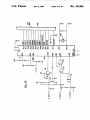
I I I l l l l l l l l l l l uml ?l wl l l l il l l l l l lI I Il l
United States Patent [19]
[11] E
Franklin et al.
[45] Reissued Date of Patent:
{54]
Patent Number: Re. 34,496
Jan. 4, 1994
APPARATUS AND METHOD FOR A
4,347,501
8/1982 Akerberg .......................... .. 340/539
CELLULAR FREEWAY EMERGENCY
4,371,751
2/ 1983 Hilligoss, Jr. et a1. ............. .. 379/41
TELEPHONE SERVICE
(List continued on next page.)
FORElGN PATENT DOCUMENTS
[75] Inventors: Philip G. Franklin; Scott Ward;
George R. Mabry, all of La Habra,
6084031 5/1985 Japan.
2114305 7/1983 United Kingdom.
Calif.
[73] Assignee: Cellular Communications
OTHER PUBLICATIONS
Eric S. Campbell, “Powers Radio Communications",
Communications, Oct. 1979, pp. 76-81.
Corporation, Irvine, Calif.
[2]] Appl. No.: 481,964
[22] Filed:
Primary Examiner-James L. Dwyer
Feb. 16, 1990
Assistant Examiner-Ahmad F. Matar
Attorney, Agent. or Firm-Nilsson, Wurst & Green
Related US. Patent Documents
Reissue of:
[57]
[64]
A self-contained cellular emergency roadside call box is
disclosed without the use of external telephone lines.
Patent No:
4,788,711
Issued:
Nov. 29, 1988
Appl. No.:
801,410
Filed:
Nov. 25, 1985
The call box is solar powered with battery storage and
comprises a controller coupled to a cellular transceiver.
The controller is also coupled to a solar array and bat
[51]
Int. Cl.5 .......................................... .. 1104M 11/00
[52]
U5. Cl. ...................................... .. 379/59; 379/63;
[58]
Field of Search ..................... .. 379/58, 59, 63, 38,
[56]
379/39, 40, 42, 45, 48, 51; 355/331, 313;
340/291, 287
References Cited
379/45; 455/331
3,207,849 9/1965 Andrews .
3,441,858 4/1969 Graham .
3,549,810 12/1970 Driscoll et a1. .
3,582,557 6/1971 Friberg et a1.
3,622,999 ll/l97l Getz, Jr. et a1. .
......... .. 379/40
.. 340/825.58
3,694,579
9/1972
McMurray
. . . . ..
3,800,089
3/1974
Reddick ............................ .. 379/388
. . . . ...
IMO/825.58
Carlson ................... ..
340/8251
4,092,600 5/1978 Zimmerman et al.
4,117,404 9/1978
4,131,849 12/1978
379/59
Marshall ............. ..
340/291
Freeberg et al. ..................... .. 375/5
4,176,254 11/1979 Turtle et a1. .
4,219,698 8/1980 Biriili et a1. .
4,338,493
7/1982
lished by the cellular transceiver to a cellular telecom
munication system. The cellular telecommunication
system includes a call site controller and mobile tele
phone switching terminal. Each call box comprises a
plurality of status subcircuits for monitoring conditions
mands required by the cellular transceiver. Information
3,844,840 10/1974 Bender .
3,912,875 10/1975 Kat: .
3,939,417 2/1976 Cannalte et a1. .
3,986,119 10/1976 Hemmer, Jr. et a]. ............... .. 455/9
8/1977
tery which is recharged through the controller. The call
boa communicates through a radio-telephone link estab
such as battery condition and transmitter status. The
call box communication and the status are processed by
a micro processor which generates appropriate com
U.S. PATENT DOCUMENTS
4,040,013
can be transmitted bidirectionally between each of the
call boxes and the communication applications proces
sor. An interactive flow of information is exchanged
with the call box and the functional condition is moni
tored.
REEXAMINATION RESULTS
The questions raised in reexamination request No.
90/002,066, ?led Jun. 25, 1990, have been considered
and the results thereof are reflected in this reissue patent
which constitutes the reexamination certi?cate required
by 35 U.S.C. 307 as provided in 37 CFR 1.570(e).
Stenhuis et al. .................... .. 379/38
1%!
ABSTRACT
10 Claims, 10 Drawing Sheets
R
“LU/Ml
r—— raw '—|
M1410!
Maw urn-“rum mom
Re. 34,496
Page 2
Metropolitan Transportation Commission, Freeway
U8. PATENT DOCUMENTS
4,406,995 9/1983 May ................................... .. 340/539
4,410,930 10/1983 Yachabach .
4,414,661 11/1983 Karlstrom ........................ .. 370/951
4,415,770 11/1983 Kai et a1. ..... ..
379/32
4,417,100 11/1983 Carlson et a1.
379/51
4,451,699
379/60
5/1984 Gruenberg .......... ..
4,465,904 8/ 1984 Gottsegen et a1. ................. .. 379/27
4,467,142 8/1984 Rupp et a1. ......................... .. 379/45
4,485,486 11/1984 Webb et a1. .
4,511,887
4/1985
Fiore ................................. .. 340/539
Harvey et a1. .................... .. 340/521
Callbox System, Report No. FHWA/RD-SO/IS], Nov.
1980, Final Report, pp. 1-116.
Cranston, T. K., et al., "Characteristics of Motorist Aid
Communications System,” IEEE Transactions on Vehic
ular Technology, vol. 19, No. 1, pp. 74-81 (Feb. 1970).
DeNigris, Ernest G., et a1. “Enhanced 911: emergency
calling with a plus,” Bell Laboratories Record, pp. 74-79
(Mar. 1980).
Fichaut, J. et al., "New Services for the IRT 1500 Sub
scriber Connection System,” Communication and
4,538,138
8/1985
4,577,182
3/1986 Millsap et a1. .
4,639,914
1/1987
4,675,863
4,724,538
5/1987 Paneth et a1. ....................... .. 370/50
2/1988 Farrell .
512," Ericsson Review, No. 3, pp. 158-163 (1982).
Komura, M. et al., "Subscriber Radio Telephone Sys
OTHER PUBLICATIONS
Frank .1. Mammano, "Driver Information and Motorist
Aid Hardware", IEEE Trans. on Vehicular Technol
ogy, vol. VT29, No. 2, May 1980, pp. 161-174.
Listing of cellular installations, Personal Communica
tions Technology, Feb. 1986, pp. 50, 52.
tem for Rural Areas,” Japan Telecommunications Re
view, vol. 18, No. 2, pp. 940: 11!) (Apr. 1976).
Winters .
Transmission, No. 2, pp. 25-38 (1985).
_
Janttl, Llkka, "Emergency Telephone System SOS
Rachel, 1., "Rural Radio Telephones with Solar Power
Supply," (pub. unknown) pp. 91-96.
Communication System", vol. 2.0 Cost Proposal Sup
Sanchez, A. Golderos, "Design of a multiple access
radio system for rural telephony,” Telecommunications
Journal, vol. 50, No. X1, pp. 615-621 (1983).
Vlamincky, 1..., “ATEA Police Call System," Hie Auto
matic Electric Technical Journal, vol. 4, No. 1, (Dec.
plement to Section 4.0.
1954).
"Motorist Aid Citizens Radio Service as a Wide Area
US. Patent
Jan. 4, 1994
Sheet 1 of 10
Re. 34,496
@@Q
Eh§3Q5\E
AT
Q
A
US. Patent
Jan. 4, 1994
Sheet 2 of 10
Re. 34,496
US. Patent
Jan. 4, 1994
Sheet 3 of 10
Re. 34,496 ‘
PD}; 1'? 0”
CA ‘L
4
I
sax
R
‘
“my
M457“
‘PM;
RESET
4:
7
051.4044};
c444 Bax
-*—-——-'
caur?auzn
6”
aurpur -
4‘)
‘do!
‘1
'
urn-Ry
20h“ Para/m
J2
czuumn
2”’
TRANSCi/ vm
Na
j YES
H‘ 4
READ
1/
47/!
.STA ms
215
nDOWN5
2/:
(‘ALL
Raw/Ne
.218)
(‘Au ‘mm-p’
ROUTINE
F74 /2
CALL
"EMRG f"
US. Patent
.nm. 4, 1994
Sheet 5 of 10
Re. 34,496
US. Patent
Jan. 4, 1994
Sheet 7 of 10
L»
Re. 34,496
L'
US. Patent
Jan. 4, 1994
Sheet 8 of 10
Re. 34,496
US. Patent
Jan. 4, 1994
Sheet 9 of 10
Re. 34,496
Lu
Q_wv
y
PM
W
W!
H H
H
aloqkE?
H
W‘
3
5
6
%
T
“35w>2.,
US. Patent
Jan. 4, 1994
w
i
Sheet 10 of 10
Q.
Re. 34,496
1
Re. 34,496
2
gency call boxes. A communication applications pro
APPARATUS AND METHOD FOR A CELLULAR
cessor is coupled to the cellular telecommunications
FREEWAY EMERGENCY TELEPHONE SERVICE
subsystem for processing data received in part from the
plurality of emergency call boxes. The communications
Mattereneloeedinhearybraekets [J appearalnthe 5 applications processor communicates through the cellu
original patent but forms no part ofthis reissue speci?ca
lar telecommunications subsystem with selected ones of
tion; matter printed in italics indicates the additions made
the plurality of emergency call boxes. By reason of this
by reissue.
combination of elements the plurality of emergency call
boxes can be installed and maintained at low cost and
BACKGROUND OF THE INVENTION
10 are capable of arbitrarily programmable interactive
1. Field of the Invention
operations.
The invention relates to the ?eld of cellular telephone
The system further comprises interof?ce local tele
equipment and in particular to solar powered telephone
phone exchanges coupled to the communication appli
call boxes using a cellular telephone system to radiotele
phonically communicate from a plurality of ?xed road
side sites.
2. Description of the Prior Art
Emergency roadside call boxes have become increas
cations processor wherein communication between the
plurality of emergency call boxes can be selectively
ingly important and productive elements in providing
coupled to the local telephone exchanges under control
of the communication applications processor.
The controller comprises a plurality of status subcir
cuits. Each status subcircuit monitors a predetermined
roadside security and emergency assistance in the met
status parameter of the corresponding call box.
ropolitan areas in the United States and throughout the
The system further comprises a circuit for selectively
world. Originally, such roadside emergency call boxes
communicating
the predetermined parameters as moni
were hardwired to conventional telephone land lines.
tored
by
the
plurality
of status subcircuits to the com
However, the installation of such telephone land lines
substantially escalates the installation and maintenance 25 munication applications processor. The parameters
monitored by the status subcircuits include battery
costs of such emergency roadside telephone boxes. In
power level, and the physical condition of the corre
order to overcome this limitation, the prior art devised
sponding call box indicative in part of whether call box
emergency telephone call boxes which use a radio
has been struck.
transmission link for communications. Cannalty et al.,
“Emergency Communications System", U.S. Pat. No. 30 The controller further comprises a circuit for receiv
3,939,417; and Wisniewski, “Emergency Calling Sys
tem", US. Pat. No. 3,492,581 show such systems.
ing and processing information from the communica
tion applications processor to initiate operations in the
controller.
The controller still further comprises a circuit for
35 adjusting the volume of transmitted and received audio
required the units to be coupled to a source of electrical
information.
power for trickle-charging or required the periodic
The controller has a timing mechanization included
replacement or recharging oi‘ the battery packs through
within its digital circuitry. The timer provides the capa
Power for the these call boxes is provided by a re
chargeable battery included within their housings.
However, such prior art battery operated systems either
mobile roadside service. Again, although savings were
realized in installation costs by using battery powered
units, the maintenance or service costs of such systems
often prohibited their use.
Furthermore, in the past radiotelephone communica
tions within geographic areas were realized using a
process based on a single transmitter and antenna. This 45
method of communication limits the number of calls
that can be placed in a geographic area and limits the
size of the area that can be covered with a given amount
of equipment. However, with the recent advent of cel
lular telephone technology, these limitations, which
were characteristic of the prior art single transmitter
systems, no longer exist.
Therefore, what is needed is a design and method of
using a radio linked emergency call box which is adapt
bility to measure predetermined elapsed time periods.
The timer mechanism is used in the following ways:
(1) To limit each call to a maximum duration (e.g. 10
minutes;
(2) To terminate a call if there is no conversation for
a predetermined period of time (e.g. one minute); and
(3) To cause each call box to automatically initiate a
call and to report its operational status on a periodic
basis (e.g. once every 24 hours).
In the event that the telephone handset is left oil‘ the
hook, the automatic time out will terminate the call and
will thus save battery power. Should this occur, the call
box is automatically reactivated and another emergency
call is placed should the hook switch be operated to the
on-hook status followed by an off-hook status.
able to cellular telephone technology and which is char 55 Stated in yet another way the invention is an emer
gency roadside call box comprising: a controller; a cel
acterized by low installation and service costs.
lular transceiver coupled to and controlled by the con
BRIEF SUMMARY OF THE INVENTION
The invention is a system for providing an emergency
troller; a battery for powering the controller coupled to
the controller and transceiver; and a solar array coupled
call box service comprising a plurality of emergency
call boxes, wherein each cell box further comprises: a
of this combination of elements an emergency roadside
to the controller for recharging the battery. By reason
call box can be installed and maintained at low cost.
controller; a cellular transceiver coupled to the control
The controller comprises a plurality of status subcir
ler; a battery coupled to the controller for providing
cuits for monitoring corresponding selective parameters
power to the controller and transceiver; and a solar
array for generating power coupled to the controller 65 of the controller, and a circuit for interrogating the
for recharging the battery. Also included in the system
plurality of status subcircuits for operationally respond
is a cellular telecommunications subsystem in radio
telecommunication with each of the plurality of emer
ing to the parameters as monitored by the status subcir
cuits.
3
Re. 34,496
The plurality of the subcircuits comprise at least a
subcircuit for monitoring a user request for emergency
4
FIG. 6 is a schematic diagram of another status sub
circuit.
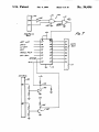
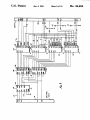
FIG. 7 is a schematic diagram of a circuit to read the
status data.
FIG. 8 is a schematic diagram of a programmable
transmission, battery condition, presence of a communi
cation transmitted to and from the call box, physical
integrity of the call box.
The call box further comprises a circuit for selec
microprocessor incorporated in the controller.
tively communicating the corresponding plurality of
FIG. 9 a schematic diagram of decoder circuit used
to communicate between the microprocessors on the
parameters of the call box to an off-site recipient.
The call box still further comprises a circuit for re
controller.
ceiving information generated off-site and a circuit for
initiating an operation of the call box in response to the
received off-site information.
The controller comprises a circuit for conserving
power from the battery when an emergency communi
cation is not desired, and a circuit for adjusting audio 15
gain for audio information transmitted and received by
the call box.
FIG. 10 is a schematic diagram of a circuit for cou
pling signals between the transceiver and one of the
microprocessors on the controller.
FIG. 11 is a schematic diagram of an audio level
adjust circuit which can be controlled by a remote
central processor.
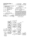
FIG. 12 is a flow diagram illustrating the operation of
the controller.
The invention and its various embodiments may be
better understood by now turning to the following de
The invention can still further be characterized as a
method in an emergency roadside call box, where the
call box is battery powered and coupled through a ra 20
scription.
die-telecommunication link to a cellular telecommuni
DETAILED DESCRIPTION OF THE
cation system and communication applications proces
PREFERRED EMBODIMENT
sor. The method comprises the steps of reading a plural
ity of call box status parameters. Next follows the step
Before considering the detailed circuitry in the cellu
of selectively performing a remedial routine in response 25 lar call box and its method of operation, first generally
to the step of reading the plurality of status parameters
consider the environment in which the call box is used
dependent upon the condition of each corresponding
and how it is utilized during normal operation.
parameter. Thereafter follows the step of selectively
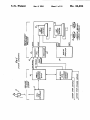
Turn now to FIG. 1. When an emergency occurs
entering an emergency call routine wherein a cellular
along a roadside, the affected user will locate the near
telecommunication transceiver within the call box is 30 est emergency call box, generally denoted by reference
powered up and bidirectional voice communication is
numeral 10. The user will lift the handset which will
established through the cellular telecommunication
cause call box 10 to automatically dial a prepro~
system to the communication applications processor.
grammed number to the freeway emergency telephone
By virtue of this method, remotely powered emergency
system control center. The call is transmitted via a radio
call boxes in radio-telecommunication with the commu 35 link to a local cell site transceiver 12 over a selected one
nication applications processor are operationally main
of 21 channels according to which channel is the stron
tained.
gest cellular channel available. This selection of com
The invention can still further be characterized as an
munication channels by transceiver 12 and mobile tele
phone switching of?ce 14 is well known in the art of
for generating information compatible with the cellular 40 cellular communications and will not be further de
radiotelephone in a solar powered emergency call box.
scribed. Local cell site transceiver 12 is connected with
The invention comprises a ?rst circuit for determining a
a mobile telephone switching office 16 by wireline
plurality of status conditions relating to the emergency
trunks. Mobile telephone switching office 14, which is
call box; a second circuit for controlling power usage of
an automatic terminal, then provides call box identity
the emergency call box to minimize power usage; and a 45 con?rmation and predialed access to the control center,
third circuit for processing the status conditions deter
which includes a communications applications proces
mined by the first circuit and responsive to at least the
sor generally denoted by reference numeral 16. Mobile
apparatus in combination with a cellular radiotelephone
status conditions controlling the second circuit. The
telephone switching office 14 can also connect call box
10 to a conventional telephone switching exchange 15
third circuit also selectively bidirectionally generates
and receives cellular radiotelephone compatible signals
in response to commands from the control center so that
under programmable control. The third circuit is cou
pled to the first and second circuit and to the cellular
three party telephone conference calls can be provided
or the call from call box 10 simply handed off to another
radiotelephone.
telephone station.
The invention is best understood in the context of an
illustrative example as shown in the following drawings
wherein like elements are referenced by like numerals.
55
BRIEF DESCRIPTION OF THE DRAWINGS
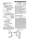
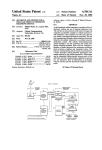
FIG. 1 is a block diagram of a system in which the
call box incorporating the invention is included.
60
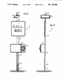
FIG. 2 is a front elevational depiction of the call box
as installed at a roadside site.
The incoming calls will be uniquely identified with a
speci?c emergency call box. The identification will then
be used to access a data base and all information corre
sponding to that call box will be retrieved in the appli
cations processor 16. An automatic call distributor 18
will connect the incoming call to an available operator
at a communications applications processor (CAP) sort
center 10. A human operator answers the call and the
communication which to this point has been digital will
be followed by voice communication. Specific call box
FIG. 3 is a side elevational view of the call box of
FIG. 1.
information will be displayed on the screen in response
FIG. 4 is a block diagram of including the controller 65 to an automatic call distributor processor 22 coupled
in the call box and its associated system elements.
with a master processor 24 which causes speci?c infor
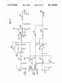
FIG. 5 is a schematic diagram of status subcircuits
mation to be brought up from the data base to the ap
included in the controller.
propriate support station 20. Such information includes
5
Re. 34,496
the location of the call box, nearest access roads, local
The modulated receive signal is then passed to a prom.
terrain and appropriate local emergency numbers. Sup
pli?er. A 3-pole ?lter, which further bandpass ?lters the
receive signal, is coupled to the output of the preampli
port station 20 and master processor 24 interactively
communicate so that all subsequent actions which are
?er. A ?rst mixer is coupled to the 3-pole ?lter. An
undertaken by the operator can be logged for archival,
injection signal is generated by a receiver synthesizer
management and planning use. Archival discs 26 are
coupled to and controlled by master processor 24 for
and mixes with the receive signal to provide a ?rst IF
signal. The IF signal is then coupled to an IF board.
The IF signal (45 MHz) is coupled to a buffer ampli?er
whose output is coupled to a Z-pole crystal ?lter which
mass data storage.
Turn now speci?cally to call box 10 as shown in FIG.
2 in front elevational view and in FIG. 3 in side eleva
tional view. Call box 10 is a completely self-contained
unit requiring no connection with external power lines
or telephone cables. Box 10 is solar powered, is de
signed for use with a cellular telephone system, and is
characterized by low-cost installation with quick repair
passes the signal on to a second buffer ampli?er. The
‘output of this buffer ampli?er is coupled to a second
Z-pole ?lter. The output of the second Z-pole ?lter is
coupled to a circuit which includes a second mixer, an
IF ampli?er, a receiver signal strength indicator, and a
PM detector. A second conversion and detection is
executed in this circuit and its output is an audio signal
which is coupled to an audio/logic board. On the audi
o/logic board the audio receive signal is conditioned in
or replacement.
As shown in FIGS. 2 and 3, call box 10 comprises a
housing 28 mounted on a road standard 30. Housing 28
includes the call box controller, radio transceiver and
a conventional manner.
battery described and shown diagrammatically in the 20 An audio signal from the handset is coupled to the
following Figures. The three watt radio transceiver is
radio via a transmit audio hybrid on the audio/logic
coupled to a conventional collinear antenna 32 with 3
board. This hybrid comprises a buffer and a 300 Hz to 3
dB of isotropic gain mounted on the top of standard 30.
kHz bandpass ?lter. The output from the bandpass ?lter
Also mounted with antenna 32 is a solar panel 34. Solar
of the transmit audio hybrid is fed to a 2:] compressor
panel 34 as described below is coupled to circuitry 25 comprised of by one half of a single IC compander
within main housing 28 and is used to recharge the
located on the audio/logic board. The compander dy
batter included within the housing. In particular, solar
namically condenses the audio signal, which is ex
array 34 is made of thirty-four matched silicon solar
panded 1:2 by the cell site controller to the original
cells with peak power rated at l0.5 watts. The panel is
dynamic range. The output of the compressor is fed
glass laminated and held in a metal frame to protect it
back into the transmit audio hybrid, which contains
from dirt, moisture and impact. Approximately 2.2 watt
circuitry for preemphasis, limiting, ?ltering, audio mut
hours per day is generated on the average by the solar
ing, and a summing ampli?er to combine the transmit
panel 34, which is equivalent to the amount of power
audio signal with data, supervisory audio tones and
for 45 minutes of constant air time, generally estimated
other control signals before outputting the signal to the
to be equal four to live average roadside emergency 35 synthesizer digital board. The transmit audio signal is
calls. Standard 30 is coupled to a ground anchor 36 to
coupled to the modulation input of a sidestep VCO on
embed it into the site. Ground anchor 36 and standard
the synthesizer board. The output of the VCO, a modu
30 are coupled together by brake plate 38 seen in FIG.
lated 30 MHz signal, is coupled to a buffer whose out
2 so that, if a vehicle collides with standard 30, brake
put is coupled to one input of a sidestep mixer. The
plate 38 will bend, retain standard 30 to the ground 40 injection input on the mixer is provided with a signal
anchor 36, and allow standard 30 to be folded over
which is an output frequency doubled from the receive
instead of being snapped over the hood and thrust
VCO. The output of the mixer is a modulated RF sig
through the windshield of the oncoming vehicle. Stan
nal. The RF signal is then coupled through a 3-pole
dard 30 is generally U-shaped so that the coupling an
?lter, and ampli?er before being coupled to a RF power
tenna and power lines between housing 28 and solar 45 ampli?er.
array 34 antenna 32 are laid in the U-shaped channel of
The frequency synthesizer comprises a receiver
standard 30 and can be covered or weather sealed by
VCO, a synthesizer digital board, and an exciter board.
protective plate 35. The entire unit therefore comprises
The operating frequencies in the radio are all derived
a sealed and weatherproof assembly.
from the receiver VCO phase-locked loop. This is com
The three watt cellular transceiver enclosed within 50 prised of a dual modulus prescaler, a programmable
main housing 28 is a conventional Motorola cellular
PLL IC, a charge pump, loop ?lter, and receiver VCO
hybrid. This loop is controlled by a channel select line
transceiver sold under the trademark, DYNA-TAK
2000. The details of operation of the transceiver are
from the logic circuitry which serially loads the channel
only implicitly included in this description and will not
select data into the programmable PLL [C One output
be expressly discussed except to the extent necessary for
of the receiver VCO goes through a frequency tripler
a fully illustrated description. Further details of the
and is fed to the injector doubler hybrid used in the ?rst
transceiver of the illustrated embodiment can be found
mixer of the RF receive circuitry. The other output
from the receive VCO is coupled to a frequency dou
in the published user's manual, entitled DYNA T.A.C.,
Cellular Mobile Telephone, 800 MHz Transceiver,
bler on the exciter boar and serves as the input signal to
available from Motorola Technical Writing Services at 60 the sidestep mixer.
1301 E. Algonquin Rd., Schaumburg, 111. 60196 which
Further details and schematics of all the above cir
is expressly incorporated herein by reference.
cuitry can be found in the Motorola User's manual
Although details of the transceiver are incidental to
referenced above.
the invention, a general description is provided here for
The transceiver signals which are referenced most
completeness of explanation. First consider the receive 65 often in the disclosure of the illustrated embodiment are
circuitry of the transceiver. In the transceiver discussed
the handset signals. The handset includes a cradle mi
croprocessor which provides an interface between the
in the illustrated embodiment, radio signals in a prede
termined range are selected by a 6-pole bandpass ?lter.
microprocessor of the handset and the microprocessor
7
Re. 34,496
of the transceiver logic unit. Digital communication is
(8) controlling all power for the entire assembly de
e?'ectuated through the digital signals C DATA, T
picted in FIG. 4 in a manner designed for the most
efficient conservation and use of power;
(9) interfacing to transceiver 44; and _
DATA and R DATA. Data carried by the bus conven
tion include keypad and ?uorescent display information
(10) providing necessary logic and interface for op
for the handset, display information for the cradle con
trol/indicator board, and other various control signals
and commands between the control unit and transceiver
logic unit. Only the more relevant of these signals will
be discussed below. Logic gates are provided in con
junction with the bus signals to gate either timing infor
tional controller functions and future enhancements
such as slow scan video or specialized data links.
Controller 42 is built around a microprocessor 118
described in connection with FIG. 8. A number of sig
nals indicative of the status of call box 10 are coupled to
a data bus 116 as described in FIG. 7 to which micro
mation or data depending on the state of a control line
INT SELECT. The handset processor uses this cir
cuitry to determine if the information on the T DATA
processor 116 is coupled and are generated by a plural
ity of status circuits described in FIGS. 5 and 6. Micro
processor 118 generates a number of discrete control
line is actual data or merely a timing pulse. C DATA
and T DATA, or C DATA and R DATA (the choice
depending on the direction of information flow) will be
signals through a decoder 130 (FIG. 6) for the control
of these status circuits and control signals which are
utilized in a decoder tree in FIG. 9 to provide key pad
logical complements during data transmission. When
they are not so related, they will signify timing informa
and other cellular control signals to cellular telephone
Handset 40 is diagrammatically depicted in FIG. 2.
functions can be provided by the circuitry illustrated.
transceiver 44.
tion, i.e. the reset or idle states. Communications with 20
Input and output to cellular telephone transceiver 44
these signals is on a three wire bidirectional bus. Data is
is completely effectuated by the keypad signals shown
communicated in an address-then-data serial word for
coupled to the input/output bus in FIG. 9 and by the
mat. At the beginning of communication the bus direc
digital signals, C DATA, T DATA, and R DATA
tion is established. During message transmission each
described below in connection with microprocessors
data state is followed by an idle state with a reset state 25 116 and 166. Cellular telephone transceiver 44 commu
entered after the last data bit of the message. Further
nicates with microprocessor 118 through a second or
details of the bus protocol are described in the Motorola
interfacing microprocessor 166 described in FIG. 10.
User's manual referenced above.
Both microprocessors I18 and 166 control the transmit
Keypad data is communicated from the handset via
and receive audio level control circuitry shown in FIG.
column and row signals which are then used with an 30 11. The overall operation of microprocessor 118 is sum
internal look-up table to identify the keypad button
marized by the ?ow chart of FIG. 12.
which was pushed.
Turn now to FIG. 5 wherein the operation of these
No further detailed discussion of the transceiver will be
FIGS. 5-7 are schematics of several circuits which are
undertaken except to such extent as such details affect 35 controllably used to sense a number of status conditions
of call box 10. For example, the charged condition of
battery 46, the physical integrity of call box 10, the
the operation of the cellular call box controller also
included in housing 28. The controller is a single board
circuit which can be easily removed from a modular pin
presence of information on the communication channel,
the status of handset 40, and the condition of the trans
vice. The controller comprises the logic and circuitry 40 mitter are all monitored and selectively reported by
means of the circuitry which will now be described in
necessary to control the entire operation of call box 10.
connector and a new board inserted for easy ?eld ser
connection with the following Figures.
Consider first the battery condition circuit depicted
Turning to FIG. 4, a diagrammatic depiction of the
elements within call box 10 is shown. Cellular call box
in FIG. 5. Battery 46 is coupled to node 50. A conven
controller 42 serves as the central unit to which solar
array 34, battery 46 and any additional call box switches 45 tional voltage regulator, generally denoted by reference
numeral 52 converts the 13 volts DC. to 5 volts for use
or input/output functions 48 are coupled. Similarly,
throughout the logic circuitry as indicated. The battery
cellular transceiver 44 is coupled to controller 42 and
voltage at node 50 is monitored by a conventional zener
antenna 32 in turn is coupled to cellular transceiver 44.
diode 54. If the voltage is sufficient, transistor 56, whose
Before describing the circuitry of controller 42, con
input is coupled to the anode of diode 54, will be biased
sider ?rst the functions which controller 42 performs.
on
and its output coupled through two inverters, collec
Included among, but not limited to these functions are:
tively denoted by reference numeral 58, to the set input
terminal SD, of a clocked latch 60. The output, Q, of
latch 60 is provided with the signal, inverted L0 BAT
(l) controlling operation sequences for user friendly
adaptation;
(2) automatically powering the transceiver when
handset 40 is lifted;
(3) automatically dialing the preprogrammed number
or alternatively any one of a plurality of numbers corre
sponding to one of a corresponding plurality of acti
vated switches or buttons (not shown in the Figures);
(4) automatically powering down after a preset, pre
programmed time period or after hang-up of handset 40;
(5) controlling and adjusting necessary voltage level
changes in audio and logic circuits;
(6) controlling and regulating all timing functions to
integrate the various portions of the assembly;
(7) controlling and regulating the recharging rates
from solar array 34;
55
(low battery), which is utilized in subsequent circuitry
as described below. Whenever LO BAT is true, a pre
determined low battery voltage or state of battery dis~
charged is indicated. The clock input, CP, of latch 60 is
provided with a signal, SET LO BAT (set low battery).
Latch 60 is cleared by a signal, CI. LO BAT (clear low
battery), coupled to the clear terminal, CD, of latch 60.
Consider now the circuitry in FIG. 5 which monitors
the physical condition of call box 10, namely whether
standard 30 is down on the ground. A mercury tilt
65 switch 62 is coupled between the five volt supply and
ground and is normally closed. However, should the
pole be struck, or otherwise tilted, switch 62 will open
as shown in FIG. 5. When switch 62 opens, a high or
9
Re. 34,496
10
true signal will be coupled to the set terminal, SD, of
DWN, LO BAT, BSY, TRANS PWR, and OFF LAT
clocked latch 64 whose output Q, is the signal, DWN
(down), representing that the pole is down. The clock
are each provided as inputs to an encoder 114. The
output of encoder 114 is coupled to a data bus 116 as a
parallel 8-bit word described in more detail in connec
input, CP, is the signal, SET DWN (set down), and
latch 64 is cleared at its clear terminal, CD, by the signal
CL DWN (clear down).
Turn now to the circuitry in FIG. 5 used to monitor
the status of the rf transmitter. When transceiver 44 is
turned on, 9 volts are applied to node 72. This in turns
on transistor 74 whose output is coupled through in
verter 76 to provide the signal, inverted TRANS PWR
(transmitter power), indicative that the transmitter is
powered up. Again, TRANS PWR is used in circuitry
to be described below as a status signal indicative of the
operation of call box 10.
Consider now the circuitry in E16. 5 used to selec
tively power up the rf transmitter, which as a primary
tion with FIG. 8. The remaining portions of the cir
cuitry of FIG. 7 will be described below.
Turning to FIG. 8, the encoded word in data bus 116,
which is diagrammatically shown throughout the cir
cuitry as appropriate, is coupled to inputs 80-87 of
microprocessor 118, which is the operational pro
grammed microprocessor of controller 42. Micro
processor 118 in the illustrated embodiment is a Motor
ola 6805 CMOS device which is characterized by very
low power consumption. Microprocessor 118 is
clocked by a conventional external crystal controlled
clocking circuit, generally denotai by reference nu
meral 119. The program for microprocessor 118 is
stored within an external EPROM memory 120. Mem
power user, is normally off. A signal, RLY ON (relay
ory 120 is accessed by microprocessor 118 through
on), generated by means described below, is applied to
a Darlington pair, generally denoted by reference nu 20 terminals B0-B7 and A8-A12, which provide a thir
teen-bit access word. Terminals 30-87 are used during
meral 94, to selectively energize a relay 96. When relay
the ?rst half cycle of processor 118 as the lower eight
96 is energized in response to RLY ON, the 13 volts of
bits of the address and during the second half cycle as a
power at node 50 is coupled through contacts 98 to a
plurality of power terminals ION SENSE, BAT PLUS,
data input-output. Therefore, during the memory fetch,
the lower eight bits of the address are coupled through
BAT PLUS TRANSCEIVER POWER, utilized else
where in the circuitry as an operative means of power
data bus 116 to a bit latch 122 under the control of the
ing up transceiver 44. These power voltages are particu
address strobe signal from terminal AS of processor
lar to the Motorola transceiver assumed in the illus
trated embodiment and are thus not further discussed
here.
Turning your attention to the circuitry of FIG. 6
consider now the status of the operation of handset 40.
The audio portion of the signal from handset 40 is cou
pled through capacitor 78 to a peak-to-peak detector,
generally denoted by reference numeral 80. The output
of peak-to-peak detector 80 is coupled through a buffer,
118. Thereafter, all thirteen bits of the address are cou
pled to address bus 124. The address inputs All-A10 of
memory 120 are thus coupled to address bus 124 and
memory 120 enabled by address bits A11 and A12
through NAND gate 126 and strobed by the output of
NAND gate 128. Memory 120 is selectively strobed in
a read or write cycle according to software control
through the read/write terminal, inverted R/W, and
data strobe terminal D5 of microprocessor 118 which
generally denoted by reference numeral 82, to the set
input, SD, of clocked latch 86. The output Q, of latch 86
is the signal, BSY (busy), which indicates that informa
are provided as the inputs to NAND gate 128.
Upon power up and reset the internal address register
of microprocessor 118 is set at the highest address of 2K
tion, conversation, or at least an audio signal of some 40 EPROM memory 120. The program is stored in two
kilobytes of memory. Thus A12 and All are provided
sort is being provided to handset 40. The clock input,
as the inputs to NAND gate 126 whose output is cou
CP, of latch 86 is the signal SET BSY (set busy) and
pled to the inverted chip enable terminal, CE. Thus the
latch 86 is cleared at its clear terminal, CD, by the sig
nal, CL BSY (clear busy).
two highest address bits serve as an address enable. The
The means for originating various status signals now 45 control and timing of microprocessor 118 with respect
to memory 120 is conventional and will not be further
having been described, the primary status signal,
detailed beyond that just outlined. At any rate, memory
namely the lifting of the handset off its hook switch, can
120 is appropriately strobed and stored information is
be considered. Conventional telephone hook switch 100
then read from outputs Q0-Q7 onto data bus 116. The
in FIG. 5 senses the lifting of handset 40. One terminal
signals data strobe, DS, and the read/write signal,
of the switch 100 is coupled to ground and the remain
R/W, from microprocessor 118 are similarly coupled to
ing terminal is coupled to a debounce NAND gate
the inputs of NAND gate 128, whose output then serves
latch, generally denoted by reference numeral 102. The
as an output enable signal coupled to the inverted out
output of latch 102 is the status signal, OFF LAT (off
put enable terminal of EPROM memory 120. Thus, data
latch), which is also used as a clocking signal for
clocked latch 106. The input, D, of latch 106 is coupled $5 from memory 120, as well as encoder 114, is appropri
ately made available to microprocessor 118 over data
to the 5-volt power supply so that upon receipt of a
bus 116.
clock pulse, OFF LAT, output Q of latch 106, the sig‘
Outputs PAO-PA7 and PRO-P87 are input/output
nal, OFF HK (off hook), goes high. Latch 106 is cleared
ports of microprocessor 118 which in the present em
at is clear terminal, CD, by a signal, CL OFF HK (clear
off hook). Thus once the handset has been taken off 60 bodiment are used only as output terminals which are
selectively accessed through a program control. Con
hook, the circuitry will be able to remember that this
sider now the various outputs provided at these termi
has occurred even if placed back on book until latch 106
nals. PA5-PA7 and PBS-PR7 are coupled to the inputs
is cleared by program control through CL OFF HK.
of decoder 130. The signals at the outputs of PA5-PA7
This allows the program to recognize that a call was
attempted and to enter a call ready status for a predeter 65 correspond respectively to two encoded bits designated
as ADA and AIA and an inverted enable signal, EA.
mined time regardless of the actual hook condition.
Similarly, signals PBS-P87 include respectively two
Turn now to FIG. 7. The various status signals de
encoded bits AOB and A18 together with an inverted
scribed in connection with FIGS. 5 and 6, OFF HK,
11
Re. 34,496
12
enable signal EB. These data bits and their respective
enable signals are thus coded according to conventional
coupled to data bus 116 according to the logic provided
by'gates 144. This logic prevents the placement of a
means into a plurality of control signals as illustrated in
status word on data bus 116 at the same time that the
FIG. 6. For example, the signals CL OFF HK, SET
BSY, CL BSY, SET DWN, CL DWN, SET LO BAT
program is being read from memory 120.
Turn now to FIG. 9 wherein signals Ail-A4, gener
and CL LO BAT which were described in connection
ated on control bus 132 by microprocessor 118 are con
with various status latches of FIG. 4 are generated by
verted into row and column key pad signals which can
microprocessor 118 in combination with decoder 130.
be understood by transceiver 44. The signal A4 on con
The various latches are thus clocked and cleared at the
trol bus 132 corresponding to the output from terminal
appropriate times under software control as the status of 10 PA4 of microprocessor 118 is an enable signal used to
call box 10 queried.
enable decoder 154. Decoder 154 is driven by the con
Outputs PAO-PA4 of microprocessor 118 are cou
trol signals A2 and A3 corresponding respectively to
pled to a control bus 132 to respectively generate con
terminals PA2-3 of microprocessor 118. The output of
trol signals Ali-A4 whose use will be better described in
decoder 154 are intermediate inverted decoding signals
connection with FIG. 10 in relation to the manipulation
EA and EB. These signals are output in parallel to a
of transceiver 44.
second stage of two decoders 156 which have as addi
The output of PB] of microprocessor 118, which is
active low, is coupled to an inverter 134 whose output
136 is a signal, RLY ON, used to power Darlington pair
94 in FIG. 5 in order to power up transceiver 44.
PA7, P87, and P81 are each pulled high through a
resistor in the case where the lines ?oat so that decoder
130 and the transceiver power up relay are affirmatively
maintained disabled unless clearly pulled active low by
an appropriate output on each of these lines.
tional inputs, control bus signals A0 and A1 correspond
ing respectively to terminals PAD-1 of microprocessor
118. Ultimately the ?ve control bits All-A4 will be
converted into twelve key pad signals corresponding to
the twelve buttons on a telephone key pad correspond
ing to digits 0-9,’ and #, and two additional related
radiotelephone signals ON/OFF and volume control,
VOL CONT. Thus, bits Ail-A3 represent sixteen possi
25 ble combinations with a four-bit word which is decoded
The outputs of PEG-P33 of microprocessor 118 are
the signals, return data transmit, R DATA T; receive
data receive, R DATA R; true data receive, T DATA
sixteen discrete output signals to the inputs of analog
R and inverted interrupt control, INT-CONT, which
outputs or enables the one of sixteen outputs as desig
are speci?c input and output control signals used to
provide necessary control functions for transceiver 44.
nated by the Ail-A3 bits. Consider for example analog
switch 164. The four inputs to analog switch 164 corre
spond to the key pad numerals 0-3. With respect to each
of these numerals, two signals will need to be generated
in order to command transceiver 44, namely the row
Coupling directly to the input/output ports PBll-PBS
of microprocessor 118 gives the microprocessor the
in two stages in decoders 154 and 156 and coupled as
switches 158-164. The A4 bit either disables all sixteen
ability to directly respond to and to manipulate a trans
ceiver if desired. However, in the present embodiment, 35 and column designations corresponding to key pad
these control ports are not speci?cally used for the
numbers 0-3. In particular, numeral 0 is located in the
Motorola transceiver illustrated.
second column and fourth row. Therefore, the ?rst two
Returning to FIG. 7, output PB] of microprocessor
outputs of analog switch 164 correspond to column 2,
166, to be described below, is also coupled to an input
row 4 will be activated in response to activation of one
/output bus 138. P31 is coupled from input/output bus 40 of the inputs to analog switch 164, such as E0. The pairs
138 to an inverter, generally denoted by reference nu
of outputs corresponding to numerals l, 2 and 3 are
meral 140. The inverted PB! signal is applied to node
similarly activated. In the same manner the outputs of
142 as the signal, SVC (service), indicating that the
analog switch 162 correspond to the row and column
transceiver has established radiotelephone contact with
pairs corresponding to key pad numerals 4-7. Analog
a ground station. The signal, SVC, is then coupled to 45 switch 164 similarly includes as its outputs key pad
one of the inputs of encoder 114 and used as a condi
numerals 8 and 9, ' and #. The outputs of analog switch
tional signal to generate the eight bit status words cou
158 are peculiar to radiotelephones, which comprise a
pled from encoder 114 to data bus 116.
fifth row. The ?fth row on a radio telephone corre
The output PB7 of microprocessor 166, to be de
sponds in the second column to the signal END and in
scribed below, is similarly coupled to input/output bus 50 third column to the signal SND. Included as discrete
138 to an inverter generally denoted by reference nu
signals are the control signals volume, VOL, and
meral 152. Output 154 from inverter 152 is the inverted
power, PWR, which are also referenced in FIG. 9 as
signal, IN USE, which is used to signify that a call has
the input/output signals on bus 138 as VOL CONT and
been placed or is in process. Thus IN USE similarly can
ON/OFF, respectively. Each of the row and column
be used as a conditional signal in decoder 114 to prevent 55 signals from switches 156-164 are active low and are
inappropriate transmission of a status word to data bus
116.
Encoder 114 is also coupled to the two highest ad
dress bits A11 and A12 from address bus 124 through a
appropriately buffered and coupled through diodes and
resistors according to conventional principles as illus
trated in FIG. 9 to I/O bus 138. By this means micro
processor 118 can be arbitrarily manipulate and control
series of logic gates, generally denoted by reference 60 radiotelephone transceiver 44.
numeral 144. More particularly, A12 is inverted by
Turning how to FIG. 10, a microprocessor 166, run
inverter 146 and coupled together with address signal
by crystal controlled clock 16!, allows signals received
A11 to the inputs of NAND gate 148. The output of
by transceiver 44 to the place signals of the input/out
NAND gate 148 is logically combined in OR gate 150
put bus 138. Microprocessor 166 interfaces the circuitry
with the output of NAND gate 128, the inverted signal 65 and buses described above with the unique signals used
DS/R. The output of OR gate 150 in turn is coupled to
by transceiver 44 and to that extent is transceiver de
the inverted output enable terminal, OE, of encoder
pendent. The signals, return data, R DATA; comple
114. Therefore, the output word from encoder 114 is
mentary data, C DATA; and true data, T DATA are
13‘
Re. 34,496
signals speci?c to the Motorola transceiver 44 and are
digital signals which are transmitted between trans
ceiver 44 and the controller.
Each of these signals is coupled through appropriate
logic circuits to input ports of the microprocessor 166.
For example, T DATA, an input signal to microproces
sor 166, is coupled through an exclusive OR gate 170
acting as a buffer since one input is held low. The output
of gate 170, which is T DATA, is also coupled to input
port PR4 of microprocessor 166. C DATA and buffered
T DATA output from gate 170 are provided as the
inputs to exclusive OR gate 172. The output of gate 172
14
read the R DATA line through gate 176 and compare it
with what is being sent. If there is a conflict, processor
166 will stop sending and vacate the bus. Processor 166
will request service again when the bus returns to the
idle state.
Consider now the remaining output terminals of mi
croprocessor 166. The outputs PCO-PC2 correspond to
columns 3 through column I of the key pad respec
tively; outputs PAO-PA4 corresponding to rows 1-5 of
the ltey pad respectively; and signals PB] or SVC (ser
vice), and P137 or IN USE described above can be selec
tively generated coupled to input/output bus 138. PA7
is a GAIN ADJ signal described below in connection
with FIG. 11 used to adjust audio signal strengths in the
false. Thus, the output of gate 172 is true whenever data 15 voice channel. PC3 is coupled to a push button switch
is being transmitted on the three wire bus and is false
which can be manually operated by the call box user to
when the bus is in the idle state or reset state. The out
step up the audio strength of the received voice commu
put of gate 172 is provided as an input in turn to exclu
nication.
aive OR gate 174 whose other input is coupled to an
Turn now to FIG. 11 wherein the circuitry illustra
interrupt port P83 of microprocessor 166. The output 20 tive of audio processing is illustrated. The microphone
of gate 174 is coupled to the inverted interrupted termi
input of hand set 40 is coupled across terminals 180. The
nal, INT, of microprocessor 166. This terminal will be
audio signal for the caller is thereby coupled through
active whenever data is being received from the trans
coupling capacitor 182 to an audio ampli?er, generally
ceiver. P133 port acts as an internal acknowledgement
referenced by numeral 184. The output of audio ampli
signal. The output of gate 172 will be low when the data 25 fter 184 is coupled through coupling capacitor 186 and
link is the idle and will be high when it is busy. There
provided as an output at node 188 as the transmitted
fore when P83 is high, the inverted interrupt, INT, will
audio, TX AUDIO.
go active low when data comes in. This will cause an
ON/OFF is a toggle signal on V0 bus 138 as de
interrupt to be executed in microprocessor 166 to enable
scribed in FIG. 7 and is similarly coupled through limit
it to receive data.
30 ing resistor 190 to node 188 to override the transmitted
Finally, R DATA is similarly coupled to the output
audio signal according to microprocessor 166 to cause
of transistor 178. Transistor 178 is in turn driven by
the transceiver to be turned on or off. Thus, grounding
is thus true whenever T DATA or C DATA are true
but if in an idle state they both go true, the output is
output P80, which is the data output from microproces
sor 166 to transceiver 44. An input of exclusive OR gate
176 is also coupled to the output of transistor 178 and
gate 176 acts as a buffer. Therefore, the output of buffer
gate 176 is the signal, R DATA, which is applied to
input port PHI for the purposes of timing.
Consider brie?y the timing protocol used on the
the on/off line at V0 bus 138 causes the transceiver
power to be turned on if it is off or to be turned off if it
is on.
Similarly, audio volume control or a gain adjust sig
nal, GAIN ADJ, is provided from I/O bus 138 through
signal PA7 of microprocessor 166. This is a gain adjust
signal coupled through transistors 190 and 192 thereby
three wire bus. Normally, the bus is in a reset state, i.e. 40 biasing node 194 at the input side of audio capacitor 182
C DATA and T DATA are both false. when either one
to a point appropriate with the desired audio gain. Thus,
changes microprocessor 166 will be interrupted. The
the remote central controller can advise call box 10 to
message appearing on the T DATA line contains a bus
turn up the microphone volume as needed through the
direction ?eld, destination address ?eld and data ?eld.
When microprocessor 166 initiates communication, R
manipulation of the T, and C DATA signals coupled to
microprocessor 166 which then appropriately generates
DATA data will go low indicating a request from pro
cessor 166. A logic unit in the transceiver will establish
the gain adjust signal, PA7.
bus direction and will expect to receive a message on
Similarly, the received audio from the remote central
operator is coupled terminal 196. Again, the received
the R DATA line. The message then display on R
audio signal is coupled through an audio capacitor 198
DATA includes a source address ?eld, destination ?eld
into an audio ampli?er generally denoted as reference
numeral 200. The feedback of audio ampli?er 200 in
turn is controlled through the transistor 202 by means of
and data ?eld. When the request for service is answered
by the transceiver, processor 166 will read the R
DATA line and the destination address ?eld of the
the gain adjust signal, GAIN ADJ, acting through the
incoming message. Processor 166 will place a ?rst bit of
output transistor 190. Therefore, the received audio
R DATA on the line at the start of a data state. During 55 gain coupled to input 204 of differential ampli?er 206
communication
by the transceiver the ?rst data
can be remotely operator adjusted through gain adjust
bit will appear on the R DATA line after the bus goes
signal GAIN ADJ. The output of differential ampli?er
206 in turn is coupled to the input of a push/pull ampli
from the reset state to the date state. The remaining data
will appear on the R DATA line during the idle state to
?er generally denoted by reference numeral 208. The
data state transition period. The last data bit of the 60 output of push/pull ampli?er 208 is coupled as the op
message will be held on the R DATA line a few micro
posing input to differential ampli?er 206 thereby main
seconds after the T DATA and C DATA lines have
taining the output 210 of differential ampli?er 206 at a
continual maximum. The output of push/pull ampli?er
208 is in turn resistively coupled through audio capaci
returned to the reset state to allow the bit to be read by
the control unit. During a communication initiated by
processor 166, processor 166 will hold the ?rst data bit 65 tor 212 to the receiver or car piece terminals 214 in hand
set 40.
on the R DATA line until T DATA and C DATA lines
Solar array 34 is also coupled to battery 46 through
enter a data state at which time another bit is sent. At
controller 42 by means of a shunt regulator. The regula
the occurrence of each idle state, processor 166 will
15
Re. 34,496
16
tor is conventional and thus is not further shown in the
Figures. Coupling through the shunt regulator prevents
overcharging of battery 46 and thereby eliminates the
potential of any damage due to overvoltages or over
charging.
The circuitry now having been generally described in
connection with FIGS. 4-9, turn to the flow diagram of
FIG. 12 which illustrates the basic operation of control
ler 42. Upon power-up as indicted by step 201, a master
reset signal is generated to program control at step 203
to reset all chips within the circuit. This step generates
any logic reset signals required by the microprocessors
118 or 166 or any other logic
In addition
during this step the transceiver may execute any initial
protocol operations. For example, in the case of the
Motorola transceiver of the illustrated embodiment, the
best ground station or forward control channel is se
lected. Service is then established between the selected
forward control channel and the call box. The trans
ceiver or microprocessor 118 then dials a prepro 20
grammed telephone number and sends identifying codes
four~hour ?ag. If a twenty-four-hour interval has not
expired since step 224 was last queried, the processing
will return to step 210. If on the other hand, twenty-four
hours have elapsed since the last query at step 224, a call
report status routine is entered at step 226. At step 226.
microprocessor 118 will enter a predetermined subpro
gram to telephone the central processing unit regarding
the status of call box 10. Thus, every twenty-four hours
or on any other arbitrary schedule, each call box will
call the central processing center, identify itself and
report its current status or even a past log of activity.
Many modi?cations or alterations may be made by
those having ordinary skill in the art without departing
from the spirit and scope of the invention. For example,
the operational routine described at FIG. 10 is illustra
live only and any other means could be arbitrarily pro
grammed into execution. It is to be expressly under
stood that a different cellular transceiver, such as an
OK] model UM l043B manufactured by OKI Electric
Industries Co. Ltd of Atlanta, Ga, could be easily sub
which establish the call box’s identity. These numbers
stituted for the illustrated Motorola transceiver with
appropriate modi?cations to accommodate the substitu
and codes are veri?ed and then communications is se
lectively established on a reverse channel when appro
tion according to well know design principles.
Furthermore, it should be noted in connection with
priate. All this is protocol which is normally handled by 25 the circuit diagrams of FIGS. 4-9 that call box 10 incor
the cellular transceiver and ground station and do not
strictly affect the operation of the invention as de
scribed here.
‘Thereafter, the outputs of each of the status chips are
set to zero or initialized at step 205. This corresponds to
porstes a digital address bus, data bus, control bus and
1/0 bus. Therefore, it is entirely within the scope of the
art that such generalized bus structures can be em
ployed with other digital circuitry to expand the opera
tional capacities of call box 10. For example, a slow scan
the generation of various set signals shown as the output
video circuit can be appropriately coupled to the buses
if desired to provide visual information of tratl'ic condi
latches of FIG. 8.
tions at selected points. In addition, a data telemetry
Having cleared and set each of the status latches,
input subcircuit can similarly be coupled to the buses of
processor 118 then enters a self-test program to test the 35 call box 10 to allow, for example, for the transmission of
contents of memory 120 at step 207. Each self-test pro
digital medical data by paramedical emergency teams
gram is checked a predetermined plurality of times at
who may be attending an accident victim near the site
step 209. The test is repeated until it successfully passes
of a call box. Such emergency medical data could be
of decoder 130 and as described in connection with the
or a timeout occurs. Upon successful self-testing of
radio-telemetered from the accident site to the nearest
memory 120, processor 118 will then read the various 40 call box which would then retransmit to the nearest
status signals as step 211 as described in connection with
hospital without the necessity of lifting hand set 40 off
FIG. 5. Should the pole down signal, DWN, for exam
the hook or other direct wire coupling to the call box.
ple, be active as determined at step 213, processor 118
The call box could similarly be time share with environ
will then enter a specialized down routine at step 215 to
mental sensing and reporting systems. Virtually any
take whatever appropriate remedial action or reporting 45 device which could bene?t from a remote communica
asisdesiredinthecmethatthecallboxhasbeenrun
tions device could be easily combined and accommo
over or otherwise down on the ground.
dated by the open bus structure of the invention. The
After the down routine is completed, or there is no
adaptability of the invention is even further enhanced
pole down situation, processor 118 then determines at
when it is realized that interactive digital and voice
step 216 whether the battery level is low. If the power 50 communications is facilitated through call box 10.
is low, it enters a power subroutine at step 218 and
performs any remedial action necessary in response to
low battery, such as unconditionally disabling the trans
ceiver 44. Again, after execution of the low power
routine or if the power is adequate, microprocessor 118
will then inquire at step 220 whether an emergency call
is being placed. If an emergency caller is placing a call
by lifting hand set 40 off the hook, an emergency call
routine is entered at step 222 wherein transceiver 44 is
powered up, a predetermined phone number is dialed or
transmitted, together with speci?c identifying informa
tion uniquely identifying call box 10. After the call is
completed, the processing again returns to step 210
where the status is reread.
If at step 220 an emergency call is not being placed, 65
an inquiry will be made at step 224 as to whether or not
a predetermined time interval has passed. In the illus
trated embodiment call box 10 incorporates a twenty
7 Therefore, the illustrated embodiment must be under~
stood as being provided only for the purposes of exam
ple and clarity and not as a limitation of the invention as
de?ned in the following claims.
I claim:
1. A system for emergency call box service compris
mg:
a plurality of emergency call boxes, wherein each call
box further comprises a controller, a cellular trans
ceiver coupled to said controller, a battery coupled
to said controller for providing power to said con
troller and transceiver, and means for generating
power coupled to said controller for recharging
said battery; and
cellular telecommunications subsystem in radio
telecommunication with each of said plurality of
emergency call boxes [,]:
said cellular transceiver being remotely [program