1
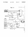
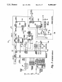
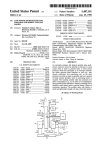
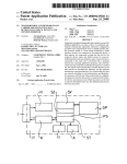
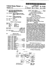
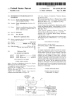
llllllllllllllllllllllllllllilllllllllllllllllllllllIllllllllllllllllllllll
.
US005305467A
Unlted States Patent [19]
[11] Patent Number:
Herndon et al.
[45]
[54]
[75]
Apr. 19, 1994
LOCAL AREA NETWORK FOR FLEXIBLE
4,684,941
8/l987 Smith ........................... .. 340/825.52
DIGITAL COMMUNICATIONS WITHIN
4,686,671
8/1987 Burian et a].
4,726,050
2/1988
Menich ............................... .. 455/33
4,918,746
8/ 1990
Serizawa .......................... .. 455/561
AND BETWEEN RF BASE STATIONS
Inventors: Charles C. Herndon, Forest; John R.
Martin, Lynchburg; Rodney L.
Lynchburg; Daniel I.
.
8“
’
’
4,993,059 2/1991 Smith .................. .. 455/33
'
5,081,641
[73] Assignee: ?rzcsslosnglliblzliptgiblgeaCommumcanons
-’
y
.
..
1/1992
Kotzin et al. ..... ..
455/331
FOREIGN PATENT DOCUMENTS
'
Appl No _ 620 423
.
..... ._ 455/341
4,730,187 3/1988 Menich et al. .
4,789,983 12/1988 Acampora et al. ................. .. 370/84
4,866,710 9/1989 Schaeffer ............................ .. 455/33
DiSSOSWay Ct a1. .
zcihwifl?’ l?gfej‘t‘bggé?‘fame I"
[2]]
Date of Patent:
5,305,467
3638735
5/ 1988 Fed. Rep. of Germany ...... .. 455/89
,
_
Primary Examiner-Reinhard J. Eisenzopf
[22]
[51]
Flled'
Dec' 3’ 1990
Int. Cl.5 ............................................ .. H04B 3/00
Assistant Examiner—-Chi Pham
Attorney, Agent, or Firm-Nixon & Vanderhye
[52]
US. Cl. ................................ .. 455/561; 455/671;
[58]
Field of Search .................... .. 455/73, 75, 89, 5,1,
455/56.l, 34-1, 331, 54-1, 53-1, 67-1, 49-1, 38-1;
A LAN multi-node generic digital signal communica
tions link within a radio frequency (RF) base station
370/95.1, 85.1, 35-2, 35-3; 379/ 58; 375/ 36;
340/825-52
system communicates control signals within and be
tween base stations. The generic digital signal link elim
370/85.1; 379/58
[56]
[57]
‘
ABSTRACT
References Cited
rates
thehuse of multiple lines for .respectiye futnctioins
y us1ng ‘t e same generic commumcations inter ace or
us‘ PATENT DOCUMENTS
various different functions. By using such a generic
4,584,678 4/1986 Ozeki et al. ...................... .. 370/85.3
4,587,651 5/1986 Nelson et a1. .................. .. 370/85.l3
signal
for inter and intra base Station commu
nic?tions’ RF and auxiliary comm] become Standap
ags/$1“? 31' '
dized-reducing complexity in the product, in the doc
455/89
4:608:70O
8/1986 Kirtley, Jr. et al. ............. .. 370/85.2
4,636,791
l/l987
4,667,191
5/ 1987 Comroe et a! ...................... .. 455/73
umemam" and 1“ ?eld re1m" techmques
Burke et ai. .
10 Claims, 7 Drawing Sheets
' _____________________ "I
=l
WY
1
. 24
i
Y
1
RF
I
'
RCVR
|
seuoms
TRANSCEIV ER
/22
RCVD
:
INTERFACE
36
213
(P:_
12\ l
I"2
DISPATCH
1 TL
1 TL
I
12“
12B
:
I
~m" :
19
crcss
c'nzss
3mm
FILTER
:
(32
:
l
I“
:
:
FILTER
so
$55M
n
N
on
112"
‘I
DlglTAL
5' ML
PROCESSING \34
|
1
. REPEATER BASE STATION
Y
RECEIVIMEVER
5.2%}; "G I ___
CONTROL|
l
L I1
>-- east
:
B
l
'
:
$856014
A
|
‘‘
10/
CONSOLE
i $151014
I
1
53
)
\wmo
* 1
XMITTER ‘T’ MODULE 8 :
mLER \irgo
:
5
RF
1 /50
20c~ 2504’ "1288 \ZZa
:
m
|"'"".
52'1"???“
i
|
“1
COMBINER
20\
LAN
“'11s. .5” '
x
i
51
'
'
:
1
I
I
l
J
i
S
14b
10
US. Patent
Apr. 19,1994
FROM FIG. 2a
Sheet 4 of 7
‘
is
5,305,467
2 C
GSC
ALE---—>
892255100».
DSP ADDR
ADQ -7
009-7
LATCHED
l/O
PPI
AG
I
CS
‘m
RF
TO LINE
SEL. TX
SEL.
__1
I
I TO MODEM 48
OR
|
I
HANDSET 52
US. Patent
(
Apr. 19, 1994
Sheet 7 of 7
START )
5,305,467
START
410
4QO\ INITIALIZE
GSC
M33
N
?
Y
GET NEW
4°2'\ FREQUENCY
RCV
\412
MESSAGE
414
oouvsn'r TO
404\ PRESCALER
~
4,6
FORMAT
(
Y
PROCESS
MESSAGE
SELECT
406
\
BUILD MSG
m BUFFER
TX
SYNTH
\41a
TRANSMIT DATA
4°8\ SEND M36
OVER LAN
DONE
CONTROLLER
Fig. 5A 28
TO PI>"‘ESCALERF\"'2o
3°4
INTERFACE Moouua
5,305,467
1
2
section may monitor received signal strength and/or
LOCAL AREA NETWORK FOR FLEXIBLE
DIGITAL COMMUNICATIONS WITHIN AND
BETWEEN RF BASE STATIONS
carrier detect, DC input current to the transmitter ?nal
ampli?er, etc.).
CROSS-REFERENCES TO RELATED
_
APPLICATIONS
'
In the past, such control and status signals have been
communicated between the control section and the RF
section over an array of dedicated parallel conductors.
One typical con?guration used in the past was to pro
vide the RF section and the control section each with a
multipin connector. A multiconductor cable (or, in
'
This application is related to the following common
ly-assigned copending patent applications (all of the
disclosures of which are hereby incorporated by refer
some cases, a bus backplane) was used to convey, in
ence herein):
US. application Ser. No. 07/596,357 now abandoned
parallel, all of the various signals that needed to be
communicated between the RF section and the control
of Vignali et al ?led Oct. 12, 1990 entitled “A Full
section. For example, one or more conductors might be
Duplex RF Repeater/Base Station Providing Mi
croprocessor-controlled Simultaneous CTCSS
Tone Encode/Decode”;
dedicated to carrying a signal generated by the control
section for controlling whether or not the transmitter in
the RF section is keyed; one or more further conductors
US application Ser. No. 07/620,422 now abandoned
might be dedicated to carrying frequency programming
of Herndon et al ?led concurrently herewith enti
control signals from the control section to the receiver
tled “Remote Control of RF Base Station Via Digi
frequency synthesizer in the RF section, one or more
20
tal Communications”; and
still further conductors might be dedicated to carrying
US. application Ser. No. 07/620,421 of Nickel 'al a1
control signals from the control section for program
?led concurrently herewith entitled “Digital Sig
ming the transmitter frequency synthesizer, etc.).
Although such dedicated parallel conductor-type
nal Processor for Radio Base Station”.
interconnection arrangements work, they have certain
FIELD OF THE INVENTION
25
disadvantages. One disadvantage of such prior art inter
The present invention relates to radio frequency (RF)
connection arrangements is the relatively high cost.
repeating type transceivers of the type which transmit
Multipin connectors and associated cables are expen
and receive radio frequency signals, and more particu
larly to so-called Base Station RF transceivers. Still
sive. Moreover, since radio frequency signals and digi
niques and arrangements for communicating digital
precautions must be taken to minimize RF currents
?owing on each such conductor. Each such conductor
had to be “RF decoupled” at both the RF section end
and the control section end using RF shunting and/or
tal control signals are not compatible with one another,
more particularly, the present invention relates to tech 30
control signals within and between such RF base sta
trons.
BACKGROUND AND SUMMARY OF THE
INVENTION
35
bypass networks (e.g., series-connected RF chokes and
shunt-to-ground decoupling capacitors). Since each
individual conductor had to include an RF decoupling
Many modern radio frequency (RF) base stations
network at each end, RF decoupling added signi?cantly
have separate RF and control sections. A base station
to the cost and complexity of the base station.
RF section typically includes mostly analog circuitry
(e.g., RF ampli?ers, RF oscillators, RF and IF receiver 40 In addition, such parallel dedicated conductor inter
connections created reliability and service problems.
ampli?ers/?lters, etc.) Most modern RF base stations
Reliability problems are created whenever an additional
available today control such an RF section with a digi
mechanical-type electrical connection is introduced.
tal (e.g., microprocessor based) control section. Such a
Such connections can corrode or otherwise mechani
digital control section can provide expanded control
capabilities and ?exibility, thereby providing many
45
cally deteriorate, degrading or destroying critical inter
advantages over prior analog control circuit arrange
connections between the RF section and the control
ments.
section. Preventive maintenance efforts had to be ex
pended to ensure such connections were properly main
As is well known, digital circuits are not particularly
tained. As the number of conductors increased, the
compatible with RF signals. The RF section of a base
station is therefore almost always housed in a separate 50 complexity of testing for and isolating base stations
faults also increased (thus increasing down time and
shielded enclosure to prevent RF signals radiated di
rectly by the power ampli?er and other components
therein from reaching the sensitive digital circuitry and
vice versa (digital circuitry getting into receiver).
service time).
Still further complexity is introduced by the require
ment that most RF base stations must supply their cus
Interconnecting the RF section with the control sec 55 tomers with a wide variety of different base station
options. The Federal Communications Commission
tion is typically a relatively dif?cult and signi?cant
authorizes base station operation on a user-by-user basis.
problem. A relatively large number of signals must pass
Such authorizations specify different operating frequen
between the RF section and the control section. For
example, the control section may typically program the
operating frequencies of the transmitter and the re
cies for different users, and may typically also specify
different RF output powers for different users. One user
may be authorized to operate with only, say, 100 watts
of RF power, where as another user may be authorized
ceiver within the RF section and may also directly
control various other parameters of RF section opera
to operate with several hundred watts of output power
tion (e.g., whether or not the transmitter is'keyed, the
state of an RF antenna relay, the transmitter ?nal ampli
(different antenna configuration can also affect the
?er power output, etc.). In addition, the control section 65 power output required by a base station transmitter).
must monitor various status and other parameters pro
The user needing only relatively low output power
vided by the RF section in order to ascertain the state of
should not have to buy a base station having relatively
operation of the RF section. For example, the control
high RF output power capability, since the high-pow
3
5,305,467
4
ered components are generally more expensive and
drastically increase the cost of the base station. Thus,
for marketing and other reasons, base station manufac
turers found it necessary to provide different RF output
802.3 LAN Standard 1.0 MBps). The Intel 80Cl52 was
thus designed to make it possible to implement a LAN
by merely more or less directly interconnecting 80Cl52
power options for their base stations. Similarly, differ
ceiver ICs to transmit and receive the serial data).
Digital signal serial links are not unknown in the
world of RF systems. For example, it is generally
known to interconnect a digital controller with RF
microcontrollers together (using appropriate trans
ent users may be assigned by the FCC to operate on
completely different bands within the RF spectrum. RF
circuitry designed for operation on a relatively low
(e.g., several hundred megahertz) RF frequency is not
capable of operating at high (e.g., 800 or 900 MH) RF
components within a mobile radio transceiver using a
frequencies. Accordingly, to meet the needs of a wide
serial communications link. See, for example, US Pat.
No. 4,903,262 issued 20 Feb. 1990 entitled "Hardware
variety of users, a base station manufacturer must pro
Interface and Protocol for A Mobile Radio Trans
ceiver"; and copending divisional application thereof
Ser. No. 07/449,790 filed 15 Dec. 1989 now US. Pat.
and for different power output levels.
Perhaps the most economic way for a base station 5 No. 5,109,543. See also US. Pat. No. 4,590,472 to Ben
vide different base stations for different operating bands
manufacturer to meet such a wide variety of customer
needs is to make different RF sections for different RF
son et al; US. Pat. No. 4,636,791 to Burke et al; and US
Pat. No. 4,684,941 to Smith et al. In addition, commonly
output powers, frequencies of operation, etc., and to
make his control section mostly generic with respect to
assigned U.S. patent application Ser. No. 07/532,164
all such different RF sections. Thus, each of the RF
sections can be made to be "plug compatible" with the
same control section. While such an arrangement is
both possible and practical, it introduces further com
“Fail-Soft Architecture for Public Trunking System”
filed 5 Jun. 1990 now US. Pat. No. 5,175,866 entitled
describes a trunked RF repeater arrangement wherein
various "trunking cards" each controlling an RF trans
ceiver are linked together and with a dispatch console
via a common "backup serial link." Base stations are
plexities. Providing such a generic parallel interconnec
tion interface so that the control section may interface 25 now available that use multiple and dedicated relatively
low-speed V0 for RF control, but such I/O arrange
with any RF section usually requires the control inter
ments are relatively in?exible and have no facilities for
face to provide a set of conductors that is a superset of
inter base station communications.
conductors needed by any specific section. For exam
The present invention solves many of the problems
ple, unless very carefully designed so that all of the RF
sections receive and provide the same control and status
signals, some RF sections will not use some of the paral
lel connections provided to it. In order to accommodate
the many different system configurations that are possi
ble, the amount of I/O became large and very difficult
to maintain and understand. Moreover, such careful
mentioned above by providing a generic digital control
signal link for communicating digital control signals
within and between RF base stations. This new arrange
ment for communicating control signals within and
between base stations practically reduces the number of
separate interconnections between base station compo
nents, standardizes the way such components communi
cate with one another, allows single-point monitoring of
design to provide generic parallel dedicated conductor
interface is difficult and expensive and also may hamper
further system expansion. Once the interface has been
designed and manufactured, it is virtually impossible to
add additional signal lines (e.g., to add further options
an entire system (e.g., comprising one or many RF base
stations), increases reliability, and reduces hardware
40 complexity and cost.
or capabilities in response to customer demand) without
The generic digital signal link provided by the pres
significant redesign and remanufacturing efforts. Also,
ent invention also eliminates the use of multiple lines for
since the I/O lines were dedicated and implemented in
respective functions by using the same lines for various
hardware, implementation was costly and changes were
different functions depending upon requirements. By
45 using such a generic digital signal link for inter and intra
very difficult.
base station communications, RF and auxiliary control
Of course, much work has been done in the ?eld of
digital signal communications. For example, local area
networks (LANS) are used throughout the world to
become standardized-reducing complexity in the
product, in the documentation and in field repair tech
niques.
link computers together. In addition, serial digital com
munications protocols and conventions have become 50 In the preferred embodiment in accordance with the
present invention, the generic digital signal link is im
relatively standardized. As one example, the pervasive
plemented using a multipoint communication architec
standardized RS-232C serial digital signal interface is
ture (e.g., EIA RS485) with a Local Area Network
(LAN) communications protocol. Many system compo
other digital processor or to a peripheral.
Moreover, some microprocessor manufacturers have 55 nents may be connected to the same link with no impact
commonly used to connect a digital processor to an
begun providing LAN software and associated hard
on system hardware performance. This permits the
same link used for control interface between compo
nents (e.g., the control section and an RF section)
within a base station to also be used for communicating
nel (GSC) which is a multi-protocol high performance
serial interface targeted for data rates up to two mega 60 with components and systems external to the base sta
ware interfaces on-chip. As one example, the Intel
80C152 microprocessor includes a Global Serial Chan
tion. The generic link provides virtually unlimited ex
bits per second with on-chip clock recovery. The
80Cl52 implements the Data Link Layer and the Physi
cal Link Layer as described in the ISO reference model
for open systems interconnection. The GSC provided
on Intel's 80C152 was optimized to implement the Car 65
rier Sense Multi-Access with Collision Detection
required to adapt the system for a completely new sys'
tem component) and thus provides an expandability
never before available in RF base station architectures.
(CSMA/CD) protocol, and was designed speci?cally to
nal link is used for programming transmitter and re
ceiver local oscillator synthesizers and is also used to
allow standard baud rates (such as the proposed IEEE
pansion capabilities e.g., (only software changes are
In the preferred embodiment, the generic digital sig
5,305,467
5
transmit fault status signals from the RF section to the
control section. This same link is additionally used to
permit the control section to control the transmitter
power ampli?er output level. Due to its expandability,
the very same generic digital signal link can be used to
interface and interconnect with various trunking system
components within the base station (e.g., voter system
components, voice guard system components, auxiliary
receivers, etc.). In addition, the very same generic digi
tal signal link can be used to interconnect multiple base
stations together (e.g., to implement a distributed con
trol architecture or to otherwise provide centralized or
distributed control capabilities) and/or to an external
control and/or monitoring facility (e.g., a single-point
monitor for overall system diagnostic, fault and operat
ing parameter monitoring). While processors or other
digital signal circuitry within various LAN nodes may
perform signi?cant processing if desired, in at least one
con?guration most such processors may provide mostly
LAN communications support-thus simplifying sys 20
tem software design.
.
BRIEF DESCRIPTION OF THE DRAWINGS
These and other features and advantages of the pres
6
tempted, communications may be reliably established
between those two transceivers (and, typically, among a
large group of such user transceivers) via repeater base
station 12.
Repeater base station 12 in the preferred embodiment
includes RF receiver 20, RF transmitter 22, a combiner
24 and antenna 26. In addition, repeater base station 12
in the preferred embodiment includes a controller 28
which performs operations under software control, a
CTCSS signal decode ?lter 30, a CTCSS signal encode
?lter, and analog and/or digital signal processing block
34. Controller 28 communicates voice and control sig
nals with a dispatch console 42 over a landline 44., A
modem 48 may be used to communicate between base
station 12 and a remote control station not shown.
In the preferred embodiment, base station 12 also
includes a local area network (LAN) 51 for communi
cating digital data between components of the base
station (and which may also be used to communicate
with other base stations). LAN 51 provides a generic
digital signal link interface for controller 28, permitting
the controller to communicate with a variety of differ
ent devices (both within and outside of the base station
12) using the generic communications protocol, con
ent invention will be more completely understood by 25 ,ventions and hardware described, for example, in Intel
reference manuals entitled 83Cl52 Universal Communi
referring to the following detailed description of the
cations Control User’s Manual (1987); and Intel’s 83Cl52
presently preferred exemplary embodiment in conjunc
hardware description and data sheets found in Eight
tion with the attached ?gures, of which:
Bit-Embedded Controller Handbook (Order no.
FIG. 1 is a schematic block diagram of an exemplary
270645-002; 1990), beginning on page 9-1, both incorpo
presently preferred embodiment of an RF base station
system in accordance with the present invention;
FIGS. 2A, 2B and 2C together are a detailed sche
matic diagram of digital portions of the base station
controller block shown in FIG. 1;
FIG. 3 is a detailed schematic diagram of the inter
face module shown in FIG. 1;
FIG. 4 is a schematic block diagram of portions of the
rated by reference herein.
For example, LAN 51 is used in the preferred em
bodiment to communicate between base station control
ler 28 and a base station interface module 50. Interface
module 50, in turn, provides control signals to (and
monitors status signals from) base station RF receiver
20 and base station transmitter 22. The interface module
RF receiver and RF transmitter that are controlled by
the FIG. 3 interface module; and
50 may be regarded as an extension of the RF section
DETAILED DESCRIPTION OF A PRESENTLY
PREFERRED EXEMPLARY EMBODIMENT
FIG. 1 is a high level schematic block diagram of the
messages over LAN 51. For example, to load a digitally
20,22 in the preferred embodiment.
In the preferred embodiment, for example, controller
FIGS. 5A and 5B are schematic ?owcharts of exem 40
28 controls the power output of RF transmitter 22 and
plary program control steps performed in the preferred
the operating frequencies of both the transmitter and
embodiment.
presently preferred exemplary embodiment of a RF
base station communications system 10 in accordance
with the presently preferred exemplary embodiment of
the present invention. System 10 in the preferred em
bodiment includes one (or more) repeater base stations
12 and user transceivers 14a, 14b. Repeater base station
12 receives an RF transmission from a transceiver 14a
and retransmits/regenerates the received RF transmis
sion so that it can be received by other user transceivers
14b.
Typically, base station 12 is located on top of a hill or
receiver 20 by sending standard protocol digital signal
programmable local oscillator frequency synthesizer
within transmitter 22, controller 28 transmits one or
more messages over LAN 51 specifying a predeter
mined address corresponding to interface module 50
(along with a further address portion indicating to the
interface module that the transmitter synthesizer is to be
reloaded). The transmitted message(s) contain a digital
value to be loaded into the transmitter synthesizer pres
caler. The interface module 50 receives the message(s)
from LAN 51 and loads the transmitter frequency syn
thesizer..with the data contents of the messages (as will
be explained in greater detail shortly). Similar tech
niques are followed by controller 28 (but specifying
different further address portions) to load the receiver
20 frequency synthesizer and to specify transmitter 22
14a, 14b may be located anywhere within a particular 60 RF power output.
In the preferred embodiment, controller 28 also is
coverage area (e.g., behind obstructions, in valleys, or
assigned a unique address and can thus receive messages
in "fringe” portions of the coverage area) and are typi
transmitted to it over LAN 51. In the preferred embodi
cally equipped with relatively low power RF transmit
ment, interface module 50 monitors certain status and
ters (e.g., to save battery power and to reduce costs).
Thus, while geographically separated exemplary send 65 error signals generated by receiver 20 and transmitter
22, and may periodically (or as commanded by control
ing and receiving user transceivers 14a, 14b may be
ler 28 via a request message passed over LAN 51) send
incapable of communicating with one another directly
such monitored signals over LAN 51 in the form of
if simplex or other direct communications were at
a tall building and is equipped with a relatively high
power RF transmitter 22-whereas user transceivers
7
5,305,467
messages directed to controller 28. Thus, LAN 51 in the
preferred embodiment is a truly bidirectional digital
signal link used to carry digital signals between control
ler 28 and interface module 50.
Since LAN 51 provides a multipoint communications
architecture (and includes CSMA/CD collision detec
tion and handling capabilities), LAN 51 can also be
connected to any number of additional components
within and/or outside of base station 12. For example, it
8
In the preferred embodiment, RF receiver 20 is a
conventional radio frequency receiver operating on a
selected RF receive frequency. RF receiver 20 receives
RF signals from sending transceiver(s) 140 via RF an
tenna 26, modulates those received RF signals, and
provides responsive received audio signals in its output
200. RF transmitter 22 in the preferred embodiment is a
conventional (e.g., relatively high power) RF transmit
ter having an audio input 220. RF transmitter 22 pro
may be desirable to include, within base station 12, a
duces an RF carrier at a desired frequency (e.g., using a
conventional digital voter 52 that receives RSSI (re
conventional digital frequency synthesizer-type local
oscillator), modulates the RF carrier with audio applied
to audio input 220, and ampli?es the modulated signal
before transmitting the RF signal to receiving transmit
ceived signal strength indicator) signals from one or
more satellite receiving sites and selects the “best” (or
an acceptable) received signal for communication to
dispatch console 42 and/or‘ for repeating by transmitter
22. Such a voter 52 may communicate with and be
ter(s) 14b via RF antenna 26. In the preferred embodi
ment, conventional combiner 24 is used to provide iso
lation between the received and transmitted RF fre
quencies at repeater base station 12 to operate at full
controlled by controller 28 via LAN $1 (and thus via
the same generic digital signal link used by controller 28
duplex mode (i.e., such that the signal transmitted by
to communicate with interface module 50). As another
example, the customer may require conventional voice 20 repeater base station does not degrade the sensitivity of
or otherwise interfere with simultaneously reception of
encryption capabilities within base station 12 (in order
incoming receive channel RF signals).
to provide speech security). While such VOICE
In the preferred embodiment, the audio output signal
GUARD capabilities could be made available by install
provided by RF receiver 20 at output 200 is provided to
ing a separate, largely independent VG (VOICE
GUARD) module 54 within the base station 12 and by 25 CTCSS signal decode ?lter 30 and also to digital signal
processing block 34. CTCSS signal decode ?lter 30 in
connecting dedicated control and status lines directly
the preferred embodiment removes speech signals from
between the VG module and controller 28, in the pres
the received audio signals and outputs only signal com
ently preferred exemplary embodiment the VG module
is connected to LAN 51 and thus communicates with
ponents within the range below about 300 Hz to con~
controller 28 over the same generic digital signal link 30 troller 28. Digital signal processing block 34, on the
other hand, includes an internal highpass ?lter that
used by the controller to communicate with interface
removes such subaudible signal components from the
module 50. Similarly, any number of such additional
received audio and may then further process the re
modules may be added to base station 12 and ?exibly
maining speech signals (through compression and/or
connected with controller 28 (and other components of
the base station) via LAN 51. New modules and compo 35 limiting the like so as to increase intelligibility and re
move noise) for passing the speech signals an input of a
nents can be designed and ?exibly added long after base
summer 36. The other input of summer 36 is connected
station 12 has been installed in the ?eld, and such expan
to receive the output of CTCSS signal and encode ?lter
sion of the capabilities of the base station can be accom
modated by merely making appropriate software
changes (e.g., to the controller 28 control software) so
as to add the additional facility of communicating with
the newly installed modules and components.
The very same LAN 51 is also used to communicate
between base stations in the preferred embodiment.
32. Signal encode ?lter 32 receives periodic, roughly
sinusoidal tone signal waveforms generated directly by
controller 28 in the preferred embodiment and ?lters
out frequency components of these tone signals that are
within the speech band. The resulting ?ltered tone sig
nals are provided to summer 36. The output of summer
Thus, the same generic bidirectional digital signal link
36 is applied to the RF transmitter audio input 22a for
used by controller 28 to communicate with interface
module 50 is also used in the preferred embodiment to
modulating the transmitter RF output signal. Details
provide communications between internal components
found in copending commonly-assigned US. patent
application Ser. No. 07/596,357 entitled “A Full Du
plex RF Repeater/Base Station Providing Micro
processor-Controlled Simultaneous CTCSS Tone En
of base station 12 and components external to the base
station. For example, trunking typically requires coor
relating to CTCSS signal encode and decode may be
dination between different base stations; LAN 51 may
code/Decode" now abandoned, which is incorporated
be used to convey trunking coordination messages be
by reference.
tween base stations 12, 12A, 128, etc. Additionally (or
In the preferred embodiment, RF receiver 20 and RF
alternatively), one or more single point monitoring
and/or control facilities 70 may be connected to LAN 55 transmitter 22 are digitally controlled (and also moni
tored) by controller 28. Controller 28 in the preferred
51. Such single point monitoring and/or control facili
embodiment executes prestored software routines in
ties 70 may be used, for example, to gather statistical
volving various parameters of RF receiver 20 and RF
and/or diagnostic information about overall operation
transceiver 22 such as, for example, RF transmit and
of a multiple base station repeater system (e.g., all of
base stations 12, 12A-12N), to perform centralized con 60 receive frequencies, RF transmitter key and unkey, RF
transmitter power level, RF received sensitivity, etc.
trol, billing and/or monitoring functions (e.g., in the
While some such control signals are provided in the
manner of a conventional central site controller), etc.
preferred embodiment over dedicated signal links 28a,
Since various internal components within each base
28b. other such control signals are provided to transmit
station 12 are directly connected to LAN 51, it is possi
ble for such central point monitoring and/or control 65 ter 22 and receiver 24 via LAN S1 and interface module
50 in the preferred embodiment. In particular, the pre
facilities 70 to communicate directly with any such
ferred embodiment controller 28 controls transmitter 22
internal component within any base station (thus pro
viding enhanced ?exibility and capabilities).
RF power output, transmitter operating frequency and
5,305,467
receiver 20 operating frequency by passing digital mes
sages over LAN 51 to interface module, and also re
ceives signals indicating status of the receiver and the
transmitter via the LAN from the interface module. In
one con?guration, controller 28 also may communicate
bidirectionally with a modem 48 via LAN 51 and inter
face module 50.
FIGS. 2A—2C together are a detailed schematic dia
gram of an exemplary architecture for controller shown
in FIG. 1. Controller 28 contains a microprocessor and
associated digital circuitry for control purposes, and
also includes analog circuitry for audio signal condi
tioning, routing and level adjustment. The heart of con
troller 28 is an Intel 80Cl52 microprocessor 100. This
microprocessor 100 includes, among other features, an
internal RAM and an internal UART directly support
ing RS-232C data communications, and additional hard
10
generated by address decoder 120 goes low. If the
RAM’s OE input (generated by the microprocessor as a
RD signal) goes low and RAM 122 is addressed and
enabled, the RAM outputs the data contained at the
speci?ed address onto multiplex address/data bus 114.
If, on the other hand, microprocessor 100 asserts the
WR 'line low while addressing RAM 122, the RAM
stores the data present on bus 118b into the location
speci?ed on the address bus.
Personality information is stored in personality EE
PROM 124. Data can be written from and read to from
this EEPROM device 124 and data stored in it is not
lost on power off. The EEPROM 124 inputs the address
from address bus 118b when the microprocessor re
ceives the RD line active low. The chip enable CE of
personality EEPROM 124 is generated by address de
coder 120, but is routed through circuit 110 (CELCEO)
to ensure that the EEPROM is disabled when a reset
ware components directly supporting GSC communi
condition exists (i.e., to ensure that no extraneous writes
cations (see Intel publications relating to the 80Cl52 for
additional details regarding such GSC communica 20 occur to the EEPROM during powerup or brown out
conditions). Personality EEPROM 124 can be read
tions).
from and written to by microprocessor 100 depending
Microprocessor 100 is driven by a conventional l4.75
upon the state of the microprocessor WR output line.
MI-Iz clock oscillator 108. A power on/manual reset
Microprocessor 100 is also capable of loading elec
circuit 110 is provided to initialize the program code
and hardware of controller 28 (including microproces 25 tronic potentiometers (not shown) via audio level
sor 100). Circuit 110 (which is built around a conven
adjusting lines labeled POT_RST, POT_DQ, POT
CLK, and POT_READ. In the preferred embodiment,
tional MAX69I integrated circuit) monitors the
microprocessor 100 serially loads electronic potentiom
+5VDC power line and outputs a low-going pulse on
eters 194,196 simultaneously. To provide such elec
the /RESET line as well as a high-pulse on the /RES
tronic potentiometer loading, the microprocessor sets
line) when the monitor voltage is below 4.5 volts. Cir
the POT_RST line high-thus having the effect of
cuit 110 also includes a conventional watchdog timer;
enabling the electronic potentiometers’ loading cir
microprocessor 100 must periodically poll the WDl
cuitry. Microprocessor 100 outputs serial data on line
input of circuit 110 or the circuit 110 will generate a
POT_DQ and clocks the data into the electronic poten
reset.
Microprocessor 100 obtains its program control in 35 tiometers via a clock signal asserted by the micro
processor on line POT_CLK. In the preferred embodi
structions from PROM 112 (which may be either 32K
ment, the various electronic potentiometers are con
or 64K in the preferred embodiment). The lower eight
nected in series and include internal shift registers.
bits of address coming from a microprocessor multi
Thus, the electronic potentiometers are strung together
plexed address/data bus 114 are latched by an address
latch 116 in response to an ALE output generated by 40 to provide a serial word length (seventeen bits in the
the microprocessor. The upper eight bits of address
preferred embodiment) that is a multiple of the word
length required to control each individual electronic
(AS-A15) contain only address information and are
provided via a dedicated 8-bit wide address bus 118a
potentiometer. In the preferred embodiment, micro
processor 100 may also read back data stored in the
directly to devices requiring additional address lines.
An address decoder 120 decodes the three most sig 45 electronic potentiometers 194,196 by asserting the line
POT READ, providing clocking signals on the line
ni?cant bits (A13-A15) of address bus 1180 to select one
of eight 8K-byte blocks of data (non-program) memory.
POT-CLK, and receiving the data on the POT_DQ
line.
The PSEN output generated by microprocessor 100 is
used to disable decoder 120 during access to program
Controller 28 further includes a programmable pe
PROM 112. In the preferred embodiment, the following 50 ripheral interface 126 (an Intel 82C55 in the preferred
devices are mapped to an 8K-byte block of data mem
embodiment) to provide additional I/O ports. This pro
grammable peripheral interface (PPI) 126 is used in the
ory:
OOOO-IFFFH EEPROM 124
2000~3FFFH RAM 122
4000»5FFFH Digital Signal Processor
6000-7FFFH Input/Output Latches
8000—9FFFH 82C54 Counter Timer (not shown)
AOOO-BFFFH 82C55 Programmable Peripheral In
terface 126
preferred embodiment to receive status signals and to
apply control signals to RF receiver 20 and RF trans
55 mitter 22. For example, some of the outputs of PPI 126
select operating channels for RF receiver 20 and RF
transmitter 22, while other outputs generate various
push-to-talk signals, tone detect/generation, enable/dis
able signals, voice enable/disable signals, etc. The in
has read/write access to these devices on a location
puts and outputs of PPI 126 are appropriately RF de
coupled as required and are buffered (e.g., with pull-up
resistors and active buffers). In some cases, dual diodes
are included to prevent over/under voltage conditions,
level, as will be explained. Microprocessor 100 may
and level shifting may be accomplished using transistors
A static RAM 122 and a personality EEPROM 124
are provided as memory to microprocessor 100 in addi
tion to the program PROM. Remote control station 50
store data in RAM 122 and read from RAM device 122 65 (e.g., to convert the signal to CMOS logic levels where
(although all data is lost at power oft). RAM 122 input
receives a latched address output generated by micro
processor 100 when the chip enable output signal CE
necessary).
Controller 28 also includes an analog-to-digital
(A/D) converter 150 used to meter DC levels. An ana
11
5,305,467
12
RF transmitter 22 on lines TX MTR+ and TX
transmit antenna relay. ANT RLY is activated by mi
croprocessor 100 (having the effect of lighting the
transmit indicator LED and also coupling the output of
the RF transmitter 22 to combiner 24). Fifteen millisec
onds later, microprocessor 100 keys the transmitter 22
MTR-—); received signal strength (provided by RF
by asserting the XMIT OCS CNTRL line 138 high (this
receiver 20 on differential lines RX MTR+ and RX
MTR—-); and an auxiliary metering line available on
EXT JCK.
The PWR SNSR input will accommodate a DC level
line may be buffered/level shifted by a transistor net
work not shown before being applied to the RF trans
mitter 22 exciter oscillator). Similarly, the carrier sense
log multiplexer 152 selects between four different exter
,nal metering inputs: RF power output (present on the
PWR SNSR line) to antenna 26; transmitter power
ampli?er input current (a differential signal provided by
input CAS 139 is used by microprocessor 100 to moni
tor received carrier activity by receiver 20.
However, in accordance with an important aspect of
the present invention, a high-speed serial interface 170 is
also provided within base station 12 to permit controller
28 to communicate, e.g., indirectly with receiver 20 and
transmitter 22 (i.e., via interface module 50). This high
speed serial interface is used to transfer data bidirection
ally over a LAN 51 (which in the preferred embodi
between 0 and SVDC (positive) relative to analog
ground. This input is protected from over-voltage con
ditions by dual diode network 154 in the preferred em
bodiment. Ampli?er 156 connected to the transmitter
metering output removes any common mode voltage
and provides a single-ended output to MUX 152. The
RX MTR lines are assumed to carry a voltage level
between 0 and +5VDC relative to analog ground, so
no additional signal conditioning is performed (other
ment comprises an RS-485 differential pair made up of
than over-voltage protection provided by dual diode
20 COMM + ,COMM --). A type 75176 serial bidirectional
network 158). The EXT JCK input is designed to ac
commodate input signals between zero and + lOVDC
driver 172 is used to communicate data over this high
relative to analog ground. An operational ampli?er 160
provides a high input impedance and buffers the input
signal before applying it via voltage network 162 to
analog MUX 152.
cated between controller 28 and receiver 20, transmitter
speed interface. Thus, control signals are also communi
22 (the receiver and transmitter together comprise an
25 RF section) via LAN 51 and interface module 50.
Analog MUX 152 gates one of these four inputs to
FIG. 3 is a schematic diagram of the presently pre~
ferred exemplary embodiment interface module 50
shown in FIG. 1. As described above, interface module
50 connects with base station controller 28 via LAN 51,
exercises control directly on the CS line of A/D con 30 and provides control signals to RF receiver 20 and RF
A/D converter 1.50 in response to select signals pro- '
vided by microprocessor 100. Microprocessor 100 also
verter 150 to select the converter. When the A/D con
transmitter 22. In the presently preferred exemplary
verter is selected, it provides eight bits of conversion
embodiment, interface module 50 comprises a module
data one bit at a time on its DATA output line (which
or board which is separate from the module or board on
which RF receiver 20 and RF transmitter 22 are dis
is directly read by microprocessor 100 in the preferred
embodiment and stored into a location in RAM 122. 35 posed, and the interface module is connected to the RF
transmitter and RF receiver via multiple parallel con
Successive data bits are clocked out of A/D converter
150 by the microprocessor asserting clocking signals
onto the A/D converter CLK input line. In the pre
ferred embodiment, one or more locations of RAM 122
are set aside for each of the four converted MUX I52
inputs (so that one such location corresponds to sam
pled RF power output, control location corresponds to
sampled transmitter power input, a further location
corresponds to sampled received signal strength, and a
nections 53). Suf?cient RF shielding and RF decou
pling is preferably provided to isolate interface module
50 from the RF circuits of receiver 20 and, especially,
transmitter 22.
Referring speci?cally now to FIG. 3, interface mod
ule 50 includes an Intel 80Cl52JB microcontroller 200,
a clock oscillator 202, a LAN communications block
204, a power control block 206, an address latch 208, a
still further location corresponds to the external meter 45 program ROM 210, an address bus 212, and a multi
plexed address/data bus 214. In the preferred embodi
parameter. These locations may be directly read from
ment, address bus 212 is sixteen bits wide, and multi
by remote control station 50 at any time, and thus give
the remote control station access to the latest metered
plexed address/data bus 214 is eight bits wide. Address
values.
latch 208 is used to latch the lower eight bits of address
bus 212 (which microcontroller 200 asserts on the multi
plexed address/data bus 214). Program store 210 ac
cepts a lS-bit address, and provides 8-bit instructions for
execution by microcontroller 200. Clock oscillator 202
provides a 14.7456 MHz clock signal to microprocessor
The preferred embodiment controller 28 is designed
to accommodate an optional digital signal processor 34
daughter board which may be required in certain instal
lations. See copending commonly-assigned application
Ser. No. of entitled "Digital Signal Processor For
Radio Base Station” that is incorporated by reference. 55 200. Controller 200 provides /RD, /WR, PSEN and
ALE signals to enable reading to and writing from
In the presently preferred embodiment, not all con
address latch 208, ROM 210 and power control block
trol signals between controller 28 and the RF section
20,22 are communicated via LAN 51; some control
signals are input or output to receiver 20 and transmitter
206.
22 directly (i.e., not over LAN 51) by microprocessor
100 in the preferred embodiment. For example, in some
con?gurations microprocessor 100 may select between
block 204 is similar to corresponding communications
components described in connection with FIG. 2B, in
different previously preset operating frequencies for RF
(type 75176) corresponding to driver 172 shown in
FIG. 28. An inverter 222 is used to provide clocking
transmitter 22 and RF receiver 20 by providing control
In the preferred embodiment, LAN communications
that it includes a bidirectional RS485 serial driver 220
outputs to the PPl 126. In addition, a transmit oscillator 65 /enable control signals from controller 200 to driver
220. Driver 220 is operated by controller 200 in accor
enable signal is generated by microprocessor 100 on
dance with the Intel GSC serial protocol as built into
lines 138 (this signal is used to “key” the RF transmit
ter), and microprocessor 100 directly controls and a
the Intel SOClSZJB controller chip. In the preferred
13
5,305,467
embodiment, interface module microprocessor 200
communicates with microprocessor 100 of base station
14
microprocessor 200 to independently load prescalers
304, 356).
28 over LAN 51 using the GSC serial communications
protocol and the conventional RS-485 multipoint com
munication architecture.
Power control block 206 provides a power control
signal VCTL to the exciter of transmitter 22 in response
To load prescaler 304, 356 in the preferred embodi
ment, microprocessor 200 merely provides a serial data
output stream specifying desired contents of the pres
caler and asserts appropriate combinations of signals
to a digital value provided by microprocessor 200. Con
The contents of prescaler 304,356 control the division
ratio within the transmitter PLL 307 and the receiver
PLL 357-thus determine the operating frequencies of
the transmitter and the receiver, respectively.
In the preferred embodiment, transmitter 22 includes
A0—A2 to select the desired one of prescalers 304, 356.
troller 200, in turn, receives this digital value over LAN
51 from base station controller 28. In the preferred
embodiment, power control block 206 includes a digi
tal-to-analog converter (DAC) 230 which receives a
a test logic block 320 which is coupled to synthesizer
value from microprocessor 200 via address/data bus
300 (and possibly to other portions of the transmitter as
214, and converts that S-bit value into an analog output
well). Test logic block 320 comprises digital logic
signal on lines OUT1,0UT2. These output signals on
which monitors conventional status signals provided by
lines OUTLOUTZ are ampli?ed by a differential ampli
synthesizer integrated circuit 300 and applies ?ag sig
?er 232 to provide a variable voltage power control
nals to some of the FLAG inputs of interface module
signal VCTL to transmitter 22.
microprocessor 200 indicating status and/or error cori
Interface module 50 also interacts with RF receiver
20 and RF transmitter 22 via the status/error signal it 20 ditions. Similarly, receiver 20 includes a test logic block
receives on lines FLAGl-FLAGS; the RF synthesizer '360 coupled to receiver front end 358 (e.g., this test
loading signals ENABLE data and CLOCK; additional
control signals INT OSC, A1,A2 and A0.
logic block may be coupled ‘to the RF ampli?er stage
and to the injection ampli?er stage of the RF front end
to detect receiver operating faults). Receiver test logic
FIG. 4 is a schematic block diagram of portions of 25
block 360 may also generate status and/or error signals
RF transmitter 22 and RF receiver 20 that interact with
for application to microprocessor 200 via FLAG inputs.
interface module 50. RF transmitter 22 includes a con
Various different combinations of microprocessor 200
ventional programmable frequency synthesizer 300,
select signals A0-A2 may be decoded to select and/or
VCO 302 and prescaler 304 which together form a
enable test logic blocks 320, 360 if desired.
conventional phase lock loop (PLL) 307 local oscilla
FIG. 5A is a ?owchart of exemplary program control
tor. The output of VCO 302 is provided via a buffer 306
steps performed by base station microprocessor 100 to
to an exciter ampli?er 310. Exciter ampli?er 310 ampli
load the transmitter prescaler 304 (and thus set transmit
?es the local oscillator signal produced by PLL 307 to
ter operating frequency), and FIG. 5B is a ?owchart of
provide an output signal to driver ampli?er 312 and,
exemplary program control steps performed by inter
eventually, to power ampli?er 314 and antenna 26. In 35 face module microprocessor to accomplish this same
the preferred embodiment, the power control signal
VCTL is applied by interface module 50 to exciter
ampli?er 310. This power control signal varies the gain
of exciter ampli?er 310-—thus providing the ability to
vary the RF power provided by RF transmitter 22 to
antenna 26.
In the preferred embodiment, base station controller
28 may specify this RF power output in a message it
task. While these ?owcharts are not necessary for one
of ordinary skill in this art to understand how controller
28 can control a further device via LAN 51, they are
presented herein as one example of such control capa
bilities. Referring to FIG. 5A, the microprocessor 100
within controller 28 ?rst initializes its internal GSC
hardware (e.g., using a conventional Intel initialization
routine) in order to set desired baud rate, slot number,
transmits to interface module 50 over LAN 51. Inter
and various other parameters (block 400). Microproces
face module microprocessor 200 receives and responds 45 sor 100 then obtains the new transmitter operating fre
to this message by loading a new 8-bit value into DAC
quency data and converts it into a format and value
230, thus varying the power control signal VCTL (and
hence the gain of exciter amp 310).
required by prescaler 304 (e.g., using a conventional
lookup table stored in memory) (block 402, 404). Micro
RF receiver 20 as shown in FIG. 4 includes a conven
processor 100 then uses this converted data to build a
tional synthesizer IC 350, loop ?lter 352, VCO 354 and 50 message in a temporary memory buffer (the message
prescaler 356 which together provide a PLL 357 local
included the converted data, a prede?ned address of
oscillator. Receiver prescaler 356 and transmitter pres
interface module 50, a further address portion indicat
caler 304 each comprise a conventional programmable
ing to the interface module that the transmitter fre
divider including serial (ship register) loading capabili
quency synthesizer is to be loaded, and possibly other
ties. In the preferred embodiment, these prescalers 55 information; block 406). Microprocessor 100 then sends
304,356 are loaded by interface module microprocessor
the buffer contents over LAN 51 using conventional
200 via the ENABLE, DATA, and CLOCK signals
techniques recommended by Intel in its GSC speci?ca
generated by the controller 200. In the preferred em
tion (block 408).
bodiment, transmitter prescaler 304 and receiver pres
Referring to FIG. 5B, microprocessor 200 within
caler 356 each have a serial input SIN connected to
interface module 50 continually checks to determine
receive the serial data output provided on the DATA
whether a message for it is present on LAN 51 (block
line by interface module 200. Prescalers 304, 356 each
410). If a message intended for it is present on LAN 51,
include an internal serial shift register which shifts in
the microprocessor 200 receives the message (placing it
the serial data in response to the CLOCK and EN
' and other received messages in a buffer if necessary;
ABLE signals. A decoding network 390 may be pro 65 block 412). Microprocessor 200 then decodes the re
ceived message to determine whether the message spec
vided to receive some or all of selection signals A0-A2
i?es loading of the transmitter frequency synthesizer
from microprocessor 200 and to select one or the other
of prescalers 304, 356 for loading (thus permitting the
(block 414). If transmitter frequency synthesizer load
5,305,467
15
ing not speci?ed>(“N” exit of decision block 414), mi
croprocessor 100 processes the message in an appropri
ate manner (block 416). If transmitter synthesizer re
loading is speci?ed, however, microprocessor 200 se
lects the transmitter prescaler 304 (i.e., by asserting an 5
appropriate combination of select signals A0—A2; block
16
link, said RSSI indicating means generating RSS1
digital messages indicating received RF signal
strength and applying said RSSI digital messages
to said link.
6. An RF base station system including:
?rst and second digital controllers,
418) and transmits the data contents of the received
message directly to prescaler via the DATA, ENABLE
a ?rst RF transceiver associated with and controlled
and CLOCK lines discussed above (block 420). In the
preferred embodiment, controller 200 thus simply pro
a second RF transceiver associated with and con
by said ?rst digital controller,
trolled by said second digital controller, and
vides the data to the prescaler in essentially the same
a multipoint digital signal link coupled to said ?rst
form as it receives the data (and performs no substantial
digital controller at a ?rst point, said second digital
processing on the data in the preferred embodiment).
controller at a second point, said ?rst RF trans
ceiver at a third point, and said second RF trans
While the invention has been described in connection
with what is presently considered to be the most practi
cal and preferred embodiment, it is to be understood
ceiver at a fourth point, said multipoint digital
control link capable of communicating digital con
trol messages to any of said ?rst and second digital
controllers and to any of said ?rst and second RF
that the invention is not to be limited to the disclosed
embodiment, but on the contrary, is intended to cover
various modi?cations and equivalent arrangements in
cluded within the spirit and scope of the appended 20
claims.
-
transceivers.
tion device for encrypting and/or decrypting
What is claimed is:
1. An RF base station system including:
a ?rst RF base station including:
25
a ?rst RF device, and
a ?rst digital control means for controlling said ?rst
RF device: a further RF base station including:
a further RF device, and
a further digital control means for controlling said
30
further RF device; and
a bidirectional multipurpose digital signal link pro
viding communications between and within said
?rst and further RF base stations, said link being
coupled to each of said ?rst RF device, said ?rst
digital control means, said further RF device, and 35
said further digital control means, said link convey
digital signals; and
said link exchanges digital signals between said
encryption/decryption device and at least one of
said ?rst and second RF transceivers.
7. An RF base station system including:
?rst and second digital controllers,
a ?rst RF transceiver associated with and controlled
by said ?rst digital controller,
a second RF transceiver associated with and con
trolled by said second digital controller, and
a multipoint digital signal link coupled to said ?rst
digital controller at a ?rst point, said second digital
controller at a second point, said ?rst RF trans
ceiver at a third point, and said second RF trans
ceiver at a fourth point, said multipoint digital
control link capable of communicating digital con
ing digital control signals between said ?rst digital
control means and said ?rst RF device, conveying
digital control signals between said further RF
device and said further digital control means, and
conveying digital signals between said ?rst and
further digital control means.
2. A system as in claim 1 wherein said link comprises
a local area network.
3. A system as in claim 1 wherein said link carries 45
messages from said ?rst control means to said ?rst RF
‘
wherein:
said system further includes an encryption/decryp
trol messages to any of said ?rst and second digital
controllers and to any of said ?rst and second RF
transceivers.
wherein said ?rst and second transceivers provide
channel trunking in response to trunking control
signals passed over said link.
8. An RF base station system including:
?rst and second digital controllers,
device specifying a RF operating frequency for said
?rst RF device.
a ?rst RF transceiver associated with and controlled
4. A system as in claim 1 wherein said link carries
messages specifying an RF power output for said ?rst 50
RF device.
a second RF transceiver associated with and con
5. An RF base station system including:
by said ?rst digital controller,
trolled by said second digital controller, and
a multipoint digital signal link coupled to said ?rst
digital controller at a ?rst point, said second digital
controller at a second point, said ?rst RF trans
ceiver at a third point, and said second RF trans
?rst and second digital controllers,
a ?rst RF transceiver associated with and controlled
ceiver at a fourth point, said multipoint digital
control link capable of communicating digital con
by said ?rst digital controller,
a second RF transceiver associated with and con
trolled by said second digital controller, and
a multipoint digital signal link coupled to said ?rst
digital controller at a ?rst point, said second digital
trol messages to any of said ?rst and second digital
controllers and to any of said ?rst and second RF
controller at a second point, said ?rst RF trans
ceiver at a third point, and said second RF trans
wherein said system further includes a central point
monitoring node coupled to said link, said link
transceivers,
exchanging digital signals between at least (i) said
ceiver at a fourth point, said multipoint digital
control link capable of communicating digital con
trol messages to any of said ?rst and second digital
controllers and to any of said ?rst and second RF 65
transceivers.
wherein said system further includes a received signal
strength (RSS1) indicating means coupled to said
?rst and second controllers and (ii) said central
point monitoring node.
9. An RF base station transceiving system compris
ing:
(a) a ?rst digital controller and associated ?rst RF
transceiver;
5,305,467
17
(b) a second digital controller and associated second
18
(b) a second digital controller and associated second
RF transceiver;
RF transceiver;
(c) at least one further digital device; and
(d) a multipoint local area network means coupled to
said ?rst digital controller, said ?rst RF trans- 5
ceiver, said second digital controller, said second
(c) at least one further digital device; and
(d) a multipoint local area network means coupled to
said ?rst digital controller, said ?rst RF trans
ceiver, said second digital controller, said second
RF transceiver, and said further digital device, said
RF transceiver, and said further digital device, said
local area network means for:
local area network means for:
(a) communicating digital messages between said
(a) communicating digital messages between said
?rst digital controller and said ?rst RF trans- 10
.
?rst digital controller and said ?rst RF trans
ceiver,
(b) communicating digital messages between said
ceiver,
(b) communicating digital messages between said
second digital controller and said second RF
second digital controller and said second RF
transceiver, and
transceiver, and
(c) communicating digital messages between (i) 15
said further digital device and (ii) said ?rst and
second digital controllers,
wherein said further digital device comprises a single
point monitor.
(c) communicating digital messages between (i)
said further digital device and (ii) said ?rst and
second digital controllers.
wherein said network means communicates fre
quency selection messages from said ?rst digital
10. An RF base station transceiving system compris- 20
~
controller to said ?rst RF transceiver, and commu
nicates trunking messages between said further
(a) a ?rst digital controller and associated ?rst RF
digital device and said ?rst digital controller.
transceiver;
*
25
30
35
4O
45
5O
55
60
65
‘
'
*
*