1
Embedded &
Industrial Computing
Hardware Platforms for Embedded and Industrial Computing
LEC-7105
Version 1.0
>>
User's Manual
Publication date:2012-01-03
About
About
Overview
Acknowledgement
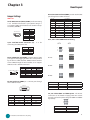
Icon Descriptions
The icons are used in the manual to serve as an indication
of interest topics or important messages. Below is a
description of these icons:
NOTE: This check mark indicates that
there is a note of interest and is something
that you should pay special attention to
while using the product.
WARNING: This exclamation point
indicates that there is a caution or
warning and it is something that could
damage your property or product.
Intel, Pentium and Celeron are registered trademarks of
Intel Corp.
Microsoft Windows and MS-DOS are registered trademarks
of Microsoft Corp.
All other product names or trademarks are properties of
their respective owners.
Compliances and Certification
CE Certification
This product has passed the CE test for environmental
specifications. Test conditions for passing included the
equipment being operated within an industrial enclosure.
In order to protect the product from being damaged by
ESD (Electrostatic Discharge) and EMI leakage, we strongly
recommend the use of CE-compliant industrial enclosure
products.
FCC Class A Certification
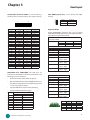
Online Resources
The listed websites are links to the on-line product
information and technical support.
Resource
Website
Lanner
http://www.lannerinc.com
Product Resources http://assist.lannerinc.com
RMA
This equipment has been tested and found to comply
with the limits for a Class A digital device, pursuant to Part
15 of the FCC Rules. These limits are designed to provide
reasonable protection against harmful interference when
the equipment is operated in a commercial environment.
This equipment generates, uses and can radiate radio
frequency energy and, if not installed and used in
accordance with the instruction manual, may cause
harmful interference to radio communications. Operation
of this equipment in a residential area is likely to cause
harmful interference in which case the user will be required
to correct the interference at his own expense.
http://eRMA.lannerinc.com
Copyright and Trademarks
This document is copyrighted, © 2011. All rights are
reserved. The original manufacturer reserves the right to
make improvements to the products described in this
manual at any time without notice.
No part of this manual may be reproduced, copied,
translated or transmitted in any form or by any means
without the prior written permission of the original
manufacturer. Information provided in this manual is
intended to be accurate and reliable. However, the original
manufacturer assumes no responsibility for its use, nor for
any infringements upon the rights of third parties that
may result from such use.
Embedded and Industrial Computing
2
TTaTTable of Contentsbeable of Conten
Chapter 1: Introduction
4
System Specification . . . . . . . . . . . . . . . . . . . . . . . . . . . . . . . . . . . . . . . . . . . . 4
Package Contents . . . . . . . . . . . . . . . . . . . . . . . . . . . . . . . . . . . . . . . . . . . . . . 5
Chapter 2: System Components
6
System Drawing . . . . . . . . . . . . . . . . . . . . . . . . . . . . . . . . . . . . . . . . . . . . . . . 6
Block Diagram . . . . . . . . . . . . . . . . . . . . . . . . . . . . . . . . . . . . . . . . . . . . . . . . 7
Front Components . . . . . . . . . . . . . . . . . . . . . . . . . . . . . . . . . . . . . . . . . . . . . 8
Rear Components . . . . . . . . . . . . . . . . . . . . . . . . . . . . . . . . . . . . . . . . . . . . . . 9
Chapter 3: Board Layout
10
External Connectors . . . . . . . . . . . . . . . . . . . . . . . . . . . . . . . . . . . . . . . . . . . 10
Internal Connectors and Jumpers . . . . . . . . . . . . . . . . . . . . . . . . . . . . . . . . . . . 11
Connectors and Jumpers List . . . . . . . . . . . . . . . . . . . . . . . . . . . . . . . . . . . . . 12
Jumper Settings . . . . . . . . . . . . . . . . . . . . . . . . . . . . . . . . . . . . . . . . . . . . . . 13
Chapter 4: Hardware Setup
18
Preparing the Hardware Installation . . . . . . . . . . . . . . . . . . . . . . . . . . . . . . . . . 18
Installing the System Memory . . . . . . . . . . . . . . . . . . . . . . . . . . . . . . . . . . . . . 18
Installing the Hard Disk . . . . . . . . . . . . . . . . . . . . . . . . . . . . . . . . . . . . . . . . . 18
Installing a CompactFlash Card . . . . . . . . . . . . . . . . . . . . . . . . . . . . . . . . . . . . 19
3G SIM Card Installation . . . . . . . . . . . . . . . . . . . . . . . . . . . . . . . . . . . . . . . . . 19
Wireless 3G module Installation . . . . . . . . . . . . . . . . . . . . . . . . . . . . . . . . . . . . 19
Wall Mounting . . . . . . . . . . . . . . . . . . . . . . . . . . . . . . . . . . . . . . . . . . . . . . . 20
Appendix A: Programming Watchdog Timer
21
Appendix B: Digital Input/Output Control on the GPIO port
30
Appendix C: Terms and Conditions
36
Warranty Policy . . . . . . . . . . . . . . . . . . . . . . . . . . . . . . . . . . . . . . . . . . . 36
RMA Service . . . . . . . . . . . . . . . . . . . . . . . . . . . . . . . . . . . . . . . . . . . . . 36
3
Chapter 1
Chapter 1:
Introduction
Thank you for choosing the LEC-7105. The LEC-7105 is
Lanner’s flagship IPC. It features the Dual Core Intel®
Atom™ D525 processor that has 1.8GHz of processing
power.
The LEC-7105 is an ideal solution for digital signage and
public infortainment. All electronics are protected in a
compact sealed aluminum case as a stand-alone unit and
can be easily situated in a place where space is limited and
the weather condition is diverse.
A solid sealed Aluminum extrusion framing provides
vibration and dust resistance while providing a passive
cooling solution. It also provides great protection from
EMI and shock.
Introduction
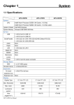
System Specification
LEC 7 Series
Dimension (WxHxD)
268x44x174mm
(10.55”x1.73”x6.85”)
Processor
Intel Atom D525 1.8GHz
Chipset
System
Memory
Storage
Audio
Serial I/O
IO
GPS
Digital I/O
USB 2.0
Power Input
with a SIM card reader that can support 3G Internet
and the other Mini-PCIe can support Wi-Fi or Bluetooth
connection)
Expansion
Others
•• One power eSATA (5V external SATA) which also
232/422/485 selectable, and Digital Input/Output
(through 2 x 5-pin terminal block)
2.5” HDD/SSD drive bay x1
Video Grabber
•• Two Mini-PCIe expansion slots (One Mini-PCIe comes
•• USB x 4, COM x 2 (COM1 is RS-232 and COM2 is RS-
SATA
Display
which supports VGA (up to 2048x1536) and DVI-D
(1920 x1080)
supports USB connectivity. The Power eSATA solution
incorporates the eSATA connector with power source
together, allowing you to use external SATA devices
without the need of additional power source. It
provides storage for photos, videos and other multimedia contents.
Intel ICH8M
DDR3 SODIMM x1
Up to 4GB
CF socket Type I/II x1
LAN
•• Intel integrated Graphics Media Accelerator 3150
LAN) and Remote-wake-up)
Technology
Max. Capacity
IDE
Ethernet Controller
Graphic Controller
Audio Controller
Here is the list of the key features:
•• Dual 10/100/1000 Mbps LAN (support WOL (Wake-on-
LEC-7105
Power Input
AC Adapter
Hardware Monitor
OS Support
Certifications
Compliance
Operating Temperature Range
with
Commercial Components
Realtek RTL8111 x2
Intel GMA3150
Realtek ALC888S
GbE RJ45 x2
DB15 x1 for VGA, DVI-D
( up to1920x1080)
No
RCA x2 for right/left Line-out
channels, Internal pin header for
Line-out, Line-in and Mic-in
DB9 x2 for RS232 x1;
RS232/422/485 x1
No
2 x 5-pin terminal block for DI x4
and DO x4 (5V TTL)
Type A x4; Internal x2
DC jack with lock
Mini-PCIe x2 (one with SIM card
reader)
External: Power-on button,
Power-on switch, 3x SMA
antenna hole, reset.
Internal: PS/2 keyboard and
mouse, +5Vdc output
+12Vdc +/- 5%, ATX mode
60W +12V @ 5A
Winbond W83627UHG integrated watchdog timer 1~255
level
Linux , XPE/WES2009, XP PRO
FES, WS7E, WS7P, WIN 7 PRO-E
CE, FCC Class A
No
-5~45°C/23~113°F
•• Audio output for L/R channels with RCA connectors (
Realtek ALC888S codec)
Embedded and Industrial Computing
4
Chapter 1
Introduction
Package Contents
Your package contains the following items:
•• LEC-7105 Embedded System
•• DC+12V 60W Power Adapter (080W240318306, US
type)
•• Serial-ATA/Power Cable (P/N: 080W1N2201001)
•• Wall-Mounting Kit (P/N: SE9ESA900R100)
•• Drivers and User’s Manual CD
Embedded and Industrial Computing
5
Chapter 2
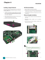
System Components
Chapter 2:
System Components
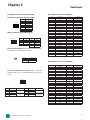
System Drawing
Mechanical dimensions of the LEC-7105
Unit: mm
Embedded and Industrial Computing
6
Chapter 2
System Components
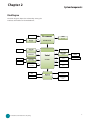
Block Diagram
The block diagram depicts the relationships among the
interfaces and modules on the motherboard..
VGA
DVI
LVDS to DVI
Encoder
VGA
Processor
DDR3
SO-DIMM
LVDS
CH7036
ATOM D525
DMI
2x RJ-45
MIC/Line In
2x PCIe
SATA
BIOS Flash
SPI
PCIe
USB
HD Audio
HD
GbE LAN
2x RTL8111
Reaktek ALC888S
Aduio/Line Out
USB 2.0 Ports
4x Type A
1x Pin Header
Intel
ICH8M
USB
PCIe
USB
SATA-II
2x Connector
PCIe to SATA
Controller
JMB362
Mini PCI Express
Socket
Power
eSATA
SIM Card Reader
Mini PCI Express
PCIe
SATA
Socket (Support mSATA)
IDE
Compact Flash
Socket
LPC
H/W Monitor
WDT
PS/2 KB/MS
Pin Header
Embedded and Industrial Computing
Digital IO
Winbond
W83627UHG
Terminal Block
Serial Port
RS232
RS232/422/485
2x DB-9
7
Chapter 2
System Components
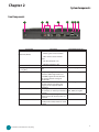
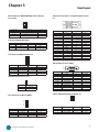
Front Components
Component
F4
F3
F2
F1
Description
F1 HDD (Yellow) and
HDD
Power Led (Green)
•
Blinking: data access activities
•
Off: no data access activities
F5
F6
F7
F8
Pin Definition Reference
Power
•
F2 Antenna Hole
F3 Line_Out_R
Line_Out_L
F4 Serial Ports 1 and 2
F5 Power eSATA
F6 Dual USB Stack Connector
F7 Power-on Switch
F8 Power Button with dual LED
Embedded and Industrial Computing
On: The computer is on.
• Off: The computer is off .
Reserved for antenna
RCA Jack for audio output left and
right
CN1, CN2 on page 17
Serial ports through the DB-9
COM1, COM2 on page 14
connector; COM1 supports RS-232
and COM2 supports RS-232/422/485
with switch selection among RS232/422/485.
An external SATA connector with
EUSB1 on page 14
5V power supply and support hot
plugging. It also supports USB 2.0
connection.
An USB type A connector; in addition to Dual USB Port Connectors
this connector, an internal pin header is (USB1, USB2) on Page16
provided.
A power-on switch through the
J12 on page 16
Phoenix contact for distant power-on/
off control
ATX Power-on button with LEDs:
Standby mode in Red; Power-on mode
in Green
8
Chapter 2
System Components
Rear Components
R1
Component
R1 Antenna Hole
R2 VGA Port
R2
R3
R4
R5
Description
R6
R7
Pin Definition Reference
Reserved for antenna
DB-15 Female Connector for VGA VGA1 on page 17
connection (up to 2048x1536)
R3 DVI-D
DVI-D port (single link) is provided
by Intel GMA 3150 through the
Chrontel’s CH7036 LVDS to DVI
converter.
R4 DIO Port
4 digital input and 4 output ports
to support input and output
operations.
R5 Dual USB Stack Connector An USB type A connector; in
addition to this connector, an
internal pin header is provided.
R6 Dual 10/100/1000 LAN
Two RJ-45 (network) jacks with LED
Ports
indicators as described below. The
speed
LINK/ACT
LAN ports are provided by Realtek
RTL8111. They both support WOL
(Wake-on-LAN) and Remote-wakeup.
DVI1 Connector on page 17
DIO1 on page 15
Dual USB Port Connectors (USB1,
USB2) on Page 16
LAN Ports (LAN1/LAN2) on page
15
LINK/ACT (Yellow)
•
On/Flashing: The port is linking
and active in data transmission.
•
Off: The port is not linking.
SPEED (Green/Amber)
•
Amber: The connection speed is
1000Mbps.
•
Green: The connection speed is
100Mbps
•
R7 DC Jack
Embedded and Industrial Computing
Off: .The connection speed is
10Mbps.
DC-in 12V power socket with
Lock. Only use the power adapter
supplied with the LEC-7105 System.
9
Chapter 3
Board Layout
Chapter 3:
Board Layout
External Connectors
The following picture highlights the location of system
input/output connectors. Refer to the table 3.1 Connector
List for more details.
CN7
LAN1/LAN2
USB1
DIO1
RST1
DVI1
VGA1
EUSB1
CN2/CN1
Embedded and Industrial Computing
USB2 J12 BUT1
COM2/COM1
10
Chapter 3
Board Layout
Internal Connectors and Jumpers
The following picture highlights the location of internal
connectors and jumpers. Refer to the table 3.1 Connector
List for more details.
J3
J1
J13
SATA2
SATA1
J27
J6
CN8
J7
J25
KBM1
CFD1
J2
SCT2 SCT1
JP1
JP2
JP3 J10
J11
LPC1
LEB-7105
Embedded and Industrial Computing
11
Chapter 3
Board Layout
Connectors and Jumpers List
The tables below list the function of each of the board
jumpers and connectors by labels shown in the above
section. The next section in this chapter gives pin
definitions and instructions on setting jumpers.
Table 3.1 Connector List for LEB-7105
Labels
Function
CFD1
CN1 & CN2
COM1
COM2
DIO1
DVI1
EUSB1
J1
J10
J11
J12
J13
J2
J25
J27
J3
J6
J7
JP1 & JP2
JP3
KBM1
LAN1/LAN2 Ports
LPC1
MPCIE1
MPCIE2
SATA1
SATA2
SCT1/SCT2
USB1
USB2
VGA
CompactFlash
Lineout Left/Right
RS-232 Port
RS-232/422/485 Port
Digital Input/Output
DVI-D Connector
Power eSATA Port
SPI ROM Header
USB Pin Header
Miscellaneous Front Panel Pins
External Power Switch
SYSTEM Thermal Sensor
Line In/Out and MIC Pin Header
Mini-PCIe Power Voltage Selection
Power for Passive Antenna
SATA Power
ICH8M Chipset SMB Signals
LAN and WLAN LED (Only on MPCIE1)
Select COM1/COM2 Pin9 Function Jumper Settings
Clean CMOS
PS/2 Keyboard and Mouse
LAN1, LAN2 ports
Low Pin Count Bus for Debug Purpose
Mini-PCIe Slot (with SIM Card Reader)
Mini-PCIe Slot
Serial-ATA Connector 1
Serial-ATA Connector 2
Seclect COM2 Protocol Jumper settings
Dual USB Port
Dual USB Port
DB-15 VGA Port
Embedded and Industrial Computing
Pin Definition Reference
Page
P15
P17
P14
P14
P15
P17
P14
Reserved for Factory
P16
P16
P16
P17
P17
P17
P18
P14
Reserved for Factory
P17
P14
P15
P17
P15
Reserved for Factory
P16
P16
P14
P14
P14
P16
P16
P17
12
Chapter 3
Board Layout
RS-232/422/485 Serial Port(COM2): It is a RS-232/422/485
port through the D-SUB9 connector.
Jumper Settings
LEB-7105
Pin No.
Serial-ATA Connector (SATA1, SATA2): It is for connecting
a 2.5’’ harddisk to be served as your system’s storage. It
can support SATA II which features Data transfer rates up
to 3.0 Gb/s (300 MB/s).
Pin No.
1
2
3
4
5
6
7
1234567
Function
GND
TX0_+
TX0_GND
RX0_RX0_+
GND
4321
It is for
S7 S6 S5 S4 S3 S2 S1
Function
GND
TX1_+
TX1_GND
RX1_RX1_+
VCC5
1
3
5
Pin No.
1
2
3
4
SCT1
SCT2
Function
+5V
GND
GND
+12V
Power eSATA Port (5V, EUSB1): A Power external SATA
port supports hot plugging of SATA II disc. It was provided
by the PCIe to SATA controller: JMB362 which connects
to the ICH8M through the PCIe interface. It can support
USB2.0 as well as eSATA transmission.
Pin No.
1
2
3
4
5
6
7
RS-485
DataData+
SCT1, SCT2: Select COM2 Protocol Setting
4-pin Serial-ATA Power Connector (J3):
connecting the SATA power cord.
Pin No.
1
2
3
4
1
2
3
4
5
6
7
8
9
Pin Name
RS-422
TxDTxD+
RxDRxD+
RS-232
DCD
RXD
TXD
DTR
GND
DSR
RTS
CTS
RI
9
5
1
2
4
6
12
8
4
RS-232
RS-422
Function
+5V
USB8+
USB8GND
RS-485
RS-232 Serial Port (COM1): It is a RS-232 port through
the D-SUB9 connector.
12345
COM1 TYPE
RS-232 (Default)
RS-422
RS-485
SCT2
1-2
3-4
5-6
SCT1
1-5, 2-6, 3-7, 4-8
5-9, 6-10, 7-11, 8-12
5-9,6-10,7-11,8-12
6789
Pin No.
1
2
3
4
5
Pin Name
DCD
RXD
TXD
DTR
GND
Pin No.
6
7
8
9
Pin Name
DSR
RTS
CTS
RIA
JP1, JP2: Select COM1 and COM2 power : The Pin No.
9 of RS-232 can be altered to supply power. JP1 and JP2
are used to select the power voltage for COM1 and COM2
respectively.
6
4
2
RS-232 Pin 9 Function
+5V
+12V
RI (Default)
Embedded and Industrial Computing
5
3
1
JP1, JP2
1-2
3-4
5-6
13
Chapter 3
Board Layout
CompactFlash Connector (CFD1): It is for connecting a
Compact Flash card to be served as your system’s storage.
Pin No.
Pin
1
2
3
4
5
6
7
8
9
10
11
12
13
14
15
16
17
18
19
20
21
22
23
24
25
50
26
25
1
Function
Signal
GND
PDD3
PDD4
PDD5
PDD6
PDD7
PDCS1_N
GND
GND
GND
GND
1GND
VCC5
GND
GND
GND
GND
PDA2
PDA1
PDA0
PDD0
PDD1
PDD2
IOCS16#
CD2#
Pin No.
Pin
26
27
28
29
30
31
32
33
34
35
36
37
38
39
40
41
42
43
44
45
46
47
48
49
50
1
2
3
Function
Signal
CD1#
PDD11
PDD12
PDD13
PDD14
PDD15
PDCS3_N
N/A
PDIOR_N
PDIOW_N
WE#
IRQ14
VCC5
CSEL#
N/A
PRST
PDIORDY
PDDREQ
PDDACK
PDACTIVE
PATADET
PDD8
PDD9
PDD10
GND
LAN1/LAN2 Ports (LAN1/LAN2): The LAN ports are
provided by Realtek RTL8111E Ethernet Controllers. The
following lists its main features:
•
Wake-on-LAN and remote wake-up support
•
Microsoft NDIS5, NDIS6 Checksum Offload (IPv4, IPv6,
TCP, UDP) and Segmentation Task-offload (Large send
v1 and Large send v2) support
•
Supports IEEE 802.1P Layer 2 Priority Encoding
• Supports IEEE 802.1Q VLAN tagging
Pin No. Description
Fast Ethernet Gigabit Ethernet
1
TX+
BI_DA+
2
TXBI_DA3
RX+
BI_DB+
4
-BI_DC+
5
-BI_DC6
RXBI_DB7
-BI_DD+
8
-BI_DD-
Embedded and Industrial Computing
Clear CMOS jumper (JP3): It is for clearing the CMOS
memory.
Pin No.
1-2
2-3
Pin Name
Normal (Default)
Clear CMOS
Digital I/O (DIO1)
Digital IN/OUT(DIO1) Connector: The 8 pins of digital
Input/Output (GPIO) support input and output operations
through the 2x5-pin terminal block.
TTL Level is +5V; Maximum input/output current for
each port is 20mA
Input/Output Voltage
Logic
Register
0~2V
Low
0
2~5V
High
1
The output default value is 0
DIO Address LDN8
Address
Description
0x2e
SUPERIO_INDEX
0x2f
SUPERIO_DATA
0x07
BANK_REG
0xE6 (Bit 3)
GPO63
0: Low 1: High
0xE6 (Bit 2)
GPO62
0: Low 1: High
0xE6 (Bit 1)
GPO61
0: Low 1: High
0xE6 (Bit 0)
GPO60
0: Low 1: High
DIO Address LDN9
Address
Description
0x2e
SUPERIO_INDEX
0x2f
SUPERIO_DATA
0x07
BANK_REG
0xE6 (Bit 3)
GPI24
0: Low 1: High
0xE6 (Bit 2)
GPI25
0: Low 1: High
0xE6 (Bit 1)
GPI26
0: Low 1: High
0xE6 (Bit 0)
GPI27
0: Low 1:High
1 3 5 7 9
2 4 6 8 10
Pin No. Pin Name Pin No. Pin Name
2
Output0
1
Input0
4
Output1
3
Input1
6
Output2
5
Input2
8
Output3
7
Input3
10
GND
9
GND
14
Chapter 3
Board Layout
Dual USB Port Connector #0 and #1 (USB1):
Dual USB Port Connector #2 and #3 (USB2)
5 6 7 8
1 2 3 4
Pin No.
1
2
3
4
5
6
7
8
Pin Name
+5V
USBD1USBD1+
GND
+5V
USBD0USBD0+
GND
USB 2.0 Pin Header (J10, USB#4 and #5):
2 4 6 8 10
13579
Pin No.
1
3
5
7
Pin Name
+5V
USBD4USBD4+
Ground
Pin No.
2
4
6
8
10
Pin Name
+5V
USBD5USBD5+
Ground
NC
External Power Button (J12): The external power button
is provided for distant power-on control.
PIN NO.
1
2
12
DESCRIPTION
PWR_BTN_N
GND
Front Panel Function Pin Header (J11): It provides
redundant LED signal and button function on the front
panel.
7531
8642
Pin No.
Pin Name
1
POWER_LED
3
HD_LED
5
Reset
7
GND
Function
HDD LED
Pin No.
Pin Name
Function
2
PWR_LED+
Power LED
4
GND
System Reset
6
POWER_BTN- Power On/Off
8
GND
Button
Push Button
Embedded and Industrial Computing
Mini PCI Express Connector 1(MPCIE1):
PIN
1
3
5
7
9
11
13
15
17
19
21
23
25
27
29
31
33
35
37
39
41
43
45
47
49
51
Pin Name
WAKE#
N/A
N/A
CLKREQ#
GND
CLK_PCIE_MINI_N1
CLK_PCIE_MINI_P1
GND
RSV
RSV
GND
PCIE_RX_N2
PCIE_RX_P2
GND
GND
PCIE_TX_N2
PCIE_TX_P2
GND
GND
VCC3.3
VCC3.3
GND
RSV
RSV
RSV
RSV
PIN
2
4
6
8
10
12
14
16
18
20
22
24
26
28
30
32
34
36
38
40
42
44
46
48
50
52
Pin Name
VCC3.3
GND
VCC1.5
VREG_USIM
UIM_DATA
UIM_CLK
UIM_RESET
UIM_VPP
GND
RF_KILL_N1
PLTRST
PCIE1_P24
GND
VCC1.5
SMBCLK
SMBDATA
GND
USB_N6
USB_P6
GND
LED1_WWAN
LED1_WLAN
LED1_WPAN
VCC1.5
GND
VCC3.3
Mini PCI Express Connector 2 (MPCIE2)
PIN
1
3
5
7
9
11
13
15
17
19
21
23
25
27
29
31
33
35
37
39
41
43
45
47
49
51
Pin Name
WAKE#
N/A
N/A
CLKREQ#
GND
CLK_PCIE_MINI_N2
CLK_PCIE_MINI_P2
GND
RSV
RSV
GND
PCIE_RX_N4
PCIE_RX_P4
GND
GND
PCIE_TX_N4
PCIE_TX_P4
GND
GND
VCC3.3
VCC3.3
GND
RSV
RSV
RSV
RSV
PIN
2
4
6
8
10
12
14
16
18
20
22
24
26
28
30
32
34
36
38
40
42
44
46
48
50
52
Pin Name
VCC3.3
GND
VCC1.5
N/A
N/A
N/A
N/A
N/A
GND
RF_KILL_N2
PLTRST
PCIE2_P24
GND
VCC1.5
SMBCLK
SMBDATA
GND
USB_N7
USB_P7
GND
N/A
N/A
N/A
VCC1.5
GND
VCC3.3
15
Chapter 3
Board Layout
Mini PCI Express (MPCIE1/MPCIE2) Power Setting in
Pin 24 (J25):
7
5
3
1
8
6
4
2
Connector
MPCIE1
MPCIE1
MPCIE2
MPCIE2
Description
+3.3V Standby (miniPCIe 1.2)
+3.3V Default (miniPCIe 1.0)
+3.3V Standby (miniPCIe 1.2)
+3.3V Default (miniPCIe 1.0)
J25
1-2
5-6
3-4
7-8
Line Out Left/Right (CN1/CN2)
Pin No.
1
2
CN1
Description
GND
FRONT_OUT_L
Pin No.
1
2
CN2
Description
GND
FRONT_OUT_R
Line In/Out and MIC Pin Header (J2)
1
3
5
7
9
Pin No.
1
3
5
7
9
2
4
6
8
10
Description
LINE_OUT2_R
GND
MIC_R
LINE_IN_R
LINE_IN_L
Description
LINE_PUT2_L
GND
MIC_L
N/A
GND
2
1
Pin No.
1
2
Description
SYS_TIN
GND
Description
+5V
MDATA
KDATA
GND
Description
Pin No.
Description
Pin No.
Description
Pin No.
Description
1
2
3
4
5
6
7
8
17
18
19
20
21
22
23
24
TXD_2TXD_2+
GND
N/A
N/A
DDC_CLK
DDC_DATA
9
10
11
12
13
14
15
16
TXD_0TXD_0+
GND
NC
NC
GND
TXD_CLK_P
TXD_CLK_N
C1
C2
C3
C4
C5
C6
TXD_1TXD_1+
GND
N/A
N/A
VCC5
GND
HPD
GND
GND
Pin No.
1
2
3
4
5
Pin No.
11
12
13
14
15
Embedded and Industrial Computing
Description
RED
GREEN
BLUE
N/A
GND
Description
N/A
DDC DAT
HSYNC
VSYNC
DDC CLK
6
4
2
7
5
3
1
Pin No.
2
4
6
8
1
6
11
5
10
15
Pin No.
6
7
8
9
10
Description
CRT DET
GND
GND
VCC5
GND
LAN and WLAN LED (Only on MPCIE1, J7)
PS/2 Keyboard and Mouse (KBM1)
8
6
4
2
Pin No.
DB-15 VGA Connector (VGA1)
Pin No.
2
4
6
8
10
SYSTEM Thermal Sensor ( J13)
Pin No.
1
3
5
7
DVI-D Connector (DVI1): A single link DVI-D connector
Description
MCLK
NC
NC
KCLK
Pin No.
1
3
5
Description
LED1_WWAN
LED1_WLAN
LED1_WPAN
5
3
1
Pin No.
2
4
6
Description
+3.3V
+3.3V
+3.3V
16
Chapter 3
Board Layout
Power for Passive Antenna (J27)
12
Pin No.
1
2
Description
+3.3V
GND
Embedded and Industrial Computing
17
Chapter 4
Chapter 4:
Hardware Setup
Introduction
Note:
1. The
motherboards can support up to 4 GB
memory capacity in maximum.
Preparing the Hardware Installation
Installing the Hard Disk
To access some components and perform certain service
procedures, you must perform the following procedures
first.
The system can accomdate two Serial-ATA disks. Follow
these steps to install a hard disk into the LEC-7105:
WARNING: To reduce the risk of personal injury,
electric shock, or damage to the equipment,
remove the power cord to remove power from the
server. The front panel Power On/Standby button
does not completely shut off system power.
Portions of the power supply and some internal
circuitry remain active until AC power is removed.
1. Unpower the LEC-7105 and remove the power cord.
2. Unscrew the 3 threaded screws on both sides of the
top cover of the LEC-7105 System.
3. Slide the cover backwards and open the cover
1. Unsrew the 4 screws on the hard disk tray to take out
the hard disk tray from the system.
2. Place hard disk on the hard disk tray and align the holes
of the hard disk with the mounting holes on the tray.
3. Secure the hard disk with 4 mounting screws on the
hard disk tray.
4. Connect the Serial-ATA power and datacables to the
hard disk’s connectors respectively.
5. Plug the Serial-ATA cable to the Serial-ATA Connector
on the main board.
6. Put the hard disk tray with the installed hard disk back
to the system and secure it with the mounting screws.
upwards.
1
Installing the System Memory
The motherboard supports DDR3 memory. It comes with
one Double Data Rate (DDR3) Small Outline Dual Inline
Memory Modules (SO-DIMM) sockets.
2
1. Open the SO-DIMM slot latches.
2. Install the SO-DIMM.
Embedded and Industrial Computing
18
Chapter 4
Introduction
Installing a CompactFlash Card
3G SIM Card Installation
LEC-7105 provides one CompactFlash slot. To install the
CF card, Follow these procedures bellow for installing a
CompactFlash card.
1. Open the SIM tray and flip it diagnolly.
1. In order to insert the CF card, you will have to take off
the front panel first. To take off the front panel, unscrew
the 2 screws on the front panel and the hex-shaped
screws of the COM ports.
2. Align CompactFlash card and the card slot with the
arrow pointing toward the connector.
3. Push the card to insert into the connector.
1
2. Align the cut corner of the SIM card with the SIM card
socket. Make sure the ICs is in contact with the reader.
3. Insert the SIM card into the tray diagonally. Close and
lock the tray.
Wireless 3G module Installation
1. Align the wireless module’s cutout with the Mini-PCIe
slot notch.
2. Insert the wireless module into the connector
diagnoally.
3. Push the other end of the wireless module to be
tightened with the latch.
3
3G module
1
2
SIM Card
2
3
2
Note:
1. To remove the module from the system, release
2.
lock
Embedded and Industrial Computing
the latch first by slightly bending it inward.
To remove the SIM card, unlock the tray first by
sliding it outward.
Unlock
19
Chapter 4
Introduction
Wall Mounting
The product ships with wall mounting kit. To mount your
product on the wall, follow the instructions below:
1. First make a hole for the anchor in the surface on the
wall.
2. Then press the anchor into the hole until it is flush with
the surface. You may need a hammer to tap the wall
anchor.
3. Use a screwdriver to screw the threaded screw into the
plastic anchor.
4. Attach the wall mounting bracket to the back of the
device, securing it in place with four of the flat-head
screws provided.
5. Hang the device on the wall.
Unit: mm
Embedded and Industrial Computing
20
Appendix A
Appendix A:
Programming Watchdog
Timer
A watchdog timer is a piece of hardware that can be used
to automatically detect system anomalies and reset the
system (or one pair of network ports in bypassed state;
However, only one function can be activated at a time.)
in case there are any problems. Generally speaking, a
watchdog timer is based on a counter that counts down
from an initial value to zero. The software selects the
counter’s initial value and periodically restarts it. Should
the counter reach zero before the software restarts it,
the software is presumed to be malfunctioning and the
processor’s reset signal is asserted. Thus, the processor
will be restarted as if a human operator had cycled the
power.
For sample watchdog code, see wd_bp folder under Driver
and Utility on the Driver and Manual CD
Programming Watchdog Timer
2. Set the access mode with these two parameters
by editing the Makefile.linux directly: DIRECT_IO_
ACCESS= [0|1] (enter either 1 or 0) and LANNER_
DRIVER= [0|1] (enter either 1 or 0). 1 is for direct access
and no driver is needed. You will only need to execute
the program directly. However, when it equaled to 0,
driver installation is needed. Refer to the following
Install section for more details.
3. Type make to build source code:
make Makefile (Note: omit the file extensions)
After compiled, the executable program (bpwd_tst) and
the driver (bpwd_drv.ko) will be in the bin subdirectory.
Install
The installation procedures depend on the access mode
that you have set by using the above mentioned method.
If you have set DIRECT_IO_ACCESS=1, driver installation is
not necessary. Proceed to the next section on executing
If you have set DIRECT_IO_ACCESS=0, Lanner bypass
driver needs to be installed. Install the driver and create
a node in the /dev directory as shown in the following
example:
For Linux:
Executing the commands through the Command Line:
1. wd_tst --swtsr (Set Watchdog Timeout State to Reset)
2. wd_tst --swt xxx (Set Watchdog Timer 1-255 seconds)
3. wd_tst[*] --start (Start Watchdog Timer)
4. wd_tst --stop (Stop Watchdog Timer)
The following procedures are required for running the
watchdog program on DOS, Linux and FreeBSD.
Note:
1. For DOS environment, use DJGPP as compiler
and the makefile: Makefile.dos.
2. For Linux, support kernel versions are 2.4.x and
2.6.x. Use the makefile:Makefile.linux.
3. For FreeBSD, support version is FreeBSD 8.0.
Use the makefile: Makefile.
Insert module and create node in /dev as below
example:
#insmod wd_drv.[k]o
#mknod /dev/wd_drv c 241 0
For FreeBSD:
Insert module as below example:
#kldload -v ./wd_drv.ko
Execute
# wd_tst --swtsb (Set Watchdog Timeout State to Bypass
function)
# wd_tst --swtsr (Set Watchdog Timeout State to Reset
function)
# wd_tst --swt xxx (Set Watchdog Timer 1-255 seconds)
Build
# wd_tst[*] --start (Start Watchdog Timer)
To build program source code on Linux platform, use the
following steps as a guideline:
# wd_tst --stop (Stop Watchdog Timer)
Note:
1. Copy the proper makefile from the Driver and Manual
CD to your system
Embedded and Industrial Computing
1.
wd_tst --start will not be available if
21
Appendix A
2.
3.
DIRECT_IO_ACCESS=1, use the command: “./
wd_tst --swt xxx” to start the watchdog timer
instead .
Watchdog timer can support two functions,
- system rest or LAN bypass. However, only
one function can be activated at a time. You
should modify the code or switch it to the
desired state/function accordingly.
For more details, refer to the README file
contained within the program.
Programming Watchdog Timer
#if defined(FreeBSD_ENV)
#include <machine/cpufunc.h>
#endif
#include <time.h>
#include <stdint.h>
#include <fcntl.h>
A sample Watchdog program in C:
#include <errno.h>
#include <string.h>
*********************************************************
**********************/
#define delay(x) usleep(x)
#endif
#include “../include/config.h”
#ifdef MODULE
#ifdef DJGPP
#include <linux/kernel.h>
/* standard include file */
#include <linux/module.h>
#include <stdio.h>
#include <linux/kernel.h>
#include <stdlib.h>
#include <linux/fs.h>
#include <unistd.h>
#include <asm/io.h>
/* For DOS DJGPP */
#include <linux/delay.h>
#include <dos.h>
#include <inlines/pc.h>
#undef delay
#define delay(x) mdelay(x)
#else //DJGPP
#undef fprintf
/* For Linux */
#define fprintf(S, A) printk(A)
#endif //MODULE
#ifdef DIRECT_IO_ACCESS
/* For Linux direct io access code */
#ifdef KLD_MODULE
/* standard include file */
#include <stdio.h>
#include <sys/types.h>
#include <stdlib.h>
#include <sys/param.h>
#include <unistd.h>
#include <sys/systm.h>
#include <sys/malloc.h>
#if defined(LINUX_ENV)
#include <sys/kernel.h>
#include <sys/io.h>
#include <sys/bus.h>
#endif
Embedded and Industrial Computing
22
Appendix A
#include <sys/errno.h>
Programming Watchdog Timer
*
1
GPO23=0
Enable
GPO22=1
*
1
GPO23=1
Disable
GPO22=0
*
2
GPO31=0
Enable
GPO30=1
#endif
*
2
GPO31=1
Disable
GPO30=0
#endif
*
#include <machine/bus.h>
#include <machine/resource.h>
* Runtime:
/* local include file */
* ========
#include “../include/ioaccess.h”
* It is able to set Lan bypass enable/disable alone, or design
hybrid with
#if (defined(MODULE) || defined(DIRECT_IO_ACCESS) ||
defined(KLD_MODULE))
* watchdog timeout(WDTO#).
* The IO interface for this function is conjunction with
Winbond 83627
* GPO24 (Pair1), GPO60(Pair2) and WDTO#.
* Refer to Winbond 83627 datasheet for details.
/*
* Platform Depend GPIOs Interface for Watchdog and Lan
bypass
* The truth table is defined as below:
*
* Below setting is to determine system behavior while
watchdog timer expired.
*/
/*
*-----------------------------------------------------------------------------
*
*
GPO27 System behavior
* LEB-7105 Version V1.0
* ------------------------------------------------
*
* 0
* LEB-7105 embedded with HW Watchdog timer functions.
* 1 * Set Lan bypass Enable/Disable while System-off:
*
* ======================================
=========
* Below setting is to determine lan bypass in runtime mode
* It is able to set Lan bypass enable/disable in system off
mode by SW program.
*
* The IO interface for off-mode bypass is connected to
Winbond SIO 83627UHG
*
1
Enable
GPO24 =1
*
1
Disable
GPO24 =0
*
2
Enable
GPO60 =1
*
2
Disable
GPO60 =0
* GPO22,GPO23(Pair1), GPO30,GPO31(Pair2),
* Refer to Winbond 83527 datasheet for details.
*
* The truth table of function is defined as below:
*
*
*
Pair Bypass function GPIO Pin
--------------------------------------------------Embedded and Industrial Computing
Lan-bypass while watchdog timeout
System Reset while watchdog timeout
*
*
Pair
Bypass function GPIO Pin
-----------------------------------------------------------
*
*
Note: To sete runtime bypass mode, user need to set
off-mode bypass
*
enabled in order to let function activity.
*
23
Appendix A
*-----------------------------------------------------------------------------
Programming Watchdog Timer
{
unsigned char tmp = 0;
enter_w83627_config();
outportb(INDEX_PORT, 0x07); // LDN Register
*-----------------------------------------------------------------------------
outportb(DATA_PORT, LDN); // Select LDNx
outportb(INDEX_PORT, reg); // Select Register
*/
tmp = inportb( DATA_PORT ); // Read Register
/*
exit_w83627_config();
* Device Depend Definition : Winbond 83627UHG
*/
return tmp;
}
#define INDEX_PORT
0x2E
#define DATA_PORT
0x2F
#define SIO_GPIO_22_BIT 0x04
#define SIO_GPIO_23_BIT 0x08
void write_w83627_reg(int LDN, int reg, int value)
{
enter_w83627_config();
#define SIO_GPIO_24_BIT 0x10
outportb(INDEX_PORT, 0x07); // LDN Register
#define SIO_GPIO_27_BIT 0x80
outportb(DATA_PORT, LDN); // Select LDNx
#define SIO_GPIO_30_BIT 0x01
outportb(INDEX_PORT, reg); // Select Register
#define SIO_GPIO_31_BIT 0x02
outportb(DATA_PORT, value); // Write Register
#define SIO_GPIO_60_BIT 0x01
exit_w83627_config();
return;
void enter_w83627_config(void)
}
{
outportb(INDEX_PORT, 0x87); // Must Do It Twice
outportb(INDEX_PORT, 0x87);
return;
}
void exit_w83627_config(void)
{
/*Runtime bypass definitions */
#define RUNTIME_BYPASS_PAIR1_LDN
(9)
#define RUNTIME_BYPASS_PAIR1_REG
(0xe5)
#define RUNTIME_BYPASS_PAIR1_BIT
GPIO_24_BIT)
( S I O _
#define RUNTIME_BYPASS_PAIR1_ENABLE
(0)
#define RUNTIME_BYPASS_PAIR1_DISABLE ( S I O _
GPIO_24_BIT)
outportb(INDEX_PORT, 0xAA);
return;
}
unsigned char read_w83627_reg(int LDN, int reg)
Embedded and Industrial Computing
#define RUNTIME_BYPASS_PAIR2_LDN
(8)
#define RUNTIME_BYPASS_PAIR2_REG
(0xe5)
#define RUNTIME_BYPASS_PAIR2_BIT
GPIO_60_BIT)
( S I O _
24
Appendix A
#define RUNTIME_BYPASS_PAIR2_ENABLE
Programming Watchdog Timer
(0)
#define RUNTIME_BYPASS_PAIR2_DISABLE ( S I O _
GPIO_60_BIT)
/*Offmode bypass definitions */
#define OFFMODE_BYPASS_PAIR1_LDN
(9)
#define OFFMODE_BYPASS_PAIR1_REG
(0xe5)
#define OFFMODE_BYPASS_PAIR1_BIT
GPIO_22_BIT | SIO_GPIO_23_BIT)
( S I O _
#define OFFMODE_BYPASS_PAIR1_ENABLE S
GPIO_22_BIT
I
O
_
#define OFFMODE_BYPASS_PAIR1_DISABLE S
GPIO_23_BIT
I
O
_
/* set WDT Reset Event */
tmp=read_w83627_reg(0x08, 0xF7);
tmp = (0x00);
write_w83627_reg(0x08, 0xF7, tmp);
/* Set function enable */
write_w83627_reg(0x08, 0x30, 1);
/* fill in timeout value */
write_w83627_reg(0x08, 0xf6, watchdog_time);
return;
}
#define OFFMODE_BYPASS_PAIR2_LDN
(7)
#define OFFMODE_BYPASS_PAIR2_REG
(0xe1)
void stop_watchdog_timer(void)
#define OFFMODE_BYPASS_PAIR2_BIT
GPIO_30_BIT | SIO_GPIO_31_BIT)
( S I O _
{
#define OFFMODE_BYPASS_PAIR2_ENABLE S
GPIO_30_BIT
I
O
_
#define OFFMODE_BYPASS_PAIR2_DISABLE S
GPIO_31_BIT
I
O
_
/* stop timer */
write_w83627_reg(0x08, 0xf6, 0);
}
int wd_gpio_init(void)
void start_watchdog_timer(int watchdog_time)
{
{
unsigned char tmp;
unsigned char tmp;
int ret=0;
/* clear timeout value */
/* Set W83627 multiplex pin to WDTO function */
write_w83627_reg(0x08, 0xf6, 0x00);
tmp=read_w83627_reg(0x00, 0x2b);
tmp &= ~(0x0c);
/* set to count with second */
tmp |= 0x04;
tmp=read_w83627_reg(0x08, 0xF5);
write_w83627_reg(0x00, 0x2b, tmp);
tmp &= ~(0x08);
write_w83627_reg(0x08, 0xF5, tmp);
/* clear timeout value */
write_w83627_reg(0x08, 0xf6, 0x00);
/* clear status bit */
tmp=read_w83627_reg(0x08, 0xf7);
/* Enable LDN8 watchdog function */
tmp &= ~(0x10);
tmp=read_w83627_reg(0x08, 0x30);
write_w83627_reg(0x08, 0xf7, tmp);
tmp |= 1;
Embedded and Industrial Computing
25
Appendix A
Programming Watchdog Timer
write_w83627_reg(0x08, 0x30, tmp);
int reg_no, ldn_no;
/* active GPIO2 group */
unsigned char bit_mask;
tmp=read_w83627_reg(0x09, 0x30);
unsigned char en_data;
tmp |= 2;
unsigned char tmp;
write_w83627_reg(0x09, 0x30, tmp);
reg_no=ldn_no=bit_mask=en_data=tmp=0;
switch(pair_no) {
/* Set GPIO22, 23, 24 and 27 to output mode */
tmp=read_w83627_reg(0x09, 0xe4);
case BYPASS_PAIR_1:
tmp &= ~(SIO_GPIO_22_BIT+SIO_GPIO_23_
BIT+SIO_GPIO_24_BIT+SIO_GPIO_27_BIT) ;
PAIR1_LDN;
ldn_no = OFFMODE_BYPASS_
write_w83627_reg(0x09, 0xe4, tmp);
PAIR1_REG;
reg_no = OFFMODE_BYPASS_
/* active GPIO3 group */
bit_mask = OFFMODE_BYPASS_
tmp=read_w83627_reg(0x07, 0x30);
PAIR1_BIT;
tmp |= 1;
PAIR1_ENABLE;
en_data = OFFMODE_BYPASS_
write_w83627_reg(0x07, 0x30, tmp);
break;
/* Set GPIO30 and 31 to output mode */
tmp=read_w83627_reg(0x07, 0xe0);
tmp &= ~(SIO_GPIO_30_BIT + SIO_GPIO_31_BIT) ;
write_w83627_reg(0x07, 0xe0, tmp);
/* active GPIO6 group */
case BYPASS_PAIR_2:
PAIR2_LDN;
ldn_no = OFFMODE_BYPASS_
PAIR2_REG;
reg_no = OFFMODE_BYPASS_
PAIR2_BIT;
bit_mask = OFFMODE_BYPASS_
en_data = OFFMODE_BYPASS_
tmp=read_w83627_reg(0x08, 0x30);
PAIR2_ENABLE;
tmp |= 0x4;
break;
write_w83627_reg(0x08, 0x30, tmp);
default:
/*un-support pair no, return */
return;
/* Set GPIO60 to output mode */
tmp=read_w83627_reg(0x08, 0xe4);
}
tmp &= ~(SIO_GPIO_60_BIT) ;
tmp=read_w83627_reg(ldn_no, reg_no);
write_w83627_reg(0x08, 0xe4, tmp);
tmp &= ~(bit_mask) ;
return ret;
tmp |= en_data;
write_w83627_reg(ldn_no, reg_no, tmp);
return;
}
void set_bypass_enable_when_system_off(unsigned long
pair_no)
}
{
Embedded and Industrial Computing
26
Appendix A
void set_bypass_disable_when_system_off(unsigned long
pair_no)
{
Programming Watchdog Timer
}
void set_runtime_bypass_enable(unsigned long pair_no)
{
int reg_no, ldn_no;
unsigned char bit_mask;
unsigned char en_data;
unsigned char tmp;
reg_no=ldn_no=bit_mask=en_data=tmp=0;
/* Note: To sete runtime bypass mode, user need to set offmode bypass
switch(pair_no) {
*
int reg_no, ldn_no;
unsigned char tmp, bit_mask, en_data;
reg_no=ldn_no=bit_mask=en_data=tmp=0;
case BYPASS_PAIR_1:
PAIR1_LDN;
ldn_no = OFFMODE_BYPASS_
PAIR1_REG;
reg_no = OFFMODE_BYPASS_
PAIR1_BIT;
bit_mask = OFFMODE_BYPASS_
PAIR1_DISABLE;
en_data = OFFMODE_BYPASS_
break;
enabled in order to let function activity.
*/
set_bypass_enable_when_system_off(pair_no);
switch(pair_no) {
case BYPASS_PAIR_1:
PAIR1_LDN;
ldn_no = RUNTIME_BYPASS_
PAIR1_REG;
reg_no = RUNTIME_BYPASS_
bit_mask = RUNTIME_BYPASS_PAIR1_BIT;
case BYPASS_PAIR_2:
PAIR2_LDN;
ldn_no = OFFMODE_BYPASS_
PAIR2_REG;
reg_no = OFFMODE_BYPASS_
PAIR2_BIT;
en_data = RUNTIME_BYPASS_PAIR1_ENABLE;
break;
case BYPASS_PAIR_2:
ldn_no = RUNTIME_BYPASS_
bit_mask = OFFMODE_BYPASS_
PAIR2_LDN;
en_data = OFFMODE_BYPASS_
PAIR2_REG;
reg_no = RUNTIME_BYPASS_
PAIR2_DISABLE;
break;
bit_mask = RUNTIME_BYPASS_PAIR2_BIT;
en_data = RUNTIME_BYPASS_PAIR2_ENABLE;
default:
break;
/*un-support pair no, return */
return;
/*un-support pair no, return */
return;
default:
}
tmp=read_w83627_reg(ldn_no, reg_no);
tmp &= ~(bit_mask) ;
tmp |= en_data;
tmp=read_w83627_reg(ldn_no, reg_no);
write_w83627_reg(ldn_no, reg_no, tmp);
tmp &= ~(bit_mask) ;
tmp |= en_data;
return;
write_w83627_reg(ldn_no, reg_no, tmp);
Embedded and Industrial Computing
}
27
Appendix A
Programming Watchdog Timer
return;
}
void set_runtime_bypass_disable(unsigned long pair_no)
/* set GPIO27=1 for reset mode */
tmp=read_w83627_reg(0x9, 0xe5);
tmp |= SIO_GPIO_27_BIT;
write_w83627_reg(0x9, 0xe5, tmp);
return;
{
int reg_no, ldn_no;
}
unsigned char tmp, bit_mask, en_data;
void set_wdto_state_system_bypass(void)
reg_no=ldn_no=tmp=bit_mask=en_data=0;
{
unsigned char tmp;
/* set GPIO27=0 for bypass mode */
switch(pair_no) {
case BYPASS_PAIR_1:
ldn_no = RUNTIME_BYPASS_PAIR1_LDN;
tmp=read_w83627_reg(0x9, 0xe5);
reg_no = RUNTIME_BYPASS_PAIR1_REG;
tmp &= ~SIO_GPIO_27_BIT;
bit_mask = RUNTIME_BYPASS_PAIR1_BIT;
write_w83627_reg(0x9, 0xe5, tmp);
DISABLE;
en_data
break;
return;
=
RUNTIME_BYPASS_PAIR1_
}
case BYPASS_PAIR_2:
ldn_no = RUNTIME_BYPASS_PAIR2_LDN;
reg_no = RUNTIME_BYPASS_PAIR2_REG;
bit_mask = RUNTIME_BYPASS_PAIR2_BIT;
DISABLE;
en_data
break;
=
RUNTIME_BYPASS_PAIR2_
}
tmp=read_w83627_reg(ldn_no, reg_no);
tmp &= ~(bit_mask) ;
tmp |= en_data;
write_w83627_reg(ldn_no, reg_no, tmp);
return;
}
void set_wdto_state_system_reset(void)
{
unsigned char tmp;
Embedded and Industrial Computing
#endif
int main (int argc, char* argv[])
{
try
{
int num = sizeof (id2fun) / sizeof (id2fun[0])
;
//Total function number
//No parameter. Print the help message
if (argc < 2)
RETMSG (-1, PARAMETER_HELP) ;
//Find and call the coresponding function
for (int i = 0 ; i < num ; i++)
== 0)
if (stricmp (argv[1], id2fun[i].szID)
return id2fun[i].function
28
Appendix A
Programming Watchdog Timer
(argc, argv) ;
;
RETMSG (-1, “Unknown function name\n”)
}
catch (char *str)
{
}
catch (...)
{
printf (“\n%s\n”, str) ;
printf (“\nUnknown Exception\n”) ;
}
return -1 ;
}
Embedded and Industrial Computing
29
Appendix B
Digital Input/Output Control
Appendix B:
Digital Input/Output
Control on the GPIO port
Install
The Digital I/O port (DIO) is designed to provide the input
and output operations for the system. For sample DIO
code, see DIO folder under Driver and Utility on the Driver
and Manual CD.
If you have set DIRECT_IO_ACCESS=0, Lanner bypass
driver needs to be installed. Install the driver and create
a node in the /dev directory as shown in the following
example:
The installation procedures depend on the access mode
that you have set by using the above mentioned method.
If you have set DIRECT_IO_ACCESS=1, driver installation is
not necessary. Proceed to the next section on executing
For Linux:
Executing the commands through the Command Line:
# dio_tst
The program will drive output pin with specific value and
read status of input pin. If you have external loopback
which connects input to output pins directly, the input
value should be identical with the output value.
Note:
1. For DOS environment, use DJGPP as compiler
and the makefile: Makefile.dos.
2. For Linux, support kernel versions are 2.4.x and
2.6.x. Use the makefile:Makefile.linux.
3. For FreeBSD, support version is FreeBSD 8.0.
use the makefile: Makefile.
Build
To build program source code on Linux platform, use the
following steps as a guideline:
1. Copy the proper makefile from the Driver and Manual
CD to your system
2. Set the access mode with these two parameters
by editing the Makefile.linux directly: DIRECT_IO_
ACCESS= [0|1] (enter either 1 or 0) and LANNER_
DRIVER= [0|1] (enter either 1 or 0). 1 is for direct access
and no driver is needed. You will only need to execute
the program directly. However, when it equaled to 0,
driver installation is needed. Refer to the following
Install section for more details.
3. Type make to build source code:
make Makefile (Note: omit the file extensions)
After compiled, the executable program (bpwd_tst) and
the driver (bpwd_drv.ko) will be in the bin subdirecto
Embedded and Industrial Computing
Insert module and create node in /dev as below
example:
#insmod dio_drv.[k]o
#mknod /dev/dio_drv c 240 0
For FreeBSD:
Insert module as below example:
#kldload -v ./dio_drv.ko
I/O Address
DIO Address LDN8
Address
Description
0x2e
SUPERIO_INDEX
0x2f
SUPERIO_DATA
0x07
BANK_REG
0xE6 (Bit 3)
GPO63
0: Low 1: High
0xE6 (Bit 2)
GPO62
0: Low 1: High
0xE6 (Bit 1)
GPO61
0: Low 1: High
0xE6 (Bit 0)
GPO60
0: Low 1: High
DIO Address LDN9
Address
Description
0x2e
SUPERIO_INDEX
0x2f
SUPERIO_DATA
0x07
BANK_REG
0xE6 (Bit 3)
GPI24
0: Low 1: High
0xE6 (Bit 2)
GPI25
0: Low 1: High
0xE6 (Bit 1)
GPI26
0: Low 1: High
0xE6 (Bit 0)
GPI27
0: Low 1:High
30
Appendix B
Digital Input/Output Control
For example
Execute
1. Setting GPO 60-63 all low.
outportb(0x2e, 0x07);
Once build completed, application (and driver) is available
in bin sub-directory.
LDN8
outportb(0x2f, 0x08);
outportb(0x2e, 0x30);
Setting GPIO6.
outportb(0x2f, 0x04);
Just run “dio_tst” for Digital IO test. This program will drive
output pin with specific value and read status of input
pin. If you have external loopback which connects input
to output pins directly, the input value should be identical
with output value.
screen capture of the execution result:
outportb(0x2e, 0xE4); GP0 60-63
outportb(0x2f, 0x?0);
?:GP0 64-67 Unuse.
outportb(0x2e, 0xE6); GP0 60-63 Uninvert
outportb(0x2f, 0x?0);
?:GP0 64-67 Unuse.
outportb(0x2e, 0xE5); GP0 60-63 1:high
outportb(0x2f, 0x?0);
2.
0:low
Setting GPI 24-27.
outportb(0x2e, 0x07);
LDN9
Note: For more details, refer to the README file
contained within the program
outportb(0x2f, 0x09);
outportb(0x2e, 0x30);
Setting GPIO6.
outportb(0x2f, 0x04);
outportb(0x2e, 0xE4); GPI 24-27
outportb(0x2f, 0x?F);
?:GPI 20-23 Unuse.
outportb(0x2e, 0xE6); GPI 24-27 Uninvert
outportb(0x2f, 0x?0);
?:GPI 20-23 Unuse.
Embedded and Industrial Computing
31
Appendix B
A sample DIO program in C:
/********************************************************
***********************
ioaccess.c: IO access code for Lanner Platfomr Digital IO
program
Lanner Platform Miscellaneous Utility
Copyright(c) 2010- 2011 Lanner Electronics Inc.
All rights reserved.
*******/
Digital Input/Output Control
#endif
#if defined(FreeBSD_ENV)
#include <machine/cpufunc.h>
#endif
#include <time.h>
#include <stdint.h>
#include <fcntl.h>
#include <errno.h>
#include <string.h>
#include “../include/config.h”
#ifdef DJGPP
/* standard include file */
#include <stdio.h>
#include <stdlib.h>
#include <unistd.h>
/* For DOS DJGPP */
#include <dos.h>
#include <inlines/pc.h>
#else //DJGPP
/* For Linux */
#define delay(x) usleep(x)
#endif
#ifdef MODULE
#include <linux/kernel.h>
#include <linux/module.h>
#include <linux/kernel.h>
#include <linux/fs.h>
#include <asm/io.h>
#include <linux/delay.h>
#undef delay
#define delay(x) mdelay(x)
#undef fprintf
#define fprintf(S, A) printk(A)
#ifdef DIRECT_IO_ACCESS
/* For Linux direct io access code */
#endif //MODULE
/* standard include file */
#include <stdio.h>
#include <stdlib.h>
#include <unistd.h>
#if defined(LINUX_ENV)
#include <sys/io.h>
Embedded and Industrial Computing
#ifdef KLD_MODULE
#include <sys/types.h>
#include <sys/param.h>
#include <sys/systm.h>
32
Appendix B
Digital Input/Output Control
#include <sys/malloc.h>
/*
#include <sys/kernel.h>
* Device Depend Definition : Winbond 83627 SIO
#include <sys/bus.h>
*/
#include <sys/errno.h>
#define INDEX_PORT
0x2E
#define DATA_PORT
0x2F
#include <machine/bus.h>
#include <machine/resource.h>
#endif
#endif
#define GPIO2X
2
#define GPIO24_BIT
(1 << 4)
#define GPIO25_BIT
(1 << 5)
#define GPIO26_BIT
(1 << 6)
#define GPIO27_BIT
(1 << 7)
#define GPIO_GPIO24_GPIO27_MASK (GPIO24_BIT |
GPIO25_BIT | GPIO26_BIT | GPIO27_BIT)
/* local include file */
#include “../include/ioaccess.h”
#define GPIO6X
4
#define GPIO60_BIT
(1 << 0)
#define GPIO61_BIT
(1 << 1)
#define GPIO62_BIT
(1 << 2)
/*
#define GPIO63_BIT
(1 << 3)
*-----------------------------------------------------------------------------
#define GPIO_GPIO60_GPIO63_MASK (GPIO60_BIT |
GPIO61_BIT | GPIO62_BIT | GPIO63_BIT)
#if (defined(MODULE) || defined(DIRECT_IO_ACCESS) ||
defined(KLD_MODULE))
* LEB-7105 Version V1.0
*
* The IO interface for Digital DIO is connected to Winbond
SIO 83627.
* Platform provide 4 digital input and 4 digital output.
void enter_w83627_config(void)
{
outportb(INDEX_PORT, 0x87); // Must Do It Twice
* GPIO24-27 as input function, GPIO60-63 as output
function
* Refer to Winbond 83627 datasheet for details.
* The truth table is defined as below:
* DIO GPIO pins as follows:
*
IN
OUT
* DIO
GP24
GP60
* DIO
GP25
GP61
* DIO
GP26
GP62
* DIO
GP27
GP63
outportb(INDEX_PORT, 0x87);
return;
}
void exit_w83627_config(void)
{
outportb(INDEX_PORT, 0xAA);
return;
}
*----------------------------------------------------------------------------------
unsigned char read_w83627_reg(int LDN, int reg)
*/
{
unsigned char tmp = 0;
Embedded and Industrial Computing
33
Appendix B
Digital Input/Output Control
write_w83627_reg(0x08, 0xE6, tmp);
outportb(INDEX_PORT, 0x07); // LDN Register
/* set GPIO60~63 generate high signal */
outportb(DATA_PORT, LDN); // Select LDNx
tmp=read_w83627_reg(0x08, 0xE5);
outportb(INDEX_PORT, reg); // Select Register
tmp |= GPIO_GPIO60_GPIO63_MASK;
tmp = inportb( DATA_PORT); // Read Register
write_w83627_reg(0x08, 0xE5, tmp);
/* Enable GPIO 2x function */
tmp=read_w83627_reg(0x09, 0x30);
tmp |= GPIO2X;
write_w83627_reg(0x09, 0x30, tmp);
enter_w83627_config();
exit_w83627_config();
return tmp;
}
void write_w83627_reg(int LDN, int reg, int value)
{
/* set GPIO24~27 as Input function */
enter_w83627_config();
tmp=read_w83627_reg(0x09, 0xE4);
outportb(INDEX_PORT, 0x07); // LDN Register
tmp |= GPIO_GPIO24_GPIO27_MASK;
outportb(DATA_PORT, LDN); // Select LDNx
write_w83627_reg(0x09, 0xE4, tmp);
outportb(INDEX_PORT, reg); // Select Register
outportb(DATA_PORT, value); // Write Register
/* set GPIO24~27 as uninvert */
exit_w83627_config();
tmp=read_w83627_reg(0x09, 0xE6);
return;
tmp &= ~(GPIO_GPIO24_GPIO27_MASK);
write_w83627_reg(0x09, 0xE6, tmp);
}
void dio_gpio_init(void)
{
return;
}
unsigned char tmp;
void dio_set_output(unsigned char out_value)
/* Enable GPIO 6x function */
{
tmp=read_w83627_reg(0x08, 0x30);
unsigned char tmp;
tmp |= GPIO6X;
write_w83627_reg(0x08, 0x30, tmp);
tmp = read_w83627_reg(0x08,0xE5);
tmp &= ~GPIO_GPIO60_GPIO63_MASK;
/* set GPIO60~63 as Output function */
tmp |= out_value;
tmp=read_w83627_reg(0x08, 0xE4);
write_w83627_reg(0x08, 0xE5, tmp);
tmp &= ~(GPIO_GPIO60_GPIO63_MASK);
delay(333);
write_w83627_reg(0x08, 0xE4, tmp);
return;
}
/* set GPIO60~63 as uninvert */
tmp=read_w83627_reg(0x08, 0xE6);
unsigned char dio_get_input(void)
tmp &= ~(GPIO_GPIO60_GPIO63_MASK);
{
Embedded and Industrial Computing
34
Appendix B
Digital Input/Output Control
unsigned char tmp;
tmp=read_w83627_reg(0x09, 0xE5);
tmp &= GPIO_GPIO24_GPIO27_MASK;
return tmp;
}
#endif
Embedded and Industrial Computing
35
Appendix C
Appendix C:
Terms and Conditions
Warranty Policy
1. All products are under warranty against defects in
materials and workmanship for a period of one year
from the date of purchase.
Terms and Conditions
RMA Service
Requesting a RMA#
6. To obtain a RMA number, simply fill out and fax the
“RMA Request Form” to your supplier.
7. The customer is required to fill out the problem code
as listed. If your problem is not among the codes listed,
please write the symptom description in the remarks
box.
2. The buyer will bear the return freight charges for
goods returned for repair within the warranty period;
whereas the manufacturer will bear the after service
freight charges for goods returned to the user.
8. Ship the defective unit(s) on freight prepaid terms.
Use the original packing materials when possible.
3. The buyer will pay for repair (for replaced components
plus service time) and transportation charges (both
ways) for items after the expiration of the warranty
period.
Note: Customer is responsible for shipping
damage(s) resulting from inadequate/loose
packing of the defective unit(s). All RMA# are valid
for 30 days only; RMA goods received after the
effective RMA# period will be rejected.
4. If the RMA Service Request Form does not meet the
stated requirement as listed on “RMA Service,” RMA
goods will be returned at customer’s expense.
9. Mark the RMA# clearly on the box.
5. The following conditions are excluded from this
warranty:
Improper or inadequate maintenance by the customer
Unauthorized modification, misuse, or reversed
engineering of the product Operation outside of the
environmental specifications for the product.
Embedded and Industrial Computing
36
Appendix C
Terms and Conditions
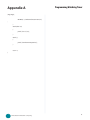
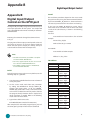
RMA Service Request Form
When requesting RMA service, please fill out the following form.
this form enclosed, your RMA cannot be processed.
Company:
Reasons to Return: Ŀ Repair(Please include failure details)
Ŀ Testing Purpose
Contact Person:
Phone No.
Purchased Date:
Fax No.:
Applied Date:
RMA No:
Return Shipping Address:
Shipping by: Ŀ Air Freight
Ŀ Sea
Ŀ Others:________________
Item
Model Name
Item
Problem Code Failure Status
*Problem Code:
01:D.O.A.
02: Second Time
R.M.A.
03: CMOS Data Lost
04: FDC Fail
05: HDC Fail
06: Bad Slot
Ŀ Express
Serial Number
07:
08:
09:
10:
11:
12:
BIOS Problem
Keyboard Controller Fail
Cache RMA Problem
Memory Socket Bad
Hang Up Software
Out Look Damage
Request Party
Authorized Signature / Date
Embedded and Industrial Computing
Without
___
Configuration
13:
14:
15:
16:
17:
18:
SCSI
LPT Port
PS2
LAN
COM Port
Watchdog Timer
19:
20:
21:
22:
23:
24:
DIO
Buzzer
Shut Down
Panel Fail
CRT Fail
Others (Pls specify)
Confirmed By Supplier
Authorized Signature / Date
37