1
SIS Documentation
SIS3302
100 MHz 16-bit Digitizer
SIS3302
100 MHz 16-bit
VME Digitizer
User Manual
SIS GmbH
Harksheider Str. 102A
22399 Hamburg
Germany
Phone: ++49 (0) 40 60 87 305 0
Fax:
++49 (0) 40 60 87 305 20
email: [email protected]
http://www.struck.de
Version: sis3302-M-010E-001-v109 as of 10.07.09
Page 1 of 61
SIS Documentation
SIS3302
100 MHz 16-bit Digitizer
Revision Table:
Revision
0.01
0.04
0.05
0.06
1.00
1.01
1.02
1.03
Date
18.03.06
08.06.06
13.06.06
16.06.06
23.06.06
03.07.07
18.10.07
04.02.08
1.04
14.02.08
1.05
01.07.08
1.06
1.07
1.08
17.08.08
24.11.08
10.12.08
1.09
10.07.09
Page 2 of 61
Modification
Generation from SIS3320
Th
MKI workup
Definition of airflow
First official release
Bug fixes in interrupt control register
DAC load sequence diagram
Design Version: 010B
New Features:
- Average Mode (2,4,8, …, 128)
- 48-bit Timestamp
- Leading edge trigger
Design Version: 010C
Bug fix: odd VME IRQs
Design Version: 010D
New clock source: Second internal 100 MHz
Firmware comment for 2nd internal 100 MHz
Bug fix in sample length register description
Design Version: 010E
New Features:
- ADC value order programmable (little/big endian)
Bug fix in broadcast setup
SIS Documentation
SIS3302
100 MHz 16-bit Digitizer
- Table of contents
1
Table of contents..............................................................................................................3
Introduction .....................................................................................................................5
1.1
2
Related documents............................................................................................................................. 5
Technical Properties/Features...........................................................................................6
2.1
Key functionality............................................................................................................................... 6
2.2
Module design................................................................................................................................... 7
2.2.1
Dual channel group .................................................................................................................... 8
2.3
Modes of Operation ........................................................................................................................... 8
2.4
Memory management ........................................................................................................................ 8
2.4.1
Single Event Mode..................................................................................................................... 8
2.4.2
Multi Event Mode...................................................................................................................... 8
2.5
Clock sources .................................................................................................................................... 9
2.5.1
Internal clock ............................................................................................................................. 9
2.5.2
External clock ............................................................................................................................ 9
2.6
Trigger control (pre/post, start/stop mode).......................................................................................... 9
2.7
Internal Trigger generation............................................................................................................... 10
2.8
VME Interrupts ............................................................................................................................... 10
3
VME Addressing ...........................................................................................................11
3.1
4
Address Map ................................................................................................................................... 12
Register Description.......................................................................................................14
4.1
Control/Status Register(0x, write/read)............................................................................................. 14
4.2
Module Id. and Firmware Revision Register (0x4, read) ................................................................... 15
4.2.1
Major revision numbers............................................................................................................ 15
4.3
Interrupt configuration register (0x8) ............................................................................................... 16
4.3.1
IRQ mode ................................................................................................................................ 16
4.4
Interrupt control register (0xC)......................................................................................................... 17
4.5
Acquisition control register (0x10, read/write).................................................................................. 19
4.6
Start Delay register (0x14, read/write).............................................................................................. 21
4.7
Stop Delay register (0x18, read/write) .............................................................................................. 21
4.8
Max_Nof_Events_Register (0x20, read/write).................................................................................. 22
4.9
Actual_Event_Counter (0x24, read) ................................................................................................ 22
4.10 CBLT/Broadcast setup register ........................................................................................................ 23
4.11 ADC Memory Page register............................................................................................................. 24
4.12 DAC Control Registers.................................................................................................................... 25
4.12.1 DAC Control/Status register (read/write) .................................................................................. 25
4.12.2 DAC Data register (read/write)................................................................................................ 26
4.12.3 DAC load sequence (read/write).............................................................................................. 26
4.13 Key address general reset................................................................................................................. 28
4.14 Key address VME arm sampling logic ............................................................................................. 28
4.15 Key address VME disarm sampling logic......................................................................................... 28
4.16 Key address VME start sampling ..................................................................................................... 28
4.17 Key address VME stop sampling ..................................................................................................... 28
4.18 Key address Timestamp Clear (0x42C) ............................................................................................ 28
4.19 Event Timestamp directory .............................................................................................................. 29
4.20 Event configuration registers............................................................................................................ 30
4.20.1 Averaging mode....................................................................................................................... 31
4.20.2 Wrap Page size ........................................................................................................................ 32
4.21 Event Length register....................................................................................................................... 33
4.22 Sample Start address register ........................................................................................................... 34
4.22.1 Explanation (sample start address)........................................................................................ 34
4.23 ADC Input mode register................................................................................................................. 35
4.24 ADC1-8 Next Sample address register ............................................................................................. 36
4.25 Actual Sample Value registers ......................................................................................................... 37
4.26 DDR2 Memory Logic Verification registers..................................................................................... 37
4.27 Trigger setup register registers ......................................................................................................... 38
4.28 Threshold registers .......................................................................................................................... 39
Page 3 of 61
SIS Documentation
SIS3302
100 MHz 16-bit Digitizer
4.28.1 Leading edge Trigger ............................................................................................................... 39
4.28.2 FIR Trigger.............................................................................................................................. 40
4.29 Trigger Flag Clear Counter register.................................................................................................. 41
4.30 Event directories.............................................................................................................................. 42
4.31 ADC memory .................................................................................................................................. 43
5
Description of Start/Stop modes of operation .................................................................44
5.1
5.2
6
7
Start logic summary......................................................................................................................... 44
Stop logic summary ......................................................................................................................... 45
Board layout ..................................................................................................................46
Front panel.....................................................................................................................47
7.1
7.2
7.3
7.4
8
Control In/Outputs........................................................................................................................... 48
LED's .............................................................................................................................................. 49
Channel LED's ................................................................................................................................ 49
PCB LEDs....................................................................................................................................... 49
Jumpers/Configuration ...................................................................................................50
8.1
8.2
8.3
8.4
8.5
8.6
CON100 JTAG................................................................................................................................ 50
JP80 VME addressing mode/reset behaviour .................................................................................... 50
JP101 JTAG chain........................................................................................................................... 51
JP102 JTAG source ......................................................................................................................... 52
JP120A-JP120D control input termination ....................................................................................... 53
SW1 and SW2, VME base address................................................................................................... 53
9 Getting started................................................................................................................54
10 Appendix ....................................................................................................................55
10.1 Power consumption ......................................................................................................................... 55
10.2 Operating conditions........................................................................................................................ 55
10.2.1 Cooling.................................................................................................................................... 55
10.2.2 Hot swap/live insertion............................................................................................................. 55
10.3 Connector types............................................................................................................................... 56
10.4 P2 row A/C pin assignments ............................................................................................................ 56
10.5 Row d and z Pin Assignments.......................................................................................................... 57
10.6 Firmware upgrade............................................................................................................................ 58
10.6.1 Upgrade over CON100............................................................................................................. 58
10.6.2 Upgrade over VME.................................................................................................................. 58
11
Index ..........................................................................................................................59
Page 4 of 61
SIS Documentation
1
SIS3302
100 MHz 16-bit Digitizer
Introduction
The SIS3302 is an eight channel ADC/digitizer board with a sampling rate of up to 100 MHz
(for the individual channel) and a resolution of 16-bit. The board is a single width 6U VME
card, which has no special (i.e. non standard VME) voltage requirements.
The flexible combination of DDR2 memory technology data storage in combination with
FPGA based data handling/movement allows for a generic design which covers a variety of
applications.
Applications comprise but are not limited to:
digitization of “slow” detectors like calorimeters
accelerator/machine controls
As we are aware, that no manual is perfect, we appreciate your feedback and will try to
incorporate proposed changes and corrections as quickly as possible. The most recent version
of this manual can be obtained by email from [email protected], the revision dates are online
under http://www.struck.de/manuals.htm.
1.1 Related documents
A list of available firmware designs can be retrieved from
http://www.struck.de/sis3302firm.htm
Page 5 of 61
SIS Documentation
SIS3302
100 MHz 16-bit Digitizer
2 Technical Properties/Features
2.1 Key functionality
Find below a list of key features of the SIS3302 digitizer.
8 channels
16-bit resolution
32 MSamples/channel memory
external clock range 1 ... 100 MHz
special clock mode (random external clock)
external/internal clock
input bandwidth 50 MHz
offset DACs
multi event mode
read on the fly (actual sample value)
pre/post trigger option
readout in parallel to acquisition
trigger generation (FIR trigger)
4 NIM control inputs/4 NIM control outputs
A32 D32/BLT32/MBLT64/2eVME/2eSST
Hot swap (in conjunction with VME64x backplane)
VME64x Connectors
VME64x Front panel
VME64x extractor handles (on request)
F1002 compatible P2 row A/C assignment
+5 V, +12V and –12 V VME standard voltages
LEMO00, SMA or LEMO 0S (differential) analog input connectors
default input span of 5V (can be shifted with DAC to accomplish input range settings like
+2.5 V, ... –2.5 V e.g.)
Note: The SIS3302 shall not be operated on P2 row A/C extensions, like VSB e.g. due to the
compatibility to the F1002 FADC modules clock and start/stop distribution scheme.
Page 6 of 61
SIS Documentation
SIS3302
100 MHz 16-bit Digitizer
2.2 Module design
The SIS3302 consists of four identical groups of 2 ADC channels each and a control section
as shown in the simplified block diagram below.
Page 7 of 61
SIS Documentation
SIS3302
100 MHz 16-bit Digitizer
2.2.1 Dual channel group
Two ADC channels form a group, which memory is handled by one Field Programmable
Gate Array (FPGA).
2.3 Modes of Operation
The SIS3302 was developed with maximum flexibility in mind. The FPGA based design of
the card allows to meet the requirements of many readout applications with dedicated
firmware designs in the future. The initial firmware is supposed to furnish you with an easy to
use yet powerful high speed high resolution Flash Analog to Digital Converter (FADC)
implementation, that covers many everyday analog to digital applications.
2.4 Memory management
The memory can be used either as one contiguous memory or as a subdivided multi event
memory. In addition memory depth can be limited in single event operation to match the
requirements of the given application.
2.4.1 Single Event Mode
The full memory of 32 MSamples of the SIS3302 is used as one big circular buffer or as
single shot memory in single event mode, unless memory size is limited by the event
configuration register.
2.4.2 Multi Event Mode
The memory can be divided in pages or events to make the acquisition of shorter signals
more efficient. Up to 512 stop pointers for the individual page can be retrieved from the event
directory. In auto start mode the ADC advances to the next page and starts sampling
automatically.
Page 8 of 61
SIS Documentation
SIS3302
100 MHz 16-bit Digitizer
2.5 Clock sources
The SIS3302 features the two basic clock modes
Internal clock
External symmetric clock
Random external clock
2.5.1 Internal clock
The internal clock is generated from an on board 50 MHz quartz. It is either doubled or
prescaled to generate 100 MHz or lower clock speeds respectively. A 100 MHz quartz is
available as 2nd internal 100 MHz clock source from firmware revision 0x010D on with the
corresponding stuffing option (i.e. U212 stuffed with a 100 MHz 3.3 V oscillator, Struck part
number 02954)
Internal clock speeds
100 MHz
Second 100 MHz (0x010D)
50 MHz
25 MHz
10 MHz
1 MHz
For optimum internal clock speed resolution the use of the “Second internal 100 MHz”
instead of “internal 100 MHz is recommended.
Prerequisites for the availability of the 2nd 100 MHz:
1.) U212 stuffed with a 100 MHz 3.3 V oscillator
2.) Firmware revision 0x010D or higher
2.5.2 External clock
A symmetric external clock (NIM level, ratio between 45:55 and 55:45) can be fed to the
module through a LEMO00 connector. An ECL clock over rows A/C of the J2 VME
backplane is prepared but not implemented. For optimum performance the clock frequency
should be within the specified range for the given ADC chip.
Module
SIS3302-100
Min. sym. clock
1 MHz
Max sym. clock
100 MHz
Lower sampling speeds are possible in random external clock mode.
2.6 Trigger control (pre/post, start/stop mode)
The SIS3302 features pre/post trigger capability as well as start/stop mode .
The trigger behaviour is defined by the acquisition control register.
Page 9 of 61
SIS Documentation
2.7
SIS3302
100 MHz 16-bit Digitizer
Internal Trigger generation
The trigger output of the SIS3302 can be either used to interact with external trigger logic or
to base start/stop on a threshold (i.e. one individual threshold per ADC channel) of the
digitized data. Trigger generation can be activated with two conditions:
module armed (i.e. sample clock active, trigger can be used to start acquisition)
module armed and started (trigger can be used to stop acquisition)
The user can select between triggering on the conditions above and below threshold
The trigger is formed with a trapezoidal FIR fiter..
2.8 VME Interrupts
Two registers, the Interrupt configuration and the Interrupt control register, are implemented
for interrupt setup and control.
Two interrupt sources are implemented:
- End of Event
- End of Last Event in Multi Event mode
Page 10 of 61
SIS Documentation
3
SIS3302
100 MHz 16-bit Digitizer
VME Addressing
As the SIS3302 VME FADC features memory options with up to 8 times 32 MSamples, A32
addressing was implemented as the only option. The module occupies an address space of
0x7FFFFFF Bytes, i.e. 128 MBytes are used by the module.
The base address is defined by the selected addressing mode, which is selected by jumper
array JP80 and SW1 and SW2 (in non geographical mode).
The table below summarises the possible base address settings.
J1 Setting
Bits
A32 GEO VIPA 31 30 29 28 27
x
SW1
SW2=0...7
Bit 27=0
x
SW1
SW2=8...F
Bit 27=1
x
x
Not implemented in this design
x
Shorthand
SW1/SW2
Not implemented in this design
Explanation
Setting of rotary switch SW1 or SW2 respective
Notes:
This concept allows the use of the SIS3302 in standard VME as well as in VME64x
environments, i.e. the user does not need to use a VME64x backplane.
The factory default setting is EN_A32 closed, SW1=3, SW2=0 (i.e. the module will react
to A32 addressing under address 0x30000000). With more than one unit shipped in one
batch a set of addresses (like 0x10000000, 0x20000000, 0x30000000,...) may be used
also.
Page 11 of 61
SIS Documentation
SIS3302
100 MHz 16-bit Digitizer
3.1 Address Map
The SIS3302 resources and their locations are listed in the table below.
Note: Write access to a key address (KA)with arbitrary data invokes the respective action
Offset
Size in
Bytes
BLT
Access
Function
0x00000000
0x00000004
0x00000008
0x0000000C
4
4
4
4
-
W/R
R
R/W
R/W
Control/Status Register (J-K register)
Module Id. and Firmware Revision register
Interrupt configuration register
Interrupt control register
0x00000010
0x00000014
0x00000018
4
4
4
-
R/W
R/W
R/W
Acquisition control/status register (J-K register)
Extern Start Delay register
Extern Stop Delay register
R/W
R
Max. Nof Events Register
Actual Event Counter
0x00000020
0x00000024
0x00000030
0x00000034
4
4
-
R/W
R/W
CBLT/Broadcast Setup register
ADC Memory Page register
0x00000050
0x00000054
4
4
-
R/W
R/W
DAC Control Status register
DAC Data register
R/W
W
XILINX JTAG_TEST/JTAG_DATA_IN
XILINX JTAG_CONTROL
0x00000060
0x00000064
0x00000400
4
-
KA W
Key General Reset
0x00000410
0x00000414
0x00000418
0x0000041C
4
4
4
4
-
KA W
KA W
KA W
KA W
Key Arm Sampling Logic
Key Disarm Sampling Logic
Key sampling
Key Stop sampling
0x0000042C
4
-
KA W
Key Timestamp Clear
0x00010000
0x1000
D32,
BLT32
R
Event information all ADC groups
0x01000000
4
0x01000004
4
0x01000008
4
0x0100000C
4
-
Page 12 of 61
W only
W only
W only
W only
Event Timestamp directory
Event configuration register (all ADCs)
Event Length register (all ADCs)
Sample Start address register (all ADCs)
ADC input mode register (all ADCs)
SIS Documentation
SIS3302
100 MHz 16-bit Digitizer
Event information ADC group 1
0x02000000
4
0x02000004
4
0x02000008
4
0x0200000C
4
-
R/W
R/W
R/W
R/W
Event configuration register (ADC1, ADC2)
Event Length register (ADC1, ADC2)
Sample Start address register (ADC1, ADC2)
ADC input mode register (ADC1, ADC2)
0x02000010
0x02000014
4
4
-
R
R
Next Sample address register ADC1
Next Sample address register ADC2
0x02000020
0x02000024
0x02000028
4
4
4
-
R
R
R
Actual Sample Value (ADC1, ADC2)
internal Test register
DDR2 Memory Logic Veryfication register
(ADC1, ADC2)
0x0200002C
4
R/W
Trigger Flag Clear Counter register (ADC1,
ADC2)
0x02000030
0x02000034
0x02000038
0x0200003C
4
4
4
4
R/W
R/W
R/W
R/W
ADC1 Trigger setup register
ADC1 Trigger Threshold register
ADC2 Trigger setup register
ADC2 Trigger Threshold register
0x02010000
0x02018000
0x800 D32,
BLT32
0x800 D32,
BLT32
R
Event directory ADC1
R
Event directory ADC2
Event information ADC group 2
0x02800000
4
And so on (as for ADC group 1)
-
R/W
Event configuration register (ADC3, ADC4)
Event information ADC group 3
0x03000000
4
And so on (as for ADC group 1)
-
R/W
Event configuration register (ADC5, ADC6)
Event information ADC group 4
0x03800000
4
And so on (as for ADC group 1)
-
R/W
Event configuration register (ADC7, ADC8)
X
X
X
X
X
X
X
X
R
R
R
R
R
R
R
R
ADC memory pages
0x04000000
0x04800000
0x05000000
0x05800000
0x06000000
0x06800000
0x07000000
0x07800000
8 MByte
8 MByte
8 MByte
8 MByte
8 MByte
8 MByte
8 MByte
8 MByte
ADC 1 memory page
ADC 2 memory page
ADC 3 memory page
ADC 4 memory page
ADC 5 memory page
ADC 6 memory page
ADC 7 memory page
ADC 8 memory page
Note 2: MBLT64, 2eVME and 2eSST read access is supported from memory (i.e. not from
register space) only.
Page 13 of 61
SIS Documentation
SIS3302
100 MHz 16-bit Digitizer
4 Register Description
The function of the individual registers is described in detail in this section.
The first line after the subsection header (in Courier font) like:
#define SIS3302_CONTROL_STATUS
0x0
/* read/write; D32 */
refers to the sis3302.h header file.
4.1
Control/Status Register(0x, write/read)
#define SIS3302_CONTROL_STATUS
0x0
/* read/write; D32 */
The control register is implemented as a selective J/K register, a specific function is enabled
by writing a 1 into the set/enable bit, the function is disabled by writing a 1 into the
clear/disable bit (which location is 16-bit higher in the register). An undefined toggle status
will result from setting both the enable and disable bits for a specific function at the same
time. The only function at this point in time is user LED on/off.
On read access the same register represents the status register.
Bit
31
30
29
28
27
26
25
24
23
22
21
20
19
18
17
16
15
14
13
12
11
10
9
8
7
6
5
4
3
2
1
0
write Function
Clear reserved 15 (*)
Clear reserved 14 (*)
Clear reserved 13 (*)
Clear reserved 12 (*)
Clear reserved 11 (*)
Clear reserved 10 (*)
Clear reserved 9 (*)
Clear reserved 8 (*)
Clear reserved 7 (*)
Clear reserved 6 (*)
Clear reserved 5 (*)
Clear reserved 4 (*)
Clear reserved 3 (*)
Clear reserved 2 (*)
Clear reserved 1 (*)
Switch off user LED (*)
Set reserved 15
Set reserved 14
Set reserved 13
Set reserved 12
Set reserved 11
Set reserved 10
Set reserved 9
Set reserved 8
Set reserved 7
Set reserved 7
Set reserved 7
Set reserved 7
Set reserved 3
Set reserved 2
Set reserved 1
Switch on user LED
(*) denotes power up default setting
Page 14 of 61
read Function
0
0
0
0
0
0
0
0
0
0
0
0
0
0
0
0
Status reserved 15
Status reserved 14
Status reserved 13
Status reserved 12
Status reserved 11
Status reserved 10
Status reserved 9
Status reserved 8
Status reserved 7
Status reserved 6
Status reserved 4
Status reserved 4
Status reserved 3
Status reserved 2
Status reserved 1
Status User LED (1=LED on, 0=LED off)
SIS Documentation
4.2
SIS3302
100 MHz 16-bit Digitizer
Module Id. and Firmware Revision Register (0x4, read)
#define SIS3302_MODID
0x4
/* read only; D32 */
This register reflects the module identification of the SIS3302 and its minor and major
firmware revision levels. The major revision level will be used to distinguish between
substantial design differences and experiment specific designs, while the minor revision level
will be used to mark user specific adaptations.
Bit
31
30
29
28
27
26
25
24
23
22
21
20
19
18
17
16
15
14
13
12
11
10
9
8
7
6
5
4
3
2
1
0
Function
Module Id. Bit 15
Module Id. Bit 14
Module Id. Bit 13
Module Id. Bit 12
Module Id. Bit 11
Module Id. Bit 10
Module Id. Bit 9
Module Id. Bit 8
Module Id. Bit 7
Module Id. Bit 6
Module Id. Bit 5
Module Id. Bit 4
Module Id. Bit 3
Module Id. Bit 2
Module Id. Bit 1
Module Id. Bit 0
Major Revision Bit 7
Major Revision Bit 6
Major Revision Bit 5
Major Revision Bit 4
Major Revision Bit 3
Major Revision Bit 2
Major Revision Bit 1
Major Revision Bit 0
Minor Revision Bit 7
Minor Revision Bit 6
Minor Revision Bit 5
Minor Revision Bit 4
Minor Revision Bit 3
Minor Revision Bit 2
Minor Revision Bit 1
Minor Revision Bit 0
Reading
3
3
0
2
4.2.1 Major revision numbers
Find below a table with major revision numbers used to date
Major revision number
0x01
0x20
Application/user
Generic designs
Gamma design
Page 15 of 61
SIS Documentation
SIS3302
100 MHz 16-bit Digitizer
4.3 Interrupt configuration register (0x8)
#define SIS3302_IRQ_CONFIG
0x8
/* read/write; D32 */
This read/write register controls the VME interrupt behaviour of the SIS3302 ADC. Four
interrupt sources are foreseen, for the time being three of them are associated with an interrupt
condition, the fourth condition is reserved for future use.
The interrupter type is DO8 .
4.3.1 IRQ mode
In RORA (release on register access) mode the interrupt will be pending until the IRQ
source is cleared by specific access to the corresponding disable VME IRQ source bit. After
the interrupt is serviced the source has to be activated with the enable VME IRQ source bit
again.
In ROAK (release on acknowledge) mode , the interrupt condition will be cleared (and the
IRQ source disabled) as soon as the interrupt is acknowledged by the CPU. After the interrupt
is serviced the source has to be activated with the enable VME IRQ source bit again.
Bit
31
...
16
15
14
13
12
11
10
9
8
7
6
5
4
3
2
1
0
Function
RORA/ROAK Mode (0: RORA; 1: ROAK)
VME IRQ Enable (0=IRQ disabled, 1=IRQ enabled)
VME IRQ Level Bit 2
VME IRQ Level Bit 1
VME IRQ Level Bit 0
IRQ Vector Bit 7; placed on D7 during VME IRQ ACK cycle
IRQ Vector Bit 6; placed on D6 during VME IRQ ACK cycle
IRQ Vector Bit 5; placed on D5 during VME IRQ ACK cycle
IRQ Vector Bit 4; placed on D4 during VME IRQ ACK cycle
IRQ Vector Bit 3; placed on D3 during VME IRQ ACK cycle
IRQ Vector Bit 2; placed on D2 during VME IRQ ACK cycle
IRQ Vector Bit 1; placed on D1 during VME IRQ ACK cycle
IRQ Vector Bit 0; placed on D0 during VME IRQ ACK cycle
The power up default value reads 0x 00000000
Page 16 of 61
Default
0
0
0
0
0
0
0
0
0
0
0
0
0
0
0
0
0
0
0
SIS Documentation
SIS3302
100 MHz 16-bit Digitizer
4.4 Interrupt control register (0xC)
#define SIS3302_IRQ_CONTROL
0xC
/* read/write; D32 */
This register controls the VME interrupt behaviour of the SIS3302 ADC. Eight interrupt
sources are foreseen, for the time being two of them are associated with an interrupt
condition, the others are reserved for future use.
Bit
31
30
29
28
27
26
25
Function (w)
Update IRQ Pulse
unused
unused
unused
unused
unused
unused
24
23
22
21
20
19
18
17
16
15
14
13
12
11
10
9
8
7
6
5
4
3
2
1
0
unused
Disable/Clear IRQ source 7
Disable/Clear IRQ source 6
Disable/Clear IRQ source 5
Disable/Clear IRQ source 4
Disable/Clear IRQ source 3
Disable/Clear IRQ source 2
Disable/Clear IRQ source 1
Disable/Clear IRQ source 0
unused
unused
unused
unused
unused
unused
unused
unused
Enable IRQ source 7
Enable IRQ source 6
Enable IRQ source 5
Enable IRQ source 4
Enable IRQ source 3
Enable IRQ source 2
Enable IRQ source 1
Enable IRQ source 0
(r)
Status IRQ source 7 (reserved)
Status IRQ source 6 (reserved)
Status IRQ source 5 (reserved)
Status IRQ source 4 (reserved)
Status IRQ source 3 (reserved)
Status IRQ source 2 (reserved)
Status IRQ source 1 (End of Last Event in Multi Event mode;
edge sensitive)
Status IRQ source 0 (End of Event; edge sensitive)
Status flag source 7
Status flag source 6
Status flag source 5
Status flag source 4
Status flag source 3
Status flag source 2
Status flag source 1
Status flag source 0
Status VME IRQ
Status internal IRQ
0
0
0
0
0
0
Status enable source 7 (read as 1 if enabled, 0 if disabled)
Status enable source 6 (read as 1 if enabled, 0 if disabled)
Status enable source 5 (read as 1 if enabled, 0 if disabled)
Status enable source 4 (read as 1 if enabled, 0 if disabled)
Status enable source 3 (read as 1 if enabled, 0 if disabled)
Status enable source 2 (read as 1 if enabled, 0 if disabled)
Status enable source 1 (read as 1 if enabled, 0 if disabled)
Status enable source 0 (read as 1 if enabled, 0 if disabled)
Default
0
0
0
0
0
0
0
0
0
0
0
0
0
0
0
0
0
0
0
0
0
0
0
0
0
0
0
0
0
0
0
0
The power up default value reads 0x00000000
Page 17 of 61
SIS Documentation
SIS3302
100 MHz 16-bit Digitizer
The generation of the status flags, the IRQ flags and the actual IRQ is illustrated with the
schematic below:
IRQ source 0:
IRQ source 1:
IRQ source 2:
IRQ source 3:
End of Event
End of Last Event in Multi Event mode (disarm)
reserved
reserved
IRQ source 4:
IRQ source 5:
IRQ source 6:
IRQ source 7:
reserved
reserved
reserved
reserved
Page 18 of 61
SIS Documentation
4.5
SIS3302
100 MHz 16-bit Digitizer
Acquisition control register (0x10, read/write)
#define SIS3302_ACQUISTION_CONTROL
0x10
/* read/write; D32 */
The acquisition control register is in charge of most of the settings related to the actual
configuration of the digitization process.
Like the control register it is implemented in a J/K fashion.
Bit
31
30
29
28
27
26
25
24
23
22
21
20
19
18
17
16
15
14
13
12
11
10
9
Write Function
Clear reserved 15 (*)
Clear Clock Source Bit2
Clear Clock Source Bit1
Clear Clock Source Bit0
Clear ADC value order big endian (*)
Clear reserved 10 (*)
Disable front panel Lemo Timestamp_Clear (Lemo In 1) (*)
Disable front panel LEMO start/stop logic
Clear reserved 7 (*)
Disable internal trigger as stop (*)
Disable Multi Event mode (*)
Disable Autostart mode (*)
Clear reserved 3 (*)
Clear reserved 2 (*)
Clear reserved 1 (*)
Clear reserved 0 (*)
Set reserved 15
Set clock source Bit 2
Set clock source Bit 1
Set clock source Bit 0
Set ADC value order big endian
Set reserved 10
Enable front panel Lemo Timestamp_Clear (Lemo In 1)
8
7
6
5
Enable front panel Lemo Start/Stop logic
Set reserved 7
Enable internal trigger as stop
Enable Multi Event mode
Read
0
0
0
0
0
0
0
0
0
0
0
0
0
0
ADC Sampling Busy
ADC Sampling Logic Armed
Status reserved 15
Status clock source Bit 2
Status clock source Bit 1
Status clock source Bit 0
Status ADC value order big endian
Status reserved 10
Status Enable front panel Lemo
Timestamp_Clear
Status Enable front panel start/stop logic
Status reserved 7
Status internal trigger as stop
Status Multi Event mode
4
Enable Autostart mode
Status Autostart mode
3
2
1
0
Set reserved 3
Set reserved 2
Set reserved 1
Set reserved 0
Status reserved 3
Status reserved 2
Status reserved 1
Status reserved 0
The power up default value reads 0x0
Page 19 of 61
SIS Documentation
SIS3302
100 MHz 16-bit Digitizer
Clock source bit setting table:
Clock Source
Bit2
0
0
0
0
1
1
1
1
Clock Source
Bit1
0
0
1
1
0
0
1
1
Clock Source
Bit0
0
1
0
1
0
1
0
1
Clock Source
internal 100 MHz
internal 50 MHz
internal 25 MHz
internal 10 MHz
internal 1 MHz
external random clock mode (internal 100 MHz)
external clock (LEMO front panel) ; min. 1 MHz
Second internal 100 MHz
Note:
The internal 100 MHz is generated with a DLL in the FPGA from the internal 50 MHz.
For optimum resolution use the “Second internal 100 MHz” instead of “internal 100 MHz”.
(U212 must be assembled with a 100 MHz 3.3 V oscillator)
Multi Event mode :
0 : Sampling Logic Armed state will be cleared at end of
event
1 : Sampling Logic Armed state will be cleared at end of
last event (defined with Max_Nof_Events register)
Autostart mode:
0 : The Sampling will start when the Sampling Logic is armed and a
START is issued (external LEMO or VME KEY command).
1 : With Multi Event Mode enabled sampling will start with the Sampling Logic Arm
command (VME KEY command) and with end of Event. to start sampling.
Sampling will start in the next page in the latter case.
External random clock mode :
This mode allows for sampling at arbitrary low and non symmetric external clock. The
digitizer is set up for internal clock and will strobe one datum to memory with the leading
edge of the internal clock cycle that follows the leading edge of an external clock pulse as
illustrated below. Pipelining between the actual analog input signal and the value stored to
memory has to be taken into account.
External Clock
Internal Clock
Clock to Memory
ADC value order big endian mode:
0 : The ADC value readout order is little endian
1 : The ADC value readout order is big endian
Page 20 of 61
SIS Documentation
SIS3302
100 MHz 16-bit Digitizer
(see ADC Memory Data Format)
.
4.6
Start Delay register (0x14, read/write)
#define SIS3302_START_DELAY
0x14
/* read/write; D32 */
Pretrigger operation can be implemented via the start delay register in conjunction with front
panel start/stop mode operation. The external Start Signal and the Autostart Signal will be
delayed by the value of the register .
Bit
31
...
24
23
..
..
0
unused, read as 0
unused, read as 0
START_DELAY_BIT23
START_DELAY_BIT0
The power up default value is 0
4.7
Stop Delay register (0x18, read/write)
#define SIS3302_STOP_DELAY
0x18
/* read/write; D32 */
Posttrigger operation can be implemented via the stop delay register in conjunction with front
panel start/stop mode operation. The external stop signal and the internal trigger (if enabled)
will be delayed by the value of the register .
Bit
31
...
24
23
..
..
0
unused, read as 0
unused, read as 0
STOP_DELAY_BIT23
STOP _DELAY_BIT0
The power up default value is 0
Page 21 of 61
SIS Documentation
4.8
SIS3302
100 MHz 16-bit Digitizer
Max_Nof_Events_Register (0x20, read/write)
#define SIS3302_MAX_NOF_EVENT
0x20
/* read/write; D32 */
The Sampling Logic will be disarmed In Multi Event mode as soon as the Event counter
reaches the value of the Max_Nof_Events register.
Bit
31
...
20
19
..
..
0
unused, read as 0
unused, read as 0
MAX NOF Events Bit19
MAX NOF Events Bit 0
The power up default value is 0
4.9 Actual_Event_Counter (0x24, read)
#define SIS3302_ACTUAL_EVENT_COUNTER
0x24
/* read; D32 */
This register holds the actual number of events in multi event mode.
The Event Counter is cleared when the Sampling Logic is armed and it is incremented with
every start sampling.
Bit
31
...
20
19
..
..
0
unused, read as 0
unused, read as 0
Actual event counter Bit 19
Actual event counter Bit 0
The power up default value is 0
Page 22 of 61
SIS Documentation
SIS3302
100 MHz 16-bit Digitizer
4.10 CBLT/Broadcast setup register
#define SIS3302_CBLT_BROADCAST_SETUP
0x30
/* read/write; D32 */
The CBLT feature is not implemented yet (as of firmware 01 06).
This read/write register defines, whether the SIS3302 will participate in a Broadcast. The
configuration of this register and the registers of other participating modules is essential for
proper Broadcast behaviour.
Bit
31
30
29
28
27
26
25
24
23
22
21
20
19
18
17
16
15
14
13
12
11
10
9
8
7
6
5
4
3
2
1
0
Function
CBLT/Broadcast address bit 31
CBLT/Broadcast address bit 30
CBLT/Broadcast address bit 29
CBLT/Broadcast address bit 28
CBLT/Broadcast address bit 27
reserved
reserved
reserved
reserved
reserved
reserved
reserved
reserved
reserved
reserved
reserved
reserved
reserved
reserved
reserved
reserved
0
0
0
0
0
Enable Broadcast Master
Enable Broadcast
0
reserved
reserved
reserved
Page 23 of 61
SIS Documentation
SIS3302
100 MHz 16-bit Digitizer
4.11 ADC Memory Page register
#define SIS3302_ADC_MEMORY_PAGE_REGISTER 0x34
/* read/write; D32 */
The SIS3302 default memory size per channel is 64 MByte (i.e. 32 MSample).
The VME address space window per ADC is limited to 8 MByte (4 MSample) however. The
read/write ADC memory page register is used to select one of the 8 memory subdivisions
(pages).
Bit
31
..
..
4
3
2
1
0
Function
reserved
reserved
Page register bit 3 (reserved)
Page register bit 2
Page register bit 1
Page register bit 0
Example: readout routine for 32MSample readout
(see sis3302_single_event_sample_wrap_test1.c)
int sis3302_Read_ADC_Channel(
Page 24 of 61
unsigned
unsigned
unsigned
unsigned
unsigned
unsigned
int module_address,
int vme_read_mode,
int adc_channel /* 0 to 7 */,
int event_sample_start_addr,
int event_sample_length,
int* uint_adc_buffer)
SIS Documentation
SIS3302
100 MHz 16-bit Digitizer
4.12 DAC Control Registers
This set of registers is used to program the 16-bit offset DACs for the 8 ADC channels. Refer
to the documentation of the AD5570 DAC chip for details also and have a look to the
configuration example in sis3302_adc_test1.c (CVI directory)
Example routine:
int sis3302_write_dac_offset( unsigned int module_addr,
unsigned int *offset_value_array)
4.12.1 DAC Control/Status register (read/write)
#define SIS3302_DAC_CONTROL_STATUS 0x50
Bit
31
..
..
16
15
14
...
8
7
6
5
4
3
2
1
0
Write Function
None
..
..
None
None
None
None
None
DAC selection Bit 2
DAC selection Bit 1
DAC selection Bit 0
..
none
DAC Command Bit 1
DAC Command Bit 0
/* read/write; D32 */
Read Function
0
..
..
0
DAC Read/Write/Clear Cycle BUSY
0
...
0
0
status of DAC selection Bit 2
status of DAC selection Bit 1
status of DAC selection Bit 0
..
0
DAC Command Bit 1 Status
DAC Command Bit 0 Status
DAC Command Bit
Bit 1
0
0
1
1
Bit 0
0
1
0
1
Function
No function
Load shift register of selected DAC
Load selected DAC
Clear all DACs
A “Clear DAC” command (issued after power up automatically) sets the value of all
DACs to analog ground.
Page 25 of 61
SIS Documentation
SIS3302
100 MHz 16-bit Digitizer
4.12.2 DAC Data register (read/write)
#define SIS3302_DAC_DATA
Bit
31
..
..
16
15
..
..
0
Write Function
none
..
..
none
DAC Output Register Bit 15
..
..
DAC Output Register Bit 0
0x54
/* read/write; D32 */
Read Function
DAC Input Register Bit 15 (from DAC)
..
..
DAC Input Register Bit 0
DAC Output Register Bit 15
0
0
DAC Output Register Bit 0
4.12.3 DAC load sequence (read/write)
The sequence to load the DAC of a single channel is shown below.
The example routine sis3302_write_dac_offset loads the 8 DACs of a SIS3302 module
at base address module offset in a loop.
Sequence to load offset of channel N, N=[0,…,7]
dacdata=dacdatum[N]
daccontrol=1 (shift) + N << 4
read dacstatus
until busy==0
daccontrol=2 (load) + N << 4
read dacstatus
until busy==0
Page 26 of 61
SIS Documentation
SIS3302
100 MHz 16-bit Digitizer
Find below a DAC scan that was acquired with the DAC test function of the SIS3302 ADC
Labwindows application. The SIS3302 under test was configured for an input span of some 2
Vpkpk. It can be seen, that a DAC offset of some 37000 counts is required to accomplish an
input range of -1...+1V on this particular channel.
Note: The actual sample value registers can be used to monitor the influence of the DAC
settings on the ADC values.
Page 27 of 61
SIS Documentation
SIS3302
100 MHz 16-bit Digitizer
4.13 Key address general reset
#define SIS3302_KEY_RESET
0x400
/* write only; D32 */
A write with arbitrary data to this register (key address) resets the SIS3302 to it’s power up
state.
4.14 Key address VME arm sampling logic
#define SIS3302_KEY_ARM
0x410
/* write only; D32 */
A write with arbitrary data to this register (key address) will arm the sampling logic.
If Autostart mode is enabled then the sampling will also start.
4.15 Key address VME disarm sampling logic
#define SIS3302_KEY_DISARM
0x414
/* write only; D32 */
A write with arbitrary data to this register (key address) will disarm the sampling logic.
4.16 Key address VME start sampling
#define SIS3302_KEY_START
0x418
/* write only; D32 */
A write with arbitrary data to this register (key address) will initiate if the sampling logic is
armed for sampling.
4.17 Key address VME stop sampling
#define SIS3302_KEY_STOP
0x41C
/* write only; D32 */
A write with arbitrary data to this register (key address) will halt sampling on the active page.
The Sample Logic will be disarmed also in Single Event Mode or if the
Actual_Event_Counter reaches the value of the Max_Nof_Events register.
4.18 Key address Timestamp Clear (0x42C)
#define SIS3302_KEY_TIMESTAMP_CLR
0x42C
/* write only; D32 */
A write with arbitrary data to this register (key address) clears the 48-bit Timestamp counter.
Page 28 of 61
SIS Documentation
SIS3302
100 MHz 16-bit Digitizer
4.19 Event Timestamp directory
#define SIS3302_TIMESTAMP_DIRECTORY
0x10000
/* read only; D32, BLT32; size: 0x1000 */
The event timestamp directory can be used to measure time between triggers (stops) in multi
event mode.
The counter value of the 48-bit wide scaler is written to the corresponding location for
subsequent events. It is stored with the last sampled value. To obtain the time of the
trigger/stop the information from the sample address bits 0 and 1 of the next sample address
register has to be taken into account.
offset address
0x0
0x4
0x8
..
..
..
0xff4
0xff8
0xffc
Timestamp
Upper Timestamp bits (47:32) of Event 1
Lower Timestamp bits (31:0) of Event 1
Upper Timestamp bits (47:32) of Event 2
Lower Timestamp bits (31:0) of Event 511
Upper Timestamp bits (47:32) of Event 512
Lower Timestamp bits (31:0) of Event 512
Page 29 of 61
SIS Documentation
SIS3302
100 MHz 16-bit Digitizer
4.20 Event configuration registers
#define SIS3302_EVENT_CONFIG_ALL_ADC
0x01000000
/* write only;D32 */
#define
#define
#define
#define
0x02000000
0x02800000
0x03000000
0x03800000
/*
/*
/*
/*
SIS3302_EVENT_CONFIG_ADC12
SIS3302_EVENT_CONFIG_ADC34
SIS3302_EVENT_CONFIG_ADC56
SIS3302_EVENT_CONFIG_ADC78
read/write;D32
read/write;D32
read/write;D32
read/write;D32
*/
*/
*/
*/
This register is implemented for each channel group and it has to be written with the same
value, the best way is to make use of the address SIS3302_EVENT_CONFIG_ALL_ADC to write
to the registers of all channel groups simultaneously.
Bit
31
...
28
27
26
25
24
23
16
15
14
13
12
11
...
8
7
6
5
4
3
2
1
0
Function
unused; read 0
...
unused; read 0
unused; read 0
unused; read 0
FPGA Id. 1
FPGA Id. 0
unused; read 0
...
unused; read 0
reserved
Average Mode Bit 2
Average Mode Bit 1
Average Mode Bit 0
reserved
...
reserved
reserved
reserved
Enable Event Length Stop mode
Enable Page Wrap around mode
0 : Wrap around full memory
1 : Wrap around page until STOP (External or KEY or Event Length Stop)
Wrap Page size Bit 3
Wrap Page size Bit 2
Wrap Page size Bit 1
Wrap Page size Bit 0
Enable Event Length Stop mode:
0: no stop from Event Length logic
1: sampling will stop after counts defined in register “Event Length register”.
Enable Page Wrap around mode:
0 : Wrap around full memory (32 MSample)
1 : Wrap around in pages defined by pages size bits
Page 30 of 61
SIS Documentation
SIS3302
100 MHz 16-bit Digitizer
The pages size is defined by this register in wrap event mode. The lowest four bits define the
number of memory divisions as listed in the table below.
FPGA Id. 0/1:
The two bits are used to identify the ADC/FPGA group as shown in the table below.
ADC/FPGA group
ADC78/FPGA3
ADC56/FPGA2
ADC34/FPGA1
ADC12/FPGA0
FPGA Id. 1
1
1
0
0
FPGA Id. 0
1
0
1
0
4.20.1 Averaging mode
Averaging mode is implemented to improve the signal to noise ratio in lower speed
digitization applications. N consecutive samples are summed up in the FPGAs of the dual
channel groups
Averaging mode is activated by specifying a non zero value for bits 14:12 of the event
configuration register(s).
Average Bit 2
0
0
0
0
1
1
1
1
Average Bit 1
0
0
1
1
0
0
1
1
Average Bit 0
0
1
0
1
0
1
0
1
averaged samples
1 (no average)
2
4
8
16
32
64
128
Page 31 of 61
SIS Documentation
SIS3302
100 MHz 16-bit Digitizer
4.20.2 Wrap Page size
The page/event size is defined by the 4 page size bits as follows:
Page size
Bit 3
0
0
0
0
0
0
0
0
1
1
1
1
1
1
1
1
Page 32 of 61
Page size
Bit 2
0
0
0
0
1
1
1
1
0
0
0
0
1
1
1
1
Page size
Bit 1
0
0
1
1
0
0
1
1
0
0
1
1
0
0
1
1
Page size
Bit 0
0
1
0
1
0
1
0
1
0
1
0
1
0
1
0
1
Page size
16 M Samples
4 M Samples
1 M Samples
256 K Samples
64K Samples
16 K Samples
4 K Samples
1 K Samples
512 Samples
256 Samples
128 Samples
64 Samples
reserved
reserved
reserved
reserved
SIS Documentation
SIS3302
100 MHz 16-bit Digitizer
4.21 Event Length register
#define SIS3302_SAMPLE_LENGTH_ALL_ADC
0x01000004
#define
#define
#define
#define
0x02000004
0x02800004
0x03000004
0x03800004
SIS3302_SAMPLE_LENGTH_ADC12
SIS3302_SAMPLE_LENGTH_ADC34
SIS3302_SAMPLE_LENGTH_ADC56
SIS3302_SAMPLE_LENGTH_ADC78
This register defines the number of samples for each event if the “Event Length Stop mode” is
enabled.
Value of Event Length register = (Event Length - 4) & 0xfffffC
Bit
31
...
25
24
..
2
1
0
unused, read as 0
unused, read as 0
Event Length Register BIT24
Event Length Register BIT2
Unused
Unused
The power up default value is 0
Example: Desired event length 0x100 -> set the register to 0xFC
Page 33 of 61
SIS Documentation
SIS3302
100 MHz 16-bit Digitizer
4.22 Sample Start address register
#define SIS3302_SAMPLE_START_ADDRESS_ALL_ADC
0x01000008
#define
#define
#define
#define
0x02000008
0x02800008
0x03000008
0x03800008
SIS3302_SAMPLE_START_ADDRESS_ADC12
SIS3302_SAMPLE_START_ADDRESS_ADC34
SIS3302_SAMPLE_START_ADDRESS_ADC56
SIS3302_SAMPLE_START_ADDRESS_ADC78
These registers define the memory start address.
The value is given in samples (i.e. number of 16-bit words)
Only Sample Start addresses on a 4 16-bit (sample) boundary (i.e. 8 bytes) are valid.
Bit
31
...
25
24
..
2
1
0
unused, read as 0
unused, read as 0
Sample Start Address Register Bit 24
Sample Start Address Register Bit 2
unused
unused
The power up default value is 0
4.22.1 Explanation (sample start address)
The contents of the start sample register is assigned as memory data storage address with the
arm command (key address arm sampling). The user has to distinguish between two the two
wrap modes of the SIS3302.
No Page wrap around mode (event configuration register bit 4 = 0):
Bits 24:2 of the sample start register are used as memory start address upon the arm condition.
The lowest 2 bits are 0 (i.e. the start address is on a 4 sample or 8 byte boundary). The
internal address is incremented by 1 with every sample clock.
The stop will be on a 4 sample boundary.
The next (adjacent) address will be used as the starting point for the next event in multi event
mode.
Page wrap around mode (event configuration register bit 4 = 1):
The upper part of the sample start register (page address) is used as memory start address
upon the arm command. The lower bits (number of bits defined by the page size, bits 9:0 for a
page size of 1K e.g.). The lower portion is incremented by 1 with every sample clock. The
stop will be on a 4 sample boundary also. The exact stop location can be obtained from the
lowest 2 bits of the next sample register or the event directory.
The upper portion of the address (page address) is incremented by 1 with the start of the next
event and the lower portion is cleared again.
Page 34 of 61
SIS Documentation
SIS3302
100 MHz 16-bit Digitizer
4.23 ADC Input mode register
#define SIS3302_ADC_INPUT_MODE_ALL_ADC
0x0100000C
#define
#define
#define
#define
0x0200000C
0x0280000C
0x0300000C
0x0380000C
SIS3302_ADC_INPUT_MODE_ALL_ADC12
SIS3302_ADC_INPUT_MODE_ALL_ADC34
SIS3302_ADC_INPUT_MODE_ALL_ADC56
SIS3302_ADC_INPUT_MODE_ALL_ADC78
This register set is used to generate memory test data.
Bit
31
...
20
19
18
17
16
15
..
0
Function
Unused; read 0
...
Unused; read 0
Test Data 32-bit Mode : 0 = 16-bit mode ; 1 = 32-bit mode
Enable Simulate ADC Test Data Mode
ADC Test Start Data Bit 15
ADC Test Start Data Bit 0
Test Start Data has to be different from 0xYYFE and 0xYYFF.
An increment pattern is recorded in test mode (Bit 16 = 1) instead of real ADC data. Data are
incremented by 2 in 32-bit mode.
Page 35 of 61
SIS Documentation
SIS3302
100 MHz 16-bit Digitizer
4.24 ADC1-8 Next Sample address register
#define
#define
#define
#define
#define
#define
#define
#define
SIS3302_ACTUAL_SAMPLE_ADDRESS_ADC1
SIS3302_ACTUAL_SAMPLE_ADDRESS_ADC2
SIS3302_ACTUAL_SAMPLE_ADDRESS_ADC3
SIS3302_ACTUAL_SAMPLE_ADDRESS_ADC4
SIS3302_ACTUAL_SAMPLE_ADDRESS_ADC5
SIS3302_ACTUAL_SAMPLE_ADDRESS_ADC6
SIS3302_ACTUAL_SAMPLE_ADDRESS_ADC7
SIS3302_ACTUAL_SAMPLE_ADDRESS_ADC8
0x02000010
0x02000014
0x02800010
0x02800014
0x03000010
0x03000014
0x03800010
0x03800014
These 8 read only registers hold the next sampling address for the given channel.
Bit
31
...
25
24
..
2
1
0
Function
unused, read as 0
unused, read as 0
Sample Address Bit 24
Sample Address Bit 2
Sample Address Bit 1*
Sample Address Bit 0*
The power up default value is 0
* Sample address bits 1 and 0 have a dedicated meaning.
Explanation:
Data are stored to memory in packets of 4 consecutive samples by the sample logic. This
implies, that either one additional sample is stored in stop mode (wrap mode respective ) or
that the last 1-2 samples before the stop are not stored.
Sample address bits 1:0 can be used to obtain the position of the stop signal within the 4
sample packet.
The stop delay can be used to make sure, that all samples up to the external stop condition are
written to memory.
Sample Address
Bits 1:0
3
0
1
2
Page 36 of 61
Correction
-1
0
+1
+2
SIS Documentation
SIS3302
100 MHz 16-bit Digitizer
4.25 Actual Sample Value registers
#define
#define
#define
#define
SIS3302_ACTUAL_SAMPLE_VALUE_ADC12
SIS3302_ACTUAL_SAMPLE_VALUE_ADC34
SIS3302_ACTUAL_SAMPLE_VALUE_ADC56
SIS3302_ACTUAL_SAMPLE_VALUE_ADC78
0x02000020
0x02800020
0x03000020
0x03800020
Read “on the fly” of the actual converted ADC values.
The read only registers are updated with every ADC clock, unless a concurrent VME read
access is pending.
The register contents is refreshed and can be read any time (i.e. they are updated independent
of the unarmed, armed, sampling state) as long as a sampling clock is distributed on the ADC
board (internal clock or active/clocking external clock)
ADC 1 / 3 / 5 / 7
D31:16
16-bit data
ADC 2 / 4 / 6 / 8
D15:0
16-bit data
4.26 DDR2 Memory Logic Verification registers
#define
#define
#define
#define
SIS3302_DDR2_TEST_REGISTER_ADC12
SIS3302_DDR2_TEST_REGISTER_ADC34
SIS3302_DDR2_TEST_REGISTER_ADC56
SIS3302_DDR2_TEST_REGISTER_ADC78
0x02000028
0x02800028
0x03000028
0x03800028
D31:28
Fifo_11_wr_addr
ADC 2 / 4 / 6 / 8
D27:24
D23:20
Fifo_10_wr_addr
Fifo_01_wr_addr
D19:16
Fifo_00_wr_addr
D15:12
Fifo_11_wr_addr
ADC 1 / 3 / 5 / 7
D11:8
D7:4
Fifo_10_wr_addr
Fifo_01_wr_addr
D3:0
Fifo_00_wr_addr
This register set can be used to verify proper operation of the DDR2 memory read logic. The
contents of all registers has to be identical. So far no deviation/error condition with firmware
V1.02 has been detected. Please report problems to Struck Innovative Systeme. The error can
be salvaged by issuing a key reset DDR2 memory logic command.
Page 37 of 61
SIS Documentation
SIS3302
100 MHz 16-bit Digitizer
4.27 Trigger setup register registers
#define
#define
#define
#define
#define
#define
#define
#define
SIS3302_TRIGGER_SETUP_ADC1
SIS3302_TRIGGER_SETUP_ADC2
SIS3302_TRIGGER_SETUP_ADC3
SIS3302_TRIGGER_SETUP_ADC4
SIS3302_TRIGGER_SETUP_ADC5
SIS3302_TRIGGER_SETUP_ADC6
SIS3302_TRIGGER_SETUP_ADC7
SIS3302_TRIGGER_SETUP_ADC8
0x02000030
0x02000038
0x02800030
0x02800038
0x03000030
0x03000038
0x03800030
0x03800038
These read/write registers hold the Peaking and Gap Time of the trapezoidal FIR filter.
(Gap Time = SumG Time – Peaking Time)
Bit
Function
31
reserved; read 0
..
..
24
reserved; read 0
23
Puls Length bit 7
22
Puls Length bit 6
21
Puls Length bit 5
20
Puls Length bit 4
19
Puls Length bit 3
18
Puls Length bit 2
17
Puls Length bit 1
16
Puls Length bit 0
15
reserved
14
reserved
13
reserved
12
SumG bit 4
11
SumG bit 3
10
SumG bit 2
9
SumG bit 1
8
SumG bit 0
7
reserved
6
reserved
5
reserved
4
P bit 4
3
P bit 3
2
P bit 2
1
P bit 1
0
P bit 0
The power up default value reads 0x 00000000
Trigger Pulse Length
SumG time
(time between both sums)
Peaking time P
x+P
Si
i=x
Si:
Sum of ADC input sample stream from x to x+P
P:
Peaking time (number of values to sum)
SumG: SumGap time (distance in clock ticks of the two running sums)
The maximum SumG time:
16 (clocks)
The minimun SumG time: 1 (clocks)
Values > 16 will be set to 16
Value = 0 will be set to 1
The maximum Peaking time:
The minimun Peaking time:
Values > 16 will be set to 16
Value = 0 will be set to 1
Page 38 of 61
16 (clocks)
1 (clocks)
Note: ADC raw data are shifted 4
bits to the right for trigger
formation
SIS Documentation
SIS3302
100 MHz 16-bit Digitizer
4.28 Threshold registers
#define
#define
#define
#define
#define
#define
#define
#define
SIS3302_TRIGGER_THRESHOLD_ADC1
SIS3302_TRIGGER_THRESHOLD_ADC2
SIS3302_TRIGGER_THRESHOLD_ADC3
SIS3302_TRIGGER_THRESHOLD_ADC4
SIS3302_TRIGGER_THRESHOLD_ADC5
SIS3302_TRIGGER_THRESHOLD_ADC6
SIS3302_TRIGGER_THRESHOLD_ADC7
SIS3302_TRIGGER_THRESHOLD_ADC8
0x02000034
0x0200003C
0x02800034
0x0280003C
0x03000034
0x0300003C
0x03800034
0x0380003C
These read/write registers hold the threshold values for the ADC channels.
Bit
31-27
Function none
Trigger Mode = 0 :
Trigger Mode = 1 :
26
25
Trigger Mode GT/
GE
24
LT
16-0
Trapezoidal threshold value /
threshold value
FIR Filter trigger
Leading edge trigger
4.28.1 Leading edge Trigger
A Trigger Output pulse is generated on two conditions:
1. if LT is set:
the Trigger Out Pulse will be issued if the actual ADC value goes
below the programmable threshold value.
2. if GE is set:
the Trigger Out Pulse will be issued if the actual ADC value goes
above the programmable threshold value - 1
Page 39 of 61
SIS Documentation
SIS3302
100 MHz 16-bit Digitizer
4.28.2 FIR Trigger
The value of the Sum (trapezoidal value) depends on the peaking time P. Therefore the
selection of the value of the Trapezoidal threshold depends on P also.
See Trigger Example.
Trapezoidal value calculation:
Trapezoidal value = (SUM2 – SUM1) + 0x10000
Where
x+P
Si
SUM1 =
i=x
x+P+sumG
SUM2 =
Sj
j = x+sumG
The FIR Filter logic adds 0x10000 to the result of the subtraction of the two running sums.
This implies, that the internal value of the trapezoid is on average 0x10000.
A Trigger Output pulse is generated on two conditions:
1. LT is set: the Trigger Out Pulse will be issued if the actual trapezoidal value goes below
the programmable trapezoidal threshold value.
2. GT is set: the Trigger Out Pulse will be issued if the actual trapezoidal value goes above
the programmable trapezoidal threshold value
Page 40 of 61
SIS Documentation
SIS3302
100 MHz 16-bit Digitizer
4.29 Trigger Flag Clear Counter register
#define
#define
#define
#define
SIS3302_TRIGGER_FLAG_CLR_CNT_ADC12
SIS3302_TRIGGER_FLAG_CLR_CNT_ADC34
SIS3302_TRIGGER_FLAG_CLR_CNT_ADC56
SIS3302_TRIGGER_FLAG_CLR_CNT_ADC78
0x0200002C
0x0280002C
0x0300002C
0x0380002C
The Trigger Flag bit is set as soon as an ADC channel meets the trigger criterion. This flag
remains latched until the next event start, i.e. it will not be cleared as new ADC data which do
not meet the trigger criterion come in with Wrap mode active.
The Trigger Flag Clear Counter register allows you to define a number of 100MHz clocks
(NOT sample clock !!) after which the Trigger Flag bit will be cleared unless a new trigger
occurred. A counter (for the given ADC channel) is preloaded with the value of the Trigger
Flag Clear counter register when the trigger criterion for this channel is met.
The 100 MHz clock will decrement the counter and the Trigger Flag bit will be cleared as
soon as the counter reaches 1. If a new trigger occurs before the counter has reached 1, it will
be reloaded with the value from the register (retrigger).
Note: typically the user may want to set the value of the Trigger Flag Clear counter register to
the memory page size , but this is not mandatory.
The Trigger Flag Clear Logic is disabled if the counter is loaded with 0 (power up default).
Bit
31-0
Function Trigger Flag Clear counter register
The power up default value is 0
Page 41 of 61
SIS Documentation
SIS3302
100 MHz 16-bit Digitizer
4.30 Event directories
#define
#define
#define
#define
#define
#define
#define
#define
SIS3302_EVENT_DIRECTORY_ADC1
SIS3302_EVENT_DIRECTORY_ADC2
SIS3302_EVENT_DIRECTORY_ADC3
SIS3302_EVENT_DIRECTORY_ADC4
SIS3302_EVENT_DIRECTORY_ADC5
SIS3302_EVENT_DIRECTORY_ADC6
SIS3302_EVENT_DIRECTORY_ADC7
SIS3302_EVENT_DIRECTORY_ADC8
0x02010000
0x02018000
0x02810000
0x02818000
0x03010000
0x03018000
0x03810000
0x03818000
0x0
..
0x7fc
00
...
00
T
...
T
W
...
W
(D27:D25)
(D28)
(D29)
Vme
offset address
(D31:30)
The event directories hold the stop pointer(s) (i.e. sample end address+1) of each channel.
The directories are 512 words deep and 32 bits wide. A wrap around bit (i.e. bit 28) will be set
if the page was filled at least once (i.e. if the memory pointer has reached the end )
000
000
Event Next Sample Address
(D24:D0)
(Next Sample Address) of Event 1
...
(Next Sample Address) of Event 512
W: wrap around bit
T: trigger bit
Sample End Address = Next Sample Address - 1
Wrap around bit:
This bit is cleared at start of sampling and it is set when the number of samples reached the
value of the Event Length register.
See also “Event Length register”.
Trigger bit:
The trigger bit is set with the internal trigger condition is valid.
See also “Trigger Flag Clear Counter register”.
See “Next Sample Address Register” for more Information on the Next Sample Address
Page 42 of 61
SIS Documentation
SIS3302
100 MHz 16-bit Digitizer
4.31 ADC memory
#define
#define
#define
#define
#define
#define
#define
#define
SIS3302_ADC1_OFFSET
SIS3302_ADC2_OFFSET
SIS3302_ADC3_OFFSET
SIS3302_ADC4_OFFSET
SIS3302_ADC5_OFFSET
SIS3302_ADC6_OFFSET
SIS3302_ADC7_OFFSET
SIS3302_ADC8_OFFSET
0x04000000
0x04800000
0x05000000
0x05800000
0x06000000
0x06800000
0x07000000
0x07800000
The 64 MByte ADC memory per channel can be address in pages of 8 MByte. The page is
selected with the ADC Memory page register. One 32-bit word holds 2 ADC samples as
shown in the table below.
Data format:
Little Endian Mode: ADC value order big endian mode = 0 (acquisition control register)
VME offset
address
X + 0x0
X + 0x4
X + 0x8
D31:16
D15:0
16-bit data sample N+1 16-bit data sample N
16-bit data sample N+3 16-bit data sample N+2
16-bit data sample N+5 16-bit data sample N+4
Big Endian Mode: ADC value order big endian mode = 1 (acquisition control register)
VME offset
address
X + 0x0
X + 0x4
X + 0x8
D31:16
D15:0
16-bit data sample N 16-bit data sample N+1
16-bit data sample N+2 16-bit data sample N+3
16-bit data sample N+4 16-bit data sample N+5
Page 43 of 61
SIS Documentation
SIS3302
100 MHz 16-bit Digitizer
5 Description of Start/Stop modes of operation
5.1 Start logic summary
The diagram below illustrates the implemented start conditions of the SIS3302,
Note
*1
*2
Condition
Bit 8 = 1
Bit 9 = 1
Page 44 of 61
Register
Acquisition Control
Acquisition Control
Comment
Enable front panel start/stop logic
not implemented yet (Enable P2 start/stop logic )
SIS Documentation
SIS3302
100 MHz 16-bit Digitizer
5.2 Stop logic summary
The diagram below illustrates the implemented stop conditions of the SIS3302.
Note
*1
*2
*3
*4
Condition
Bit 8 =
Bit 9 =
Bit 6 =
Bit 5 =
1
1
1
1
Register
Acquisition Control
Acquisition Control
Acquisition Control
Event Configuration
Comment
Enable front panel start/stop logic
not implemented yet (Enable P2 start/stop logic)
internal trigger as stop
Enable Event Length Stop mode
Page 45 of 61
SIS Documentation
SIS3302
100 MHz 16-bit Digitizer
6 Board layout
A printout of the silk screen of the component side of the PCB is shown below.
Page 46 of 61
SIS Documentation
SIS3302
100 MHz 16-bit Digitizer
7 Front panel
The SIS3302 is a single width (4TE) 6U VME module. A sketch of the SIS3302 front panel
(single ended LEMO00 version without handles) is shown below. The IN/OUT breakouts
hold 4 LEMO connectors each.
Page 47 of 61
SIS Documentation
SIS3302
100 MHz 16-bit Digitizer
7.1 Control In/Outputs
The control I/O section features 8 LEMO00 connectors with NIM levels.
Designation
4
3
2
1
Inputs
Clock In
Start
Stop
Timestamp Clear
Outputs
Clock Out
Ready for start (ADC sample logic armed)
Ready for stop (ADC sampling busy)
Trigger output
Designation
4
3
2
1
The ready for start and ready for stop outputs can be used to interfere with external deadtime
logic. Ready for start will become active as soon as the sample logic is armed. Ready for stop
will go active as soon as the start signal was seen by the module.
The external clock must be a symmetric signal unless the module is operated in external
random clock mode
The width of an external start/stop pulse must be greater or equal two sampling clock periods.
Page 48 of 61
SIS Documentation
SIS3302
100 MHz 16-bit Digitizer
7.2 LED's
The SIS3302 has 8 front panel LEDs to visualise part of the modules status. The user (and
access) LED are a good way to check first time communication/addressing with the module.
Color
Yellow
Red
Green
Green
Yellow
Red
Designator
A
P
R
U
SAM
SRT
Green
Green
STP
TRG
Function
Access to SIS3302 VME slave port
Power
Ready, on board logic configured
User, to be set/cleared under program control
Sampling busy
Lit if the lower Timestamp counter bits 27 to 0
are equal to 0x0FFFFFFF (or of all four timestamp
counters) .
(100 MHz clock -> lit every 2.6 sec)
Stop, lit with stop input
Trigger, lit if one or more channels are above threshold
The on duration of the access, sampling, start, stop and trigger LEDs is stretched to guarantee
visibility even under low rate conditions.
7.3 Channel LED's
The 8 card edge surface mounted LEDs L1, ..., L8 can be seen through the corresponding
holes in the front panel. They visualize the trigger status of the corresponding channel. The on
duration is stretched for better visibility of short pulses.
7.4 PCB LEDs
The 8 surface mounted red LEDs D141A to D141G on the top left corner of the component
side of the SIS3302 are routed to the control FPGA, their use may depend on the firmware
design.
Page 49 of 61
SIS Documentation
SIS3302
100 MHz 16-bit Digitizer
8 Jumpers/Configuration
8.1 CON100 JTAG
The SIS3302 on board logic can load its firmware from a serial PROMs , via the JTAG port
on connector CON100 or over VME. A list of firmware designs can be found under
http://www.struck.de/sis3302firm.htm.
Hardware like the XILINX HW-JTAG-PC in connection with the appropriate software will be
required for in field JTAG firmware upgrades. The JTAG chain configuration is selected with
jumper JP101,jumper JP102 is used to chose VME or CON100 as JTAG source.
The JTAG connector is a 9 pin single row 1/10 inch header, the pin assignment on the
connector can be found in the table below.
Pin
1
2
3
4
5
6
7
8
9
Short hand
VCC
GND
nc
TCK
nc
TDO
TDI
nc
TMS
Description
Supply voltage
Ground
not connected, cut to avoid polarity mismatch
test clock
not connected
test data out
test data in
not connected
test modus
8.2 JP80 VME addressing mode/reset behaviour
This 8 position jumper array is used to select the addressing mode and the reset behaviour of
the SIS3302.
JP80
Pos
1
2
3
4
5
6
7
8
Function
A32
A16 (not supported)
GEO (not supported)
VIPA (not supported)
connect VME SYSRESET IN to FPGA reset
connect watchdog to VME SYSRESET OUT
connect FPGA reset VME SYSRESET OUT
connect VME SYSRESET to board reset
Factory default
closed
open
open
open
closed
open
open
closed
The enable watchdog jumper has to be removed during (initial) JTAG firmware load.
NOTE: avoid a power up deadlock situation by not setting Pos. 5 and 7 at the same time
Page 50 of 61
SIS Documentation
SIS3302
100 MHz 16-bit Digitizer
8.3 JP101 JTAG chain
The JTAG chain on the SIS3302 can be configured to comprise the serial PROM only (short
JTAG chain) or to comprise the serial PROM and the 5 Spartan III FPGAs (long chain). The
configuration is selected with the 6-pin array JP101 as sketched below:
Long Chain (1-3 and 2-4 closed):
JP101
Short Chain (3-5 and 4-6 closed, factory default):
JP101
Page 51 of 61
SIS Documentation
SIS3302
100 MHz 16-bit Digitizer
8.4 JP102 JTAG source
The JTAG chain can be connected to VME or to the JTAG connector CON...via the 4 pin
jumper array JP102 as sketched below:
JTAG connected to VME (1-2 closed)
JTAG connected to connector CON100 (3-4 closed, factory default)
Page 52 of 61
SIS Documentation
SIS3302
100 MHz 16-bit Digitizer
8.5 JP120A-JP120D control input termination
The contact pair 1-2 of these 4 jumper arrays is used to connect the termination resistor to the
4 control inputs as illustrated with the schematic for JP120A below.
Jumper
JP120A
JP120B
JP120C
JP120D
Control Input
Clock In
Start In
Stop In
User In
Factory Default
Closed
Closed
Closed
Closed
8.6 SW1 and SW2, VME base address
These 2 rotary switches are used to define 2 nibbles of the VME base address in non
geographical addressing (refer to section base address also).
Switch
SW1
SW2
Function
ADR_LO
ADR_UP
Page 53 of 61
SIS Documentation
SIS3302
100 MHz 16-bit Digitizer
9 Getting started
The directory sis3302\software\win of the Struck Innovative Systeme CDROM holds example
code for National Instruments Labwindows CVI. The source code can be used as a base for
ports to other environments. The VisualC++ examples from the sis3320 can be used for the
sis3302 due to the similar architecture.
The sis3302.h header file can be found in the directory sis3302\software.
The routine ConfigurationSetupAdc(void) in the file sis3302_adc_test1.c
(CVI directory) can be used as starting point for a setup routine for the SIS3302.
Page 54 of 61
SIS Documentation
SIS3302
100 MHz 16-bit Digitizer
10 Appendix
10.1 Power consumption
The SIS3302 uses standard VME voltages only.
Voltage
+ 5V
+12 V
- 12 V
Current
8A
115 mA
340 mA
10.2 Operating conditions
10.2.1 Cooling
Although the SIS3302 is mainly a 2.5 and 3.3 V design, substantial power is consumed by the
Analog to Digital converter chips and linear regulators however. Hence forced air flow is
required for the operation of the board. An air capacity in excess of 160 m3/h is required.
Unoccupied adjacent slots of the VME crate have to be equipped with filler modules to ensure
proper air flow. The board may be operated in a non condensing environment at an ambient
temperature between 10 and 25 Celsius. A power up warm up time of some 10 minutes is
recommended to ensure equilibrium on board temperature conditions.
10.2.2 Hot swap/live insertion
Please note, that the VME standard does not support hot swap by default. The SIS3302 is
configured for hot swap in conjunction with a VME64x backplane. In non VME64x
backplane environments the crate has to be powered down for module insertion and removal.
Page 55 of 61
SIS Documentation
SIS3302
100 MHz 16-bit Digitizer
10.3 Connector types
The VME connectors and the different types of front panel connectors used on the SIS3302
are:
Connector
160 pin zabcd
LEMO PCB
90o PCB LEMO
90o PCB
90o PCB LEMO
Purpose
VME P1/P2
Coax. control connector
Analog input connector
Analog input connector
(SMA option)
Analog input connector
(3302 differential input version)
Part Number
Harting 02 01 160 2101
LEMO EPB.00.250.NTN
LEMO EPL.00.250.NTN
SMA
LEMO EPL.0S.302.HLN
10.4 P2 row A/C pin assignments
The P2 connector of the SIS3302 has several connections on rows A and C for the F1002
compatible use at the DESY H1 FNC subdetector. This implies, that the module can not be
operated in a VME slot with a special A/C backplane, like VSB e.g.. The pin assignments of
P2 rows A/C of the SIS3302 is shown below:
P2A
1
2
3
4
5
6
7
8
9
10
11
12
13
14
15
16
...
31
Function
-5.2 V
-5.2 V
-5.2 V
not connected
not connected
DGND
P2_CLOCK_H
DGND
P2_START_H
P2_STOP_H
P2_TEST_H
DGND
DGND
DGND
DGND
not connected
...
not connected
P2C
1
2
3
4
5
6
7
8
9
10
11
12
13
14
15
16
17
18
Function
-5.2 V
-5.2 V
-5.2 V
not connected
not connected
DGND
P2_CLOCK_L
DGND
P2_START_L
P2_STOP_L
P2_TEST_L
DGND
DGND
DGND
DGND
not connected
...
not connected
Note: The P2 ECL signals are bussed and terminated on the backplane of F1002 crates. The
user has to insure proper termination if a cable backplane or add on backplane is used.
Page 56 of 61
SIS Documentation
SIS3302
100 MHz 16-bit Digitizer
10.5 Row d and z Pin Assignments
The SIS3302 is prepared for the use with VME64x and VME64xP backplanes. Foreseen
features include geographical addressing (PCB revisions V2 and higher) and live insertion
(hot swap). The prepared pins on the d and z rows of the P1 and P2 connectors are listed
below.
Position
P1/J1
Row z
1
2
3
4
5
6
7
8
9
10
11
12
13
14
15
16
17
18
19
20
21
22
23
24
25
26
27
28
29
30
31
32
GND
P2/J2
Row d
VPC (1)
GND (1)
Row z
GND
GND
GND
GND
GND
GND
GND
RESP*
GND
Row d
GND
GAP*
GA0*
GA1*
GND
GND
GA2*
GND
GND
GA3*
GND
GND
GA4*
GND
GND
GND
GND
GND
GND
GND
GND
GND
GND
GND
GND
GND
GND
GND
GND (1)
VPC (1)
GND
GND (1)
VPC (1)
Note: Pins designated with (1) are so called MFBL (mate first-break last) pins on the installed 160 pin
connectors, VPC(1) pins are connected via inductors.
Page 57 of 61
SIS Documentation
SIS3302
100 MHz 16-bit Digitizer
10.6 Firmware upgrade
The firmware of the SIS3302 can be upgraded over JTAG. The upgrade options are VME (on
units that have intact firmware) and the JTAG connector CON100.
10.6.1 Upgrade over CON100
The firmware can be upgraded with the Xilinx Impact software, which is part of the Webpack
that can be downloaded from the Xilinx web page for free. A version of the Webpack
software (which may not be up to date and not compatible with your JTAG hardware) can be
found in the xilinx_webpack directory of the Struck Innovative Systeme CDROM also. A
Xilinx JTAG parallel cable or USB (Xilinx part number HW-USB) cable can be used to roll
in the firmware.
Configure the SIS3302 for short JTAG chain (refer to section 8.3 JP101) and set the unit to
JTAG over CON100 (refer to section 8.4 JP102 JTAG source).
With your hard- and software properly set up you should see a screen as illustrated below
after executing the initialize chain command.
Load the mcs file to the serial PROM (shown as xcf16p).
10.6.2 Upgrade over VME
The directories
sis3150usb\Driver_Software\Windows\sis3150usb_vme_applications\V
isualC_applications\Xilinx_Jtag_Programing\ sis3320_xilinx_jtag
and
sis1100_3100_win2k\VisualC_applications\Xilinx_Jtag_Programing
\sis3320_xilinx_jtag
holds example code for VisualC++.
Page 58 of 61
SIS Documentation
SIS3302
100 MHz 16-bit Digitizer
11 Index
00...................................................................... 56
0S...................................................................... 56
100 MHz
2nd internal.................................................9, 20
internal .......................................................9, 20
2eSST.............................................................6, 13
2eVME...........................................................6, 13
4TE ................................................................... 47
6U ..................................................................... 47
A/C ..................................................................... 6
A32 ................................................................6, 11
AD5570............................................................. 25
Address Map ..................................................... 12
address space ..................................................... 11
addressing
geographical .................................................... 6
air capacity ........................................................ 55
arm......................................................... 12, 28, 34
averaging........................................................... 31
backplane .......................................................6, 55
bank 1
event timestamp directory .............................. 29
block RAM.......................................................... 8
BLT32................................................................. 6
board layout....................................................... 46
CBLT ................................................................ 23
CDROM.......................................................54, 58
clock.................................................................... 6
doubling .....................................................9, 20
exernal........................................................9, 20
external............................................................ 9
internal ............................................................ 9
random .......................................................... 20
random external ............................................... 9
clock source.............................................. 9, 19, 20
CON100 .......................................................50, 58
configuration ..................................................... 50
connector............................................................. 6
connector types.................................................. 56
control
output ............................................................ 48
control input ...................................................... 48
cooling .............................................................. 55
counter .............................................................. 29
CVI ..............................................................54, 58
D141A............................................................... 49
D32 ..................................................................... 6
DAC...............................................................6, 25
DAC data .......................................................... 26
DAC load sequence ........................................... 26
data format ........................................................ 43
DESY................................................................ 56
DO8 .................................................................. 16
event.................................................................... 8
event directory................................................... 42
event length ....................................................... 30
event length stop mode ...................................... 30
event size........................................................... 31
FADC.................................................................. 8
FIR .................................................................... 10
trigger .............................................................. 6
firmware ............................................................ 50
firmware upgrade............................................... 58
FNC................................................................... 56
format................................................................ 43
FPGA .................................................................. 8
control ........................................................... 49
FPGA Id. 0 ........................................................ 31
FPGA Id. 1 ........................................................ 31
front panel ..................................................... 6, 47
GA..................................................................... 11
geographical addressing ..................................... 57
getting started .................................................... 54
GND.................................................................. 50
H1 ..................................................................... 56
Harting .............................................................. 56
hot swap ...................................................... 55, 57
HW-USB ........................................................... 58
input
clock ........................................................ 48, 53
control ........................................................... 48
start.......................................................... 48, 53
stop.......................................................... 48, 53
timestamp clear .............................................. 48
user in ............................................................ 53
internal 100MHz ............................................ 9, 20
interrupter mode................................................. 16
interrupter type................................................... 16
introduction ......................................................... 5
IRQ
End of Event .................................................. 17
End of Last Event in Multi Event mode .......... 17
IRQ mode .......................................................... 16
ROAK ........................................................... 16
RORA............................................................ 16
J/K..................................................................... 19
J1P20B .............................................................. 53
J2 9
JP101......................................................50, 51, 52
JP102................................................................. 50
JP120A.............................................................. 53
JP120C .............................................................. 53
JP120D.............................................................. 53
JP80............................................................. 11, 50
JTAG........................................................... 50, 58
JTAG chain........................................................ 51
JTAG source...................................................... 52
jumper
reset ............................................................... 50
KA
general reset ................................................... 28
timestamp clear .............................................. 28
VME arm sampling logic................................ 28
VME disarm sampling logic ........................... 28
Page 59 of 61
SIS Documentation
SIS3302
100 MHz 16-bit Digitizer
VME start sampling ....................................... 28
VME stop sampling ....................................... 28
key address........................................................ 12
L1...................................................................... 49
Labwindows ...................................................... 27
LED
A 49
access ............................................................ 49
P 49
R 49
SAM.............................................................. 49
SRT ............................................................... 49
STP ............................................................... 49
TRG .............................................................. 49
U 49
user...........................................................14, 49
LEDs
channel .......................................................... 49
front panel ..................................................... 49
LEMO ............................................................... 56
live insertion.................................................55, 57
M 38
MBLT64 ........................................................6, 13
memory ................................................ 6, 8, 13, 43
management..................................................... 8
multi event....................................................... 8
test................................................................. 35
memory divisions .............................................. 31
memory test ....................................................... 35
mode
autostart......................................................... 20
averaging....................................................... 31
big endian ...................................................... 20
external random clock .................................... 20
little endian.................................................... 20
multi event..................................................8, 20
random external clock .................................... 48
start/stop .......................................................... 9
stop................................................................ 36
test................................................................. 35
wrap ................................................... 34, 36, 41
wrap around................................................... 30
module design...................................................... 7
multi event
memory ........................................................... 8
operating conditions........................................... 55
operation modes................................................... 8
output
clock.............................................................. 48
trigger.......................................................10, 48
user................................................................ 48
P 38
P1...................................................................... 57
P2...................................................................6, 57
pin assignments.............................................. 56
termination .................................................... 56
page..................................................................... 8
page address ...................................................... 34
page size............................................................ 32
PCB................................................................... 57
Page 60 of 61
power consumption ............................................ 55
PROM ......................................................... 50, 58
random clock ..................................................... 20
register
acquisition control.................................9, 19, 21
actual address register..................................... 36
actual event counter........................................ 22
actual sample ................................................. 37
actual sample value ........................................ 27
ADC input mode ............................................ 35
ADC memory page................................... 24, 43
CBLT/broadcast setup.................................... 23
DAC control................................................... 25
DAC status..................................................... 25
description ..................................................... 14
event configuration..................................... 8, 30
event length.................................................... 33
firmware revision ........................................... 15
interrupt configuration.................................... 16
interrupt control ............................................. 17
Max_Nof_Events ........................................... 22
module Id....................................................... 15
next sample address........................................ 29
sample start address........................................ 34
start delay................................................. 19, 21
stop delay....................................................... 21
threshold ........................................................ 39
trigger flag clear counter................................. 41
trigger setup ................................................... 38
reset................................................................... 50
ROAK ............................................................... 16
RORA ............................................................... 16
scaler ................................................................. 29
Second internal 100MHz .................................... 20
SMA.................................................................. 56
start logic........................................................... 44
stop delay........................................................... 36
SW1 ............................................................ 11, 53
SW2 ............................................................ 11, 53
TCK .................................................................. 50
TDI.................................................................... 50
TDO .................................................................. 50
Technical Properties/Features............................... 6
termination
P2 .................................................................. 56
test
memory.......................................................... 35
threshold............................................................ 10
timestamp .......................................................... 29
TMS .................................................................. 50
trapezoidal ......................................................... 10
trigger................................................................ 42
FIR ............................................................ 6, 40
leading edge................................................... 39
post .................................................................. 9
pre ................................................................... 9
trigger control ...................................................... 9
trigger generation ............................................... 10
user
input .............................................................. 48
SIS Documentation
SIS3302
100 MHz 16-bit Digitizer
LED............................................................... 14
output ............................................................ 48
VCC.................................................................. 50
VME ................................................................. 55
backplane......................................................... 9
connector ....................................................... 56
interrupt......................................................... 10
VME addressing ................................................ 11
VME IRQ
level ............................................................... 16
VME64x...................................................6, 55, 57
VME64xP.......................................................... 57
VSB............................................................... 6, 56
width
external start/stop ........................................... 48
wrap ............................................................ 30, 41
wrap around....................................................... 42
wrap page size ................................................... 32
Page 61 of 61
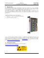
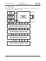
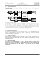

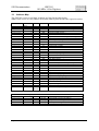
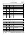

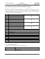

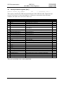
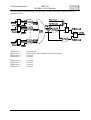


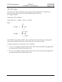


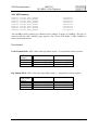
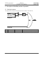

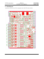
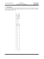
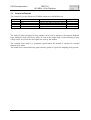

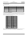
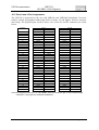
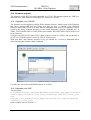


![[DRAFT] DEMO908JL16 User`s Manual](http://vs1.manualzilla.com/store/data/005639706_1-2a84cd2ce2f0b318fdb7aae7896f2a79-150x150.png)