1
INTEGRATED CIRCUITS
APPLICATION NOTE
AN10146-02
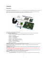
I2C 2002-1A EVALUATION BOARD
LM75A, PCA9501, PCA9515, PCA9543, PCA9550, PCA9551, PCA9554,
PCA9555, PCA9561, PCF8582C-2, P82B96
Abstract – Philips Semiconductors families of I2C devices are detailed in this application note that discusses
evaluation board set up and operation including typical applications.
Jean-Marc Irazabal - PCA Technical Marketing Manager
Steve Blozis - PCA International Product Manager
Phil Tracy - Engineering Manager
Specialty Logic Product Line
Logic Product Group
Philips Semiconductors
26 February, 2003
TABLE OF CONTENTS
OVERVIEW .......................................................................................................................................................................3
DESCRIPTION .....................................................................................................................................................................3
ORDERING INFORMATION..................................................................................................................................................4
I²C COMMUNICATION BASICS ...................................................................................................................................5
I2C 2002-1A KIT INFORMATION..................................................................................................................................7
BLOCK DIAGRAM ..............................................................................................................................................................7
I2C 2002-1A EVALUATION BOARD ..................................................................................................................................8
I2C 2002-1A EVALUATION BOARD ..................................................................................................................................8
I2C ADDRESSES AND BUSES ..............................................................................................................................................8
I2CPORT V2 ADAPTER CARD ..........................................................................................................................................9
OPERATIONS INSTRUCTIONS ..................................................................................................................................11
STARTING THE SOFTWARE – QUICK OVERVIEW ..............................................................................................................11
BEFORE STARTING ..........................................................................................................................................................14
PCA9501 ........................................................................................................................................................................15
PCA9515 ........................................................................................................................................................................18
PCA9543 ........................................................................................................................................................................19
PCA9550/PCA9551 .......................................................................................................................................................23
PCA9554 ........................................................................................................................................................................27
PCA9555 ........................................................................................................................................................................30
PCA9561 ........................................................................................................................................................................32
PCF8582C-2...................................................................................................................................................................37
P82B96 ...........................................................................................................................................................................39
LM75A ...........................................................................................................................................................................44
FREQUENTLY ASKED QUESTIONS .........................................................................................................................46
ADDITIONAL INFORMATION ...................................................................................................................................47
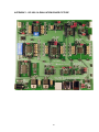
APPENDIX 1 - I2C 2002-1A EVALUATION BOARD BILL OF MATERIAL.........................................................48
APPENDIX 2 - I2C 2002-1A EVALUATION BOARD PICTURE .............................................................................49
2
OVERVIEW
Description
The I2C 2002-1A Evaluation Board is a low cost I2C based platform that allows Field Application Engineers, designers
and educators to use their Personal Computer (PC) to easily test and demonstrate new I2C devices in a platform that
allows multiple operations to be performed in a setting similar to a real system environment.
The I2C 2002-1A Evaluation Board Kit includes:
• I2C 2002-1A Evaluation Board – 5” x 5” 2 layer printed circuit board featuring 11 different I2C slave devices:
LM75A – Temperature Sensor
PCA9501 – 8-bit I/O Expander with 2Kbit serial EEPROM, Interrupt and 6 address pins
PCA9515 – I2C Repeater
PCA9543 – 4 Channel I2C Switch
PCA9550 – 2-bit LED Blinker
PCA9551 – 8-bit LED Blinker
PCA9554 – 8-bit I/O Expander with Interrupt
PCA9555 – 16-bit I/O Expander with Interrupt
PCA9561 – 6-bit I2C DIP Switch
PCF8582C-2 – 2Kbit serial EEPROM
P82B96 – I2C Bus Buffer
• I2CPORT v2 Adapter Card - plugs into the PC parallel port of the PC and provides the interface between the PC (bus
master) and the I2C bus slaves on the evaluation board at speeds over 100 kHz.
• 4-wire Connection Cable - connects the I2CPORT v2 Adapter Card with the I2C 2002-1A Evaluation Board at
normal SDA/SCL signal levels.
• USB adapter card – Connects the I2CPORT v2 Adapter Card with the Evaluation Board through an USB cable (cable
not included) via the P82B96.
NOTE: This is not a normal USB connection; the USB cable and USB connectors are used as the means to carry
the SCL/SDA signals at the special P82B96 voltage levels.
• 9 V Power supply - provides power to the evaluation board devices and LEDs. Operates from 100 to 240 volts at 47 to
66 Hz, AC Edison plug on one side and 9 volt DC mini-plug on the other side.
• CD-ROM – contains operating instructions and Win-I2CNT software
• Operating Instructions – detailed application notes, software operating instructions and set up procedures.
3
• Win-I2CNT (32-bit) - application software that provides the device specific and universal mode graphical
interface between the PC and I2CPORT v2 Adapter Card to control the I2C bus slaves featured on the I2C
2002-1A Evaluation Board. Compatible with Windows 95/98/ME/2000/NT and XP operating systems.
The devices used on the evaluation board are representative of the various general purpose I2C product families being
introduced by Philips. They were selected for these following reasons:
• PCA9501 - To show the programming difference between the PCF8574 8-bit GPIO (of which the PCA9501 has
the same state machine) and the PCA9554 8-bit GPIO (more complex state machine) and to showcase this new
device, that has both the PCF8574 GPIO and PCF8582C-2 2Kbit serial EEPROM contained in the same
package, with 6 address pins that allow up to 64 identical devices on the same bus.
• PCA9561 - To show its use as a 6-bit DIP switch replacement.
• PCA9543 - To show its use as a 2 channel multiplexer/switch.
• PCA9554/55 - To show how I/O expanders can be used as LED drivers, how they can be used to provide input
and output to the bus master and to show the size comparison of the PCA9555 in three different packages: The
large Surface Mount (SOIC - D), the smaller Thin Small Surface Package (TSSOP - PW) and the very small
Heat Sink Very Thin Quad Flat Pack No Leads (HVQFN - BS).
• PCA9550/51 - To show how the LED Blinkers are used to blink LEDs and to show how unused bits can be
utilized as general purpose inputs and outputs.
• PCF8582C-2 - To show 2Kbit EEPROMs and have two identical devices to multiplex with the PCA9543.
• LM75A - To show temperature sensors and have two identical devices to multiplex with the PCA9543.
• PCA9515 and P82B96 - To show that I2C bus expanders allow larger loading on the I2C bus and to be able to
connect a second card to the first evaluation board and to show how the P82B96 can be used to send both I2C
clock and data signals and power supply over USB cables or telephone wires.
Caution:
1. The USB connectors are NOT running USB signals; they are just used as a convenient hardware
wiring system. NEVER connect to a PC's USB port.
2. NEVER connect the telephone wires to your home telephone jack. They are just a convenient
hardware wiring system to communicate from one evaluation board to another.
Some of the experiments and demonstrations that can be performed using the I2C 2002-1A Evaluation Board include:
• Program and Blink LEDs using the GPIOs and/or the LED Blinker devices
o Learn differences in programming and blinking LEDs using the older and newer GPIO and the 2/8-bit
LED Blinkers.
o See the LED Blinker continue to blink LEDs when the I2C bus is disconnected.
• Command temperature sensors and 2K EEPROMs with same and different addresses through the
PCA9543 two channel switch used as a multiplexer and for voltage translation between 3.3 and 5V
o Learn how the multiplexer, 2Kbit serial EEPROM and temperature sensor work.
o See what happens when the master sends commands to devices with the same address at the same time.
o See the temperature sensor response at different voltage levels.
• Program the Multiplexed I2C EEPROM as a DIP switch replacement
Ordering Information
The complete I2C 2002-1A Evaluation Board Kit consists of the:
• I2C 2002-1A Evaluation Board
• I2CPORT v2 Adapter Card for PC parallel port
• 4-wire connector cable
• USB Adapter Card
• 9 V power supply
• CD-ROM with operating instructions and Win-I2CNT software
Purchase the I2C 2002-1A Evaluation Board Kit at www.demoboard.com
4
I²C COMMUNICATION BASICS
•
General Characteristics
The I²C protocol allows data to be transferred between devices using two open-drain (or open-collector) bidirectional lines. One line is the serial clock (SCL) and the other is the serial data (SDA). The bus master generates
the Start conditions, the clock signals on SCL, as well as the Stop condition. An Acknowledge is transmitted on the
bus after each byte is sent over the bus.
•
Bit Transfer
Information is transferred on an 8-bit word basis, Most Significant Bit (MSB) first.
- Device Address + Read/Write bit: specify which device is addressed (7 bits) and what type of operation needs
to be performed
- Control register: The data can sometimes be used by specific chips as an extension of the address (pointer
information) or be specific commands that prepare chips for further data bytes.
- Data.
I2C protocol for information transfer on the I2C bus, carried by the SDA line, specifies:
- Signal level must not change whenever SCL is High
- Level changes only when SCL is Low
- No restriction on the number of bytes sent during the same communication
Start and Stop conditions are special exceptions to these rules.
A Start condition is signaled by a High-Low transition of SDA while SCL is high.
A Stop condition is signaled by a Low-High transition of SDA while SCL is high.
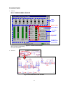
The figures below explain the different types of I²C transfer.
Blue: commands and data sent by the master
Yellow: data sent by the addressed slave.
1.
Write to a Slave device
S
ADDRESS
W
“0” = Write
A
DATA
A
DATA
A
P
Each byte is acknowledged by the slave device
The master is a MASTER-TRANSMITTER: It transmits both Clock and Data during the communication
2.
Read from a Slave device
S
ADDRESS
R
“1” = Read
A
DATA
A
DATA
A
P
Each byte is acknowledged by the master device
(except the last one, just before the STOP condition)
Acknowledged by the slave device
The master is a MASTER-TRANSMITTER and then a MASTER-RECEIVER:
- It transmits the Clock all the time
- It sends the Slave Address data and then becomes a receiver
The address byte is acknowledged by the slave device, and then received data is acknowledged by the master.
When the final byte is received the master generates a "not acknowledge,” followed by a Stop."
5
3.
Combined Write and Read
S
ADDRESS
W
A
A
Sr
ADDRESS
Each byte is
acknowledged
by the slave
Re-Start
device
“0” = Write
4.
DATA
ADDRESS
R
“1” = Read
DATA
A
DATA
A
P
Each byte is acknowledged
by the master device
(except the last one, just
before the STOP condition)
Acknowledged by the slave device
A
DATA
A
DATA
A
Sr
ADDRESS
Each byte is acknowledged
by the master device
(except the last one, just
before the STOP condition)
Acknowledged by the slave device
W
“0” = Write
A
DATA
A
Each byte is
acknowledged
by the slave
device
Re-Start
Start and Stop Conditions
- A Start Condition (S) is a High To Low Transition on SDA line when SCL is High
- A Stop Command (P) is a Low To High Transition on SDA line when SCL is High
S
•
A
“1” = Read
Combined Read and Write
S
•
R
P
Acknowledge
Acknowledge is done by the receiver (master or slave) on the 9th pulse (on the HIGH period), after each byte has
been received.
- The Transmitter releases the bus SDA line goes High
- The Receiver pulls down the bus SDA line goes Low
No acknowledge
Acknowledge
6
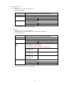
P
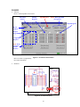
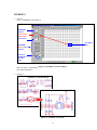
I2C 2002-1A KIT INFORMATION
Block Diagram
I2C 2002-1A Evaluation kit includes the following:
1.
2.
3.
4.
5.
6.
7.
I2CPORT v2 Adapter Card
Win-I2CNT software (CD-ROM)
9 V power Supply
4-pin I2C cable
I2C 2002-1A Evaluation board
USB Adapter Card
Operating instructions (CD-ROM)
CD - ROM
PC -Win95/98/2000/NT/XP
I2C 2002-1A
Evaluation Kit
Parallel Port
I2CPORT v2
Adapter Card
Win-I2CNT
Software
I2C Cable
I2C Cable
USB
Adapter
Card
USB Cable
9V
Power
Supply
I2C 2002-1A Evaluation Board
I2C Cable
9V
Power
Supply
I2C 2002-1A Evaluation Board
Figure 1. Hardware and Software Schematic
The second evaluation board and power supply is only provided to FAEs.
7
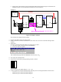
USB Cable
or
Phone Cable
I2C 2002-1A Evaluation Board
I2C 2002-1A Evaluation Board
Main I2C Bus
SCL/SDA
1
1
PCA9550
PCA9551
PCA9554
PCA9543
PCA9555
PCA9561
PCA9501
PCF8582
LM75A
LM75A
P82B96
PCA9515
SCL0/SDA0
2
SCL3/SDA3
SCL1/SDA1
4
9V
SCL2/SDA2
3.3 V
REGULATORS
5.0 V
RJ11
3
USB A
3
USB B
3
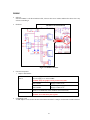
Figure 2. I2C 2002-1A Evaluation board block diagram
6 different types of connections are available on the evaluation board:
1. I2C 4-wire connector (unbuffered). To be connected to the I2CPORT v2 Adapter Card or to another I2C evaluation
board.
2. I2C 4-wire connector (buffered). Using a buffered PCA9515 connection, to be connected to the I2CPORT v2
Adapter Card or to another I2C evaluation board.
3. RJ11 phone line or USB port A or USB port B. Using a buffered P82B96 connection, to connect to the I2CPORT
v2 Adapter Card through the USB Adapter Card or to another I2C evaluation board. It connects via the I2C 4-wire
connector to a P82B96 demo board (master) and then via any standard USB cable (not supplied) to the I2C
evaluation board. It is also possible to directly link from one I2C evaluation board to another. The RJ11 connector is
used to send the I2C signals through a normal 4-core telephone wire. USB port A or B connect the I2C signals
through USB cables. All these connectors also allow transfer of the 5.0 V or 9.0 V power supply.
9 V Power Supply. Input via a 3.5 mm mini plug.
I2C Addresses and Buses
Device Type
PCA9501
PCA9543
PCA9550
PCA9551
PCA9554
PCA9555
PCA9561
PCF8582C-2
LM75A – 1
LM75A – 2
PCA9515
P82B96
I2C Address
B0
30
E4
C0
CC
40
4C
98
A0
90
92
None
None
Description
2 Kbit EEPROM
8-bit I/O Expander
2 Channel I2C Multiplexer
2-bit LED Blinker
8-bit LED Blinker
8-bit I/O Expander
16-bit I/O Expander
6-bit I2C DIP Switch
2 Kbit EEPROM
Temperature Sensor
Temperature Sensor
I2C Repeater
Bi-Directional I2C Bus Buffer
Table 1. Device addresses and buses
8
I2C Bus
SCL1/SDA1 (Channel 0 PCA9543)
SCL/SDA (Main bus)
SCL/SDA (Main bus)
SCL/SDA (Main bus)
SCL/SDA (Main bus)
SCL/SDA (Main bus)
SCL/SDA (Main bus)
SCL2/SDA2 (Channel 1 PCA9543)
SCL1/SDA1 (Channel 0 PCA9543)
SCL2/SDA2 (Channel 1 PCA9543)
SCL/SDA ↔ SCL0/SDA0
SCL/SDA ↔ SCL3/SDA3
I2CPORT v2 Adapter Card
The I2CPORT v2 Adapter Card connects to the standard DB-25 parallel port found on IBM-compatible PCs and
provides bi-directional communication with I²C devices via the I²C protocol. The adapter card can be powered from the
PC's parallel port or externally powered from the I²C target card to support 3.3 V and 5.0 V applications. The LED
indicates the presence of power (steady) and activity on the I²C data line (blinking or dimming, depending on the
selected bus speed).
The I2CPORT v2 Adapter Card can be used stand-alone, since it obtains 5 V power from the PC parallel port. This
allows the on-board I2C 256-byte EEPROM to be programmed and verified without the need for an external power
source. When the I2CPORT v2 Adapter Card is connected to other I²C target systems, then 5 V power should be
supplied from the target to the Adapter Card via one of the three 4-pin headers on the Adapter.
Caution: All three of the 4-pin headers are pinned differently!
The LED will indicate a proper power connection and activity of the SDA line. You may not see the LED blink
depending upon the bus speed selected. It should be noted that if you are deriving power from the computer’s parallel
port, the LED might not turn on until the software is started.
The I²C-bus voltage for the target system is determined by the setting of JP2:
Open = 3.3 V I²C; Closed = 5 V I²C.
I2C 2Kbit EEPROM
To the PC parallel
port
To the I2C Evaluation Board
I2C bus signals
Jumper JP2 I2C Voltage Selection (Bus voltage)
Open
= 3.3 V bus
Closed = 5.0 V bus
Figure 3. I2CPORT v2 Adapter Card
•
Jumpers
When connecting the I2CPORT v2 Adapter Card to an I²C target, the target system supplies 5 V power via one of
the three 4-pin I²C headers. Jumper JP2 selects the pull-up voltage for the I²C target and the I2CPORT v2 Adapter
Card.
JP2 OPEN
JP2 CLOSED
3.3 V I²C pull-up voltage (through 4.7 kΩ resistors)
5.0 V I²C pull-up voltage (through 4.7 kΩ resistors)
In the event your target system only has 3.3 V power available, try closing JP2 and supplying 3.3 V power from the
target via the 4-pin header. In this configuration, the on-board regulator is bypassed. I2C bus pull-up resistors to 3.3
V can be added on your target board if the I2C bus pull-up voltage through the adapter card is too low (diode drop
through the adapter).
•
On-board EEPROM
9
The on-board 8-pin DIP socket U2 supports I²C communication with the included 256-byte (2 Kbit) EEPROM or
other EEPROM devices that allow pin 7 to be floating. The default I²C address for this EEPROM socket is (0xAE),
allowing other I²C EEPROM devices sharing this pinout and address, to be accessed. Several supported EEPROM
types are listed in the "Device Menu" of the Win-I2CNT software package. This EEPROM allows verification of
hardware and software functionality as well as the ability to program EEPROM devices using only the computer and
the I2CPORT v2 Adapter Card.
Caution: If an external I²C device is connected to the Adapter Card, which uses this same I²C address
(0xAE), the EEPROM in socket U2 should be removed to avoid address conflicts.
•
I²C Connectors
The I2CPORT v2 Adapter Card includes three four-pin headers for connecting I²C to external devices or target
systems; these are pinned differently to allow compatibility with legacy I²C connections in existing evaluation
boards and development systems from Philips and other suppliers.
Caution:
1. Use extreme care to use the correct pin configuration, as all three are different! Inadvertent
power/ground reversal may damage the Adapter and/or your target system.
2. Note that the connector referenced JP3 must be used to communicate with the I2C 2002-1A evaluation
board. Pinout is as following (from top to bottom): Vcc, GND, SCL, SDA.
When an external I²C peripheral is connected to the I2CPORT v2 Adapter Card, the 5 V power should be supplied
by the target board or an external power supply through the four-pin header connectors on the adapter. In this
configuration, Schottky steering diodes prevent interference between external 5 V supply and the power supplied to
the adapter by the computer’s parallel port. A 3 V power source may also work if the jumper JP2 on the Adapter
Card is closed (see Jumper Settings above).
Note: the LED may indicate power to the Win-I2CNT Adapter even though the connected I²C target board is
unpowered, (power is also supplied by the parallel port when the PC is active).
10
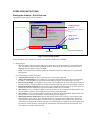
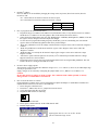
OPERATIONS INSTRUCTIONS
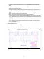
Starting the Software – Quick Overview
Starting the program will open the main window.
Working Window
Selection
Universal modes
Open the device specific
screen
Mode selector
I2C clock (SCL)
indicator
Message Panel
Help Hints
Parallel Port Indicator
Figure 4. Software Main Window
All the information can be found in the software’s user manual available on the CD-ROM.
•
Message Panel:
1. When opening the software: indicates that the port adapter has been found and that I2C communications can
start. If a problem is detected when opening the software, the message “Win-I2C hardware not detected” is
displayed Action required: check port adapter
2. During I2C communications: indicates whether the communication has been done properly or a problem has
been detected.
List of the messages available in the panel:
Transmission successful - the last I²C transmission was successfully completed.
Address not acknowledged - an I²C address was successfully transmitted but no slave device acknowledged
the address. A STOP condition is sent after the acknowledge clock pulse if no acknowledge is received.
Data not acknowledged - an I²C address was previously acknowledged but one of the following data bytes was
not acknowledged. . A STOP condition is sent after the acknowledge clock pulse if no acknowledge is received.
Read acknowledged corrupted - the master tried to send a NACK (no acknowledge) for the last read byte in a
transmission, but it was corrupted by a low level on SDA by another device on the bus.
SDA stuck low - before a START condition is initiated, the software verifies that both the SDA and SCL lines
are high. If SDA is stuck low, then an SDA stuck low message will be displayed.
SCL stuck low - before a START condition is initiated, the software verifies that both the SDA and SCL lines
are high. If SCL is stuck low, then an SCL stuck low message will be displayed.
Win-I2CNT hardware not detected- when the Win-I2CNT software is first started, it verifies that the WinI2CNT hardware exists at LPT1. If it is not found at LPT1, it will check LPT2, and then LPT3. Detection is
terminated when Win-I2CNT hardware is found. The user may manually select a different port from the one
selected by the program but Win-I2CNT will again verify that hardware is available at the selected parallel port.
The software will not attempt to proceed with any transmissions until the hardware has been detected. Autowrite settings are cleared to Auto Write Off.
11
•
I2C Frequency Indicator:
Indicates the current clock frequency used during the transmissions. Accessing the Options menu can change this
value.
Options I2C Frequency will open a window allowing a new clock frequency to be programmed. Note that the
frequency information will be stored in the Registry and will be recalled when the program restarts at a later time.
Maximum available clock frequency is PC dependent. Bit rates up to 70 kHz can be expected on a 66 MHz 486
class computer and possibly over 100 kHz with a Pentium class computer. However, many factors influence the
maximum bit rate and results may vary significantly.
•
Mode Indicator:
The Mode Indicator shows the present state of the parallel port kernel-mode driver. ‘Normal’ access provides higher
performance access to the parallel port, but may fail if the port is already in use by another kernel-mode driver.
While slower, ‘Slow’ access provides more reliable access to ports that have already been opened by another kernelmode driver. If the driver fails while in ‘Normal’ access mode, a ‘Privileged Instruction’ error may be encountered
and it is recommended to keep the driver in ‘Slow’ mode on that computer. Mode change is done through the
Options menu.
Options
Normal access Normal Mode selected
Options Normal access
Slow Mode selected
•
Help Hints:
The main screen contains a panel at the bottom that gives a short description of the item the cursor is currently
above. Almost all buttons, boxes, and other controls have these hints when moving the cursor around the screen with
the mouse.
•
Parallel Port Indicator:
The main screen has an area in the bottom right hand part of the screen that shows the active parallel port. This port
can be changed by selecting a different port from the Options menu. This box is empty if no hardware has been
found.
•
Working screen (Device Specific, Universal Transmitter/receiver and User Definable) can be selected under the
Devices menu.
1.
Device Specific menu.
Devices supported by Win-I2CNT are listed below.
Cells in Yellow represent devices mounted on the I2C 2002-1A Evaluation board.
DEVICE CATEGORY
Clock Buffers
Real Time Clocks
EEPROM
DEVICE NAME
PCK2001
PCK2001M
PCF8583
PCF8593
16x8
128 bit
128x8
1K
256x8
2K
512x8
4K
1Kx8
8K
2Kx8
16K
4Kx8
32K
8Kx8
64K
16Kx8
128K
32Kx8
256K
64Kx8
512K
12
DEVICE CATEGORY
I/O Expanders
LED Drivers/Blinkers
Multiplexers/Switches
DIP Switch
Static RAM
Tone Generator
Thermal Management
2.
DEVICE NAME
PCA9554
PCA9554A
PCA9555
PCA9556
PCA9557
PCA9558
PCF8574
PCF8574A
PCF8575
PCA9500
PCA9501
PCA9550
PCA9551
PCA9552
PCA9553
SAA1064
PCA9540
PCA9542
PCA9543
PCA9544
PCA9545
PCA9546
PCA9548
PCA8550
PCA9559
PCA9560
PCA9561
PCF8570
PCD3311/PCD3312
LM75A
NE1617A
NE1618
NE1619
Universal Transmitter/Receiver Menu (Under Devices Universal Modes)
This screen allows writing up to 5 different fully programmable messages.
Commands
Programming
I2C sequencing
parameters
Send selected
message
Sequence programming
Programmable delay between the messages
Figure 5. Universal Transceiver / Receiver Window
13
Characteristics and tips for the Universal Transmitter/Receiver screen:
- Length of the messages is variable but limited to 16 data instructions maximum
- 5 different messages can be programmed
- First START and STOP instructions can not be removed
- I2C Re-Start Command “S” key
- A restart condition may be inserted into any Message location by pressing the “S “ key on your keyboard. The
software deletes the boxes after the repeated start condition and then inserts 'S 00 W FF'. Only one Restart per
message is allowed.
- I2C Write Command “W” key
This may be changed to a Read condition by pressing the ‘R“ key.
- I2C Read Command “R” key
This may be changed to a Write condition by pressing the ‘W’ key.
- Add an Instruction “INSERT” key
Pressing this key adds an extra edit box to the Message. The maximum number of data bytes is 16, so the
INSERT key will be ignored if there are already 16 bytes present.
- Remove an Instruction “DELETE” key
Pressing this key deletes the data byte where the cursor is current located. The software requires that you keep
at least one data byte in the Message. It will also not let you delete the address byte or R/W bit following a
restart. If you want to delete a restart, make sure the cursor is in the Start box and then press the DELETE key.
- Data: 0 to 9 and A to F keys. Others keys are not allowed
3.
•
User Definable Device (Under Devices Universal Modes
The User Definable Device allows defining a customized I²C device and then enables the user to change the
values of the individual cells within the grid using various controls such as sliders and spin controls. Additional
information can be found in the software’s user manual.
Acknowledge:
Normally, the software checks the acknowledge bit, after every byte written, to ensure that the slave-receiver has
pulled the SDA line low. When the Ignore Acknowledge item is checked in the Options menu, the software ignores
the acknowledge bit state during writes, so it is important to note that the user will not have any feedback whether or
not a device is actually receiving the message.
Options
Ignore Acknowledge Acknowledge cycle is ignored
Options Ignore Acknowledge
Acknowledge is performed
Before Starting
When the buffer chip P82B96 is active on the main I2C bus (SDA/SCL), it repeats the bus signals onto the buffered bus
at the USB and phone connectors. Propagation delays in the chip mean that when the SDA/SCL lines are released, they
cannot fully rise until after the buffered bus rises. So propagation delays in P82B96 cause the 300 ns “step” observed in
the bus rise time waveforms. This step will lengthen when long cables are plugged into the buffered bus connectors.
If these effects disturb any oscilloscope measurements, they may be eliminated by simply removing power to the
P82B96 so it has no effect on the main bus: simply remove JP173, or both jumpers JP171 and JP172 to eliminate the
steps in the waveforms.
14
PCA9501
•
Software
Device I/O Expanders
PCA9501
GPIO register value
GPIO value
GPIO Read / Write
Options
GPIO
programming
GPIO address
EEPROM address
Selected byte
information
Write Time
Auto Write
Feature
Byte 8BH or
13910
EEPROM
Read / Write
Options
Set the all
EEPROM to
the same
value
EEPROM
programming
Figure 6. PCA9501 Control Window
Blue: accessible to programming
Red: status information
•
I2C2002-1A Evaluation Board
Hardware
Figure 7. PCA9501 Schematic
15
•
External Components
1. LD60 to LD67: Used to visualize I/O signals
2. Jumpers and Headers:
JP6
JP60 and JP61
JP69
JP610 to 615
LJP60 to LJP67
•
Used to measure the current flowing through VDD.
Must be CLOSED under other conditions (no measurement)
Headers to monitor the pins of the PCA9501
Used to program the /WC pin (Write Control)
JP69 CLOSED
Write to the EEPROM allowed
JP69 OPEN
Write to the EEPROM not allowed
Used to control the 6 programmable address pins
JP610, JP611, JP612 or
A0, A1, A2 or A5 is connected to GND
615 CLOSED
(Low logic Level)
JP610, JP611, JP612 or
A0, A1, A2 or A5 is connected to VDD
615 OPEN
(High logic Level)
JP613 or 614 CLOSED
A3 or A4 is connected to VDD
(High logic Level)
JP613 or 614 OPEN
A3 or A4 is connected to GND
(Low logic Level)
Used to disconnect the default output stage (LED + Resistor) in order to
connect an external hardware
LJP6x CLOSED
LD6x and DR6x connected to IOx
LJP6x OPEN
LD6x and DR6x disconnected from IOx
Default I2C address
Note: I2C address can be modified by changing the voltage values on pins A0 to A5 (JP610 to JP615) with:
- Ax = 1 when JP61x is open
- Ax = 0 when JP61x is closed
PCA9501 GPIOs (U6)
PCA9501 EEPROM (U6)
•
Binary
0011000
1011000
Hexadecimal
30
B0
How to program the PCA9501’s GPIOs
Important note before starting experiments on the PCA9501:
The device is not on the main I2C bus (bus from the Adapter Card) but on PCA9543’s downstream channel 0.
To access the PCA9501, PCA9543 must be configured with its upstream channel connected to Channel 0.
For more information about how to program the PCA9543, please refer to the section “PCA9543”, paragraph
“How to access the downstream devices”.
1.
2.
3.
4.
5.
Program the device I2C address in the I/O expander address box (Hexadecimal value). Verify that the software
I2C address and the device I2C address are the same (jumpers JP610 to JP615)
Check (Light Green) (“1”) or uncheck (Dark Green) (“0”) the I/O boxes
“Write” pushbutton to force the I/Os
“Read” pushbutton to read the I/O state
“Auto Write” option: when the option is ON (Green), an I2C command is performed each time a change
happens in the device control window
16
ADDRESS ACK DATA ACK
GPIO state change
Figure 8. PCA9501’s GPIO programming
•
How to program the PCA9501’s EEPROM
Important note before starting experiments on the PCA9501:
The device is not in the main I2C bus (bus from the port adapter) but on PCA9543’s downstream channel 0.
To access the PCA9501, PCA9543 must be configured with its upstream channel connected to Channel 0.
For more information about how to program the PCA9543, please refer to the section “PCA9543”, paragraph
“How to access the downstream devices”.
The table shows the 256 bytes that can be programmed. Two one-digit hexadecimal numbers H1H0 with H1 being
the line number and H1 being the column number that define each byte.
Example: Byte 6E is located at the intersection of line 6 with column E.
1.
2.
3.
4.
5.
6.
Program the device I2C address in the EEPROM address box (Hexadecimal value). Verify that the software I2C
address and the device I2C address are the same (jumpers JP610 to JP615)
Verify that EEPROM writing is allowed. Pin WC must be connected to Logic Level Low. This is performed by
closing the jumper JP69.
Write Operation (once WC is at Logic Level Low):
The EEPROM can be programmed:
- Byte after byte (“Write Byte” pushbutton): The byte where the cursor is will be programmed.
- Entirely in one automatic sequence (“Write All” pushbutton)
Read Operation:
The EEPROM can be read:
- Byte after byte (“Read Byte” pushbutton) : The byte where the cursor is will be read.
- Entirely in one automatic sequence (“Read All” pushbutton): The byte where the cursor is will be read.
Write Time feature: define the waiting time between 2 write accesses (8-byte write operation) in order to let the
EEPROM perform its E/W cycle. Use the Up and Down arrows to change the value.
Preset feature: Program all the EEPROM bytes with the same value (value in the box) when “Set Data” button
is pushed
17
PCA9515
•
Software
Since the PCA9515 is a bus repeater, it doesn’t have an I2C address and therefore doesn’t have any software
controlling it.
•
Hardware
I2C2002-1A Evaluation
B d
•
Figure 9. PCA9515 Schematic
External Components
1. Jumpers and Headers:
JP4
JP40
JP41 and JP42
•
Used to measure the current flowing through VDD
Must be CLOSED under other conditions (no measurement)
Used to control the EN (Enable) pin
JP40 CLOSED
PCA9515 is enabled
JP40 OPEN
PCA9515 is disabled
Headers to monitor the pins of the PCA9515
Application example
PCA9515 (U4) can be used to interface with another card (e.g. second I2C 2002-1AEvaluation board) in order to
keep the main I2C bus load identical in the 2 cards. Check that JP40 in Board 1 is closed for such application.
PC
2
I C connector
PCA
9515
Board 1
PCA
9515
I2C connector
Board 2
Figure 9. PCA9515 Application Example
Caution:
1. P82B96 cannot drive the PCA9515. So it is not possible to exercise the PCA9515 buffered output header
(SCL0/SDA0) when theP82B96 is generating the main bus signals, for example when phone wire or USB
connections (SCL3/SDA3). P82B96 in series with PCA9515 is not allowed.
2. Don't link PCA915 output bus SDA0/SCL0 to the corresponding SDA0/SCL0 header of PCA915 on a
second board. Be sure to make this connection to SDA/SCL on the second board as shown in Fig. 9.
18
PCA9543
•
Software
Device Multiplexers/Switches
PCA9543
Figure 7. PCA9543 Control Window
Device address
Control
Register Value
Read / Write
Operation
Channel
Selection
Interrupt
Status
Auto Write
Feature
Figure 10. PCA9543 Control Window
Blue: accessible to programming
Red: status information
•
Hardware
I2C2002-1A Evaluation Board
`
Figure 11. PCA9543 Schematic
19
•
External Components
1. Jumpers and Headers:
JP3
JP30 and JP32
JP31
JP33 and JP36
JP34 and JP35
Used to measure the current flowing through VDD
Must be CLOSED under other conditions (no measurement)
Headers to monitor the pins of the PCA9543 (except VDD and GND)
Used to control the programmable address pin A0
JP31 CLOSED
A0 is connected to GND (Low logic Level)
JP31 OPEN
A0 is connected to VDD (High logic Level)
Used to Control the pull-up voltage value on SDA2/SCL2
Caution: JP33 and JP36 MUST NOT to be CLOSED at the same time
JP33 CLOSED AND
SDA2/SCL2 at 3.3 V
JP36 OPEN
JP33 OPEN AND
SDA2/SCL2 at 5.0 V
JP36 CLOSED
Used to Control the pull-up voltage value on SDA1/SCL1
Caution: JP34 and JP35 MUST NOT to be CLOSED at the same time
JP34 CLOSED AND
SDA1/SCL1 at 3.3 V
JP35 OPEN
JP34 OPEN AND
SDA1/SCL1 at 5.0 V
JP35 CLOSED
Note: The two buses can be at the same or different voltage levels.
2.
3.
4.
5.
•
RESET pushbutton: Used to reset the PCA9543 (all channels deselected)
LD120: Used to visualize Interrupt on /INT0.
- LED OFF = No interrupt (/INT0 pin high)
- LED ON = Interrupt (/INT0 pin low)
LD130: Used to visualize Interrupt on /INT1.
- LED OFF = No interrupt (/INT1 pin high)
- LED ON = Interrupt (/INT1 pin low)
LD140: Used to visualize Interrupt on /INT.
- LED OFF = No interrupt (/INT pin high)
- LED ON = Interrupt (/INT pin low)
Default I2C address
Note: I2C address can be modified by changing the voltage values on pin A0 (JP31) with:
- A0 = 1 when JP31 is open
- A0= 0 when JP31 is closed
PCA9543 (U3)
•
Binary
1110010
Hexadecimal
E4
How to program the PCA9543
1. Program the device I2C address in the address box (Hexadecimal value). Verify that the software I2C address
and the device I2C address are the same (jumper JP31)
2. Check ( ) (connected to the upstream channel) or uncheck (not connected to the upstream channel) the
channel(s)
3. “Write” pushbutton to write in the PCA9543 Control register
4. “Read” pushbutton to read the PCA9543 Control register
5. Interrupts: Read only data. When Dark Green color is displayed, an Interrupt has been detected in the
corresponding input (Interrupt input is low and by consequence the PCA9543 Interrupt Output is also low).
Interrupts are generated by either the PCA9501 or the PCA9554.
- When PCA9501 generates an Interrupt (Logic level Low), LD120 is ON.
20
6.
7.
- When PCA9554 generates and Interrupt (Logic level Low), LD130 is ON
- When PCA9543 Interrupt output is low, LD140 is ON.
“Auto Write” option: when the option is ON (Green), an I2C command is performed each time a change
happens in the device control window
PCA9543 Reset: The user can reset The PCA9543 by using the PB0 pushbutton. This will initialize the device
causing all the downstream channels to be disconnected.
•
How to access the downstream devices
- Downstream channel 0 only – Access to PCA9501 and LM75A_0 :
When PCA9501 and LM75A_0 devices only need to be accessed, execute the following sequence:
1. Device Multiplexers/Switches PCA9543
2. Verify that Device Address = E4H or change the PCA9543software’s I2C address in order to match the
programmed I2C address in the evaluation board (see state of JP31)
3. Check( ) channel 0 – “X1” is displayed (with X = 0, 1 or 2 or 3)
4. Push “Write” pushbutton
5. “Transmission Successful” is displayed
- Downstream channel 1 only – Access to PCF8582C-2 and LM75A_1:
When PCF8582C-2 and LM75A_1 devices only need to be accessed, execute the following sequence:
1. Device Multiplexers/Switches PCA9543
2. Verify that Device Address = E4H or change the PCA9543 software’s I2C address in order to match the
programmed I2C address in the evaluation board (see state of JP31)
3. Check( ) channel 1 – “X2” is displayed (with X = 0, 1 or 2 or 3)
4. Push “Write” pushbutton
5. “Transmission Successful” is displayed
- Downstream channel 0 and Channel 1- Access to PCA9501, PCF8582C-2, LM75A_0 and LM75A_1:
When the 2 channels need to be accessed at the same time, execute the following sequence:
When those devices need to be accessed, execute the following sequence:
1. Device Multiplexers/Switches PCA9543
2. Verify that Device Address = E4H or change the PCA9543 software’s I2C address in order to match the
programmed I2C address in the evaluation board (see state of JP31)
3. Check( ) channel 0 and channel 1 – “X3” is displayed (with X = 0, 1 or 2 or 3)
4. Push “Write” pushbutton
5. “Transmission Successful” is displayed
•
I2C downstream supply voltages
PCA9543 device is supplied by 3.3V. However, the 2 downstream channels can be supplied by either 3.3 V or 5 V.
This is done by configuring the jumpers JP33 to JP36 as explained in the jumper table above.
Caution:
JP33 and JP36 MUST NOT be closed at the same time.
JP34 and JP35 MUST NOT be closed at the same time.
The evaluation board could be partially or entirely damaged if this recommendation is not followed.
•
Add more I2C devices in the downstream channel(s)
Headers TP1 (SCL1/SDA1) and TP2 (SCL2/SDA2) allow easy plug of additional devices in each downstream
channel.
•
Programming example
The program below allows writing in either the PCF8582C-2 or the EEPROM in the PCA9501. In this example, we
set the 2 EEPROMs at the same I2C address (A0) and we use the PCA9543 to deconflict them.
1.
Initialization
- PCF8582C-2 I2C address must be A0 H (JP81, JP82 and JP83 must be closed)
- PCA9501 I2C address must be A0 H (JP610, JP611, JP612 and JP615 must be closed, JP613 and JP614
must be open)
- PCA9543 I2C address must be E4H (JP31 closed)
21
2.
Reset the PCA9543 by pushing the PB0 pushbutton (no downstream channel connected to the upstream
main channel)
Execute the following sequence:
Message 1 addresses the PCA9543 and connects the
upstream channel to downstream channel 0 (executed at the
STOP command)
Message 2 addresses the PCA9501 (connected to channel 0)
and writes several bytes
Message 3 addresses the PCA9543 and connects the
upstream channel to downstream channel 1 (executed at the
STOP command)
Message 4 addresses the PCF8582C-2 (connected to channel
1) and writes several bytes
The scope waveforms illustrate the communication described above.
Msg 1 Msg 2
Msg 3 Msg 4
SCL
Upstream Channel
SDA
SCL1
SDA1
PCA9501 receives the
communication
PCA9543’s Downstream
Channel 0
PCA9501 does not receive the
communication
Figure 12. PCA9543 programming waveforms
22
PCA9550/PCA9551
•
Software
Device LED Drivers/Blinkers
Device LED Drivers/Blinkers
PCA9550
PCA9551
LED
drivers
states
Register values
Device address
Auto Write
Feature
Read / Write
Operation
Frequencies
and duty cycles
programming
Figure 13. PCA9551 Control Window
Blue: accessible to programming
Red: status information
•
Hardware
I2C2002-1A Evaluation Board
Figure 14. PCA9550 and PCA9551 Schematic
23
•
External Components
A. PCA9550:
1. LD 20 and LD21: Used to visualize the I/Os
2. Jumpers and Headers:
JP2
JP20 and JP21
JP23
LJP20 and LJP21
3.
Used to measure the current flowing through VDD
Must be CLOSED under other conditions (no measurement)
Headers to monitor the pins of the PCA9550
Used to control the programmable address pin A0
JP23 CLOSED
A0 is connected to GND (Low logic Level)
JP23 OPEN
A0 is connected to VDD (High logic Level)
Used to disconnect the default output stage (LED + Resistor) in order to
connect an external hardware
LJP2x CLOSED
LD2x and DR2x connected to LEDx
LJP2x OPEN
LD2x and DR2x disconnected from LEDx
RESET pushbutton: Used to reset the PCA9550
B. PCA9551:
1. LD10 to LD17: Used to visualize the I/Os
2. Double DIP switch: Used to force High or Low logic levels I/O4 and I/O5
3. Jumpers and Headers:
JP1
JP10 and JP11
JP19
JPR1
JPR2
JPR3
LJP10 to LJP17
4.
Used to measure the current flowing through VDD
Must be CLOSED under other conditions (no measurement)
Headers to monitor the pins of the PCA9551
Used to control the programmable address pin A0
JP19 CLOSED
A0 is connected to GND (Low logic Level)
JP19 OPEN
A0 is connected to VDD (High logic Level)
Used to supply 2.5 V to the PCA9551
Used to supply 5.0 V to the PCA9551
Used to supply 3.3 V to the PCA9551
Caution: Only one jumper MUST BE CLOSED at a time
JPR1 CLOSED AND
PCA9551’s power supply is 2.5 V
JPR2 OPEN AND
JPR3 OPEN
JPR2 CLOSED AND
PCA9551’s power supply is 5.0 V
JPR1 OPEN AND
JPR3 OPEN
JPR3 CLOSED AND
PCA9551’s power supply is 3.3 V
JPR1 OPEN AND
JPR2 OPEN
Used to disconnect the default output stage (LED + Resistor) in order to
connect an external hardware
LJP1x CLOSED
LD1x and DR1x connected to LEDx
LJP1x OPEN
LD1x and DR1x disconnected from LEDx
RESET pushbutton: Used to reset the PCA9551
24
•
Default I2C address
Note: I2C address can be modified by changing the voltage values on pin A0 (JP23 for PCA9550, JP19 for
PCA9551) with:
- A0 = 1 when JP23 for PCA9550 or JP19 for PCA9551 is open
- A0= 0 when JP23 for PCA9550 or JP19 for PCA9551 is closed
PCA9550 (U2)
PCA9551 (U1)
Binary
1100000
1100110
Hexadecimal
C0
CC
•
How to program the PCA9550 and PCA9551
1. Program the device I2C address in the address box (Hexadecimal value). Verify that the software I2C address
and the device I2C address are the same (jumpers JP23 for PCA9550, JP19 for PCA9551)
2. Choose the desired LED output state: ON, OFF, Blinking Rate 1 (PWM0), Blinking Rate 2 (PWM1). Note that
the register value(s) change(s) when the output state changes.
3. Use the cursors to program the blinking frequency and the duty cycle for each blinking rate. Note that the
register values are automatically updated when cursor position changes.
4. “Write All” pushbutton to write the settings in the PCA9550/51. Register values can be read in the “Registers”
windows
5. “Read All” pushbutton to read all the PCA9550/51 register values. Register values can be read in the
“Registers” windows
6. “Read Input Reg” to read only the PCA9550/51 input register. Register value can be read in the “Input
Register” window
7. “Auto Write” option: when the option is ON (Green), an I2C command is performed each time a change
happens in the device control window
8. PCA9550/51 Reset: The user can reset The PCA9550 and PCA9551 by using the PB0 pushbutton. This will
initialize the device causing all the LEDs to be OFF.
•
PCA9551 Power supply options
The PCA9551 can be powered at three different voltages (2.5 V, 3.3 V and 5.0 V). However, the LED output stage
can only be powered at 5.0 V.
Supply voltages can be selected by configuring the jumpers JPR1 (2.5 V), JPR2 (5.0 V) or JPR3 (3.3 V)
Caution:
Be sure that ONLY one jumper is closed at a time. The evaluation board could be partially or entirely
damaged if this recommendation is not followed.
•
How to use the PCA9551 as a GPIO
Unused LED driver outputs can be used as General Purpose Inputs and Outputs. A double DIP switch has been
implemented in order to force PCA9551’s I/O4 and I/O5.
1. Power down the evaluation board
2. PCA9551 I2C address must be CCH, jumper JP19 must be closed
3. Verify that LJP14 and LJP15 are closed
4. Program the DIP switches as following:
ON
5.
6.
The 2 switches are then OFF
Power up the evaluation boards. All the LEDs must be OFF
Read the Input register
Input register value is 11111111b or FFH. All the
pins are read with a Logic Level 1
25
7.
Program the DIP switches as following:
ON
8.
I/O4 is now at Logic Level 0 and LD14 must be ON.
Read the Input register
Input Register value is now 11101111 or EFH.
I/O4 is read with a Logic Level 0
26
PCA9554
•
Software
Device I/O Expanders
Auto Write
Feature
PCA9554
Output
Register
Read / Write Operation
(all registers)
Device address
Configuration
Register
Input Register
Register
Programming
Polarity
Register
Read / Write
Operation
(specific register)
Figure 15. PCA9554 Control Window
Blue: accessible to programming
Red: status information
•
Hardware
I2C2002-1A Evaluation Board
Figure 16. PCA9554 Schematic
27
•
External Components
1. LD70 to LD77: Used to visualize I/O signals
2. Jumpers and Headers:
JP7
JP70 and JP71
JP78
LJP70 to LJP77
•
Used to measure the current flowing through VDD
Must be CLOSED under other conditions (no measurement)
Headers to monitor the pins of the PCA9554
Used to control the programmable address pin A0
JP78 CLOSED
A0 is connected to GND (Low logic Level)
JP78 OPEN
A0 is connected to VDD (High logic Level)
Used to disconnect the default output stage (LED + Resistor) in order to
connect an external hardware
LJP7x CLOSED
LD7x and DR7x connected to IOx
LJP7x OPEN
LD7x and DR7x disconnected from IOx
Default I2C address
Note: I2C address can be modified by changing the voltage values on pin A0 (JP78) with:
- A0 = 1 when JP78 is open
- A0= 0 when JP78 is closed
PCA9554 (U7)
•
•
Binary
0100000
Hexadecimal
40
How to program the PCA9554
1. Program the device I2C address (Hexadecimal value). Verify that the software I2C address and the device I2C
address are the same (jumper JP78)
2. Check ( ) (Pin is an input) or uncheck (Pin is an output) the Configuration register
) (Pin is forced at Logic Level 1) or uncheck (Pin is forced at Logic Level 0) the Output register
3.
Check (
4.
5.
6.
7.
8.
9.
Check ( ) (Input Pin is inverted) or uncheck (Input pin is not inverted) the Polarity register
“Write” pushbutton to program a specific register (Configuration, Output or Polarity)
“Write All” pushbutton to program all the registers at the same time
“Read” pushbutton to read a specific register (Input, Configuration, Output or Polarity)
“Read All” pushbutton to read all the registers
“Auto Write” option: when the option is ON (Green), an I2C command is performed each time a change
happens in the device control window
Programming examples
This example will show how to use the PCA9554 and the PCA9501 together in order to have a “fun blinking”
scheme.
It will show the differences in I/O programming.
The 16 LEDs will blink in a predefined scheme and the blinking speed can be adjusted by changing the waiting time
between two I2C commands.
1.
2.
Power down and then power up the evaluation board
Initialization:
a) Since the PCA9501 is not located on the main I2C bus but on the PCA9543’s downstream channel 0, the
PCA9543 should first be properly configured.
b) The PCA9543 I2C address must be E4H (JP31 closed)
c) Execute the following sequence:
This command connects the upstream channel
to the downstream channel 0
28
Or use the PCA9543 control window: Device
channel to the downstream channel 0.
Multiplexers/Switches
PCA9543, to connect the upstream
I2C addresses:
- PCA9501 I2C address must be 30H. JP610 to JP615 must be closed.
- PCA9554 I2C address must be 40H. Note: if a PCA9554A has been mounted instead of a PCA9554, the
address must then be 70H. JP78 must be closed.
d) Blinking scheme:
a) Write the sequence described below (5 messages)
Notes:
- Message 1 shows the main difference between the PCA9554 and the PCA9501. PCA9554 I/Os need to
be configured as outputs (powered up as inputs) when they need to be used as outputs
- Messages 2 to 5 show the register programming in order to put in place the blinking scheme. Note that
the PCA9554 writing is done in 2 bytes (register pointer and then data) while the PCA9501 writing is
done in 1 byte.
b) Sequence box: Write “12345” : this will indicate the sequence order
c) Execute the sequence by using the “Repeat” pushbutton in the Sequencer.
d) Blinking speed can be controlled by changing the “Delay” value in the sequencer. Use the Up and Down
arrows to change the blinking speed.
e) Stop the sequence by pushing the “Stop” pushbutton.
3.
PCA9554 configuration register (I/O configured as outputs)
PCA9554 output values
PCA9501 output values
29
PCA9555
•
Software
Device I/O Expanders
`
PCA9555
Auto Write
Feature
Polarity
Registers
Input Registers
Read / Write Operation
(all registers)
Output Registers
Device
Address
Register
Programming
Configuration
Registers
Read / Write
Operation
(specific
Register)
Figure 17. PCA9555 Control Window
Blue: accessible to programming
Red: status information
•
Hardware
I2C2002-1 Evaluation Board
Figure 18. PCA9555 Schematic
30
•
External Components
1. Jumpers and Headers:
JP110
JP111
JP112 and JP113
•
Used to measure the current flowing through VDD
Must be CLOSED under other conditions (no measurement)
Used to control the programmable address pin A0
JP111 CLOSED
A0 is connected to GND (Low logic Level)
JP111 OPEN
A0 is connected to VDD (High logic Level)
Headers to monitor the pins of the PCA9555
Default I2C address
Note: I2C address can be modified by changing the voltage values on pin A0 (JP111) with:
- A0 = 1 when JP111 is open
- A0= 0 when JP111 is closed
PCA9555 (U11)
•
•
Binary
0100110
Hexadecimal
4C
How to program the PCA9555
1. Program the device I2C address (Hexadecimal value). Verify that the software I2C address and the device I2C
address are the same (jumper JP111)
2. Check ( ) (Pin is an input) or uncheck (Pin is an output) the Configuration register
3.
Check (
4.
5.
6.
7.
8.
9.
Check ( ) (Input Pin is inverted) or uncheck (Input pin is not inverted) the Polarity register
“Write” pushbutton to program a specific register (Configuration, Output or Polarity)
“Write All” pushbutton to program all the registers at the same time
“Read” pushbutton to read a specific register (Input, Configuration, Output or Polarity)
“Read All” pushbutton to read all the registers
“Auto Write” option: when the option is ON (Green), an I2C command is performed each time a change
happens in the device control window
) (Pin is forced at Logic Level 1) or uncheck (Pin is forced at Logic Level 0) the Output register
How to use the PCA9555
Since the only difference between the PCA9554 and the PCA9555 is the number of bits (8 for the PCA9554 and 16
for the PCA9555), the I/Os are not connected to resistors and LEDs. However, it is possible to connect the PCA9555
I/Os to:
- External hardware through the headers (JP112 and JP113)
- Other LEDs in the evaluation boards using external wiring.
31
PCA9561
•
Software
Device Non-Volatile Registers
PCA9561
Device
Address
EEPROMs
Read / Write
Operation
MUX_IN
Read
Operation
Data
(EEPROM,
MUX_IN)
Multiplexing
Figure 19. PCA9561 control Window
Blue: accessible to programming
Red: status information
•
Hardware
I2C2002-1A Evaluation Board
Figure 20. PCA9561 Schematic
32
•
External Components
1. LD50 to LD55: Used to visualize output signals
2. Octal DIP switch: Used to program the hardware programmable inputs (only 6 of the 8 switches are used)
3. Jumpers and Headers:
JP5
JP50 and JP51
JP56
JP57
JP58
LJP50 to LJP55
•
Used to measure the current flowing through VDD
Must be CLOSED under other conditions (no measurement)
Headers to monitor the pins of the PCA9561
Used to control the programmable address pin A0
JP56 CLOSED
A0 is connected to GND (Low logic Level)
JP56 OPEN
A0 is connected to VDD (High logic Level)
Used to control the Write Protect feature (WP pin)
JP57 CLOSED
Write to EEPROMs is allowed
JP57 OPEN
Write to EEPROMs is not allowed
Used to control data selection between EEPROM or hardware
programmable inputs (MUX_SELECT pin)
JP58 CLOSED
EEPROM selected
JP58 OPEN
Hardware programmable pins selected
Used to disconnect the default output stage (LED + Resistor) in order to
connect an external hardware
LJP5x CLOSED
LD5x and DR5x connected to OUT_x
LJP5x OPEN
LD5x and DR5x disconnected from OUT_x
Default I2C address
Note: I2C address can be modified by changing the voltage values on pin A0 (JP56) with:
- A0 = 1 when JP56 is open
- A0 = 0 when JP56 is closed
PCA9561 (U5)
•
Binary
1001100
Hexadecimal
98
How to program the PCA9561
1. Program the device I2C address (Hexadecimal value). Verify that the software I2C address and the device I2C
address are the same (jumper JP56)
2. Set manually jumper JP57:
- closed if EEPROM programming is required
- open if EEPROM values need to be protected (writing not allowed)
3. Enter the different EEPROM values to be programmed (EEPROM 0 to 3) to the 4 different EEPROMs by
entering the hexadecimal value in the corresponding window (JP57 must be closed).
Each EEPROM has a 6-bit binary value.
4. “Write EEx” pushbutton programs the EEPROM x (JP57 must be closed)
5. “Read EEx” pushbutton reads the EEPROM x
6. “Write All” pushbutton programs the 4 EEPROMs at the same time
7. “Read All” pushbutton reads the 4 EEPROMs at the same time
8. Set manually jumper JP58:
- closed if an EEPROM value needs to be multiplexed with the output pins
- open if the MUX_IN value needs to be multiplexed with the output pins
9. Choose which input needs to be multiplexed with the output pins (MUX_IN or EEPROM 0 , 1, 2 or 3)
10. “Write” pushbutton programs the required multiplexer configuration
11. The Octal DIP switch (only the upper 6 switches are used) sets the MUX_IN values
- Switch in the left position programs a “0” in the corresponding MUX_IN input
- Switch in the right position programs a “1” in the corresponding MUX_IN input
12. “Read Mux” pushbutton allows reading of the MUX_IN setting
33
•
Programming examples
Example 1:
In this example, we will use the PCA9561 as a DIP switch replacement. The PCA9561 will power up with its
outputs connected to the MUX_IN value. When powered-up, the master will then connect the PCA9561 outputs to
the different EEPROMs (different configuration values required by the application or again the MUX_IN pins.
The 4 registers and the MUX_IN inputs will be programmed as follows:
EEPROM 0
EEPROM 1
EEPROM 2
EEPROM 3
MUX_IN
1
0
0
1
0
0
1
0
1
0
Binary Value
1
0
0
1
1
1
0
0
0
0
1
0
1
0
0
0
1
0
1
0
Hexadecimal Value
2A
15
0E
31
00
Note:
a) In this example, MUX_SELECT pin must be left floating. This pin is not controlled by the software but by a
simple jumper (JP58). The user will have to set it open.
b) JP57 must be closed to allow writing operation to the EEPROMs
1.
2.
3.
4.
5.
Power down the evaluation board
PCA9561 I2C address must be 98H (JP56 closed)
Open JP58 – MUX_SELECT pin is set floating (Hardware pins selected)
Close JP57 – WP pin is connected to ground (EEPROM writing allowed)
Program the PCA9561 MUX_IN programming switches as follows:
ON
All the switches are OFF, MUX_IN[F:A] = 000000 b or 00H
6. Power up the evaluation board. Note that the PCA9561 outputs power up with OUT[F:A] = 000000. LD150 to
LD155 are ON.
7. Once the power is up, the master can program the 4 configuration values in the 4 EEPROMs.
Execute the following sequence:
8.
The 5 following messages will configure the PCA9561 outputs either to one of the 4 EEPROMS or the
MUX_IN value.
EEPROM 0 connected to MUX_OUT (MUX_SELECT
pin overridden)
EEPROM 1 connected to MUX_OUT (MUX_SELECT
pin overridden)
EEPROM 2 connected to MUX_OUT (MUX_SELECT
pin overridden)
EEPROM 3 connected to MUX_OUT (MUX_SELECT
pin overridden)
MUX_IN connected to MUX_OUT (MUX_SELECT
pin overridden)
34
9.
The user can re-start sequence 8) after powering down and powering up the board again to demonstrate the
EEPROM capability to retain programmed information when powered down.
Example 2:
SCL/SDA
MASTER
(PC)
PCA9561
VDD
PCA9501
2
IC
2
IC
VDD
INA
INB
INC
IND
I/O0
I/O1
I/O2
I/O0
OUTA
OUTB
OUTC
OUTD
SCL1/
SDA1
VDD
PCA9543
2
I C0
I 2C
VDD
INT
INT
INT0
4-wire connector (header JP51 and header JP60 are
used to connect the 2 devices)
Figure 21. Example 2 schematic
Note: LEDs are not displayed in the schematic.
1.
2.
3.
PCA9561 I2C address must be 98H (JP56 closed)
Headers LJP50 to 57 (PCA9561) and LJP60 to 67 (PCA9501) must be closed if visualization through LED is
required
Initialization:
In order to avoid any transient state and be sure about power up values:
a) Close JP57 to allow writing operation to the EEPROMs
b) Execute the following sequence:
This command will program the four EEPROMs of the PCA9561 to FFH
4.
5.
Power down the evaluation board
Program the PCA9561 MUX_IN programming switches as follows:
ON
6.
All the switches are ON, MUX_IN[D:A] = 1111 b or FH
Connect together the PCA9501 and the PCA9561: We only use the 4 Least Significant Bits of the PCA9561.
- Header JP51 pin 4 connected to Header JP60 pin 4
- Header JP51 pin 5 connected to Header JP60 pin 5
35
7.
8.
- Header JP51 pin 6 connected to Header JP60 pin 6
- Header JP51 pin 7 connected to Header JP60 pin 7
Power up the evaluation board. The evaluation board should power up with all the PCA9501, PCA9543 and
PCA9561 LEDs OFF.
Execute the following sequence (5 messages):
PCA9561 programming, Outputs = MUX_IN signals
PCA9561 programming: MUX_IN values are read.
MUX_IN[D:A] = 1111 b or FH
PCA9543 programming, Channel 0 connected to the upstream channel
PCA9543 programming, Control register is read (no Interrupt, Channel 0
connected to upstream channel)
9.
PCA9501 programming: Inputs are read.
I/O[3:0] = 1111 b or FH
PCA9543 programming, Control register is read (no Interrupt, Channel 0
connected to upstream channel)
Change the MUX_IN programming switch to the following configuration:
ON
MUX_IN[D:A] is now equal to 1101b or DH
Note that:
- PCA9561’s OUT_B pin is now low (LD51 is ON)
- PCA9501’s I/O1 is now low (LD61 is ON)
- The PCA9501 has generated an Interrupt (because one of its input state changes) and its /INT pin is low
(LD120 is ON)
- The PCA9543 has generated an Interrupt (because one of its interrupt inputs detected an Interrupt condition)
and the /INT pin is low (LD140 is ON)
10. Run the previous sequence (step 5) again.
PCA9561 programming, Outputs = MUX_IN signals
PCA9561 programming: MUX_IN values are read.
MUX_IN[3:0] = 1101b or DH
PCA9543 programming, Channel 0 connected to the upstream channel
PCA9543 programming, Control register is read (Interrupt on channel 0,
Channel 0 connected to upstream channel)
PCA9501 programming: Inputs are read.
I/O[3:0] = 1101b or DH . The Read operation clears the Interrupt condition
(LD120 and then LD140 are OFF).
This can be checked by reading again the PCA9541 Control register (no
Interrupt, Channel 0 connected to upstream channel).
36
PCF8582C-2
•
Software
Device EEPROM
PCF8582C-2
EEPROM
address
Selected byte
information
Write Time
Byte 8BH or
13910
EEPROM
Read / Write
Options
Set the all
EEPROM to
the same
value
Figure 22. PCF8582C-2 Control Window
Blue: accessible to programming
Red: status information
•
Hardware
I2C2002-1A Evaluation Board
Figure 23. PCF8582C-2 Schematic
37
•
External Components
1. Jumpers and Headers:
JP8
JP80 and JP84
JP81
JP82
•
Used to measure the current flowing through VDD
Must be CLOSED under other conditions (no measurement)
Headers to monitor the pins of the PCA9561
Used to control the programmable address pin A0
JP81 CLOSED
A0 is connected to GND (Low logic Level)
JP81 OPEN
A0 is connected to VDD (High logic Level)
Used to control the programmable address pin A1
JP82 CLOSED
A1 is connected to GND (Low logic Level)
JP82 OPEN
A1 is connected to VDD (High logic Level)
Default I2C address
Note: I2C address can be modified by changing the voltage values on pin A0 and A1 (JP81 and JP82) with:
- A0 = 1 when JP81 is open
- A0= 0 when JP81 is closed
- A1 = 1 when JP82 is open
- A1= 0 when JP82 is closed
JP83 must be closed all the time
PCF8582C-2 (U8)
•
Binary
1010000
Hexadecimal
A0
How to program the PCF8582C-2
Important note before starting experiments on the PCF8582C-2:
The device is not on the main I2C bus (bus from the Adapter Card) but on PCA9543’s downstream Channel
1. To access the PCF8582C-2, PCA9543 must be configured with its upstream channel connected to Channel
1.
For more information about how to program the PCA9543, please refer to the section “PCA9543 ”,
paragraph “How to access the downstream devices”.
The table shows the 256 bytes that can be programmed. Two one-digit hexadecimal numbers H1H0 with H1 being
the line number and H1 being the column number define each byte.
For example: Byte 6E is located at the intersection of line 6 with column E.
1.
2.
3.
4.
5.
Program the device I2C address in the address box (Hexadecimal value). Verify that the software I2C address
and the device I2C address are the same (jumpers JP81 to JP83)
Write Operation:
The EEPROM can be programmed:
- Byte after byte (“Write Byte” pushbutton): The byte where the cursor is will be programmed.
- Entirely in one automatic sequence (“Write All” pushbutton)
Read Operation:
The EEPROM can be read:
- Byte after byte (“Read Byte” pushbutton)
- Entirely in one automatic sequence (“Read All” pushbutton): The byte where the cursor is will be read.
Write Time feature: define the waiting time between 2 write accesses (8-byte write operation) in order to let the
EEPROM perform its E/W cycle. Use the Up and Down arrows to change the value.
Preset feature: Program all the EEPROM bytes with the same value (value in the box) when “Set Data” button
is pushed
38
P82B96
•
Software
Since the P82B96 is a bi-directional bus buffer, it doesn’t have an I2C address and therefore doesn’t have any
software controlling it.
•
Hardware
I2C2002-1A Evaluation Board
Figure 24. P82B96 Schematic
•
External Components
1. Jumpers and Headers:
JP171
JP172
JP173
JP174
•
Used to supply 9.0 V to the P82B96
Used to supply 5.0 V to the P82B96
Caution: Only one jumper can be present at any time
JP171 CLOSED AND
P82B96’s power supply is 9.0 V
JP172 OPEN
Supply to cables is 9V
JP172 CLOSED AND
P82B96’s power supply is 5.0 V
JP172 OPEN
Supply to cables is 5V
Used to measure the current flowing through VDD
Must be CLOSED under other conditions (no measurement)
Used to monitor the BUFFERED bus SDA and SCL waveforms
Caution: Never link these pins together
USB Adapter Card
A USB Adapter Card is used to interface between the I2CPORT v2 Adapter Card and the Evaluation Board.
39
Figure 25. USB Adapter Card Schematic
Cable:
- Configuration 1: USB Cable
- Configuration 2: USB or Phone
cable
Resistors only when
Configuration 2
Power Supply: 5 V or 9 V
8
8
3
1
SCL
3
1
SCL
2
5
7
2
5
7
SDA
SDA
6
Regular I2C
Logic Levels
6
4
4
Connector
Regular I2C
Logic Levels
Connector
P82B96
Board 1:
- Configuration 1: USB Port Adapter
- Configuration 2: 2002-1A Evaluation Board
P82B96
Board 2:
2002-1A Evaluation Board
Figure 26. USB / Phone Cable Connectivity
Caution:
Only the 2 configurations explained above are allowed.
1. The USB connectors are NOT running USB signals, they are just used as a convenient hardware wiring
system. NEVER connect to a PC's USB port.
2. NEVER connect the telephone wires to your home telephone jack. They are just a convenient hardware
wiring system to communicate from one evaluation board to another.
40
•
Programming examples
Caution: For all the experiments described in the following pages, we recommend the usage of x10 probes to
monitor I2C waveforms because some x1 probes will add a large capacitance (>200 pF) and can slow the rise
times of SCL/SDA.
The P82B96 (U17) has its special Sx inputs permanently connected to the main 3.3 V I2C bus. It’s loading on that
bus is negligible (few pF) and it has the capability to drive that bus for normal I2C loads (to 3 mA static) when it
receives signals on its Rx/Tx I/Os.
The Rx/Tx side has these pins linked to form an I2C bus with 2kΩ pull-ups. This bus may be operated at logic
supply voltage levels of 5 V or approximately 9 V using the internal supplies. (External supplies from 2 V to 15 V
may be connected by removing J171 and J172 and connecting to their junction point). The logic 'low' is driven to 0
V (static drive capability is < 0.4 V at 30 mA). The input logic threshold for this bus is the standard CMOS half
supply voltage (with spec limits 0.42 V - 0.58 V Vcc).
The Rx/Tx bus is connected to three sockets, USB type A, USB type B, and telephony RJ11 (6P4C).
Standard USB cables (available up to 5 meters long) or 4-core telephony cables can be used to interconnect two or
more evaluation boards or to extend I2C over very long distances.
Jumpers JP171 and JP172 select the supply to this 'extension' bus, to the P82B96s on connected boards, and they
allow a remote board to be powered over the interconnect cabling.
Because P82B96 and the cables introduce logic propagation delays it is good practice to select a bus speed slightly
lower than 100 kHz when demonstrating these options. For details of long bus operation see Appendix 1 of AN255.
1.
Link two evaluation boards using USB cable, using only one plug-pack supply.
N.B.: The USB connectors are NOT running USB signals, they are just used as a convenient hardware wiring system. SDA/SCL bus
signals are not sent together on the D+/D- because this is a twisted pair that would cause cross-coupling. SDA is paired with GND and SCL
is paired with VCC for best noise immunity.
a) Ensure the NC jumper JP173 is fitted.
b) Remove the NC jumper JP172 from both boards and fit them as links JP171 on BOTH boards.
c) Connect a USB cable between the two evaluation boards, using either of their USB sockets (A or B).
d) Connect a plug pack to at least one of the two evaluation boards.
e) Drive the 3.3 V I2C bus in the usual way at CN1 or CN2 on either of the evaluation boards.
The nominal 9 V supply is now available, via the USB cable, to the 5 V regulators of both evaluation boards.
Signals on the main 3.3 V I2C buses (SCL/SDA) of each board are linked via high voltage logic signals carried
on the USB cable. Because there is a 2 kΩ bus pull-up on each board, this high voltage bus has a net 1 kΩ pullup equivalent value so the P82B96 chips will sink around 9 mA when this bus is driven low. If an oscilloscope
is available, note that the 3.3 V bus signals on the evaluation board that gets its I2C signals via the USB cable
are slightly unusual. The bus logic 'low' voltage level, driven by Sx of P82B96, is around 0.8 V. During any
ACK or data read from the 'slave' board, the usual 0 V logic low can be seen because this is generated by chips
on the slave board. When these signals are repeated on the 'master' board, the corresponding 0.8 V logic 'low'
will be seen. For all I2C transmissions the signals on the USB cable show the full swing from 0 V to Vcc
(approximately 9 V).
2.
Link two evaluation boards via a long telephony cable (e.g., 10 meters / 33 feet). Each board powered by
its own plug-pack.
a) Ensure the NC jumper JP173 is fitted.
b) Remove the NC jumper JP172 and fit it as a link JP171 on only ONE board.
c) Remove the NC jumper JP172 on the other board.
d) Connect a 4-core telephone cable* between the two evaluation boards using their RJ11sockets.
e) Connect a separate plug-pack to each of the two evaluation boards.
f) Drive the 3.3 V I2C bus in the usual way at CN1 or CN2 on either of the evaluation boards.
41
*Telephone cables are available in several different formats, some of them reverse the pin connections.
It's safest to use only a flat type cable, because it is the easiest to visually check.
The requirements for the cable are:
i) It must have at least 4 conductors. It's best to use only 4 core and to avoid 6 core versions because 6-core versions normally reverse the
pin connections.
ii) Flat cables will be identified EITHER by a small raised ridge or by writing on one of their flat sides. Check that this raised or marked
side enters the RJ11 plugs in a DIFFERENT way at each end of the cable. So, it will be on the side with the gold conductors visible at one
end, and on the side with the plastic latch visible on the other plug. This method of assembly gives 'pin-to-pin' linking, the core joins pin 1
to pin 1 etc. of the plugs.
WHITE RED
YELLOW
BLACK GREEN BLUE
RED
BLACK
YELLOW
GREEN
Figure 27. RJ11 Phone Cable Connector
In this example one P82B96 takes its nominal 9 V supply from the board that has JP171 fitted. That 9 V supply
is transmitted over the telephone cable to provide the Vcc supply for the other P82B96. The logic voltage level
used on the phone cable is 9 V, the combined pull-up resistor is 1 kΩ equivalent value. This provides increased
noise immunity for these signals, permitting longer, unshielded, bus wiring.
It is also possible to transfer power between two evaluation boards via the telephone cable connection.
To try this option, re-fit the jumper J172 on the second board, so J172 is present on both boards, and fit only
one plug-pack to one of the boards. Both boards will operate because the 9 V supply is transferred over the
cable.
3.
Evaluation board provides a buffered, 5 V, standard I2C output.
a) Ensure the NC jumper JP173 is fitted.
b) Leave the NC jumper JP172 in place.
c) Connect the plug-pack to the evaluation board.
d) Drive the 3.3 V I2C bus in the usual way at CN1 or CN2 of the evaluation board.
In this case the 3.3 V SDA/SCL signals are repeated, at 5 V logic levels with a 2 KΩ pull-up resistor, on the
RJ11 connector and on JP174. These bus signals may be connected to any standard external I2C devices. The 5
V supply on the RJ11 connector can be used to power these chips, provided the total 5 V current drain does not
exceed the dissipation limit of the 5 V regulator.
Bus release test:
If JP172 or JP173 is removed, the on-board bus SDA/SCL will not be affected and continued communication to
other on-board chips is possible. When the P82B96 has no supply it simply releases all bus I/O pins.
(If JP172/J173 is removed DURING a communication with an off-board chip then there will be no 'acknowledge' and the driving software
must take account of that. Off-board chips may require a hardware/software power-on reset procedure when the link is replaced, but onboard devices are not affected).
42
4.
PC master is connected to the Evaluation board via a 'long' extension cable, using the USB connector
input.
Note this is NOT a true USB input, it is just a convenient hardware connection system.
a) Ensure the NC jumper JP173 is fitted.
b) Connect the I2CPORT v2 Adapter Card , using its standard 4-pin header wiring, to the 4-pin header on the
USB adapter card ('DEMO BOARD P82B96 MASTER’, I2C to USB wiring adapter board) taking care to
match the pin functions, SDA to SDA etc.
c) Use any standard USB cable (not supplied) to connect the USB adapter card to the I2C 2002-1A evaluation
board.
d) The 9 V plug-pack is fitted as usual to the evaluation board.
e) JP172 may be left in the standard position, connecting 5 V supply to the P82B96.
f) This 5V supply then powers the USB adapter card and the P82B96 on it. The 5 V bus uses a 2 kΩ pull-up
resistor. Alternately JP172 may be removed and jumper JP171 fitted. In this case the P82B96 chips use a 9 V
supply and the logic on the USB wiring runs at 9 V levels. In both cases SDA/SCL of the evaluation board run
at the standard 3.3 V.
Normal communication with the evaluation board is possible. If an oscilloscope is available, note that when
the evaluation board is receiving data from the parallel port adapter the logic 'low' levels on the evaluation
board are approximately 0.8 V.
•
Illustration: P82B96 waveform
The waveforms show SCL and SDA waveforms.
Note how P82B96 only drives each bus low to 0.75 V.
When PCA9550 acknowledges it pulls a 'normal' low of 0.2 V on the SDA line.
We can see why the P82B96 waveforms help distinguish when the master is driving and the slave responding.
Figure 28. P82B96 waveforms
43
LM75A
•
Software
Device THERMAL MANAGEMENT
Auto Write
Feature
LM75A
Read / Write Operation
(all registers)
Temperature
monitoring
Device address
Read / Write
Operation
(specific
register)
Device modes
Monitoring frequency
Start Monitoring
Figure 29. LM75A Control Window
Blue: accessible to programming
Red: status information
•
Hardware
I2C2002-1 Evaluation Board
Figure 30. LM75A Schematic
44
•
External Components
1. LD150 and LD160: Used to visualize an over temperature condition.
2. Jumpers and Headers:
JP9
JP90 and JP93
JP91
JP92
JP100
JP101
JP102
JP103 and JP104
•
Used to measure the current flowing through VDD
Must be CLOSED under other conditions (no measurement)
Headers to monitor the pins of the LM75A
Used to control the programmable address pin A1
JP91 CLOSED
A1 is connected to GND (Low logic Level)
JP91 OPEN
A1 is connected to VDD (High logic Level)
Used to control the programmable address pin A0
JP92 CLOSED
A0 is connected to GND (Low logic Level)
JP92 OPEN
A0 is connected to VDD (High logic Level)
Used to measure the current flowing through VDD
Must be CLOSED under other conditions (no measurement)
Used to control the programmable address pin A0
JP101 CLOSED
A0 is connected to VDD (High logic Level)
JP101 OPEN
A0 is connected to GND (Low logic Level)
Used to control the programmable address pin A1
JP102 CLOSED
A1 is connected to GND (Low logic Level)
JP102 OPEN
A1 is connected to VDD (High logic Level)
Headers to monitor the pins of the LM75A
Default I2C address
Note: I2C address can be modified by changing the voltage values on pin A0 and A1 (JP91 and JP92 for LM75A_1,
JP101 and JP102 for LM75A_2) with:
- A0 = 1 when JP92 is open for LM75A_1
- A0 = 0 when JP92 is closed for LM75A_1
- A1 = 1 when JP91 is open for LM75A_1
- A1 = 0 when JP91 is closed for LM75A_1
-
A0 = 1 when JP101 is closed for LM75A_2
A0 = 0 when JP101 is open for LM75A_2
A1 = 1 when JP102 is open for LM75A_2
A1 = 0 when JP102 is closed for LM75A_2
LM75A_1 (U9)
LM75A_2 (U10)
•
Binary
1001000
1001001
Hexadecimal
90
92
How to program the LM75A
Important note before starting experiments on the LM75A:
The devices are not on the main I2C bus (bus from the Adapter Card) but on PCA9543’s downstream channel
0 and 1. To access the LM75, the PCA9543 must be configured with its upstream channel connected to
Channel 0 and/or Channel 1.
For more information about how to program the PCA9543, please refer to the section “PCA9543” ”,
paragraph “How to access the downstream devices”.
1.
2.
3.
Program the device I2C address (Hexadecimal value). Verify that the software I2C address and the device I2C
address are the same (jumper JP91 and JP92 for LM75A_1, JP101 and JP102 for LM75A_2)
Program the Over Temperature Shutdown register by using the up and down arrows (hexadecimal and
equivalent temperature value are displayed)
Program the Hysteresis register by using the up and down arrows (hexadecimal and equivalent decimal
Hysteresis value are displayed)
45
4.
Program the Configuration register by selecting the different options available (hexadecimal value of the
register is displayed)
5. The 3 registers described above can be separately programmed using the corresponding “Write” pushbutton
6. The 3 registers described above can be separately read using the corresponding “Read” pushbutton
7. The monitored temperature can be read using the “Read” pushbutton in the “Temperature” window.
8. “Write All” pushbutton to program all the registers at the same time
9. “Read All” pushbutton to read all the registers
10. “Temperature History” window allows automatic temperature monitoring. A conversion is performed each Tmon
milliseconds (with Tmon programmable by the user) and the temperature history is displayed on the graph. ‘Start
Read” pushbutton starts the monitoring while “Stop Read” stops the monitoring.
11. “Auto Write” option: when the option is ON (Green), an I2C command is performed each time a change
happens in the device control window
•
Simple example:
This very simple example will show how to generate an Over Temperature Shutdown , using a finger as the heating
source.
1. LM75A_2 will be used in this example (U10) so PCA9543’s downstream channel 1 needs to be connected to its
upstream channel.
Execute the following sequence:
a) Device Multiplexers/Switches PCA9543
b) Verify that Device Address = E4H
c) Check( ) channel 1 – “X2” is displayed (with X = 0, 1 or 2 or 3)
d) Push “Write” pushbutton
e) “Transmission Successful” is displayed
2.
3.
LM75A_2 I2C address in this example will be 92H. Jumper JP101 must be then closed
Execute the following sequence:
a) Device Thermal Management LM75A
b) Program the I2C address to 92H.
c) Program the Over Shutdown Temperature at 29 oC – Use the Up and Down arrows to reach the required
value
d) Program the Over Shutdown Temperature register by pushing the “Write” pushbutton in the “TOS” section
e) Program the Hysteresis Temperature at 28 oC – Use the Up and Down arrows to reach the required value
f) Program the Hysteresis Temperature register by pushing the “Write” pushbutton in the “Thyst” section
g) Read the temperature register in order to be sure it is well under 28 oC by pushing the “Read” pushbutton in
the “Temperature” section
h) Start the temperature monitoring by pushing “Start Read” in the “Temperature History” section
i) Put one of your fingers in contact with the LM75A_2
j) Note the temperature increase in the monitoring window and note that LD160 becomes ON when the
temperature becomes higher than 29 oC. If your finger is not “hot enough”, Over Shutdown Temperature
(steps c and d) and Hysteresis Temperature (steps e and f) can be decreased
k) Remove your finger from the LM75A_2
Note the temperature decrease in the monitoring window and note that LD160 becomes OFF when the
temperature becomes lower than 28 oC.
FREQUENTLY ASKED QUESTIONS
Question: Where can I buy the I2C 2002-1A Evaluation Board Kits?
Answer: It is available for purchase at www.demoboard.com
Question: We want to buy 25 I2C 2002-1A Evaluation Board kits for our company. Is there a bulk discount?
Answer: Direct purchase questions to [email protected]
46
ADDITIONAL INFORMATION
The latest datasheets, application notes, IBIS models and sample request for Philips Semiconductors SMBus/I2C
products can be found at the Philips Semiconductors website:
http://www.philipslogic.com/i2c
Software tools for most of Philips’ products can be found at:
http://www.demoboard.com
Additionnal technical support for Evaluation Board can be provided by e-mailing the question to The Boardshop at
[email protected] or to Philips at [email protected]
47
APPENDIX 1 - I2C 2002-1A EVALUATION BOARD BILL OF MATERIAL
BOM-DIP
BOM-SMD
CN1-3
HEADER 4P
3
CT1
E/C 150U
1
TP1-4,G1-5
HEADER 2P
9
CT2-3
E/C 100U
2
JPR1-2,35-36,171
HEADER 2P
5
C1-11,17
C0.1U SMD
12
HEADER 2P+JP RED
20
DR1
R1K 5% SMD(0603)
1
DR10-17,20-21
R270 5% SMD(0603)
10
DR50-55,60-67,70-77,
R220 5% SMD(0603)
27
SK14
1
JP1-9,33-34,40,69,82,
100-101,110,172-173
JP19,23,31,56-58,78,81,
HEADER 2P+JP BLACK
18
91-92,102,111,610-615
JP174
120,130,140,150,160
HEADER 2P
1
D1
HEADER 2P+JP YELLOW
32
HEADER 8P
4
JP20-21,41-42,80,84,90,93,103-104 HEADER 4P
10
60-65,81,91,10
LJP10-17,20-21,50-55,60-67,70-77
JP10-11,70-71
D171-172
SD103AW
RST1,R1-16,31-34,51-58, R10K 5% SMD(0603)
2
38
JP30,32
HEADER 7P
2
R17,19
R910 5% SMD(0603)
2
JP50-51,60-61
HEADER 10P
4
R18
R2.7K 5% SMD(0603)
1
JP112-113
HEADER 12P
2
R20
R1.5K 1% SMD(0603)
1
JK1
DC JACK 9V
1
R41-44
R4.7K 5% SMD(0603)
4
PB0
P_B TC-0102
1
R171-172
R2K 5% SMD(0603)
2
RJ11
1
U1
PCA9551
1
PORT_A
PH1
USB DOWN-CONN 90
1
U2
PCA9550
1
PORT_B
USB UP-CONN 90
1
U3
PCA9543
1
SW1
SW DIP-2
1
U4
PCA9515
1
SW5
SW DIP-8
1
U5
PCA9561
1
1N4001
1
U6
PCA9501
1
LM317(1.5A)
2
U7
PCA9554
1
LED-GRN
25
U8
PCF8582
1
LD10,14,120,130,140,150,160
LED-RED
7
U9-10
LM75A
2
LD16,12
LED-YEL
2
U11
LD17,13
LED-ORG
2
U12-16
LD20
LED-WHT
1
U17
LD21
LED-BLU
1
D2
IC1-2
LD1,11,15,50-55,60-67,70-77
48
PCA9555(SO/TSSOP/HVQFN 3
74LVC1G04
5
P82B96
1
APPENDIX 2 - I2C 2002-1A EVALUATION BOARD PICTURE
49