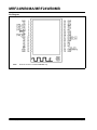
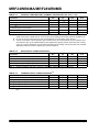
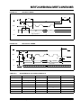
1
MRF24WB0MA/MRF24WB0MB
Data Sheet
2.4 GHz, IEEE Std. 802.11b™
RF Transceiver Module
© 2010 - 2011 Microchip Technology Inc.
DS70632B
Note the following details of the code protection feature on Microchip devices:
•
Microchip products meet the specification contained in their particular Microchip Data Sheet.
•
Microchip believes that its family of products is one of the most secure families of its kind on the market today, when used in the
intended manner and under normal conditions.
•
There are dishonest and possibly illegal methods used to breach the code protection feature. All of these methods, to our
knowledge, require using the Microchip products in a manner outside the operating specifications contained in Microchip’s Data
Sheets. Most likely, the person doing so is engaged in theft of intellectual property.
•
Microchip is willing to work with the customer who is concerned about the integrity of their code.
•
Neither Microchip nor any other semiconductor manufacturer can guarantee the security of their code. Code protection does not
mean that we are guaranteeing the product as “unbreakable.”
Code protection is constantly evolving. We at Microchip are committed to continuously improving the code protection features of our
products. Attempts to break Microchip’s code protection feature may be a violation of the Digital Millennium Copyright Act. If such acts
allow unauthorized access to your software or other copyrighted work, you may have a right to sue for relief under that Act.
Information contained in this publication regarding device
applications and the like is provided only for your convenience
and may be superseded by updates. It is your responsibility to
ensure that your application meets with your specifications.
MICROCHIP MAKES NO REPRESENTATIONS OR
WARRANTIES OF ANY KIND WHETHER EXPRESS OR
IMPLIED, WRITTEN OR ORAL, STATUTORY OR
OTHERWISE, RELATED TO THE INFORMATION,
INCLUDING BUT NOT LIMITED TO ITS CONDITION,
QUALITY, PERFORMANCE, MERCHANTABILITY OR
FITNESS FOR PURPOSE. Microchip disclaims all liability
arising from this information and its use. Use of Microchip
devices in life support and/or safety applications is entirely at
the buyer’s risk, and the buyer agrees to defend, indemnify and
hold harmless Microchip from any and all damages, claims,
suits, or expenses resulting from such use. No licenses are
conveyed, implicitly or otherwise, under any Microchip
intellectual property rights.
Trademarks
The Microchip name and logo, the Microchip logo, dsPIC,
KEELOQ, KEELOQ logo, MPLAB, PIC, PICmicro, PICSTART,
PIC32 logo, rfPIC and UNI/O are registered trademarks of
Microchip Technology Incorporated in the U.S.A. and other
countries.
FilterLab, Hampshire, HI-TECH C, Linear Active Thermistor,
MXDEV, MXLAB, SEEVAL and The Embedded Control
Solutions Company are registered trademarks of Microchip
Technology Incorporated in the U.S.A.
Analog-for-the-Digital Age, Application Maestro, chipKIT,
chipKIT logo, CodeGuard, dsPICDEM, dsPICDEM.net,
dsPICworks, dsSPEAK, ECAN, ECONOMONITOR,
FanSense, HI-TIDE, In-Circuit Serial Programming, ICSP,
Mindi, MiWi, MPASM, MPLAB Certified logo, MPLIB,
MPLINK, mTouch, Omniscient Code Generation, PICC,
PICC-18, PICDEM, PICDEM.net, PICkit, PICtail, REAL ICE,
rfLAB, Select Mode, Total Endurance, TSHARC,
UniWinDriver, WiperLock and ZENA are trademarks of
Microchip Technology Incorporated in the U.S.A. and other
countries.
SQTP is a service mark of Microchip Technology Incorporated
in the U.S.A.
All other trademarks mentioned herein are property of their
respective companies.
© 2010 - 2011, Microchip Technology Incorporated, Printed in
the U.S.A., All Rights Reserved.
Printed on recycled paper.
ISBN: 978-1-61341-261-9
Microchip received ISO/TS-16949:2002 certification for its worldwide
headquarters, design and wafer fabrication facilities in Chandler and
Tempe, Arizona; Gresham, Oregon and design centers in California
and India. The Company’s quality system processes and procedures
are for its PIC® MCUs and dsPIC® DSCs, KEELOQ® code hopping
devices, Serial EEPROMs, microperipherals, nonvolatile memory and
analog products. In addition, Microchip’s quality system for the design
and manufacture of development systems is ISO 9001:2000 certified.
DS70632B-page 2
© 2010 - 2011 Microchip Technology Inc.
MRF24WB0MA/MRF24WB0MB
MRF24WB0MA/MRF24WB0MB Data Sheet
2.4 GHz IEEE Std. 802.11b™
Features:
•
•
•
•
•
•
•
•
•
•
•
•
IEEE Std. 802.11-compliant RF Transceiver
Serialized unique MAC address
Data Rate: 1 and 2 Mbps
IEEE Std. 802.11b/g/n compatible
Small size: 21mm x 31mm 36-pin Surface Mount
Module
Integrated PCB antenna (MRF24WB0MA)
External antenna option (MRF24WB0MB) with
ultra miniature coaxial (U.FL) connector
Range: up to 400m (1300 ft.)
Easy integration into final product – accelerates
product development, provides quicker time to
market
Radio regulation certification for United States
(FCC), Canada (IC), Europe (ETSI) and Japan
(ARIB)
Wi-Fi® certified (WFA ID: WFA7150)
Designed for use with Microchip microcontroller
families (PIC18, PIC24, dsPIC33, and PIC32) with
downloadable Microchip TCP/IP Stack
Operational:
• Single operating voltage: 2.7V–3.6V (3.3V typical)
• Temperature Range: -20° C to +85° C extended
commercial
• Simple, four-wire SPI interface with interrupt
• Low-current consumption:
- RX mode – 85 mA (typical)
- TX mode – 154 mA (+10 dBm typical)
- Sleep – 250 µA (typical)
- Hibernate – <0.1 µA (typical)
RF/Analog Features:
• ISM Band 2.400–2.484 GHz operation
• 14 Channels selectable individually or domainrestricted
• DSSS Modulation
• Data Rate – 1000 kbps
• -91 dBm Typical sensitivity at 1 Mbps
• +10 dBm Typical output power with control
• Integrated low phase noise VCO, RF frequency
synthesizer, PLL loop filter and PA
© 2010–2011 Microchip Technology Inc.
• Digital VCO and filter calibration
• Integrated RSSI ADC and I/Q DACs, RSSI
readings available to host
• Balanced receiver and transmitter characteristics
for low power consumption
MAC/Baseband Features:
• Hardware CSMA/CA access control, automatic
ACK, and FCS creation and checking
• Automatic MAC packet retransmit
• Hardware Security Engine for AES and
RC4-based ciphers
• Supports 802.1x, 802.1i security: WEP,
WPA-PSK, and WPA-2-PSK.
Applications:
• Utility and Smart Energy
- Thermostats
- Smart Meters
- White Goods
- HVAC
• Consumer Electronics
- Remote Control
- Internet Radio
- Home Security
- Toys
• Industrial Controls
- Chemical Sensors
- HVAC
- Security Systems
- M2M Communication
• Remote Device Management
- Location and Asset Tracking
- Automotive
- Code Update
• Retail
- POS Terminals
- Wireless Price Tags
- Digital Remote
• Medical, Fitness, and Health care
- Glucose Meters
- Fitness Equipment
- Patient Asset Tracking
DS70632B-page 3
MRF24WB0MA/MRF24WB0MB
Pin Diagram
Note:
Antenna connector on MRF24WB0MB only.
DS70632B-page 4
© 2010–2011 Microchip Technology Inc.
MRF24WB0MA/MRF24WB0MB
Table of Contents
1.0 Devices Overview......................................................................................................................................................................... 7
2.0 Circuit Description ...................................................................................................................................................................... 13
3.0 Regulatory Approval................................................................................................................................................................... 23
4.0 Electrical Characteristics ............................................................................................................................................................ 27
Appendix A: Revision History............................................................................................................................................................... 31
The Microchip Web Site ....................................................................................................................................................................... 33
Customer Change Notification Service ................................................................................................................................................ 33
Customer Support ................................................................................................................................................................................ 33
Reader Response ................................................................................................................................................................................ 34
Product Identification System .............................................................................................................................................................. 35
TO OUR VALUED CUSTOMERS
It is our intention to provide our valued customers with the best documentation possible to ensure successful use of your Microchip
products. To this end, we will continue to improve our publications to better suit your needs. Our publications will be refined and
enhanced as new volumes and updates are introduced.
If you have any questions or comments regarding this publication, please contact the Marketing Communications Department via
E-mail at [email protected] or fax the Reader Response Form in the back of this data sheet to (480) 792-4150. We
welcome your feedback.
Most Current Data Sheet
To obtain the most up-to-date version of this data sheet, please register at our Worldwide Web site at:
http://www.microchip.com
You can determine the version of a data sheet by examining its literature number found on the bottom outside corner of any page.
The last character of the literature number is the version number, (e.g., DS30000A is version A of document DS30000).
Errata
An errata sheet, describing minor operational differences from the data sheet and recommended workarounds, may exist for current
devices. As device/documentation issues become known to us, we will publish an errata sheet. The errata will specify the revision
of silicon and revision of document to which it applies.
To determine if an errata sheet exists for a particular device, please check with one of the following:
• Microchip’s Worldwide Web site; http://www.microchip.com
• Your local Microchip sales office (see last page)
When contacting a sales office, please specify which device, revision of silicon and data sheet (include literature number) you are
using.
Customer Notification System
Register on our web site at www.microchip.com to receive the most current information on all of our products.
© 2010–2011 Microchip Technology Inc.
DS70632B-page 5
MRF24WB0MA/MRF24WB0MB
NOTES:
DS70632B-page 6
© 2010–2011 Microchip Technology Inc.
MRF24WB0MA/MRF24WB0MB
1.0
DEVICES OVERVIEW
The MRF24WB0MA and MRF24WB0MB are low-power,
2.4 GHz, IEEE Std. 802.11-compliant, surface mount
modules with all associated RF components – crystal
oscillator, bypass and bias passives with integrated
MAC, baseband, RF and power amplifier, and built-in
hardware support for AES, and TKIP (WEP, WPA, WPA2
security). The integrated module design frees the
designer from RF and antenna design tasks and
regulatory compliance testing, ultimately providing
quicker time to market.
The MRF24WB0MA module is approved for use with the
integrated PCB meander antenna.
The MRF24WB0MB comes with an ultra miniature
coaxial connector (U.FL) and is approved for use with
a list of pre-certified antennas. See Section 2.8,
External Antenna, for specific recommendations.
The MRF24WB0MA/MRF24WB0MB modules are
designed to be used with Microchip’s TCP/IP software
stack. The software stack has an integrated driver that
implements the API that is used in the modules for
command and control, and for management and data
packet traffic.
The Microchip TCP/IP software stack is available in the
free Microchip Application Libraries download
(including example applications and source code) from
the Microchip web site, http://www.microchip.com/
wireless.
The combination of the module and a PIC running the
TCP/IP stack results in support for IEEE Standard
802.11 and IP services. This allows, the immediate
implementation of a wireless web server.
© 2010–2011 Microchip Technology Inc.
The MRF24WB0MA/MRF24WB0MB modules have
received regulatory approvals for modular devices in
the United States (FCC), Canada (IC), and Europe
(ETSI). The modular approval removes the need for
expensive RF and antenna design, and allows the end
user to place the modules inside a finished product and
not require regulatory testing for an intentional radiator
(RF transmitter). They also have Radio Type Approval
Certification for Japan. See Section 3.0, Regulatory
Approval, for the specific requirements that should be
adhered to by the integrator.
1.1
Interface Description
The block diagram in Figure 1-1 represents a
MRF24WB0MA/MRF24WB0MB module. It interfaces
to Microchip PIC18, PIC24, dsPIC33, or PIC32
microcontrollers through a four-wire serial slave SPI
interface – interrupt, hibernate, reset, power and
ground signals. The module runs on a single supply
voltage of nominally 3.3V. It also supports optional
JTAG and serial debug for testability. The debug port
operates at 3.3V and requires a level shifter for
operation with RS-232 devices. Figure 1-2 shows a
simplified example connection between a Microchip
PIC MCU and the module. Table 1-1 lists the pin
descriptions.
Data communications with the MRF24WB0MA/
MRF24WB0MB are through the SPI interface that is
detailed in Section 2.0, Circuit Description. The
Microchip PIC microcontroller communicates with the
module through a command API from within the
Microchip TCP/IP stack. The command API is
detailed in the Microchip TCP/IP stack online help
that is included in the free Microchip Application
Libraries download.
DS70632B-page 7
MRF24WB0MA/MRF24WB0MB
FIGURE 1-1:
MRF24WB0MA/MRF24WB0MB BLOCK DIAGRAM
MRF24WB0MA 2. 4 GHz IEEE Std. 802.11b RF Transceiver Module
FLASH
PCB
Antenna
(MRF24WB0MA)
SPI
AES, TKIP
Encryption
Accelerator
Interface
2.4 GHz
Transceiver
RAM
Digital I/O
Interrupt
Power
JTAG
Debug
Matching
Circuitry
Power
Amplifier
ROM
Reset
Hibernate
FIGURE 1-2:
MICROCONTROLLER TO MRF24WB0MA/MRF24WB0MB INTERFACE
MRF24WB0Mx
External
Antenna
(MRF24WB0MB)
PIC Microcontroller
CS
I/O
SDI
SDO
SDO
SDI
SCK
SCK
INT
INTx
+3.3V (Typ)
VDD
HIBERNATE
I/O
GND
GND
WP
I/O
RESET
I/O
DS70632B-page 8
© 2010–2011 Microchip Technology Inc.
MRF24WB0MA/MRF24WB0MB
TABLE 1-1:
Pin Description
Pin
Symbol
Type
1
GND
P
2
NC
NC
3
JTAGTDO
O
Description
Ground
Do not connect
JTAG test data output
(1)
4
JTAGTCK
5
JTAGTMS
6
JTAGTDI
I
JTAG test data input
7
RESET
I: Constant(1)
Module Reset input
8
NC
NC
I: Constant
I
JTAG clock input
JTAG mode input
Do not connect
9
JTAGRST
I
JTAG Reset input (optional; see Section 2.0, Circuit Description)
10
GND
P
Ground
11
NC
NC
Do not connect
12
NC
NC
Do not connect
13
NC
NC
Do not connect
14
NC
NC
Do not connect
15
NC
NC
Do not connect
16
WP(2)
I
Write protect (this pin is used to enable FLASH update)
17
VDD
P
Power
18
GND
P
Ground
19
GND
P
Ground
20
HIBERNATE
I
Hibernate mode enable (high input will disable the module)
21
JTAGEN
I
JTAG test enable
22
NC
NC
23
CS
I: Constant(1)
24
NC
NC
25
GND
P
Ground
26
DEBUGRX
I
Serial debug port input (see Section 2.0, Circuit Description)
27
DEBUGTX
O
Serial debug port output (see Section 2.0, Circuit Description)
28
GND
P
Ground
29
VDD
P
Power
30
GND
P
Ground
31
NC
NC
32
SDO
O
SPI data out
Do not connect
SPI Chip Select input, constant drive or pull-up required
Do not connect
Do not connect
33
INT
O
Interrupt output (open drain – requires a pull-up)
34
SCK
I
SPI clock input
35
SDI
I
SPI data in
36
GND
P
Ground
Legend: Pin type abbreviation: P = Power input, I = Input, O = Output, NC = Do Not Connect
Note 1:
2:
Signals of Type “I: Constant” must either be constantly driven by the host or have a pull-up or pull-down (in
case the host is likely to tri-state the signal during power down modes). The constant drive is used to
ensure defined operation of the part and to minimize leakage current during low power modes.
WP is used as write-protect for the internal module SPI Flash. For production use, this pin should be
pulled low. This pin can be controlled by the host microcontroller to enable in field Flash updates.
© 2010–2011 Microchip Technology Inc.
DS70632B-page 9
MRF24WB0MA/MRF24WB0MB
1.2
Mounting Details
The MRF24WB0MA/MRF24WB0MB is a surface
mountable module. Module dimensions are shown in
Figure 1-3. The module Printed Circuit Board (PCB) is
1 mm thick with castellated mounting points on two
sides.
FIGURE 1-3:
MRF24WB0MA/MRF24WB0MB MODULE PHYSICAL DIMENSIONS
Note:
DS70632B-page 10
Antenna connector on
MRF24WB0MB only.
© 2010–2011 Microchip Technology Inc.
MRF24WB0MA/MRF24WB0MB
Figure 1-4 shows the recommended host PCB footprint
for the module.
The MRF24WB0MA has an integrated PCB antenna.
For best performance, follow the mounting details
shown in Figure 1-4.
FIGURE 1-4:
For best performance, mount the module on the PCB
without metal obstructions in the keep out area of
Figure 1-4. The antenna is tuned to have FR4 PCB
material underneath the module. Do not “cut-out” host
PCB material under the antenna.
RECOMMENDED HOST PCB FOOTPRINT
Note 1: The “Note 1” demarcation specifies the host PCB copper plane keep-out area on underlying
board layers. It is alright to route surface escape traces in this area.
© 2010–2011 Microchip Technology Inc.
DS70632B-page 11
MRF24WB0MA/MRF24WB0MB
Figure 1-5 illustrates the module reflow profile that is
recommended for mounting the device onto the host
PCB.
FIGURE 1-5:
RECOMMENDED MODULE REFLOW PROFILE AND SETPOINTS
2
1
3
4
5
Zones
6
7
8
300
Temperature (°C)
250
200
150
100
50
0
0
50
100
150
200
250
300
Time (Seconds)
TABLE 1-2:
MODULE REFLOW PROFILE(1)
Zone
Temperature (°C)
Note 1:
1
2
3
4
5
6
7
8
180°
180°
200°
200°
200°
220°
265°
270°
Conveyor Speed: 90 cm/min
DS70632B-page 12
© 2010–2011 Microchip Technology Inc.
MRF24WB0MA/MRF24WB0MB
2.0
CIRCUIT DESCRIPTION
The MRF24WB0MA/MRF24WB0MB interfaces to
Microchip PIC18, PIC24, dsPIC33, and PIC32
microprocessors with a minimal of external
components through digital-only connections. This
section details use of the module, starting with an
example host connection as shown in Figure 2-1.
2.1
Schematic
FIGURE 2-1:
2.2
MRF24WB0MA/MRF24WB0MB EXAMPLE APPLICATION SCHEMATIC
Power-On Sequence
The internal regulators for the digital and analog core
power supplies are disabled by driving the
HIBERNATE pin high. Figure 2-2 shows the power up
sequence for the MRF24WB0MA/MRF24WB0MB.
There is an internal Power-on-Reset (POR) circuit
which keeps the module in reset until VDD is within
specification. The Hibernate and Reset signals are also
used to control startup. In Figure 2-2, section A is
controlled by the internal POR and section B is an
allowance for the SPI bus to stabilize when the module
supplies are enabled. Once Hibernate is disabled, the
host software provides 1mS of startup to allow the SPI
to stabilize. This time is pre-programmed into the host
driver, and may need to be increased if insufficient
initial drive current is not provided to the MRF24WB0M
module. Section C is the driver controlled release from
Reset period. This takes approximately 300 mS and is
monitored by the stack driver. No additional time needs
to be provided by user software for startup.
© 2010–2011 Microchip Technology Inc.
DS70632B-page 13
MRF24WB0MA/MRF24WB0MB
FIGURE 2-2:
DS70632B-page 14
MRF24WB0MA/MRF24WB0MB POWER-ON SEQUENCE TIMING
© 2010–2011 Microchip Technology Inc.
MRF24WB0MA/MRF24WB0MB
2.3
Power States
2.3.2
The MRF24WB0MA/MRF24WB0MB has several
power states. These are Hibernate, Sleep and Active
(two sub-states), as shown in Figure 2-3. The selection
of power state directly affects system behavior, and
overall power consumption or battery life. There is also
a “Standby” state that is not user-controlled.
2.3.1
HIBERNATE STATE
An “Off” state is defined as no power applied to the
device. The Hibernate mode is the closest to controlled
off that the module can approach. It is controlled
through the HIBERNATE pin (high input puts the
module into Hibernate). When in Hibernate, the module
only consumes leakage current, but does not maintain
state. Hibernate has to be fully controlled by the PIC
MCU and requires the TCP/IP stack to restart on an
awake.
The module contains about 70µF of internal bulk
capacitance. Supplies should be provisioned to supply
sufficient charge on release of hibernate for desired
start time or sufficient delay must be provided in
software after hibernate release and before releasing
reset.
This state provides the best battery life for embedded
products. Entering Hibernate for intervals of less than
30 seconds is not likely to save power. Battery life
expectation can be more than a year for devices
operating on AA cells that would be in Hibernate except
to wake up every hour for a small data transfer (<500
Bytes).
TABLE 2-1:
State
SLEEP STATE
The Sleep state is a low power dynamic state that
automatically implements the 802.11 Power Save
feature. In this mode, if enabled, the module will enter
Power Save mode when all activity is complete.
The module will wake autonomously to any PIC
intervention so it can check DTIM beacons from the
Access Point. If any traffic is listed as queued for the
module, then it will awaken and get the data from the
Access Point on the next possible opportunity. When
data is acquired, the module will interrupt the PIC
microcontroller on a normal “data available” indication.
If no data is available on a DTIM check, the module
reenters the Power Save state until the next DTIM. The
DTIM interval is programmed at the Access Point. This
state can provide “as if on” behavior of the radio with a
significant power savings versus “always on”. The
battery life expectation of this mode is several days to
several weeks. This mode is characterized by a very
low latency (as low as 200 mS) to begin data transfer
from the low power state.
2.3.3
ACTIVE STATE
The Active state is identified as one of two states where
the radio circuitry is fully on. The two active states are
the Receive state (RX ON) and the Transmit state (TX
ON).
2.3.4
STANDBY STATE
The Standby state is not user-controlled but is noted as
it helps identify and track certain operations of the
module during power tracing.
MRF24WB0MA/MRF24WB0MB POWER STATE DEFINITIONS
VDD
CS
Description
Power is completely disconnected
Off
0V
0V
Hibernate
3.3V
3.3V
All internal power regulators are OFF – enabled by HIBERNATE pin
Sleep
3.3V
0V
Enabled by TCP/IP driver
RX ON
3.3V
0V
Receive circuits are on and receiving
TX ON
3.3V
0V
Transmit circuits are on and transmitting
Standby
3.3V
0V
State machine transition state only – not user controlled
© 2010–2011 Microchip Technology Inc.
DS70632B-page 15
MRF24WB0MA/MRF24WB0MB
FIGURE 2-3:
MRF24WB0MA/MRF24WB0MB POWER-STATE DIAGRAM
10 µs
Off
RX On
TX On
Note 1
200 µs
Hibernate
Standby
Note 1
200 µs
Sleep
Note 1: See Section 2.2, Power-On Sequence.
2.4
JTAG Interface
Joint Test Action Group (JTAG) is the common name
used for the IEEE 1149.1 standard entitled Standard
Test Access Port and Boundary-Scan Architecture for
test access ports that are used for testing printed circuit
boards using boundary scan. The MRF24WB0MA/
MRF24WB0MB supports JTAG boundary scan. The
JTAG port provides the optional hardware JTAG Reset
input, JTAGRST. JTAG_EN and JTAGRST need to be
driven high to enable JTAG mode. JTAG should not be
enabled during normal functional operation. This
function affects power state current.
DS70632B-page 16
2.5
Debug Serial Interface
The MRF24WB0MA/MRF24WB0MB incorporates a
Transmit Data pin (DEBUGTX) and a Receive Data pin
(DEBUGRX) for serial debugging purposes. These pins
can be connected to commercially available RS-232 line
drivers/receivers with appropriate external level shifters.
The serial interface operates at 19200, 8, N, 1, N.
© 2010–2011 Microchip Technology Inc.
MRF24WB0MA/MRF24WB0MB
2.6
SPI Interface
2.7
PCB Antenna
The slave Serial Peripheral Interface (SPI) is used to
interface with the host PIC microcontroller. The slave
SPI interface works with the Interrupt line (INT). When
data is available for the PIC microcontroller during
operation, the INT line is asserted (logic low) by the
MRF24WB0MA/MRF24WB0MB module. The INT line
is de-asserted (logic high) by the MRF24WB0MA/
MRF24WB0MB after the data is transferred to the host
PIC microcontroller. The SPI SCK frequency can be up
to 25 MHz.
For the MRF24WB0MA, the PCB antenna is fabricated
on the top copper layer and covered in solder mask.
The layers below the antenna have no copper trace.
The slave SPI interface implements the [CPOL=0;
CPHA=0] and [CPOL=1; CPHA=1] modes (0 and 3) of
operation. That is, data is clocked in on the first rising
edge of the clock after Chip Select (CS) is asserted.
The antenna patterns shown in the following plots, designated as Figure 2-4, Figure 2-5 and Figure 2-6, refer
to three separate axis of measurement that correspond
to the orientation of the module (drawn in the center of
each plot).
Data is placed on the bus with most significant bit
(MSb) first.
The CS pin must be toggled with transfer blocks and
cannot be held low permanently. The falling edge of CS
is used to indicate the start of a transfer. The rising
edge of CS is used to indicate the completion of a
transfer.
Figure 4-1 in Section 4.0, Electrical Characteristics
shows the SPI timing diagram. Table 4-7 details the
SPI timing AC characteristics.
© 2010–2011 Microchip Technology Inc.
It is recommended that the module be mounted on the
edge of the host PCB. It is permitted for PCB material
to be below the antenna structure of the module as long
as no copper traces or planes are on the host PCB in
that area. For best performance, place the module on
the host PCB according to the details shown in
Figure 1-4.
The horizontal and vertical data, blue and red
respectively, in each plot correspond to the orientation
(polarization) of the measurement antenna rotated 360
degrees around the module.
The horizontal measurement was done with the receive
antenna parallel with the module PCB. The vertical
measurement was done perpendicular to the module
PCB.
These patterns allow the designer to understand the
performance of the module with respect to the position
of the receive/transmit antenna at the other end of the
link. Figure 2-4, Figure 2-5 and Figure 2-6 show the
simulated radiation patterns expected from the PCB
antenna.
DS70632B-page 17
MRF24WB0MA/MRF24WB0MB
FIGURE 2-4:
AZIMUTH RADIATION PATTERN, 2.44GHZ
0°
0 dB
-5 dB
Horizontal
-10 dB
-15 dB
Vertical
-20 dB
270°
90°
180°
DS70632B-page 18
© 2010–2011 Microchip Technology Inc.
MRF24WB0MA/MRF24WB0MB
FIGURE 2-5:
RADIATION PATTERN ON SIDE WITH PCB ANTENNA, 2.44GHZ
0°
0 dB
-5 dB
Horizontal
-10 dB
-15 dB
Vertical
-20 dB
270°
90°
180°
© 2010–2011 Microchip Technology Inc.
DS70632B-page 19
MRF24WB0MA/MRF24WB0MB
FIGURE 2-6:
RADIATION PATTERN ALONG PIN EDGE, 2.44GHZ
0°
0 dB
-5 dB
Horizontal
-10 dB
-15 dB
-20 dB
270°
90°
Vertical
180°
DS70632B-page 20
© 2010–2011 Microchip Technology Inc.
MRF24WB0MA/MRF24WB0MB
2.8
External Antenna
The MRF24WB0MB has been regulatory certified for
use with a number of antennas. The modular
certifications hold only if the following antennas, or
antennas that are materially and functionally
equivalent, are used. All antennas connect to the
module through an ultra miniature coaxial (U.FL or
IPEX) connector.
A list of antennas for use with the module is provided in
Table 2-2.
TABLE 2-2:
LIST OF CERTIFIED EXTERNAL ANTENNAS
Part Number
RFA-02-P05
Type
Gain (dBi)
VSWR
Max.
Connector
Vendor
PCB
2
2.0
IPEX
Aristotle
RFA-02-L6H1-70-35
Dipole
2
2.0
IPEX
Aristotle
RFA-02-D3
Dipole
1.5
2.0
IPEX
Aristotle
RFA-02-L2H1
Dipole
2
2.0
IPEX
Aristotle
RFA-02-3-C5H1
Dipole
3
2.0
IPEX
Aristotle
RFA-02-5-C7H1
Dipole
5
2.0
IPEX
Aristotle
RFA-02-5-F7H1
Dipole
5
2.0
IPEX
Aristotle
WF2400-15001A
Dipole
5
2.0
IPEX
Saytec
WF2400-15001AR
Dipole
5
2.0
RF-IPEX
Saytec
WF2400-10001I
Dipole
2
2.0
IPEX
Saytec
WF2400-10001R
Dipole
2
2.0
RF-IPEX
Saytec
AN2400-5901RS, used with connector
SMASFR8-3152H-00X00I
Omni
9
2.0
IPEX
Saytec
AN2400-5901RS, used with connector
SMASFR8-3152H-00X00IR
Omni
9
2.0
RF-IPEX
Saytec
© 2010–2011 Microchip Technology Inc.
DS70632B-page 21
MRF24WB0MA/MRF24WB0MB
NOTES:
DS70632B-page 22
© 2010–2011 Microchip Technology Inc.
MRF24WB0MA/MRF24WB0MB
3.0
REGULATORY APPROVAL
The MRF24WB0MA/MRF24WB0MB module has
received regulatory approvals for modular devices in
the United States, Canada and European countries.
Modular approval allows the end user to place the
MRF24WB0MA/MRF24WB0MB module inside a
finished product and not require regulatory testing for
an intentional radiator (RF transmitter), provided no
changes or modifications are made to the module
circuitry. Changes or modifications could void the
user’s authority to operate the equipment. The end
user must comply with all of the instructions provided
by the Grantee, which indicate installation and/or
operating conditions necessary for compliance.
The integrator may still be responsible for testing the
end product for any additional compliance
requirements that become necessary with this module
installed (for example, digital device emission, PC
peripheral requirements, etc.) in the specific country
that the end device will be marketed.
Refer to the specific country radio regulations for
details on regulatory compliance.
3.1
United States
The MRF24WB0MA/MRF24WB0MB has received
Federal Communications Commission (FCC) CFR47
Telecommunications, Part 15 Subpart C “Intentional
Radiators” 15.247 and modular approval in accordance
with FCC Public Notice DA 00-1407 Released: June
26, 2000, Part 15 Unlicensed Modular Transmitter
Approval. The MRF24WB0MA/MRF24WB0MB module
can be integrated into a finished product without
obtaining subsequent and separate FCC approvals for
intentional radiation.
A user’s manual for the product should include the
following statement:
This equipment has been tested and found to
comply with the limits for a Class B digital device,
pursuant to part 15 of the FCC Rules. These limits
are designed to provide reasonable protection
against harmful interference in a residential
installation. This equipment generates, uses and
can radiate radio frequency energy, and if not
installed and used in accordance with the
instructions, may cause harmful interference to
radio communications. However, there is no
guarantee that interference will not occur in a
particular installation. If this equipment does cause
harmful interference to radio or television
reception, which can be determined by turning the
equipment off and on, the user is encouraged to try
to correct the interference by one or more of the
following measures:
• Reorient or relocate the receiving antenna.
• Increase the separation between the equipment
and receiver.
• Connect the equipment into an outlet on a circuit
different from that to which the receiver is
connected.
• Consult the dealer or an experienced radio/TV
technician for help.
The MRF24WB0MA/MRF24WB0MB module has been
labeled with its own FCC ID number, and if the FCC ID
is not visible when the module is installed inside
another device, then the outside of the finished product
into which the module is installed must also display a
label referring to the enclosed module. The following
examples present terminology that could be used:
Contains Transmitter Module FCC ID:
W7OZG2100-ZG2101
or
Contains FCC ID: W7OZG2100-ZG2101
This device complies with Part 15 of the FCC
Rules. Operation is subject to the following two
conditions:
(1) this device may not cause harmful interference,
and (2) this device must accept any interference
received, including interference that may cause
undesired operation.
© 2010–2011 Microchip Technology Inc.
DS70632B-page 23
MRF24WB0MA/MRF24WB0MB
3.1.1
RF EXPOSURE
3.2
Canada
All transmitters regulated by FCC must comply with RF
exposure requirements. OET Bulletin 65, Evaluating
Compliance with FCC Guidelines for Human Exposure
to Radio Frequency Electromagnetic Fields, provides
assistance in determining whether proposed or existing
transmitting facilities, operations or devices comply
with limits for human exposure to Radio Frequency
(RF) fields adopted by the Federal Communications
Commission (FCC). The bulletin offers guidelines and
suggestions for evaluating compliance.
The MRF24WB0MA/MRF24WB0MB module has been
certified for use in Canada under Industry Canada (IC)
Radio Standards Specification (RSS) “RSS-210” and
“RSS-Gen”.
If appropriate, compliance with exposure guidelines for
mobile and unlicensed devices can be accomplished
by the use of warning labels and by providing users
with information concerning minimum separation
distances from transmitting structures and proper
installation of antennas.
a)The host device, as a stand-alone unit without
any separately certified modules, complies
with all applicable Radio Standards
Specifications.
b)The host device and all the separately certified
modules it contains jointly meet the RF exposure compliance requirements of “RSS-102”, if
applicable.
c)The host device complies with the certification
labeling requirements of each of the modules
it contains.”
The following statement must be included as a
CAUTION statement in manuals and OEM products to
alert users of FCC RF exposure compliance:
To satisfy FCC RF Exposure requirements for
mobile and base station transmission devices, a
separation distance of 20 cm or more should be
maintained between the antenna of this device and
persons during operation. To ensure compliance,
operation at closer than this distance is not
recommended.
The antenna(s) used for this transmitter must not
be co-located or operating in conjunction with any
other antenna or transmitter.
If the MRF24WB0MA/MRF24WB0MB module is used
in a portable application (i.e., the antenna is less than
20 cm from persons during operation), the integrator is
responsible for performing Specific Absorption Rate
(SAR) testing in accordance with FCC rules 2.1091.
3.1.2
HELPFUL WEB SITES
Federal Communications Commission (FCC):
http://www.fcc.gov.
From “Section 7.1.1, RSS-Gen”, Issue 2, June 2007,
Modular Transmitter Approval:
“Host devices which contain separately certified
modules do not need to be recertified, provided
that they meet the following conditions:
The following
compliance.
example
demonstrates
labeling
NOTE: Compliance of a module in its final
configuration is the responsibility of the applicant.
A host device will not be considered certified if the
instructions regarding antenna configuration
provided in the original description, of one or more
separately certified modules it contains, were not
followed.
From “Section 5.2, RSS-Gen”, Issue 2, June 2007,
Equipment Labels:
“All Category I radio equipment intended for use
in Canada shall permanently display on each
transmitter, receiver or inseparable combination
thereof, the applicant’s name (i.e., manufacturer’s
name, trade name or brand name), model
number and certification number. This information
shall be affixed in such a manner as to not be
removable except by destruction or defacement.
The size of the lettering shall be legible without
the aid of magnification, but is not required to be
larger than 8-point font size. If the device is too
small to meet this condition, the information can
be included in the user manual upon agreement
with Industry Canada.”
The label is shown in the following example:
Contains IC: 8248A-G21ZEROG
DS70632B-page 24
© 2010–2011 Microchip Technology Inc.
MRF24WB0MA/MRF24WB0MB
From “Section 7.1.6, RSS-Gen”, Issue 2, June 2007,
Digital Circuits:
“If the device contains digital circuitry that is not
directly associated with the radio transmitter, the
device shall also have to comply with ICES-003,
Class A or B as appropriate, except for ICES-003
labeling requirements. The test data obtained (for
the ICES-003 tests) shall be kept by the
manufacturer or importer whose name appears
on the equipment label, and made available to
Industry Canada on request, for as long as the
model is being marketed in Canada.”
3.2.1
HELPFUL WEB SITES:
Industry Canada: http://www.ic.gc.ca/
3.3
Europe
The MRF24WB0MA/MRF24WB0MB module has been
certified for use in European countries. The following
testing has been completed:
Test standard ETSI EN 300 328 V1.7.1 (2006-10):
•
•
•
•
Maximum Transmit Power
Maximum EIRP Spectral Density
Frequency Range
Radiated Emissions
Test standards ETSI EN 301 489-1:2008 and ETSI EN
301 489-17:2008:
• Radiated Emissions
• Electro-Static Discharge
• Radiated RF Susceptibility
The modules are fully compliant with
•
•
•
•
•
•
Radiated Emissions EN 55022
Electrostatic Discharge EN 61000-4-2
Radiated Immunity EN 61000-4-3
EN 60950-1
CE-Mark
RoHS
The end user is responsible for ensuring compliance
with
harmonized
frequencies
and
labeling
requirements for each country in which the end device
is marketed and sold.
3.3.1
HELPFUL WEB SITES:
Radio and Telecommunications Terminal Equipment
(R&TTE):
http://ec.europa.eu/enterprise/rtte/index_en.htm
European
Conference
of
Postal
Telecommunications Administrations (CEPT):
and
http://www.cept.org/
European Telecommunications Standards Institute
(ETSI):
http://www.etsi.org/
European Radio Communications Office (ERO):
http://www.ero.dk/
3.4
Should other regulatory jurisdiction certification be
required by the customer, or the customer need to
recertify the module for other reasons, a certification
utility is available. The utility runs on a Window's PC
and utilizes a USB to SPI converter to interface to the
MRF24WB0M module. In order to use the utility, the
MRF24WB0M module must be out of reset and not
accessed by the system host. That is, the SPI signals
to the MRF24WB0M must be tri-state, with Reset and
Hibernate deasserted. The following signals will need
to be brought from the MRF24WB0M for connection to
the PC (through the USB adapter):
•
•
•
•
•
•
SDO
SDI
CS
SCK
INT
GND
For further regulatory Certification Utility and
documentation, contact your local Microchip
salesperson.
ETSI does not provide a modular approval similar to
the USA (FCC) and Canada (IC). However, the testing
completed above can be used as part of the customer’s
application for certification. The test report data can be
included in their test plan and can significantly the
lower customer’s certification burden.
A helpful document that can be used as a starting point
in understanding the use of Short Range Devices
(SRD) in Europe is the European Radio
Communications Committee (ERC) Recommendation
“70-03 E”, downloadable from the European Radio
Communications Office (ERO): http://www.ero.dk/
© 2010–2011 Microchip Technology Inc.
DS70632B-page 25
MRF24WB0MA/MRF24WB0MB
3.5
Wi-Fi® Alliance
Wi-Fi Alliance Certification focuses on interoperability
testing of devices based on 802.11 standards.
Historically, when the certification process and
programs were developed by Wi-Fi Alliance members,
the vast majority of the 802.11 clients were PC-centric,
and certification testing adequately addressed those
types of devices. In subsequent years, the number of
Wi-Fi devices that are not PC-centric has grown
significantly.
These non-standard devices, as a class of products,
have been dubbed Application Specific Devices
(ASDs) by the Wi-Fi Alliance. ASDs are 802.11
devices, for example clients or access points (APs),
which cannot be tested under a standard Alliance test
plan because they do not comply with the standard test
configuration and/or because they are designed to
perform a specific application. Examples include, but
are not limited to: bar code scanners, pagers, recording
devices, monitoring equipment, and cable modems.
The APs or clients that are used to validate ASD
compliance (from the standard test bed) will meet all of
the requirements specified in the applicable System
Interoperability Test Plans (referred to as the “standard
test plan”), unless specifically exempted. The
MRF24WB0MA and MRF24WB0MB modules are in
the ASD category.
The modules are certified under Wi-Fi 802.11 with
WPA2, WPA, and WEP System Interoperability ASD
Model Test Plan with Test Engine For IEEE 802.11a, b,
and g Devices (Version 1.0).
DS70632B-page 26
Per the Wi-Fi Alliance approved ASD test plan, the
definition of the Microchip MRF24WB0MA and
MRF24WB0MB modular solutions is expressed in the
following statements:
“Member Wireless solution is a single-chip
802.11b module including MAC, baseband, RF
and power amplifier personal STA. It utilizes a
simple to use API for embedded markets, and an
OS is not a requirement for operation. It supports
1 and 2 Mbps (TX and RX). It also supports WEP,
WPA Personal, and WPA2 Personal security.
Ciphers supported are AES and TKIP. The
Member Wireless solution interfaces with the
HOST through SPI Bus. Some applications for
the Member Wireless solution are as following:
• Sensors/Controls such as Industrial & Factory
sensors, HVAC, & Lighting
• Consumer Electronic such as remote controls,
toys, and internet radio
This certification ensures that the MRF24WB0MA
and MRF24WB0MB modules have passed
rigorous testing for interoperability across existing
consumer and business Wi-Fi equipments, and
their certifications are completed (WFA ID:
WFA7150). The certification effort undertaken will
save customers time and money. For modular
policy, refer to WFA Module Policy (Version 2.2;
MARCH 2006).”
© 2010–2011 Microchip Technology Inc.
MRF24WB0MA/MRF24WB0MB
4.0
ELECTRICAL
CHARACTERISTICS
TABLE 4-1:
DIGITAL ELECTRICAL CHARACTERISTICS (NOMINAL CONDITIONS: 25C,
VDD = 3.3V)
Parameters
Min
Typ
Max
Units
VIL (Input low voltage)
-0.3
—
0.8
V
VIH (Input high voltage)
2
—
5.5
V
VOL (Output low voltage)
—
—
0.4
V
VOH (Output high voltage)
2.4
—
—
V
IOL (Output low level current at VOL Max)
—
8.5
—
mA
IOH (Output high level current at VOH Min)
—
15.4
—
mA
TABLE 4-2:
ABSOLUTE MAXIMUM RATINGS(1)
Parameters
Min
Max
Storage Temperature
-40C
+125C
VDD
0V
Notes
—
4.2V for 0.5mSec VDD above this level and duration will disable Radio
VIN on SDI, CS, SCK
-0.3V
5.5V
—
Note 1: Listed Absolute Maximum Ratings are not meant for functional operation. Operation at these levels is not
guaranteed, and may reduce the operating life of the component.
TABLE 4-3:
RECOMMENDED OPERATING CONDITIONS
Parameters
Ambient
Temperature(2)
Min
Typ
Max
Units
-20
—
+85
Degrees Celsius
3.63(1)
VDD – for FCC and IC
2.70
3.3
Volts
Note 1: While 3.63V is the maximum operating voltage, the module will detect an overvoltage condition at 4.2V and
disable the RF Transmit function after 0.5 ms. This is an RF certification requirement pertaining to disabling
transmission in unforeseen overvoltage conditions.
2: Ambient temperature for industrial part number is minimum -40C to maximum +85C. Contact Microchip
Sales for industrial temperature parts.
© 2010–2011 Microchip Technology Inc.
DS70632B-page 27
MRF24WB0MA/MRF24WB0MB
TABLE 4-4:
CURRENT CONSUMPTION(3) (NOMINAL CONDITIONS: 25C, VDD = 3.3V)
Parameters
IDD, Hibernate = 3.3V
Min
Typ
Max
Units
—
0.1
—
µA
(1)
IDD, Sleep (software enabled)
—
250
—
µA
IDD, Standby (transitional state)
—
10
—
mA
IDD core(2), RX on, Receive @-83dBm with 2Mbps
modulated signal at antenna port
—
85
—
mA
IDD core, TX on, +0 dBm
—
115
—
mA
IDD core, TX on, +10 dBm
—
154
—
mA
Note 1: Sleep current is current consumed during periods of “standby” between DTIM beacons. The module will
awake 2 mS before a DTIM and turn on its receiver, and possibly its transmitter (if data is available for it).
2: IDD core is current consumed by the part not including the I/O consumption of the SPI port.
3: Current Consumption values represent Typical Peak currents, and the measured current conditions were
done with 85% duty cycle modulated signal. Wi-Fi applications typically operate at less than 85% TX duty
cycle. TX current is dependent on such criteria as transmit power setting, and transmit data rate and bandwidth being used. RX current is affected by connection distance.
TABLE 4-5:
RECEIVER AC CHARACTERISTICS(1)
Parameters
Min
Typ
Max
Units
Flo
2412
—
2484
MHz
RX Min Input Level Sensitivity, 1Mbps, 8% PER
—
-91
—
dBm
RX Min Input Level Sensitivity, 2Mbps, 8% PER
—
-88
—
dBm
RX Max Input Level (Power), 1Mbps, 8% PER
—
-4
—
dBm
RX Max Input Level (Power), 2Mbps, 8% PER
—
-4
—
Note 1: Nominal conditions: 25C, VDD = 3.3V, Flo = 2437 MHz, measurements at antenna port.
dBm
TABLE 4-6:
TRANSMITTER AC CHARACTERISTICS(1)
Parameters
Min
Typ
Max
Units
Flo
2412
—
2484
MHz
Average Pout (transmit spectrum mask compliant)
—
+10
—
dBm
Average Pout gain step resolution from +5 to +10dBm
—
0.5
—
dB
Average Pout gain step resolution from -5 to +5dbm
—
1.0
—
dB
Average Pout settled variation
-0.5
—
0.5
dB
Note 1: Nominal conditions: 25C, VDD = 3.3V, Flo = 2437 MHz, 2 Mbps. modulated signal measured at antenna
port.
DS70632B-page 28
© 2010–2011 Microchip Technology Inc.
MRF24WB0MA/MRF24WB0MB
FIGURE 4-1:
SPI INPUT TIMING
TCSD
TSCK
CS
TCSH
TCSS
SCK
TSU
SI
THD
MSb In
LSb In
High-Impedance
SO
CS must be toggled for each SPI block transfer.
FIGURE 4-2:
SPI OUTPUT TIMING
CS
TSCK
SCK
TV
SO
TV
TDIS
MSb Out
LSb Out
Don’t Care
SI
LSb In
TABLE 4-7:
SPI INTERFACE AC CHARACTERISTICS
Symbol
Parameters
Min
Max
Units
TSCK
SCK Period
40
—
nS
TCSD
CS High time
50
—
nS
TCSS
CS Setup time
50
—
nS
TCSH
CS Hold time
50
—
nS
TSU
SDI Setup time
10
—
nS
THD
SDI Hold time
10
—
nS
TV
SDO Valid time
—
15
nS
© 2010–2011 Microchip Technology Inc.
DS70632B-page 29
MRF24WB0MA/MRF24WB0MB
NOTES:
DS70632B-page 30
© 2010–2011 Microchip Technology Inc.
MRF24WB0MA/MRF24WB0MB
APPENDIX A:
REVISION HISTORY
Revision A (April 2010)
This is the initial release of the document.
Revision B (June 2011)
This revision includes the following updates:
• Updated Section , Operational: Changed
temperature range to -20° C to +85° C
• Updated Table 1-1: Added type and pin
description to pin 23.
• Updated Table 4-3
• Replaced Figure 2-2
• Updated Section 2.0, Circuit Description
• Added Section 3.4,
• Updated the temperature on the order code in
Section , Product Identification System
• Minor changes to the text and formatting were
incorporated throughout the document.
© 2010–2011 Microchip Technology Inc.
DS70632B-page 31
MRF24WB0MA/MRF24WB0MB
NOTES:
DS70632B-page 32
© 2010–2011 Microchip Technology Inc.
MRF24WB0MA/MRF24WB0MB
THE MICROCHIP WEB SITE
CUSTOMER SUPPORT
Microchip provides online support via our WWW site at
www.microchip.com. This web site is used as a means
to make files and information easily available to
customers. Accessible by using your favorite Internet
browser, the web site contains the following
information:
Users of Microchip products can receive assistance
through several channels:
• Product Support – Data sheets and errata,
application notes and sample programs, design
resources, user’s guides and hardware support
documents, latest software releases and archived
software
• General Technical Support – Frequently Asked
Questions (FAQ), technical support requests,
online discussion groups, Microchip consultant
program member listing
• Business of Microchip – Product selector and
ordering guides, latest Microchip press releases,
listing of seminars and events, listings of
Microchip sales offices, distributors and factory
representatives
•
•
•
•
•
Distributor or Representative
Local Sales Office
Field Application Engineer (FAE)
Technical Support
Development Systems Information Line
Customers
should
contact
their
distributor,
representative or field application engineer (FAE) for
support. Local sales offices are also available to help
customers. A listing of sales offices and locations is
included in the back of this document.
Technical support is available through the web site
at: http://microchip.com/support
CUSTOMER CHANGE NOTIFICATION
SERVICE
Microchip’s customer notification service helps keep
customers current on Microchip products. Subscribers
will receive e-mail notification whenever there are
changes, updates, revisions or errata related to a
specified product family or development tool of interest.
To register, access the Microchip web site at
www.microchip.com. Under “Support”, click on
“Customer Change Notification” and follow the
registration instructions.
© 2010–2011 Microchip Technology Inc.
DS39957C-page 33
MRF24WB0MA/MRF24WB0MB
READER RESPONSE
It is our intention to provide you with the best documentation possible to ensure successful use of your Microchip
product. If you wish to provide your comments on organization, clarity, subject matter, and ways in which our
documentation can better serve you, please FAX your comments to the Technical Publications Manager at
(480) 792-4150.
Please list the following information, and use this outline to provide us with your comments about this document.
TO:
Technical Publications Manager
RE:
Reader Response
Total Pages Sent ________
From: Name
Company
Address
City / State / ZIP / Country
Telephone: (_______) _________ - _________
FAX: (______) _________ - _________
Application (optional):
Would you like a reply?
Y
N
Device: MRF24WB0MA/MRF24WB0MB
Literature Number: DS39957C
Questions:
1. What are the best features of this document?
2. How does this document meet your hardware and software development needs?
3. Do you find the organization of this document easy to follow? If not, why?
4. What additions to the document do you think would enhance the structure and subject?
5. What deletions from the document could be made without affecting the overall usefulness?
6. Is there any incorrect or misleading information (what and where)?
7. How would you improve this document?
DS39957C-page 34
© 2010–2011 Microchip Technology Inc.
MRF24WB0MA/MRF24WB0MB
PRODUCT IDENTIFICATION SYSTEM
To order parts, including industrial, or obtain information, for e.g., on pricing or delivery, refer to the factory or the listed sales office.
PART NO.
M
X
T
-X
Device
Module
Module
Type
Tape and
Reel
Temperature
Range
Examples:
a)
b)
Device
Temperature Range
MRF24WB0MA/RM = Extended commercial
temp. tray
MRF24WB0MB/RM = Extended commercial
temp. tray
MR24WB0MA/MRF24WB0MB;
VDD range 2.7V to 3.6V
-20°C to
+85°C
(Extended commercial)
-40°C to
+85°C
(Industrial Temp)
© 2010–2011 Microchip Technology Inc.
DS70632B-page
MRF24WB0MA/MRF24WB0MB
NOTES:
DS70632B-page
© 2010–2011 Microchip Technology Inc.
Worldwide Sales and Service
AMERICAS
ASIA/PACIFIC
ASIA/PACIFIC
EUROPE
Corporate Office
2355 West Chandler Blvd.
Chandler, AZ 85224-6199
Tel: 480-792-7200
Fax: 480-792-7277
Technical Support:
http://www.microchip.com/
support
Web Address:
www.microchip.com
Asia Pacific Office
Suites 3707-14, 37th Floor
Tower 6, The Gateway
Harbour City, Kowloon
Hong Kong
Tel: 852-2401-1200
Fax: 852-2401-3431
India - Bangalore
Tel: 91-80-3090-4444
Fax: 91-80-3090-4123
India - New Delhi
Tel: 91-11-4160-8631
Fax: 91-11-4160-8632
Austria - Wels
Tel: 43-7242-2244-39
Fax: 43-7242-2244-393
Denmark - Copenhagen
Tel: 45-4450-2828
Fax: 45-4485-2829
India - Pune
Tel: 91-20-2566-1512
Fax: 91-20-2566-1513
France - Paris
Tel: 33-1-69-53-63-20
Fax: 33-1-69-30-90-79
Japan - Yokohama
Tel: 81-45-471- 6166
Fax: 81-45-471-6122
Germany - Munich
Tel: 49-89-627-144-0
Fax: 49-89-627-144-44
Atlanta
Duluth, GA
Tel: 678-957-9614
Fax: 678-957-1455
Boston
Westborough, MA
Tel: 774-760-0087
Fax: 774-760-0088
Chicago
Itasca, IL
Tel: 630-285-0071
Fax: 630-285-0075
Cleveland
Independence, OH
Tel: 216-447-0464
Fax: 216-447-0643
Dallas
Addison, TX
Tel: 972-818-7423
Fax: 972-818-2924
Detroit
Farmington Hills, MI
Tel: 248-538-2250
Fax: 248-538-2260
Indianapolis
Noblesville, IN
Tel: 317-773-8323
Fax: 317-773-5453
Los Angeles
Mission Viejo, CA
Tel: 949-462-9523
Fax: 949-462-9608
Santa Clara
Santa Clara, CA
Tel: 408-961-6444
Fax: 408-961-6445
Toronto
Mississauga, Ontario,
Canada
Tel: 905-673-0699
Fax: 905-673-6509
Australia - Sydney
Tel: 61-2-9868-6733
Fax: 61-2-9868-6755
China - Beijing
Tel: 86-10-8569-7000
Fax: 86-10-8528-2104
China - Chengdu
Tel: 86-28-8665-5511
Fax: 86-28-8665-7889
Netherlands - Drunen
Tel: 31-416-690399
Fax: 31-416-690340
China - Chongqing
Tel: 86-23-8980-9588
Fax: 86-23-8980-9500
Korea - Seoul
Tel: 82-2-554-7200
Fax: 82-2-558-5932 or
82-2-558-5934
China - Hangzhou
Tel: 86-571-2819-3180
Fax: 86-571-2819-3189
Malaysia - Kuala Lumpur
Tel: 60-3-6201-9857
Fax: 60-3-6201-9859
China - Hong Kong SAR
Tel: 852-2401-1200
Fax: 852-2401-3431
Malaysia - Penang
Tel: 60-4-227-8870
Fax: 60-4-227-4068
China - Nanjing
Tel: 86-25-8473-2460
Fax: 86-25-8473-2470
Philippines - Manila
Tel: 63-2-634-9065
Fax: 63-2-634-9069
China - Qingdao
Tel: 86-532-8502-7355
Fax: 86-532-8502-7205
Singapore
Tel: 65-6334-8870
Fax: 65-6334-8850
China - Shanghai
Tel: 86-21-5407-5533
Fax: 86-21-5407-5066
Taiwan - Hsin Chu
Tel: 886-3-6578-300
Fax: 886-3-6578-370
China - Shenyang
Tel: 86-24-2334-2829
Fax: 86-24-2334-2393
Taiwan - Kaohsiung
Tel: 886-7-213-7830
Fax: 886-7-330-9305
China - Shenzhen
Tel: 86-755-8203-2660
Fax: 86-755-8203-1760
Taiwan - Taipei
Tel: 886-2-2500-6610
Fax: 886-2-2508-0102
China - Wuhan
Tel: 86-27-5980-5300
Fax: 86-27-5980-5118
Thailand - Bangkok
Tel: 66-2-694-1351
Fax: 66-2-694-1350
Spain - Madrid
Tel: 34-91-708-08-90
Fax: 34-91-708-08-91
UK - Wokingham
Tel: 44-118-921-5869
Fax: 44-118-921-5820
China - Xian
Tel: 86-29-8833-7252
Fax: 86-29-8833-7256
China - Xiamen
Tel: 86-592-2388138
Fax: 86-592-2388130
China - Zhuhai
Tel: 86-756-3210040
Fax: 86-756-3210049
DS70632B-page 37
Italy - Milan
Tel: 39-0331-742611
Fax: 39-0331-466781
Korea - Daegu
Tel: 82-53-744-4301
Fax: 82-53-744-4302
05/02/11
© 2010–2011 Microchip Technology Inc.


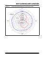
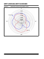
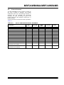


![Stealth Protect Series catalogue 2011_We[...]](http://vs1.manualzilla.com/store/data/005809212_1-caf297493bfcf938dba2b64bb0d79842-150x150.png)