1
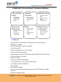
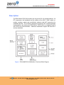
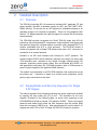
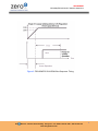
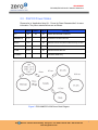
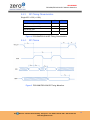
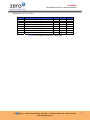
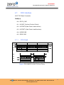
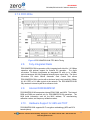
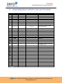
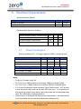
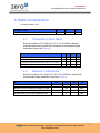
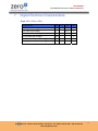
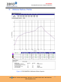
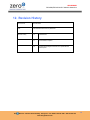
The 4th Age of Wireless™ ZG2100M/ZG2101M Wi-Fi Module Datasheet Preliminary Revision 2.2 PRELIMINARY ZG2100M/ZG2101M Wi‐Fi Modules Datasheet 2.4GHz 802.11b Low Power Transceiver Module Utility and Smart Energy Consumer Electronics Thermostats Smart Meters White Goods HVAC Remote Device Management Location and Asset Tracking Automotive Code Update Industrial Controls Remote Control Internet Radio Home Security Toys Retail - POS Terminals Wireless Price Tags Digital Remote Signage - Chemical Sensors HVAC Security Systems M2M Communication Medical, Fitness, and Healthcare - Glucose Meters Fitness Equipment Patient Asset Tracking Features Single-chip 802.11B including MAC, baseband, RF and power amplifier Data Rate: 1 & 2 Mbps 802.11B/G and 802.11n draft 2.0 compatible Low power operation API for embedded markets, no OS required PCB or external antenna options Hardware support for AES and RC4 based ciphers (WEP, WPA, WPA2 security) SPI slave interface with interrupt Single 3.3V supply 21mm x 31mm 36-pin Dual Flatpack FCC Certified (USA, FCC ID: W7O-ZG2100-ZG2101) IC Certified (IC: 8248A-G21ZEROG) Wi-Fi Certified RoHS and CE compliant Fully compliant with European Market and meet the R&TTE Directive for Radio Spectrum Serial trace interface (UART) Zero Wireless · 255 San Geronimo Way · Sunnyvale · CA · 94085 · 408 738 7600 · 408 738 7601 fax www.zerogwireless.com 2 PRELIMINARY ZG2100M/ZG2101M Wi‐Fi Modules Datasheet Description The ZG2100M & ZG2101M modules are low-power 802.11b implementations. All RF components, the baseband and the entirety of the 802.11 MAC reside onmodule, creating a simple and cost-effective means to add Wi-Fi connectivity for embedded devices. The module(s) implement a high-level API, simplifying design implementation and allowing the ZG2100M or ZG2101M to be integrated with 8and 16-bit host microcontrollers. Hardware accelerators support the latest Wi-Fi security standards. Figure 1 ZG2100M/ZG2101M Modules: Functional Block Diagram Zero Wireless · 255 San Geronimo Way · Sunnyvale · CA · 94085 · 408 738 7600 · 408 738 7601 fax www.zerogwireless.com 2 PRELIMINARY ZG2100M/ZG2101M Wi‐Fi Modules Datasheet Table of Contents 1. Key Feature ............................................................................................................................. 4 2. Detailed Description................................................................................................................. 5 2.1. Overview ................................................................................................................ 5 2.2. Supply Blocks and Boot-Up Sequence for Single 3.3V Supply ............................. 5 2.3. ZG2100 Power States ........................................................................................... 7 2.4. JTAG Interface....................................................................................................... 8 2.5. Serial Interface for Trace ....................................................................................... 8 2.6. SPI Interface .......................................................................................................... 8 2.6.1. SPI Slave Interface with Interrupt for Host Operation ................................. 8 2.6.2. Host-Control SPI Interface ........................................................................... 8 2.6.3. SPI Timing Characteristics ........................................................................ 10 2.6.4. SPI Timing ................................................................................................. 10 2.6.5. SPI Register Access .................................................................................. 12 2.7. FIFO Interface...................................................................................................... 13 2.7.1. FIFO Read ................................................................................................. 13 2.7.2. FIFO Write ................................................................................................. 14 2.8. Fully-Integrated Radio ......................................................................................... 14 2.9. Internal ROM/RAM/NVM ..................................................................................... 14 2.10. Hardware Support for AES and TKIP .................................................................. 14 3. ZG2100M/ZG2101M Pin-Out and Function .......................................................................... 15 4. Package Information .............................................................................................................. 17 5. 4.1. Module Drawing ................................................................................................... 17 4.2. Module Layout Guidelines ................................................................................... 18 Electrical Characteristics ....................................................................................................... 21 5.1. 6. Power Consumption ............................................................................................ 21 Radio Characteristics ............................................................................................................ 22 6.1. Transmitter 2.4GHz Band .................................................................................... 22 6.2. Receiver 2.4GHz Band ........................................................................................ 22 7. Digital Electrical Characteristics ............................................................................................ 23 8. Module Reflow Profile ............................................................................................................ 24 9. Ordering Information .............................................................................................................. 25 10. Limitations 25 11. Regulatory Notes ................................................................................................................... 26 Zero Wireless · 255 San Geronimo Way · Sunnyvale · CA · 94085 · 408 738 7600 · 408 738 7601 fax www.zerogwireless.com 3 PRELIMINARY ZG2100M/ZG2101M Wi‐Fi Modules Datasheet 1. Key Features Ease of Software Development • • • • • • Simple API suited for embedded market Targeted for low resource host processors Entire MAC integrated on-chip Serialized MAC address, each device comes with an unique MAC address in range 001EC0xxxxxx Wireless driver library provides all required control of device Simple usage model, no requirement for OS Low Power Operation • • Low power, 250uA sleep mode with fast wake up, 0.1uA hibernate, Sleep power state managed by ZG2100, enabling low average power while maintaining AP association without host control RF • • • • • • • Integrated PA Support for external PA for high RF output power applications Power output +10dBm typical at antenna Power output programmable from +0dBm to meet varying application needs Min RX sens.of-91dBm @ 1MB/Sec. at antenna Integrated PCB antenna (ZG2100M) Support for external antenna available (ZG2101M) Low External Component Count • • • Fully integrated RF frequency synthesizer Single external crystal is needed, with no external caps , as a source for reference clock Single 3.3V supply with internal built in 1.8V regulator Wi-Fi & Regulatory • • • Supports 1Mbps & 2Mbps and module-based solutions are “Wi-Fi certified” for 802.11b Hardware support for AES, and RC4 based ciphers (WEP, WPA, WPA2 security) FCC Certified (USA, FCC ID: W7O-ZG2100-ZG2101), IC Certified (IC: 8248A-G21ZEROG), Wi-Fi Certified, RoHS and CE compliant, and fully compliant with European Market and meet the R&TTE Directive for Radio Spectrum Zero Wireless · 255 San Geronimo Way · Sunnyvale · CA · 94085 · 408 738 7600 · 408 738 7601 fax www.zerogwireless.com 4 PRELIMINARY ZG2100M/ZG2101M Wi‐Fi Modules Datasheet 2. Detailed Description 2.1. Overview The ZG2100 single-chip 802.11b transceiver includes MAC, baseband, RF and power amplifier, and built in hardware support for AES, and TKIP (WEP, WPA, WPA2 security). The device has an API targeted for embedded markets so an operating system is not required for operation. There is a fully integrated radio ideal for 1 & 2Mbps operation with optional support for external PA and antenna switch operation. The ZG2100M modules incorporate the ZeroG ZG2100 single chip 802.11b transceiver with all associated RF components, crystal oscillator, and bypass and bias passives along with a printed antenna to provide a fully integrated Wi-Fi I/O solution controllable from an 8 or 16-bit processor. The ZG2101M module is similar but bypasses the on-board PCB antenna and uses a U.FL connector for connection to an external antenna. Interface is via SPI slave interface with interrupt for HOST operation. The modules support RS232 serial interfaces (requires level shifter) for debug and JTAG boundary scan. Operation is via a single 3V supply utilizing internal 1.8V regulator, supporting various power states, such as hibernate and SLEEP, for end applications long battery life. ZG2100M contains a built in PCB antenna for ease of system integration and significant BOM reduction. The module is manufactured on an FR4 PCB substrate, with components on the top surface only. Connection is made as a surface mount component via flat pack (no pin) connections on two sides. 2.2. Supply Blocks and Boot-Up Sequence for Single 3.3V Supply The internal regulators for the digital and analog core power supplies are enabled by keeping the chip enable pin (CE_N) low. The waveforms for the core supplies, illustrated on the following page, as shown when powering up the ZG2100M/ZG2101M with a nominal 3.3V applied to VDD33. There is an internal power-on-reset detect which starts the boot sequence from the internal ROM when the core supply (VDD18) is up. After approximately 50 ms from when 3.3V supplies are within 10% of the 3.3V target, the ZG2100 is ready for operation. Zero Wireless · 255 San Geronimo Way · Sunnyvale · CA · 94085 · 408 738 7600 · 408 738 7601 fax www.zerogwireless.com 5 PRELIMINARY ZG2100M/ZG2101M Wi‐Fi Modules Datasheet Figure 2 ZG2100M/ZG2101M ROM Boot Sequence Timing Zero Wireless · 255 San Geronimo Way · Sunnyvale · CA · 94085 · 408 738 7600 · 408 738 7601 fax www.zerogwireless.com 6 PRELIMINARY ZG2100M/ZG2101M Wi‐Fi Modules Datasheet 2.3. ZG2100 Power States Please refer to “Application Note 101 - Power-Up Reset Characteristics” for more information. The power state definitions are as follows: OFF VDD33 VDD18 CE_N 0V 0V 0V Circuitry Power disconnected to ZG2100 HIBERNATE 3.3V 3.3V SLEEP 3.3V 0V Reference clock and internal bias circuitry are ON RX ON 3.3V 0V Receive circuits are ON TX ON 3.3V 0V Transmit circuits are ON STANDBY All internal circuitries are OFF Transition State Only Figure 3 ZG2100M/ZG2101M Power State Diagram Zero Wireless · 255 San Geronimo Way · Sunnyvale · CA · 94085 · 408 738 7600 · 408 738 7601 fax www.zerogwireless.com 7 PRELIMINARY ZG2100M/ZG2101M Wi‐Fi Modules Datasheet 2.4. JTAG Interface Joint Test Action Group (JTAG) is the common name used for the IEEE 1149.1 standard entitled Standard Test Access Port and Boundary-Scan Architecture for test access ports used for testing printed circuit boards using boundary scan. ZG2100M/ZG2101M supports JTAG boundary scan. JTAG_EN and JTAG_RST_N need to be driven HIGH to enable JTAG mode. 2.5. Serial Interface for Trace ZG2100M/ZG2101M incorporates Transmitted Data pin (UART0_TX) and Received Data pin (UART0_RX) for serial testing purposes. These pins can be connected to commercially available RS-232 line drivers/ receivers with appropriate external level shifters. The ZG2100 serial interface is fully tested at 115200 bits/seconds baud rate with RS232/UART interface applications. 2.6. SPI Interface 2.6.1. SPI Slave Interface with Interrupt for Host Operation The slave Serial Peripheral Interface Bus (SPI) is used to interface with the HOST. The slave SPI interface works with ZG2100M/ZG2101M Interrupt line (INT_NX). When data is available for the HOST during operation, the INT_NX line is asserted low by ZG2100. The INT_NX line is de-asserted high, by ZG2100M/ZG2101M, after the data is transferred to the HOST SPI buffer. The SPI CLK Speed can be up to 25MHz. 2.6.2. Host-Control SPI Interface The slave SPI interface implements the [CPOL=0; CPHA=0] and [CPOL=0; CPHA=1] modes (0 and 3) of operation. That is, data is clocked in on the first rising edge of the clock after Chip Select goes valid. Data on the bus is required to be big endian, with most significant bit on the bus first and least significant bit going last. There are two decode regions. One for register access and one for a FIFO interface. Operation for both regions is shown below. The INT_NX signal allows interrupts to be signaled to the host device. Zero Wireless · 255 San Geronimo Way · Sunnyvale · CA · 94085 · 408 738 7600 · 408 738 7601 fax www.zerogwireless.com 8 PRELIMINARY ZG2100M/ZG2101M Wi‐Fi Modules Datasheet As an example of any 32-bit register access, suppose a write to register 0xF0_0F18 is desired: 1. 2. 3. 4. 5. Write to host register 0x38 with addr[31:16] (0x00f0). 24 bit transaction. Write to host register 0x39 with addr[15:0] (0x0F18). 24 bit transaction. Write to host register 0x3a with data[31:16]. 24 bit transaction. Write to host register 0x3b with data[15:0]. 24 bit transaction. Write to host register 0x37 with a byte that has the following pattern: 8 bit transaction a. [7:4] byte enables (active high for the valid bytes that you want to write in steps 3 and 4). b. [3:0] - 4’b0001 -> activate write to register For a read of 0xF0_0D00: 1. Write to host register 0x38 with addr[31:16] (0x00F0). 24 bit transaction. 2. Write to host register 0x39 with addr[15:0] (0x0F18). 24 bit transaction. 3. Write to host register 0x37 with a byte that has the following pattern: 8 bit transaction a. [7:4] byte enables (active high for the valid bytes that you want to read in steps 1 and 2). b. [3:0] - 4’b0011 -> active read of register 4. Read host register 0x3a to get data [31:24] 24 bit transaction 5. Read host register 0x3b to get data [15:0] 24 bit transaction Each of the steps above is a single SPI transaction; the chip select (CE_N) is active low during each step. Zero Wireless · 255 San Geronimo Way · Sunnyvale · CA · 94085 · 408 738 7600 · 408 738 7601 fax www.zerogwireless.com 9 PRELIMINARY ZG2100M/ZG2101M Wi‐Fi Modules Datasheet 2.6.3. SPI Timing Characteristics Single VCC =3.3V (+/-10%) Characteristic Min SPI, Data setup to falling clock 1 ns SPI, Data hold from falling clock 1 ns Max SPI SLAVE CLK 25 MHz SPI MASTER CLK 25 MHz Figure 4 ZG2100M/ZG2101M SPI Timing Characteristics 2.6.4. SPI Timing Figure 5 ZG2100M/ZG2101M SPI Timing Waveform Zero Wireless · 255 San Geronimo Way · Sunnyvale · CA · 94085 · 408 738 7600 · 408 738 7601 fax www.zerogwireless.com 10 PRELIMINARY ZG2100M/ZG2101M Wi‐Fi Modules Datasheet Single VCC = 3.3V (+/-10%) Symbol Tsck Tcs Tcss Tcsh Tsetup Thold Tvalid Tho Parameter SCK Clock Period CS High Time CS Setup Time CS Hold Time Data In Setup Time Data In Hold Time Output Valid Output Hold Time Min 40 ns 50 ns 50 ns 50 ns 10 ns 10 ns Typ 0 Max 15 ns 15 ns Figure 6 ZG2100M/ZG2101M SPI Timing Data Zero Wireless · 255 San Geronimo Way · Sunnyvale · CA · 94085 · 408 738 7600 · 408 738 7601 fax www.zerogwireless.com 11 PRELIMINARY ZG2100M/ZG2101M Wi‐Fi Modules Datasheet 2.6.5. SPI Register Access Figure 7 ZG2100M/ZG2101M SPI Register Timing F is a select between FIFO space and register space. If this bit is a 1, the data FIFO space is selected. If this bit is a 0, the register address space is selected. R is the Read/Write bit. If this bit is a 1, the operation is a read. If this bit is a 0, the operation is a write ADDR0 is the starting address for the transaction. This value is only used for register accesses and is ignored during FIFO accesses. WDATAn is the write data byte. This is only used from write operations and is ignored during read operations. RDATAn is the read data byte. This is always valid for both, read and write operations. If contains the current value of any register location. HOST_INTR is the 8 bit interrupt register. Zero Wireless · 255 San Geronimo Way · Sunnyvale · CA · 94085 · 408 738 7600 · 408 738 7601 fax www.zerogwireless.com 12 PRELIMINARY ZG2100M/ZG2101M Wi‐Fi Modules Datasheet 2.7. FIFO Interface HOST FIFO Basic Commands FCMD[2:0] 0x0 – RFIFO_CMD 0x1 – WCONT (Continue Previous Packet) 0x2 – WSTART0 (Start Packet, head/continue) 0x3 – WSTART1 (Start Packet, head0/continue) 0x4 – WEND CMD 0x5 – REND CMD 2.7.1. FIFO Read Figure 8 ZG2100M/ZG2101M FIFO Read Timing Zero Wireless · 255 San Geronimo Way · Sunnyvale · CA · 94085 · 408 738 7600 · 408 738 7601 fax www.zerogwireless.com 13 PRELIMINARY ZG2100M/ZG2101M Wi‐Fi Modules Datasheet 2.7.2. FIFO Write Figure 9 ZG2100M/ZG2101M FIFO Write Timing 2.8. Fully-Integrated Radio ZG2100M/ZG2101M incorporates a fully integrated radio Ideal for 1 & 2 Mbps operation with optional support for external PA operation. The direct conversion TX design incorporates an integrated PA, with up to +10dBm typical at antenna, and fully integrated internal power control loop. The direct conversion RX chain utilizes Automatic Gain Control that allows ZG2100M/ZG2101M to receive with a minimum input Level sensitivity (1Mbps @ <8% PER) of -91 dBm typical at the antenna. The ZG2100M/ZG2101M only needs an external crystal for a reference clock. 2.9. Internal ROM/RAM/NVM ZG2100M/ZG2101M incorporates internal ROM, RAM, and NVM. The internal ROM and RAM are reserved only for ZG2100M/ZG2101M operations. The NVM holds information such as the MAC address, TX manufacturing calibration values, and frequency calibration values. 2.10. Hardware Support for AES and TKIP ZG2100M/ZG2101M supports Wi-Fi encryption methodology (AES and RC4 based ciphers). Zero Wireless · 255 San Geronimo Way · Sunnyvale · CA · 94085 · 408 738 7600 · 408 738 7601 fax www.zerogwireless.com 14 PRELIMINARY ZG2100M/ZG2101M Wi‐Fi Modules Datasheet 3. ZG2100M/ZG2101M Pin-Out and Function Pins Name GND 1 VDD18 2 JTAG_TDO 3 JTAG_TCK 4 JTAG_TMS 5 JTAG_TDI 6 RST_N 7 DNC 8 9 JTAG_RST_N JTAG_EN 22 23 24 25 26 27 28 29 30 31 32 33 34 35 36 DNC SCS_N VDD18 GND UART_RX UART_TX GND VDD33 GND VDD18 SDO INT_NX SCK SDI GND Required Bias H Constant drive H H Constant drive Constant drive GND VDD18 DNC DNC DNC DNC RES VDD33 GND GND CE_N 10 11 12 13 14 15 16 17 18 19 20 21 Internal Pull-down Description Ground See below JTAG data out JTAG Clock in JTAG Mode in JTAG data in Chip reset in Do Not Connect JTAG Reset in, pulling this pin low will keep JTAG idle (reset) Ground See below Do Not Connect Do Not Connect Do Not Connect Do Not Connect FLASH Write Protect. See below. 3.3V Power Ground Ground Chip enable in JTAG Enable in, this pin needs to be high for Boundary Scan use L Constant drive H Pull-up Constant drive Constant drive Do Not Connect Serial chip select from host (input) See below Ground Debug Serial in Debug Serial out Ground 3.3V Power Ground See below Serial data out to host Interrupt to host (output) Serial clock in from host Serial data in from host Ground Zero Wireless · 255 San Geronimo Way · Sunnyvale · CA · 94085 · 408 738 7600 · 408 738 7601 fax www.zerogwireless.com 15 PRELIMINARY ZG2100M/ZG2101M Wi‐Fi Modules Datasheet Notes: 1. VDD18 is an internally used supply rail. DO NOT USE these pins to drive other components. 2. Signals that note “Constant drive” must either be constantly driven by the host, or have a pullup or pulldown in case the host is likely to tristate the signal during power down modes. The constant drive is used to ensure defined operation of the part and to minimize leakage current during low power modes. Please see the AN102 for further information and requirements for low power operation. 3. RES is used as write-protect for the internal module SPI Flash. For production use, this pin should be grounded or pulled low. Pulling low with host control will enable in-field FLASH updates. For prototype development, this pin may be pulled high to allow for reprogramming. Zero Wireless · 255 San Geronimo Way · Sunnyvale · CA · 94085 · 408 738 7600 · 408 738 7601 fax www.zerogwireless.com 16 PRELIMINARY ZG2100M/ZG2101M Wi‐Fi Modules Datasheet 4. Package Information 4.1. Module Drawing Figure 10 ZG2100M Module Physical Dimensions Figure 11 ZG2101M Module Physical Dimensions Zero Wireless · 255 San Geronimo Way · Sunnyvale · CA · 94085 · 408 738 7600 · 408 738 7601 fax www.zerogwireless.com 17 PRELIMINARY ZG2100M/ZG2101M Wi‐Fi Modules Datasheet Figure 12 ZG2100M/ZG2101M Module Layout Pad Dimensions 4.2. Module Layout Guidelines Figure 13 ZG2100M "Keep Out" Areas Zero Wireless · 255 San Geronimo Way · Sunnyvale · CA · 94085 · 408 738 7600 · 408 738 7601 fax www.zerogwireless.com 18 PRELIMINARY ZG2100M/ZG2101M Wi‐Fi Modules Datasheet In addition to the guidelines in Figure 13, note the following suggestions: ZG2100M and ZG2101M • Bypass capacitors for 3.3V should be close to pin 17. • Routing under the module except for limits shown in Figure 10 is acceptable, if they are solder-masked. • Do not route any nets to VDD18 • Do not use VDD18 to source any external nets. • Never place the antenna very close to metallic objects. ZG2100M onboard PCB antenna specific • In the final product, ensure that any wiring or other components do not get too close to the antenna or run parallel to the length of the antenna trace. • The antenna will need a reasonable ground plane area on the mother board area to be efficient. • Do not use a metallic or metalized plastic for the enclosure. • Plastic enclosure keep away dimension, from the antenna in any orientation, will be provided after module antenna characterizations. • To maintain the efficiency and impedance for ZG2100M PCB antenna, designer should keep conductors and dielectrics, which are more than 0.5 mm thick, 15 mm from the antenna in all directions. Zero Wireless · 255 San Geronimo Way · Sunnyvale · CA · 94085 · 408 738 7600 · 408 738 7601 fax www.zerogwireless.com 19 PRELIMINARY ZG2100M/ZG2101M Wi‐Fi Modules Datasheet Module Use Schematic Figure 14 ZG2100M/ZG2101M Module Use Schematic Figure 15 ZG2101M Antenna Placement Zero Wireless · 255 San Geronimo Way · Sunnyvale · CA · 94085 · 408 738 7600 · 408 738 7601 fax www.zerogwireless.com 20 PRELIMINARY ZG2100M/ZG2101M Wi‐Fi Modules Datasheet 5. Electrical Characteristics Absolute Maximum Ratings: Rating Storage Temperature Min -40C Max +125C 3V supply (VDD_3.3) 0V 4.2V Recommended Operating Conditions: Operating Condition Ambient Temperature Range, commercial parts Min 0C Typ Temperature Range, Extended parts -20C +85C Temperature Range, Industrial parts -40C +85C 3V supply (VDD_3.3) 2.97V 3.30V Max +70C 3.63V 5.1. Power Consumption Nominal conditions: 25C, 3.3V supply applied to VDD33, commercial parts. Power Conservation Modes Min Typ Max Unit Hibernate, CE_N=3.3v 0.1 uA Sleep 250 uA Standby (transitional power state) 10 mA Core Supply Rx On, Receive Min Irx, -83dBm Typ Max Unit 85 mA Tx On, Transmit Itx, +0dBm 165 mA Tx On, Transmit Itx, +10dBm 230 mA Notes: 1. For Rx On, RX chain is fully ON. 2. For Tx On, Pout= 0dBm (measured at antenna); 2Mb/Sec.modulated signal 3. For Tx On, Pout= +10dBm (measured at antenna); 2Mb/Sec.modulated signal 4. 3.3V Current Consumption values represent Typical Peak currents. Wi-Fi protocol is such that current draw occurs at less than 100% duty cycle. Tx is dependent on such criteria as transmit power setting, and transmit data rate and bandwidth being used. Rx is affected by connectivity distance. 5. Contact factory for Extended and Industrial part characteristics. All characteristics in this specification are for commercial temperature rated parts only. Zero Wireless · 255 San Geronimo Way · Sunnyvale · CA · 94085 · 408 738 7600 · 408 738 7601 fax www.zerogwireless.com 21 PRELIMINARY ZG2100M/ZG2101M Wi‐Fi Modules Datasheet 6. Radio Characteristics Nominal conditions: 25C. Frequency range Min Max Unit F_LO 2412 2484 MHz 6.1. Transmitter 2.4GHz Band Nominal conditions: 25C, Single VCC =3.3V, Flo=2437MHz; 2Mb/Sec. modulated signal duty cycled at 95% measured at recommended single ended balun output (see Figure 8). Min TX Typ Max Unit Average Pout (Transmit spectrum mask Compliant) +10 dBm Average Pout gain step resolution from +5 to +10 dBm 0.5 dB Average Pout gain step resolution from -5 to +5 dBm 1.0 dB Average Pout settled variation 6.2. -0.5 0.5 dB Receiver 2.4GHz Band Nominal conditions: 25C, Single VCC =3.3V, Flo=2437MHz; measured at recommended single ended balun input (see Figure 8). Min RX Typ Max Unit RX Min Input Level Sensitivity, 1Mbps, 8% PER -91 dBm RX Min Input Level Sensitivity, 2Mbps, 8% PER -88 dBm RX Max Input Level (Power), 1Mbps, 8% PER -4 dBm RX Max Input Level (Power), 2Mbps,8% PER -4 dBm Zero Wireless · 255 San Geronimo Way · Sunnyvale · CA · 94085 · 408 738 7600 · 408 738 7601 fax www.zerogwireless.com 22 PRELIMINARY ZG2100M/ZG2101M Wi‐Fi Modules Datasheet 7. Digital Electrical Characteristics Single VCC =3.3V (+/-10%) Characteristic Min VIL (Input Low Voltage) -0.3 VIH (Input High Voltage) 2 Typ VOL (Output Low Voltage) VOH (Output High Voltage) 2.4 Max Unit 0.8 V Vcc*1.1 V 0.4 V V IOL (Low Level Output Current @ VOL Max) 8.5 mA IOH (High Level Output Current @ VOH Min) 15.4 mA Zero Wireless · 255 San Geronimo Way · Sunnyvale · CA · 94085 · 408 738 7600 · 408 738 7601 fax www.zerogwireless.com 23 PRELIMINARY ZG2100M/ZG2101M Wi‐Fi Modules Datasheet 8. Module Reflow Profile Figure 16 ZG2100M/ZG2101M Module Reflow Setpoints Zero Wireless · 255 San Geronimo Way · Sunnyvale · CA · 94085 · 408 738 7600 · 408 738 7601 fax www.zerogwireless.com 24 PRELIMINARY ZG2100M/ZG2101M Wi‐Fi Modules Datasheet 9. Ordering Information DEVICE DESCRIPTION COMMENT ORDERING NUMBER Module Module Version using PCB antenna Version using external antenna ZG2100MCC3 ZG2101MCC3 Module Extended grade Contact factory Module Industrial grade Contact factory 10. Limitations THIS DEVICE AND ASSOCIATED SOFTWARE ARE NOT DESIGNED, MANUFACTURED OR INTENDED FOR USE OR RESALE FOR THE OPERATION OF NUCLEAR FACILITIES, THE NAVIGATION, CONTROL OR COMMUNICATION SYSTEMS FOR AIRCRAFT OR OTHER TRANSPORTATION, AIR TRAFFIC CONTROL, LIFE SUPPORT OR LIFE SUSTAINING APPLICATIONS, WEAPONS SYSTEMS, OR ANY OTHER APPLICATION IN A HAZARDOUS ENVIRONMENT, OR REQUIRING FAIL-SAFE PERFORMANCE, OR IN WHICH THE FAILURE OF PRODUCTS COULD LEAD DIRECTLY TO DEATH, PERSONAL INJURY, OR SEVERE PHYSICAL OR ENVIRONMENTAL DAMAGE (COLLECTIVELY, "HIGH RISK APPLICATIONS"). YOU AGREE AND ACKNOWLEDGE THAT YOU HAVE NO LICENSE TO, AND SHALL NOT (AND SHALL NOT ALLOW A THIRD PARTY TO) USE THE TECHNOLOGY IN ANY HIGH RISK APPLICATIONS, AND LICENSOR SPECIFICALLY DISCLAIMS ANY WARRANTY REGARDING, AND ANY LIABILITY ARISING OUT OF, HIGH RISK APPLICATIONS. Zero Wireless · 255 San Geronimo Way · Sunnyvale · CA · 94085 · 408 738 7600 · 408 738 7601 fax www.zerogwireless.com 25 PRELIMINARY ZG2100M/ZG2101M Wi‐Fi Modules Datasheet 11. Regulatory Notes Federal Communication Commission Interference Statement This equipment has been tested and found to comply with the limits for a Class B digital device, pursuant to Part 15 of the FCC Rules. These limits are designed to provide reasonable protection against harmful interference in a residential installation. This equipment generates uses and can radiate radio frequency energy and, if not installed and used in accordance with the instructions, may cause harmful interference to radio communications. However, there is no guarantee that interference will not occur in a particular installation. If this equipment does cause harmful interference to radio or television reception, which can be determined by turning the equipment off and on, the user is encouraged to try to correct the interference by one of the following measures: - Reorient or relocate the receiving antenna. - Increase the separation between the equipment and receiver. - Connect the equipment into an outlet on a circuit different from that to which the receiver is connected. - Consult the dealer or an experienced radio/TV technician for help. FCC Caution: To assure continued compliance, (example - use only shielded interface cables when connecting to computer or peripheral devices). Any changes or modifications not expressly approved by the party responsible for compliance could void the user's authority to operate this equipment. This device complies with Part 15 of the FCC Rules. Operation is subject to the following two conditions: (1) This device may not cause harmful interference, and (2) this device must accept any interference received, including interference that may cause undesired operation. IMPORTANT NOTE: FCC & IC Radiation Exposure Statement: This equipment complies with FCC & IC radiation exposure limits set forth for an uncontrolled environment. This equipment should be installed and operated with minimum distance 20cm between the radiator & your body. This transmitter must not be co-located or operating in conjunction with any other antenna or transmitter. This device is intended only for OEM integrators under the following conditions: 1) The antenna must be installed such that 20 cm is maintained between the antenna and users, and 2) The transmitter module may not be co-located with any other transmitter or antenna. As long as 2 conditions above are met, further transmitter test will not be required. However, the OEM integrator is still responsible for testing their end-product for any additional compliance requirements required with this module installed (for example, digital device emissions, PC peripheral requirements, etc.). Zero Wireless · 255 San Geronimo Way · Sunnyvale · CA · 94085 · 408 738 7600 · 408 738 7601 fax www.zerogwireless.com 26 PRELIMINARY ZG2100M/ZG2101M Wi‐Fi Modules Datasheet IMPORTANT NOTE: In the event that these conditions cannot be met (for example certain laptop configurations or co-location with another transmitter), then the FCC & IC authorizations are no longer considered valid and the FCC & IC IDs cannot be used on the final product. In these circumstances, the OEM integrator will be responsible for reevaluating the end product (including the transmitter) and obtaining separate FCC & IC authorizations. End Product Labeling This transmitter module is authorized only for use in device where the antenna may be installed such that 20 cm may be maintained between the antenna and users (for example access points, routers, wireless ADSL modems, and similar equipment). The final end product must be labeled in a visible area with the following: “Contains FCCID: W7OZG2100-ZG2101 & IC: 8248A-G21ZEROG”. IC Certification — Canada The labeling requirements for Industry Canada are similar to those of the FCC. A visible label on the outside of the final product must display the IC labeling. The user is responsible for the end product to comply with IC ICES-003 (Unintentional radiators) Manual Information That Must be Included The user’s manual for end users must include the following in-formation in a prominent location. IMPORTANT NOTE: To comply with FCC & IC RF exposure compliance requirements, the antenna used for this transmitter must be installed to provide a separation distance of at least 20 cm from all persons and must not be co-located or operating in conjunction with any other antenna or transmitter. Zero Wireless · 255 San Geronimo Way · Sunnyvale · CA · 94085 · 408 738 7600 · 408 738 7601 fax www.zerogwireless.com 27 PRELIMINARY ZG2100M/ZG2101M Wi‐Fi Modules Datasheet 12. Revision History Document ID DS-ZG2100M Title ZG2100M-ZG2101M WiFi Chip Datasheet Revision History 1.0 Initial Release 2.1 Characterization Updates 2.2 Updated with SPI/digital information and updated Module Reflow profile Zero Wireless · 255 San Geronimo Way · Sunnyvale · CA · 94085 · 408 738 7600 · 408 738 7601 fax www.zerogwireless.com 28