1
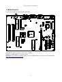
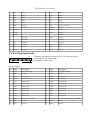
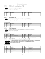
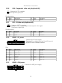
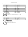
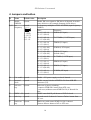
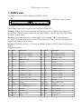
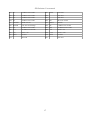
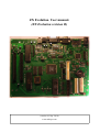
ZX Evolution. User manual.
(ZX Evolution revision B)
(version 19. Sep. 2010)
www.nedopc.com
ZX Evolution. User manual
Table of contents
1 Introduction......................................................................................................................................3
2 Board layout.....................................................................................................................................4
3 Connectors........................................................................................................................................5
3.1 X1. Floppy drive.......................................................................................................................5
3.2 X2. IDE.....................................................................................................................................6
3.3 X3. IO port and audio...............................................................................................................6
3.4 X4. JTAG for EP1K50Q208.....................................................................................................7
3.5 X5. AVR ISP for ATMEGA128...............................................................................................7
3.6 X6. RS232 communication.......................................................................................................8
3.7 X7. VGA...................................................................................................................................8
3.8 X8. S-Video out........................................................................................................................8
3.9 X9. Composite video out..........................................................................................................9
3.10 X10. 3.5 Audio out..................................................................................................................9
3.11 X11. PS/2 keyboard and mouse..............................................................................................9
3.12 X12. Joystick and original ZX keyboard................................................................................9
3.13 X13. RGB video out.............................................................................................................10
3.14 X14. AVR JTAG for ATMEGA128......................................................................................10
3.15 X15. Tape in/out....................................................................................................................11
3.16 X16. Audio out (duplicate X10)............................................................................................11
3.17 X17. Audio in........................................................................................................................11
3.18 X18. Reserved.......................................................................................................................11
3.19 X19. RS232 communication (duplicate X6).........................................................................11
3.20 X20. Composite video out (duplicate X9)............................................................................12
3.21 X21. S-Video out (duplicate X8)..........................................................................................12
3.22 PWR1. AT power..................................................................................................................12
3.23 PWR2. ATX power...............................................................................................................13
3.24 PWR3. Power........................................................................................................................13
3.25 GB1. Battery holder..............................................................................................................13
4 Jumpers and button.........................................................................................................................15
5 ZXBUS slots...................................................................................................................................17
6 Installation ZX Evolution to ATX/miniATX case..........................................................................19
7 Installation ZX Evolution to AT case.............................................................................................20
8 Appendix 1. Ribbon cable for floppy drives..................................................................................21
2
ZX Evolution. User manual
1 Introduction
ZX Evolution is Spectrum compatible computer. Computer based on programmable logic device
Altera EP1K50Q208 and has flexible architecture, but board content original main chips (Z80,
sound coprocessor, floppy controller).
ZX Evolution board designed by miniATX standard for easy installation to miniATX or ATX case.
Main features:
•
Z80 on 3.5MHz (standard)/7 MHz (turbo mode) without wait circles;
•
4 MBytes RAM, 512KBytes ROM (flash ROM);
•
MiniATX form factor, support ATX or AT power supply;
•
2 ZXBUS slots;
•
Peripheral controller ATMEGA128;
•
PS/2 keyboard/mouse interface;
•
IDE interface [parallel ATA] (one channel, up to 2 devices on master/slave mode);
•
SD(HC) memory card interface;
•
Floppy disk interface based on WDC1793 (support up to 4 drives);
•
RS232 interface;
•
Realtime/Calendar (RTC);
•
Sound interfaces: AY38910/YM2149F, beeper, pwm;
•
Joystick and mechanical (original) keyboard interface;
•
Tape interface (input/output);
•
RGB video out (SCART compatible);
•
Integrated PAL coder on CXA1645M/CXA2075M (composite and S-Video output);
•
VGA (scan doubler).
3
ZX Evolution. User manual
2 Board layout
Layout of components and connectors on board:
ATMEGA128
D4
Most usable connectors place to ATX cases “window”.
Board use standard ATX or AT power supply.
Warning: Only ZXBUS compatible devices may installed to slot (for example NeoGS sound card:
http://www.nedopc.com/gs/ngs.php ).
4
ZX Evolution. User manual
3 Connectors
3.1 X1. Floppy drive
2
34
1
33
Connector for floppy drive[s] (3.5' or 5.25'). Supported up
to four devices.
First pin have square pad.
Pins description:
№
Name
Description
№
Name
Description
1
GND
Ground
2
Not used
3
GND
Ground
4
Not used
5
KEY
key (no contact)
6
DS3
Select 3 drive (D)
7
GND
Ground
8
IDX
Index
9
GND
Ground
10
DS0
Select 0 drive (A)
11
GND
Ground
12
DS1
Select 1 drive (B)
13
GND
Ground
14
DS2
Select 2 drive (C)
15
GND
Ground
16
MOTON
Motor on
17
GND
Ground
18
DIRC
Direction
19
GND
Ground
20
STEP
Step
21
GND
Ground
22
WD
Write data
23
GND
Ground
24
WG
Write enable
25
GND
Ground
26
TR00
Track 0
27
GND
Ground
28
WP
Write protect
29
GND
Ground
30
RDDATA
Read data
31
GND
Ground
32
SIDE1
Side select
33
GND
Ground
34
Not used
3.2 X2. IDE
2
40
1
39
Connector for IDE (parallel ATA) drives. Supported
up to two drives on master/slave mode.
First pin have square pad.
Pins description:
№
Name
Description
№
Name
Description
1
RESET
Reset
2
GND
Ground
3
D07
Data7
4
D08
Data8
5
D06
Data6
6
D09
Data9
7
D05
Data5
8
D10
Data10
5
ZX Evolution. User manual
9
D04
Data4
10
D11
Data11
11
D03
Data3
12
D12
Data12
13
D02
Data2
14
D13
Data13
15
D01
Data1
16
D14
Data14
17
D00
Data0
18
D15
Data15
19
GND
Ground
20
KEY
KEY (no contact)
Not used
22
GND
Ground
21
23
DIOW
24
GND
Ground
25
DIOR
26
GND
Ground
27
IORDY
28
Not used
29
Not used
30
GND
Ground
31
Not used
32
Not used
Not used
33
DA1
Address1
34
35
DA0
Address0
36
DA2
Address1
37
CS0
Select0
38
CS1
Select
39
DASP
Indicator
40
GND
Ground
3.3 X3. IO port and audio
2
28
1
27
Connector for connect external devices (AY/YM coprocessor
port interface) and audio output.
First pin have square pad.
Pins description:
№
Name
Description
№
Name
Description
1
LOUT
Left audio output
2
ROUT
Right audio output
3
GND
Ground
4
GND
Ground
5
AYA0
Data0 port A
6
AYB0
Data0 port B
7
AYA1
Data1 port A
8
AYB1
Data1 port B
9
AYA2
Data2 port A
10
AYB2
Data2 port B
11
AYA3
Data3 port A
12
AYB3
Data3 port B
13
AYA4
Data4 port A
14
AYB4
Data4 port B
15
AYA5
Data5 port A
16
AYB5
Data5 port B
17
AYA6
Data6 port A
18
AYB6
Data6 port B
19
AYA7
Data7 port A
20
AYB7
Data7 port B
21
+5V
Power +5V
22
+5V
Power +5V
23
RESZ
Reset (Z80 reset line)
24
AY_CLK
AY/YM clock frequency (1.75MHz)
25
GND
Ground
26
GND
Ground
27
GND
Ground
28
GND
Ground
6
ZX Evolution. User manual
3.4 X4. JTAG for EP1K50Q208
2
10
1
9
Connector for programming FPGA EP1K50Q208 via JTAG interface (with
ByteBlasterMV or other programming device).
First pin have square pad.
Pins description:
№
Name
Description
№
Name
Description
1
TCK
Clock
2
GND
Ground
3
TDO
Data output
4
3V3
Power +3.3V
5
TMS
Mode select
6
Not used
Not used
8
Not used
Data input
10
7
9
TDI
GND
Ground
3.5 X5. AVR ISP for ATMEGA128
2
10
1
9
Connector for programming ATMEGA128 via ISP (with ByteBlasterMV or
other programming device).
First pin have square pad.
Pins description:
№
Name
Description
№
Name
Description
1
CK
Clock
2
GND
Ground
3
DO
Data output
4
VCC5
Power +5V
5
RST
Reset
6
Not used
8
EXCLOCK
External clock
Data input
10
GND
Ground
7
9
DI
Not used
3.6 X6. RS232 communication
Communication port used for connection with other computer or
communicating devices (for example modem). Up to 115200BOD
transfer speed.
1 2 3 4 5
6 7 8 9
Pins description:
№
Name
1
Description
№
Not used
6
Name
Description
Not used
2
RXD
Receive data
7
RTS
Request to send
3
TXD
Transmit date
8
CTS
Clear to send
Not used
9
Not used
Ground
Shield
Connected to ground
4
5
GND
7
ZX Evolution. User manual
3.7 X7. VGA
5 4 3 2 1
10
6
15 14 13 12 11
Connector for monitor or TV.
Warning: Monitor or TV must support 50Hz, 31KHz video rate.
Please refer to monitor manual or compatible monitors list:
http://www.nedopc.com/zxevo/zxevo_supported_monitors.pdf .
Pins description:
№
Name
Description
№
Name
Description
1
R
Red
9
2
G
Green
10
GND
Ground
3
B
Blue
11
GND
Ground
4
Not used
12
5
Not used
13
HS
Horizontal synchronization
VS
Vertical synchronization
Not used
Not used
6
GND
Ground
14
7
GND
Ground
15
Not used
8
GND
Ground
Shield
Shield connect to ground
3.8 X8. S-Video out
3
1
Connector for TV or monitor.
Quality of s-video signal is higher than composite video signal.
4
2
Pins description:
№
Name
Description
№
Name
Description
1
GND
Ground
2
GND
Ground
3
C
Chrominance
4
Y
Luminance
3.9 X9. Composite video out
Connector for TV or monitor. Shield connect to ground.
3.10
X10. 3.5 Audio out
Connector for headphone or speaker.
Shield connect to ground.
8
ZX Evolution. User manual
3.11
X11. PS/2 keyboard and mouse
12
10
11
9
8
Connector for PS/2 keyboard and mouse. Keyboard connect into near from
board (bottom) socket. Mouse connect into far from board (top) socket.
Shield connect to ground.
7
6
4
5
3
2
1
Pins description:
№
Name
Description
№
Name
Description
1
DATA
Keyboard data
7
DATA
Mouse data
Not used
8
2
Not used
3
GND
Ground
9
GND
Ground
4
+5V
Power +5V
10
+5V
Power +5V
5
CLK
Keyboard clock
11
CLK
Mouse clock
Not used
12
6
3.12
Not used
X12. Joystick and original ZX keyboard
2
20
1
19
Connector for original ZX keyboard or joystick.
First pin have square pad.
Pins description:
№
Name
1
Description
№
Name
ZXROW0 0 row of original keyboard
2
ZXROW1 1 row of original keyboard
3
ZXROW2 2 row of original keyboard
4
ZXROW3 3 row of original keyboard
5
ZXROW4 4 row of original keyboard
6
ZXROW5 5 row of original keyboard
7
ZXROW6 6 row of original keyboard
8
ZXROW7 7 row of original keyboard
9
RST
Reset
10
ZXCOL4
4 column of original keyboard
11
ZXCOL3
3 column of original keyboard
12
ZXCOL2
2 column of original keyboard
13
ZXCOL1
1 column of original keyboard
14
ZXCOL0
0 column of original keyboard
15
GND
Ground
16
JOYL
Left of joystick
17
JOYR
Right of joystick
18
JOYU
Up of joystick
19
JOYD
Down of joystick
20
JOYF
Fire of joystick
9
Description
ZX Evolution. User manual
3.13
X13. RGB video out
8 7 6 5 4 3 2 1
15 14 13 12 11 10 9
Connector for monitors or TV (via SCART).
Shield connect to ground.
Warning: Some TV not content RGB video inputs on SCART
connector. Please refer to TV user manual.
Pins description:
№
Name
Description
№
Name
Description
1
GND
Ground
9
R
Red
2
GND
Ground
10
G
Green
3
GND
Ground
11
B
Blue
4
CPAL
Composite video out
12
VS
Vertical synchronization
5
GND
Ground
13
CS
Composite synchronization
6
LOUT
Left audio out
14
GND
Ground
7
ROUT
Right audio out
15
VCC
Power +5V
8
HS
Horizontal synchronization
Shield
3.14
Shield connect to ground
X14. AVR JTAG for ATMEGA128
2
10
1
9
Connector for programming ATMEGA128 via JTAG ICT.
First pin have square pad.
Pins description:
№
Name
Description
№
Name
Description
1
TCK
Clock
2
GND
Ground
3
TDO
Data output
4
VCC
Power +5V
5
TMS
Mode select
6
PRGRST
Reset
7
VCC
Power +5V
8
9
TDI
Data input
10
GND
3.15
Not used
Ground
X15. Tape in/out
Connector for tape device.
First pin have square pad.
Pins description:
1
3
2
4
№
Name
Description
№
Name
Description
1
IN
Tape input
2
GND
Ground
3
OUT
Tape output
4
GND
Ground
10
ZX Evolution. User manual
3.16
4 3 2 1
X16. Audio out (duplicate X10)
Connector for headphone or speaker.
First pin have square pad.
Pins description:
№
Name
Description
№
Name
Description
1
LOUT
Left
2
GND
Ground
3
GND
Ground
4
ROUT
Right
3.17
1 2 3 4
X17. Audio in
Connector for external audio sources (for example CDROM).
First pin have square pad.
Pins description:
№
Name
Description
№
Name
Description
1
LIN
Left
2
GND
Ground
3
GND
Ground
4
RIN
Right
3.18
4 3 2 1
X18. Reserved
Connector with reserved pins of ATMEGA128. Reserved for future use.
First pin have square pad.
Pins description:
№
Name
Description
№
Name
Description
1
PE2
PE2 pin on ATMEGA128
2
GND
Ground
3
GND
Ground
4
PE3
PE3 pin on ATMEGA128
3.19
X19. RS232 communication (duplicate X6)
2
10
1
9
Communication port used for connection with other computer or communicating
devices (for example modem). Up to 115200BOD transfer speed.
First pin have square pad.
Pins description:
№
Name
1
Description
№
Name
Description
Not used
2
RXD
Receive data
3
TXD
Transmit data
4
Not used
5
GND
Ground
6
Not used
7
RTS
Request to send
8
Not used
10
9
11
CTS
Clear to send
Not used
ZX Evolution. User manual
3.20
X20. Composite video out (duplicate X9)
Connector for TV or monitor.
First pin have square pad.
2 1
Pins description:
№
Name
Description
№
Name
Description
1
CPAL
Composite video
2
GND
Ground
3.21
1 2 3 4
X21. S-Video out (duplicate X8)
Connector for TV or monitor.
Quality of s-video signal is higher than composite video signal.
First pin have square pad.
Pins description:
№
Name
Description
№
Name
Description
1
Y
Luminance
2
GND
Ground
3
GND
Ground
4
C
Chrominance
3.22
PWR1. AT power
Connector for AT power supply.
Warning: Wires marked black (on P8 and P9) must be
together in center of boards connector.
1
12
Pins:
№
Name
1
№
Name
Description
PWRGOOD Power is good
7
GND
Ground
2
VCC5
Power +5V
8
GND
Ground
3
VCC12
Power +12V
9
Not used
10
VСС5
Power +5V
4
Description
Not used
5
GND
Ground
11
VCC5
Power +5V
6
GND
Ground
12
VCC5
Power +5V
3.23
PWR2. ATX power
1
10
11
20
Connector for ATX power supply.
12
ZX Evolution. User manual
Pins description:
№
Name
Description
№
Name
Description
1
Not used
11
Not used
2
Not used
12
Not used
3
GND
Ground
13
GND
Ground
4
VCC5
Power +5V
14
PS_ON
Power on
5
GND
Ground
15
GND
Ground
6
VCC5
Power +5V
16
GND
Ground
7
GND
Ground
17
GND
Ground
8
PWRGOOD Power is good
18
9
VCC5STBY Standby +5V
19
VCC5
Power +5V
10
VCC12
20
VCC5
Power +5V
3.24
Power +12V
Not used
PWR3. Power
4
3
2
1
Connector for non-standard power supply (+12V, +5V, GND).
Pins description:
№
Name
Description
№
Name
Description
1
VCC5
Power +5V
3
GND
Ground
2
GND
Ground
4
VCC12
Power +12V
3.25
GB1. Battery holder
Holder for RTC battery.
Please use CR2032 batteries (3Volt).
13
ZX Evolution. User manual
4 Jumpers and button
№
Name
Default value
Description
J1
enable
IDERES
opened
Enable IDE reset signal to IDE drives if shorted. It need to
some old drives (for example Samsung 10Gb drives).
J2,J3
set
frequency
opened
Set frequency multiplier of PLL ICS501M (input frequency
14MHz).
State
Frequency
1 3 2
1 3 2
1 - GND
2 - VCC5
J2:3 - S0
J3:3 - S1
J3:1-3 2 (S1=0)
J2:1-3 2 (S0=0)
56MHz (4X input)
J3:1-3 2 (S1=0)
J2:1 3 2 (S0=M)
74.375MHz (5.3125X input)
J3:1-3 2 (S1=0)
J2:1 3-2 (S0=1)
70MHz (5X input)
J3:1 3 2 (S1=M)
J2:1-3 2 (S0=0)
91MHz (6.25X input)
J3:1 3 2 (S1=M)
J2:1 3 2 (S0=M)
28MHz (2X input)
[default value]
J3:1 3 2 (S1=M)
J2:1 3-2 (S0=1)
43.75MHz (3.125X input)
J3:1 3-2 (S1=1)
J2:1-3 2 (S0=0)
84MHz (6X input)
J3:1 3-2 (S1=1)
J2:1 3 2 (S0=M)
42MHz (3X input)
J3:1 3-2 (S1=1)
J2:1 3-2 (S0=1)
112MHz (8X input)
J4
12v enable opened
Enable +12V power supply to slots if shorted.
J5
external
clock
opened
Enable external clock to ATMEGA128 from AVR ISP
connector (X5).
J6
soft reset
key
opened
Soft reset or power switching:
- connect «PWR SW» button from ATX case;
- soft reset (without restart ATMEGA128) if shorted few
time.
J7
HRDY->IP opened
HRDY controlled IP pull-down to GND if closed.
J8
turbo key
opened
Set turbo mode if shorted. Connect «Turbo» button from
AT case.
J9
hard reset
key
opened
Hard reset (with restart ATMEGA128) if shorted.
Connect «Reset» button of AT or ATX case.
14
ZX Evolution. User manual
VD31 HDD Led
Connect «HDD LED» from AT or ATX case.
VD62 PWR Led
Connect «PWR LED» from AT or ATX case.
S13
Hard reset (with restart ATMEGA128).
hard reset
button
1 If set contacts instead VD3 led on board (for example boards from NedoPC).
2 If set contacts instead VD6 led on board (for example boards from NedoPC).
3 Not installed on boards from NedoPC.
15
ZX Evolution. User manual
5 ZXBUS slots
ZX Evolution have two slots compatible to ZXBUS standard.
B31
B1
A31
A1
ZXBUS pin step is 2.54mm.
First pin have square pad. First pin is near to rear side of ATX case.
Warning: ZXBUS cards key must placed to first pins side of slot. If ZXBUS card not have key,
please refer to ZXBUS card user manual. If you install ZXBUS card incorrectly than ZXEvolution
board may be malfunction.
Warning: ZX Evolution developer not guaranteed correct working ZXBUS cards from other
developers. ZX Evolution developer not test ZXBUS cards from other developers. Testing must be
organized by ZXBUS cards developer.
Warning: If ZXBUS card need +12V power on slot than J4 jumper on ZX Evolution board must be
shorted.
Slot pins description:
№
Name
Description
№
Name
Description
A1
A14
14 address line of CPU
B1
A15
15 address line of CPU
A2
A12
12 address line of CPU
B2
A13
13 address line of CPU
A3
+5V
Power +5V
B3
D7
7 data line of CPU
A4
DCDOS
TRDOS enabled
B4
Not used
Not used
B5
Not used
A5
A6
GND
Ground
B6
D0
0 data line of CPU
A7
GND
Ground
B7
D1
1 data line of CPU
Not used
B8
D2
2 data line of CPU
A8
A9
A0
0 address line of CPU
B9
D6
6 data line of CPU
A10
A1
1 address line of CPU
B10
D5
5 data line of CPU
A11
A2
2 address line of CPU
B11
D3
3 data line of CPU
A12
A3
3 address line of CPU
B12
D4
4 data line of CPU
A13
IORQGE
Disable other devices (io catch)
B13
INT
Interrupt
A14
GND
Ground
B14
NMI
Non masked interrupt
A15
CSROMCE Enable ROM selection
B15
HALT
CPU halt
A16
RS
Switch ROM pages
B16
MREQ
CPU memory request
A17
Not used
B17
IORQ
CPU io request
A18
Not used
B18
RD
CPU read data
WR
CPU write data
A19
BUSRQ
CPU bus request
B19
A20
RES
Reset
B20
16
Not used
ZX Evolution. User manual
A21
A7
7 address line of CPU
B21
A22
A6
6 address line of CPU
B22
Not used
A23
A5
5 address line of CPU
B23
Not used
A24
A4
4 address line of CPU
B24
M1
M1 state of CPU
A25
CSROM
ROM selected
B25
RFSH
Refresh
A26
BUSAK
CPU bus acknowledge
B26
A8
8 address line of CPU
A27
A9
9 address line of CPU
B27
A10
10 address line of CPU
A28
A11
11 address line of CPU
B28
+5V
Power +5V
A29
+5V
Power +5V
B29
+12V
Power +12V
A30
GND
Ground
B30
GND
Ground
Not used
B31
A31
17
WAIT
CPU wait
Not used
ZX Evolution. User manual
6 Installation ZX Evolution to ATX/miniATX case
ZX Evolution board designed for easy installing to ATX or miniATX case.
Warning: ZX Evolution not complected with brackets and fixates.
Steps:
1. Set CR2032 battery or compatible to GB1 holder on board.
2. Set board to cases frame. Set frame into case. Connectors (X10, X8, X13, X7, XSD1, X11)
must placed to “window” on rear side of case.
3. Connect cases power supply to PWR2.
4. Connect RES SW (from «Reset» button on case) to J9 (hard reset) on board.
5. Connect PWR SW (from «Power» button on case) to J6 (soft reset) on board.
6. Connect IDE LED (from «Ide» led on case) to VD34 on board (positive contact have square
pad).
7. Connect PWR LED (from «Power» led on case) to VD65 on board (positive contact have
square pad).
8. Set floppy drive(s)6 into case, connect power supply to drive(s) and connect to X1 via ribbon
cable.
Warning: Ribbon cable of floppy drive not compatible with standard PC ribbon cable.
Scheme of ribbon cable see in appendix.
9. Set IDE drive(s)7 into case, connect power supply to drive(s) connect to X2 via ribbon cable.
Warning: Installing two IDE drives may be only in master/slave mode.
4
5
6
7
If set contacts instead VD3 led on board (for example boards from NedoPC).
If set contacts instead VD6 led on board (for example boards from NedoPC).
Floppy drive is not mandatory, ZX Evolution work normally without it.
IDE drive is not mandatory, ZX Evolution work normally without it.
18
ZX Evolution. User manual
7 Installation ZX Evolution to AT case
AT case necessary to prepare:
•
create «window» on rear side of case for ZX Evolution boards connectors;
•
create mounting holes on cases frame accord ZX Evolution board holes.
Warning: ZX Evolution not complected with brackets and fixates.
Steps:
1. Set CR2032 battery or compatible to GB1 holder on board.
2. Set board to cases frame. Set frame into case. Connectors (X10, X8, X13, X7, XSD1, X11)
must placed to “window” on rear side of case.
3. Connect cases power supply to PWR1.
4. Connect RES SW (from «Reset» button on case) to J9 (hard reset) on board.
5. Connect TURBO SW (from «Turbo» button on case) to J8 (turbo key) on board.
6. Connect IDE LED (from «Ide» led on case) to VD38 on board (positive contact have square
pad).
7. Connect PWR LED (from «Power» led on case) to VD69 on board (positive contact have
square pad).
8. Set floppy drive(s)10 into case, connect power supply to drive(s) and connect to X1 via
ribbon cable.
Warning: Ribbon cable of floppy drive not compatible with standard PC ribbon cable.
Scheme of ribbon cable see in appendix.
9. Set IDE drive(s)11 into case, connect power supply to drive(s) connect to X2 via ribbon
cable.
Warning: Installing two IDE drives may be only in master/slave mode.
8
9
10
11
If set contacts instead VD3 led on board (for example boards from NedoPC).
If set contacts instead VD6 led on board (for example boards from NedoPC).
Floppy drive is not mandatory, ZX Evolution work normally without it.
IDE drive is not mandatory, ZX Evolution work normally without it.
19
ZX Evolution. User manual
8 Appendix 1. Ribbon cable for floppy drives
Floppy controller on ZX Evolution distinguish from PC controller in selecting drives method.
Floppy controller based on WDC1793 support up to four floppy drives.
PC floppy drives is selected like “B” drive on ZX Evolution by default. For connecting two drives
to ZX Evolution use special ribbon cable:
плата
(board)
дисковод B
(floppy B)
1
2
3
4
5
6
7
8
9
10
11
12
13
14
15
16
17
18
19
20
21
22
23
24
25
26
27
28
29
30
31
32
33
34
дисковод A
(floppy A)
1
2
3
4
5
6
7
8
9
10
11
12
13
14
15
16
17
18
19
20
21
22
23
24
25
26
27
28
29
30
31
32
33
34
20