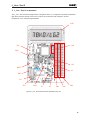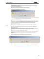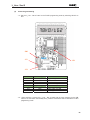
1
To our customers, Old Company Name in Catalogs and Other Documents On April 1st, 2010, NEC Electronics Corporation merged with Renesas Technology Corporation, and Renesas Electronics Corporation took over all the business of both companies. Therefore, although the old company name remains in this document, it is a valid Renesas Electronics document. We appreciate your understanding. Renesas Electronics website: http://www.renesas.com April 1st, 2010 Renesas Electronics Corporation Issued by: Renesas Electronics Corporation (http://www.renesas.com) Send any inquiries to http://www.renesas.com/inquiry. Notice 1. 2. 3. 4. 5. 6. 7. All information included in this document is current as of the date this document is issued. Such information, however, is subject to change without any prior notice. Before purchasing or using any Renesas Electronics products listed herein, please confirm the latest product information with a Renesas Electronics sales office. Also, please pay regular and careful attention to additional and different information to be disclosed by Renesas Electronics such as that disclosed through our website. Renesas Electronics does not assume any liability for infringement of patents, copyrights, or other intellectual property rights of third parties by or arising from the use of Renesas Electronics products or technical information described in this document. No license, express, implied or otherwise, is granted hereby under any patents, copyrights or other intellectual property rights of Renesas Electronics or others. You should not alter, modify, copy, or otherwise misappropriate any Renesas Electronics product, whether in whole or in part. Descriptions of circuits, software and other related information in this document are provided only to illustrate the operation of semiconductor products and application examples. You are fully responsible for the incorporation of these circuits, software, and information in the design of your equipment. Renesas Electronics assumes no responsibility for any losses incurred by you or third parties arising from the use of these circuits, software, or information. When exporting the products or technology described in this document, you should comply with the applicable export control laws and regulations and follow the procedures required by such laws and regulations. You should not use Renesas Electronics products or the technology described in this document for any purpose relating to military applications or use by the military, including but not limited to the development of weapons of mass destruction. Renesas Electronics products and technology may not be used for or incorporated into any products or systems whose manufacture, use, or sale is prohibited under any applicable domestic or foreign laws or regulations. Renesas Electronics has used reasonable care in preparing the information included in this document, but Renesas Electronics does not warrant that such information is error free. Renesas Electronics assumes no liability whatsoever for any damages incurred by you resulting from errors in or omissions from the information included herein. Renesas Electronics products are classified according to the following three quality grades: “Standard”, “High Quality”, and “Specific”. The recommended applications for each Renesas Electronics product depends on the product’s quality grade, as indicated below. You must check the quality grade of each Renesas Electronics product before using it in a particular application. You may not use any Renesas Electronics product for any application categorized as “Specific” without the prior written consent of Renesas Electronics. Further, you may not use any Renesas Electronics product for any application for which it is not intended without the prior written consent of Renesas Electronics. Renesas Electronics shall not be in any way liable for any damages or losses incurred by you or third parties arising from the use of any Renesas Electronics product for an application categorized as “Specific” or for which the product is not intended where you have failed to obtain the prior written consent of Renesas Electronics. The quality grade of each Renesas Electronics product is “Standard” unless otherwise expressly specified in a Renesas Electronics data sheets or data books, etc. “Standard”: 8. 9. 10. 11. 12. Computers; office equipment; communications equipment; test and measurement equipment; audio and visual equipment; home electronic appliances; machine tools; personal electronic equipment; and industrial robots. “High Quality”: Transportation equipment (automobiles, trains, ships, etc.); traffic control systems; anti-disaster systems; anticrime systems; safety equipment; and medical equipment not specifically designed for life support. “Specific”: Aircraft; aerospace equipment; submersible repeaters; nuclear reactor control systems; medical equipment or systems for life support (e.g. artificial life support devices or systems), surgical implantations, or healthcare intervention (e.g. excision, etc.), and any other applications or purposes that pose a direct threat to human life. You should use the Renesas Electronics products described in this document within the range specified by Renesas Electronics, especially with respect to the maximum rating, operating supply voltage range, movement power voltage range, heat radiation characteristics, installation and other product characteristics. Renesas Electronics shall have no liability for malfunctions or damages arising out of the use of Renesas Electronics products beyond such specified ranges. Although Renesas Electronics endeavors to improve the quality and reliability of its products, semiconductor products have specific characteristics such as the occurrence of failure at a certain rate and malfunctions under certain use conditions. Further, Renesas Electronics products are not subject to radiation resistance design. Please be sure to implement safety measures to guard them against the possibility of physical injury, and injury or damage caused by fire in the event of the failure of a Renesas Electronics product, such as safety design for hardware and software including but not limited to redundancy, fire control and malfunction prevention, appropriate treatment for aging degradation or any other appropriate measures. Because the evaluation of microcomputer software alone is very difficult, please evaluate the safety of the final products or system manufactured by you. Please contact a Renesas Electronics sales office for details as to environmental matters such as the environmental compatibility of each Renesas Electronics product. Please use Renesas Electronics products in compliance with all applicable laws and regulations that regulate the inclusion or use of controlled substances, including without limitation, the EU RoHS Directive. Renesas Electronics assumes no liability for damages or losses occurring as a result of your noncompliance with applicable laws and regulations. This document may not be reproduced or duplicated, in any form, in whole or in part, without prior written consent of Renesas Electronics. Please contact a Renesas Electronics sales office if you have any questions regarding the information contained in this document or Renesas Electronics products, or if you have any other inquiries. (Note 1) “Renesas Electronics” as used in this document means Renesas Electronics Corporation and also includes its majorityowned subsidiaries. (Note 2) “Renesas Electronics product(s)” means any product developed or manufactured by or for Renesas Electronics. User’s Manual L_Line - See it! Demonstration Kit for the L_Line Family Global Document No. U18137EE1V0UM00 (1st edition) Document No. L_LINESEEITV100 Date Published September 2005 NEC Electronics (Europe) GmbH L_Line - See it! ・ The information in this document is current as of date of its publication. The information is subject to change without notice. For actual design-in, refer to the latest publications of NEC Electronics data sheets or data books, etc., for the most up-to-date specifications of NEC Electronics products. Not all products and/or types are available in every country. Please check with an NEC sales representative for availability and additional information. ・ No part of this document may be copied or reproduced in any form or by any means without prior written consent of NEC Electronics. NEC Electronics assumes no responsibility for any errors that may appear in this document. ・ NEC Electronics does not assume any liability for infringement of patents, copyrights or other intellectual property rights of third parties by or arising from the use of NEC Electronics products listed in this document or any other liability arising from the use of such NEC Electronics products. No license, express, implied or otherwise, is granted under any patents, copyrights or other intellectual property rights of NEC Electronics or others. ・ Descriptions of circuits, software and other related information in this document are provided for illustrative purposes in semiconductor product operation and application examples. The incorporation of these circuits, software and information in the design of customer's equipment shall be done under the full responsibility of customer. NEC Electronics no responsibility for any losses incurred by customers or third parties arising from the use of these circuits, software and information. ・ While NEC Electronics endeavors to enhance the quality, reliability and safety of NEC Electronics products, customers agree and acknowledge that the possibility of defects thereof cannot be eliminated entirely. To minimize risks of damage to property or injury (including death) to persons arising from defects in NEC Electronics products, customers must incorporate sufficient safety measures in their design, such as redundancy, fire-containment and anti-failure features. ・ NEC Electronics products are classified into the following three quality grades: “Standard”, “Special” and “Specific”. The "Specific" quality grade applies only to NEC Electronics products developed based on a customerdesignated “quality assurance program” for a specific application. The recommended applications of NEC Electronics product depend on its quality grade, as indicated below. Customers must check the quality grade of each NEC Electronics product before using it in a particular application. "Standard": Computers, office equipment, communications equipment, test and measurement equipment, audio and visual equipment, home electronic appliances, machine tools, personal electronic equipment and industrial robots. "Special": Transportation equipment (automobiles, trains, ships, etc.), traffic control systems, antidisaster systems, anti-crime systems, safety equipment and medical equipment (not specifically designed for life support). "Specific": Aircraft, aerospace equipment, submersible repeaters, nuclear reactor control systems, life support systems and medical equipment for life support, etc. The quality grade of NEC Electronics products is “Standard” unless otherwise expressly specified in NEC Electronics data sheets or data books, etc. If customers wish to use NEC Electronics products in applications not intended by NEC Electronics, they must contact NEC Electronics sales representative in advance to determine NEC Electronics 's willingness to support a given application. Notes: 1." NEC Electronics" as used in this statement means NEC Electronics Corporation and also includes its majority-owned subsidiaries. 2. " NEC Electronics products" means any product developed or manufactured by or for NEC Electronics (as defined above). M8E 02.10 2 L_Line - See it! CAUTION This is a Test- and Measurement equipment with possibility to be significantly altered by user through hardware enhancements/modifications and/or test or application software. Thus, with respect to Council Directive 89/336/EEC (Directive on compliance with the EMC protection requirements), this equipment has no autonomous function. Consequently this equipment is not marked by the CE-symbol. EEDT-ST-0005-10 Redemption of Waste Electrical and Electronic Equipment (WEEE) in accordance with legal regulations applicable in the European Union only: This equipment (including all accessories) is not intended for household use. After use the equipment cannot be disposed of as household waste. NEC Electronics (Europe) GmbH offers to take back the equipment. All you need to do is register at www.eu.necel.com/weee. 3 L_Line - See it! Revision History Date 05-09-2005 Revision V1.00 Chapter --- Description First release 4 L_Line - See it! Table of Contents 1. Introduction ....................................................................................................................... 9 1.1 1.2 1.3 1.4 Main features of L_Line – See it! ................................................................................................. 9 System requirements ................................................................................................................. 10 Package contents....................................................................................................................... 10 Trademarks................................................................................................................................. 10 2. L_Line - See it! system configuration ............................................................................ 11 2.1 2.2 2.3 L_Line - See it!............................................................................................................................ 11 Host computer............................................................................................................................ 11 Power supply via USB interface ................................................................................................ 11 3. L_Line - See it! components........................................................................................... 12 3.1 3.2 3.3 3.4 3.4.1 3.4.2 3.4.3 3.4.4 3.5 3.6 3.7 3.8 3.9 3.9.1 3.10 3.11 3.12 3.13 3.14 3.15 3.16 Power supply selection, Jumper JP1........................................................................................ 14 OCD power supply, Jumper JP2 ............................................................................................... 14 Clock supply, Jumper JP3 ......................................................................................................... 14 Configuration switch SW1 ......................................................................................................... 15 Operation mode selection, SW1/S1........................................................................................... 15 UART selection, SW1/S2 .......................................................................................................... 15 On-Chip debug enable, SW1/S3................................................................................................ 15 On-Chip debug mode select, SW1/S4 ....................................................................................... 16 RESET button, SW2 ................................................................................................................... 16 Navigation switch, SW3 ............................................................................................................. 16 Soldering bridges SB1, SB3, SB4, SB5 and SB6...................................................................... 17 USB interface connector CN7 .................................................................................................... 18 FLASH programmer connector CN2.......................................................................................... 19 OCD connector CN8.................................................................................................................. 20 LCD1, 112 segment standard LCD panel ................................................................................ 21 Temperature sensor ................................................................................................................. 22 Phototransistor, Q1 .................................................................................................................. 26 Buzzer, BUZ1 ............................................................................................................................ 26 Battery holder, BAT1 ................................................................................................................ 26 External connector CN3, CN4 and CN5 ................................................................................... 27 78K0/LG2 memory map ............................................................................................................ 28 4. On-Chip debugging ......................................................................................................... 29 4.1 4.2 OCD via On-Board debug function ........................................................................................... 29 OCD via QB-78K0MINI emulator ................................................................................................ 30 5. L_Line - See it! installation and operation..................................................................... 31 5.1 Getting started............................................................................................................................ 31 5.1.1 CD-ROM contents ..................................................................................................................... 31 6. Hardware installation ...................................................................................................... 32 7. Software installation........................................................................................................ 32 5 L_Line - See it! 7.1 7.2 7.3 7.4 7.5 7.5.1 7.5.2 7.5.3 7.6 7.7 8. IAR Systems Embedded Workbench for 78K0/78K0S installation .......................................... 32 Device file installation................................................................................................................ 32 FPL3 FLASH programming GUI installation ............................................................................. 32 Sample program installation ..................................................................................................... 32 USB Driver Installation............................................................................................................... 33 Installation on Windows 98SE/Me.............................................................................................. 33 Installation on Windows 2000 .................................................................................................... 35 Installation on Windows XP ....................................................................................................... 41 Confirmation of USB Driver Installation ................................................................................... 46 Driver deinstallation ................................................................................................................... 47 FPL3 FLASH programming software.............................................................................. 49 8.1 8.2 8.3 8.4 8.4.1 8.4.2 8.4.3 8.4.4 8.5 Introduction ................................................................................................................................ 49 Starting up the GUI Software..................................................................................................... 49 Toolbar........................................................................................................................................ 50 Menu Bar..................................................................................................................................... 51 [File] menu ................................................................................................................................ 51 [Device] menu ........................................................................................................................... 52 [View] menu .............................................................................................................................. 61 [Help] menu............................................................................................................................... 62 Programmer Parameter Window ............................................................................................... 63 9. How to use FPL3 FLASH programming software .......................................................... 64 (1) (2) (3) (4) (5) (6) (7) (8) (9) (10) Installing the FPL3 GUI software................................................................................................... 64 Installing the driver........................................................................................................................ 64 Installing the parameter file ........................................................................................................... 64 Connecting and starting ................................................................................................................ 65 Setting the programming environment .......................................................................................... 66 Selecting a user program .............................................................................................................. 69 [Autoprocedure(EPV)] command execution................................................................................... 70 Terminating the GUI ..................................................................................................................... 70 Execute “78K0_LCD_DEMO” application ...................................................................................... 70 Restarting the GUI ...................................................................................................................... 70 10. TROUBLESHOOTING .................................................................................................... 71 11. IAR configuration for On-Board debugging................................................................. 73 11.1 11.2 Setup COM port for IAR C-SPY debugger............................................................................... 73 Configuration of USB serial COM port.................................................................................... 73 12. IAR sample session ....................................................................................................... 76 13. Sample Project .............................................................................................................. 81 13.1 13.2 13.3 13.4 13.5 Real-Time-Clock function ........................................................................................................ 82 Temperature measurement ...................................................................................................... 82 Light incidence measurement ................................................................................................. 82 BUZZER output example.......................................................................................................... 82 Menu control............................................................................................................................. 83 6 L_Line - See it! 14. Cables ............................................................................................................................ 84 14.1 USB interface cable (Mini-B type)............................................................................................ 84 15. Schematics .................................................................................................................... 85 List of Figures Figure 1: L_Line - See it! system configuration ...................................................................................... 11 Figure 2: L_Line - See it! board connectors and switches, top view........................................................ 12 Figure 3: L_Line - See it! board connectors and switches, button view................................................... 13 Figure 4: Soldering bridges SB1, SB3-SB6............................................................................................ 17 Figure 5: Connector CN7, USB Mini-B Type Host Connector Pin Configuration..................................... 18 Figure 6: LCD panel / segment definition............................................................................................... 21 Figure 7: Typical dependence of sensor resistance................................................................................ 22 Figure 8: Diagram of dual slope circuit .................................................................................................. 25 Figure 9: 78K0/LG2 memory map ......................................................................................................... 28 Figure 10: Add New Hardware Wizard (Windows 98SE)....................................................................... 33 Figure 11: Search Method (Windows 98SE) .......................................................................................... 33 Figure 12: Search Location Specification (Windows 98SE).................................................................... 34 Figure 13: Checking Driver to Be Installed (Windows 98SE).................................................................. 34 Figure 14: Installation Completion (Windows 98SE) .............................................................................. 35 Figure 15: Found New Hardware Wizard 1 (Windows 2000) .................................................................. 35 Figure 16: Search Method 1 (Windows 2000) ........................................................................................ 36 Figure 17: Driver File Location 1 (Windows 2000) ................................................................................. 36 Figure 18: Address Specification 1 (Windows 2000) .............................................................................. 37 Figure 19: Driver File Search 1 (Windows 2000) ................................................................................... 37 Figure 20: USB Driver Installation Completion 1 (Windows 2000).......................................................... 38 Figure 21: Found New Hardware Wizard 2 (Windows 2000) .................................................................. 38 Figure 22: Search Method 2 (Windows 2000) ........................................................................................ 39 Figure 23: Driver File Location 2 (Windows 2000) ................................................................................. 39 Figure 24: Address Specification 2 (Windows 2000) .............................................................................. 40 Figure 25: Driver File Search 2 (Windows 2000) ................................................................................... 40 Figure 26: USB Driver Installation Completion 2 (Windows 2000).......................................................... 41 Figure 27: Found New Hardware Wizard 1 (Windows XP) ..................................................................... 41 Figure 28: Search Location Specification 3 (Windows XP)..................................................................... 42 Figure 29: Windows XP Logo Testing 3 (Windows XP) .......................................................................... 42 Figure 30: USB Driver Installation Completion 1 (Windows XP)............................................................. 43 Figure 31: Found New Hardware Wizard 2 (Windows XP) ..................................................................... 43 Figure 32: Search Location Specification 2 (Windows XP)..................................................................... 44 Figure 33: Windows XP Logo Testing 2 (Windows XP) .......................................................................... 44 Figure 34: USB Serial Port2 Driver Installation Completion (Windows XP) ............................................ 45 Figure 35: Device Manager ................................................................................................................... 46 Figure 36: Driver Uninstallation ............................................................................................................. 47 Figure 37: Driver Uninstaller.................................................................................................................. 47 Figure 38: Completion of Driver Uninstallation....................................................................................... 48 Figure 39: GUI Software Main Window.................................................................................................. 49 Figure 40: Toolbar Buttons .................................................................................................................... 50 Figure 41: [File] Menu ........................................................................................................................... 51 Figure 42: HEX File Selection Window .................................................................................................. 51 Figure 43: [Device] Menu ...................................................................................................................... 52 Figure 44: Device Setup Window - Standard ......................................................................................... 54 Figure 45: Device Setup Window - Parameter File Selection................................................................. 55 Figure 46: Parameter File Selection Window......................................................................................... 55 Figure 47: Device Setup Window – Host connection.............................................................................. 56 Figure 48: Device Setup Window - Supply Oscillator Selection ............................................................. 56 Figure 49: Device Setup Window - Operation Mode .............................................................................. 57 Figure 50: Device Setup Window – Target Reset Message ................................................................... 57 7 L_Line - See it! Figure 51: Device Setup Window - Advance.......................................................................................... 58 Figure 52: Device Setup Window - Command options........................................................................... 58 Figure 53: Device Setup Window – Security flag settings ...................................................................... 59 Figure 54: Device Setup Window – Disable Chip Erase......................................................................... 60 Figure 55: Device Setup Window – Disable Boot Cluster Reprogramming warning................................ 60 Figure 56: [View] Menu.......................................................................................................................... 61 Figure 57: [Help] Menu .......................................................................................................................... 62 Figure 58: About FPL3 Window............................................................................................................. 62 Figure 59: Programmer Parameter Window .......................................................................................... 63 Figure 60: GUI Software Startup Screen................................................................................................ 66 Figure 61: <Standard Device Setup> Dialog Box................................................................................... 66 Figure 62: Parameter File Selection ...................................................................................................... 67 Figure 63: Port Selection ....................................................................................................................... 67 Figure 64: <Standard Device Setup> Dialog Box after Setting............................................................... 68 Figure 65: <Advance Device Setup> Dialog Box ................................................................................... 68 Figure 66: Completion of Parameter Setting.......................................................................................... 69 Figure 67: After Downloading ................................................................................................................ 69 Figure 68: After EPV Execution............................................................................................................. 70 Figure 69: Registry entry for IAR C-SPY debugger COM port setting..................................................... 73 Figure 70: Configuration of COM port for IAR C-SPY debugger 1/4....................................................... 73 Figure 71: Configuration of COM port for IAR C-SPY debugger 2/4....................................................... 74 Figure 72: Configuration of COM port for IAR C-SPY debugger 3/4....................................................... 74 Figure 73: Configuration of COM port for IAR C-SPY debugger 4/4....................................................... 75 Figure 74: IAR Embedded Workbench .................................................................................................. 76 Figure 75: IAR project workspace .......................................................................................................... 77 Figure 76: IAR debugger options ........................................................................................................... 77 Figure 77: IAR Linker options ................................................................................................................ 78 Figure 78: TK-78 hardware setup menu................................................................................................. 78 Figure 79: IAR project download............................................................................................................ 79 Figure 80: IAR C-SPY debugger............................................................................................................ 80 Figure 81: Menu control......................................................................................................................... 83 Figure 82: USB interface cable (Mini-B type)......................................................................................... 84 Figure 83: L_Line - See it! schematics 1/3 ............................................................................................. 85 Figure 84: L_Line - See it! schematics 2/3 ............................................................................................. 86 Figure 85: L_Line - See it! schematics 3/3 ............................................................................................. 87 List of Tables Table 1: Power supply selection, Jumper JP1........................................................................................ 14 Table 2: OCD power supply, Jumper JP2 .............................................................................................. 14 Table 3: Clock supply, Jumper JP3 ....................................................................................................... 14 Table 4: Configuration switch SW1, factory settings .............................................................................. 15 Table 5: Operation mode selection SW1/S1 .......................................................................................... 15 Table 6: UART selection SW1/S2.......................................................................................................... 15 Table 7: On-Chip debug enable SW1/S3............................................................................................... 15 Table 8: On-Chip debug mode select SW1/S4 ...................................................................................... 16 Table 9: Navigation switch SW3 ............................................................................................................ 16 Table 10: Setting of soldering bridges SB1, SB3-SB6............................................................................ 17 Table 11: Pin Configuration of USB Connector CN7 .............................................................................. 18 Table 12: CN4, PG-FP4 connector ........................................................................................................ 19 Table 13: Hardware configuration when using PG-FP4.......................................................................... 19 Table 14: OCD connector CN8 .............................................................................................................. 20 Table 15: SW1 configuration for OCD ................................................................................................... 20 Table 16: LCD pin assignments / connections ....................................................................................... 21 Table 17: Distribution of temperature factor kT ....................................................................................... 22 Table 18: CN3, CN4, and CN5 connection to 78K0/LG2 ........................................................................ 27 Table 19: L_Line - See it! CD-ROM directory structure .......................................................................... 31 Table 20: Sample project directory structure.......................................................................................... 81 8 L_Line - See it! 1. Introduction L_Line - See it! is a demonstration kit for the NEC’s L_Line 8-Bit microcontroller family with integrated LCD controller. It supports onboard FLASH programming and real time execution of application programs up to 4 kBytes of program code. The board is prepared to be connected to user hardware parts such as digital I/O or analogue signals. 1.1 Main features of L_Line – See it! • Easy to use device demonstration capabilities L_Line - See it! contains elements to easily demonstrate simple I/O-functions, i.e. navigator switch, 112 segment LCD panel, phototransistor, temperature sensor, I/O lines, UART serial interface etc. • On-Board debug function The K_Line – Lin it! supports an On-Board debug function by using the IAR C-SPY debugger. It Allows FLASH downloading and standard debug functions i.e. code execution, single stepping, breakpoints, memory manipulation etc. • Flexible power supply The K_Line – Lin it! supports a flexible configuration of it’s power supply. The board can be powered by the USB interface, the QB-78K0MINI On-Chip debug emulator as well by an external CR2032 3V lithium coin battery. • LCD panel L_Line - See it! provides a 112 segment standard LCD panel, allowing the implementation of human / machine interface, comfortable input / output functions, output of measurement values, output of status information etc. • FPL3, FLASH programming software A windows based FLASH programming software allows to select and download application programs to the L_Line - See it! board for evaluation purposes. • Analogue to digital signal conversion is supported • Various input / output signals available, such as ° ° ° ° ° ° ° ° ° • All I/O ports prepared to be connected to user hardware 112 segment standard LCD panel, 8 digits a 14 segments each Timer input / output signals Two or three wire serial I/O UART interface, via USB UART chip FT232 8 analogue input lines Temperature sensor KTY13-5 Phototransistor PT15-21C Navigation switch prepared for key interrupt generation The IAR Embedded Workbench for 78K0/78K0S and the IAR C-SPY debugger / simulator are included. These packages are restricted in such that maximum program code size is limited to 4 kByte of program code. • Full documentation is included for the NEC 78K0/LG2 microcontroller, IAR Systems Embedded Workbench, IAR Systems C-SPY debugger / simulator and the NEC FPL3 FLASH programming software. L_Line - See it! is not intended for code development. NEC does not allow and does not support in any way any attempt to use L_Line - See it! in a commercial or technical product. 9 L_Line - See it! 1.2 System requirements HOST PC A PC supporting Windows 98SE, Windows ME, Windows 2000 or Windows XP is required for the IAR Systems Embedded Workbench demo-version and the FPL3 FLASH programming software. Pentium 166 MHz (at least), 128 MB of RAM, 256-color display (1024 * 768), mouse, CD-ROM drive and 200 Mbytes of free hard disk space are required to install the tool packages. Above listed requirements are valid for the IAR Systems Embedded Workbench and the FPL3 FLASH programming software. Host interface USB interface that enables communication based on USB (Ver1.1 or later) 1.3 Package contents Please verify that you have received all parts listed in the package contents list attached to the L_Line - See it! package. If any part is missing or seems to be damaged, please contact the dealer from whom you received your L_Line - See it!. Note: Updates of the IAR Embedded Workbench for 78K, FP3 FLASH programming software, documentation and/or utilities for L_Line - See it!, if available, may be downloaded from the NEC WEB page(s) at http://www.eu.necel.com/updates 1.4 Trademarks IAR Embedded Workbench, visualSTATE, IAR MakeApp and C-SPY are registered trademarks of IAR Systems AB. Microsoft and Windows are registered trademarks of Microsoft Corporation. Adobe and Acrobat Reader are registered trademarks of Adobe Systems Incorporated. All other product names are trademarks or registered trademarks of their respective owners. 10 L_Line - See it! 2. L_Line - See it! system configuration The L_Line - See it! system configuration is given in the diagram below: Figure 1: L_Line - See it! system configuration 2.1 L_Line - See it! L_Line – See it! is a demonstration kit for the 78K0/LG2 8-Bit microcontroller with integrated LCD controller. The L_Line – See it! board is connected to the host system via USB interface cable. The host system may be used for onboard FLASH programming of the 78K0/LG2 internal FLASH memory and to allow execution of application programs on L_Line – See it! starterkit. Additionally it supports On-Chip debug functionality by using the IAR C-SPY debugger. L_Line - See it! runs the microcontroller at 6.0000 MHz operating speed. Sub-clock is provided with 32.768 kHz. 2.2 Host computer The USB host interface enables communication to the L_Line - See it! board. The USB UART chip FT232 allows application software to access the USB device in the same way as it would access a standard RS232 interface. The FTDI's Virtual COM Port ( VCP ) driver appears to the windows system as an extra Com Port, in addition to any existing hardware Com Ports. 2.3 Power supply via USB interface The L_Line - See it! supports a flexible configuration of it’s power supply. The board can be powered by the USB interface, the QB-78K0MINI On-Chip debug emulator as well by an external CR2032 3V lithium coin battery (not assembled). 11 L_Line - See it! 3. L_Line - See it! components The L_Line - See it! board is equipped with a navigation switch, a 112 segment LCD panel, temperature / light sensor and with several connectors in order to be connected to host computers, FLASH programmer or any external target hardware. LCD1 CN7 CN8 SW2 JP3 BUZ1 X1 SW1 JP1 JP2 SW3 S1 Q1 CN3 CN4 CN5 Figure 2: L_Line - See it! board connectors and switches, top view 12 L_Line - See it! CN2 BAT1 Figure 3: L_Line - See it! board connectors and switches, button view Some of the L_Line – See it! components are free for user application hardware and software. Please read the user’s manual of the 78K0/LG2 device carefully to get information about the electrical specification of the available I/O ports before you connect any external signals to the L_Line – See it! board. 13 L_Line - See it! 3.1 Power supply selection, Jumper JP1 The different power supply modes of the L_Line - See it! board can be set by jumper JP1. Jumper JP1 controls the power supply during the stand-alone, FLASH programming and On-Board debugging mode. Additionally power supply can be applied by the QB-78K0MINI On-Chip debug emulator, controller by jumper JP2. JP1 1-2 Jumper Setting Closed (default) 2-3 Closed Mode Power supply via USB interface, CN7 Power supply via battery, BAT1 Table 1: Power supply selection, Jumper JP1 3.2 OCD power supply, Jumper JP2 The power supply of the L_Line - See it! board can also be applied by the QB-78K0MINI On-Chip debug emulator. Close jumper JP2 to apply power from the QB-78K0MINI. JP2 1-2 Jumper Setting Open (default) Mode Power supply via USB or Battery Power supply via QB-78K0MINI emulator Closed Table 2: OCD power supply, Jumper JP2 3.3 Clock supply, Jumper JP3 The clock supply of the 78K0/LG2 device is controlled by jumper JP3. By closing JP3 external frequency of 6 MHz is applied to the P122/X2 clock input pin of the 78K0/LG2 device. When opening JP3 an external oscillator can be used. To use this mode equip pad X1 (not assembled) of the L_Line – See it! board with an corresponding oscillator. JP3 1-2 Jumper Setting Closed (default) Open Mode Clock frequency = 6 MHz, supplied by CPLD • Clock supply by external oscillator. By using this mode be sure to equip a crystal oscillator to the X1 pad. • For using the QB-78K0MINI On-Chip debug emulator Table 3: Clock supply, Jumper JP3 14 L_Line - See it! 3.4 Configuration switch SW1 The different operation modes of the L_Line - See it! board can be set by SW1 switches S1-S4. SW1 S1 S2 S3 S4 Factory settings OFF OFF OFF OFF Mode Normal operation mode UART6 select OCD disabled On-Board debug function Table 4: Configuration switch SW1, factory settings 3.4.1 Operation mode selection, SW1/S1 SW1 switch S1 controls the operation mode of the L_Line - See it! board. Setting SW1/S1 to ON allows to reprogram the internal FLASH memory of the 78K0/LG2 device by using the FPL3 FLASH programming software. SW1, S1 OFF (default) ON Mode Normal operation mode FLASH memory programming mode Table 5: Operation mode selection SW1/S1 Within the normal operation mode the user program stored in the FLASH memory of 78K0/LG2 is executed. 3.4.2 UART selection, SW1/S2 SW1 switch S2 specifies the corresponding UART signals of the 78K0/LG2 device that are connected to the FT232 interface lines. SW1, S2 OFF (default) ON Mode UART6 select UART0 select Table 6: UART selection SW1/S2 3.4.3 On-Chip debug enable, SW1/S3 SW1 switch S3 controls the On-Chip debugging for the 78K0/LG2 device. Setting switch S3 to ON allows to use the On-Board debug function of the L_Line – See it! board and additionally the connection of the QB-78K0MINI On-Chip debug emulator. SW1, S3 OFF (default) ON On-Chip debug Disabled Enabled Table 7: On-Chip debug enable SW1/S3 15 L_Line - See it! 3.4.4 On-Chip debug mode select, SW1/S4 SW1 switch S4 controls the On-Chip debug mode of L_Line - See it! board. Switching SW1/S4 to OFF allows to use the On-Board debug function of L_Line – See it! board. By using this mode no additional debug hardware like the QB78K0MINI On-Chip debug emulator is needed. The debugging is done via the default USB/UART connection to the Host computer. All standard debug function are available in the On-Board debug mode like FLASH programming / downloading, code execution, single stepping, breakpoints, memory manipulation etc. Setting switch SW1/S4 to ON allows connecting the QB-78K0MINI On-Chip debug emulator to the L_Line – See it! board in order to use On-Chip debug function of the 78K0/LG2 device. The QB78K0MINI is a separate product from NEC and it is not included in this starterkit package SW1, S4 OFF (default) ON OCD mode On-Board debug function QB-78K0MINI Table 8: On-Chip debug mode select SW1/S4 3.5 RESET button, SW2 SW2 is the reset button. It activates the power on reset. It is connected to the reset input of the 78K0/LG2 microcontroller. Note: By supplying power to the L_Line – See it! board via the battery the RESET button becomes inactive. Please use jumper JP1 to power OFF/ON the microcontroller. 3.6 Navigation switch, SW3 Button SW3 is a navigation switch connected to the key interrupt port of the 78K0/LG2 device. It operates in five directions including a center push function. The connection of SW3 is shown in the table below: Up (KR0) Right (KR2) Left (KR3) Select (KR4) SW3 Connection to the 78K0/LG2 device Left Down Select Right Up P73/KR3 P71/KR1 P74/KR4 P72/KR2 P70/KR0 Down (KR1) Table 9: Navigation switch SW3 16 L_Line - See it! 3.7 Soldering bridges SB1, SB3, SB4, SB5 and SB6 Additional configuration of the L_Line – See it! board can be done by the soldering bridges SB1, SB3, SB4, SB5 and SB6. The different configuration modes are shown in the table below: SB1 3 2 1 SB3 SB4 SB5 111 SB6 111 3 2 1 1 2 3 111 111 1 2 3 Figure 4: Soldering bridges SB1, SB3-SB6 Soldering bridge SB1 Pad Configuration Mode 1-2 SB3 1-2 2-3 1-2 2-3 1-2 2-3 1-2 2-3 1-2 2-3 1-2 2-3 1-2 2-3 1-2 2-3 Closed (default) Open Closed (default) Open (default) Open Closed Closed (default) Open (default) Open Closed Closed (default) Open (default) Open Closed Closed (default) Open (default) Open Closed VCC connected to AVREF pin VCC disconnected from AVREF pin Sub Clock Oscillator connected to P123/XT1 pin SB4 SB5 SB6 P123/XT1 pin connected to CN5-2 Sub Clock Oscillator connected to P124/XT2 pin P124/XT2 pin connected to CN5-4 Main Clock Oscillator connected to P121/X1 pin P121/X1 pin connected to CN3-38 Main Clock Oscillator connected to P121/X2 pin P121/X2 pin connected to CN3-40 Table 10: Setting of soldering bridges SB1, SB3-SB6 By cutting the default connections (pad 1-2) of soldering bridges SB3/SB4 respectively SB5/SB6 and closing pads 2-3, the corresponding microcontroller signals are connected to the external connectors CN3 respectively CN5. In this mode the microcontroller pins can be used as standard I/O ports. Please configure the clock generator of the 78K0/LG2 device accordingly to use this mode. Note: Do not close the connection for the Clock Oscillator and external connectors at the same time. This can affect the operation of the Sub / Main clock oscillator negatively. 17 L_Line - See it! 3.8 USB interface connector CN7 The CN7 connector allows connecting the FPL3 FLASH programming software to the L_Line - See it! board in order to program application software into the CPU internal flash. Additionally the On-Board debug function uses connector CN7 for communication with the host computer. The board power supply of 5V is also provided by connector CN7. For standard communication to a host system i.e. by using a terminal program the input/output signals of UART6 respectively UART0 of the 78K0/LG2 device are connected to CN7. 1 5 Figure 5: Connector CN7, USB Mini-B Type Host Connector Pin Configuration USB Connector CN7 1 2 3 4 5 Signal Name VBUS DM DP N.C. GNDBUS Table 11: Pin Configuration of USB Connector CN7 For connection with the host machine, use a USB cable (Mini-B type). For confirmation, NEC Electronics used only the USB cable delivered with the L_Line - See it! board. 18 L_Line - See it! 3.9 FLASH programmer connector CN2 Connector CN2 (not assembled) allows connecting the PG-FP4 FLASH programmer to L_Line – See it! board in order to program application software into the CPU internal flash memory. Please note, the PG-FP4 FLASH programmer is a separate product from NEC and it is not included in this package. CN2 1 2 3 4 5 6 7 8 9 10 11 12 13 14 15 16 Signal GND RESET SI VCC SO N.C. SCK N.C. N.C. N.C. N.C. FLMD1 N.C. FLMD0 N.C. N.C. Table 12: CN4, PG-FP4 connector When using PG-FP4, the programming interface to the 78K0/LG2 device must be set to the clock serial interface, CSI-Ring-Osc. Please configure the L_Line – See it! board as following: SW1 S1 S2 S3 S4 Jumper JP1 JP2 JP3 Setting OFF OFF OFF OFF Setting 1-2 Closed Open Closed Mode Normal operation mode UART6 select OCD disabled On-Board debug function Mode Power supply via USB Power supply via USB Clock supplied via CPLD Table 13: Hardware configuration when using PG-FP4 19 L_Line - See it! 3.9.1 OCD connector CN8 Connector CN8 (not assembled) allows connecting the QB-78K0MINI On-Chip debug emulator to the L_Line – See it! board in order to use On-Chip debug function of the 78K0/LG2 device. QB-78K0MINI is a separate product from NEC and it is not included in this starterkit package. CN8 1 2 3 4 5 6 7 8 9 10 Signal RESET_IN RESET_OUT FLMD0 VDD_IN X2 GND X1 GND N.C. N.C. Table 14: OCD connector CN8 To enable On-Chip debugging by using the QB-78K0MINI On-Chip debug emulator configure the L_Line – See it! board as following: SW1 S1 S2 S3 S4 Jumper JP1 JP2 JP3 Setting OFF OFF ON ON Setting 1-2 Closed Open Closed Open Mode Normal operation mode UART6 select OCD enabled QB-78K0MINI enabled Mode Power supply via USB Power supply via USB Power supply via QB-78K0MINI (*Note) Clock supplied via QB-78K0MINI Table 15: SW1 configuration for OCD For more details on how to configure L_Line – See it! in order to use On-Chip debugging please refer to CHAPTER 4, ON-CHIP DEBUGGING. 20 L_Line - See it! 3.10 LCD1, 112 segment standard LCD panel The L_Line - See it! board is equipped with a 112 segment standard LCD panel. The LCD is a transflective model type operating at 5V supply voltage. It can operate at a four times multiplex rate. The display can be used within a temperature range of -20°C … +70°C. The typical driving frequency is equal to 32 Hz (max. 100 Hz) within the complete temperature range. The LCD pin assignments, connections and segment definition is shown in table / figure below: LCD panel 78K0/LG2 device Pin COM1 COM2 COM3 COM4 1 2 3 4 5 6 7 8 9 10 11 12 13 14 15 16 17 18 S1 1I S2 2I S3 3I S4 4I S5 5I S6 6I S7 7I S8 8I NC NC 1F 1J 2F 2J 3F 3J 4F 4J 5F 5J 6F 6J 7F 7J 8F 8J NC NC 1E 1K 2E 2K 3E 3K 4E 4K 5E 5K 6E 6K 7E 7K 8E 8K NC COM3 1D 1N 2D 2N 3D 3N 4D 4N 5D 5N 6D 6N 7D 7N 8D 8N COM4 NC S0 S1 S4 S5 S8 S9 S12 S13 S16 S17 S20 S21 S24 S25 S28 S29 COM4 COM3 LCD panel 78K0/LG2 device Pin COM1 COM2 COM3 COM4 36 35 34 33 32 31 30 29 28 27 26 25 24 23 22 21 20 19 1H 1A 2H 2A 3H 3A 4H 4A 5H 5A 6H 6A 7H 7A 8H 8A COM0 NC 1G 1B 2G 2B 3G 3B 4G 4B 5G 5B 6G 6B 7G 7B 8G 8B NC COM1 1L 1C 2L 2C 3L 3C 4L 4C 5L 5C 6L 6C 7L 7C 8L 8C NC NC 1M P1 2M P2 3M P3 4M P4 5M P5 6M P6 7M P7 8M P8 NC NC S2 S3 S6 S7 S10 S11 S14 S15 S18 S19 S22 S23 S26 S27 S30 S31 COM0 COM1 Table 16: LCD pin assignments / connections Figure 6: LCD panel / segment definition 21 L_Line - See it! 3.11 Temperature sensor For temperature measurement and primarily as an application example a silicon temperature sensor KTY13-5 is connected to the input port of the 16-Bit Timer/Event Counter 00, equal to port P00 of 78K0/LG2 device. The temperature sensor has a resistor range of R25 min = 1950 Ω and R25 max = 1990 Ω at 25 degrees centigrade, with IOP = 1mA. The distribution of the temperature factor kT is shown in the table below: 1) Normalising point Table 17: Distribution of temperature factor kT The sensor resistance can be calculated as following: RT = kT * R25 = ∫(TA) Figure 7: Typical dependence of sensor resistance 22 L_Line - See it! The temperature at the sensor can be calculated from the change in the sensors resistance from the following equation, which approximates the characteristic curve: α² - 4 x β + 4 x β x kT T = 25 + with: °C 2xβ -3 α = 7,88 x 10 x K -5 -1 β = 1,937 x 10 x K kT = - α -2 RT R25 The temperature measurement is done by using the dual slope method. Using the dual slope method a resistor value can be converted into a digital counter value. To do this, the charging time of capacitor C18 will be measured with the 16-Bit Timer/Event Counter 00 of the microcontroller. The first charging slope will use a reference resistor (RREF = R6) and the second charging slope will use variable resistor (RVAR= R5 + RT) which should be determined. By the comparison of the two measured times and the known reference resistor RREF the variable resistor can be calculated. The 78K0/LX2 device family has the advantage of bit settable I/O ports and Schmitt-trigger inputs (e.g. timer input port TI000). The L_Line – See it! board uses the bit settable port P0 as a bidirectional port. At first, the complete port P0 is cleared and set to output mode. In this case the capacitor C18 is discharged via P00/TI000 and prepared for the first measurement. The resistor R7 is only used to limit the current during the discharging of the capacitor. Then port P02 is set to 1 and output. At this point also the 16-bit Timer/Event Counter 00 is started. The rest of the port P0 is set to input (high impedance). So the capacitor will be charged via the reference resistor R6. When the capacitor has reached the threshold level of the Schmitt-trigger input P00/TI000, the actual timer value is automatically captured and an internal interrupt is generated. Using this interrupt the capture value is read out. In the next step the capacitor C18 will be discharged again. The same procedure starts once more with port P03. This time the capacitor is charged via the unknown resistor RVAR of the temperature sensor and after the threshold is reached again the second timer value is read out. The unknown RVAR can be calculated from the two values obtained using the method described above and consequently the resistor value of the temperature sensor. Please refer to derivation on the following sides. 23 L_Line - See it! tREF RREF x C RREF: R6 = VCREF = VDD 1 - e tVAR RVAR x C RVAR: R5 + RT = VCREF = VDD 1 - e VC = VCVAR = VCREF = const The threshold level of the Schmitt-trigger input does not have any influence on the accuracy of the measurement. As this will be a constant for both measurements. VDD tREF RREF x C 1- e = - tREF RREF x C 1- e = 1- e - VDD tVAR RVAR x C 1- e tREF RREF x C - tVAR RVAR x C = e tREF RREF x C = tVAR RVAR x C tREF RREF = tVAR RVAR RVAR = RREF x e tVAR RVAR x C tVAR tREF The capacitor C18 and the supply voltage VDD do not have any influence on the accuracy of the measurement. Only the absolute value of the reference resistor RREF has an influence, because these parameters will not change during one measurement. Using the RREF, tREF and tVAR values, the resistor RVAR can be calculated. 24 L_Line - See it! The diagram of the dual slope circuit is shown in the figure below: P02 P03 S1 (RT) 78K0/LG2 R6 R5 P00 / TI000 R7 C18 RREF = R6 RVAR = R5 + RT RT = temperature sensor resistance Figure 8: Diagram of dual slope circuit The calculation of the charging time of the capacitor can be done as following: t RxC VC = VDD 1 - e t VC RxC =1- e VDD t RxC VC = e 1VDD - t RxC = ln 1- VC VDD t = - R x C x ln 1- VC VDD 25 L_Line - See it! Example: VDD = 5 V; Vthreshold = VC = (0,4 … 0,7) VDD Typical: Vthreshold = 0,6 x VDD RREF = 10 kΩ; C = C18 = 220 nF t = - RREF x C x ln 1- t = - 10 kΩ x 220 nF x ln VC VDD 1 - 0,6 t = 2,0158 ms 3.12 Phototransistor, Q1 For light incidence measurement and primarily as an application example a phototransistor PT15-21C is connected to the ANI0 analogue input, equal to port P20 of the 78K0/LG2 device. 3.13 Buzzer, BUZ1 To generate acoustic signals and sound waves a buzzer is connected to the timer output port of the 16Bit Timer/Event Counter 01, equal to port P06/TI011/TO01 of the 78K0/LG2 device. The AC buzzer operates in a voltage range of 2V…5V. 3.14 Battery holder, BAT1 To power the L_Line – See it! board via battery, please equip the battery holder BAT1 with a CR2032 3V lithium coin type battery. 26 L_Line - See it! 3.15 External connector CN3, CN4 and CN5 CN3, CN4 and CN5 are connectors for external user hardware. The microcontroller signals are connected to CN3, CN4 and CN5. The L_Line - See it! board provides also a wire wrap field area connector CN3 - allowing the integration of additional application hardware. CN3 Signal CN3 1 VCC 2 3 VCC 4 5 VCC 6 7 VCC 8 9 VCC 10 11 VCC 12 13 VCC 14 15 VCC 16 17 VCC 18 19 VCC 20 21 VCC 22 23 VCC 24 25 VCC 26 27 VCC 28 29 VCC 30 31 VCC 32 33 VCC 34 35 VCC 36 37 VCC 38 39 VCC 40 (N.C. = Not Connected) Signal CN4 Signal CN4 Signal CN5 Signal CN5 Signal P25/ANI5 P26/ANI6 P27/ANI7 P30/INTP1 P31/INTP2 P32/INTP3 P33/INTP4/TI51/TO51 P60/SCL0 P61/SDA0 P70/KR0 P71/KR1 P72/KR2 P73/KR3 P74/KR4 P75/KR5 P76/KR6 P77/KR7 P120/INTP0/EXLVI P121/X1 P122/X2 1 3 5 7 9 11 13 15 17 19 21 23 25 27 29 31 33 35 37 39 2 4 6 8 10 12 14 16 18 20 22 24 26 28 30 32 34 36 38 40 P00/TI000 P01/TI010/TO00 P02/SO11 P03/SI11 P04/SCK11 P05/TI001/SSI11 P06/TI011/TO01 P10/SCK10/TXD0 P11/SI10/RXD0 P12/SO10 P13/TXD6 P14/RXD6 P15/TOH0 P16/TOH1/INTP5 P17/TI50/TO50 P20/ANI0 P21/ANI1 P22/ANI2 P23/ANI3 P24/ANI4 1 3 5 7 9 11 13 15 17 19 21 23 25 27 29 31 33 35 37 39 N.C. N.C. N.C. N.C. N.C. N.C. N.C. N.C. N.C. N.C. N.C. N.C. N.C. N.C. N.C. N.C. N.C. N.C. N.C. N.C. P123/XT1 P124/XT2 N.C. N.C. N.C. N.C. N.C. N.C. N.C. N.C. N.C. N.C. N.C. N.C. N.C. N.C. N.C. N.C. N.C. N.C. VSS VSS VSS VSS VSS VSS VSS VSS VSS VSS VSS VSS VSS VSS VSS VSS VSS VSS VSS VSS 2 4 6 8 10 12 14 16 18 20 22 24 26 28 30 32 34 36 38 40 Table 18: CN3, CN4, and CN5 connection to 78K0/LG2 27 L_Line - See it! 3.16 78K0/LG2 memory map The memory layout of 78K0/LG2 device shown in the figure below. Figure 9: 78K0/LG2 memory map The L_Line – See it! does not reserve any resources of the 78K0/LG2 device, consequently all available memory of the device is free for application software. 28 L_Line - See it! 4. On-Chip debugging The L_Line - See it! board offers two possibilities to use On-Chip debugging (OCD). The On-Board debug function of L_Line – See it! allows On-Chip debugging without a need of external debug hardware. Within this mode the default USB / UART connection to the Host computer is used as debug interface. All standard debug functions are available in the On-Board debugging mode like FLASH programming / downloading, code execution, single stepping, breakpoints, memory manipulation etc. Additionally L_Line – See it! supports the QB-78K0MINI On-Chip debug emulator in order to use On-Chip debug function of the 78K0/LG2 device. The system configuration for On-Chip debugging is shown in figure below. 4.1 OCD via On-Board debug function To operate the L_Line - See it! board within the On-Board debug mode, configure switch SW1 and Jumpers JP1-JP3 as following: SW1 S1 S2 S3 S4 Jumper JP1 JP2 JP3 Setting OFF OFF ON OFF Setting 1-2 Closed Open Closed Mode Normal operation mode UART6 select OCD enabled On-Board debug function Mode Power supply via USB Power supply via USB Clock supplied via CPLD 29 L_Line - See it! 4.2 OCD via QB-78K0MINI emulator To operate the L_Line - See it! board together with the QB-78K0MINI On-Chip debug emulator, configure switch SW1 and Jumpers JP1-JP3 as following: SW1 S1 S2 S3 S4 Jumper JP1 JP2 JP3 Note: Setting OFF OFF ON ON Setting 1-2 Closed Open Closed Open Mode Normal operation mode UART6 select OCD enabled QB-78K0MINI enabled Mode Power supply via USB Power supply via USB Power supply via QB-78K0MINI (*Note) Clock supplied via QB-78K0MINI By supplying power from the QB-78K0MINI do not connect external hardware to the L_Line - See it! board. Within this mode the L_Line - See it! board can operate without external power supply from USB or a battery. 30 L_Line - See it! 5. L_Line - See it! installation and operation 5.1 Getting started The windows based FPL3 FLASH programming software allows to select and download application programs to L_Line - See it! starterkit. As communication interface between PC host system and the L_Line - See it! board a USB interface line is needed. Before you can download and run a program, hardware and software must be installed properly. 5.1.1 CD-ROM contents The CD-ROM shows following directory structure: Acrobat CD-ROM ROOT - Acrobat Reader for 32Bit Windows OS Device Files - Device Files for L_Line – See it! L_Line – See it! (F:) DDF NEC … Device Description Files and … SFR Description Files for IAR C-SPY … Device Files for IAR C-SPY Doc - Documentation FPL3 - FPL3 FLASH programming software Drivers … USB driver FPL3 … FPL3 setup directory PRM … PRM parameter files IAR Embedded Workbench 78K0 - IAR Embedded Workbench for 78K0/78K0S SampleProgram - Sample program for L_Line – See it! Table 19: L_Line - See it! CD-ROM directory structure 31 L_Line - See it! 6. Hardware installation After unpacking L_Line - See it!, connect the board to your host computer using the provided USB interface cable. When L_Line - See it! is connected, the USB driver needs to be installed on the host machine. Please refer to the following CHAPTER 7 SOFTWARE INSTALLATION. 7. Software installation The L_Line - See it! package comes with several software demo packages: • • • • IAR Systems Embedded Workbench for 78K0/78K0S, including C compiler, assembler, linker, librarian and IAR C-SPY debugger / simulator Device Files for L_Line – See it! FPL3 FLASH programming software Sample program The IAR Systems Embedded Workbenches and the FPL3 FLASH programming GUI must be installed on your PC. For detailed installation hints, refer to the following chapters and to the corresponding documentation of the IAR Embedded Workbench. 7.1 IAR Systems Embedded Workbench for 78K0/78K0S installation To install the IAR Systems Embedded Workbench for 78K0/K0S including C-SPY debugger / simulator, select the SETUP program in the directory \IAR Embedded Workbench 78K\ew78k\ of the CDROM. The setup dialogues will guide you through the installation process. 7.2 Device file installation To install the device files for the L_Line – See it! in order to use the IAR C-SPY debugger, select the SETUP program in the directory \Device Files\ of the CDROM. The setup dialogues will guide you through the installation process. 7.3 FPL3 FLASH programming GUI installation To install the FPL3 FLASH programming GUI select the SETUP program in the directory \FPL3\ of the CDROM. The setup dialogues will guide you through the installation process. 7.4 Sample program installation To install the sample/demonstration program for the L_Line – See it! board select the SETUP program in the directory \SampleProgram\ of the CDROM. The setup dialogues will guide you through the installation process. 32 L_Line - See it! 7.5 USB Driver Installation In order to use the L_Line - See it! board for On-Chip debugging or FLASH programming, the USB driver needs to be installed on the host machine. Install the driver according to the following procedure: Installation on Windows 98SE/Me ......... Page 33 Installation on Windows 2000 ............... Page 35 Installation on Windows XP ................... Page 41 7.5.1 Installation on Windows 98SE/Me 1. When the K_Line - See it! board is connected with the host machine, the board is recognized by Plug and Play, and the wizard for adding new hardware is started. Click Next>. Figure 10: Add New Hardware Wizard (Windows 98SE) Click. 2. The window below is displayed. So, check that "Search for a suitable driver ..." is selected, then click Next>. Figure 11: Search Method (Windows 98SE) Check that "Search for a suitable driver ..." is selected. Click. 33 L_Line - See it! 3. Check the "Specify a location" check box only and enter Files\NECTools32\FPL3\DRIVER" in the address bar, then click Next>. "C:\Program Figure 12: Search Location Specification (Windows 98SE) <1> Check "Specify a location" only. <3> Click. <2> Enter "C:\Program Files\NECTools32\FPL3\DRIVER". 備考 3.1ソフトウエアのインストール先のフォルダを変更した場合は, Remark 4. If the installation destination folder is changed at the time of GUI software installation, enter "new-folder\DRIVER". The window below is displayed. Click Next>. Figure 13: Checking Driver to Be Installed (Windows 98SE) Click. 34 L_Line - See it! 5. When the window below is displayed, the installation of the USB driver is completed. Click Finish. The installation of the USB Serial Port driver is then automatically performed. Figure 14: Installation Completion (Windows 98SE) Click. 7.5.2 Installation on Windows 2000 1. When the L_Line - See it! board is connected with the host machine, the board is recognized by Plug and Play, and the wizard for finding new hardware is started. Click Next>. Figure 15: Found New Hardware Wizard 1 (Windows 2000) Click. 35 L_Line - See it! 2. The window below is displayed. So, check that "Search for a suitable driver ..." is selected, then click Next>. Figure 16: Search Method 1 (Windows 2000) Check that "Search for a suitable driver ..." is selected. Click. 3. Check the "Specify a location" check box only, then click Next>. Figure 17: Driver File Location 1 (Windows 2000) Check that "Specify a location" only is checked. ed.hed. Click. 36 L_Line - See it! 4. Enter "C:\Program Files\NECTools32\FPL3\DRIVER" in the address bar, then click OK. Figure 18: Address Specification 1 (Windows 2000) Click. Enter "C:\Program Files\NECTools32\FPL3\DRIVER". Remark 5. If the installation destination folder is changed at the time of GUI software installation, enter "new-folder\FPL3\DRIVER". Click Next>. Figure 19: Driver File Search 1 (Windows 2000) Click. 37 L_Line - See it! 6. Click Finish to complete the installation of the USB driver. Figure 20: USB Driver Installation Completion 1 (Windows 2000) Click. 7. Proceed to the installation of the USB Serial Port driver. Click Next>. Figure 21: Found New Hardware Wizard 2 (Windows 2000) Click. 38 L_Line - See it! 8. The window below is displayed. So, check that "Search for a suitable driver ..." is selected, then click Next>. Figure 22: Search Method 2 (Windows 2000) Check that "Search for a suitable driver ..." is selected. Click. 9. Check the "Specify a location" check box only, then click Next>. Figure 23: Driver File Location 2 (Windows 2000) Check that "Specify a location" only is checked. Click. 39 L_Line - See it! 10. Enter "C:\Program Files\NECTools32\FPL3\DRIVER" in the address bar, then click OK. Figure 24: Address Specification 2 (Windows 2000) Click. Enter "C:\Program Files\NECTools32\FPL3\DRIVER". Remark If the installation destination folder is changed at the time of GUI software installation, enter "new-folder\DRIVER". 11. Click Next>. Figure 25: Driver File Search 2 (Windows 2000) Click. 40 L_Line - See it! 12. Click Finish to complete the installation of the USB driver. Figure 26: USB Driver Installation Completion 2 (Windows 2000) Click. 7.5.3 Installation on Windows XP 1. When the L_Line - See it! board is connected with the host machine, the board is recognized by Plug and Play, and the wizard for finding new hardware is started. Check that "Install from a list or specific ..." is selected, then click Next>. Figure 27: Found New Hardware Wizard 1 (Windows XP) Check that "Install from a list or specific ..." is selected. Click. 41 L_Line - See it! 2. Check that "Search for the best driver in these locations." is selected. Check the "Include this location in the search:" check box and enter "C:\Program Files\NECTools32\FPL3\DRIVER" in the address bar, then click Next>. Figure 28: Search Location Specification 3 (Windows XP) <1> Check that "Search for the best driver in these locations." is selected. <2> Check "Include this location in the search:" only. <3> Enter "C:\Program Files\NECTools32\FPL3\DRIVER". 3. <4> Click. As shown below, "has not passed Windows Logo testing to verify its compatibility with Windows XP." is displayed. Click Continue Anyway. Figure 29: Windows XP Logo Testing 3 (Windows XP) Click. 42 L_Line - See it! 4. When the window below is displayed, the installation of the USB driver is completed. Click Finish. Figure 30: USB Driver Installation Completion 1 (Windows XP) Click. 5. Proceed to the installation of the USB Serial Port driver. Click Next>. Figure 31: Found New Hardware Wizard 2 (Windows XP) Check that "Install from a list or specific ..." is selected. Click. 43 L_Line - See it! 6. Check that "Search for the best driver in these locations." is selected. Check the "Include this location in the search:" check box and enter "C:\Program Files\NECTools32\FPL3\DRIVER", then click Next>. Figure 32: Search Location Specification 2 (Windows XP) <1> Check that "Search for the best driver in these locations." is selected. <2> Check "Include this location in the search:" only. <3> Enter "C:\Program Files\NECTools32\FPL3\DRIVER". 7. <4> Click. As shown below, "has not passed Windows Logo testing to verify its compatibility with Windows XP." is displayed. Click Continue Anyway. Figure 33: Windows XP Logo Testing 2 (Windows XP) Click. 44 L_Line - See it! 8. When the window below is displayed, the installation of the USB driver is completed. Click Finish. Figure 34: USB Serial Port2 Driver Installation Completion (Windows XP) Click. 45 L_Line - See it! 7.6 Confirmation of USB Driver Installation After installing the two types of drivers, check that the drivers have been installed normally, according to the procedure below. When using the L_Line - See it! board in combination with FPL3 GUI, the information to be checked here is needed. By clicking the "Device Manager" tab, check that the drivers are installed normally. Figure 35: Device Manager Check that "USB Serial Port (COM?)" is present. Check that "USB High Speed Serial Converter" is present. For Windows 98SE/Me Caution Do not select Update and Erase when communicating with the target device. For Windows 2000/XP Caution Do not perform "Hardware Modification Scan" when communicating with the target device. Remark In the GUI port list box, the same communication port as COM? of USB Serial Port (COM?) needs to be selected. If the drivers above are not displayed, or the mark "×" or "!" is prefixed, refer to CHAPTER 10 TROUBLESHOOTING. 46 L_Line - See it! 7.7 Driver deinstallation The driver deinstallation program is installed on the host machine when the FPL3 software is installed. Use the procedure below for deinstall the USB driver. 1. When using Windows XP, log on as the computer administrator. When using Windows 2000, log on as the Administrator. 2. Double-click in the order from "My Computer" to "(C:)" to "Program Files" to "NECTools32" to "FPL3" to "DRIVER". "Ftdiunin.exe" is displayed. Double-click "Ftdiunin.exe". Figure 36: Driver Uninstallation Double-click. 3. Click Continue. Figure 37: Driver Uninstaller Click. 47 L_Line - See it! 4. Click Finish to complete driver uninstallation. Figure 38: Completion of Driver Uninstallation Click. Caution If the GUI software is uninstalled earlier, "Ftdiunin.exe" is also deleted. At this time, delete "USB Serial Port (COM?)" and "USB High Speed Serial Converter" from Device Manager manually. 48 L_Line - See it! 8. FPL3 FLASH programming software 8.1 Introduction The parameter file for the 78K0/LG2 device is installed automatically during installation of FPL3 GUI, folder <FPL3 install-path>\PRM. Nevertheless, newest version of parameter file for the µPD78F0397D device can by download from the NEC Electronics Web site. Download the parameter file for the PG-FP4 from the following NEC Electronics Web site: http://www.eu.necel.com/updates Copy the parameter file downloaded from the NEC Electronics Web site into sub-directory <FPL3.EXE-install-path>\PRM created during GUI software setup (refer to CHAPTER 7 SOFTWARE INSTALLATION).. 8.2 Starting up the GUI Software • GUI software startup Select FPL3.EXE from the start menu to start the FPL3 GUI software. When the GUI software is started normally, the following screen appears. Figure 39: GUI Software Main Window Menu bar Toolbar Action log window Programmer parameter window Status bar 49 L_Line - See it! This window consists of the following items: Name Menu bar (displayed at the top) Toolbar (displayed under the menu bar) Action log window (displayed under the toolbar) Programmer parameter window (displayed to the right of the action log window) Status bar Display Information Displays menu items executable by the FPL3. Displays frequently used commands as icons. Displays an FPL3 action log. Displays programming parameter settings. Displays status. 8.3 Toolbar The toolbar contains buttons for starting the important procedures of the FPL3. Figure 40: Toolbar Buttons [Device] → [Setup] button [File] → [Load] button [Device] → [Blank Check] button [Device] → [Erase] button [Device] → [Program] button [Device] → [Verify] button [Device] → [Autoprocedure(EPV)] button 50 L_Line - See it! 8.4 Menu Bar Depending on the actual device status and device type, some menu items may be enabled or disabled. 8.4.1 [File] menu Clicking the [File] menu displays the pull-down menu as shown below. This menu mainly contains commands related to file operation. Figure 41: [File] Menu (1) [Load] command The [Load] command allows you to select a program file. The selected program file is programmed into the flash memory of the device by executing the [Program] command or [Autoprocedure(EPV)] command. Figure 42: HEX File Selection Window The file selection window for program loading displays the most recently used directory to which a user program has been loaded. After a user program is loaded, a checksum calculation is made and the result is displayed in the programmer parameter window. [ Open button] Selects a user program as a program to be written to the target device. [ Cancel button] Closes the window without selecting a program. 51 L_Line - See it! (2) [Quit] command The [Quit] menu is the command for terminating the FPL3 GUI software. Clicking × on the right side of the task bar also terminates the FPL3 GUI software. Note file, so that the GUI software starts up next time User settings are saved in the FPL3.INI with the same settings. Note FPL3.INI is created in the Windows folder when Windows 98SE, Windows Me, or Windows XP is used. When Windows 2000 is used, FPL3.INI is created in the Winnt folder. 8.4.2 [Device] menu Clicking the [Device] menu displays the pull-down menu as shown below. This menu mainly contains commands for programming operations such as deletion, programming, and verification on the target device. Figure 43: [Device] Menu (1) [Blank Check] command The [Blank Check] command allows you to make a blank check on the target device connected to the FPL3. If the flash memory of the target device is erased, a blank check is terminated normally. If the flash memory is not completely erased, the indication "not blank" is provided. Before starting programming, erase the flash memory of the target device. (2) [Erase] command The [Erase] command erases the flash memory of the target device connected to the FPL3. While the flash memory is being erased, the progress status is displayed in the action log window to indicate programmer operation. The execution on the [Blank Check] command before the [Erase] command is executed follows the setting of 'Command options' of the Advance tab displayed by selecting [Device] → [Setup]. Upon completion of [Erase] command execution, the GUI software displays the result of executing the command on the target device. 52 L_Line - See it! (3) [Program] command The [Program] command sends a specified user program to the target device and writes the program to the flash memory. The execution of Verify operation for detecting an error in user program communication from the FPL3 to the target device after the execution of the [Program] command follows the setting of the 'Command options' on the Advance tab displayed by selecting [Device] → [Setup]. During programming, the progress status is displayed in the action log window to indicate programmer operation. This progress status display window displays the progress status on target device programming by percentage. Upon completion of [Program] command execution, the GUI software displays the result of executing the command on the target device. (4) (5) [Verify] command The [Verify] command sends a specified user program to the target device connected with the FPL3, and performs verification against the data written to the flash memory of the target device. During verification, the progress status is displayed in the action log window to indicate programmer operation. This progress status display window displays the progress status of target device verification by percentage. Upon completion of [Verify] command execution, the GUI software displays the result of executing the command on the target device. [Security] command The [Security] command initiates the programming of the security flag of the target device connected to the FPL3. Set ‘Security flag settings’ on the Advance tab of the [Device] > [Setup…] menu. (6) [Checksum] command The [Checksum] command reads the checksum value of the target device connected with the FPL3. This value differs from the value displayed in the parameter window of the main window. (7) [Autoprocedure(EPV)] command The [Autoprocedure(EPV)] command executes the [Erase] command, [Program] command and [Verify] command in succession. When a user program is to be resent to the target device for comparison with the data written to the flash memory of the target device because of a user program communication error, execute the [Program] command by selecting [Device] → [Setup] and specifying 'Command options' on the Advance tab, then set the automatic execution of the [Verify] command. During EPV execution, the progress status is displayed in the action log window to indicate programmer operation. For a selected command, its execution operation, and messages, refer to CHAPTER 9 HOW TO USE FPL3. Upon completion of [Autoprocedure(EPV)] command execution, the GUI software displays the result of executing the command on the target device. (8) [Signature read] command The [Signature read] command reads the signature information (device name, flash memory information, and so forth) of the target. 53 L_Line - See it! (9) [Setup] command The [Setup] menu allows you to make settings related to flash memory rewriting according to the user environment and to set command options. Each time the GUI software is started, the most recently used parameter file (.PRM) is read and the settings are displayed. The [Setup] menu allows you to modify the settings of items other than those items consisting of shadowed characters according to the user environment. (a) Standard setup This menu is used to set the environment for rewriting the flash memory of the target device. The mode of communication with the target, the operating clock, and so forth differ depending on the device used. For details, refer to the manual of the device used, when making settings. The window shown below is opened. Figure 44: Device Setup Window - Standard This window shows all basic options that can be set in accordance with the user environment and target device. [ OK button] Clicking the OK button saves the settings on the Standard and Advance menus and closes the window. [ Cancel button] Clicking the Cancel button closes the window without saving the settings on the Standard and Advance menus. 54 L_Line - See it! <1> Parameter file This file holds parameters and timing data required to rewrite the flash memory of the target device. Do not modify the data in the parameter file because the data is related to the guarantee of rewrite data. The parameter file is protected by the checksum function. If the checksum result indicates an error, the FPL3 does not accept the parameter file. Figure 45: Device Setup Window - Parameter File Selection Figure 46: Parameter File Selection Window [ PRM File Read button] A window for specifying a parameter file is displayed. Specify a desired file then click Open. 55 L_Line - See it! <2> Host connection "Host connection" is used to select a channel for communication between the L_Line – See it!-2 board and host machine. Figure 47: Device Setup Window – Host connection [Port list box] Select a channel for communication between the L_Line – See it!-2 board and host machine. • COM1 to COM256 Remark Selectable ports can be checked using Device Manager. For details, refer to CHAPTER 7.6 Confirmation of USB Driver Installation. [Speed list box] Select a communication rate for the selected communication channel from the following: • 9600 bps • 19200 bps • 38400 bps • 115200 bps Remark For selectable communication rates, refer to the user's manual of the device used. <3> Supply oscillator "Supply oscillator" is used to select a clock that determines programming, data transfer, and a transfer rate. Figure 48: Device Setup Window - Supply Oscillator Selection [Frequency box] Sets the clock frequency of the target system. The range of operating frequency varies from one device to another. So, check the specifications of the device used before making a setting. [Multiply rate] Specifies the division rate or multiplication rate of the target device. If the target device has an on-chip PLL circuit, enter a division rate or multiplication rate according to the use environment. The selectable division rate or multiplication rate differs depending on the device. Check the specifications of the device used before making a setting. If the target device does not have an on-chip PLL circuit, select "1.0". On the initial screen, the default setting is displayed according to the parameter file. 56 L_Line - See it! <4> Operation Mode The setting of "Operation Mode" may divide the flash memory of some target devices into blocks or areas. This menu is used to select an operation mode of the flash memory. Some devices do not have the block and area division modes, and some devices have only one of the modes. In these cases, a nonexisting mode is unchoosable. Figure 49: Device Setup Window - Operation Mode [When Chip is selected] The entire flash memory area of the target device is subject to rewrite processing. [When Block is selected] Specify the Block number range subject to rewrite processing by using Start/End. The Start/End list boxes display the Block numbers where the flash memory of the target device is configured. [When Area is selected] Specify the Area number range subject to rewrite processing by using Start/End. The Start/End list boxes display the Area numbers where the flash memory of the target device is configured. [Show Address check box] Specify whether numbers or addresses are displayed in the Start/End list boxes. If this check box is checked, addresses are displayed. If this check box is not checked, numbers are displayed. <5> Target Reset Message By checking the Target Reset Message check box, the window promoting the reset operation manually is displayed even when the reset signal cannot be connected to the target cable. Figure 50: Device Setup Window – Target Reset Message 57 L_Line - See it! (b) Advance setup The Advance setup menu is used to specify the command options and security flag settings. When "Advance" is clicked, the following window is displayed: Figure 51: Device Setup Window - Advance <1> Command options This dialog box is used to specify the FPL3 flash processing command options. Figure 52: Device Setup Window - Command options [Blank check before Erase check box] If this check box is checked, blank check is made before the Erase command or EPV command is executed. If the result of a blank check indicates OK, erase processing is not executed. [Read verify after Program check box] If this check box is checked, write data is sent from the programmer after execution of the Program command and EPV command, then the data is verified against the data written to the flash memory. [Security flag after Program check box] If this check box is checked, automatic programming of the selected security flag is executed after execution of the [Program] and [Autoprocedure (EPV)] commands. 58 L_Line - See it! [Checksum after Program check box] If this check box is checked, the flash memory checksum value of the target device is read from the target device after execution of the Program command and EPV command. This value differs from the value displayed in the parameter window of the main window. <2> Security flag settings The <Security flag settings> dialog box is used to specify which security function is valid. Figure 53: Device Setup Window – Security flag settings Caution: The following is the correspondence between the [Erase] and [Program] Commands when the security functions of a 78K0/LG2 microcontroller are valid! Disable Chip Erase Disable Block Erase Disable Program Disable Boot block cluster reprogramming Chip Erase Command Invalid Valid Valid Invalid Block Erase Command Invalid Invalid Invalid Valid (Note2) Program Command Valid (Note1) Valid Invalid Valid (Note2) Notes 1: Since the [Erase] command is invalid, the data that differs from the data already written in the flash memory cannot be written. Notes 2: Valid only for the area other than the area specified as the boot area 59 L_Line - See it! [Disable Chip Erase check box] If this check box is checked, the [Erase] command becomes invalid in the entire flash memory area of the target device. At this time, the warning message shown below is displayed. Figure 54: Device Setup Window – Disable Chip Erase Caution: Be aware that if the security flag is set in the target device, neither erasing nor writing to the device can be enabled afterward!!! [Disable Block Erase check box] If this check box is checked, the [Erase] command becomes invalid in all the blocks of the flash memory selected under Operation Mode in the Standard Setup menu. This setting is cleared by the [Erase] command when Chip was selected under Operation Mode. [Disable Program check box] If this check box is checked, the [Program] command becomes invalid, as does the [Erase] command in all the blocks of the flash memory selected under Operation Mode in the Standard Setup menu. The [Erase] command for the entire flash memory area is valid. This setting is cleared by the [Erase] command when Chip was selected under the Operation Mode. [Disable Boot block cluster reprogramming check box] If this check box is checked, the boot area is set with the boot block set in the Boot block Cluster setting as the last block. At this time, the warning message shown below is displayed. Figure 55: Device Setup Window – Disable Boot Cluster Reprogramming warning Caution: Be aware that if the security flag is set in the target device, the boot area cannot be rewritten to the device afterward!!! 60 L_Line - See it! 8.4.3 [View] menu Clicking the [View] menu displays the pull-down menu shown below. This menu contains commands for setting whether to display the toolbar and status bar. Figure 56: [View] Menu (1) [Toolbar] command Checking the [Toolbar] command displays the toolbar. Unchecking the command hides the toolbar. (2) [Status Bar] command Checking the [Status Bar] command displays the status bar. Unchecking the command hides the status bar. 61 L_Line - See it! 8.4.4 [Help] menu Clicking the [Help] menu displays the following pull-down menu: Figure 57: [Help] Menu (1) [About FPL3] command The [About FPL3] command opens the program entry window as shown below and indicates the version. Clicking OK terminates the display. Figure 58: About FPL3 Window 62 L_Line - See it! 8.5 Programmer Parameter Window This window displays the settings of the programming parameters. Figure 59: Programmer Parameter Window [Device] Updated after communication with the target device to display information about the target device. [Parameter file] Updated after [Setup] command execution to display information about a read parameter file. [Load file] Updated after [Load] command execution to select information about a selected program file. [Connection to device] Updated after [Setup] command execution to display information about the connection with the target device. 63 L_Line - See it! 9. How to use FPL3 FLASH programming software This chapter explains the basic operation of the FPL3 GUI for programming the L_Line - See it! board. This chapter covers how to start the system, execute the EPV command, and program the target device. On the following pages the FLASH programming of the 78K0/LG2 via FPL3 is shown. The conditions of the series of operations described in this chapter are as follows: Hardware configuration of L_Line - See it!: Base board : Target device : Clock : Voltage level : L_Line - See it! 78K0/LG2 (µPD78F0397D) 6 MHz 5V Software configuration of FPL3: Parameter file: Clock setting : Port : Operation mode: Write HEX : Option setting : 78F0397D.PRM 6 MHz Multiplied by 1 COM3 (115200 bps) Chip 78K0_LCD_DEMO.hex Blank check before Erase (1) Installing the FPL3 GUI software Install the FPL3 GUI software on the host machine you are using, by referring to CHAPTER 7 SOFTWARE INSTALLATION (if the software has not been installed yet). (2) Installing the driver Install the USB driver on the host machine you are using, by referring to CHAPTER 7 SOFTWARE INSTALLATION (if the driver has not been installed yet). (3) Installing the parameter file The parameter file for the 78K0/KG2 device are installed automatically during installation of FPL3 GUI, folder <FPL3 install-path>\PRM. Nevertheless, newest version of parameter file for the µPD78F0397D device can by download from the NEC Electronics Web site. Download the parameter file for the PG-FP4 from the following NEC Electronics Web site: http://www.eu.necel.com/updates Copy the parameter file downloaded from the NEC Electronics Web site into sub-directory <FPL3.EXE-install-path>\PRM created during GUI software setup (refer to CHAPTER 7 SOFTWARE INSTALLATION).. 64 L_Line - See it! (4) Connecting and starting <1> Set the L_Line - See it! board to the FLASH programming mode by switching SW1/S1 to ON: SW1 JP1 JP3 JP2 SW1 S1 S2 S3 S4 Jumper JP1 JP2 JP3 Setting ON OFF OFF OFF Setting 1-2 Closed Open Closed Mode Programming mode UART6 select OCD disabled On-Board debug function Mode Power supply via USB Power supply via USB Clock supplied via CPLD <2> <Plug and Play> Connect the L_Line - See it! board with the host machine via the USB cable. If the connection was already done, press the reset button SW2 to release the FLASH programming mode. 65 L_Line - See it! <3> Start the FPL3 GUI. Figure 60: GUI Software Startup Screen (5) Setting the programming environment <1> Select [Device] → [Setup] from the menu bar. <2> The Standard dialog box for device setup is activated. Figure 61: <Standard Device Setup> Dialog Box 66 L_Line - See it! <3> Click PRM File Read to open the parameter file selection window. Select the parameter file “78F0397D.prm” then click Open. Figure 62: Parameter File Selection <4> From the Port list box, select the communication port that matches the host machine being used. Select the communication speed of the Host connection. Figure 63: Port Selection Remark Selectable ports can be checked using Device Manager. For details, refer to 7.6 Confirmation of USB Driver Installation. 67 L_Line - See it! <5> Set "Supply oscillator" according to the specifications of the L_Line - See it! board, “Frequency = 6.00 MHz” and “Multiply rate = 1.00”. In "Operation Mode", please specify the “Chip” mode. The following figure shows the recommended settings: Figure 64: <Standard Device Setup> Dialog Box after Setting <6> Switch to the Advance dialog box. Figure 65: <Advance Device Setup> Dialog Box <Command options> Blank check before Erase : Checked 68 L_Line - See it! <7> Click the OK button. The GUI software sets the parameters. When the settings have been completed, the following screen is displayed: Figure 66: Completion of Parameter Setting "PRM File Read OK." is displayed. The display is updated. (6) Selecting a user program <1> Select [File] → [Load]. <2> Select a program file to be written to the target device, then click Open. Figure 67: After Downloading "Success read HEX file." is displayed. The display is updated. 69 L_Line - See it! (7) [Autoprocedure(EPV)] command execution Select [Device] → [Autoprocedure(EPV)] from the menu bar. When the [Autoprocedure(EPV)] command is executed, Blank Check → Erase → Program and FLASH Internal Verify are executed sequentially for the µPD78F0397D device. Figure 68: After EPV Execution "...finish" is displayed. (8) Terminating the GUI Select [File] → [Quit] to terminate the GUI software. All settings executed so far are saved in the FPL3.INI file, so that those settings can be reused when the GUI software is restarted. (9) Execute “78K0_LCD_DEMO” application Set the L_Line - See it! board to the normal operation mode by switching SW1/S1 to OFF. < Plug and Play> the L_Line - See it! board to start in normal operation mode or press the reset button SW2 to release the normal operation mode. (10) Restarting the GUI When the system is restarted, the same screen as shown in Figure 58 appears. 70 L_Line - See it! 10. TROUBLESHOOTING In driver installation, recognition based on Plug and Play is disabled. Cause: The USB connector may not be inserted normally into the USB port of the personal computer. Action: Check that the USB connector is inserted fully into the USB port of the personal computer. Alternatively, disconnect the USB connector, then insert the USB connector again after a while. The driver file cannot be found at a specified location. Cause: The FPL3 FLASH programming software may not be installed correctly. Action: Install the GUI software again by referring to CHAPTER 7 Software Installation. In checking by Device Manager, "USB Serial Port" or "USB High Speed Serial Converter" is not displayed. Alternatively, the "!" or "×" is prefixed. Cause: The USB connector may not be inserted normally into the USB port of the personal computer. Action: Check that the USB connector is inserted fully into the USB port of the personal computer. Alternatively, disconnect the USB connector from the USB port, then insert the USB connector again after a while. Cause: The driver may not be installed correctly. Action: <1> When this product is connected to the personal computer, right-click the driver marked with "!" or "×". Click Erase when displayed. <2> On Device Manager, execute [Hardware Modification Scan]. <3> Install the driver again with Plug and Play. Cause: The device may not be recognized (in the case of connection with the USB hub). Action: Try the following: • Disconnect the USB connector, then insert the USB connector again. • Connect the USB connector to another port of the USB hub. If the same symptom occurs, do not use the USB hub, but directly connect the connector to the USB port of the personal computer. When this product is connected with a personal computer, the "Add New Hardware Wizard" screen is displayed. Cause: If the USB connector of this product is not inserted into the USB port used at the installation time but into another USB port, this product may be recognized as a new hardware item. Action: Install the driver by referring to CHAPTER 7.5 USB Driver Installation. 71 L_Line - See it! Communication with the L_Line - See it! board is disabled. Cause: The driver may not be installed correctly. Action: Check if "USB Serial Port" and "USB High Speed Serial Converter" are installed correctly by referring to CHAPTER 7.5 USB Driver Installation. Cause: The COM port selected via the “Port list box” within device setup menu of FPL3 may not be set correctly. Action: Set the port checked using Device Manager. Cause: The L_Line - See it! board is operating in normal mode. Action: Set the board to the FLASH programming mode by setting SW1 switch S1 to ON. Cause: The PRM file selected in [Device Setup] may be incorrect. Action: Use the corresponding PRM file that matches the target device. For information about the PRM file, refer to CHAPTER 8 FPL3 FLASH programming software. Cause: The setting of "Supply oscillator" in [Device Setup] may be incorrect. Action: Make a correct setting according to the specifications of the target device. 72 L_Line - See it! 11. IAR configuration for On-Board debugging 11.1 Setup COM port for IAR C-SPY debugger Before using the On-Board debug function of the L_Line – See it! board together with the IAR C-SPY debugger it is necessary to set the corresponding USB serial COM port of the host computer. Just be sure that you have installed the USB driver first. To set the COM port, please execute the registry script file “FTDI_Set_Registry.reg”. The script file can be found in the typical installation path of the IAR Embedded Workbench: “C:\Program Files\IAR System\Embedded Workbench 4.0\78k\config\nec” This script file will set the COM port number in the following registry key: [HKEY_LOCAL_MACHINE\SOFTWARE\NEC Tools\NECDEV\78K0.EX] Figure 69: Registry entry for IAR C-SPY debugger COM port setting Per default the serial port COM3 is set in the script file. If the L_Line – See it! board is used on a different USB serial COM port, please edit the script file accordingly. To do so, open the script file with your preferred editor i.e. “NOTEPAD” and make changes as described in the file. Then run the script file. 11.2 Configuration of USB serial COM port To optimize the communication between the IAR C-SPY debugger and the L_Line – See it! board the USB serial COM port must be configured. To do so, open the “Device Manager”, which can be found in properties of “My Computer”. Then locate the USB serial COM port and select “Properties”, as show in figure below: Locate the "USB Serial Port (COM?)" and select properties. Figure 70: Configuration of COM port for IAR C-SPY debugger 1/4 73 L_Line - See it! The following USB Serial Port Properties Window appears: Figure 71: Configuration of COM port for IAR C-SPY debugger 2/4 Then select the “Port Settings” tab of the USB Serial Port Properties Window and press the “Advanced” button: Press the “Advanced” button. Figure 72: Configuration of COM port for IAR C-SPY debugger 3/4 74 L_Line - See it! Within the “Advanced Settings” menu change the “Latency Timer (msec)” to a value between 2 and 4. For faster host computers set the “Latency Timer” to value 1. Change Latency Timer value. Figure 73: Configuration of COM port for IAR C-SPY debugger 4/4 Press the OK button to save the configuration and close the properties menu. The configuration of the USB serial COM port is finished now and the IAR C-SPY debugger can now be used in combination with the OnBoard debug function of the L_Line – See it! board. 75 L_Line - See it! 12. IAR sample session When everything is set up correctly the IAR Embedded Workbench can be started. To do so, start the Embedded Workbench from Windows “Start” menu > “Programs” > folder “IAR Systems” > “IAR Embedded Workbench Kickstart for 78K”. The following screen appears: Figure 74: IAR Embedded Workbench Now select the option “Open exiting workspace” from the “File” menu and locate the sample project. Open the file “78K0_LCD_demo.eww”. This is the workspace file that contains general information about the demo project and settings. 76 L_Line - See it! After the demo workspace has been opened the files contained in the workspace are displayed. Now click on the little “+” sign next to the filename “main.c” to show files that were referred in the source file. The screen should now look similar to this: Figure 75: IAR project workspace As a next step check some settings of the IAR Embedded Workbench that have to be made for correct operation and usage of the On-Board debug function of the L_Line – See it! board. First highlight the uppermost folder called “78K0_LCD_demo – Debug” in the workspace window. Then select “Project” > “Options” from the pull-down menus. Next select the category “Debugger”. Make sure that the driver is set to “TK-78” in order to use the On-Board debug function of the L_Line – See it! board. The device description file must be set to “io78f0397.ddf”. Select “TK-78” to use On-Board debugging. Choose device description file of µPD78F0937. Figure 76: IAR debugger options 77 L_Line - See it! Next the correct linker settings of the demo project will be checked. This can be done in the “Linker” category as shown below. Select the “Config” tab and check that the linker command file “DF0397_V4.XCL” is selected. This file is used by the linker and contains information on where to place the different sections of code and data that may be used within the demo project: Figure 77: IAR Linker options Now after everything has been setup correctly it’s time to compile and link the demonstration project. Close the Options menu and select “Rebuild All” from the “Project” menu. If the project is compiled and linked without errors or warnings it can now be downloaded to the L_Line – See it! board and debugged. To start the IAR C-SPY debugger select the option “Debug” from the “Project” menu or press the ( ) “Debugger” button. In the next step the TK-78 Emulator has to be configured before downloading a new application. Press the OK button to enter the emulator hardware setup. Set the configuration as show in the figure below and start the download by pressing the OK button. Figure 78: TK-78 hardware setup menu 78 L_Line - See it! Now the debugger is started and the demo project is downloaded to the L_Line – See it! board. The progress of downloading is indicated by blue dots in the TK-78 Emulator window. Please note, downloading of greater executables can take some time. Figure 79: IAR project download 79 L_Line - See it! After the download was completed all debug features of IAR C-SPY debugger are available, i.e. Single Stepping, Step Over/-In/-Out, Go-Execution, Breakpoints, Register / Memory view etc. To get more details on the debugger configuration and capabilities please refer to the “78K IAR Embedded Workbench IDE User Guide” of the IAR installation. Figure 80: IAR C-SPY debugger 80 L_Line - See it! 13. Sample Project The sample program “78K0_LCD_DEMO” is located in a single directory, which will be called main-directory This main directory contains the complete project inclusive all output files of the IAR development tool. The directory structure is shown in the table below. Debug output files Debug Exe executable output file for debugging, i.e. UBROF file List project list files project object files Obj inc C header files Release Release output files Exe output file for FLASH programming, i.e. Intel HEX file List project list files project object files Obj settings configuration files, IAR Embedded Workbench source C source files xcl xcl file, linker command file 78K0_LCD_demo.eww workspace file, IAR Embedded Workbench 78K0/78K0S 78K0_LCD_demo.dep 78K0_LCD_demo.ewd 78K0_LCD_demo.ewp dependency information file, IAR Embedded Workbench project setting file, IAR C-SPY debugger project file, IAR Embedded Workbench Table 20: Sample project directory structure The main directory contains only the workspace and project files for the IAR Systems Embedded Workbench. All source files are located in the directory /source and the /inc directory contains the header files. The /xcl directory contains the linker command file of the 78K0/LG2 device. The sample project uses two targets for the microcontroller. One target is the IAR C-SPY debugger / simulator directory /Debug and the other is the L_Line – See it! hardware directory /Release including the programmable output file (Intel HEX file). All output files of the IAR Embedded Workbench are generated in these directories. For details of using the IAR Embedded Workbench and the IAR C-SPY debugger / simulator please refer to the corresponding IAR manuals. The L_Line – See it! sample project covers all functionalities of the starterkit hardware. All peripherals are used to demonstrate the capabilities of the 78K0/LG2 microcontroller. The sample project contains four main functionalities: • • • • Real-Time-Clock function Temperature measurement Light incidence measurement BUZZER output example 81 L_Line - See it! 13.1 Real-Time-Clock function This part of the sample project realizes a Real-Time Clock. After the program is started the watch timer is initialized to generate an exact clock reference, based on the 32.768 kHz sub-clock. The actual time is displayed on the LCD panel. By using the navigation switch SW3 the time can be adjusted. Additionally two clock display modes can be chosen, the 24 hour mode or the AM/PM mode. 13.2 Temperature measurement The temperature measurement is done by using the dual slope method. By using the dual slope method the resistor value of the temperature sensor is converted into a digital counter value. To do this, the charging time of capacitor C18 is measured with the 16-Bit Timer/Event Counter 00 of the microcontroller. The first charging slope uses a reference resistor (RREF = R6) and the second charging slope uses a variable resistor (RVAR= R5 + RT) which should be determined. By the comparison of the two measured times and the known reference resistor RREF the variable resistor of the temperature sensor can be calculated and consequently the temperature. The temperature is displayed on the LCD panel. Two display formats are supported, degree celsius and degree fahrenheit. The selection is done by using the navigator switch SW3. Additionally the temperature is transferred via UART6 to a terminal program running on the host machine. The data transfer speed is set to 115200 bps per default 13.3 Light incidence measurement This part of the sample project does a light incidence measurement. The AD converter - channel 0 - of the 78K0/LG2 microcontroller is used to do a cyclic measurement of the voltage at the phototransistor. The result of the measurement is converted into a per cent value and displayed on the LCD panel. 13.4 BUZZER output example This demonstration drives the buzzer by using the 16-Bit Timer/Event Counter 01. The timer is configured to generate a rectangle wave-form. By changing the output frequency of the timer, different tones can be generated by the buzzer. As demonstration a simple melody is played. 82 L_Line - See it! 13.5 Menu control To shift between the different operation modes of the sample project a menu system is implemented. The menu system is shown in the figure below: 78K0/LG2 CLOCK TIME 11:15:00 SET 11:15 MODE 24 HOUR AM / PM TEMP + 20 °C + 68 °F LIGHT 90 % BUZZER MELODY Figure 81: Menu control The first column shows the main menus and the second the sub menus. Switching between the main menus can be done by moving the navigation switch SW3 in the UP / DOWN direction. A sub menu can be entered by moving SW3 to the RIGHT. It can be left again by moving SW3 to the LEFT. The adjustment of the clock can be done in “SET” sub menu. The hour or minute value can be chosen by moving SW3 to the LEFT / RIGHT. The adjustment is done by moving SW3 UP / DOWN. The menu can be left by pressing SW3. The clock mode can be selected in the “MODE” sub menu. Move SW3 to the UP / DOWN direction to chose between the 24 hour mode or the AM/PM mode. The menu can be left by moving SW3 to the LEFT. By using the temperature measurement - menu “TEMP” - the different display modes - degree celsius or degree fahrenheit - can be selected by moving SW3 to the UP / DOWN direction. 83 L_Line - See it! 14. Cables 14.1 USB interface cable (Mini-B type) Figure 82: USB interface cable (Mini-B type) 84 L_Line - See it! 15. Schematics Figure 83: L_Line - See it! schematics 1/3 85 L_Line - See it! Figure 84: L_Line - See it! schematics 2/3 86 L_Line - See it! Figure 85: L_Line - See it! schematics 3/3 87