1
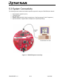
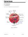
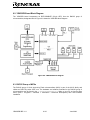
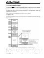
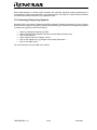
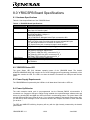
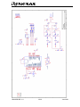
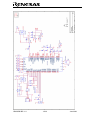
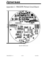
.
Powerful Processors – Easy to Use™
YR8CSPB
Subatomic
Particle Board
User’s Manual
Rev. 1.1
June 2008
www.renesas.com
Table of Contents
1.0 Preface ................................................................................................................................................... 3
1.1. Cautions............................................................................................................................................. 3
1.2. Trademarks........................................................................................................................................ 3
1.3. Copyright ........................................................................................................................................... 3
2.0 Introduction ............................................................................................................................................. 3
3.0 Contents of Product Package................................................................................................................. 4
3.1. YR8CSPB Quick Start Kit Item List ................................................................................................... 4
3.1.1. DVD-ROM ................................................................................................................................... 4
4.0 Limited Guarantee and Support ............................................................................................................. 5
5.0 System Connectivity ............................................................................................................................... 6
5.1. Host Computer Requirements ........................................................................................................... 7
5.2. YR8CSPB Board ............................................................................................................................... 7
5.3. Software Development Tools ............................................................................................................ 7
5.3.1. HEW (High-performance Embedded Workshop)........................................................................ 7
5.3.2. NC30WA Evaluation Version C Compiler ................................................................................... 7
5.3.3. HEW Debug Interface ................................................................................................................. 7
5.3.4. Flash Development Toolkit.......................................................................................................... 7
6.0 Hardware ................................................................................................................................................ 8
6.1. YR8CSPB Board ............................................................................................................................... 8
6.2. YR8CSPB Board Block Diagram....................................................................................................... 9
6.3. R8C/25 Group of MCUs .................................................................................................................... 9
7.0 System Operation & Limitations ........................................................................................................... 10
7.1. Kernel (ROM Monitor) Introduction.................................................................................................. 10
7.2. Pin and Peripheral Limitations......................................................................................................... 11
7.3. Memory Map.................................................................................................................................... 11
7.4. Register Operation Limitations ........................................................................................................ 12
7.5. Limitations on Interrupts – Vectors that Reside in the Hardware Vector Table .............................. 12
7.6. Stop or Wait Mode Limitations......................................................................................................... 12
7.7. User Program’s Real-Time Capability (Very Important – Please Read) ......................................... 12
7.8. Performing Debug Using Symbols .................................................................................................. 13
8.0 YR8CSPB Board Specifications ........................................................................................................... 14
8.1. Hardware Specifications.................................................................................................................. 14
8.2. YR8CSPB Status LED..................................................................................................................... 14
8.3. Power Supply Requirements ........................................................................................................... 14
8.4. Power-Up Behavior.......................................................................................................................... 14
8.5. Operating Environment.................................................................................................................... 15
Appendix A. Expansion Headers................................................................................................................ 16
Appendix B. Board Schematic & BOM ....................................................................................................... 17
Appendix C. YR8CSPB Printed Circuit Board............................................................................................ 20
YR8CSPB SBP V0.1
December 2007
1.0 Preface
1.1. Cautions
This document may, wholly or partially, be subject to change without notice.
All rights reserved. No one is permitted to reproduce or duplicate, in any form, a part of or this entire
document without the written permission of Renesas Technology Corporation.
1.2. Trademarks
All brand or product names used in this manual are trademarks or registered trademarks of their
respective companies or organizations.
1.3. Copyright
© Renesas Technology Corporation. 2007. All rights reserved.
Website: http://www.renesas.com
2.0 Introduction
The Renesas YR8CSPB Subatomic Particle Board (SPB) is a low-cost development environment for
evaluating R8C/Tiny series microcontrollers (MCU) and Renesas software development tools.
The included interactive Flash Video Tutorials teach you how to install and use the Renesas software
development tools.
The kit comes with a complete software development tool chain for Renesas MCUs, including Highperformance Embedded Workshop (HEW), which consists of Integrated Development Environment (IDE),
Graphical User Interface (GUI) and Software Debugger; NC30WA C-compiler, assembler and linker; and
Flash Development Toolkit (FDT) programming software.
The YR8CSPB board features on-board in-circuit debugging and programming support, eliminating the
need for an external In-Circuit Debug (ICD) unit. All that is required for in-circuit debugging and
programming with the YR8CSPB is a USB connection to a PC and the included development tool
software.
A real-time, source-level debug environment is implemented using the HEW software debug interface in
conjunction with the YR8CSPB board. The Flash Development Toolkit Programmer software allows insystem programming of the YR8CSPB board’s R5F21258SNFP Flash MCU.
The YR8CSPB board features an R8C/25 group MCU, switch, LEDs, photo sensor, serial external Flash
and audio amplifier circuit for user experiments. Example application code and peripheral device
initialization code are provided on DVD-ROM.
This manual provides the technical details of the YR8CSPB hardware. The Quick Start Guide and Flash
Video tutorials provide details on the software installation and usage of the debugging environment.
YR8CSPB SBP V1.1
3/ 20
June 2008
3.0 Contents of Product Package
This section describes the contents of the YR8CSPB product package. When unpacking your YR8CSPB
Kit, please check to see that all items listed below are included.
3.1. YR8CSPB Quick Start Kit Item List
Table 3-1 lists the items included in the YR8CSPB.
Table 3-1 YR8CSPB Item List
Item Name
YR8CSPB Board
3′ Mini USB Cable
Stereo Headphones
DVD-ROM
Quantity
1
1
1
1
Remarks
R8C/Tiny SPB with integrated in-circuit debugging and
programming support
Connects YR8CSPB board to Host PC
Connects to YR8CSPB board headphone jack
Auto-install program
HEW (IDE & debugger)
NC30WA (C-compiler, assembler, and linker)
Flash Development Toolkit Programming Software
USB drivers
Manuals
Tutorials
Sample programs
Renesas WOW Installer and Player
3.1.1. DVD-ROM
The DVD-ROM contains the electronic manuals and software necessary for developing programs.
Your computer must have a web browser — like Mozilla Firefox, Netscape® Browser or Microsoft®
Internet Explorer — to view the help files, and Adobe® Acrobat® Reader® to view the manuals.
Insert the enclosed DVD into your computer and the installer should auto-start. The installer program
will create C:\Renesas and C:\Workspace folders on your machine. NC30WA, Documentation
and sample code are installed in the C:\Renesas folder. HEW and Flash Development Toolkit
programming software are installed in the C:\Program Files\Renesas folder by default.
If the installer program does not start, browse to the DVD’s root folder and double-click on
SPB-installer.exe to start the installation.
See the QuickStart Guide for more details.
YR8CSPB SBP V1.1
4/ 20
June 2008
4.0 Limited Guarantee and Support
Renesas Technology America, Inc., warrants the YR8CSPB to be free from component or assembly
defects for a period of 180 days from the date of purchase. Settlement is limited to repair or replacement
of the product only. Renesas Technology America, Inc., does not assume any liability arising out of the
application or use of any product, circuit or procedure described herein. No other liability or warranty
applies, expressed or implied. Software warranty is limited to replacement of the DVD only. While every
attempt has been made to ensure accurate documentation, Renesas Technology America, Inc., cannot
be held responsible for errors or omissions, and reserves the right to make changes without prior notice.
Support for the YR8CSPB kit is provided via the following channels:
1. Renesas website: http://www.america.renesas.com/spb
2. Online User Forums , FAQs, technical papers, downloads and more at http://renesasrulz.com
3. Renesas Technical Support Center, email at [email protected]
General information on Renesas Microcontrollers can be found at the following URL:
http://www.renesas.com
YR8CSPB SBP V1.1
5/ 20
June 2008
5.0 System Connectivity
The following lists the hardware and software products required for using the YR8CSPB Quick Start Kit.
•
•
•
•
•
Host Computer (supplied by user)
YR8CSPB Board
Mini USB cable
Software Tools (HEW IDE, NC30 Compiler/Linker, Flash Development Toolkit Programmer)
Optional Hardware: Supplied Stereo Headphones or amplified speaker(s).
Figure 5-1: YR8CSPB System Connectivity
YR8CSPB SBP V1.1
6/ 20
June 2008
5.1. Host Computer Requirements
The minimum requirement to be able to use the software that comes with the YR8CSPB is a PC with a
USB port and Microsoft Windows XP or Vista.
5.2. YR8CSPB Board
The YR8CSPB board provides an evaluation and development environment for the R8C/Tiny series
MCUs. See section “6.0 Hardware” for more details.
5.3. Software Development Tools
The installer program installs all the development tools. For details on installation, see the QuickStart
Guide. A brief description of all the included tools follows. Please refer to the individual tool manuals for
detailed information.
5.3.1. HEW (High-performance Embedded Workshop)
HEW provides a Graphical User Interface (GUI) that integrates the software development tools and
includes the C-compiler, assembler, linker, debugger and editor.
5.3.2. NC30WA Evaluation Version C Compiler
The evaluation version of the NC30WA C-compiler is provided with the same functionality as the
commercial version except that link size will be restricted to 64 Kbytes after 60 days from when you
begin using the compiler. Contact your local sales representative if you wish to purchase a full license.
5.3.3. HEW Debug Interface
HEW communicates with a kernel (i.e. a ROM monitor program) on the target MCU through the ICD.
This debug interface provides a highly efficient evaluation environment. Features include:
•
•
•
•
•
Source-level debugging for assembly and C language
Single-step command (unlimited breakpoints)
Run command with 2 breakpoints* for the R8C/25
RAM monitor function
C variable “watch” window
*Note: The number of breakpoints will vary depending on the R8C/Tiny Flash MCU used.
5.3.4. Flash Development Toolkit
The Flash Development Toolkit Programmer application provides In-System Programming capability
for the starter kit or any target board using an M16C family Flash MCU (e.g. R8C, M16C, M32C).
Please see the Flash Development Toolkit User Guide for more details.
YR8CSPB SBP V1.1
7/ 20
June 2008
6.0 Hardware
6.1. YR8CSPB Board
Figure 6-1 shows the YR8CSPB Board with major components identified.
Figure 6-1: YR8CSPB Board
YR8CSPB SBP V1.1
8/ 20
June 2008
6.2. YR8CSPB Board Block Diagram
The YR8CSPB board incorporates an R5F21258SNFP (52-pin QFP) from the R8C/25 group of
microcontrollers, designated as U6. Figure 6-2 shows the YR8CSPB block diagram.
Figure 6-2: YR8CSPB Block Diagram
6.3. R8C/25 Group of MCUs
The R8C/25 group of 16-bit single-chip Flash microcontrollers (MCU) is part of the M16C family and
utilizes an R8C/Tiny series CPU core. The hardware and software manuals for the R8C/25 group of
microcontrollers can be found in the C:\Renesas\YR8CSPB\Docs folder on your PC or from the Start
menu (Start > Programs > Renesas > YR8CSPB > Document Descriptions) after SPB software
installation.
YR8CSPB SBP V1.1
9/ 20
June 2008
7.0 System Operation & Limitations
The YR8CSPB board provides sophisticated debugging features at a low cost via its on-board in-circuit
debugging and programming circuitry (ICD).
For R8C/Tiny boards without on-board debugging/programming circuitry, Renesas offers the functionally
equivalent, standalone E8 in-circuit debugger/programmer. You can find detailed information on the E8
and its functionality in the E8 Emulator User’s Manual, which you can view via the HEW Manual Navigator.
The YR8CSPB board does have some limitations when used with the HEW software debugger and the
board’s ICD circuit. Section 7.1 introduces the kernel (ROM monitor) program and its purpose. The
limitations when this kernel is running with the user program are listed in Table 7-1.
Table 7-1: System Limitations when Debugging
Item
Please Refer To
7.2 Pin and Peripheral Limitations
7.3 Memory Map
User Limitations
7.4 Register Operation Limitations
7.5 Limitations on Interrupts – Vectors that Reside in the Hardware
Vector Table
7.6 Stop or Wait Mode Limitations
The kernel cannot be run in STOP or WAIT modes. Do not use these
Debugger Limitations
modes when debugging your program
7.7 User Program’s Real-Time Capability
7.1. Kernel (ROM Monitor) Introduction
During debug, a small program called a kernel is uploaded to the R8C/25 (R5F21258SNFP) MCU. The
kernel communicates with HEW through the ICD portion of the YR8CSPB board regarding MCU status
during user code debugging operations.
There are no special steps required in the user program to make use of the ICD portion. The operation of
the kernel is transparent to the user, but there are some limitations. These are discussed from section 7.2
onward.
After starting a HEW debug session, the ICD uploads the kernel to the R8C/25 if it does not already exist
(e.g. on a blank device or a device that was programmed with the Flash Development Toolkit
Programmer). After downloading the kernel, the R8C/25 is ready to download user code.
Connecting the YR8CSPB board without starting HEW will not affect the signal lines connected between
the ICD MCU (HD64F2215RUBR) and the R8C/25; the ICD MCU keeps the signal lines in highimpedance state. The ICD MCU only drives the pins after HEW or the Flash Development Toolkit
software attempts to connect.
After completing program debug and verification with HEW, you can create an image of your code in Intel
(.hex) or Motorola (.mot) file formats. This image can be programmed into the R8C/25 using the Flash
Development Toolkit programming software. This procedure erases the kernel and leaves only the user
program.
YR8CSPB SBP V1.1
10/ 20
June 2008
7.2. Pin and Peripheral Limitations
The Mode and Reset pins are used for communication between the R8C/25 kernel on the YR8CSPB
board and the board’s ICD MCU (HD64F2215RUBR). Do not connect these pins to any other circuit, as
they cannot be used in the user program while using the Debugger.
The E8 debugger uses up to 8 bytes of the stack pointer during a user program break. Therefore, set
aside 8 bytes for the stack area.
UART1 is used by the E8 debugger. Do not use UART1 in the user program.
7.3. Memory Map
The amount and locations of memory used by the kernel on the YR8CSPB board’s R8C/25 MCU are
shown in Figure 7-1.
Figure 7-1: R5F21258SNFP Memory Map with the Kernel Program
When ‘Advanced Settings’ are enabled in the Emulator Settings Dialog box in High-performance
Embedded Workshop, a dialog box is displayed that allows you to place the kernel anywhere in the
available user Flash Data or Program memory. Specify an area that is not used by your application
software.
YR8CSPB SBP V1.1
11/ 20
June 2008
7.4. Register Operation Limitations
Table 7-2 lists the limitations on register operation. The registers are inhibited from any modification. If
register contents are modified in any way, kernel operation cannot be guaranteed.
Table 7-2: Limitations on Register Operation
Register Name
Address Match Interrupt Registers (RMAD0, RMAD1,
AIER)
UART1 Transmit/Receive Mode Register (U1MR)
UART1 Transmit/Receive Control Register 0 (U1C0)
UART1 Transmit/Receive Control Register 1 (U1C1)
UART1 Bit Rate Register (U1BRG)
UART1 Transmit Buffer Register (U1TB)
UART1 Receive Buffer Register (U1RB)
Port Mode Register (PMR)
Protect Register (PRCR)
High-speed on-chip oscillator control register 0 (FRA0)
High-speed on-chip oscillator control register 1 (FRA1)
Flash memory control register 4 (FMR4)
Restriction
Do not change
Do not change.
Do not change.
Do not write to this register.
Do not read this register.
Do not change Bit4; use read-modify-write
only instructions (BSET, BCLR, AND, OR,
etc.) when accessing the PMR register.
Do not change Bit0; use read-modify-write
only instructions.
Do not change Bit0; use read-modify-write
only instructions
Do not change.
Do not change Bit7; use read-modify-write
only instructions.
7.5. Limitations on Interrupts – Vectors that Reside in the Hardware Vector Table
Table 7-3 lists the limitations on hardware interrupt (i.e. fixed) vector addresses.
Table 7-3: Interrupt Vector Addresses
Interrupt Cause
R8C/25 Vector Address
Undefined
FFFDCh ~ FFFDFh
Overflow
FFFE0h ~ FFFE3h
BRK Instruction
FFFE4h ~ FFFE7h
Address Match
FFFE8h ~ FFFEBh
Single-step
FFFECh ~ FFFEFh
Watchdog Timer
FFFF0h ~ FFFF3h
Address Break
FFFF4h ~ FFFF7h
Reserved
FFFF8h ~ FFFFBh
RESET
FFFFCh ~ FFFFFh
Kit Specification
User available
User available
User inhibited
User inhibited
User inhibited
User available
User inhibited
User inhibited
Reset vector
7.6. Stop or Wait Mode Limitations
The kernel cannot be run in STOP or WAIT modes. Do not use these modes when debugging your
program.
7.7. User Program’s Real-Time Capability (Very Important – Please Read)
Please be aware that while the kernel is in a “STOP” state, the hardware peripherals will continue to run.
Therefore, interrupts may not be serviced properly. In addition, the watchdog timer will not be serviced
and will likely time out if active.
YR8CSPB SBP V1.1
12/ 20
June 2008
When RAM Windows or Variable Watch Windows are refreshed, significant target processing time is
consumed during which user application code is not executed. Use caution in using refreshing windows,
as it affects the real-time behavior of your application code.
7.8. Performing Debug Using Symbols
Normally when a new project is created using HEW, debugging symbols are enabled. If you are unable to
view the source properly during debug, add the debug option [-g] in HEW before compiling the programs.
To enable the [-g] option, perform the following:
•
•
•
•
•
•
Open the workspace and project in HEW.
Select ‘Renesas M16C Standard Toolchain’ from the Build pull-down menu.
Click on the [Link] tab.
Select ‘Output’ under the ‘Category’ list box.
Click on the checkbox for [-g] ‘Outputs source debug information…’.
Click on the <OK> button.
For more information, see the HEW user’s manual.
YR8CSPB SBP V1.1
13/ 20
June 2008
8.0 YR8CSPB Board Specifications
8.1. Hardware Specifications
Table 8-1 lists the specifications of the YR8CSPB Board.
Table 8-1: YR8CSPB Board Specifications
Item
Specification
MCU
R5F21258SNFP
Clocks
Main Clock: 20 MHz resonator, high- or low-speed on-chip oscillator
Sub Clock: 32.768 kHz crystal
Memory
RAM: 3Kbytes
High E/W Data Block: 1Kbyte × 2
Flash ROM: 64Kbytes
[U9]: AT26DF081A: 8Megabit Serial Flash, connected to SIO
Connectors
[E8_SW1]: 2-pin solder pads to mount Boot Mode header.
[MCU_IO]: 9-pin single row solder pads to access selected MCU pins
[J1]: Mini USB connector for connection of board to PC
[J2]: Stereo Phone jack, connected to board’s audio amplifier
Switches
[S1]: Pushbutton (connected to P4_5/ INT0 )
LEDs
[D1] (Amber): AMB User LED, connected to P2_1
[D2] (Green): Debugger Status/Power
[D3] (Green): GRN User LED, connected to P2_2
[D4] (Orange): ORG User LED, connected to P2_3
[D5] (Red): RED User LED, connected to P2_0
Photo Sensor
[R17]: Connected to AN1 analog input
Audio Amplifier
[U8]: LM4808 Stereo Amplifier, connected to PWM Timer outputs TRDIOD1
and TRDIOC1
8.2. YR8CSPB Status LED
The green Status LED (D2) indicates operating status of the YR8CSPB board. The board’s
HD64F2215RUBRHP MCU that controls the In-Circuit Debugging and Programming functionality of the
board also controls the LED. The LED is on when the board is connected to a USB port and receives
power.
8.3. Power Supply Requirements
The YR8CSPB Board is powered by the USB bus. It will draw about 50mA with no LEDs on.
8.4. Power-Up Behavior
The audio example tutorial code is pre-programmed into the Renesas R8C/25 microcontroller. If
connected to a computer’s USB port, without having installed the required Renesas software tools and
drivers, the board’s RED and AMB user LED’s will flash in an alternating pattern. The green Status LED
and the GRN and ORG user LEDs will be on. If you connect a headset to the board’s stereo phone jack,
you will hear an audio message “Do not connect this board to the computer until after we have instructed
you to do so…”.
The RED and AMB LED’s blinking frequency will vary with the light intensity measured by the board’s
photo sensor.
YR8CSPB SBP V1.1
14/ 20
June 2008
8.5. Operating Environment
Table 8-2 lists the environmental conditions for using and storing the YR8CSPB board. Store the board in
a conductive bag inside the original factory packaging.
Table 8-2: Operating and Storage Environments
Environmental Condition
Ambient Temperature
Operating
0 to 55°C
(No corrosive gas allowed)
Storage
−30 to 75°C
(No corrosive gas allowed)
YR8CSPB SBP V1.1
15/ 20
Ambient Humidity
30 to 80% (non-condensing)
30 to 80% (non-condensing)
June 2008
Appendix A. Expansion Headers
The R5F21258SNFP MCU on the YR8CSPB target board is housed in a 52-pin QFP package. Pin 1 of
the package is identified by the number ‘1’ on the board’s top silkscreen. The MCU_I/O solder pads,
located below the “YR8CSPB” silkscreen print, provide access to some of the MCU’s pins. You can use
MCU_I/O as test points to check MCU signals or, by mounting your own header, to connect your own
external circuitry. The silkscreen identifying the connectors is at the top of the YR8CSPB board. The
following table shows the mapping of MCU_I/O solder pads to MCU pins and signal names.
Vcc
AN4
AN5
TxD0
RxD0
CLK0
KI3/AN11
52
QFP
MCU Pin
12
48
49
24
23
22
25
TRAIO/INT1
21
GND
10
MCU_I/O Pin
YR8CSPB SBP V1.1
MCU Function
Vcc/AVcc
P03/AN4
P02/AN5
P14/TxD0
P15/RxD0
P16/CLK0
P13/ KI3 / AN11
P17/TRAIO/ INT1
Vss/AVss
16/ 20
June 2008
Appendix B. Board Schematic & BOM
The circuit board schematic and Bill-Of-Materials (BOM) are available as separate PDF documents. They
can be viewed via Start > Programs > Renesas > YR8CSPB > Board Hardware, or by browsing to the
folder C:\Renesas\YR8CSPB\Docs and opening the files:
YR8CSPB_RevC.pdf
YR8CSPB_BOM_RevC.pdf
YR8CSPB SBP V1.1
17/ 20
June 2008
YR8CSPB SBP V1.1
18/ 20
June 2008
YR8CSPB SBP V1.1
19/ 20
June 2008
Appendix C. YR8CSPB Printed Circuit Board
3.500 inch
YR8CSPB
Figure E-1: PCB Top View
YR8CSPB SBP V1.1
20/ 20
June 2008