1
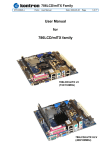
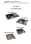
KTQM67/mITX
KTQM67/Flex
KTQM67/ATXP
KTQM67 Users Guide
KTD-N0819-G
If it’s embedded, it’s Kontron
KTD-N0819-G
Page 2
Document details
Document revision history.
Revision
Date
G
July 10 2012
F
May 18 2012
E
Jan 19 2012
D
Dec 28 2011
A -C
0
Aug 16 2011
th
Jun 8 2011
By
th
MLA
th
MLA
th
MLA
th
MLA
th
MLA
MLA
Comment
Added USB port/EHCI relation. Added normal beep info. Added
info about backside label. Ivy Bridge support added. Note for
support of PCIe x2.
Added notes in chapter Power Consumption. Correction of EDP
connector pin order. Added info, miniPCIe USB signals not
supported. Added OS support. Added DP extension cable. SPI
Recovery procedure improved. BIOS part added. Chapter 9
tables finished.
Correction to SPI description. Added information about
Processor dependent support of SODIMM slots. Changed
SODIMM numbers.
Sspec no. correction. Added i3-2320E. LPT not on mITX. Added
SPI connector details. Added KTQM67/ATXP pictures and
related data.
Comments removed in revision G.
Preliminary version
Copyright Notice:
Copyright 2011, KONTRON Technology A/S, ALL RIGHTS RESERVED.
No part of this document may be reproduced or transmitted in any form or by any means, electronically
or mechanically, for any purpose, without the express written permission of KONTRON Technology A/S.
Trademark Acknowledgement:
Brand and product names are trademarks or registered trademarks of their respective owners.
Disclaimer:
KONTRON Technology A/S reserves the right to make changes, without notice, to any product,
including circuits and/or software described or contained in this manual in order to improve design
and/or performance.
Specifications listed in this manual are subject to change without notice. KONTRON Technology
assumes no responsibility or liability for the use of the described product(s), conveys no license or title
under any patent, copyright, or mask work rights to these products, and makes no representations or
warranties that these products are free from patent, copyright, or mask work right infringement, unless
otherwise specified. Applications that are described in this manual are for illustration purposes only.
KONTRON Technology A/S makes no representation or warranty that such application will be suitable
for the specified use without further testing or modification.
Life Support Policy
KONTRON Technology’s PRODUCTS ARE NOT FOR USE AS CRITICAL COMPONENTS IN LIFE
SUPPORT DEVICES OR SYSTEMS WITHOUT EXPRESS WRITTEN APPROVAL OF THE GENERAL
MANAGER OF KONTRON Technology A/S.
As used herein:
Life support devices or systems are devices or systems which, (a) are intended for surgical implant into
body, or (b) support or sustain life and whose failure to perform, when properly used in accordance with
instructions for use provided in the labelling, can be reasonably expected to result in significant injury to
the user.
A critical component is any component of a life support device or system whose failure to perform can
be reasonably expected to cause the failure of the life support device or system, or to affect its safety or
effectiveness.
KTQM67 Users Guide
KTD-N0819-G
Page 3
Document details
KONTRON Technology Technical Support and
Services
If you have questions about installing or using your KONTRON Technology Product, check this User’s
Manual first – you will find answers to most questions here. To obtain support, please contact your local
Distributor or Field Application Engineer (FAE).
Before Contacting Support: Please be prepared to provide as much information as possible:
• CPU Board
1. Type.
2. Part Number (find PN on label)
3. Serial Number if available (find SN on label)
• Configuration
1. CPU Type, Clock speed
2. DRAM Type and Size.
3. BIOS Revision (Find the Version Info in the BIOS Setup).
4. BIOS Settings different than Default Settings (Refer to the BIOS Setup Section).
• System
1. O/S Make and Version.
2. Driver Version numbers (Graphics, Network, and Audio).
3. Attached Hardware: Harddisks, CD-rom, LCD Panels etc.
Warranty
KONTRON Technology warrants its products to be free from defects in material and workmanship
during the warranty period. If a product proves to be defective in material or workmanship during the
warranty period, KONTRON Technology will, at its sole option, repair or replace the product with a
similar product.
Replacement Product or parts may include remanufactured or refurbished parts or components.
The warranty does not cover:
1. Damage, deterioration or malfunction resulting from:
A. Accident, misuse, neglect, fire, water, lightning, or other acts of nature, unauthorized product
modification, or failure to follow instructions supplied with the product.
B. Repair or attempted repair by anyone not authorized by KONTRON Technology.
C. Causes external to the product, such as electric power fluctuations or failure.
D. Normal wear and tear.
E. Any other causes which does not relate to a product defect.
2. Removal, installation, and set-up service charges.
Exclusion of damages:
KONTRON TECHNOLOGY LIABILITY IS LIMITED TO THE COST OF REPAIR OR REPLACEMENT
OF THE PRODUCT. KONTRON TECHNOLOGY SHALL NOT BE LIABLE FOR:
1. DAMAGE TO OTHER PROPERTY CAUSED BY ANY DEFECTS IN THE PRODUCT,
DAMAGES BASED UPON INCONVENIENCE, LOSS OF USE OF THE PRODUCT, LOSS OF
TIME, LOSS OF PROFITS, LOSS OF BUSINESS OPPORTUNITY, LOSS OF GOODWILL,
INTERFERENCE WITH BUSINESS RELATIONSHIPS, OR OTHER COMMERCIAL LOSS,
EVEN IF ADVISED OF THEIR POSSIBILITY OF SUCH DAMAGES.
2. ANY OTHER DAMAGES, WHETHER INCIDENTAL, CONSEQUENTIAL OR OTHERWISE.
3. ANY CLAIM AGAINST THE CUSTOMER BY ANY OTHER PARTY.
KTQM67 Users Guide
KTD-N0819-G
Page 4
Contents
Contents
Introduction ........................................................................................... 7
1
Installation procedure .................................................................... 8
1.1
Installing the board ........................................................................................................................ 8
1.2
Requirement according to IEC60950 ............................................................................................ 9
2
System Specification ................................................................... 10
2.1
Component main data ................................................................................................................. 10
2.2
System overview ......................................................................................................................... 14
2.3
Processor Support Table............................................................................................................. 15
2.4
System Memory support ............................................................................................................. 18
2.5
KTQM67 Graphics Subsystem .................................................................................................... 19
2.5.1 Intel® HD Graphics 3000 ........................................................................................................... 19
2.6
Power Consumption .................................................................................................................... 20
3
Connector Locations ................................................................... 28
3.1
KTQM67/mITX – frontside........................................................................................................... 28
3.2
KTQM67/mITX – IO Bracket area
3.3
KTQM67/mITX - backside ........................................................................................................... 29
3.4
KTQM67/Flex .............................................................................................................................. 30
3.5
KTQM67/Flex - backside ............................................................................................................. 31
3.6
KTQM67/ATXP ............................................................................................................................ 32
3.7
KTQM67/ATXP - backside .......................................................................................................... 33
4
Connector Definitions .................................................................. 34
5
IO-Area Connectors ..................................................................... 35
.......................................................................................... 29
5.1
Display connectors (IO Area) ...................................................................................................... 35
5.1.1 DVI Connector (DVI-I) (J41) ....................................................................................................... 35
5.1.2 DP Connectors (DP0/DP1) (J40/J39) ........................................................................................ 36
5.2
Ethernet Connectors ................................................................................................................... 37
5.3
USB Connectors (IO Area) .......................................................................................................... 38
5.3.1 USB Connector 0/1 (USB0/1) .................................................................................................... 38
5.3.2 USB Connector 2/3 (USB2/3) .................................................................................................... 39
5.3.3 USB Connector 4/5 (USB4/5) .................................................................................................... 39
5.4
Audio Connector (IO Area) .......................................................................................................... 40
6
Internal Connectors ..................................................................... 41
6.1
Power Connector (ATX/BTXPWR).............................................................................................. 41
6.2
Fan Connectors (FAN_CPU) (J28) and (FAN_SYS) (J29) ......................................................... 42
6.3
PS/2 Keyboard and Mouse connector (KBDMSE) (J27) ............................................................ 43
6.4
Display connectors (Internal)....................................................................................................... 44
6.4.1 eDP connector (EDP) (J38) ....................................................................................................... 44
KTQM67 Users Guide
KTD-N0819-G
6.4.2
6.5
Page 5
LVDS Flat Panel Connector (LVDS) (J20) ................................................................................. 45
SATA (Serial ATA) Disk interface (J21 – J26) ............................................................................ 46
6.6
USB Connectors (USB) ............................................................................................................... 47
6.6.1 USB Connector 6/7 .................................................................................................................... 47
6.6.2 USB Connector 8/9 (USB8/9) (J10) ........................................................................................... 47
6.6.3 USB Connector 10/11 (USB10/11) (J11) ................................................................................... 47
6.6.4 USB Connector 12/13 (USB12/13) (J12) ................................................................................... 48
6.7
Firewire/IEEE1394 connectors (J13,J14).................................................................................... 49
6.7.1 IEEE1394 connector (IEEE1394_0) (J14) ................................................................................. 49
6.7.2 IEEE1394 connector (IEEE1394_1) (J13) ................................................................................. 49
6.8
Serial COM1 – COM4 Ports (J15, J16, J17, J18) ....................................................................... 50
6.9
LPT (Line Print Terminal – Parallel port) (J44)............................................................................ 51
6.10 Audio Connectors ........................................................................................................................ 52
6.10.1 CDROM Audio Input (CDROM) (J3) .......................................................................................... 52
6.10.2 Line2 and Mic2 ........................................................................................................................... 52
6.10.3 Audio Header Connector (AUDIO_HEAD) (J31) ....................................................................... 53
6.11
Front Panel Connector (FRONTPNL) (J19) ................................................................................ 54
6.12
Feature Connector (FEATURE) (J30) ......................................................................................... 55
6.13
Clear CMOS Jumper (J37) .......................................................................................................... 57
6.14
SPI Recover Jumper (J4) ............................................................................................................ 58
6.15
SPI Connector (SPI) (J5)............................................................................................................. 58
6.16
XDP-CPU (Debug Port for CPU) (J32) ....................................................................................... 59
6.17
XDP-PCH (Debug Port for Chipset) (J33) ................................................................................... 60
7
Slot Connectors (PCIe, miniPCIe, PCI) ....................................... 61
7.1
PCIe Connectors ......................................................................................................................... 61
7.1.1 PCI-Express x16 Connector (PCIe x16) .................................................................................... 61
7.1.2 miniPCI-Express mPCIe0 (J34) ................................................................................................. 63
7.1.3 miniPCI-Express mPCIe1 (J35) ................................................................................................. 64
7.1.4 PCI-Express x1 Connector (PCIe x1) (J36) ............................................................................... 65
7.2
7.2.1
7.2.2
PCI Slot Connectors ................................................................................................................... 66
Signal Description – PCI Slot Connector ................................................................................... 67
KTQM67 PCI IRQ & INT routing ................................................................................................ 68
8
On-board - & mating connector types ........................................ 69
9
System Resources ....................................................................... 70
9.1
Memory Map ............................................................................................................................... 70
9.2
PCI Devices ................................................................................................................................. 71
9.3
Interrupt Usage ............................................................................................................................ 72
9.4
IO Map ......................................................................................................................................... 73
10 BIOS .............................................................................................. 75
10.1
Main ............................................................................................................................................. 75
10.2 Advanced .................................................................................................................................... 76
10.2.1 Advanced - PCI Subsystem Settings ....................................................................................... 77
10.2.2 Advanced - APCI Settings ....................................................................................................... 80
10.2.3 Advanced - Trusted Computing ............................................................................................... 81
10.2.4 Advanced - CPU Configuration ................................................................................................ 82
10.2.5 Advanced - SATA Configuration .............................................................................................. 84
10.2.6 Advanced - Intel TXT (LT) Configuration ................................................................................. 88
10.2.7 Advanced - AMT Configuration ................................................................................................ 89
10.2.8 Advanced - Acoustic Management Configuration.................................................................... 91
10.2.9 Advanced - USB Configuration ................................................................................................ 92
KTQM67 Users Guide
KTD-N0819-G
10.2.10
10.2.11
10.2.12
10.2.13
10.2.14
10.2.15
10.2.16
10.2.17
Advanced
Advanced
Advanced
Advanced
Advanced
Advanced
Advanced
Advanced
Page 6
-
SMART Settings ........................................................................................... 93
Super IO Configuration ................................................................................. 94
LAN Configuration ...................................................................................... 100
Displayblock Setup ..................................................................................... 102
Voltage Monitor........................................................................................... 103
Hardware Health Configuration .................................................................. 104
Serial Port Console Redirection ................................................................. 106
CPU PPM Configuration ............................................................................. 110
10.3 Chipset ...................................................................................................................................... 111
10.3.1 PCH-IO Configuration .............................................................................................................. 112
10.3.2 System Agent (SA) Configuration ............................................................................................ 117
10.4 Boot ........................................................................................................................................... 128
10.4.1 CSM parameters ...................................................................................................................... 130
10.5 Security...................................................................................................................................... 131
10.5.1 Security Boot Policy ................................................................................................................. 132
10.5.2 Key Management ..................................................................................................................... 134
10.6
Save & Exit ................................................................................................................................ 135
11 AMI BIOS Beep Codes ............................................................... 136
12 OS Setup ..................................................................................... 137
KTQM67 Users Guide
KTD-N0819-G
Page 7
Introduction
Introduction
This manual describes the KTQM67/mITX, KTQM67/Flex and KTQM67/ATXP boards made by
KONTRON Technology A/S. The boards will also be denoted KTQM67 family if no differentiation is
required.
nd
rd
The KTQM67 boards, all based on the QM67 chipset, support 2 and 3 generation Intel® i7 -, i5 -, i3
2Core and 4Core processor and the Celeron B810 2Core, see “Processor Support Table for more
specific details.
The KTQM67 family consist on members having different form factors, and the same functionality
except for the functions listed in the table below.
KTQM67 variants
Format
PCI
LPT
SODIMM Sockets
Single +12V Power Supply
KTQM67/mITX
mITX
-
-
2
Yes
4
No
4
No
KTQM67/Flex
Flex
3
1
KTQM67/ATXP
ATX
6
1
Use of this Users Guide implies a basic knowledge of PC-AT hard- and software. This manual is
focused on describing the KTQM67 board’s special features and is not intended to be a standard PC-AT
textbook.
New users are recommended to study the short installation procedure stated in the following chapter
before switching-on the power.
All configuration and setup of the CPU board is either done automatically or manually by the user via
the CMOS setup menus. Only exception is the Clear CMOS jumper.
KTQM67 Users Guide
KTD-N0819-G
Page 8
Installation procedure
1 Installation procedure
1.1 Installing the board
To get the board running, follow these steps. If the board shipped from KONTRON has already
components like RAM, CPU and cooler mounted, then relevant steps below, can be skipped.
1. Turn off the PSU (Power Supply Unit)
!
Warning: Turn off PSU (Power Supply Unit) completely (no mains power connected to the
PSU) or leave the Power Connectors unconnected while configuring the board. Otherwise
components (RAM, LAN cards etc.) might get damaged. If not using KTQM67/mITX and single
12V power input make sure PSU has 3.3V monitoring watchdog (standard ATX PSU feature),
running the board without 3.3V will damage the board within minutes.
2. Insert the DDR3 DIMM 204pin SODIMM module(s)
Be careful to push it in the slot(s) before locking the tabs. For a list of approved DDR3 SODIMMs
contact your Distributor or FAE. See also chapter “System Memory Support”.
3. Install the processor
The CPU is keyed and will only mount in the CPU socket in one way. Use suitable screwdriver to
open/ close the CPU socket. Refer to supported processor overview for details.
4. Cooler Installation
Use heat paste or adhesive pads between CPU and cooler and connect the Fan electrically to the
FAN_CPU connector.
5. Connecting Interfaces
Insert all external cables for hard disk, keyboard etc. A monitor must be connected in order to be
able change CMOS settings.
6. Connect and turn on PSU
Connect PSU to the board by the ATX/BTXPWR and the 4-pin ATX+12V connectors. For the
KTQM67/mITX alternatively use only the 4-pin ATX+12V connector if single voltage operation (+12V
+/-5%) is requested.
7. Power Button
The PWRBTN_IN must be toggled to start the Power supply; this is done by shorting pins 16
(PWRBTN_IN) and pin 18 (GND) on the FRONTPNL connector (see Connector description). A
“normally open” switch can be connected via the FRONTPNL connector.
8. BIOS Setup
Enter the BIOS setup by pressing the <Del> key during boot up.
Enter Exit Menu and Load Optimal Defaults.
Refer to the “BIOS Configuration / Setup“ section of this manual for details on BIOS setup.
Note: To clear all CMOS settings, including Password protection, move the Clear CMOS jumper in the
Clear CMOS position (with or without power) for ~10 sec. This will Load Failsafe Defaults and make sure
Secure CMOS is disabled.
9. Mounting the board to chassis
!
Warning: When mounting the board to chassis etc. please notice that the board contains
components on both sides of the PCB which can easily be damaged if board is handled
without reasonable care. A damaged component can result in malfunction or no function at all.
When fixing the Motherboard on a chassis it is recommended using screws with integrated washer and
having diameter of ~7mm.
Note: Do not use washers with teeth, as they can damage the PCB and may cause short circuits.
KTQM67 Users Guide
KTD-N0819-G
Installation procedure
Page 9
1.2 Requirement according to IEC60950
Users of KTQM67 family boards should take care when designing chassis interface connectors in order
to fulfil the IEC60950 standard:
When an interface/connector has a VCC (or other power) pin, which is directly connected to a power
plane like the VCC plane:
To protect the external power lines of the peripheral devices, the customer has to take care about:
• That the wires have suitable rating to withstand the maximum available power.
• That the enclosure of the peripheral device fulfils the fire protecting requirements of IEC60950.
Lithium Battery precautions:
CAUTION!
Danger of explosion if battery is incorrectly
replaced.
Replace only with same or equivalent type
recommended by manufacturer.
Dispose of used batteries according
to the manufacturer’s instructions.
ADVARSEL!
Lithiumbatteri – Eksplosionsfare ved fejlagtig
håndtering.
Udskiftning må kun ske med batteri
af samme fabrikat og type.
Levér det brugte batteri tilbage til leverandøren.
VORSICHT!
Explosionsgefahr bei unsachgemäßem
Austausch der Batterie.
Ersatz nur durch den selben oder einen vom
Hersteller empfohlenen gleichwertigen Typ.
Entsorgung gebrauchter Batterien nach
Angaben des Herstellers.
ADVARSEL
Eksplosjonsfare ved feilaktig skifte av batteri.
Benytt samme batteritype eller en tilsvarende
type anbefalt av apparatfabrikanten.
Brukte batterier kasseres i henhold til
fabrikantens
instruksjoner.
VAROITUS
VARNING
Explosionsfara vid felaktigt batteribyte.
Använd samma batterityp eller en ekvivalent
typ som rekommenderas av apparattillverkaren.
Kassera använt batteri enligt fabrikantens
instruktion.
Paristo voi räjähtää, jos se on virheellisesti
asennettu.
Vaihda paristo ainoastaan laltevalmistajan
suosittelemaan
tyyppiin. Hävitä käytetty paristo valmistajan
ohjeiden
mukaisesti.
KTQM67 Users Guide
KTD-N0819-G
Page 10
System Specification
2 System Specification
2.1 Component main data
The table below summarizes the features of the KTQM67/mITX, KTQM67/Flex and KTQM67/ATXP
embedded motherboards.
Form factor
KTQM67/mITX: miniITX (170,18 mm by 170,18 mm)
KTQM67/Flex: Flex-ATX (190,5 mm by 228,6 mm)
KTQM67/ATXP: ATX (190,5 mm by 304,0 mm)
Processor
Support 2 and 3 Generation Intel® Core™ (Sandy Bridge M and Ivy Bridge M
respectively) and Intel® Celeron® processors via Socket G2 (rPGA 988B ) ZIF Socket
• Intel® Core™ i7
• Intel® Core™ i5
• Intel® Core™ i3
• Intel® Celeron® B810
Up to 1333MHz system bus and 2/3/4/6MB internal cache.
Memory
•
•
nd
•
•
rd
DDR3 SODIMM 204pin socket (2 sockets on mITX and 4 sockets on Flex/ATXP)
Support single and dual ranks DDR3 1066/1333/1600MT/s
(PC3-8500/PC3-10600/PC3-12800)
Support system memory from 256MB and up to 4x 8GB (2x 8GB on mITX).
Notes: Only some of the processors support 4 SODIMM slots.
Less than 4GB displayed in System Properties using 32bit OS
(Shared Video Memory/PCI resources is subtracted)
ECC not supported (PGA processors do not support ECC)
Chipset
Intel QM67 PCH (Platform Controller Hub)
• Intel ® VT-d (Virtualisation Technology for Directed I/O)
• Intel ® TXT (Trusted Execution Technology)
• Intel ® vPRO
• Intel ® AMT (Active Management Technology) version 7
• Intel ® AT (Anti-Theft Technology)
• Intel ® HD Audio Technology
• Intel ® RST (Rapid Storage Technology)
• Intel ® RRT (Rapid Recover Technology)
• SATA (Serial ATA) 6Gb/s and 3Gb/s.
• USB revision 2.0
• PCI Express revision 2.0
• ACPI 3.0b compliant
• Dual Display support (Dual Graphic Pipes)
• Blue-ray HD video playback
Security
•
Intel® Integrated TPM 1.2 support
Management
•
Intel® Active Management Technology (Intel® AMT) 7.0
Audio
Audio, 7.1 Channel High Definition Audio Codec using the VIA 1708B codec
• Line-out
• Line-in
• Surround output: SIDE, LFE, CEN, BACK and FRONT
• Microphone: MIC1 and MIC2
• CDROM in
• SPDIF (electrical Interface only)
• On-board speaker (Electromagnetic Sound Generator like Hycom HY-05LF)
KTQM67 Users Guide
KTD-N0819-G
Video
Page 11
System Specification
Intel ® i3, i5 or i7 processor supports Intel ® HD Graphics 3000.
Intel ® Celeron ® Processor B810 supports Intel ® HD Graphics.
eDP (Embedded DisplayPort) directly from processor.
Analogue VGA and digital display ports (DVI, 2x DP, LVDS) via the Mobile Intel ®
QM67 Chipset.
•
•
•
•
•
•
•
•
VGA (analogue panel) via DVI-I (sharing DVI-I connector with DVI-D)
DVI-D (sharing DVI-I connector with analogue VGA)
DP (DisplayPorts) dual, comply with DisplayPort 1.1a specification.
LVDS panel support up to 24 bit, 2 pixels/clock and 1920x1200.
HDMI panel support via DP to HDMI Adapter Converter.
Second VGA panel support via DP to VGA Adapter Converter
Second DVI panel support via DP to DVI Adapter Converter
Dual independent pipes for Mirror and Dual independent display support
(exception is combination LVDS and eDP)
I/O Control
Via ITE IT8516E Embedded Controller and
(both via LPC Bus interface)
Peripheral
interfaces
•
•
•
•
•
•
•
•
•
•
Six USB 2.0 ports on I/O area
Eight USB 2.0 ports on internal pinrows
Two IEEE 1394a-2000 (up to 400M bits/s) on internal pinrows
Four Serial ports (RS232) on internal pinrows
LPT via single in line connector (only KTQM67/Flex and KTQM67/ATXP)
Two Serial ATA-600 IDE interfaces
Four Serial ATA-300 IDE interfaces
RAID 0/1/5/10 support
mSATA via mPCIe_0 connector
PS/2 keyboard and mouse ports via pinrow
LAN
Support
•
1x 10/100/1000Mbits/s LAN (ETHER1) using Intel® Lewisville 82579LM Gigabit
PHY connected to QM67 supporting AMT 7.0
2x 10/100/1000Mbits/s LAN (ETHER2/ETHER3)using Intel® Hartwell 82574L PCI
Express controllers
PXE Netboot supported.
Wake On LAN (WOL) supported
•
•
•
Expansion
Capabilities
•
•
•
•
•
•
•
•
•
•
Winbond W83627DHG I/O Controller
PCI Bus routed to PCI slot(s) (PCI Local Bus Specification Revision 3.0, 33MHz)
o KTQM67/mITX None.
o KTQM67/Flex: 3
o KTQM67/ATXP: 6
PCI-Express slot(s) (PCIe 2.0), for all KTQM67 family members:
o 1 slot PCIe x16
o 1 slot PCIe x1
o 1 slot miniPCI-Express (PCI Express or mSATA signals, no USB signals)
o 1 slot miniPCI-Express (PCI Express signals, no mSATA or USB signals)
SMBus, compatible with ACCES BUS and I2C BUS, (via Feature connector)
SPI bus routed to SPI connector
DDC Bus routed to DVI-I connector
18 x GPIOs (General Purpose I/Os), (via Feature connector)
DAC, ADC, PWM and TIMER (Multiplexed), (via Feature connector)
WAKE UP / Interrupt Inputs (Multiplexed), (via Feature connector)
3 Wire Bus for GPIO Expansion (up to 152 GPIOs), (via Feature connector)
8 bit Timer output, (via Feature connector)
KTQM67 Users Guide
KTD-N0819-G
Hardware
Monitor
Subsystem
•
•
•
•
•
•
Page 12
System Specification
Smart Fan control system, support Thermal® and Speed® cruise for three onboard Fan control connectors: FAN_CPU, FAN_SYS and FEATURE (AUXFAN in
BIOS)
Three thermal inputs: CPU die temperature, System temperature and External
temperature input routed to FEATURE connector. (Precision +/- 3ºC)
Voltage monitoring
Intrusion (Case Open) detect input, (via Feature connector)
Sleep S5# Indication, (via Feature connector)
System Powergood Signal, (via Feature connector)
Power
Supply Unit
ATX/BTX (w. ATX+12V) PSU for full PCI/PCIe load.
Alternatively (mITX version only): +12V single supply via ATX+12V (4-pole) connector,
but with limitation to power load (especially +5V for USB).
Battery
Exchangeable 3.0V Lithium battery for on-board Real Time Clock and CMOS RAM.
Manufacturer Panasonic / Part-number CR-2032L/BN, CR2032N/BN or CR-2032L/BE.
Approximate 6.2 years retention.
Current draw is 4.1µA when PSU is disconnected and 0 µA in S0 – S5.
BIOS
Operating
Systems
Support
CAUTION: Danger of explosion if the battery is incorrectly replaced. Replace
only with the same or equivalent type recommended by the manufacturer.
Dispose of used batteries according to the manufacturer’s instructions.
• Kontron Technology / AMI BIOS (EFI core version)
• Support for ACPI 3.0 ( Advanced Configuration and Power Interface), Plug & Play
o Suspend (S1 mode)
o Suspend To Ram (S3 mode)
o Suspend To Disk (S4 mode)
•
“Always On” BIOS power setting
• RAID Support (RAID modes 0,1, 5 and 10)
• WinXP (32b + 64b *)
• Vista (32b * + 64b *)
• Windows 7 (32b + 64b *)
• Linux
• VxWorks
• Windows Server 2003 r2 (32b * + 64b *)
• Windows Server 2008 r2 (32b * + 64b *)
• WES7 (32b + 64b)
*= Out Of The Box installation test only.
KTQM67 Users Guide
KTD-N0819-G
Environmental
Conditions
Page 13
System Specification
Operating:
0°C – 60°C operating temperature (forced cooling). It is the customer’s
responsibility to provide sufficient airflow around each of the components to keep
them within allowed temperature range.
10% - 90% relative humidity (non-condensing)
Storage:
-20°C – 70°C; lower limit of storage temperature is defined by specification
restriction of on-board CR2032 battery. Board with battery has been verified for
storage temperature down to -40°C by Kontron.
5% - 95% relative humidity (non-condensing)
Electro Static Discharge (ESD) / Radiated Emissions (EMI):
All Peripheral interfaces intended for connection to external equipment are ESD/
EMI protected.
EN 61000-4-2:2000 ESD Immunity
EN55022:1998 class B Generic Emission Standard.
Safety:
nd
IEC 60950-1: 2005, 2 Edition
UL 60950-1
CSA C22.2 No. 60950-1
Product Category: Information Technology Equipment Including Electrical
Business Equipment
Product Category CCN: NWGQ2, NWGQ8
File number: E194252
Theoretical MTBF:
268.956 / 131.729 hours @ 40ºC / 60ºC for the KTQM67/mITX
TBD / TBD hours @ 40ºC / 60ºC for the KTQM67/Flex
TBD / TBD hours @ 40ºC / 60ºC for the KTQM67/ATXP
Restriction of Hazardous Substances (RoHS):
All boards in the KTQM67 family are RoHS compliant.
Capacitor utilization:
No Tantalum capacitors on board
Only Japanese brand Solid capacitors rated for 100 ºC used on board
KTQM67 Users Guide
KTD-N0819-G
Page 14
System Specification
2.2 System overview
The block diagram below shows the architecture and main components of the KTQM67. The key
®
component on the board is the Intel QM67 (Cougar Point) Mobile Express Chipset.
Some components (PCI slots) are optional depending on board type.
More detailed block diagram on next page.
KTQM67 Users Guide
KTD-N0819-G
Page 15
System Specification
2.3
KTQM67 Users Guide
KTD-N0819-G
Page 16
System Specification
Processor Support Table
KTQM67 is designed to support the following PGA 988 processors (up to 60W power consumption):
nd
generation Intel® Core™ i7 processor Extreme Edition
nd
& 3 generation Intel® Core™ i7 processor
nd
& 3 generation Intel® Core™ i5 processor
nd
& 3 generation Intel® Core™ i3 processor
2
2
2
2
rd
rd
rd
Intel® Celeron® processor
In the following list you will find all CPU’s supported by the chipset in according to Intel but also other
CPU’s if successfully tested.
Embedded CPU’s are indicated by green text, successfully tested CPU’s are indicated by highlighted
text, successfully tested embedded CPU’s are indicated by green and highlighted text and failed
CPU’s are indicated by red text.
Stepping
2
4
4
4
4
4
4
8
8
8
8
8
1333/1600
1333/1600
1333/1600
1333/1600
1333/1600
1333/1600
4
8
6
6
6
6
3520M
3820QM
3720QM
3610QM
3610QE
3612QM
SR0MU
SR0MK
SR0ML
SR0MN
SR0NP
SR0MQ
L1
E1
E1
E1
E1
E1
105/35
105/45
105/45
105/45
105/45
105/35
4
4
4
4
4
4
Core™ i7
nd
2 gen.
2.7
2.5
2.3
2.2
2.1
2.0
3.4
3.5
3.4
3.4
3.0
2.9
2
4
4
4
4
4
4
8
8
8
8
8
1066/1333
1066/1333/1600
1066/1333/1600
1066/1333/1600
1066/1333/1600
1066/1333
4
8
8
6
6
6
2620M
2920XM
2820QM
2720QM
2710QE
2630QM
SR03F
SR02E
SR012
SR014
SR02T
SR02Y
J1
D2
D2
D2
D2
D2
100/35
100/55
100/45
100/45
100/45
100/45
2
4
4
4
4
2
Core™ i5
rd
3 gen.
2.8
2.7
2.6
2.5
3.5
3.3
3.3
3.1
2
2
2
2
4
4
4
4
1333/1600
1333/1600
1333/1600
1333/1600
3
3
3
3
3360M
3610ME
3320M
3210M
SR0MV
SR0QJ
SR0MX
SR0MZ
L1
L1
L1
L1
105/35
105/35
105/35
105/35
4
4
4
4
Core™ i5
nd
2 gen.
2.6
2.5
2.5
2.3
3.3
3.2
3.1
2.9
2
2
2
2
4
4
4
4
1066/1333
1066/1333
1066/1333
1066/1333
3
3
3
3
2540M
2520M
2510E
2410M
SR044
SR048
SR02U
SR04B
J1
J1
D2
J1
100/35
100/35
100/35
100/35
2
2
2
2
Core™ i3
rd
3 gen.
Core™ i3
nd
2 gen.
2.4
-
2
4
1333/1600
3
3110M
SR0N2
L1
105/35
4
2.2
2.1
-
2
2
4
4
1066/1333
1066/1333
3
3
2330E
2310M
SR02V
SR04R
D2
J1
100/35
100/35
2
2
Celeron®
1.60
-
2
2
1066/1333
2
B810
SR088
Q0
100/35
2
[MB]
Thermal
Design
Power
sSpec number
3.6
3.7
3.6
3.3
3.3
3.1
CPU
Number
2.9
2.7
2.6
2.3
2.3
2.1
[MHz]
Cache
Core™ i7
rd
3 gen.
Bus Speed
[GHz]
Threads
Turbo
Speed
[GHz]
Processor
Brand
Cores
Clock
Speed
Qty of
SODIMM slots
Some processors in the list are distributed from Kontron, those CPU’s are marked by an * (asterisk).
However please notice that this marking is only guide line and maybe not fully updated.
[ºC/W]
KTQM67 Users Guide
KTD-N0819-G
Page 17
System Specification
Notes:
Using Ivy Bridge CPU increase Graphical performance (Intel ® HD Graphics 4000), and maybe also
increase CPU performance. PCIe x1, PCIe x2, PCIe x4, PCIe x8 and PCIe x16 are supported on the
PCIe x16 slot, however PCIe x2 is only supported when using 3rd generation Intel® Core™ processor
(Ivy Bridge). Using Ivy Bridge CPU do not implement support for 3 simultaneous displays, do not
implement support for USB 3.0 and do not implement support for PCIe 3.0. If any of these features are
required, then maybe KTQM77/mITX might be a solution.
When using Ivy Bridge CPU, make sure BIOS version is the version 10 or above.
Sufficient cooling must be applied to the CPU in order to remove the
effect as listed in above table (Thermal Guideline). The sufficient
cooling is also depending on the maximum (worst-case) ambient
operating temperature and the actual load of processor.
The Kontron PN 1044-9447 is “Active Cooler for KTQM67” capable
of being used for processors (fully loaded) having Thermal Guideline
up to 45W @ 60ºC ambient temperature.
All the processors in the list above, inclusive the Celeron processor, are supporting the Enhanced Intel®
SpeedStep® which is improved SpeedStep technology for faster transition between voltage (power
saving states) and frequency states with the result of improved power/performance balance.
System Specification
Intel® Turbo Boost Technology 2.0 is supported by i5 and i7, as indicated in above list of processors,
and is enabling overclocking of all cores, when operated within the limits of thermal design power,
temperature and current.
Intel® vPro Technology is supported by some i5 and i7 (not by Core i3 and Celeron).
nd
A few types of 2 Generation Core 2 processors and the Celeron processor only support two SODIMM
and not all four SODIMM sockets available on the KTQM67/Flex and - /ATXP. In the table above the
“Qty. of SODIMM slots” indicates if actual processor supports 2 or 4 SODIMM slots.
KTQM67/mITX has two DDR3 SODIMM
slots and any of the two slots can be used.
Slot 1
Slot 0
Intel ® AMT works as long as RAM is
installed in any of the slots.
KTQM67/Flex and KTQM67/ATXP versions
have four DDR3 SODIMM slots. Only some
processors support all four slots, if not one of
these CPU’s then only Slot 0 and Slot 2 can
be used.
Slot 3
Slot 2
Slot 1
Slot 0
Intel ® AMT works as long as RAM is installed
in either Slot 0 and/or Slot 2
KTQM67 Users Guide
KTD-N0819-G
Page 18
System Specification
2.4 System Memory support
The KTQM67/mITX has two DDR3 SODIMM sockets and the KTQM67/FLEX and /ATXP have four
DDR3 SODIMM sockets. The sockets support the following memory features:
•
•
•
•
•
1.5V (only) 204-pin DDR3 SODIMM with gold-plated contacts
Single/dual rank unbuffered DDR3 1066/1333/1600MT/s (PC3-8500/PC3-10600/PC3-12800)
(DDR3 1600 only supported by some i7 processors)
From 256MB and up to 4x 8GB. (up to 2x4GB tested)
Notes:
Only some of the processors support 4 SODIMM slots
(see processor Support Table for more information).
Less than 4GB displayed in System Properties using 32bit OS
(Shared Video Memory/PCI resources is subtracted)
SPD timings supported
ECC not supported (PGA processors do not support ECC)
The installed DDR3 SODIMM should support the Serial Presence Detect (SPD) data structure. This
allows the BIOS to read and configure the memory controller for optimal performance. If non-SPD
memory is used, the BIOS will attempt to configure the memory settings, but performance and reliability
may be impacted.
Memory Operating Frequencies
Regardless of the SODIMM type used, the memory frequency will either be equal to or less than the
processor system bus frequency. For example, if DDR3 1600 memory is used with a 1333 MHz system
bus frequency processor, the memory clock will operate at 666 MHz. The table below lists the resulting
operating memory frequencies based on the combination of SODIMMs and processors.
DIMM Type
DDR3 1066
DDR3 1333
DDR3 1600
DDR3 1600
Module
name
PC3-8500
PC3-10600
PC3-12800
PC3-12800
Memory
Data
transfers
[Mill/s]
1066
1333
1600
1600
Processor
system bus
frequency
[MHz]
1066 or more
1333 or more
1333 max
1600
Resulting
memory clock
frequency
[MHz]
533
666
666
800
Peak transfer
rate
[MB/s]
8533
10666
10666
12800
Notes: Kontron offers the following memory modules:
• P/N 1044-7740, DDR3-SODIMM, 1GB, 204p, 1333MHZ, PC3-10600
• P/N 1044-7743, DDR3-SODIMM, 2GB, 204p, 1066MHZ, PC3-8500
• P/N TBD, DDR3-SODIMM, 2GB, 204p, 1333MHZ, PC3-10600
• P/N 1044-7744, DDR3-SODIMM, 4GB, 204p, 1066MHZ, PC3-8500
• P/N TBD, DDR3-SODIMM, 4GB, 204p, 1333MHZ, PC3-10600
• P/N 1044-7745, DDR3-SODIMM, 8GB, 204p, 1333MHZ, PC3-10600
• P/N TBD, DDR3-SODIMM, 4GB, 204P, 1600MHZ, PC3-12800
KTQM67 Users Guide
KTD-N0819-G
Page 19
System Specification
2.5 KTQM67 Graphics Subsystem
The KTQM67 equipped with Intel ® i3, i5 or i7 processor, supports Intel ® HD Graphics 3000.
The KTQM67 equipped Intel ® Celeron ® Processor B810, supports Intel ® HD Graphics.
All KTQM67 versions support eDP (Embedded DisplayPort) directly from processor, and analogue VGA
and digital display ports (DVI, 2x DP, LVDS) via the Mobile Intel ® QM67 Chipset. The Analogue VGA
and DVI-D are sharing the DVI-I connector.
The DP interface supports the DisplayPort 1.1a specification. The PCH supports High-bandwidth Digital
Content Protection for high definition content playback over digital interfaces. The PCH also integrates
audio codecs for audio support over DP interfaces.
Up to two displays (any two display outputs except combination LVDS and eDP) can be activated at the
same time and be used to implement dual independent display support or mirror display support. PCIe
and PCI (Flex/ATXP only) graphics cards can be used to replace on-board graphics or in combination
with on-board graphics.
2.5.1
Intel® HD Graphics 3000
Features of the Intel HD Graphics 3000 build into the i3, i5 and i7 processors, includes:
•
High quality graphics engine supporting
o
DirectX10.1 and OpenGL 3.0 compliant
o
Shader Model 4.1 support
o
Intel ® Clear Video HD Technology
o
Intel ® Quick Sync Video Technology
o
Intel ® Flexible Display Interface (Intel ® FDI)
o
Core frequency of 350 - 1300 (Turbo) MHz
o
Memory Bandwidth up to 21.3 GB/s
o
12 3D Execution Units
o
1.62 GP/s and 2.7 GP/S pixel rate (eDP and DP outputs)
o
Hardware Acceleration full MPEG2, full VC-1 and full AVC
o
Dynamic Video Memory Technology (DVMT) support up to 1720 MB
•
eDP (Embedded DisplayPort) (Not in combination with LVDS)
•
LVDS panel Support, 18/24 bit colours in up to WUXGA (1920x1200 pixels) @60 Hz and
SPWG (VESA) colour coding. OpenLDI (JEIDA) colour coding is 18 bit with or without Dithering.
(Not in combination with eDP).
•
DVI-I (Digital Visual Interface)
o Either DVI-A or DVI-D can be used via DVI-I connector
o DVI-A Analogue Display (CRT)
o
300 MHz Integrated 24-bit RAMDAC
o
Up to QXGA (2048x1536 pixels) @ 75 Hz refresh
o DVI-D Digital Display up to WUXGA (1920x1200 pixels) @60 Hz
•
DP0 and DP1
o 24/30 bit colours in WQXGA (2560x1600 pixels) and HDCP.
Use of DP Adapter Converters can implement HDMI support or second VGA or DVI panel support.
The HDMI interface supports the HDMI 1.4a specification
including audio codec. However limitations to the resolution
apply: 2048x1536 (VGA), 1920x1200 (HDMI and DVI)
1051-7619 Cable DP Extender cable 200mm
(when using two DP converters)
DP to VGA
PN 1045-5779
DP to HDMI
DP to DVI-D
PN 1045-5781 PN 1045-5780
KTQM67 Users Guide
KTD-N0819-G
Page 20
System Specification
2.6 Power Consumption
In order to ensure safe operation of the board, the ATX12V power supply must monitor the supply
voltage and shut down if the supplies are out of range – refer to the hardware manual for the actual
power supply specification. Please note, In order to keep the power consumption to a minimal level,
boards do not implement a guaranteed minimum load. In some cases, this can lead to compatibility
problems with ATX power supplies, which require a minimum load to stay in regulation.
The KTQM67 board is powered through the ATX/BTX connector and ATX+12V connector. Both
connectors must be used in according to the ATX12V PSU standard. However the KTQM67/mITX also
supports single +12V via ATX+12V-4pin Power Connector, but power limitations apply to +5V, where
14x USB, LVDS panel or eDP panel, COM ports, LPT port and Frontpanel connector shares 9.5A.
ATX+12V-4pin power limitation is 145W, however more +12V power can be added via +12V and GND
terminals in the 24-pin power connector.
Warning: Hot Plugging power supply is not supported. Hot plugging might damage the board.
The requirements to the supply voltages are as follows:
Supply
Min
Max
Note
VCC3.3
3.168V
3.432V
Should be ±4% for compliance with the ATX specification
Vcc
4.75V
5.25V
Should be ±5% for compliance with the ATX specification.
Should be minimum 5.00V measured at USB connectors
in order to meet the requirements of USB standard.
+12V
11.4V
12.6V
Should be ±5% for compliance with the ATX specification
–12V
–13.2V
–10.8V
Should be ±10% for compliance with the ATX specification
-5V
-5,50V
-4.5V
Not required for the KTQM67 boards
5VSB
4.75V
5.25V
Should be ±5% for compliance with the ATX specification
Total System power example
I7-2710QE @ 2.10GHz, 1x 4GB Ram, 1x 500gb HDD, 1x DVD-ROM, PSU
Operation
Windows 7 32bit Idle
Windows 7 32bit 3Dmark 2003
Windows 7 32bit Intel Thermal Load
Power Supplied via
ATX + 12V
12V Only
33W
36W
70W-88W
72W-96W
111W
111W
Note: Listed power consumptions are inclusive 15 - 25W for PSU, HDD and DVD.
More detailed Static Power Consumption
On the following pages the power consumption of different boards in different configurations are listed.
For each configuration the power consumptions result are listed in 5 tables:
1- DOS, idle, mean
2- Windows7, Running 3DMARK 2005 & BiT 6, mean
3- S0, mean
4- S3, mean
5- S5, mean
Note: some S5 measurements have been carried out in two sub modes M3 and Moff. Only S5/M3 mode
maintains power to the circuits used for AMT and waking up the system via LAN, Keyboard and USB,
while both S5/M3 and S5/Moff maintain power to RTC, Power Button In circuit and CMOS data.
KTQM67 Users Guide
KTD-N0819-G
Page 21
System Specification
The principal test system and test equipment used
1.
2.
3.
4.
5.
6.
Tektronix TDS5104B
Tektronix TCPA300
Tektronix TCP312
Fluke 289
Fluke 179
ATX rail switch
Gnd
KTQM67
PSU
ATX supplies
Current
Probe
Tektronix TDS5104B
Note: Power consumption of PSU (power loss), Monitor and HDD are not included.
The following six configurations (a – f) have been tested
a) Low Power Setup KTQM67/mITX ATX+12V PSU
b) Low Power Setup KTQM67/mITX +12V only PSU
Standard system configuration equipped with PCIex1 card, Internal graphics, 2x SATA disks, Intel i5
CPU, 1x SODIMM (1GB Modules), Monitor, Keyboard & Mouse. 1x 1-4GB USB Stick, 12V active
cooler (KT), PSU (Corsair 430W)
c) High Power Setup KTQM67/mITX ATX+12V PSU
d) High Power Setup KTQM67/mITX +12V only PSU
Standard system configuration equipped with PCIex1, PCIex16, miniPCIe WLAN, 4x SATA disks,
Intel i7 CPU, 2x SODIMM (1GB Modules), Monitor, Keyboard & Mouse, 4x 1-4GB USB Sticks, 12V
active cooler (KT), PSU (Corsair 430W).
e) Low Power Setup KTQM67/Flex
Standard system configuration equipped with PCIex1 card (network PLNA001), Internal graphics,
2x SATA disks, Intel i5 CPU, 1x SODIMM (1GB Modules), Monitor, Keyboard & Mouse. 1x 1-4GB
USB Stick, 12V active cooler (Intel Box), PSU (Fortron 400W)
f) High Power Setup KTQM67/Flex
Standard system configuration equipped with PCIex1 card (network PLNA001), PCIex16 (Graphics
PLGA004), 4x SATA disks, Intel i7 CPU, 4x SODIMM (1GB Modules), Monitor, Keyboard & Mouse.
4x 1-4GB USB Stick, 12V active cooler (Intel Box), PSU (FPGA PS5)
KTQM67 Users Guide
KTD-N0819-G
Page 22
System Specification
a) Low Power Setup KTQM67/mITX ATX+12V PSU
DOS Idle, Mean, No external load
Current draw
Supply
[A]
+12V
0,140
+12V P4
1,222
+5V
0,411
+3V3
0,557
-12V
0,035
5VSB
0,007
Total
Power consumption
[W]
1,680
14,664
2,055
1,838
0,42
0,035
20,7
Windows 7, mean
3DMARK2005 ( first scene ) & BiT 6
Current draw
Supply
[A]
+12V
0,165
+12V P4
3,250
+5V
0,450
+3V3
0,577
-12V
0,046
5VSB
0,007
Total
Power consumption
[W]
1,980
39,000
2,250
1,904
0,552
0,035
45,7
S0 Mode, Mean, No external load
Current draw
Supply
[A]
+12V
0,107
+12V P4
0,510
+5V
0,336
+3V3
0,576
-12V
0,043
5VSB
0,007
Total
Power consumption
[W]
1,284
6,120
1,680
1,901
0,516
0,035
11,5
S3 Mode, Mean, No external load
Current draw
Supply
[A]
5VSB
0,218
Total
Power consumption
[W]
1,090
1,09
S5 Mode, Mean, No external load
Current draw
Supply
[A]
5VSB
0,213
Total
Power consumption
[W]
1,065
1,07
KTQM67 Users Guide
KTD-N0819-G
Page 23
System Specification
b) Low Power Setup KTQM67/mITX +12V only PSU
DOS Idle, Mean, No external load
Current draw
Supply
[A]
+12V P4
1,721
Total
Power consumption
[W]
20,652
20,7
Windows 7, mean
3DMARK2005 ( first scene ) & BiT 6
Current draw
Supply
[A]
+12V P4
3,940
Total
Power consumption
[W]
47,28
47,3
S0 Mode, Mean, No external load
Current draw
Supply
[A]
+12V P4
0,992
Total
Power consumption
[W]
11,904
11,9
S3 Mode, Mean, No external load
Current draw
Supply
[A]
+12V P4
0,099
Total
Power consumption
[W]
1,188
1,19
S5 Mode, Mean, No external load
Current draw
Supply
[A]
+12V P4
0,098
Total
Power consumption
[W]
1,176
1,18
KTQM67 Users Guide
KTD-N0819-G
Page 24
System Specification
c) High Power Setup KTQM67/mITX ATX+12V PSU
DOS Idle, Mean, No external load
Current draw
Supply
[A]
+12V
0,932
+12V P4
1,102
+5V
0,452
+3V3
0,553
-12V
0,036
5VSB
0,007
Total
Power consumption
[W]
11,184
13,224
2,260
1,825
0,432
0,035
29,0
Windows 7, mean
3DMARK2005 ( first scene ) & BiT 6
Current draw
Supply
[A]
+12V
1,355
+12V P4
4,663
+5V
0,474
+3V3
0,968
-12V
0,049
5VSB
0,007
Total
Power consumption
[W]
16,260
55,956
2,370
3,194
0,588
0,035
78,4
S0 Mode, Mean, No external load
Current draw
Supply
[A]
+12V
0,569
+12V P4
0,485
+5V
0,420
+3V3
0,964
-12V
0,049
5VSB
0,007
Total
Power consumption
[W]
6,828
5,820
2,100
3,812
0,588
0,035
18,6
S3 Mode, Mean, No external load
Current draw
Supply
[A]
5VSB
0,226
Total
Power consumption
[W]
1,130
1,13
S5 Mode, Mean, No external load
Current draw
Supply
[A]
5VSB
0,219
Total
Power consumption
[W]
1,095
1,10
KTQM67 Users Guide
KTD-N0819-G
Page 25
System Specification
d) High Power Setup KTQM67/mITX +12V only PSU
DOS Idle, Mean, No external load
Current draw
Supply
[A]
+12V P4
2,499
Total
Power consumption
[W]
29,988
30,0
Windows 7, mean
3DMARK2005 ( first scene ) & BiT 6
Current draw
Supply
[A]
+12V P4
6,712
Total
Power consumption
[W]
80,544
80,5
S0 Mode, Mean, No external load
Current draw
Supply
[A]
+12V P4
1,615
Total
Power consumption
[W]
19,38
19,4
S3 Mode, Mean, No external load
Current draw
Supply
[A]
+12V P4
0,104
Total
Power consumption
[W]
1,248
1,24
S5 Mode, Mean, No external load
Current draw
Supply
[A]
+12V P4
0,101
Total
Power consumption
[W]
1,212
1,21
KTQM67 Users Guide
KTD-N0819-G
Page 26
System Specification
e) Low Power Setup KTQM67/Flex
DOS Idle, Mean, No external load
Current draw
Supply
[A]
+12V
0.194
+12V P4
1.339
+5V
0.353
+3V3
0.662
-12V
0.020
5VSB
0.001
Total
Power consumption
[W]
2.328
16.068
1.765
2.185
0.240
0.005
22.6
Windows 7, mean
3DMARK2005 ( first scene ) & BiT 6
Current draw
Supply
[A]
+12V
0.162
+12V P4
4.173
+5V
0.460
+3V3
0.833
-12V
0.034
5VSB
0.002
Total
Power consumption
[W]
1.944
50.076
2.300
2.749
0.408
0.010
57.5
S0 Mode, Mean, No external load
Current draw
Supply
[A]
+12V
0.162
+12V P4
2.060
+5V
0.390
+3V3
0.832
-12V
0.035
5VSB
0.002
Total
S3 Mode, Mean, No external load
Current draw
Supply
[A]
5VSB
0.174
Total
Power consumption
[W]
1.944
24.720
1.950
2.746
0.420
0.010
31.8
Power consumption
[W]
0.870
0.87
S5/M3 Mode (wake+ AMT), Mean, No external load
Current draw
Power consumption
Supply
[A]
[W]
5VSB
0.270
1.350
Total
1.35
S5/Moff Mode (no wake no AMT), Mean, No external load
Current draw
Power consumption
Supply
[A]
[W]
5VSB
0.175
0.875
Total
0.88
KTQM67 Users Guide
KTD-N0819-G
Page 27
System Specification
f) High Power Setup KTQM67/Flex
DOS Idle, Mean, No external load
Current draw
Supply
[A]
+12V
1.027
+12V P4
1.235
+5V
0.419
+3V3
0.666
-12V
0.028
5VSB
0.002
Total
Power consumption
[W]
12.324
14.820
2.095
2.198
0.336
0.010
31.8
Windows 7, mean
3DMARK2005 ( first scene ) & BiT 6
Current draw
Supply
[A]
+12V
1.260
+12V P4
5.445
+5V
0.454
+3V3
0.835
-12V
0.040
5VSB
0.002
Total
Power consumption
[W]
15.120
65.340
2.270
2.756
0.480
0.010
86.0
S0 Mode, Mean, No external load
Current draw
Supply
[A]
+12V
0.626
+12V P4
1.969
+5V
0.401
+3V3
0.834
-12V
0.041
5VSB
0.002
Total
Power consumption
[W]
7.512
23.628
2.005
2.752
0.492
0.010
36.4
S3 Mode, Mean, No external load
Current draw
Supply
[A]
5VSB
0.026
Total
Power consumption
[W]
0.130
0.13
S5/M3 Mode (wake+ AMT), Mean, No external load
Current draw
Power consumption
Supply
[A]
[W]
5VSB
0.266
1.330
Total
1.33
S5/Moff Mode (no wake no AMT), Mean, No external load
Current draw
Power consumption
Supply
[A]
[W]
5VSB
0.184
0.920
Total
0.92
KTQM67 Users Guide
KTD-N0819-G
Page 28
Connector Location
3 Connector Locations
3.1 KTQM67/mITX – frontside
Sata1 Sata4 Sata2
Sata0 Sata5 Sata3
USB11
USB10
USB9
USB8
FEATURE
ATX/ BTXPWR
mPCIe (*)
(see note below)
USB13
USB12
System Temperature
Sensor( Q10)
ATX+12V
DDR3 Slot 1
DDR3 Slot 0
FRONTPNL
EDP
FAN_CPU
FAN_SYS
PCIe x16
COM4
COM3
PCIe x1
COM2
SPI recover
COM1
SPI
IEEE1394_1
ClrCMOS
IEEE1394_0
CDROM
LVDS
KBDMSE
AUDIO_HEAD
ETH1
USB5
USB4
Note:
ETH2
ETH3
USB1
USB0
DP0
USB3
USB2
DP1
DVI-I
Audio
Sata0/Sata1support up to 6GB/s and Sata2/Sata3/Sata4/Sata5 support up to 3GB/S.
KTQM67 Users Guide
KTD-N0819-G
Page 29
Connector Location
3.2 KTQM67/mITX – IO Bracket area
ETH1
USB5
USB4
ETH2
ETH3
USB1
USB0
DP0
USB3
USB2
DP1
DVI-I
Audio
3.3 KTQM67/mITX - backside
PCB no.
XDP-CPU (*)
mPCIe1
XDP-PCH (*)
below mPCIe1
mPCIe0
LPT (*)
(*) The XDP and LPT connectors are not supported and not mounted in volume production.
Kontron sub-supplier number. Please use the SN label on the
PCIe x16 slot which is the board SN matching the SN in BIOS.
KTQM67 Users Guide
KTD-N0819-G
Page 30
Connector Location
3.4 KTQM67/Flex
Sata1 Sata4 Sata2
Sata0 Sata5 Sata3
COM4
COM3
COM2
COM1
DDR3:
Slot 3
Slot 2
Slot 1
Slot 0
(see note below)
USB9
USB8
USB11
USB10
USB13
USB12
EDP (*)
LPT (*)
XDP-PCH (*)
AUDIO_HEAD
FAN_SYS
FEATURE
FAN_CPU
SPI recover
ClrCMOS
ATX/BTXPWR
SPI
System Temperature
Sensor( R936)
PCI0
XDP-CPU (*)
PCI1
FRONTPNL
PCI2
mPCIe0
IEEE1394_0
PCIe x16
ATX+12V
PCIe x1
IEEE1394_1
CDROM
KBDMSE
mPCIe1
ETH1
USB5
USB4
LVDS
ETH2
ETH3
USB1
USB0
DP0
USB3
USB2
DP1
Audio
DVI-I
(For picture of IO Bracket area, see previous page)
(*) Connectors located on the backside. The XDP connectors are not supported and not mounted in volume production.
Note:
Sata0/Sata1support up to 6GB/s and Sata2/Sata3/Sata4/Sata5 support up to 3GB/S.
KTQM67 Users Guide
KTD-N0819-G
Page 31
Connector Location
3.5 KTQM67/Flex - backside
LPT
EDP
XDP-PCH (*)
XDP-CPU (*)
Kontron sub-supplier number. Please use the SN label on the
PCIe x16 slot which is the board SN matching the SN in BIOS.
(*) The XDP connectors are not supported and not mounted in volume production.
KTQM67 Users Guide
KTD-N0819-G
Page 32
Connector Location
3.6 KTQM67/ATXP
Sata1 Sata4 Sata2
Sata0 Sata5 Sata3
DDR3:
Slot 3
Slot 2
Slot 1
Slot 0
(see note below)
COM4
COM3
COM2
COM1
USB9
USB8
USB11
USB10
USB13
USB12
AUDIO_HEAD
FAN_SYS
FEATURE
FAN_CPU
SPI recover
ClrCMOS
ATX/BTXPWR
SPI
System Temperature
Sensor( R936)
PCI0
FRONTPNL
PCI1
IEEE1394_0
PCI2
ATX+12V
PCI3
IEEE1394_1
PCI4
PCI5
KBDMSE
PCIe x16
ETH1
USB5
USB4
PCIe x1
CDROM
ETH2
ETH3
USB1
USB0
DP0
USB3
USB2
DP1
DVI-I
Audio
LVDS
mPCIe0
mPCIe1
(For picture of IO Bracket area, see” KTQM67/mITX – IO Bracket area”)
Note:
Sata0/Sata1support up to 6GB/s and Sata2/Sata3/Sata4/Sata5 support up to 3GB/S.
KTQM67 Users Guide
KTD-N0819-G
Page 33
Connector Location
3.7 KTQM67/ATXP - backside
LPT
EDP
XDP-PCH (*)
XDP-CPU (*)
(*) The XDP connectors are not supported and not mounted in volume production.
KTQM67 Users Guide
KTD-N0819-G
Page 34
Connector Definitions
4 Connector Definitions
The following sections provide pin definitions and detailed description of all on-board connectors.
The connector definitions follow the following notation:
Column
name
Description
Pin
Shows the pin-numbers in the connector. The graphical layout of the connector definition
tables is made similar to the physical connectors.
Signal
The mnemonic name of the signal at the current pin. The notation “XX#” states that the
signal “XX” is active low.
Type
AI:
AO:
I:
IO:
IOT:
IS:
IOC:
IOD:
NC:
O:
OC:
OT:
LVDS:
PWR:
Analogue Input.
Analogue Output.
Input, TTL compatible if nothing else stated.
Input / Output. TTL compatible if nothing else stated.
Bi-directional tristate IO pin.
Schmitt-trigger input, TTL compatible.
Input / open-collector Output, TTL compatible.
Input / Output, CMOS level Schmitt-triggered. (Open drain output)
Pin not connected.
Output, TTL compatible.
Output, open-collector or open-drain, TTL compatible.
Output with tri-state capability, TTL compatible.
Low Voltage Differential Signal.
Power supply or ground reference pins.
Ioh: Typical current in mA flowing out of an output pin through a grounded load, while the
output voltage is > 2.4 V DC (if nothing else stated).
Iol: Typical current in mA flowing into an output pin from a VCC connected load, while the
output voltage is < 0.4 V DC (if nothing else stated).
Pull U/D
On-board pull-up or pull-down resistors on input pins or open-collector output pins.
Note
Special remarks concerning the signal.
The abbreviation TBD is used for specifications which are not available yet or which are not sufficiently
specified by the component vendors.
KTQM67 Users Guide
KTD-N0819-G
Page 35
IO-Area Connectors
5 IO-Area Connectors
5.1 Display connectors (IO Area)
The KTQM67 family provides one on-board DVI-I port (both digital and analogue), two on-board DP’s
(DisplayPort), one on-board eDP (Embedded DisplayPort) and one on-board LVDS panel interface. Two
graphic pipes are supported; meaning that up to two independent displays can be implemented using
any two of the above mentioned graphic ports.
.
5.1.1
DVI Connector (DVI-I) (J41)
The DVI-I connector support DVI Digital output and DVI Analogue output.
Female socket, front view
Signal Description - DVI Connector:
Pin
1
2
3
4
5
6
7
8
9
10
11
12
13
14
15
16
17
18
19
20
21
22
23
24
C1
C2
C3
C4
C5
C6
Signal
TMDS Data 2TMDS Data 2+
TMDS Data 2/4 Shield
NC
NC
DDC Clock
DDC Data
NC
TMDS Data 1TMDS Data 1+
TMDS Data 1/3 Shield
NC
NC
+5V
GND
Hot Plug Detect
TMDS Data 0TMDS Data 0+
TMDS Data 0/5 Shield
NC
NC
TMDS Clock Shield
TMDS Clock+
TMDS ClockANALOG RED
ANALOG GREEN
ANALOG BLUE
ANALOG HSYNC
ANALOG GND
ANALOG GND
Description
Digital Red – (Link 1)
Digital Red + (Link 1)
DDC Clock
DDC Data
Digital Green – (Link 1)
Digital Green + (Link 1)
Power for monitor when in standby
Hot Plug Detect
Digital Blue – (Link 1) / Digital sync
Digital Blue + (Link 1) / Digital sync
Digital clock + (Link 1)
Digital clock - (Link 1)
Analog output carrying the red color signal
Analog output carrying the green color signal
Analog output carrying the blue color signal
CRT horizontal synchronization output.
Ground reference for RED, GREEN, and BLUE
Ground reference for RED, GREEN, and BLUE
Type
Pull U/D
LVDS OUT
LVDS OUT
PWR
NC
NC
IO
2K2
IO
2K2
NC
LVDS OUT
LVDS OUT
PWR
NC
NC
PWR
PWR
I
LVDS OUT
LVDS OUT
PWR
NC
NC
PWR
LVDS OUT
LVDS OUT
O
/75R
O
/75R
O
/75R
O
PWR
PWR
Note: The +5V supply is fused by a 1.1A resettable fuse
KTQM67 Users Guide
KTD-N0819-G
5.1.2
Page 36
IO-Area Connectors
DP Connectors (DP0/DP1) (J40/J39)
The DP (DisplayPort) connectors are based on standard DP type Foxconn 3VD51203-H7JJ-7H or
similar.
19
20
Pin
1
2
3
4
5
6
7
8
9
10
11
12
Config1
14
Config2
16
17
18
19
20
18
15
16
Signal
Description
Lane 0 (p)
GND
Lane 0 (n)
Lane 1 (p)
GND
Lane 1 (n)
Lane 2 (p)
GND
Lane 2 (n)
Lane 3 (p)
GND
Lane 3 (n)
13
15
17
Aux or DDC
selection
(Not used)
Aux Channel (+)
Aux Ch (p)
or DDC Clk
GND
Aux Channel (-)
Aux Ch (n)
or DDC Data
Hot Plug
Return
3.3V
13
14
11
12
9
10
7
8
5
6
3
4
1
2
Type Note
LVDS
PWR
LVDS
LVDS
PWR
LVDS
LVDS
PWR
LVDS
LVDS
PWR
LVDS
Internally pull down (1Mohm).
I
Aux channel on pin 15/17 selected as default (when NC)
DDC channel on pin 15/17, If HDMI adapter used (3.3V)
O
Internally connected to GND
AUX (+) channel used by DP
DDC Clk used by HDMI
PWR
AUX (-) channel used by DP
DDC Data used by HDMI
I
Internally pull down (100Kohm).
PWR Same as GND
Fused by 1.5A resetable PTC fuse, common for DP0 and
PWR
DP1
KTQM67 Users Guide
KTD-N0819-G
Page 37
IO-Area Connectors
5.2 Ethernet Connectors
The KTQM67 boards supports three channels of 10/100/1000Mb Ethernet, one (ETH1) is based on
Intel® Lewisville 82579LM Gigabit PHY with AMT 7.0 support and the two other controllers (ETHER2 &
ETHER3) are based on Intel® Hartwell 82574L PCI Express controller.
In order to achieve the specified performance of the Ethernet port, Category 5 twisted pair cables must
be used with 10/100MB and Category 5E, 6 or 6E with 1Gb LAN networks.
The signals for the Ethernet ports are as follows:
Signal
Description
MDI[0]+ / MDI[0]-
In MDI mode, this is the first pair in 1000Base-T, i.e. the BI_DA+/- pair, and is
the transmit pair in 10Base-T and 100Base-TX.
In MDI crossover mode, this pair acts as the BI_DB+/- pair, and is the receive
pair in 10Base-T and 100Base-TX.
MDI[1]+ / MDI[1]-
In MDI mode, this is the second pair in 1000Base-T, i.e. the BI_DB+/- pair, and
is the receive pair in 10Base-T and 100Base-TX.
In MDI crossover mode, this pair acts as the BI_DA+/- pair, and is the transmit
pair in 10Base-T and 100Base-TX.
MDI[2]+ / MDI[2]-
In MDI mode, this is the third pair in 1000Base-T, i.e. the BI_DC+/- pair.
In MDI crossover mode, this pair acts as the BI_DD+/- pair.
MDI[3]+ / MDI[3]-
In MDI mode, this is the fourth pair in 1000Base-T, i.e. the BI_DD+/- pair.
In MDI crossover mode, this pair acts as the BI_DC+/- pair.
Note: MDI = Media Dependent Interface.
Ethernet connector 1 (ETH1) is mounted together with USB Ports 4 and 5.
Ethernet connector 2 (ETH2) is mounted together with and above Ethernet connector 3 (ETH3).
The pinout of the RJ45 connectors is as follows:
Signal
MDI0+
MDI0MDI1+
MDI2+
MDI2MDI1MDI3+
MDI3-
PIN
8
7
6
5
4
Type
3
2
Ioh/Iol
Note
1
KTQM67 Users Guide
KTD-N0819-G
Page 38
IO-Area Connectors
5.3 USB Connectors (IO Area)
The KTQM67 board contains two EHCI (Enhanced Host Controller Interface) host controllers (EHCI1
and EHCI2) that support up to fourteen USB 2.0 ports allowing data transfers up to 480Mb/s. Legacy
Keyboard/Mouse and wakeup from sleep states are supported. Over-current detection on all fourteen
USB ports is supported. The following USB connectors are available in the IO Area.
USB Port 0 and 1 (via EHCI1) are supplied on the combined USB0, USB1 and DP0 connector.
USB Port 2 and 3 (via EHCI1) are supplied on the combined USB2, USB3 and DP1 connector.
USB Port 4 and 5 (via EHCI1) are supplied on the combined ETH1, USB4 and USB5 connector.
Note: It is required to use only HiSpeed USB cable, specified in USB2.0 standard:
5.3.1
USB Connector 0/1 (USB0/1)
USB Ports 0 and 1 are mounted together with DP0 port.
Note
Type
Signal
PIN
1
PWR
IO
5V/SB5V
USB1-
1
2
3
1
PWR
IO
5V/SB5V
USB0-
1
2
3
Signal
Type
4
GND
USB1+
PWR
IO
4
GND
USB0+
PWR
IO
Note
Note 1: In order to meet the requirements of USB standard, the 5V input supply must be at least 5.00V.
Signal
USB0+ USB0USB1+ USB15V/SB5V
Description
Differential pair works as Data/Address/Command Bus.
5V supply for external devices. SB5V is supplied during powerdown to allow
wakeup on USB device activity. Protected by resettable 1A fuse covering both USB
ports.
KTQM67 Users Guide
KTD-N0819-G
5.3.2
Page 39
IO-Area Connectors
USB Connector 2/3 (USB2/3)
USB Ports 2 and 3 are mounted together with DP1 port.
Note
Type
Signal
PIN
1
PWR
IO
5V/SB5V
USB3-
1
2
3
1
PWR
IO
5V/SB5V
USB2-
1
2
3
Signal
Type
4
GND
USB3+
PWR
IO
4
GND
USB2+
PWR
IO
Note
Note 1: In order to meet the requirements of USB standard, the 5V input supply must be at least 5.00V.
Signal
USB2+ USB2USB3+ USB35V/SB5V
5.3.3
Description
Differential pair works as Data/Address/Command Bus.
5V supply for external devices. SB5V is supplied during powerdown to allow
wakeup on USB device activity. Protected by resettable 1A fuse covering both USB
ports.
USB Connector 4/5 (USB4/5)
USB Ports 4 and 5 are mounted together with ETH1 port.
Note
Type
Signal
PIN
1
PWR
IO
5V/SB5V
USB5-
1
2
3
1
PWR
IO
5V/SB5V
USB4-
1
2
3
Signal
Type
4
GND
USB5+
PWR
IO
4
GND
USB4+
PWR
IO
Note
Note 1: In order to meet the requirements of USB standard, the 5V input supply must be at least 5.00V.
Signal
USB4+ USB4USB5+ USB55V/SB5V
Description
Differential pair works as Data/Address/Command Bus.
5V supply for external devices. SB5V is supplied during powerdown to allow wakeup
on USB device activity. Protected by resettable 1A fuse covering both USB ports.
KTQM67 Users Guide
KTD-N0819-G
Page 40
IO-Area Connectors
5.4 Audio Connector (IO Area)
The on-board Audio circuit implements 7.1+2 Channel High Definition Audio with UAA (Universal Audio
Architecture), featuring five 24-bit stereo DACs and three 20-bit stereo ADCs. The Following Audio
connector is available in IO Area.
Audio Speakers, Line-in and Microphone are available in the stacked audiojack connector
Signal
TIP
RING
SLEEVE
TIP
RING
SLEEVE
LINE1-L
LINE1-R
GND
IA
IA
PWR
FRONT-OUT-L OA
FRONT-OUT-R OA
GND
PWR
TIP
RING
SLEEVE
Signal
Type Note
MIC1-L
MIC1-R
GND
IA
IA
PWR
Description
FRONT-OUT-L
Front Speakers (Speaker Out Left).
FRONT-OUT-R
Front Speakers (Speaker Out Right).
Note
MIC1-L
Microphone 1 - Left
Shared with Audio Header
MIC1-R
Microphone 1 - Right
Shared with Audio Header
LINE1-L
Line 1 signal - Left
Shared with Audio Header
LINE1-R
Line 1 signal - Right
Shared with Audio Header
KTQM67 Users Guide
KTD-N0819-G
Page 41
Internal Connectors
6 Internal Connectors
6.1 Power Connector (ATX/BTXPWR)
The KTQM67 boards are designed to be supplied from a standard ATX (or BTX) power supply.
Alternatively supplied by single +12V +/-5% (mITX version only). Use of BTX supply is not required for
operation, but may be required to drive high-power PCIe cards.
ATX/ BTX Power Connector (J43):
Note
Type
PWR
PWR
PWR
PWR
I
PWR
PWR
PWR
PWR
PWR
PWR
PWR
Signal
3V3
+12V
+12V
SB5V
P_OK
GND
5V
GND
5V
GND
3V3
3V3
PIN
12 24
11 23
10 22
9
21
8
20
7
19
6
18
5
17
4
16
3
15
2
14
1
13
Signal
GND
5V
5V
5V
-5V
GND
GND
GND
PSON#
GND
-12V
3V3
Type
PWR
PWR
PWR
PWR
PWR
PWR
PWR
PWR
OC
PWR
PWR
PWR
Note
1
Note 1: -5V supply is not used on-board.
See chapter “Power Consumption” regarding input tolerances on 3.3V, 5V, SB5V, +12 and -12V (also
refer to ATX specification version 2.2).
ATX+12V-4pin Power Connector (J42):
Note
Type
PWR
PWR
Signal
GND
GND
2
1
PIN
4
3
Signal
+12V
+12V
Type
PWR
PWR
Note
1
1
Note 1: Use of the 4-pin ATX+12V Power Connector is required for operation of all KTQM67 board
versions.
Signal
P_OK
PS_ON#
Description
P_OK is a power good signal and should be asserted high by the power supply to indicate
that the +5VDC and +3.3VDC outputs are above the undervoltage thresholds of the power
supply. When this signal is asserted high, there should be sufficient energy stored by the
converter to guarantee continuous power operation within specification. Conversely, when
the output voltages fall below the undervoltage threshold, or when mains power has been
removed for a time sufficiently long so that power supply operation is no longer guaranteed,
P_OK should be de-asserted to a low state. The recommended electrical and timing
characteristics of the P_OK (PWR_OK) signal are provided in the ATX12V Power
SupplyDesign Guide.
It is strongly recommended to use an ATX or BTX supply, in order to implement the
supervision of the 5V and 3V3 supplies. These supplies are not supervised on-board.
Active low open drain signal from the board to the power supply to turn on the power supply
outputs. Signal must be pulled high by the power supply.
Warning: Hot Plugging power supply is not supported. Hot plugging might damage the board.
KTQM67 Users Guide
KTD-N0819-G
Page 42
Internal Connectors
6.2 Fan Connectors (FAN_CPU) (J28) and (FAN_SYS) (J29)
The FAN_CPU is used for the connection of the FAN for the CPU.
The FAN_SYS can be used to power, control and monitor a fan for chassis ventilation etc.
The 4pin header is recommended to be used for driving 4-wire type Fan in order to implement FAN
speed control. 3-wire Fan is also possible, but no fan speed control is integrated.
4-pin Mode:
PIN
1
2
3
4
Signal
CONTROL
SENSE
Signal
Type
Ioh/Iol
CONTROL
SENSE
+12V
GND
O
I
PWR
PWR
-
Pull
U/D
4K7
-
Note
Description
PWM signal for FAN speed control
Tacho signal from the fan for supervision. The signals shall be generated by an open
collector transistor or similar. On-board is a pull-up resistor 4K7 to +12V. The signal has to
be pulsed, typically twice per rotation.
12V
+12V supply for fan. A maximum of 2000mA can be supplied from this pin.
GND
Power Supply GND signal
3-pin Mode:
PIN
Signal
Type
Ioh/Iol
Pull
U/D
2
3
4
SENSE
+12V
GND
I
PWR
PWR
-
4K7
-
Note
Signal
Description
SENSE
Tacho signal from the fan for supervision. The signals shall be generated by an open
collector transistor or similar. On-board is a pull-up resistor 4K7 to +12V. The signal has to
be pulsed, typically twice per rotation.
12V
+12V supply for fan. A maximum of 2000mA can be supplied from this pin.
GND
Power Supply GND signal
KTQM67 Users Guide
KTD-N0819-G
Page 43
Internal Connectors
6.3 PS/2 Keyboard and Mouse connector (KBDMSE) (J27)
Attachment of a PS/2 keyboard/mouse can be done through the pinrow connector KBDMSE (J27).
Both interfaces utilize open-drain signalling with on-board pull-up.
The PS/2 mouse and keyboard is supplied from SB5V when in standby mode in order to enable
keyboard or mouse activity to bring the system out from power saving states. The supply is provided
through a 1.1A resettable fuse.
PIN
1
2
3
4
5
6
Signal
Type
Ioh/Iol
KBDCLK
KBDDAT
MSCLK
MSDAT
5V/SB5V
GND
IOD
IOD
IOD
IOD
PWR
PWR
/14mA
/14mA
/14mA
/14mA
-
Pull
U/D
2K7
2K7
2K7
2K7
-
Note
Signal Description – Keyboard & and mouse Connector (KBDMSE).
Signal
Description
MSCLK
Bi-directional clock signal used to strobe data/commands from/to the PS/2 mouse.
MSDAT
Bi-directional serial data line used to transfer data from or commands to the PS/2 mouse.
KDBCLK
Bi-directional clock signal used to strobe data/commands from/to the PC-AT keyboard.
KBDDAT
Bi-directional serial data line used to transfer data from or commands to the PC-AT
keyboard.
KTQM67 Users Guide
KTD-N0819-G
Page 44
Internal Connectors
6.4 Display connectors (Internal)
The KTQM67 family provides internal display connectors: one on-board eDP (Embedded DisplayPort)
and one on-board LVDS panel interface.
For IO Area Display Connectors (DVI-I and two DP’s), see earlier section.
Two graphic pipes are supported; meaning that up to two independent displays can be implemented
using any two of display connectors (IO Area - and Internal connectors) with the exception of the
combination eDP + LVDS.
.
6.4.1
eDP connector (EDP) (J38)
The eDP connector is based on single in-line 40 pole connector type TYCO 5-2069716-3.
Pin
Signal
1
2
3
4
5
6
7
8
9
10
11
12
13
14
15
16
17
18
19
20
21
22
23
24
25
26
27
28
29
30
31
32
33
34
35
36
37
38
39
40
NC
BL-VCC
BL-VCC
BL-VCC
BL-VCC
NC
NC
BL-PWM
BL-EN
BL-GND
BL-GND
BL-GND
BL-GND
HPD
LCD-GND
LCD-GND
LCD-GND
LCD-GND
NC
LCD-VCC
LCD-VCC
LCD-VCC
LCD-VCC
GND
Aux (n)
Aux (p)
GND
Lane 0 (p)
Lane 0 (n)
GND
Lane 1 (p)
Lane 1 (n)
GND
Lane 2 (p)
Lane 2 (n)
GND
Lane 3 (p)
Lane 3 (n)
GND
NC
Description
Type Note
NC
PWR
PWR
Backlight Voltage
PWR
PWR
NC
NC
Back Light PWM (Pulse Width Modulated)
O
Back Light Enable
O
PWR
PWR
Backlight GND
PWR
PWR
Hot Plug Detection
I
PWR
PWR
Display panel GND
PWR
PWR
NC
PWR
PWR
Display panel voltage
PWR
PWR
PWR
LVDS
LVDS
PWR
LVDS
LVDS
PWR
LVDS
LVDS
PWR
LVDS
LVDS
PWR
LVDS
LVDS
PWR
NC
Fused by 1.5A resetable PTC fuse
12V (in S0 mode)
To adjust Back Light intensity
To enable the Back Light
Shared with LVDS connector
3.3V or 5V selected in BIOS
Fused by 1.5A resetable PTC fuse
KTQM67 Users Guide
KTD-N0819-G
6.4.2
Page 45
Internal Connectors
LVDS Flat Panel Connector (LVDS) (J20)
Two graphic pipes are supported; meaning that up to two independent displays can be implemented
using any two of display connectors (IO Area - and Internal connectors) with the exception of the
combination eDP + LVDS.
Note
Max. 0.5A
Max. 0.5A
Max. 0.5A
Max. 0.5A
Max. 0.5A
2K2Ω, 3.3V
3.3V level
3.3V level
Max. 0.5A
Max. 0.5A
Note:
Type
Signal
PWR
+12V
PWR
+12V
PWR
+12V
PWR
+5V
PWR
LCDVCC
OT
DDC CLK
OT
BKLTCTL
OT
BKLTEN#
LVDS LVDS A0LVDS LVDS A1LVDS LVDS A2LVDS LVDS ACLKLVDS LVDS A3PWR
GND
LVDS LVDS B0LVDS LVDS B1LVDS LVDS B2LVDS LVDS BCLKLVDS LVDS B3PWR
GND
PIN
1 2
3 4
5 6
7 8
9 10
11 12
13 14
15 16
17 18
19 20
21 22
23 24
25 26
27 28
29 30
31 32
33 34
35 36
37 38
39 40
Signal
+12V
+12V
GND
GND
LCDVCC
DDC DATA
VDD ENABLE
GND
LVDS A0+
LVDS A1+
LVDS A2+
LVDS ACLK+
LVDS A3+
GND
LVDS B0+
LVDS B1+
LVDS B2+
LVDS BCLK+
LVDS B3+
GND
Type
PWR
PWR
PWR
PWR
PWR
OT
OT
PWR
LVDS
LVDS
LVDS
LVDS
LVDS
PWR
LVDS
LVDS
LVDS
LVDS
LVDS
PWR
Note
Max. 0.5A
Max. 0.5A
Max. 0.5A
Max. 0.5A
Max. 0.5A
2K2Ω, 3.3V
3.3V level
Max. 0.5A
Max. 0.5A
Max. 0.5A
The KTQM67 on-board LVDS connector supports single and dual channel, 18/24bit SPWG
panels up to the resolution 1600x1200 or 1920x1080 and with limited frame rate some
1920x1200.
Signal Description – LVDS Flat Panel Connector:
Signal
LVDS A0..A3
LVDS ACLK
LVDS B0..B3
LVDS BCLK
BKLTCTL
BKLTEN#
VDD ENABLE
LCDVCC
DDC CLK
Description
LVDS A Channel data
LVDS A Channel clock
LVDS B Channel data
LVDS B Channel clock
Backlight control (1), PWM signal to implement voltage in the range 0-3.3V
Backlight Enable signal (active low) (2)
Output Display Enable.
VCC supply to the display. Power-on/off sequencing depending on selected (in BIOS
setup) display type. 5V or 3.3V selected in BIOS setup. LCDVCC is shared with eDP
connector. Maximum load is 1A at both voltages.
DDC Channel Clock
Notes: Windows API will be available to operate the BKLTCTL signal. Some Inverters have a limited
voltage range 0- 2.5V for this signal: If voltage is > 2.5V the Inverter might latch up. Some
Inverters generates noise on the BKLTCTL signal, resulting in making the LVDS transmission
failing (corrupted picture on the display). By adding a 1Kohm resistor in series with this signal,
mounted in the Inverter end of the cable kit, the noise is limited and the picture is stable.
If the Backlight Enable is required to be active high then, check the following BIOS Chipset
setting: Backlight Signal Inversion = Enabled.
KTQM67 Users Guide
KTD-N0819-G
Page 46
Internal Connectors
6.5 SATA (Serial ATA) Disk interface (J21 – J26)
The KTQM67 boards have an integrated SATA Host controller (PCH in the QM67 chipset) that supports
independent DMA operation on six ports. One device can be installed on each port for a maximum of six
SATA devices. A point-to-point interface (SATA cable) is used for host to device connections. Data
transfer rates of up to 6.0Gb/s (typically 600MB/s) on SATA0 and SATA1 and 3.0Gb/s (typically
300MB/s) on SATA2, SATA3, SATA4 and SATA5.
Note: Before installing OS on a SATA drive make sure the drive is not a former member of a RAID
system. If so some hidden data on the disk has to be erased. To do this, connect two SATA drives and
select RAID in BIOS. Save settings and select <Ctrl> <I> while booting to enter the RAID setup menu.
Now the hidden RAID data will be erased from the selected SATA drive.
The SATA controller supports:
2 to 6-drive RAID 0 (data striping)
2-drive RAID 1 (data mirroring)
3 to 6-drive RAID 5 (block-level striping with parity).
4-drive RAID 10 (data striping and mirroring)
2 to 6-drive matrix RAID (different parts of a single drive can be assigned to different RAID
devices).
AHCI (Advanced Host Controller Interface)
NCQ (Native Command Queuing). NCQ is for faster data access.
Hot Swap
Intel® Rapid Recover Technology
2 – 256TB volume (Data volumes only)
Capacity expansion
TRIM in Windows 7 (in AHCI and RAID mode for drives not part of a RAID volume). (TRIM is for
SSD data garbage handling).
The RAID (Redundant Array of Independent Drives) functionality is based on a firmware system with
support for RAID modes 0 1, 5 and 10.
SATA connector pinning:
The pinout of SATA ports SATA0 (J21), SATA1 (J22), SATA2 (J23), SATA3 (J24), SATA4 (J25) and
SATA5 (J26) is as follows:
PIN
Signal
Type
Ioh/Iol
Pull
U/D
1
2
3
4
5
6
7
GND
SATA* TX+
SATA* TXGND
SATA* RXSATA* RX+
GND
PWR
-
-
PWR
-
-
PWR
-
-
Note
The signals used for the primary SATA hard disk interface are the following:
Signal
Description
SATA* RX+
SATA* RX-
Host transmitter differential signal pair
SATA* TX+
SATA* TX-
Host receiver differential signal pair
“*” specifies 0, 1, 2, 3, 4, 5 depending on SATA port.
KTQM67 Users Guide
KTD-N0819-G
Page 47
Internal Connectors
6.6 USB Connectors (USB)
The KTQM67 board contains two EHCI (Enhanced Host Controller Interface) host controllers (EHCI1
and EHCI2) that support up to fourteen USB 2.0 ports allowing data transfers up to 480Mb/s. Legacy
Keyboard/Mouse and wakeup from sleep states are supported. Over-current detection on all fourteen
USB ports is supported. The following USB ports are available on Internal Pinrows:
USB Port 6 and 7 (via EHCI1) are supplied on the USB6/7 internal pinrow FRONTPNL connector.
USB Port 8 and 9 (via EHCI2) are supplied on the USB8/9 internal pinrow connector.
USB Port 10 and 11 (via EHCI2) are supplied on the USB10/11 internal pinrow connector.
USB Port 12 and 13 (via EHCI2) are supplied on the USB12/13 internal pinrow connector.
Note: It is required to use only HiSpeed USB cable, specified in USB2.0 standard:
6.6.1
Connector Definitions
USB Connector 6/7
See Frontpanel Connector (FRONTPNL) description.
6.6.2
USB Connector 8/9 (USB8/9) (J10)
USB Ports 8 and 9 are supplied on the internal USB8/9 pinrow connector J10.
Note Type Signal
1
PWR 5V/SB5V
IO
USB8IO
USB8+
PWR
GND
NC
KEY
Signal
USB8+ USB8USB9+ USB95V/SB5V
6.6.3
PIN
1 2
3 4
5 6
7 8
9 10
Signal Type Note
5V/SB5V PWR
1
USB9IO
USB9+
IO
GND
PWR
NC
NC
Description
Differential pair works as Data/Address/Command Bus.
5V supply for external devices. SB5V is supplied during powerdown to allow
wakeup on USB device activity. Protected by resettable 1A fuse covering both USB
ports.
USB Connector 10/11 (USB10/11) (J11)
USB Ports 10 and 11 are supplied on the internal USB10/11 pinrow connector J11.
KTQM67 Users Guide
KTD-N0819-G
Page 48
Note Type Signal
1
PWR 5V/SB5V
IO
USB10IO
USB10+
PWR
GND
NC
KEY
Signal
USB10+ USB10USB11+ USB115V/SB5V
6.6.4
PIN
1 2
3 4
5 6
7 8
9 10
Internal Connectors
Signal Type Note
5V/SB5V PWR
1
USB11IO
USB11+
IO
GND
PWR
NC
NC
Description
Differential pair works as Data/Address/Command Bus.
5V supply for external devices. SB5V is supplied during powerdown to allow
wakeup on USB device activity. Protected by resettable 1A fuse covering both USB
ports.
USB Connector 12/13 (USB12/13) (J12)
USB Ports 12 and 13 are supplied on the internal USB12/13 pinrow connector J12.
Note Type Signal
1
PWR 5V/SB5V
IO
USB12IO
USB12+
PWR
GND
NC
KEY
Signal
USB12+ USB12USB13+ USB135V/SB5V
PIN
1 2
3 4
5 6
7 8
9 10
Signal Type Note
5V/SB5V PWR
1
USB13IO
USB13+
IO
GND
PWR
NC
NC
Description
Differential pair works as Data/Address/Command Bus.
5V supply for external devices. SB5V is supplied during powerdown to allow
wakeup on USB device activity. Protected by resettable 1A fuse covering both USB
ports.
Note 1: In order to meet the requirements of USB standard, the 5V input supply must be at least 5.00V.
KTQM67 Users Guide
KTD-N0819-G
Page 49
Internal Connectors
6.7 Firewire/IEEE1394 connectors (J13,J14)
The KTQM67 support two IEEE Std 1394a-2000 fully compliant ports at 100M bits/s, 200M bits/s and
400M bits/s.
6.7.1
IEEE1394 connector (IEEE1394_0) (J14)
Note
1
key
Pull
Ioh/Iol Type Signal PIN
U/D
TPA0+ 1 2
PWR GND
3 4
TPB0+ 5 6
PWR +12V
7 8
NC
9 10
Signal Type Ioh/Iol
TPA0GND PWR
TPB0+12V PWR
GND PWR
-
Pull
Note
U/D
1
-
Note 1: The 12V supply for the IEEE1394_0 devices is on-board fused with a 1.25A reset-able fuse.
6.7.2
Signal
Description
TPA0+,TPA0–
Differential signal pair A
TPB0+, TPB0–
+12V
Differential signal pair B
+12V supply
IEEE1394 connector (IEEE1394_1) (J13)
Note
1
key
Pull
Ioh/Iol Type Signal PIN
U/D
TPA0+ 1 2
PWR GND
3 4
TPB0+ 5 6
PWR +12V
7 8
NC
9 10
Signal Type Ioh/Iol
TPA0GND PWR
TPB0+12V PWR
GND PWR
-
Pull
Note
U/D
1
-
Note 1: The 12V supply for the IEEE1394_1 devices is on-board fused with a 1.25A reset-able fuse.
Signal
Description
TPA1+, TPA1–
Differential signal pair A
TPB1+, TPB1–
+12V
Differential signal pair B
+12V supply
KTQM67 Users Guide
KTD-N0819-G
Page 50
Internal Connectors
6.8 Serial COM1 – COM4 Ports (J15, J16, J17, J18)
Four RS232 serial ports are available on the KTQM67.
The typical definition of the signals in the COM ports is as follows:
Signal
Description
TxD
Transmitted Data, sends data to the communications link. The signal is set to the marking
state (-12V) on hardware reset when the transmitter is empty or when loop mode operation is
initiated.
RxD
Received Data, receives data from the communications link.
DTR
Data Terminal Ready, indicates to the modem etc. that the on-board UART is ready to
establish a communication link.
DSR
Data Set Ready, indicates that the modem etc. is ready to establish a communications link.
RTS
Request To Send, indicates to the modem etc. that the on-board UART is ready to exchange
data.
CTS
Clear To Send, indicates that the modem or data set is ready to exchange data.
DCD
Data Carrier Detect, indicates that the modem or data set has detected the data carrier.
RI
Ring Indicator, indicates that the modem has received a ringing signal from the telephone line.
The pinout of Serial ports COM1 (J15), COM2 (J16), COM3 (J17) and COM4 (J18) is as follows:
Note Ioh/Iol Type Signal
I
DCD
I
RxD
O
TxD
O
DTR
PWR GND
PIN
1 2
3 4
5 6
7 8
9 10
Signal Type Ioh/Iol Note
DSR
I
RTS
O
CTS
I
RI
I
5V
PWR
1
Note 1: The COM1, COM2, COM3 and COM4 5V supply is fused with common 1.1A resettable fuse.
DB9 adapter cables (PN 821016 200mm long and 821017 100mm long) are available for implementing
standard COM ports on chassis.
KTQM67 Users Guide
KTD-N0819-G
Page 51
Internal Connectors
6.9 LPT (Line Print Terminal – Parallel port) (J44)
The LPT connector (only KTQM67/Flex and KTQM67/ATXP) is a 32 pole single in line connector type
Tyco 3-1734592-2. Available cable kit (FFC cable and module), see chapter 8.
Pin
Signal
1
+5V
2
GND
3
RSV
4
RSV
5
RSV
6
RSV
7
NC
8
RSV
9
RSV
10
RSV
11
GND
12
AFD#
13
STB#
14 ERROR#
15
PPD0
16
INIT#
17
GND
18
PPD1
19
SLIN#
20
PPD2
21
PPD3
22
GND
23
PPD4
24
PPD5
25
PPD6
26
PPD7
27
GND
28
ACK#
29
BUSY
30
PE
31
SLCT
32
GND
Description Type
Reserved
Reserved
Reserved
Reserved
Reserved
Reserved
Reserved
Signal
Description
AFD#
Auto Line Feed, active low
STB#
Strobe, active low
ERROR#
PPD0 – PPD7
Initialize, active low
SLIN#
Select Input, active low
ACK#
Acknowledge, active low
BUSY
Busy, active high
SLCT
Fused by 0.8A resetable PTC fuse
8mA load
8mA load
8mA load
8mA load
8mA load
8mA load
8mA load
8mA load
8mA load
8mA load
8mA load
8mA load
8mA load
Error, active low
Parallel Port Data0 – Data7
INIT#
PE
PWR
PWR
NC
PWR
IS
IS
O
O
IS
PWR
O
IS
O
O
PWR
O
O
O
O
PWR
O
O
O
O
PWR
Note
Paper End, active high
Select, active high
KTQM67 Users Guide
KTD-N0819-G
6.10
Page 52
Internal Connectors
Audio Connectors
The on-board Audio circuit implements 7.1+2 Channel High Definition Audio with UAA (Universal Audio
Architecture), featuring five 24-bit stereo DACs and three 20-bit stereo ADCs.
The following Audio connectors are available as Internal connectors.
6.10.1 CDROM Audio Input (CDROM) (J3)
CD-ROM audio input may be connected to this connector or it can be used as secondary line-in signal.
PIN
1
2
3
4
Signal
CD_Left
CD_GND
CD_GND
CD_Right
Type
IA
IA
IA
IA
Note
1
1
Note 1: The definition of which pins are used for the Left and Right channels is not a worldwide
accepted standard. Some CDROM cable kits expect reverse pin order.
Signal
Description
CD_Left
CD_Right
Left and right CD audio input lines or secondary Line-in.
CD_GND
Analogue GND for Left and Right CD.
(This analogue GND is not shorted to the general digital GND on the board).
6.10.2 Line2 and Mic2
Line2 and Mic2 are accessible via Feature Connector, see Feature connector description.
KTQM67 Users Guide
KTD-N0819-G
Page 53
Internal Connectors
6.10.3 Audio Header Connector (AUDIO_HEAD) (J31)
Note Type
Signal
AO
LFE-OUT
PWR
AAGND
1
AO FRONT-OUT-L
PWR
AAGND
AO
REAR-OUT-L
AO
SIDE-OUT-L
PWR
AAGND
1
AI
MIC1-L
PWR
AAGND
1
LINE1-L
NC
NC
PWR
GND
O
SPDIF-OUT
PIN
1 2
3 4
5 6
7 8
9 10
11 12
13 14
15 16
17 18
19 20
21 22
23 24
25 26
Signal
CEN-OUT
AAGND
FRONT-OUT-R
AAGND
REAR-OUT-R
SIDE-OUT-R
AAGND
MIC1-R
AAGND
LINE1-R
AAGND
NC
GND
Type Note
AO
PWR
AO
1
PWR
AO
AO
PWR
AI
1
PWR
1
PWR
NC
PWR
Note 1: Shared with Audio Stack connector
Signal
Description
FRONT-OUT-L
Front Speakers (Speaker Out Left).
FRONT-OUT-R
Front Speakers (Speaker Out Right).
REAR-OUT-L
Rear Speakers (Surround Out Left).
REAR-OUT-R
Rear Speakers (Surround Out Right).
SIDE-OUT-L
Side speakers (Surround Out Left)
SIDE-OUT-R
Side speakers (Surround Out Right)
CEN-OUT
Center Speaker (Center Out channel).
LFE-OUT
Subwoofer Speaker (Low Freq. Effect Out).
NC
No connection
MIC1
MIC Input 1
LINE1
Line 1 signals
F-SPDIF-OUT
S/PDIF Output
AAGND
Audio Analogue ground
KTQM67 Users Guide
KTD-N0819-G
6.11
Note
Page 54
Internal Connectors
Front Panel Connector (FRONTPNL) (J19)
Pull
Ioh/
Type
Signal
U/D
Iol
PWR USB6/7_5V
USB6USB6+
PWR
GND
NC
NC
PWR
+5V
- 25/25mA O SATA_LED#
PWR
GND
4K7
I
RSTIN#
PWR
SB3V3
PWR
AGND
AI
MIC2-L
Signal
USB10/11_5V
USB1+
USB1USB3+
USB3+5V
PIN
1
3
5
7
9
11
13
15
17
19
21
23
2
4
6
8
10
12
14
16
18
20
22
24
Ioh/ Pull
Note
Iol U/D
USB6/7_5V PWR
USB7USB7+
GND
PWR
LINE2-L
+5V
PWR
SUS_LED
O 7mA PWRBTN_IN#
I
1K1
GND
PWR
LINE2-R
AGND
PWR
MIC2-R
AI
Signal
Type
Description
5V supply for external devices. SB5V is supplied during powerdown to allow wakeup
on USB device activity. Protected by resettable 1.1A fuse covering both USB ports.
Universal Serial Bus Port 1 Differentials: Bus Data/Address/Command Bus.
Universal Serial Bus Port 3 Differentials: Bus Data/Address/Command Bus.
Maximum load is 1A or 2A per pin if using IDC connector flat cable or crimp terminals
respectively.
SATA_LED#
SATA Activity LED (active low signal). 3V3 output when passive.
SUS_LED
Suspend Mode LED (active high signal). Output 3.3V via 470Ω.
PWRBTN_IN#
Power Button In. Toggle this signal low to start the ATX / BTX PSU and boot the
board.
RSTIN#
Reset Input. When pulled low for a minimum 16ms, the reset process will be initiated.
The reset process continues even though the Reset Input is kept low.
LINE2
Line2 is second stereo Line signals
MIC2
MIC2 is second stereo microphone input.
SB3V3
Standby 3.3V voltage
AGND
Analogue Ground for Audio
Note: In order to meet the requirements of USB standard, the 5V input supply must be at least 5.00V.
KTQM67 Users Guide
KTD-N0819-G
6.12
Note
2
Page 55
Internal Connectors
Feature Connector (FEATURE) (J30)
Pull
U/D
2M/
-
Ioh/Iol
25/25mA
25/25mA
-
-
8/8mA
8/8mA
-
Type
Signal
I
CASE_OPEN#
O
S5#
O
PWR_OK
O
FAN3OUT
PWR
SB3V3
IOT
GPIO0
IOT
GPIO2
IOT
GPIO4
IOT
GPIO6
PWR
GND
I
GPIO8
I
GPIO10
I
GPIO12
IOT
GPIO14
IOT
GPIO16
PWR
GND
O
EGCLK
EGAD
PWR
+12V
O
FAN4OUT
PWR
GND
PWR
GND
PIN
1
3
5
7
9
11
13
15
17
19
21
23
25
27
29
31
33
35
37
39
41
43
2
4
6
8
10
12
14
16
18
20
22
24
26
28
30
32
34
36
38
40
42
44
Signal
SMBC
SMBD
EXT_BAT
FAN3IN
SB5V
GPIO1
GPIO3
GPIO5
GPIO7
GND
GPIO9
GPIO11
GPIO13
GPIO15
GPIO17
GND
EGCS#
TMA0
GND
FAN4IN
GND
S3#
Type
Ioh/Iol
/4mA
/4mA
-
PWR
I
PWR
IOT
IOT
IOT
IOT
PWR
I
I
IOT
IOT
IOT
PWR
O
8/8mA
O
PWR
I
PWR
O 25/25mA
Pull
U/D
10K/
10K/
-
Note
1
1
-
Notes: 1. Pull-up to +3V3Dual (+3V3 or SB3V3). 2. Pull-up to on-board Battery. 3. Pull-up to +3V3.
Signal
SMBC
Description
CASE OPEN, used to detect if the system case has been opened. This signal’s status
is readable, so it may be used like a GPI when the Intruder switch is not required.
SMBus Clock signal
SMBD
SMBus Data signal
CASE_OPEN#
S3#
S3 sleep mode, active low output, optionally used to deactivate external system.
S5#
S5 sleep mode, active low output, optionally used to deactivate external system.
PoWeR OK, signal is high if no power failures are detected. (This is not the same as
the P_OK signal generated by ATX PSU).
(EXTernal BATtery) option for connecting + terminal of an external primary cell battery
(2.5 - 4.0 V) ( – terminal connected to GND etc. pin 20). The external battery is
protected against charging and can be used with or without the on-board battery
installed.
FAN 3 speed control OUTput, 3.3V PWM signal can be used as Fan control voltage.
PWR_OK
EXT_BAT
FAN3OUT
FAN3IN
FAN4OUT
FAN3 Input. 0V to +3V3 amplitude Fan 3 tachometer input.
FAN 4 speed control OUTput, 3.3V PWM signal can be used as Fan control voltage.
FAN4IN
FAN4 Input. 0V to +3V3 amplitude Fan 3 tachometer input.
SB3V3
Max. load is 0.75A (1.5A < 1 sec.)
SB5V
EGCLK
StandBy +5V supply.
General Purpose Inputs / Output. These Signals may be controlled or monitored
through the use of the KT-API-V2 (Application Programming Interface).
Extend GPIO Clock signal
EGAD
Extend GPIO Address Data signal
EGCS#
Extend GPIO Chip Select signal, active low
GPIO0..17
TMA0
Timer Output
+12V
Max. load is 0.75A (1.5A < 1 sec.)
KTQM67 Users Guide
KTD-N0819-G
Page 56
Internal Connectors
GPIO in more details.
The GPIO’s are controlled via the ITE IT8516F Embedded Controller. Each GPIO has 100pF to ground,
clamping Diode to 3V3 and has multiplexed functionality. Some pins can be DAC (Digital to Analogue
Converter output), PWM (Pulse Width Modulated signal output), ADC (Analogue to Digital Converter
input), TMRI (Timer Counter Input), WUI (Wake Up Input), RI (Ring Indicator Input) or some special
function.
Signal
IT8516F pin name
Type
+5V tolerant
GPIO0
GPIO1
GPIO2
GPIO3
GPIO4
GPIO5
GPIO6
GPIO7
GPIO8
GPIO9
GPIO10
GPIO11
GPIO12
GPIO13
GPIO14
GPIO15
GPIO16
GPIO17
DAC0/GPJ0
DAC1/GPJ1
DAC2/GPJ2
DAC3/GPJ3
PWM2/GPA2
PWM3/GPA3
PWM4/GPA4
PWM5/GPA5
ADC0/GPI0
ADC1/GPI1
ADC2/GPI2
ADC3/GPI3
ADC4/WUI28/GPI4
RI1#/WUI0/GPD0
RI2#/WUI1/GPD1
TMRI0/WUI2/GPC4
TMRI1/WUI3/GPC6
L80HLAT/BAO/WUI24/GPE0
AO/IOS
AO/IOS
AO/IOS
AO/IOS
O8/IOS
O8/IOS
O8/IOS
O8/IOS
AI/IS
AI/IS
AI/IS
AI/IS
AI/IS/IS
IS/IS/IOS
IS/IS/IOS
IS/IS/IOS
IS/IS/IOS
O4/O4/IS/IOS
No
No
No
No
Yes
Yes
Yes
Yes
No
No
No
No
No
Yes
Yes
Yes
Yes
Yes
Description
KTQM67 Users Guide
KTD-N0819-G
6.13
Internal Connectors
Page 57
Clear CMOS Jumper (J37)
The Clear-CMOS Jumper (J37) is used to clear the CMOS content.
Jumper (in default position)
J37 pin 1
J37
pin1-2 pin2-3
X
X
-
!
Description
Clear CMOS data
Default positions
Secure CMOS function is disabled and Default values are used
Warning: Don’t leave the jumper in position 1-2, otherwise the battery will fully depleted within a
few weeks if power is disconnected.
To clear CMOS settings, including Password protection, move the Clear CMOS jumper to pin 1-2 for a few
seconds (~10 sec) (works with or without power connected to the system).
To disable the Secure CMOS function (selected in BIOS), remove the jumper completely from J37.
Leave the Jumper in position 2-3 (default position).
KTQM67 Users Guide
KTD-N0819-G
6.14
Page 58
Internal Connectors
SPI Recover Jumper (J4)
The SPI Recover Jumper is used to select BIOS Recovery Flash instead of BIOS Default Flash.
Normally SPI Recovery Jumper is not installed and board boots on the BIOS Default Flash. Only in case
the Default BIOS gets corrupted (board do not boot) follow the procedure:
1.
2.
3.
4.
5.
6.
7.
8.
9.
First try to use the Clear CMOS Jumper, see previous page. If problem remains then continue.
Turn off power.
Install "SPI Recover Jumper"(J4).
Reboot.
Upgrade the BIOS.
When BIOS upgrade is completed then turn off power completely (inclusive Standby +5V).
Remove "SPI Recover Jumper".
Wait for 1 minute.
Turn on power. System will automatically reboot 4-5 times within 1 minute.
6.15
SPI Connector (SPI) (J5)
The SPI Connector is normally not used. If however a SPI BIOS is connected via the SPI Connector
then the board will try to boot on it.
Note Pull U/D Ioh/Iol Type Signal
CLK
I
CS0#
10K/
NC
10K/
IO
MOSI
IO
MISO
Signal
Description
CLK
Serial Clock
SB3V3
PIN
Signal
Type Ioh/Iol Pull U/D Note
1 2
SB3V3
PWR
3 4
ADDIN
IO
/10K
5 6
NC
7 8 ISOLATE# IO
100K
9 10
GND
PWR
-
3.3V Standby Voltage power line. Normally output power, but when Motherboard is
turned off then the on-board SPI Flash can be 3.3V power sourced via this pin.
CS0#
CS0# Chip Select 0, active low.
ADDIN
ADDIN input signal must be NC.
MOSI
Master Output, Slave Input
ISOLATE#
MISO
The ISOLATE# input, active low, is normally NC, but must be connected to GND when
loading SPI flash. Power Supply to the Motherboard must be turned off when loading
SPI flash. The pull up resistor is connected via diode to 5VSB.
Master Input, Slave Output
KTQM67 Users Guide
KTD-N0819-G
6.16
Page 59
Internal Connectors
XDP-CPU (Debug Port for CPU) (J32)
The XDP-CPU (Intel Debug Port for CPU) connector is not mounted and not supported. XDP connector
layout (pads) is located on the backside of PCB and is prepared for the Molex 52435-2671 (or 524352672).
Pin
Signal
1 OBSFN_A0
2 OBSFN_A1
3
GND
4
NC
5
NC
6
GND
7
NC
8
NC
9
GND
10
HOOK0
11
HOOK1
12
HOOK2
13
HOOK3
14
HOOK4
15
HOOK5
16
+5V
17
HOOK6
18
HOOK7
19
GND
20
TDO
21
TRST#
22
TDI
23
TMS
24
NC
25
GND
26
TCK0
Description Type Pull Up/Down
PWR
NC
NC
PWR
NC
NC
PWR
-
PWR
-
PWR
NC
PWR
500R
/51R
/51R
/51R
/51R
/51R
Note
(500R by 2x1K in parallel)
KTQM67 Users Guide
KTD-N0819-G
6.17
Page 60
Internal Connectors
XDP-PCH (Debug Port for Chipset) (J33)
The XDP-PCH (Intel Debug Port for Chipset) connector is not mounted and not supported. XDP-PCH
connector layout (pads) is located on the backside of PCB (below J35 connector on mITX version) and
is prepared for the Molex 52435-2671 (or 52435-2672).
Pin Signal Description Type Pull Up/Down
1
2
3
4
5
6
7
8
9
10
11
12
13
14
15
16
17
18
19
20
21
22
23
24
25
26
NC
NC
GND
NC
NC
GND
NC
NC
GND
HOOK0
HOOK1
HOOK2
HOOK3
HOOK4
HOOK5
+5V
HOOK6
HOOK7
GND
TDO
TRST#
TDI
TMS
NC
GND
TCK0
NC
NC
PWR
NC
NC
PWR
NC
NC
PWR
Note
-
RSMRST#
PWRBTN#
Connected to HOOK6
NC
NC
NC
NC
PWR
-
PWR
500R
210R/100R
RESET#
NC
PWR
Connected to HOOK1
(500R by 2x1K in parallel)
210R/100R
210R/100R
/51R
KTQM67 Users Guide
KTD-N0819-G
Page 61
Slot Connectors
7 Slot Connectors (PCIe, miniPCIe, PCI)
7.1 PCIe Connectors
All members of the KTQM67 family supports one (x16) (16-lane) PCI Express port, one x1 PCI Express
port and two miniPCI Express ports.
The 16-lane (x16) PCI Express (PCIe 2.0) port can be used for external PCI Express cards inclusive
graphics card. It is located nearest the CPU. Maximum theoretical bandwidth using 16 lanes is 16 GB/s.
PCIe x1, PCIe x2, PCIe x4, PCIe x8 and PCIe x16 are supported; however PCIe x2 is only supported
when using 3rd generation Intel® Core™ processor (Ivy Bridge).
The two miniPCIe (PCIe 2.0) is located on the backside of the board.
The 1-lane (x1) PCI Express (PCIe 2.0) can be used for any PCIex1 cards inclusive “Riser PCIex1 to
PCI Dual flexible card“.
7.1.1
Note
PCI-Express x16 Connector (PCIe x16)
Type
Signal
+12V
+12V
+12V
GND
SMB_CLK
SMB_DATA
GND
+3V3
NC
SB3V3
WAKE#
PIN
B1
A1
B2
A2
B3
A3
B4
A4
B5
A5
B6
A6
B7
A7
B8
A8
B9
A9
B10
A10
B11
A11
NC
GND
PEG_TXP[0]
PEG_TXN[0]
GND
CLKREQ
GND
PEG_TXP[1]
PEG_TXN[1]
GND
GND
PEG_TXP[2]
PEG_TXN[2]
GND
GND
PEG_TXP[3]
PEG_TXN[3]
GND
NC
CLKREQ
GND
PEG_TXP[4]
PEG_TXN[4]
GND
B12
B13
B14
B15
B16
B17
B18
B19
B20
B21
B22
B23
B24
B25
B26
B27
B28
B29
B30
B31
B32
B33
B34
B35
A12
A13
A14
A15
A16
A17
A18
A19
A20
A21
A22
A23
A24
A25
A26
A27
A28
A29
A30
A31
A32
A33
A34
A35
Signal
NC
+12V
+12V
GND
NC
NC
NC
NC
+3V3
+3V3
RST#
Type
Note
GND
PCIE_x16 CLK
PCIE_x16 CLK#
GND
PEG_RXP[0]
PEG_RXN[0]
GND
NC
GND
PEG_RXP[1]
PEG_RXN[1]
GND
GND
PEG_RXP[2]
PEG_RXN[2]
GND
GND
PEG_RXP[3]
PEG_RXN[3]
GND
NC
NC
GND
PEG_RXP[4]
KTQM67 Users Guide
KTD-N0819-G
Page 62
GND
PEG_TXP[5]
PEG_TXN[5]
GND
GND
PEG_TXP[6]
PEG_TXN[6]
GND
GND
PEG_TXP[7]
PEG_TXN[7]
GND
CLKREQ
GND
PEG_TXP[8]
PEG_TXN[8]
GND
GND
PEG_TXP[9]
PEG_TXN[9]
GND
GND
PEG_TXP[10]
PEG_TXN[10]
GND
GND
PEG_TXP[11]
PEG_TXN[11]
GND
GND
PEG_TXP[12]
PEG_TXN[12]
GND
GND
PEG_TXP[13]
PEG_TXN[13]
GND
GND
PEG_TXP[14]
PEG_TXN[14]
GND
GND
PEG_TXP[15]
PEG_TXN[15]
GND
CLKREQ
NC
B36
B37
B38
B39
B40
B41
B42
B43
B44
B45
B46
B47
B48
B49
B50
B51
B52
B53
B54
B55
B56
B57
B58
B59
B60
B61
B62
B63
B64
B65
B66
B67
B68
B69
B70
B71
B72
B73
B74
B75
B76
B77
B78
B79
B80
B81
B82
A36
A37
A38
A39
A40
A41
A42
A43
A44
A45
A46
A47
A48
A49
A50
A51
A52
A53
A54
A55
A56
A57
A58
A59
A60
A61
A62
A63
A64
A65
A66
A67
A68
A69
A70
A71
A72
A73
A74
A75
A76
A77
A78
A79
A80
A81
A82
Slot Connectors
PEG_RXN[4]
GND
GND
PEG_RXP[5]
PEG_RXN[5]
GND
GND
PEG_RXP[6]
PEG_RXN[6]
GND
GND
PEG_RXP[7]
PEG_RXN[7]
GND
NC
GND
PEG_RXP[8]
PEG_RXN[8]
GND
GND
PEG_RXP[9]
PEG_RXN[9]
GND
GND
PEG_RXP[10]
PEG_RXN[10]
GND
GND
PEG_RXP[11]
PEG_RXN[11]
GND
GND
PEG_RXP[12]
PEG_RXN[12]
GND
GND
PEG_RXP[13]
PEG_RXN[13]
GND
GND
PEG_RXP[14]
PEG_RXN[14]
GND
GND
PEG_RXP[15]
PEG_RXN[15]
GND
KTQM67 Users Guide
KTD-N0819-G
7.1.2
Page 63
Slot Connectors
miniPCI-Express mPCIe0 (J34)
The miniPCI Express port mPCIe0 is located on the backside.
Beside miniPCIe cards the mPCIe0 also supports mSATA SSD cards.
Note: no USB signals are available.
Note Type
NC
NC
1
PWR
PWR
NC
NC
PWR
PWR
PWR
PWR
PWR
PWR
PWR
PWR
3
Signal
WAKE#
NC
NC
CLKREQ#
GND
PCIE_mini CLK#
PCIE_mini CLK
GND
NC
NC
GND
PCIE_RXN
PCIE_RXP
GND
GND
PCIE_TXN
PCIE_TXP
GND
GND
+3V3 Dual
+3V3 Dual
GND
CLK_MPCIE
DATA_MPCIE
RST_MPCIE#
SEL_MSATA
PIN
1
2
3
4
5
6
7
8
9
10
11
12
13
14
15
16
17
19
21
23
25
27
29
31
33
35
37
39
41
43
45
47
49
51
18
20
22
24
26
28
30
32
34
36
38
40
42
44
46
48
50
52
Signal
+3V3
GND
+1.5V
NC
NC
NC
NC
NC
Type
PWR
PWR
PWR
NC
NC
NC
NC
NC
GND
W_Disable#
RST#
+3V3 Dual
GND
+1.5V
SMB_CLK
SMB_DATA
GND
NC
NC
GND
NC
NC
NC
+1.5V
GND
+3V3 Dual
PWR
Note
2
PWR
PWR
PWR
PWR
NC
NC
PWR
NC
NC
NC
PWR
PWR
PWR
Note 1: 10K ohm pull-up to 3V3.
Note 2: 2K2 ohm pull-up to 3V3 Dual.
Note 3: 100K ohm pull-up to 1V8 (S0 mode)
KTQM67 Users Guide
KTD-N0819-G
7.1.3
Page 64
Slot Connectors
miniPCI-Express mPCIe1 (J35)
The miniPCI Express port mPCIe1 is located on the backside.
Note: no USB or mSATA signals are available.
Note Type
NC
NC
1
PWR
PWR
NC
NC
PWR
PWR
PWR
PWR
NC
NC
NC
NC
NC
NC
NC
NC
Signal
WAKE#
NC
NC
CLKREQ#
GND
PCIE_mini CLK#
PCIE_mini CLK
GND
NC
NC
GND
PCIE_RXN
PCIE_RXP
GND
GND
PCIE_TXN
PCIE_TXP
GND
NC
NC
NC
NC
NC
NC
NC
NC
PIN
1
2
3
4
5
6
7
8
9
10
11
12
13
14
15
16
17
19
21
23
25
27
29
31
33
35
37
39
41
43
45
47
49
51
18
20
22
24
26
28
30
32
34
36
38
40
42
44
46
48
50
52
Signal
+3V3
GND
+1.5V
NC
NC
NC
NC
NC
Type
PWR
PWR
PWR
NC
NC
NC
NC
NC
GND
W_Disable#
RST#
+3V3 Dual
GND
+1.5V
SMB_CLK
SMB_DATA
GND
NC
NC
GND
NC
NC
NC
+1.5V
GND
+3V3
PWR
Note
2
PWR
PWR
PWR
PWR
NC
NC
PWR
NC
NC
NC
PWR
PWR
PWR
Note 1: 10K ohm pull-up to 3V3 Dual.
Note 2: 2K2 ohm pull-up to 3V3 Dual.
KTQM67 Users Guide
KTD-N0819-G
7.1.4
Page 65
PCI-Express x1 Connector (PCIe x1) (J36)
Slot Connectors
Connector Definitions
The KTQM67/mITX supports one PCIe x1.
Note Type
PWR
PWR
PWR
PWR
PWR
PWR
2
PWR
NC
PWR
PWR
1
PWR
Signal
+12V
+12V
+12V
GND
SMB_CLK
SMB_DATA
GND
+3V3
JTAG_TEST#
3V3 Dual
WAKE#
NC
GND
PCIE_TXP
PCIE_TXN
GND
CLK_REQ
GND
PIN
B1 A1
B2 A2
B3 A3
B4 A4
B5 A5
B6 A6
B7 A7
B8 A8
B9 A9
B10 A10
B11 A11
Signal
GND
+12V
+12V
GND
CL_CLK
CL_RST
SMB_ALERT
CL_DATA
+3V3
+3V3
RST#
Type
PWR
PWR
PWR
PWR
B12
B13
B14
B15
B16
B17
B18
GND
PCIE_CLK_P
PCIE_CLK_N
GND
PCIE_RXP
PCIE_RXN
GND
PWR
A12
A13
A14
A15
A16
A17
A18
Note
PWR
PWR
PWR
PWR
Note 1: 10K ohm pull-up to 3V3 Dual.
Note 2: 4K7 ohm pull-down to GND.
KTQM67 Users Guide
KTD-N0819-G
Page 66
Slot Connectors
7.2 PCI Slot Connectors
KTQM67/Flex support 3 PCI slots PCI0 (J45), PCI1 (J48), PCI2 (J49) and KTQM67/ATXP supports 6
PCI slots PCI0 (J45), PCI1 (J48), PCI2 (J49) PCI3 (J54), PCI4 (J53), PCI5 (J55).
KTQm67/mITX doesn’t support PCI slots, but optionally PCIex1 to PCI Dual Flexible Riser can be used.
Note Type
Signal
PWR
-12V
O
TCK
PWR
GND
NC
I
TDO
PWR
+5V
PWR
+5V
I
INTB#
I
INTD#
NC
NC
NC
PWR
GND
PWR
GND
NC
PWR
GND
O
CLKB
PWR
GND
I
REQ0#
PWR +5V (I/O)
IOT
AD31
IOT
AD29
PWR
GND
IOT
AD27
IOT
AD25
PWR
+3.3V
IOT
C/BE3#
IOT
AD23
PWR
GND
IOT
AD21
IOT
AD19
PWR
+3.3V
IOT
AD17
IOT
C/BE2#
PWR
GND
IOT
IRDY#
PWR
+3.3V
IOT DEVSEL#
PWR
GND
IOT
LOCK#
IOT
PERR#
PWR
+3.3V
IOC
SERR#
PWR
+3.3V
IOT
C/BE1#
IOT
AD14
PWR
GND
IOT
AD12
IOT
AD10
PWR
GND
SOLDER SIDE
IOT
AD08
IOT
AD07
PWR
+3.3V
IOT
AD05
IOT
AD03
PWR
GND
IOT
AD01
PWR +5V (I/O)
IOT
ACK64#
PWR
+5V
PWR
+5V
Terminal
S
C
F01
E01
F02
E02
F03
E03
F04
E04
F05
E05
F06
E06
F07
E07
F08
E08
F09
E09
F10
E10
F11
E11
F12
E12
F13
E13
F14
E14
F15
E15
F16
E16
F17
E17
F18
E18
F19
E19
F20
E20
F21
E21
F22
E22
F23
E23
F24
E24
F25
E25
F26
E26
F27
E27
F28
E28
F29
E29
F30
E30
F31
E31
F32
E32
F33
E33
F34
E34
F35
E35
F36
E36
F37
E37
F38
E38
F39
E39
F40
E40
F41
E41
F42
E42
F43
E43
F44
E44
F45
E45
F46
E46
F47
E47
F48
E48
F49
E49
F52
F53
F54
F55
F56
F57
F58
F59
F60
F61
F62
E52
E53
E54
E55
F56
E57
E58
E59
E60
E61
E62
Signal
Type Note
TRST#
O
+12V
PWR
TMS
O
TDI
O
+5V
PWR
INTA#
I
INTC#
I
+5V
PWR
NC
+5V (I/O) PWR
NC
GND
PWR
GND
PWR
GNT3#
OT
RST#
O
+5V (I/O) PWR
GNT0#
OT
GND
PWR
PME#
I
AD30
IOT
+3.3V
PWR
AD28
IOT
AD26
IOT
GND
PWR
AD24
IOT
GNT1#
OT
+3.3V
PWR
AD22
IOT
AD20
IOT
GND
PWR
AD18
IOT
AD16
IOT
+3.3V
PWR
FRAME# IOT
GND
PWR
TRDY#
IOT
GND
PWR
STOP#
IOT
+3.3V
PWR
SDONE
IO
SB0#
IO
GND
PWR
PAR
IOT
AD15
IOT
+3.3V
PWR
AD13
IOT
AD11
IOT
GND
PWR
AD09
IOT
COMPONENT SIDE
C/BE0#
IOT
+3.3V
PWR
AD06
IOT
AD04
IOT
GND
PWR
AD02
IOT
AD00
IOT
+5V (I/O) PWR
REQ64# IOT
+5V
PWR
+5V
PWR
KTQM67 Users Guide
KTD-N0819-G
7.2.1
Page 67
Slot Connectors
Signal Description – PCI Slot Connector
SYSTEM PINS
Clock provides timing for all transactions on PCI and is an input to every PCI device. All other PCI
CLK
signals, except RST#, INTA#, INTB#, INTC#, and INTD#, are sampled on the risingedge of CLK and
all other timing parameters are defined with respect to this edge. PCI operates at 33MHz.
Power Management Event interrupt signal. Wake up signal.
PME#
Reset is used to bring PCI-specific registers, sequencers, and signals to a consistent state. What
RST#
effect RST# has on a device beyond the PCI sequencer is beyond the scope of this specification,
except for reset states of required PCI configuration registers. Anytime RST# is asserted, all PCI
output signals must be driven to their benign state. In general, this means they must be
asynchronously tri-stated. SERR# (open drain) is floated. REQ# and GNT# must both be tri-stated
(they cannot be driven low or high during reset). To prevent AD, C/BE#, and PAR signals from
floating during reset, the central resource may drive these lines during reset (bus parking) but only to
a logic low level–they may not be driven high.
RST# may be asynchronous to CLK when asserted or deasserted. Although asynchronous,
deassertion is guaranteed to be a clean, bounce-free edge. Except for configuration accesses, only
devices that are required to boot the system will respond after reset.
ADDRESS AND DATA
Address and Data are multiplexed on the same PCI pins. A bus transaction consists of an address
AD[31::00]
phase followed by one or more data phases. PCI supports both read and write bursts.
The address phase is the clock cycle in which FRAME# is asserted. During the address phase
AD[31::00] contain a physical address (32 bits). For I/O, this is a byte address; for configuration and
memory, it is a DWORD address. During data phases AD[07::00] contain the least significant byte
(lsb) and AD[31::24] contain the most significant byte (msb). Write data is stable and valid when
IRDY# is asserted and read data is stable and valid when TRDY# is asserted. Data is transferred
during those clocks where both IRDY# and TRDY# are asserted.
C/BE[3::0]# Bus Command and Byte Enables are multiplexed on the same PCI pins. During the address phase of
a transaction, C/BE[3::0]# define the bus command. During the data phase C/BE[3::0]# are used as
Byte Enables. The Byte Enables are valid for the entire data phase and determine which byte lanes
carry meaningful data. C/BE[0]# applies to byte 0 (lsb) and C/BE[3]# applies to byte 3 (msb).
Parity is even parity across AD[31::00] and C/BE[3::0]#. Parity generation is required by all PCI
PAR
agents. PAR is stable and valid one clock after the address phase. For data phases, PAR is stable
and valid one clock after either IRDY# is asserted on a write transaction or TRDY# is asserted on a
read transaction. Once PAR is valid, it remains valid until one clock after the completion of the current
data phase. (PAR has the same timing as AD[31::00], but it is delayed by one clock.) The master
drives PAR for address and write data phases; the target drives PAR for read data phases.
INTERFACE CONTROL PINS
Cycle Frame is driven by the current master to indicate the beginning and duration of an access.
FRAME#
FRAME# is asserted to indicate a bus transaction is beginning. While FRAME# is asserted, data
transfers continue. When FRAME# is deasserted, the transaction is in the final data phase or has
completed.
Initiator Ready indicates the initiating agent’s (bus master’s) ability to complete the current data
IRDY#
phase of the transaction. IRDY# is used in conjunction with TRDY#. A data phase is completed on
any clock both IRDY# and TRDY# are sampled asserted. During a write, IRDY# indicates that valid
data is present on AD[31::00]. During a read, it indicates the master is prepared to accept data. Wait
cycles are inserted until both IRDY# and TRDY# are asserted together.
Target Ready indicates the target agent’s (selected device’s) ability to complete the current data
TRDY#
phase of the transaction. TRDY# is used in conjunction with IRDY#. A data phase is completed on
any clock both TRDY# and IRDY# are sampled asserted. During a read, TRDY# indicates that valid
data is present on AD[31::00]. During a write, it indicates the target is prepared to accept data. Wait
cycles are inserted until both IRDY# and TRDY# are asserted together.
Stop indicates the current target is requesting the master to stop the current transaction.
STOP#
Lock indicates an atomic operation that may require multiple transactions to complete. When LOCK#
LOCK#
is asserted, non-exclusive transactions may proceed to an address that is not currently locked. A
grant to start a transaction on PCI does not guarantee control of LOCK#. Control of LOCK# is
obtained under its own protocol in conjunction with GNT#. It is possible for different agents to use
PCI while a single master retains ownership of LOCK#. If a device implements Executable Memory, it
should also implement LOCK# and guarantee complete access exclusion in that memory. A target of
an access that supports LOCK# must provide exclusion to a minimum of 16 bytes (aligned). Host
bridges that have system memory behind them should implement LOCK# as a target from the PCI
bus point of view and optionally as a master.
Initialization Device Select is used as a chip select during configuration read and write transactions.
IDSEL
DEVSEL#
Device Select, when actively driven, indicates the driving device has decoded its address as the
target of the current access. As an input, DEVSEL# indicates whether any device on the bus has
been selected.
KTQM67 Users Guide
KTD-N0819-G
Page 68
Slot Connectors
ARBITRATION PINS (BUS MASTERS ONLY)
Request indicates to the arbiter that this agent desires use of the bus. This is a point to point signal.
REQ#
Every master has its own REQ# which must be tri-stated while RST# is asserted.
Grant indicates to the agent that access to the bus has been granted. This is a point to point signal.
GNT#
Every master has its own GNT# which must be ignored while RST# is asserted.
While RST# is asserted, the arbiter must ignore all REQ# lines since they are tri-stated and do not
contain a valid request. The arbiter can only perform arbitration after RST# is deasserted. A master
must ignore its GNT# while RST# is asserted. REQ# and GNT# are tri-state signals due to power
sequencing requirements when 3.3V or 5.0V only add-in boards are used with add-in boards that use
a universal I/O buffer.
ERROR REPORTING PINS.
The error reporting pins are required by all devices and maybe asserted when enabled
Parity Error is only for the reporting of data parity errors during all PCI transactions except a Special
PERR#
Cycle. The PERR# pin is sustained tri-state and must be driven active by the agent receiving data
two clocks following the data when a data parity error is detected. The minimum duration of PERR# is
one clock for each data phase that a data parity error is detected. (If sequential data phases each
have a data parity error, the PERR# signal will be asserted for more than a single clock.) PERR#
must be driven high for one clock before being tri-stated as with all sustained tri-state signals. There
are no special conditions when a data parity error may be lost or when reporting of an error may be
delayed. An agent cannot report a PERR# until it has claimed the access by asserting DEVSEL# (for
a target) and completed a data phase or is the master of the current transaction.
System Error is for reporting address parity errors, data parity errors on the Special Cycle command,
SERR#
or any other system error where the result will be catastrophic. If an agent does not want a nonmaskable interrupt (NMI) to be generated, a different reporting mechanism is required. SERR# is
pure open drain and is actively driven for a single PCI clock by the agent reporting the error. The
assertion of SERR# is synchronous to the clock and meets the setup and hold times of all bused
signals. However, the restoring of SERR# to the deasserted state is accomplished by a weak pullup
(same value as used for s/t/s) which is provided by the system designer and not by the 68signaling
agent or central resource. This pull-up may take two to three clock periods to fully restore SERR#.
The agent that reports SERR#s to the operating system does so anytime SERR# is sampled
asserted.
INTERRUPT PINS (OPTIONAL).
Interrupts on PCI are optional and defined as “level sensitive,” asserted low (negative true), using open drain output
drivers. The assertion and deassertion of INTx# is asynchronous to CLK. A device asserts its INTx# line when
requesting attention from its device driver. Once the INTx# signal is asserted, it remains asserted until the device
driver clears the pending request. When the request is cleared, the device deasserts its INTx# signal. PCI defines
one interrupt line for a single function device and up to four interrupt lines for a multi-function device or connector.
For a single function device, only INTA# may be used while the other three interrupt lines have no meaning.
Interrupt A is used to request an interrupt.
INTA#
INTB#
Interrupt B is used to request an interrupt and only has meaning on a multi-function device.
INTC#
Interrupt C is used to request an interrupt and only has meaning on a multi-function device.
INTD#
Interrupt D is used to request an interrupt and only has meaning on a multi-function device.
7.2.2
KTQM67 PCI IRQ & INT routing
Board type
Slot
REQ
GNT
IDSEL
INTA
INTB
INTC
INTD
KTQM67/Flex
0
1
2
REQ0
REQ1
REQ2
GNT0
GNT1
GNT2
17
18
19
INTA
INTB
INTC
INTB
INTC
INTD
INTC
INTD
INTA
INTD
INTA
INTB
KTQM67/ATXP
0
1
2
3
4
5
REQ0
REQ1
REQ2
REQ3
REQ4
REQ5
GNT0
GNT1
GNT2
GNT3
GNT4
GNT5
17
18
19
20
21
22
INTA
INTB
INTC
INTD
INTA
INTB
INTB
INTC
INTD
INTA
INTB
INTC
INTC
INTD
INTA
INTB
INTC
INTD
INTD
INTA
INTB
INTC
INTD
INTA
KTQM67 Users Guide
KTD-N0819-G
Page 69
Onboard/mating connector
8 On-board - & mating connector types
The Mating connectors / Cables are connectors or cable kits which are fitting the On-board connector.
The highlighted cable kits are included in the “KTQM67 Cable & Driver Kit” PN 826598, in different
quantities depending on type of connector. For example there is 4 x 821017 COM cables and 6 x
821035 SATA cables.
Connector
FAN_CPU
FAN_SYS
KBDMSE
On-board Connectors
Manufacturer Type no.
Foxconn
HF2704E-M1
AMP
1470947-1
Molex
22-23-2061
Mating Connectors / Cables
Manufacturer Type no.
AMP
1375820-4 (4-pole)
AMP
1375820-3 (3-pole)
Molex
22-01-2065
KT 1046-3381
Kontron
Molex
50-57-9404
Foxconn
Molex
Hon Hai
HF1104E
70543-0038
LD1807V-S52T
ATXPWR
ATX+12V-4pin
Molex
Lotes
44206-0002
ABA-POW-003-K02
Molex
Kontron
Molex
Molex
LPT
Tyco
3-1734592-2
Kontron
EDP
Tyco
Don Connex
5-2069716-3
C44-40BSB1-G
Wuerth
61201020621
Tyco
Don Connex
Kontron
Kontron
Kontron
Molex
Kontron
Kontron
67489-8005
KT 821035 (cable kit)
5557-24R
39-01-2045
KT 1045-9287 (FFC)
KT 1045-9290 (FFC)
KT 1046-3057 (module)
2023344-3
A32-40-C-G-B-1
KT 910000005
KT 821515 (cable kit)
KT 821155 (cable kit)
90635-1103
KT 821016 (cable kit)
KT 821017 (cable kit)
Pinrex
512-90-10GBB2
Kontron
KT 821401 (cable kit)
(FRONTPNL)
-
Kontron
KT 821401 (cable kit)
AUDIO_HEAD
Foxconn
Molex
HS1105F-RNP9
87831-2620
FRONTPNL
Pinrex
512-90-24GBB3
FEATURE
Foxconn
HS5422F
Kontron
Molex
Kontron
Molex
Kontron
Don Connex
KT 821040 (cable kit)
51110-2651
KT 821043 (cable kit)
90635-1243
KT 821042 (cable kit)
A05c-44-B-G-A-1-G
CDROM
SATA
LVDS
COM1,2, 3, 4
USB68/9,
10/11, 12/13
USB6/7 (*)
IEEE1394_0/1
* USB6/USB7 is located in FRONTPNL connector. Depending on application KT 821401 can be used.
Note: Only one connector will be mentioned for each type of on-board connector even though several
types with same fit, form and function are approved and could be used as alternative. Please also notice
that standard connectors like DVI, DP, PCIe, miniPCIe, PCI, Audio Jack, Ethernet and USB is not
included in the list.
KTQM67 Users Guide
KTD-N0819-G
Page 70
System Resources
9 System Resources
9.1 Memory Map
Address (hex)
Size (hex)
0xFF000000
0xFFFFFFFF
1000000
0xFEE00000
0xFED90000
0xFED45000
0xFED40000
0xFED20000
0xFED1C000
0xFED19000
0xFED18000
0xFED10000
0xFED00000
0xF8000000
0xF7F2B000
0xF7F29000
0xF7F28000
0xF7F27000
0xF7F26000
0xF7F25000
0xF7F20000
0xF7F00000
0xF7E20000
0xFEEFFFFF
0xFED93FFF
0xFED8FFFF
0xFED44FFF
0xFED3FFFF
0xFED1FFFF
0xFED19FFF
0xFED18FFF
0xFED17FFF
0xFED003FF
0xFBFFFFFF
0xF7F2B00F
0xF7F29FFF
0xF7F283FF
0xF7F273FF
0xF7F267FF
0xF7F250FF
0xF7F23FFF
0xF7F1FFFF
0xF7E23FFF
100000
4000
4B000
5000
20000
4000
1000
1000
8000
400
4000000
10
1000
400
400
800
100
4000
20000
4000
0xF7E00000
0xF7EFFFFF
100000
0xF7D20000
0xF7D23FFF
4000
0xF7D00000
0xF7DFFFFF
100000
0xF7C00000
0xF7CFFFFF
100000
0xF7800000
0xE0000000
0xF7BFFFFF
0xEFFFFFFF
400000
10000000
0xDFA00000
0xDFA00FFF
1000
0x40000000
0x20000000
0xE4000
0xE0000
0xDC000
0xD8000
0xD4000
0xD0000
0x401FFFFF
0x201FFFFF
0xE7FFF
0xE3FFF
0xDFFFF
0xDBFFF
0xD7FFF
0xD3FFF
200000
200000
4000
4000
4000
4000
4000
4000
0xA0000
0xBFFFF
20000
Description
Intel® 82802 Firmware Hub Device
Motherboard resources
Motherboard resources
Motherboard resources
Motherboard resources
System board
Motherboard resources
Motherboard resources
Motherboard resources
Motherboard resources
Motherboard resources
High Precision Event Timer
Motherboard resources
Intel® Management Engine Interface
Intel® 82579LM Gigabit Network
Intel® Chipset USB EHCI – 1C2D
Intel® Chipset USB EHCI – 1C26
Intel® Chipset 6 port SATA ACHI – 1C22
Intel® Chipset SMBus Controller – 1C22
High Definition Audio Controller
Intel® 82579LM Gigabit Network
Intel® 82574L Gigabit Network #10
Intel® Chipset PCIe Root port 3 – 1C14
Intel® 82574L Gigabit Network #10
Intel® 82574L Gigabit Network #9
Intel® Chipset PCIe Root port 4 – 1C16
Intel® 82574L Gigabit Network #9
Intel® Chipset PCIe Root port 6 – 1C1A
LSI 1394 OHCI Compliant Host Controller
Intel® HD Graphics Family
Intel® HD Graphics Family
Motherboard resources
PCI bus
System board
System board
PCI bus
PCI bus
PCI bus
PCI bus
PCI bus
PCI bus
Intel® HD Graphics Family
PCI bus
KTQM67 Users Guide
KTD-N0819-G
Page 71
System Resources
9.2 PCI Devices
Bus
#
0
0
0
0
0
0
0
0
0
0
0
0
0
0
2
3
4
Device
#
0
2
22
25
26
27
28
28
28
28
29
31
31
31
0
0
0
Function
#
0
0
0
0
0
0
0
2
3
5
0
0
2
3
0
0
0
Vendor
ID
8086
8086
8086
8086
8086
8086
8086
8086
8086
8086
8086
8086
8086
8086
8086
8086
11C1
Device
ID
0104
0126
1C3A
1502
1C2D
1C20
1C10
1C14
1C16
1C1A
1C26
1C4F
1C03
1C22
10D3
10D3
5903
Chip
Device Function
CPU
CPU
QM67 Chipset
82579LM LAN
QM67 Chipset
QM67 Chipset
QM67 Chipset
QM67 Chipset
QM67 Chipset
QM67 Chipset
QM67 Chipset
QM67 Chipset
QM67 Chipset
QM67 Chipset
82574L LAN
82574L LAN
LSI 1394 OHCI
Intel – DRAM Controller
Intel - VGA Controller
Intel - Other communication
Intel - Ethernet Controller
Intel - USB
Intel - HD Audio
Intel - PCI to PCI bridge 01
Intel - PCI to PCI bridge 02
Intel - PCI to PCI bridge 03
Intel - PCI to PCI bridge 04
Intel - USB
Intel - LPC
Intel - SATA Direct Port
Intel - SMBus
Intel - Ethernet Controller
Intel - Ethernet Controller
LSI- IEEE1394
KTQM67 Users Guide
IRQ
NMI
IRQ0 X
IRQ1
IRQ2
IRQ3
IRQ4
IRQ5
IRQ6
IRQ7
IRQ8
IRQ9
IRQ10
IRQ11
IRQ12
IRQ13
IRQ14
IRQ15
IRQ16
IRQ17
IRQ18
IRQ19
IRQ20
IRQ21
IRQ22
IRQ23
IRQ24
IRQ25
IRQ26
X
X
X
X
X
X
X
X
X
X
Intel(R) USB EHCI - 1C26
High Definition Audio
Intel(R) SATA ACHI - 1C03
LSI 1394 OHCI Host
Intel(R) Management Engine Interface
X
Intel(R) USB EHCI – 1C2D
Numerical Data Processor
PS2 Mouse
Intel(R) SMBus -1C22
COM3 Selection in BIOS
System CMOS/real-time watch
COM4 Selection in BIOS
COM1 Selection in BIOS
COM2 Selection in BIOS
PS/2 Keyboard
System timer
KTD-N0819-G
Page 72
System Resources
9.3 Interrupt Usage
Notes
X
X
X
X
KTQM67 Users Guide
KTD-N0819-G
Page 73
System Resources
9.4 IO Map
Address range (hex)
0x0000FFFF 0x0000FFFF
0x0000F0D0 0x0000F0D7
0x0000F0C0 0x0000F0C3
0x0000F0B0 0x0000F0B7
0x0000F0A0 0x0000F0A3
0x0000F060 0x0000F07F
0x0000F040 0x0000F05F
0x0000F000 0x0000F03F
0x0000E000 0x0000EFFF
0x0000D000 0x0000DFFF
0x0000164E 0x0000164F
0x00000F78 0x00000F7F
0x00000D00 0x0000FFFF
0x00000B78 0x00000B7F
0x00000A00 0x00000A2F
0x00000778 0x0000077F
0x00000680 0x0000069F
0x00000500 0x0000057F
Size (hex)
1
8
4
8
4
20
20
40
1000
1000
2
8
F300
8
30
8
20
80
0x000004D0
0x000004D1
2
0x00000458
0x00000454
0x00000400
0x000003F8
0x000003E8
0x000003C0
0x000003B0
0x00000378
0x000002F8
0x000002E8
0x00000290
0x0000020E
0x000000F0
0x000000E0
0x000000D0
0x000000BE
0x000000BC
0x000000BA
0x000000B8
0x000000B6
0x000000B4
0x000000B2
0x000000B0
0x000000AE
0x000000AC
0x000000AA
0x000000A8
0x000000A6
0x000000A4
0x000000A2
0x000000A0
0x0000047F
0x00000457
0x00000453
0x000003FF
0x000003EF
0x000003DF
0x000003BB
0x0000037F
0x000002FF
0x000002EF
0x0000029F
0x0000020F
0x000000FF
0x000000EF
0x000000DF
0x000000BF
0x000000BD
0x000000BB
0x000000B9
0x000000B7
0x000000B5
0x000000B3
0x000000B1
0x000000AF
0x000000AD
0x000000AB
0x000000A9
0x000000A7
0x000000A5
0x000000A3
0x000000A1
28
4
54
8
8
20
C
8
8
8
10
2
10
10
10
2
2
2
2
2
2
2
2
2
2
2
2
2
2
2
2
Description
Motherboard resources
Intel® 6 port SATA AHCI – 1C03
Intel® 6 port SATA AHCI – 1C03
Intel® 6 port SATA AHCI – 1C03
Intel® 6 port SATA AHCI – 1C03
Intel® 6 port SATA AHCI – 1C03
Intel® SMBus – 1C22
Intel® HD Graphics family
Intel® PCIe Root port 3 – 1C14
Intel® PCIe Root port 4 – 1C16
Motherboard resources
Motherboard resources
PCI bus
Motherboard resources
Motherboard resources
Motherboard resources
Motherboard resources
Motherboard resources
Programmable interrupt controller
Motherboard resources
Motherboard resources
Motherboard resources
Motherboard resources
COM1
COM4
Intel® HD Graphics family
Intel® HD Graphics family
Printer port LPT1
COM2
COM3
Motherboard resources
Motherboard resources
Numeric data processor
Motherboard resources
Direct memory access controller
Motherboard resources
Programmable interrupt controller
Motherboard resources
Programmable interrupt controller
Motherboard resources
Programmable interrupt controller
Motherboard resources
Programmable interrupt controller
Motherboard resources
Programmable interrupt controller
Motherboard resources
Programmable interrupt controller
Motherboard resources
Programmable interrupt controller
Motherboard resources
Programmable interrupt controller
KTQM67 Users Guide
KTD-N0819-G
Address range (hex)
0x00000093 0x0000009F
0x00000092 0x00000092
0x00000081 0x00000091
0x00000072 0x00000080
0x00000070 0x00000070
0x00000067 0x00000067
0x00000065 0x00000065
0x00000064 0x00000064
0x00000063 0x00000063
0x00000061 0x00000061
0x00000060 0x00000060
0x00000054 0x0000005F
0x00000050 0x00000053
0x0000004E 0x0000004F
0x00000044 0x0000004D
0x00000040 0x00000043
0x0000003E 0x0000003F
0x0000003C 0x0000003D
0x0000003A 0x0000003B
0x00000038 0x00000039
0x00000036 0x00000037
0x00000034 0x00000035
0x00000032 0x00000033
0x00000030 0x00000031
0x0000002E 0x0000002F
0x0000002C 0x0000002D
0x0000002A 0x0000002B
0x00000028 0x00000029
0x00000026 0x00000027
0x00000024 0x00000025
0x00000022 0x00000023
0x00000020 0x00000021
0x00000010 0x0000001F
0x00000000
0x0000001F
Page 74
Size (hex)
D
1
10
E
1
1
1
1
1
1
1
C
4
2
A
4
2
2
2
2
2
2
2
2
2
2
2
2
2
2
2
2
10
20
System Resources
Description
Direct memory access controller
Motherboard resources
Direct memory access controller
Motherboard resources
System CMOS/real time clock
Motherboard resources
Motherboard resources
Standard PS/2 Keyboard
Motherboard resources
Motherboard resources
Standard PS/2 Keyboard
Motherboard resources
System Timer
Motherboard resources
Motherboard resources
System Timer
Motherboard resources
Programmable interrupt controller
Motherboard resources
Programmable interrupt controller
Motherboard resources
Programmable interrupt controller
Motherboard resources
Programmable interrupt controller
Motherboard resources
Programmable interrupt controller
Motherboard resources
Programmable interrupt controller
Motherboard resources
Programmable interrupt controller
Motherboard resources
Programmable interrupt controller
Motherboard resources
Direct memory access controller
PCI bus
KTQM67 Users Guide
KTD-N0819-G
Page 75
BIOS - Main
10 BIOS
The BIOS Setup is used to view and configure BIOS settings for the board. The BIOS Setup is
accessed by pressing the <Del> -key after the Power-On Self-Test (POST) memory test begins and
before the operating system boot begins.
The BIOS settings will be loaded automatically when loading “Restore Default” see “Save & Exit” menu.
In this Users Guide the default settings are indicated by bold. Please notice that “Restore User
Defaults” might have different set of default values.
10.1
Main
Aptio Setup Utility – Copyright © 2011 American Megatrends, Inc.
Main Advanced Chipset Boot Security Save & Exit
BIOS Information
BIOS Vendor
Core Version
Compliancy
BIOS Version
Build Date and Time
EC Firmware Version
American Megatrends
4.6.5.3
UEFI 2.3; PI 1.2
09
03/05/2012 13:58:58
V0.13 02/28/12
Board Information
Product Name
PCB ID
Serial #
Part #
Boot Count
KTQM67/mITX
02
01074840
64120000
39
System Date
System Time
[Tue 05/01/2012]
[12:02:43]
Access Level
Administrator
Set the Date. Use Tab to
switch between elements.
→← : Select Screen
↑↓ : Select Item
Enter: Select
+/- : Change Opt.
F1: General Help
F2: Previous Values
F3: Optimized Defaults
F4: Save & Exit
ESC: Exit
Version 2.14.1219. Copyright © 2011 American Megatrends, Inc
Blue text for settings that can be changed. White text for actual setting to be changed via the control keys
(Black text for settings that cannot be changed via control keys)
The following table describes the changeable settings:
Feature
System Date
System Time
Options
MM/DD/YYYY
HH:MM:SS
Description
Set the system date.
Set the system time.
KTQM67 Users Guide
KTD-N0819-G
10.2
Page 76
BIOS - Advanced
Advanced
Aptio Setup Utility – Copyright © 2011 American Megatrends, Inc.
Main Advanced Chipset Boot Security Save & Exit
► PCI Subsystem Settings
► ACPI Settings
► Trusted Computing
► CPU Configuration
► SATA Configuration
PCI, PCI-X and PCI Express
Settings.
► Intel TXT (LT) Configuration
► AMT Configuration
► Acoustic Management Configuration
► USB Configuration
► SMART Settings
► Super IO Configuration
► LAN Configuration
► Displayblock Setup
► Voltage Monitor
► Hardware Health Configuration
► Serial Port Console Redirection
► CPU
PPM Configuration
→← : Select Screen
↑↓ : Select Item
Enter: Select
+/- : Change Opt.
F1: General Help
F2: Previous Values
F3: Optimized Defaults
F4: Save & Exit
ESC: Exit
Version 2.14.1219. Copyright © 2011 American Megatrends, Inc
The Advanced (main) menu contains only submenu selections which will be described in more details
on the following pages.
In order to make a selection of a submenu activated the ↑↓ keys until the requested submenu becomes
white color, then activate the <Enter>.
KTQM67 Users Guide
KTD-N0819-G
Page 77
BIOS - Advanced
10.2.1 Advanced - PCI Subsystem Settings
Aptio Setup Utility – Copyright © 2011 American Megatrends, Inc.
Advanced
PCI Bus Driver Version
V 2.05.02
PCI 64bit Resources Handling
Above 4G Decoding
[Disabled]
► PCI
Express Settings
► PCI
Express GEN 2 Settings
Enables or Disables 64bit
capable Devices to be Decoded
in Above 4G Address Space
(Only if System Supports 64 bit
PCI Decoding).
→← : Select Screen
↑↓ : Select Item
Enter: Select
+/- : Change Opt.
F1: General Help
F2: Previous Values
F3: Optimized Defaults
F4: Save & Exit
ESC: Exit
Version 2.14.1219. Copyright © 2011 American Megatrends, Inc
Function
Selection
Description
Above 4G Decoding
Disabled
Enabled
Enables or Disables 64bit capable Devices
to be Decoded in Above 4G Address Space
(Only if System Supports 64 bit PCI
Decoding).
Note: The selection in bold is the default selection.
KTQM67 Users Guide
KTD-N0819-G
Page 78
BIOS - Advanced
10.2.1.1 PCI Express Settings
Aptio Setup Utility – Copyright © 2011 American Megatrends, Inc.
Advanced
PCI Express Link Register Settings
ASPM Support
[Disabled]
WARNING: Enabling ASPM may cause
Some PCI-E devices to fail
Set the ASPM Level: Force L0s
- Force all links to L0s State:
Auto – BIOS auto configure:
Disable – Disabled ASPM
→← : Select Screen
↑↓ : Select Item
Enter: Select
+/- : Change Opt.
F1: General Help
F2: Previous Values
F3: Optimized Defaults
F4: Save & Exit
ESC: Exit
Version 2.14.1219. Copyright © 2011 American Megatrends, Inc
Function
Selection
Description
ASPM Support
Disabled
Auto
Force L0s
Set the ASPM Level: Force L0s
- Force all links to L0s State: Auto – BIOS
auto configure: Disable – Disabled ASPM
KTQM67 Users Guide
KTD-N0819-G
Page 79
BIOS - Advanced
10.2.1.2 PCI Express GEN 2 Settings
Aptio Setup Utility – Copyright © 2011 American Megatrends, Inc.
Advanced
PCI Express GEN2 Link Register Settings
ASPM Support
[Auto]
If supported by hardware and
set to ‘Force to 2.5GT/s’ for
Downstream Ports, this sets an
upper limit on Link operational
speed by restricting the values
advertised by the Upstream
component in its training
sequences. Ehen ‘Auto’ is
selected HW initialized data
will be used.
→← : Select Screen
↑↓ : Select Item
Enter: Select
+/- : Change Opt.
F1: General Help
F2: Previous Values
F3: Optimized Defaults
F4: Save & Exit
ESC: Exit
Version 2.14.1219. Copyright © 2011 American Megatrends, Inc
Function
Target Link Speed
Selection
Description
Auto
Force to 2.5GT/s
Force to 5.0GT/s
If supported by hardware and set to ‘Force to
2.5GT/s’ for Downstream Ports, this sets an
upper limit on Link operational speed by
restricting the values advertised by the
Upstream component in its training
sequences. Ehen ‘Auto’ is selected HW
initialized data will be used.
KTQM67 Users Guide
KTD-N0819-G
Page 80
BIOS - Advanced
10.2.2 Advanced - APCI Settings
Aptio Setup Utility – Copyright © 2011 American Megatrends, Inc.
Advanced
ACPI Settings
Enables or Disables BIOS APCI
Auto Configuration.
Enable ACPI Auto Configuration
[Disabled]
Enable Hibernation
ACPI Sleep State
[Enabled]
[Both S1 and S3 ava…]
→← : Select Screen
↑↓ : Select Item
Enter: Select
+/- : Change Opt.
F1: General Help
F2: Previous Values
F3: Optimized Defaults
F4: Save & Exit
ESC: Exit
Version 2.14.1219. Copyright © 2011 American Megatrends, Inc
Function
Selection
Description
Enable ACPI Auto
Configuration
Disabled
Enabled
Enables or Disables BIOS APCI Auto
Configuration.
Enable Hibernation
Disabled
Enabled
Enables or Disables System ability to
Hibernate (OS/S4 Sleep State). This option
may be not effective with some OS.
ACPI Sleep State
Suspend Disabled
S1 only(CPU Stop Clock)
S3 only(Suspend to RAM)
Both S1 and S3 available
For OS to choose from
Select ACPI sleep state the system will enter
when the SUSPEND button is pressed.
KTQM67 Users Guide
KTD-N0819-G
Page 81
BIOS - Advanced
10.2.3 Advanced - Trusted Computing
Aptio Setup Utility – Copyright © 2011 American Megatrends, Inc.
Advanced
Configuration
Security Device Support
TPM State
Pending operation
[Enable]
[Enabled]
[None]
Current Status Information
TPM Enabled Status:
TPM Active Status:
TPM Owner Status:
[Disabled]
[Deactivated]
[Unowned]
Enables or Disables BIOS
support for security device. O.S.
will not show Security Device.
TCG EFI protocol and INT1A
interface will not be available.
→← : Select Screen
↑↓ : Select Item
Enter: Select
+/- : Change Opt.
F1: General Help
F2: Previous Values
F3: Optimized Defaults
F4: Save & Exit
ESC: Exit
Version 2.14.1219. Copyright © 2011 American Megatrends, Inc
Function
Selection
Description
Security Device Support
Disabled
Enabled
Enables or Disables BIOS support for
security device. O.S. will not show Security
Device. TCG EFI protocol and INT1A
interface will not be available.
TPM State
Disabled
Enabled
Enable/Disable Security Device. NOTE: Your
Computer will reboot during restart in order
to change State of the Device.
Pending operation
None
Enable Take Ownership
Disable Take Ownership
TPM Clear
Schedule an Operation for the Security
Device. NOTE: Your Computer will reboot
during restart in order to change State of the
Device.
KTQM67 Users Guide
KTD-N0819-G
Page 82
BIOS - Advanced
10.2.4 Advanced - CPU Configuration
Aptio Setup Utility – Copyright © 2011 American Megatrends, Inc.
Advanced
CPU Configuration
Intel® Core™ i5-2520M CPU @
CPU Signature
Microcode Patch
Max CPU Speed
Min CPU Speed
CPU Speed
Processor Cores
Intel HT Technology
Intel VT-x Technology
Intel SMX Technology
64-bit
2.50GHz
206a7
25
2500 MHz
800 MHz
2500 MHz
2
Supported
Supported
Supported
Supported
L1 Data Cache
L1 Code Cache
L2 Cache
L3 Cache
32 kB x 2
32 kB x 2
256 kB x 2
3072 kB
Hyper-threading
Active Processor Cores
Limit CPUID Maximum
Execute Disable Bit
Intel Virtualization Technology
[Enabled]
[All]
[Disabled]
[Enabled]
[Disabled]
Enabled for Windows XP and
Linux (OS optimized for HyperThreading Technology) and
Disabled for other OS (OS not
optimized for
Hyper-Threading Technology).
When Disabled only one thread
per enabled core is enabled.
→← : Select Screen
↑↓ : Select Item
Enter: Select
+/- : Change Opt.
F1: General Help
F2: Previous Values
F3: Optimized Defaults
F4: Save & Exit
ESC: Exit
Version 2.14.1219. Copyright © 2011 American Megatrends, Inc
Function
Selection
Description
Hyper-threading
Disabled
Enabled
Enabled for Windows XP and Linux (OS
optimized for Hyper-Threading Technology)
and Disabled for other OS (OS not optimized
for Hyper-Threading Technology). When
Disabled only one thread per enabled core is
enabled.
Active Processor Cores
All
1
Number of cores to enable in each processor
package.
Limit CPUID Maximum
Disabled
Enabled
Disabled for Windows XP
Execute Disable Bit
Disabled
Enabled
XD can prevent certain classes of malicious
buffer overflow attacks when combined with
supporting OS (Windows Server 2003 SP1,
Windows XP SP2, SuSE Linux 9.2, RedHat
Enterprise 3 Update 3.)
Intel Virtualization
Technology
Disabled
Enabled
When enabled, a VMM can utilize the
additional hardware capabilities provided by
Vanderpool Technology.
KTQM67 Users Guide
KTD-N0819-G
Page 83
BIOS - Advanced
Notes:
Intel HT Technology (Hyper Threading Technology) is a performance feature which allows one core on
the processor to appear like 2 cores to the operating system. This doubles the execution resources
available to the O/S, which potentially increases the performance of your overall system.
Intel VT-x Technology (Virtualization Technology) Previously codenamed "Vanderpool", VT-x represents
Intel's technology for virtualization on the x86 platform. In order to support “Virtualization Technology”
the CPU must support VT-x and the BIOS setting “Intel Virtualization Technology” must be enabled.
Intel SMX Technology (Safer Mode Extensions Technology) is a part of the Trusted Execution
Technology.
KTQM67 Users Guide
KTD-N0819-G
Page 84
BIOS - Advanced
10.2.5 Advanced - SATA Configuration
Aptio Setup Utility – Copyright © 2011 American Megatrends, Inc.
Advanced
SATA Controller(s)
[Enabled]
SATA Mode Selection
[ACHI]
SATA Controller Speed
[Gen3]
► Software Feature Mask Configuration
Serial ATA Port 0
Software Preserve
Port 0
Hot Plug
External SATA
SATA Device Type
Spin Up Device
Serial ATA Port 1
Software Preserve
Port 1
Hot Plug
External SATA
SATA Device Type
Spin Up Device
Serial ATA Port 2
Software Preserve
Port 2
Hot Plug
External SATA
Spin Up Device
ST3120827AS (120.
NOT SUPPORTED
[Enabled]
[Disabled]
[Disabled]
[Hard Disk Driver]
[Disabled]
Empty
Unknown
[Enabled]
[Disabled]
[Disabled]
[Hard Disk Driver]
[Disabled]
Empty
Unknown
[Enabled]
[Disabled]
[Disabled]
[Disabled]
▲
█
█
█
█
█
█
░
░
░
░
░
░
░
░
░
░
░
░
░
░
░
░
░
░
░
░
░
░
░
░
░
▼
Enable or Disable SATA Device.
→← : Select Screen
↑↓ : Select Item
Enter: Select
+/- : Change Opt.
F1: General Help
F2: Previous Values
F3: Optimized Defaults
F4: Save & Exit
ESC: Exit
Version 2.14.1219. Copyright © 2011 American Megatrends, Inc
(Scroll indicator bar)
Note: By scrolling down (or up) also settings for Serial ATA Port 3 - 5 can be accessed.
Function
Selection
Description
SATA Controller(s)
Disabled
Enabled
Enable or Disable SATA Device.
SATA Mode Selection
IDE
ACHI
RAID
Determines how SATA controller(s) operate.
SATA Controller Speed
Gen1
Gen2
Gen3
Indicates the maximum speed the SATA
controller can support.
Note: in the above BIOS menu the functions below the submenu Software Feature Mask Configuration
will be described after the submenu description.
KTQM67 Users Guide
KTD-N0819-G
Page 85
BIOS - Advanced
10.2.5.1 Software Feature Mask Configuration
Aptio Setup Utility – Copyright © 2011 American Megatrends, Inc.
Advanced
RAID0
RAID1
RAID10
RAID5
Intel Rapid Recovery Technology
OROM UI and BANNER
HDD Unlock
LED Locate
IRRT Only on eSATA
Smart Response Technology
OROM UI Delay
[Enabled]
[Enabled]
[Enabled]
[Enabled]
[Enabled]
[Enabled]
[Enabled]
[Enabled]
[Enabled]
[Enabled]
[2 Seconds]
Enables or Disables RAID0
feature.
→← : Select Screen
↑↓ : Select Item
Enter: Select
+/- : Change Opt.
F1: General Help
F2: Previous Values
F3: Optimized Defaults
F4: Save & Exit
ESC: Exit
Version 2.14.1219. Copyright © 2011 American Megatrends, Inc
KTQM67 Users Guide
KTD-N0819-G
Page 86
BIOS - Advanced
Submenu Software Feature Mask Configuration description:
Function
Selection
Description
RAID0
Disabled
Enabled
Enable or disable RAID0 feature.
RAID1
Disabled
Enabled
Enable or disable RAID1 feature.
RAID10
Disabled
Enabled
Enable or disable RAID10 feature.
RAID5
Disabled
Enabled
Enable or disable RAID5 feature.
Intel Rapid Recovery
Technology
Disabled
Enabled
Enable or disable Intel Rapid Recovery
Technology.
OROM UI and BANNER
Disabled
Enabled
If enabled, then the OROM UI is shown.
Otherwise, no OROM banner or information
will be displayed if all disks and RAID
volumes are Normal.
HDD Unlock
Disabled
Enabled
If enabled, indicates that the HDD password
unlock in the OS is enabled.
LED Locate
Disabled
Enabled
If enabled, indicates that the LED/SGPIO
hardware is attached and ping to locate
feature is enabled on the OS.
IRRT Only on eSATA
Disabled
Enabled
If enabled, then only IRRT volumes can span
internal and eSATA drives. If disabled, then
any RAID volume can span internal and
eSATA drives.
Smart Response
Technology
Disabled
Enabled
Enable or disable Smart Response
Technology
OROM UI Delay
2 Seconds
4 Seconds
6 Seconds
8 Seconds
If enabled, indicates the delay of the OROM
UI Splash Screen in normal status.
KTQM67 Users Guide
KTD-N0819-G
Page 87
BIOS - Advanced
Remaining SATA Configuration menu description:
Function
Selection
Description
Port 0
Disabled
Enabled
Enable or Disable SATA Port.
Hot Plug
Disabled
Enabled
Designates this port as Hot Pluggable.
External SATA
Disabled
Enabled
External SATA Support.
SATA Device Type
Hard Disk Drive
Solid State Drive
Identify the SATA port is connected to Solid
State Drive or Hard Disk Drive.
Spin Up Device
Disabled
Enabled
On an edge detect from 0 to 1, the PCH
starts a COMRESET initialization sequence
to the device.
Port 1
Disabled
Enabled
Enable or Disable SATA Port.
Hot Plug
(see same function above)
(see same function above)
External SATA
(see same function above)
(see same function above)
SATA Device Type
(see same function above)
(see same function above)
Spin Up Device
(see same function above)
(see same function above)
Port 2
Disabled
Enabled
Enable or Disable SATA Port.
Hot Plug
(see same function above)
(see same function above)
External SATA
(see same function above)
(see same function above)
Spin Up Device
(see same function above)
(see same function above)
Port 3
Disabled
Enabled
Enable or Disable SATA Port.
Hot Plug
(see same function above)
(see same function above)
External SATA
(see same function above)
(see same function above)
Spin Up Device
(see same function above)
(see same function above)
Port4
Disabled
Enabled
Enable or Disable SATA Port.
Hot Plug
(see same function above)
(see same function above)
External SATA
(see same function above)
(see same function above)
Spin Up Device
(see same function above)
(see same function above)
Port5
Disabled
Enabled
Enable or Disable SATA Port.
Hot Plug
(see same function above)
(see same function above)
External SATA
(see same function above)
(see same function above)
Spin Up Device
(see same function above)
(see same function above)
KTQM67 Users Guide
KTD-N0819-G
Page 88
BIOS - Advanced
10.2.6 Advanced - Intel TXT (LT) Configuration
Aptio Setup Utility – Copyright © 2011 American Megatrends, Inc.
Advanced
Intel Trusted Execution Technology Configuration
Intel TXT support only can be enabled/disabled if SMX
is enabled. VT and VT-d support must also be enabled
prior to TXT.
Secure Mode Extensions (SMX)
Enabled
Intel TXT support
[Disabled]
Enables or Disables Intel ®
TXT (LT) support.
→← : Select Screen
↑↓ : Select Item
Enter: Select
+/- : Change Opt.
F1: General Help
F2: Previous Values
F3: Optimized Defaults
F4: Save & Exit
ESC: Exit
Version 2.14.1219. Copyright © 2011 American Megatrends, Inc
SMX (Intel Secure Mode Extension) instructions are enabled if supported by the CPU, so no BIOS
settings is present.
VT (Intel Virtualization Technology) is enabled/disabled in the menu: Advanced > CPU Configuration.
VT-d can be enabled/disabled in the menu: Chipset > System Agent (SA) Configuration.
Function
Selection
Description
Intel TXT support
Disabled
Enabled
Enables or Disables Intel ® TXT (LT)
support.
KTQM67 Users Guide
KTD-N0819-G
Page 89
BIOS - Advanced
10.2.7 Advanced - AMT Configuration
Aptio Setup Utility – Copyright © 2011 American Megatrends, Inc.
Advanced
Intel AMT
Un-Configure ME
Disable ME
USB Configure
Watchdog
OS Timer
BIOS Timer
[Disabled]
[Disabled]
[Disabled]
[Enabled]
[Disabled]
0
0
Enable/Disable Intel ® Active
Management Technology BIOS
Extension.
Note: iAMT H/W is always
enabled.
This option just controls the
BIOS Extension execution.
If enabled, this requires
additional firmware in the SPI
device.
→← : Select Screen
↑↓ : Select Item
Enter: Select
+/- : Change Opt.
F1: General Help
F2: Previous Values
F3: Optimized Defaults
F4: Save & Exit
ESC: Exit
Version 2.14.1219. Copyright © 2011 American Megatrends, Inc
Function
Selection
Description
Disabled
Enabled
Enable/Disable Intel ® Active Management
Technology BIOS Extension.
Note: iAMT H/W is always enabled.
This option just controls the BIOS Extension
execution.
If enabled, this requires additional firmware
in the SPI device.
Un-Configure ME (Note1)
Disabled
Enabled
OEMFlag Bit 15:
Un-Configure ME without password.
Disable ME
(Note1)
Disabled
Enabled
Set ME to Soft Temporary Disabled.
USB Configure
(Note1)
Disabled
Enabled
Enable/Disable USB Configure function.
Watchdog
(Note2)
Disabled
Enabled
Enable/Disable Watchdog Timer.
OS Timer
(Note3)
0 - 65535
(Note4)
Set OS watchdog timer.
BIOS Timer
(Note3)
0 - 65535
(Note4)
Set BIOS Watchdog Timer.
Intel AMT
Note1: Only if Intel AMT = Enabled.
KTQM67 Users Guide
KTD-N0819-G
Page 90
BIOS - Advanced
Note2: This Watchdog function is unsupported.
Recommendation, use Watchdog function present in Hardware Health Configuration menu.
Note3: Only if Watchdog = Enabled.
Note4: To enter number use digit keys and/or +/- keys.
KTQM67 Users Guide
KTD-N0819-G
Page 91
BIOS - Advanced
10.2.8 Advanced - Acoustic Management Configuration
Aptio Setup Utility – Copyright © 2011 American Megatrends, Inc.
Advanced
Acoustic Management Configuration
Option to Enable or Disable
Automatic Acoustic
Management
Automatic Acoustic Management
[Disabled]
Sata Port 0
ST3120827AS
Acoustic Mode
[Not Available]
→← : Select Screen
↑↓ : Select Item
Enter: Select
+/- : Change Opt.
F1: General Help
F2: Previous Values
F3: Optimized Defaults
F4: Save & Exit
ESC: Exit
Version 2.14.1219. Copyright © 2011 American Megatrends, Inc
Function
Selection
Description
Automatic Acoustic
Management
Enabled
Disabled
Option to Enable or Disable Automatic
Acoustic Management.
Note:
Automatic acoustic management (AAM) is a method for reducing acoustic emanations in AT Attachment
(ATA) mass storage devices, such as ATA hard disk drives and ATAPI optical disc drives. AAM is an
optional feature set for ATA/ATAPI devices; when a device supports AAM, the acoustic management
parameters are adjustable through a software or firmware user interface.
The ATA/ATAPI sub-command for setting the level of AAM operation is an 8-bit value from 0 to 255.
Most modern drives ship with the vendor-defined value of 0x00 in the acoustic management setting.
This often translates to the max-performance value of 254 stated in the standard. Values between 128
and 254 (0x80 - 0xFE) enable the feature and select most-quiet to most-performance settings along that
range. Though hard drive manufacturers may support the whole range of values, the settings are
allowed to be banded so many values could provide the same acoustic performance.
KTQM67 Users Guide
KTD-N0819-G
Page 92
BIOS - Advanced
10.2.9 Advanced - USB Configuration
Aptio Setup Utility – Copyright © 2011 American Megatrends, Inc.
Advanced
USB Configuration
USB Devices:
2 Hubs
Legacy USB Support
[Disabled]
Enables Legacy USB support.
AUTO option disables legacy
support if no USB devices are
connected. DISABLE option
will keep USB devices available
only for EFI applications.
→← : Select Screen
↑↓ : Select Item
Enter: Select
+/- : Change Opt.
F1: General Help
F2: Previous Values
F3: Optimized Defaults
F4: Save & Exit
ESC: Exit
Version 2.14.1219. Copyright © 2011 American Megatrends, Inc
Function
Selection
Description
Legacy USB Support
Enabled
Disabled
Auto
Enables Legacy USB support.
AUTO option disables legacy support if no
USB devices are connected. DISABLE
option will keep USB devices available only
for EFI applications.
KTQM67 Users Guide
KTD-N0819-G
Page 93
BIOS - Advanced
10.2.10 Advanced - SMART Settings
Aptio Setup Utility – Copyright © 2011 American Megatrends, Inc.
Advanced
SMART Settings
SMART Self Test
[Disabled]
Run SMART Self Test on all
HDDs during POST.
→← : Select Screen
↑↓ : Select Item
Enter: Select
+/- : Change Opt.
F1: General Help
F2: Previous Values
F3: Optimized Defaults
F4: Save & Exit
ESC: Exit
Version 2.14.1219. Copyright © 2011 American Megatrends, Inc
Function
Selection
Description
SMART Self Test
Disabled
Enabled
Run SMART Self Test on all HDDs during
POST.
Note:
S.M.A.R.T. (Self-Monitoring, Analysis and Reporting Technology; often written as SMART) is a
monitoring system for computer hard disk drives to detect and report on various indicators of reliability,
in the hope of anticipating failures.
KTQM67 Users Guide
KTD-N0819-G
Page 94
BIOS - Advanced
10.2.11 Advanced - Super IO Configuration
Aptio Setup Utility – Copyright © 2011 American Megatrends, Inc.
Advanced
Super IO Configuration
Super IO Chip
Port 1 Configuration
Port 2 Configuration
► Serial
► Serial
Super IO Chip
Port 3 Configuration
► Serial Port 4 Configuration
► Parallel Port Configuration
► Serial
IT8516F
Set Parameters of Serial Port 1
(COMA)
W83627H
→← : Select Screen
↑↓ : Select Item
Enter: Select
+/- : Change Opt.
F1: General Help
F2: Previous Values
F3: Optimized Defaults
F4: Save & Exit
ESC: Exit
Version 2.14.1219. Copyright © 2011 American Megatrends, Inc
The 5 submenus are shown and described on the following pages.
KTQM67 Users Guide
KTD-N0819-G
10.2.11.1
Page 95
BIOS - Advanced
Serial Port 1 Configuration
Aptio Setup Utility – Copyright © 2011 American Megatrends, Inc.
Advanced
Serial Port 1 Configuration
Serial Port
Device Settings
[Enabled]
IO=3F8h; IRQ=4;
Change Settings
[Auto]
Enable or Disable Serial Port
(COM)
→← : Select Screen
↑↓ : Select Item
Enter: Select
+/- : Change Opt.
F1: General Help
F2: Previous Values
F3: Optimized Defaults
F4: Save & Exit
ESC: Exit
Version 2.14.1219. Copyright © 2011 American Megatrends, Inc
Function
Selection
Description
Serial Port
Disabled
Enabled
Enable or Disable Serial Port (COM)
Auto
IO=3F8h; IRQ=4;
IO=3F8h; IRQ=3,4,5,6,7,10,11,12;
IO=2F8h; IRQ=3,4,5,6,7,10,11,12;
IO=3E8h; IRQ=3,4,5,6,7,10,11,12;
IO=2E8h; IRQ=3,4,5,6,7,10,11,12;
Select an optimal setting for Super
IO device.
Change Settings
Note1
Note1: only if Serial Port = Enabled
KTQM67 Users Guide
KTD-N0819-G
10.2.11.2
BIOS - Advanced
Page 96
Serial Port 2 Configuration
Aptio Setup Utility – Copyright © 2011 American Megatrends, Inc.
Advanced
Serial Port 2 Configuration
Serial Port
Device Settings
[Enabled]
IO=2F8h; IRQ=3;
Change Settings
[Auto]
Enable or Disable Serial Port
(COM)
→← : Select Screen
↑↓ : Select Item
Enter: Select
+/- : Change Opt.
F1: General Help
F2: Previous Values
F3: Optimized Defaults
F4: Save & Exit
ESC: Exit
Version 2.14.1219. Copyright © 2011 American Megatrends, Inc
Function
Selection
Description
Serial Port
Disabled
Enabled
Enable or Disable Serial Port (COM)
Change Settings
Auto
IO=2F8h; IRQ=3;
IO=3F8h; IRQ=3,4,5,6,7,10,11,12;
IO=2F8h; IRQ=3,4,5,6,7,10,11,12;
IO=3E8h; IRQ=3,4,5,6,7,10,11,12;
IO=2E8h; IRQ=3,4,5,6,7,10,11,12;
Select an optimal setting for Super
IO device.
Note1
Note1: only if Serial Port = Enabled
KTQM67 Users Guide
KTD-N0819-G
10.2.11.3
Page 97
BIOS - Advanced
Serial Port 3 Configuration
Aptio Setup Utility – Copyright © 2011 American Megatrends, Inc.
Advanced
Serial Port 3 Configuration
Serial Port
Device Settings
[Enabled]
IO=3E8h; IRQ=7;
Change Settings
Device Mode
[Auto]
[Standard Serial Po…]
Enable or Disable Serial Port
(COM)
→← : Select Screen
↑↓ : Select Item
Enter: Select
+/- : Change Opt.
F1: General Help
F2: Previous Values
F3: Optimized Defaults
F4: Save & Exit
ESC: Exit
Version 2.14.1219. Copyright © 2011 American Megatrends, Inc
Function
Selection
Description
Serial Port
Disabled
Enabled
Enable or Disable Serial Port (COM)
Change Settings
Note1
Auto
IO=3E8h; IRQ=7;
IO=3F8h; IRQ=3,4,5,6,7,10,11,12;
IO=2F8h; IRQ=3,4,5,6,7,10,11,12;
IO=3E8h; IRQ=3,4,5,6,7,10,11,12;
IO=2E8h; IRQ=3,4,5,6,7,10,11,12;
Select an optimal setting for Super
IO device.
Device Mode
Note1
Standard Serial Port Mode
IrDA 1.0 (HP SIR) Mode
ASKIR Mode
Change the Serial Port mode. Select
<High Speed> or <Normal mode>
mode.
Note1: only if Serial Port = Enabled
KTQM67 Users Guide
KTD-N0819-G
10.2.11.4
BIOS - Advanced
Page 98
Serial Port 4 Configuration
Aptio Setup Utility – Copyright © 2011 American Megatrends, Inc.
Advanced
Serial Port 4 Configuration
Serial Port
Device Settings
[Enabled]
IO=2E8h; IRQ=10;
Change Settings
Device Mode
[Auto]
[Standard Serial Po...]
Enable or Disable Serial Port
(COM)
→← : Select Screen
↑↓ : Select Item
Enter: Select
+/- : Change Opt.
F1: General Help
F2: Previous Values
F3: Optimized Defaults
F4: Save & Exit
ESC: Exit
Version 2.14.1219. Copyright © 2011 American Megatrends, Inc
Function
Selection
Description
Serial Port
Disabled
Enabled
Enable or Disable Serial Port (COM)
Change Settings
Note1
Auto
IO=2E8h; IRQ=10;
IO=3F8h; IRQ=3,4,5,6,7,10,11,12;
IO=2F8h; IRQ=3,4,5,6,7,10,11,12;
IO=3E8h; IRQ=3,4,5,6,7,10,11,12;
IO=2E8h; IRQ=3,4,5,6,7,10,11,12;
Select an optimal setting for Super
IO device.
Note1
Standard Serial Port Mode
IrDA 1.0 (HP SIR) Mode
ASKIR Mode
Change the Serial Port mode. Select
<High Speed> or <Normal mode>
mode.
Device Mode
Note1: only if Serial Port = Enabled
KTQM67 Users Guide
KTD-N0819-G
10.2.11.5
Page 99
BIOS - Advanced
Parallel Port Configuration
Aptio Setup Utility – Copyright © 2011 American Megatrends, Inc.
Advanced
Parallel Port
Configuration
Parallel Port
Device Settings
[Enabled]
IO=378h; IRQ=5;
Change Settings
Device Mode
[Auto]
[Standard Parallel ...]
Enable or Disable Parallel Port
(LPT/LPTE)
→← : Select Screen
↑↓ : Select Item
Enter: Select
+/- : Change Opt.
F1: General Help
F2: Previous Values
F3: Optimized Defaults
F4: Save & Exit
ESC: Exit
Version 2.14.1219. Copyright © 2011 American Megatrends, Inc
Function
Selection
Description
Parallel Port
Disabled
Enabled
Enable or Disable Parallel Port
(LPT/LPTE)
Change Settings
Note1
Auto
IO=378h; IRQ=5;
IO=378h; IRQ=7,10,11,12;
IO=278h; IRQ=5,6,7,10,11,12;
IO=3BCh; IRQ=5,6,7,10,11,12;
IO=378h;
IO=278h;
IO=3BCh;
Select an optimal setting for Super
IO device.
Note1
Standard Parsllel Port Mode
EPP Mode
ECP Mode
EPP Mode & ECP Mode
Change the Printer Port mode.
Device Mode
Note1: only if Parallel Port = Enabled
KTQM67 Users Guide
KTD-N0819-G
Page 100
BIOS - Advanced
10.2.12 Advanced - LAN Configuration
Aptio Setup Utility – Copyright © 2011 American Megatrends, Inc.
Advanced
LAN Configuration
System UUID {fe9c0152-fce4-52f6-189443e614c1bb9a}
ETH1 Configuration (Left)
Wake on LAN
MAC Address & Link status:
ETH2 Configuration (Upper)
MAC Address & Link status:
ETH3 Configuration (Upper)
MAC Address & Link status:
► Network
[Enabled]
[Enabled]
00E0F42755B4+
[Enabled]
00E0F42755B5[Enabled]
00E0F42755B6-
Control of Ethernet Devices and
PXE boot. To disable ETH1, ME
Subsystem must be as well.
Stack
→← : Select Screen
↑↓ : Select Item
Enter: Select
+/- : Change Opt.
F1: General Help
F2: Previous Values
F3: Optimized Defaults
F4: Save & Exit
ESC: Exit
Version 2.14.1219. Copyright © 2011 American Megatrends, Inc
Function
Selection
Description
ETH1 Configuration (Left)
Disabled
Enabled
With PXE boot
Control of Ethernet Devices and PXE boot.
To disable ETH1, ME Subsystem must be as
well.
Wake on LAN
Enabled
Disabled
Enable or disable integrated LAN to wake
the system. (The Wake On LAN cannot be
disabled if ME is on at Sx state.)
ETH2 Configuration
(Upper)
Disabled
Enabled
With PXE boot
Control of Ethernet Devices and PXE boot.
To disable ETH2, ME Subsystem must be as
well.
ETH3 Configuration
(Upper)
Disabled
Enabled
With PXE boot
Control of Ethernet Devices and PXE boot.
To disable ETH3, ME Subsystem must be as
well.
KTQM67 Users Guide
KTD-N0819-G
10.2.12.1
BIOS - Advanced
Page 101
Network Stack
Aptio Setup Utility – Copyright © 2011 American Megatrends, Inc.
Advanced
Network stack
Ipv4 PXE Support
Ipv4 PXE Support
[Enable]
[Enable]
[Enable]
Enable/Disable UEFI network
stack.
→← : Select Screen
↑↓ : Select Item
Enter: Select
+/- : Change Opt.
F1: General Help
F2: Previous Values
F3: Optimized Defaults
F4: Save & Exit
ESC: Exit
Version 2.14.1219. Copyright © 2011 American Megatrends, Inc
Function
Selection
Description
Network stack
Disable Link
Enabled
Enable/Disable UEFI network stack.
Ipv4 PXE Support
Enabled
Disabled
Enable Ipv4 PXE Boot Support. If disabled
IPV4 PXE boot option will not be created.
Ipv6 PXE Support
Enabled
Disabled
Enable Ipv6 PXE Boot Support. If disabled
IPV6 PXE boot option will not be created.
KTQM67 Users Guide
KTD-N0819-G
Page 102
BIOS - Advanced
10.2.13 Advanced - Displayblock Setup
Aptio Setup Utility – Copyright © 2011 American Megatrends, Inc.
Advanced
Displayblock Setup
LCDVCC Voltage
Backlight Signal Inversion
[3V3]
[Disabled]
→← : Select Screen
↑↓ : Select Item
Enter: Select
+/- : Change Opt.
F1: General Help
F2: Previous Values
F3: Optimized Defaults
F4: Save & Exit
ESC: Exit
Version 2.14.1219. Copyright © 2011 American Megatrends, Inc
Function
Selection
Description
LCDVCC Voltage
3V3
5V
Set the LVDS Display Panel voltage to either
3.3V or 5V.
Disabled
Enabled
Select Disabled if BKLTEN# signal (available
in the LVDS connector), shall behave
normally: active low to enable backlight.
Select Enabled if BKLTEN# signal shall
behave inversed: active high to enable
backlight.
Backlight Signal Inversion
KTQM67 Users Guide
KTD-N0819-G
Page 103
BIOS - Advanced
10.2.14 Advanced - Voltage Monitor
Aptio Setup Utility – Copyright © 2011 American Megatrends, Inc.
Advanced
Voltage Monitor
VCore
1.05
1.5
3.3
3.3SB
5
12
VBAT
: 1.104 V
: 1.064 V
: 1.512 V
: 3.328 V
: 3.344 V
: 5.188 V
: 11.874 V
: 3.350 V
→← : Select Screen
↑↓ : Select Item
Enter: Select
+/- : Change Opt.
F1: General Help
F2: Previous Values
F3: Optimized Defaults
F4: Save & Exit
ESC: Exit
Version 2.14.1219. Copyright © 2011 American Megatrends, Inc
KTQM67 Users Guide
KTD-N0819-G
Page 104
BIOS - Advanced
10.2.15 Advanced - Hardware Health Configuration
Aptio Setup Utility – Copyright © 2011 American Megatrends, Inc.
Advanced
Hardware Health Configuration
Disabled = Full speed.
System Temperature
CPU Temperature
: 30ºC/86ºF
: 49.10ºC/120ºF
System Fan Speed
Fan Cruise Control
:
0 RPM
[Disabled]
CPU Fan Speed
Fan Cruise Control
Fan Settings
: 1374 RPM
[Thermal]
50
Watchdog Function
0
Thermal: does regulate fan
speed according to specified
temperature.
Speed: does regulate according
to specified RPM.
→← : Select Screen
↑↓ : Select Item
Enter: Select
+/- : Change Opt.
F1: General Help
F2: Previous Values
F3: Optimized Defaults
F4: Save & Exit
ESC: Exit
Version 2.14.1219. Copyright © 2011 American Megatrends, Inc
Function
Selection
Fan Cruise Control
Disabled
Speed
Description
Disabled = Full speed.
Speed: does regulate according to specified
RPM.
Disabled = Full speed.
Fan Cruise Control
Disabled
Thermal
Speed
Thermal: does regulate fan speed according
to specified temperature.
Speed: does regulate according to specified
RPM.
Fan Settings
Watchdog Function
30 – 90
1000 – 9999
0 - 255
(note1)
(note2)
(note3)
0 = Disabled.
Enter the service interval in seconds before
system will reset.
Refer to manual how to reload the timer.
KTQM67 Users Guide
KTD-N0819-G
Page 105
BIOS - Advanced
Note1: ºC (if Fan Cruise Control = Thermal) use either digit keys to enter value or +/- keys to
increase/decrease value. Don’t use mix of digit keys and +/- keys.
Note2: RPM (if Fan Cruise Control = Speed) use either digit keys to enter value or +/- keys to
increase/decrease value by 100. Don’t use mix of digit keys and +/- keys.
Note3: Seconds, use digit keys to enter value. Value 0 means Watchdog is disabled. Refer to “KT-APIV2 User Manual” to control the Watchdog via API or refer to “KT-API-V2 User Manual DLL” how to
control Watchdog via Windows DLL.
KTQM67 Users Guide
KTD-N0819-G
Page 106
BIOS - Advanced
10.2.16 Advanced - Serial Port Console Redirection
Aptio Setup Utility – Copyright © 2011 American Megatrends, Inc.
Advanced
COM0
Console Redirection
► Console Redirection Settings
[Disabled]
COM1
Console Redirection
► Console Redirection Settings
[Disabled]
COM2
Console Redirection
► Console Redirection Settings
[Disabled]
COM3
Console Redirection
► Console Redirection Settings
[Disabled]
COM4(Pci Bus0,Dev0,Func0) (Disabled)
Console Redirection
Port Is Disabled
Serial Port for Out-of-Band Management/
Windows Emergency Management Services (EMS)
Console Redirection
Redirection Settings
► Console
[Disabled]
Console Redirection Enable or
Disable.
→← : Select Screen
↑↓ : Select Item
Enter: Select
+/- : Change Opt.
F1: General Help
F2: Previous Values
F3: Optimized Defaults
F4: Save & Exit
ESC: Exit
Version 2.14.1219. Copyright © 2011 American Megatrends, Inc
KTQM67 Users Guide
KTD-N0819-G
10.2.16.1
Page 107
BIOS - Advanced
Console Redirection Settings
The “Console Redirection Settings” Menus are only available if related “Console Redirection” is
Enabled. A different menu is available for Serial Port for Out-of-Band Management, se next page.
Aptio Setup Utility – Copyright © 2011 American Megatrends, Inc.
Advanced
COM0
Console Redirection Settings
Terminal Type
Bits per second
Data Bits
Parity
Stop Bits
Flow Control
VT-UTF8 Combo Key Support
Recorder Mode
Resolution 100x31
Legacy OS Redirection Resolution
Putty Keypad
Redirection After BIOS POST
[ANSI]
[115200]
[8]
[None]
[1]
[None]
[Enabled]
[Disabled]
[Disabled]
[80x24]
[VT100]
[Always Enable]
Emulation: ANSI: Extended
ASCII char set. VT100: ASCII
char set. VT100+: Extends
VT100 to support color,
function keys, etc. VT-UTF8:
Uses UTF8 encoding to map
Unicode chars onto 1 or more
bytes.
→← : Select Screen
↑↓ : Select Item
Enter: Select
+/- : Change Opt.
F1: General Help
F2: Previous Values
F3: Optimized Defaults
F4: Save & Exit
ESC: Exit
Version 2.14.1219. Copyright © 2011 American Megatrends, Inc
KTQM67 Users Guide
KTD-N0819-G
Page 108
BIOS - Advanced
Function
Selection
Description
Terminal Type
VT100
VT100+
VT-UTF8
ANSI
Emulation: ANSI: Extended ASCII char set.
VT100: ASCII char set. VT100+: Extends
VT100 to support color, function keys, etc.
VT-UTF8: Uses UTF8 encoding to map
Unicode chars onto 1 or more bytes.
Bits per second
9600
19200
38400
57600
115200
Select serial port transmission speed. The
speed must be matched on the other side.
Long or noisy lines may require lower
speeds.
Data Bits
7, 8
Data Bits
None
Even
Odd
Mark
Space
A parity bit can be sent with the data bits to
detect some transmission errors.
Even: parity bit is 0 if the num of 1’s in the
data bits is even.
Odd: parity bit is 0 if the num of 1’s in the
data bits is odd.
Mark: parity bit is always 1.
Space: parity bit is always 0.
Mark/Space do not allow error detection.
1
2
Stop bits indicate the end of a serial data
packet. (A start bit indicates the beginning).
The standard setting is 1 stop bit.
Communication with slow devices may
require more than 1 stop bit.
Flow Control
None
Hardware RTS/CTS
Flow control can prevent data loss from
buffer overflow. When sending data, if the
receiving buffers are full, a ´stop´ signal can
be sent to stop the data flow. Once the
buffers are empty, a ´start ‘signal can be sent
to re-start the flow. Hardware flow control
uses two wires to send start/stop signals.
VT-UTF8 Combo Key
Support
Disabled
Enabled
Enable VT-UTF8 Combination Key Support
for ANSI/VT100 terminals.
Recorder Mode
Disabled
Enabled
On this mode enabled only text will be send.
This is to capture Terminal data.
Resolution 100x31
Disabled
Enabled
Enables or disables extended terminal
resolution.
Legacy OS Redirection
Resolution
80x24
80x25
On Legacy OS, the Number of Rows and
Columns supported redirection.
Putty Keypad
VT100
LINUX
XTERMR6
SCO
ESCN
VT400
Select FunctionKey and KeyPad on Putty.
Always Enable
BootLoader
The settings specify if BootLoader is
selected than Legacy console redirection is
disabled before booting to Legacy OS.
Default value is Always Enable which means
Legacy console Redirection is enabled for
Legacy OS.
Parity
Stop Bits
Redirection After BIOS
POST
KTQM67 Users Guide
KTD-N0819-G
BIOS - Advanced
Page 109
Aptio Setup Utility – Copyright © 2011 American Megatrends, Inc.
Advanced
Out-of-Band Mgmt Port
Terminal Type
Bits per second
Flow Control
Data Bits
Parity
Stop Bits
[COM0]
[VT-UTF8]
[115200]
[None]
8
None
1
Microsoft Windows Emergency
Management Services (EMS)
allows for remote management
of a Windows Server OS
through a serial port.
→← : Select Screen
↑↓ : Select Item
Enter: Select
+/- : Change Opt.
F1: General Help
F2: Previous Values
F3: Optimized Defaults
F4: Save & Exit
ESC: Exit
Version 2.14.1219. Copyright © 2011 American Megatrends, Inc
Function
Selection
Description
Out-of-Band Mgmt Port
COM0
COM1
COM2
COM3
COM4 (Pci Bus0,Dev0,
Func0) (Disabled)
Microsoft Windows Emergency Management
Services (EMS) allows for remote
management of a Windows Server OS
through a serial port.
Terminal Type
VT100
VT100+
VT-UTF8
ANSI
VT-UTF8 is the preferred terminal type for
out-of-band management. The next best
choice is VT100+ and then VT100. See
above, in Console Redirection Settings page,
for more Help with Terminal Type/Emulation.
Bits per second
9600
19200
57600
115200
Select serial port transmission speed. The
speed must be matched on the other side.
Long or noisy lines may require lower
speeds.
None
Hardware RTS/CTS
Software Xon/Xoff
Flow control can prevent data loss from
buffer overflow. When sending data, if the
receiving buffers are full, a ´stop´ signal can
be sent to stop the data flow. Once the
buffers are empty, a ´start ‘signal can be sent
to re-start the flow. Hardware flow control
uses two wires to send start/stop signals.
Flow Control
KTQM67 Users Guide
KTD-N0819-G
Page 110
BIOS - Advanced
10.2.17 Advanced - CPU PPM Configuration
Aptio Setup Utility – Copyright © 2011 American Megatrends, Inc.
Advanced
CPU PPM Configuration
EIST
Turbo Mode
CPU C3 Report
CPU C6 Report
CPU C7 Report
Enable/Disable Intel SpeedStep
[Enabled]
[Enabled]
[Enabled]
[Enabled]
[Enabled]
→← : Select Screen
↑↓ : Select Item
Enter: Select
+/- : Change Opt.
F1: General Help
F2: Previous Values
F3: Optimized Defaults
F4: Save & Exit
ESC: Exit
Version 2.14.1219. Copyright © 2011 American Megatrends, Inc
Function
Selection
Description
EIST
Disabled
Enabled
Enable/Disable Intel SpeedStep.
Turbo Mode
Disabled
Enabled
Turbo Mode
CPU C3 Report
Disabled
Enabled
Enable/Disable CPU C3 (ACPI C2) report to
OS
CPU C6 Report
Disabled
Enabled
Enable/Disable CPU C6 (ACPI C3) report to
OS
CPU C7 Report
Disabled
Enabled
Enable/Disable CPU C7 (ACPI C3) report to
OS
KTQM67 Users Guide
KTD-N0819-G
10.3
Page 111
BIOS - Chipset
Chipset
Aptio Setup Utility – Copyright © 2011 American Megatrends, Inc.
Main Advanced Chipset Boot Security Save & Exit
► PCH-IO Configuration
► System Agent (SA) Configuration
PCH Parameters
→← : Select Screen
↑↓ : Select Item
Enter: Select
+/- : Change Opt.
F1: General Help
F2: Previous Values
F3: Optimized Defaults
F4: Save & Exit
ESC: Exit
Version 2.14.1219. Copyright © 2011 American Megatrends, Inc
KTQM67 Users Guide
KTD-N0819-G
BIOS - Chipset
Page 112
10.3.1 PCH-IO Configuration
Aptio Setup Utility – Copyright © 2011 American Megatrends, Inc.
Chipset
Intel PCH RC Version
Intel PCH SKU Name
Intel PCH Rev ID
1.1.0.0
QM67
05/B3
PCI Express Configuration
settings
► PCI Express Configuration
► USB Configuration
► PCH Azalia Configuration
Restore AC Power Loss
[Last State]
→← : Select Screen
↑↓ : Select Item
Enter: Select
+/- : Change Opt.
F1: General Help
F2: Previous Values
F3: Optimized Defaults
F4: Save & Exit
ESC: Exit
Version 2.14.1219. Copyright © 2011 American Megatrends, Inc
Please find description of the “PCI Express Configuration”, “USB Configuration” and “PCH Azalia
Configuration” on the following pages.
Function
Selection
Description
Restore AC Power Loss
Power Off
Power On
Last State
Select AC Power state when power is reapplied after a power failure.
KTQM67 Users Guide
KTD-N0819-G
BIOS - Chipset
Page 113
10.3.1.1 PCI Express Configuration
Aptio Setup Utility – Copyright © 2011 American Megatrends, Inc.
Chipset
PCI Express Configuration
Subtractive Decode
[Disabled]
Enable or disable PCI Express
Subtractive Decode.
► PCI
► PCI
► PCI
► PCI
► PCI
Express Root Port 1
Express Root Port 2
Express Root Port 3
Express Root Port 4
Express Root Port 6
► PCI Express Root Port 7
► PCI Express Root Port 8
→← : Select Screen
↑↓ : Select Item
Enter: Select
+/- : Change Opt.
F1: General Help
F2: Previous Values
F3: Optimized Defaults
F4: Save & Exit
ESC: Exit
Version 2.14.1219. Copyright © 2011 American Megatrends, Inc
Function
Selection
Description
Subtractive Decode
Disabled
Enabled
Enable or disable PCI Express Subtractive
Decode.
KTQM67 Users Guide
KTD-N0819-G
Page 114
BIOS - Chipset
10.3.1.1.1 PCI Express Root Port (1-4, 6-8)
Aptio Setup Utility – Copyright © 2011 American Megatrends, Inc.
Chipset
PCI Express Root Port (1-4, 6-8)
ASPM Support
PME SCI
PCIe Speed
[Enabled]
[Auto]
[Enabled]
[Auto]
Control the PCI Express Root
Port.
→← : Select Screen
↑↓ : Select Item
Enter: Select
+/- : Change Opt.
F1: General Help
F2: Previous Values
F3: Optimized Defaults
F4: Save & Exit
ESC: Exit
Version 2.14.1219. Copyright © 2011 American Megatrends, Inc
Function
Selection
Description
PCI Express Root Port
(1-4, 6-8)
Disabled
Enabled
Control the PCI Express Root Port.
ASPM Support
Disabled
L0s
L1
L0sL1
Auto
Set the ASPM Level.
Disabled: Disabled ASPM
L0s: Force all links to L0s State
Auto: BIOS auto configure
PME SCI
Disabled
Enabled
Enable or disable PCI Express PME SCI.
PCIe Speed
Auto
Gen1
Gen2
Select PCI Express port speed.
KTQM67 Users Guide
KTD-N0819-G
Page 115
BIOS - Chipset
10.3.1.2 USB Configuration
Aptio Setup Utility – Copyright © 2011 American Megatrends, Inc.
Chipset
USB Configuration
ECHI1
[Enabled]
ECHI2
[Enabled]
Control the USB EHCI (USB
2.0) functions.
One EHCI controller must
always be enabled.
USB Ports Per-Port Disable Control [Disabled]
→← : Select Screen
↑↓ : Select Item
Enter: Select
+/- : Change Opt.
F1: General Help
F2: Previous Values
F3: Optimized Defaults
F4: Save & Exit
ESC: Exit
Version 2.14.1219. Copyright © 2011 American Megatrends, Inc
Function
Selection
Description
ECHI1
Disabled
Enabled
Control the USB EHCI (USB 2.0) functions.
One EHCI controller must always be
enabled.
ECHI2
Disabled
Enabled
Control the USB EHCI (USB 2.0) functions.
One EHCI controller must always be
enabled.
USB Ports Per-Port
Disable Control
Disabled
Enabled
Control each of the USB ports (0 – 13)
disabling.
USB Port #(0-13)
Disabled
(Note1)
Disabled
Enabled
Disabled USB port.
Note1: Only visible if “USB Ports Per-Port Disable Control” is Enabled.
KTQM67 Users Guide
KTD-N0819-G
BIOS - Chipset
Page 116
10.3.1.3 PCH Azalia Configuration
Aptio Setup Utility – Copyright © 2011 American Megatrends, Inc.
Chipset
PCH Azalia Configuration
Azalia
Audio Jack Sensing
Azalia Internal HDMI codec
Azalia HDMI codec Port B
Azalia HDMI codec Port C
Azalia HDMI codec Port D
[Auto]
[Auto]
[Enabled]
[Enabled]
[Enabled]
[Enabled]
Control Detection of the Azalia
device.
Disabled = Azalia will be
unconditionally disabled.
Enabled = Azalia will be
unconditionally enabled.
Auto = Azalia will be enabled if
present, disabled otherwise.
→← : Select Screen
↑↓ : Select Item
Enter: Select
+/- : Change Opt.
F1: General Help
F2: Previous Values
F3: Optimized Defaults
F4: Save & Exit
ESC: Exit
Version 2.14.1219. Copyright © 2011 American Megatrends, Inc
Function
Selection
Description
Azalia
Disabled
Enabled
Auto
Control Detection of the Azalia device.
Disabled = Azalia unconditionally disabled.
Enabled = Azalia unconditionally enabled.
Auto = Azalia enabled if present, disabled
otherwise.
Audio Jack Sensing
Disabled
Auto
Auto: The insertions of audio jacks are auto
determined.
Disabled: Driver assumes that all jacks are
inserted (useful when using the Audio
pinrow)
Azalia Internal HDMI
codec
Disabled
Enabled
Enable or disable internal HDMI codec for
Azalia.
Azalia HDMI codec PortB
Disabled
Enabled
Enable or disable internal HDMI codec for
Azalia.
Azalia HDMI codec PortC
Disabled
Enabled
Enable or disable internal HDMI codec for
Azalia.
Azalia HDMI codec PortD
Disabled
Enabled
Enable or disable internal HDMI codec for
Azalia.
KTQM67 Users Guide
KTD-N0819-G
BIOS - Chipset
Page 117
10.3.2 System Agent (SA) Configuration
Aptio Setup Utility – Copyright © 2011 American Megatrends, Inc.
Chipset
►
►
►
►
System Agent Bridge Name
System Agent Bridge Name
VT-d Capability
SandyBridge
1.1.0.0
Supported
VT-d
[Enabled]
Graphics Configuration
DMI Configuration
NB PCIe Configuration
Memory Configuration
Check to enable VT-d function
on MCH.
→← : Select Screen
↑↓ : Select Item
Enter: Select
+/- : Change Opt.
F1: General Help
F2: Previous Values
F3: Optimized Defaults
F4: Save & Exit
ESC: Exit
Version 2.14.1219. Copyright © 2011 American Megatrends, Inc
Function
Selection
Description
VT-d
Disabled
Enabled
Check to enable VT-d function on MCH.
KTQM67 Users Guide
KTD-N0819-G
Page 118
BIOS - Chipset
10.3.2.1 Graphics Configuration
Aptio Setup Utility – Copyright © 2011 American Megatrends, Inc.
Chipset
Graphics Configuration
IGFX VBIOS Version
IGFX Frequency
Primary Display
Internal Graphics
Aperture Size
DVMT Pre-Allocated
DVMT Total Gfx Mem
Gfx Low Power Mode
Graphics Performance Analyzers
► LCD Control
2124
650 MHz
[Auto]
[Auto]
[256MB]
[64M]
[256M]
[Enabled]
[Disabled]
Select which of IGFX/PEG/PCI
Graphics device should be
Primary Display Or select SG
for Switchable Gfx.
→← : Select Screen
↑↓ : Select Item
Enter: Select
+/- : Change Opt.
F1: General Help
F2: Previous Values
F3: Optimized Defaults
F4: Save & Exit
ESC: Exit
Version 2.14.1219. Copyright © 2011 American Megatrends, Inc
KTQM67 Users Guide
KTD-N0819-G
Page 119
BIOS - Chipset
Function
Selection
Description
Primary Display
Auto
IGFX
PEG
PCI
Select which of IGFX/PEG/PCI Graphics
device should be Primary Display Or select
SG for Switchable Gfx.
Internal Graphics
Auto
Disabled
Enabled
Keep IGD enabled based on the setup
options.
Aperture Size
128MB
256MB
512MB
Select the Aperture Size.
DVMT Pre-Allocated
32M, 64M, 96M,128M,
160M, 192M, 224M, 256M,
288M, 320M, 352M, 384M,
416M, 448M, 480M, 512M,
1024M
Select DVMT 5.0 Pre-Allocated (Fixed)
Graphics Memory size used by the Internal
Graphics Device.
DVMT Total Gfx Mem
128M
256M
MAX
Select DVMT 5.0 Total Graphics Memory
size used by the Internal Graphics Device.
Gfx Low Power Mode
Enabled
Disabled
This option is applicable for SSF only.
Graphics Performance
Analyzers
Enabled
Disabled
Enable or disable Intel Graphics
Performance Analyzers Counters.
KTQM67 Users Guide
KTD-N0819-G
Page 120
BIOS - Chipset
10.3.2.1.1 LCD Control
Aptio Setup Utility – Copyright © 2011 American Megatrends, Inc.
Chipset
LCD Control
Primary IGFX Boot Display
LCD Panel Type
SDVO-LFP Panel Type
Panel Scaling
Backlight Control
BIA
Spread Spectrum clock Chip
TV1 Standard
TV2 Standard
ALS Support
Active LFP
Panel Color Depth
[VBIOS Default]
[VBIOS Default]
[VBIOS Default]
[Auto]
[PWM Inverted]
[Auto]
[Off]
[VBIOS Default]
[VBIOS Default]
[Disabled]
[No LVDS]
[18 Bit]
Select the Video Device which
will be activated during POST.
This has no effect if external
graphics present.
Secondary boot display
selection will appear based on
your selection.
VGA modes will be supported
only on primary display.
→← : Select Screen
↑↓ : Select Item
Enter: Select
+/- : Change Opt.
F1: General Help
F2: Previous Values
F3: Optimized Defaults
F4: Save & Exit
ESC: Exit
Version 2.14.1219. Copyright © 2011 American Megatrends, Inc
KTQM67 Users Guide
KTD-N0819-G
Page 121
BIOS - Chipset
Function
Selection
Description
Primary IGFX Boot
Display
VBIOS Default
CRT
EFP
LFP
EFP3
EFP2
LFP2
Select the Video Device which will be
activated during POST.
This has no effect if external graphics
present.
Secondary boot display selection will
appear based on your selection.
VGA modes will be supported only on
primary display.
LCD Panel Type
VBIOS Default
640x480
800x600
1024x768
1280x1024
1400x1050(RB)
1400x1050
1600x1200
1366x768
1680x1050
1920x1200
1440x900
1600x900
1024x768
1280x800
1920x1080
2048x1536
SDVO-LFP Panel
Type
VBIOS Default
1024x768
SDVO-LFP
1280x1024
SDVO-LFP
1400x1050
SDVO-LFP
1600x1200
SDVO-LFP
Select SDVO panel used by Internal
Graphics Device by selecting the
appropriate setup item.
Panel Scaling
Auto
Off
Force Scaling
Select the LCD panel scaling option
used by Internal Graphics Device.
Backlight Control
PWM Inverted
PWM Normal
GMBus Inverted
GMBus Normal
Backlight Control Setting
BIA
Auto
Disabled
Level 1
Level 2
Level 3
Level 4
Level 5
Auto: GMCH use VBT defaults.
Level n: Enabled with selected
Aggressiveness
Level.
Spread Spectrum
clock Chip
Off
Hardware
Software
Hardware: Spread is controlled by chip.
Software: Spread is controlled by
BIOS.
LVDS
LVDS
LVDS1
LVDS
LVDS1
LVDS2
LVDS
LVDS
LVDS
LVDS
LVDS
LVDS
LVDS2
LVDS
LVDS
LVDS
Select LCD panel used by Internal
Graphics Device by selecting the
appropriate setup item.
KTQM67 Users Guide
KTD-N0819-G
Page 122
BIOS - Chipset
Function
Selection
Description
TV1 Standard
VBIOS Default
NTSC_M
NTSC_M_J
NTSC_433
PAL_B
PAL_G
PAL_D
PAL_H
PAL_I
PAL_M
PAL_N
SECAM_L
SECAM_B
SECAM_D
SECAM_G
SECAM_H
SECAM_K
HDTV_STD_SMPTE_240M_1080i59
HDTV_STD_SMPTE_240M_1080i60
HDTV_STD_SMPTE_295M_1080i50
HDTV_STD_SMPTE_295M_1080p50
HDTV_STD_SMPTE_296M_720p50
HDTV_STD_SMPTE_296M_720p60
HDTV_STD_CEAEIA_7702A_480p60
HDTV_STD_CEAEIA_7702A_480i60
Select the ability to configure a TV
Format.
TV2 Standard
VBIOS Default
NTSC_M
NTSC_M_J
NTSC_433
PAL_B
PAL_G
PAL_D
PAL_H
PAL_I
PAL_M
PAL_N
SECAM_L
SECAM_B
SECAM_D
SECAM_G
SECAM_H
SECAM_K
HDTV_STD_SMPTE_240M_1080i59
HDTV_STD_SMPTE_240M_1080i60
HDTV_STD_SMPTE_295M_1080i50
HDTV_STD_SMPTE_295M_1080p50
HDTV_STD_SMPTE_296M_720p50
HDTV_STD_SMPTE_296M_720p60
HDTV_STD_CEAEIA_7702A_480p60
HDTV_STD_CEAEIA_7702A_480i60
Select the ability to configure a TV
Minor Format.
KTQM67 Users Guide
KTD-N0819-G
Function
Page 123
BIOS - Chipset
Selection
Description
Enabled
Disabled
Valid only for ACPI.
Legacy = ALS Support through the IGD
INT10 function.
SCPI = ALS support through an ACPI
ALS driver.
Active LFP
No LVDS
Int-LVDS
SDVO LVDS
eDP Port-A
eDP Port-D
Select the Active LFP Configuration.
No LVDS: VBIOS does not enable
LVDS.
Int-LVDS: VBIOS enables LVDS driver
by SDVO encoder.
SDVO LVDS: VBIOS enables LVDS
driver by SDVO encoder.
eDP Port-A: LFP driven by IntDisplayPort encoder from Port-A.
Panel Color Depth
18 Bit
24 Bit
Select the LFP Panel Color Depth.
ALS Support
KTQM67 Users Guide
KTD-N0819-G
Page 124
BIOS - Chipset
10.3.2.2 DMI Configuration
Aptio Setup Utility – Copyright © 2011 American Megatrends, Inc.
Chipset
DMI Configuration
DMI
X4 Gen2
DMI Link ASPM Control
DMI Gen 2
[L0sL1]
[Auto]
Enable or disable the control of
Active State Power
Management on SA side of the
DMI Link.
→← : Select Screen
↑↓ : Select Item
Enter: Select
+/- : Change Opt.
F1: General Help
F2: Previous Values
F3: Optimized Defaults
F4: Save & Exit
ESC: Exit
Version 2.14.1219. Copyright © 2011 American Megatrends, Inc
Function
Selection
Description
DMI Link ASPM
Control
Disabled
L0s
L1
L0sL1
Enable or disable the control of Active
State Power Management on SA side
of the DMI Link.
DMI Gen 2
Auto
Enabled
Disabled
Enable or disable DMI Gen 2.
Auto means Disabled for IVB A0 MB/DT
and IVB B0 MB, Enabled for other
CPUs.
KTQM67 Users Guide
KTD-N0819-G
BIOS - Chipset
Page 125
10.3.2.3 NB PCIe Configuration
Aptio Setup Utility – Copyright © 2011 American Megatrends, Inc.
Chipset
NB PCIe Configuration
PEG0
PEG0 – Gen X
PEG0 ASPM
Not Present
[Auto]
[Auto]
Enable PEG
Fast PEG Init
[Auto]
[Enabled]
Configure PEG0 B0:D1:F0
Gen1-Gen3
→← : Select Screen
↑↓ : Select Item
Enter: Select
+/- : Change Opt.
F1: General Help
F2: Previous Values
F3: Optimized Defaults
F4: Save & Exit
ESC: Exit
Version 2.14.1219. Copyright © 2011 American Megatrends, Inc
Function
Selection
Description
PEG0 – Gen X
Auto
GEN1
Gen2
Configure PEG0 B0:D1:F0
Gen1-Gen3
PEG0 ASPM
Disabled
Auto
ASPM L0s
ASPM L1
ASPM L0sL1
Control ASPM support for the PEG:
Device 1 Function 0. This has no effect
if PEG is not the currently active device.
Enable PEG
Disabled
Enabled
Auto
To enable or disable the PEG.
Fast PEG Init
Enabled
Disabled
Enable or disable Fast PEG Init, Some
optimization if not PEG devices present
in cold boot.
KTQM67 Users Guide
KTD-N0819-G
Page 126
BIOS - Chipset
10.3.2.4 Memory Configuration
Aptio Setup Utility – Copyright © 2011 American Megatrends, Inc.
Chipset
Memory Information
Memory RC Version
Memory Frequency
Total Memory
DIMM#0
DIMM#1
DIMM#2
DIMM#3
CAS Latency (tCL)
1.2.2.0
1067 Mhz
4096 MB (DDR3)
2048 MB (DDR3)
Not Present
2048 MB (DDR3)
Not Present
7
DIMM profile
Memory Frequency Limiter
ECC Support
Max TOLUD
Memory Remap
Channel A DIMM Control
Channel B DIMM Control
[Default DIMM profile]
[Auto]
[Enabled]
[Dynamic]
[Enabled]
[Enabled Both DIMMS]
[Enabled Both DIMMS]
Select DIMM timing profile
that should be used.
→← : Select Screen
↑↓ : Select Item
Enter: Select
+/- : Change Opt.
F1: General Help
F2: Previous Values
F3: Optimized Defaults
F4: Save & Exit
ESC: Exit
Version 2.14.1219. Copyright © 2011 American Megatrends, Inc
KTQM67 Users Guide
KTD-N0819-G
Page 127
BIOS - Chipset
Function
Selection
Description
DIMM profile
Default DIMM profile
Custom Profile
XMP Profile 1
XMP Profile 2
Select DIMM timing profile that should
be used.
Memory Frequency
Limiter
Auto
1067
1333
1600
1867
2133
2400
2667
Maximum Memory Frequency
Selections in Mhz.
ECC Support
Disabled
Enabled
Enable or disable DDR Ecc Support.
Max TOLUD
Dynamic
1 GB
1.25 GB
1.5 GB
1.75 GB
2 GB
2.25 GB
2.5 GB
2.75 GB
3 GB
3.25 GB
Maximum Value of TOLUD.
Dynamic assignment would adjust
TOLUD automatically based on largest
MMIO length of installed graphic
controller.
Memory Remap
Enabled
Disabled
Enable or disable memory remap above
4G.
Channel A DIMM
Control
Enable both DIMMs
Disable DIMM0
Disable DIMM1
Disable Both DIMMs
Enable or disable DIMMs on Channel A
Channel B DIMM
Control
Enable both DIMMs
Disable DIMM0
Disable DIMM1
Disable Both DIMMs
Enable or disable DIMMs on Channel B
KTQM67 Users Guide
KTD-N0819-G
10.4
BIOS - Boot
Page 128
Boot
Aptio Setup Utility – Copyright © 2011 American Megatrends, Inc.
Main Advanced Chipset Boot Security Save & Exit
Boot Configuration
Setup Prompt Timeout
Bootup NumLock State
1
[On]
Quit Boot
Fast Boot
[Disabled]
[Disabled]
CSM16 Module Version
07.69
GateA20 Active
Option ROM Message
INT19 Trap Response
[Upon Request]
[Force BIOS]
[Immediate]
Boot Option Priorities
Boot Option #1
► CSM parameters
[P1: ST3120827AS …]
Number of seconds to wait for
setup activation key.
65535 (0xFFFF) means indefinite
waiting.
→← : Select Screen
↑↓ : Select Item
Enter: Select
+/- : Change Opt.
F1: General Help
F2: Previous Values
F3: Optimized Defaults
F4: Save & Exit
ESC: Exit
Version 2.14.1219. Copyright © 2011 American Megatrends, Inc
KTQM67 Users Guide
KTD-N0819-G
Function
Page 129
BIOS - Boot
Selection
Description
Setup Prompt
Timeout
1, 2 - 65535
Number of seconds to wait for setup
activation key.
65535 (0xFFFF) means indefinite
waiting.
Bootup NumLock
State
On
Off
Select the Keyboard Numlock state.
Quit Boot
Disabled
Enabled
Enables or disables Quiet Boot option.
Fast Boot
Disabled
Enabled
Enables or disables boot with
initialization of a minimal set of devices
required to launch active boot option.
Has no effect for BBS boot options.
GateA20 Active
Upon Request
Always
Upon Request: GA20 can be disabled
using BIOS services.
Always: do not allow disabling GA20;
this option is useful when any RT code
is executed above 1MB.
Option ROM
Message
Force BIOS
Keep Current
Set display mode for Option ROM.
INT19 Trap
Response
Immediate
Postponed
BIOS reaction on INT19 trapping by
Option ROM.
Immediate: execute the trap right away.
Postponed: execute the trap during
legacy boot.
Boot Option #1
(list of bootable devices)
Sets the system boot order.
(Note)
Note: To enter number use digit keys and/or +/- keys.
KTQM67 Users Guide
KTD-N0819-G
Page 130
BIOS - Boot
10.4.1 CSM parameters
Aptio Setup Utility – Copyright © 2011 American Megatrends, Inc.
Main Advanced Chipset Boot Security Save & Exit
Launch CSM
Boot option filter
Launch PXE OpROM policy
Launch Storage OpROM policy
Launch Video OpROM policy
[Always]
[UEFI and Legacy]
[Do not launch]
[Legacy only]
[Legacy only]
Other PCI device ROM priority
[Legacy OpROM]
This option controls if CSM
will be launched.
→← : Select Screen
↑↓ : Select Item
Enter: Select
+/- : Change Opt.
F1: General Help
F2: Previous Values
F3: Optimized Defaults
F4: Save & Exit
ESC: Exit
Version 2.14.1219. Copyright © 2011 American Megatrends, Inc
Function
Selection
Description
Launch CSM
Auto
Always
Never
This option controls if CSM will be
launched.
Boot option filter
UEFI and Legacy
Legacy only
UEFI only
This option controls what devices
system can boot to.
Launch PXE
OpROM policy
Do not launch
UEFI only
Legacy only
Controls the execution of UEFI and
Legacy PXE OpROM.
Launch Storage
OpROM policy
Do not launch
UEFI only
Legacy only
Controls the execution of UEFI and
Legacy Storage OpROM.
Launch Video
OpROM policy
Do not launch
UEFI only
Legacy only
Controls the execution of UEFI and
Legacy Video OpROM.
Other PCI device
ROM priority
UEFI OpROM
Legacy OpROM
For PCI devices other than Network,
Mass storage or Video defines which
OpROM to launch.
KTQM67 Users Guide
KTD-N0819-G
10.5
Page 131
BIOS -Security
Security
Aptio Setup Utility – Copyright © 2011 American Megatrends, Inc.
Main Advanced Chipset Boot Security Save & Exit
Password Description
If ONLY the Administrator’s password is set,
then this only limits access to Setup and is
only asked for when entering Setup.
If ONLY the User’s password is set, then this
is a power on password and must be entered to
boot or enter Setup. In Setup the User will
have Administrator rights.
The password length must be
in the following range:
Minimum length
3
Maximum length
20
Administrator Password
User Password
UEFI Secure Boot Management
Secure Boot Control
► Secure Boot Policy
► Key Management
[Enabled]
HDD Security Configuration:
P1:ST3120827AS
▲ Set Administrator Password
░
░
█
█
█
█
█
█
█
█
█
█
█
█
█
█
█ →← : Select Screen
█
↑↓ : Select Item
█
█ Enter: Select
█ +/- : Change Opt.
█ F1: General Help
█
F2: Previous Values
█
█ F3: Optimized Defaults
█ F4: Save & Exit
█ ESC: Exit
█
▼
Version 2.14.1219. Copyright © 2011 American Megatrends, Inc
Function
Selection
Description
Administrator
Password
(See Password description above)
Set Administrator Password
User Password
(See Password description above)
Set User Password
Secure Boot Control
Enabled
Disabled
Secure Boot flow control.
Secure Boot is possible only if System
runs in User Mode.
KTQM67 Users Guide
KTD-N0819-G
Page 132
BIOS -Security
10.5.1 Security Boot Policy
Aptio Setup Utility – Copyright © 2011 American Megatrends, Inc.
Main Advanced Chipset Boot Security Save & Exit
Internal FV
Option ROM
Removable Media
Fixed Media
[Always Execute]
[Deny Execute]
[Deny Execute]
[Deny Execute]
Image Execution Policy on
Security Violation. Image load
device path
→← : Select Screen
↑↓ : Select Item
Enter: Select
+/- : Change Opt.
F1: General Help
F2: Previous Values
F3: Optimized Defaults
F4: Save & Exit
ESC: Exit
Version 2.14.1219. Copyright © 2011 American Megatrends, Inc
KTQM67 Users Guide
KTD-N0819-G
Page 133
BIOS -Security
Function
Selection
Description
Internal FV
Always Execute
Image Execution Policy on Security
Violation. Image load device path.
Option ROM
Always Execute
Always Deny
Allow Execute
Defer Execute
Deny Execute
Query User
Image Execution Policy on Security
Violation. Image load device path.
Removable Media
Always Execute
Always Deny
Allow Execute
Defer Execute
Deny Execute
Query User
Image Execution Policy on Security
Violation. Image load device path.
Fixed Media
Always Execute
Always Deny
Allow Execute
Defer Execute
Deny Execute
Query User
Image Execution Policy on Security
Violation. Image load device path.
KTQM67 Users Guide
KTD-N0819-G
Page 134
BIOS -Security
10.5.2 Key Management
Aptio Setup Utility – Copyright © 2011 American Megatrends, Inc.
Main Advanced Chipset Boot Security Save & Exit
System Mode
Secure Boot Mode
Platform Key (PK)
Set PK from File
Get PK to File
Delete the PK
Key Exchange Key Database (KEK)
► Set KEK from File
► Get KEK to File
► Delete the KEK
► Append an entry to KEK
Authorized Signature Database (DB)
► Set DB from File
► Get DB to File
► Delete the DB
► Append an entry to DB
Forbidden Signature Database (DBX)
► Set DBX from File
► Get DBX to File
► Delete the DBX
► Append an entry to DBX
►
►
►
Setup
Disabled
Launch the Filebrowser to set
the Platform Key from file
NOT INSTALLED
NOT INSTALLED
NOT INSTALLED
NOT INSTALLED
→← : Select Screen
↑↓ : Select Item
Enter: Select
+/- : Change Opt.
F1: General Help
F2: Previous Values
F3: Optimized Defaults
F4: Save & Exit
ESC: Exit
Manage All Factory Keys (PK,KEK,DB,DBX)
Install Factory Defaults
Version 2.14.1219. Copyright © 2011 American Megatrends, Inc
KTQM67 Users Guide
KTD-N0819-G
10.6
BIOS – Save & Exit
Page 135
Save & Exit
This Menu is special; having no “selections” for each function, or in other words, the function is the
same as the selection.
Aptio Setup Utility – Copyright © 2011 American Megatrends, Inc.
Main Advanced Chipset Boot Security Save & Exit
Save Changes and Exit
Discard Changes and Exit
Save Changes and Reset
Discard Changes and Reset
Exit system setup after saving
the changes.
Save Options
Save Changes
Discard Changes
Restore Defaults
Save as User Defaults
Restore User Defaults
Boot Override
P0: ST3120827AS
Launch EFI Shell From filesystem device
→← : Select Screen
↑↓ : Select Item
Enter: Select
+/- : Change Opt.
F1: General Help
F2: Previous Values
F3: Optimized Defaults
F4: Save & Exit
ESC: Exit
Version 2.14.1219. Copyright © 2011 American Megatrends, Inc
Function
Description
Save Changes and Exit
Exit system setup after saving the changes.
Discard Changes and Exit
Exit system setup without saving any changes.
Save Changes and Reset
Reset the system after saving the changes.
Discard Changes and Reset
Reset the system without saving any changes.
Save Changes
Save Changes done so far to any of the setup options.
Discard Changes
Discard Changes done so far to any of the setup options.
Restore Defaults
Restore/Load Default values for all the setup options.
Save as User Defaults
Save the Changes done so far as User Defaults.
Restore User Defaults
Restore the User Defaults to all the setup options.
(possible list of boot devices)
Selection table of bootable devices. When selected system will boot
on selected device.
Launch EFI Shell From
filesystem device
Attempts to Launch EFI Shell application (Shellx64.efi) from one of the
available filesystem devices.
KTQM67 Users Guide
KTD-N0819-G
Page 136
BIOS – Beep/POST
11 AMI BIOS Beep Codes
It is normal for Kontron AMI UEFI BIOS to generate some beeps after POST has passed successfully:
The first beep indicates that POST has successfully passed.
Then a number of beeps indicate the number of attached USB devices.
And finally a special long beep indicates that AMI boot is completed.
Note: The long beep starting as a normal beep but is changing to higher frequency.
If POST has found a problem, then the normal behaviour (described above) is changed:
Boot Block Beep Codes:
Number of
Description
Beeps
1
Insert diskette in floppy drive A:
2
‘AMIBOOT.ROM’ file not found in root directory of diskette in A:
3
Base Memory error
4
Flash Programming successful
5
Floppy read error
6
Keyboard controller BAT command failed
7
No Flash EPROM detected
8
Floppy controller failure
9
Boot Block BIOS checksum error
10
Flash Erase error
11
Flash Program error
12
‘AMIBOOT.ROM’ file size error
13
BIOS ROM image mismatch (file layout does not match image present in flash device)
POST BIOS Beep Codes:
Number of
Description
Beeps
1
Memory refresh timer error.
2
Parity error in base memory (first 64KB block)
3
Base memory read/write test error
4
Motherboard timer not operational
5
Processor error
6
8042 Gate A20 test error (cannot switch to protected mode)
7
General exception error (processor exception interrupt error)
8
Display memory error (system video adapter)
9
AMIBIOS ROM checksum error
10
CMOS shutdown register read/write error
11
Cache memory test failed
Troubleshooting POST BIOS Beep Codes:
Number of
Troubleshooting Action
Beeps
1, 2 or 3
Reset the memory, or replace with known good modules.
4-7, 9-11
Fatal error indicating a serious problem with the system. Consult your system
manufacturer. Before declaring the motherboard beyond “all hope”, eliminate the
possibility of interference due to a malfunctioning add-in card. Remove all expansion
cards, except the video adapter.
• If beep codes are generated when all other expansion cards are absent, consult your
system manufacturer’s technical support.
• If beep codes are not generated when all other expansion cards are absent, one of the
add-in cards is causing the malfunction. Insert the cards back into the system one at a
time until the problem happens again. This will reveal the malfunctioning card.
8
If the system video adapter is an add-in card, replace or reset the video adapter. If the
video adapter is an integrated part of the system board, the board may be faulty.
KTQM67 Users Guide
KTD-N0819-G
Page 137
OS Setup
12 OS Setup
Use the Setup.exe files for all relevant drivers. The drivers can be found on KTQM67 Driver CD or they
can be downloaded from the homepage http://www.kontron.com/
KTQM67 Users Guide