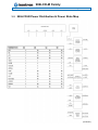
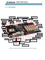
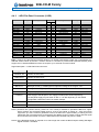
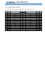
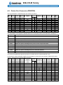
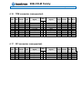
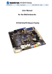
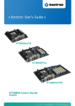
1
986LCD-M Family KTD-N0837-B Public User Manual Date: 2012-04-17 Page 1 of 91 User Manual for the Motherboards: 986LCD-M/mITX 986LCD-M/mITX BGA 986LCD-M/Flex 986LCD-M/ATXE 986LCD-M/ATXP 986LCD-M Family KTD-N0837-B Public User Manual Date: 2012-04-17 Page 2 of 91 Document revision history. Revision Date By th MLA th MLA B Apr. 17 2012 A Jan. 10 2012 Comment Added information that 986LCD-M/mITX having CF socket no longer support PCIe x16 slot. KTD-00691-Z is now replaced by KTD-N0837-A. Update UL info for ATXP version. Added BIOS setting: Staggered Spinup delay Copyright Notice: Copyright 2006, KONTRON Technology A/S, ALL RIGHTS RESERVED. No part of this document may be reproduced or transmitted in any form or by any means, electronically or mechanically, for any purpose, without the express written permission of KONTRON Technology A/S. Trademark Acknowledgement: Brand and product names are trademarks or registered trademarks of their respective owners. Disclaimer: KONTRON Technology A/S reserves the right to make changes, without notice, to any product, including circuits and/or software described or contained in this manual in order to improve design and/or performance. Specifications listed in this manual are subject to change without notice. KONTRON Technology assumes no responsibility or liability for the use of the described product(s), conveys no license or title under any patent, copyright, or mask work rights to these products, and makes no representations or warranties that these products are free from patent, copyright, or mask work right infringement, unless otherwise specified. Applications that are described in this manual are for illustration purposes only. KONTRON Technology A/S makes no representation or warranty that such application will be suitable for the specified use without further testing or modification. 986LCD-M Family KTD-N0837-B Public User Manual Date: 2012-04-17 Page 3 of 91 Life Support Policy KONTRON Technology’s PRODUCTS ARE NOT FOR USE AS CRITICAL COMPONENTS IN LIFE SUPPORT DEVICES OR SYSTEMS WITHOUT EXPRESS WRITTEN APPROVAL OF THE GENERAL MANAGER OF KONTRON Technology A/S. As used herein: 1. Life support devices or systems are devices or systems which, (a) are intended for surgical implant into body, or (b) support or sustain life and whose failure to perform, when properly used in accordance with instructions for use provided in the labeling, can be reasonably expected to result in significant injury to the user. 2. A critical component is any component of a life support device or system whose failure to perform can be reasonably expected to cause the failure of the life support device or system, or to affect its safety or effectiveness. KONTRON Technology Technical Support and Services If you have questions about installing or using your KONTRON Technology Product, check this User’s Manual first – you will find answers to most questions here. To obtain support, please contact your local Distributor or Field Application Engineer (FAE). Before Contacting Support: Please be prepared to provide as much information as possible: CPU Board 1. Type. 2. Part-number. 3. Serial Number. Configuration 1. CPU Type, Clock speed. 2. DRAM Type and Size. 3. BIOS Revision (Find the Version Info in the BIOS Setup). 4. BIOS Settings different than Default Settings (Refer to the BIOS Setup Section). System 1. O/S Make and Version. 2. Driver Version numbers (Graphics, Network, and Audio). 3. Attached Hardware: Harddisks, CD-rom, LCD Panels etc. 986LCD-M Family KTD-N0837-B Public User Manual Date: 2012-04-17 Page 4 of 91 Table of contents: 1. INTRODUCTION ......................................................................................................................................... 7 2. INSTALLATION PROCEDURE .................................................................................................................. 8 3. 4. 2.1 Installing the board ............................................................................................................................ 8 2.2 Requirement according to EN60950................................................................................................. 9 SYSTEM SPECIFICATION ....................................................................................................................... 10 3.1 Component main data ..................................................................................................................... 10 3.2 Processor support table. ................................................................................................................. 13 3.3 System Memory support ................................................................................................................. 14 3.4 System overview .............................................................................................................................. 14 3.5 986LCD-M Power Distribution & Power State Map ....................................................................... 15 3.6 Power Consumption ........................................................................................................................ 17 3.7 986LCD-M Clock Distribution ......................................................................................................... 20 CONNECTOR DEFINITIONS ................................................................................................................... 21 4.1 Connector layout .............................................................................................................................. 22 4.1.1 986LCD-M/mITX ......................................................................................................................... 22 4.1.2 986LCD-M/mITX BGA ................................................................................................................ 23 4.1.3 986LCD-M/Flex ........................................................................................................................... 24 4.1.4 986LCD-M/ATXP ........................................................................................................................ 25 4.1.5 986LCD-M/ATXE ........................................................................................................................ 26 4.2 Power Connector (ATXPWR) .......................................................................................................... 27 4.3 Keyboard and PS/2 mouse connectors ......................................................................................... 28 4.3.1 Stacked MINI-DIN keyboard and mouse Connector (MSE & KBD) ............................................ 28 4.3.2 Keyboard and mouse pin-row Connector (KBDMSE) ................................................................. 28 4.4 Display Connectors ......................................................................................................................... 29 4.4.1 CRT Connector (CRT) ................................................................................................................ 29 4.4.2 TV-Out (Optional)........................................................................................................................ 30 4.4.3 LVDS Flat Panel Connector (LVDS) ........................................................................................... 31 4.5 PCI-Express Connectors ................................................................................................................. 32 4.5.1 PCI-Express x16/ SDVO connector ............................................................................................ 32 4.5.2 PCI-Express x4 in a x16 connector ........................................................................................... 33 4.5.3 miniPCI-Express connector ........................................................................................................ 35 4.6 Parallel ATA harddisk interface ...................................................................................................... 36 4.6.1 IDE Hard Disk Connector (IDE_P) .............................................................................................. 37 4.6.2 CF Connector (CF) ..................................................................................................................... 38 4.7 Serial ATA harddisk interface ......................................................................................................... 39 4.7.1 SATA Hard Disk Connector (SATA0, SATA1, SATA2, SATA3) ................................................. 39 4.8 Printer Port Connector (PRINTER). ................................................................................................ 40 986LCD-M Family KTD-N0837-B Public User Manual Date: 2012-04-17 Page 5 of 91 Serial Ports ....................................................................................................................................... 41 4.9 4.9.1 Com1 (Port1) DB9 Connector. .................................................................................................... 41 4.9.2 Com2, Com3 & Com4 Pin Header Connectors. ......................................................................... 41 4.10 Ethernet connectors..................................................................................................................... 42 4.10.1 Ethernet connector 1 (ETHER1) ................................................................................................. 42 4.10.2 Ethernet connector 2/3 (ETHER2/3) ........................................................................................... 43 4.11 Firewire/ IEEE-1394 connectors. ................................................................................................. 44 4.11.1 IEEE1394 Connector (IEEE1394_0) ........................................................................................... 44 4.11.2 IEEE1394 Connector (IEEE1394_1) ........................................................................................... 44 4.12 USB Connector (USB) .................................................................................................................. 45 4.12.1 USB Connector 0/2 (USB0/2) ..................................................................................................... 45 4.12.2 USB Connector 4/5 (USB4/5) ..................................................................................................... 46 4.12.3 USB Connector 6/7 (USB6_7) .................................................................................................... 46 4.13 Audio Connector .......................................................................................................................... 47 4.13.1 Audio Line-in, Line-out and Microphone ..................................................................................... 47 4.13.2 CD-ROM Audio input (CDROM) ................................................................................................. 48 4.13.3 AUDIO Header (AUDIO_HEAD) ................................................................................................. 49 4.14 Fan connectors , FAN_CPU and FAN_SYS. ............................................................................... 50 4.15 The Clear CMOS Jumper, Clr-CMOS. ......................................................................................... 50 4.16 TPM connector (unsupported). ................................................................................................... 51 4.17 SPI connector (unsupported). ..................................................................................................... 51 4.18 Front Panel connector (FRONTPNL). ......................................................................................... 52 4.19 Feature Connector (FEATURE) ................................................................................................... 53 4.20 PCI Slot .......................................................................................................................................... 54 4.20.1 PCI Slot Connector .................................................................................................................... 54 Signal Description –PCI Slot Connector .................................................................................................... 55 4.20.2 PCI IRQ & INT routing ................................................................................................................ 57 5. ONBOARD CONNECTORS ..................................................................................................................... 58 6. SYSTEM RESSOURCES ......................................................................................................................... 59 7. 6.1 Memory map ..................................................................................................................................... 59 6.2 PCI devices ....................................................................................................................................... 60 6.3 Interrupt Usage ................................................................................................................................. 61 6.4 I/O Map .............................................................................................................................................. 62 6.5 DMA Channel Usage ........................................................................................................................ 63 OVERVIEW OF BIOS FEATURES ........................................................................................................... 64 7.1 System Management BIOS (SMBIOS / DMI) .................................................................................. 64 7.2 Legacy USB Support ....................................................................................................................... 64 986LCD-M Family KTD-N0837-B Public User Manual Date: 2012-04-17 Page 6 of 91 BIOS CONFIGURATION / SETUP ........................................................................................................... 65 8. 8.1 Introduction ...................................................................................................................................... 65 8.2 Main Menu......................................................................................................................................... 65 8.3 Advanced Menu ................................................................................................................................ 66 8.3.1 Advanced settings – CPU Configuration..................................................................................... 67 8.3.2 Advanced settings – IDE Configuration ...................................................................................... 68 8.3.3 Advanced settings – LAN Configuration ..................................................................................... 70 8.3.4 FW/IEEE 1394 Configuration ...................................................................................................... 71 8.3.5 Advanced settings – Super IO Configuration .............................................................................. 72 8.3.6 Advanced settings – Hardware Health Configuration ................................................................. 73 8.3.7 Advanced settings – Voltage Monitor ......................................................................................... 74 8.3.8 Advanced settings – ACPI Configuration .................................................................................... 74 8.3.9 Advanced settings – APM Configuration .................................................................................... 75 8.3.10 PCI Express Configuration.......................................................................................................... 76 8.3.11 Advanced settings – Remote Access Configuration ................................................................... 77 8.3.12 Advanced settings – USB Configuration ..................................................................................... 78 8.3.13 Advanced settings – USB Mass Storage Device Configuration.................................................. 79 8.4 PCIPnP Menu .................................................................................................................................... 80 8.5 Boot Menu......................................................................................................................................... 81 8.5.1 Boot – Boot Settings Configuration ............................................................................................. 81 8.5.2 Boot – Boot Device Priority ......................................................................................................... 83 8.6 Security Menu ................................................................................................................................... 84 8.7 Chipset Menu.................................................................................................................................... 86 8.7.1 Advanced Chipset Settings – North Bridge Chipset Configuration ............................................. 86 8.7.2 Advanced Chipset Settings – Video Function Configuration ...................................................... 87 8.7.3 Advanced Chipset Settings – SouthBridge Configuration ........................................................... 88 8.8 Exit Menu .......................................................................................................................................... 89 8.9 AMI BIOS Beep Codes ..................................................................................................................... 90 9. 10. OS SETUP ................................................................................................................................................ 91 WARRANTY .......................................................................................................................................... 91 986LCD-M Family KTD-N0837-B 1. Public User Manual Date: 2012-04-17 Page 7 of 91 Introduction This manual describes the 986LCD-M/Flex, 986LCD-M/ATXP, 986LCD-M/ATXE and 986LCD-M/mITX boards made by KONTRON Technology A/S. The boards will also be denoted 986LCD family if no differentiation is required. All boards are to be used with the Intel® Core™Duo, Intel® Core™ 2 Duo, Intel® Core™Solo and Celeron® M Processors. These belong to the Intel Yonah and Merom processor families. Use of this manual implies a basic knowledge of PC-AT hard- and software. This manual is focused on describing the 986LCD Board’s special features and is not intended to be a standard PC-AT textbook. New users are recommended to study the short installation procedure stated in chapter 3 before switching-on the power. All configuration and setup of the CPU board is either done automatically or by the user in the CMOS setup menus. Except for the CMOS Clear jumper, no jumper configuration is required. 986LCD-M Family KTD-N0837-B Public User Manual 2. Installation procedure 2.1 Installing the board Date: 2012-04-17 Page 8 of 91 To get the board running, follow these steps. In some cases the board shipped from KONTRON Technology has CPU, DDR DRAM and Cooler mounted. In this case Step 2-4 can be skipped. 1. Turn off the power supply. ! Warning: Turn off PSU (Power Supply Unit) completely (no mains power connected to the PSU) or leave the Power Connectors unconnected while configuring the board. Otherwise components (RAM, LAN cards etc.) might get damaged. Do not use PSU without 3.3V monitoring watchdog, which is standard feature in ATX PSU. Running the board without 3.3V connected will damage the board after a few minutes. 2. Insert the DDR2 DIMM 240pin DRAM module(s). Important: If only one module is used then use Slot 0. Be careful to push it in the slot(s) before locking the tabs. For a list of approved DDR2 DIMM modules contact your Distributor or FAE (list under preparation). DDR2-667 (PC5400) are supported. 3. Install the processor. The CPU is keyed and will only mount in the CPU socket in one way. Use the handle to open/ close the CPU socket. Intel® Core™Duo, Intel® Core™ 2 Duo, Intel® Core™Solo and Celeron® M Processors are supported, refer to supported processor overview for details. 4. Use heat paste or adhesive pads between CPU and cooler and connect the Fan electrically to the FAN_CPU (J21) connector. 5. Insert all external cables for hard disk, keyboard etc. except for flat panel. A CRT monitor must be connected in order to change CMOS settings to flat panel support. To achieve UDMA-66/100 performance on the IDE interface, 80poled UDMA cables must be used. When using bootable SATA disk, then connect to SATA0 or SATA2 or select in BIOS “ATA/IDE Configuration” = Enhanced. 6. Connect power supply to the board by the ATX/ BTXPWR and 4-pin ATX connectors. For board to operate connection of both the ATX/BTX and 4-pin ATX (12V) connectors are required. 7. Turn on the power on the ATX/ BTX power supply. 8. The PWRBTN_IN must be toggled to start the Power supply; this is done by shorting pins 16 (PWRBTN_IN) and pin 18 (GND) on the FRONTPNL connector (see Connector description). A “normally open” switch can be connected via the FRONTPNL connector. 9. Enter the BIOS setup by pressing the “DEL” key during boot up. Refer to the Software Manual (under preparation) for details on BIOS setup. Enter Advanced Menu / CPU Configuration / Intel SpeedStep Tech. and select “Maximum Performance”. Note: To clear all CMOS settings, including Password protection, move the CMOS_CLR jumper (with or without power) for approximately 1 minute. Alternatively turn off power and remove the battery for 1 minute, but be careful to orientate the battery corretly when reinserted. 10. Mounting the board to chassis ! Warning: When mounting the board to chassis etc. please notice that the board contains components on both sides of the PCB which can easily be damaged if board is handled without reasonable care. A damaged component can result in malfunction or no function at all. When fixing the Motherboard on a chassis it is recommended using screws with integrated washer and having diameter of ~7mm. Note: Do not use washers with teeth, as they can damage the PCB mounting hole and may cause short circuits. 986LCD-M Family KTD-N0837-B 2.2 Public User Manual Date: 2012-04-17 Page 9 of 91 Requirement according to EN60950 Users of 986LCD boards should take care when designing chassis interface connectors in order to fulfill the EN60950 standard: When an interface/connector has a VCC (or other power) pin, which is directly connected to a power plane like the VCC plane: To protect the external power lines of peripheral devices the customer has to take care about: • That the wires have the right diameter to withstand the maximum available power. • That the enclosure of the peripheral device fulfils the fire protecting requirements of IEC/EN 60950. Lithium Battery precautions: CAUTION! Danger of explosion if battery is incorrectly replaced. Replace only with same or equivalent type recommended by manufacturer. Dispose of used batteries according to the manufacturer’s instructions. VORSICHT! Explosionsgefahr bei unsachgemäßem Austausch der Batterie. Ersatz nur durch den selben oder einen vom Hersteller empfohlenen gleichwertigen Typ. Entsorgung gebrauchter Batterien nach Angaben des Herstellers. ADVARSEL! ADVARSEL Lithiumbatteri – Eksplosionsfare ved fejlagtig håndtering. Udskiftning må kun ske med batteri af samme fabrikat og type. Levér det brugte batteri tilbage til leverandøren. Eksplosjonsfare ved feilaktig skifte av batteri. Benytt samme batteritype eller en tilsvarende type anbefalt av apparatfabrikanten. Brukte batterier kasseres i henhold til fabrikantens instruksjoner. VARNING Explosionsfara vid felaktigt batteribyte. Använd samma batterityp eller en ekvivalent typ som rekommenderas av apparattillverkaren. Kassera använt batteri enligt fabrikantens instruktion. VAROITUS Paristo voi räjähtää, jos se on virheellisesti asennettu. Vaihda paristo ainoastaan laltevalmistajan suosittelemaan tyyppiin. Hävitä käytetty paristo valmistajan ohjeiden mukaisesti. 986LCD-M Family KTD-N0837-B 3. Public User Manual Date: 2012-04-17 Page 10 of 91 System specification 3.1 Component main data The table below summarises the features of the 986LCD-M/mITX, 986LCD-M/Flex, 986LCD-M/ATXP and 986LCD-M/ATXE embedded motherboards. Form factor Processor Memory Chipset Video Audio 986LCD-M/mITX: mini ITX (170.18millimeters by 170.18millimeters) 986LCD-M/Flex: Flex-ATX (190,50millimeters by 228,60millimeters) 986LCD-M/ATXP: ATX (190,50millimeters by 304,00millimeters) 986LCD-M/ATXE: ATX (190,50millimeters by 304,00millimeters) • Support for Intel® Core™Duo, Intel® Core™ 2 Duo, Intel® Core™Solo and Celeron® M Processors in 478pin Micro-FCPGA package with up to 667MHz system bus and 1/2/4MB internal cache. • Yonah (65 nanometer) and Merom (65 nanometer) family processors. • 2 pcs DDR2 DIMM 240pin DRAM sockets. • Support for DDR 400/533/667 (PC3200/PC4200/PC5300) • Support system memory from 256MB up to 3GB (2+1GB type Samsung PC5300UM378T5663AZ3-CE6 + PC5300U_M378T2953CZ3-CE6). • ECC not supported Intel 945GM Chipset consisting of: • Intel® 82945G Graphics and Memory Controller Hub (GMCH) • Intel® ICH7R I/O Controller Hub (ICH7R) • 8 Mbit Firmware Hub (FWH) • Intel® Integrated Graphics Engine (Generation 3.5) • Intel® Graphics Media Accellerator 950 (Intel® GMA 950) • Dynamic Video Memory Technology (DVMT) 3.0, 160MB/224MB when using SDRAM 256MB/512MB min. (System memory is allocated when it is needed dynamically). • Analog Display Support CRT, 400-MHz integrated RAMDAC with support for analogue monitors up to 2048x1536 at 75 Hz • Single or dual channel 18bit LVDS panel support (OpenLDI/ SPWG) up to UXGA (1600x1200) panel resolution. Interlaced Display output support. NOTE: Support of 24bit OpenLDI/ SPWG panels are not officially supported by Intel®, but is supported by the 986LCD series boards by Kontron. Kontron intends to continue to provide 24bit OpenLDI/ SPWG panel support even if Intel® withdraws this from the chipset. • TV-Out option, NTSC/ PAL, three integrated 10-bit DACs, Macrovision support. IMPORTANT: If the TV-Out option is available then you must make agreement with Macrovision (http://www.macrovision.com/) about lincence fee. Only Macrovision (not Kontron) can determine the actual licence fee which depends on the application. • Serial Digital Video Out (SDVO) ports (2 channels) for additional CRT, LVDS panel, DVI, TV-Out and/or HDMI support via Advanced Digital Display 2 (ADD2) cards or Media Expansion Cards. Dual independent pipe support, Mirror and Dual independent display support. Dual Monitor support with combinations of LVDS interface, SDVO port, CRT and TV-Out. Audio, 7.1 and 7.2 Channel High Definition Audio Codec using the Realtek ALC882 codec • Line-out • Line-in • Surround output: SIDE, LFE, CEN, BACK and FRONT • Microphone: MIC1 • CDROM in • SPDIF Interface Onboard speaker (continues) 986LCD-M Family KTD-N0837-B I/O Control Peripheral interfaces LAN Support BIOS Expansion Capabilities Hardware Monitor Subsystem Public User Manual Date: 2012-04-17 Page 11 of 91 Winbond W83627THF LPC Bus I/O Controller • Four USB 2.0 ports on I/O area • Four USB 2.0 ports on internal pinrows • One IEEE1394a Firewire port on I/O area (IEEE1394a-2000 OHCI controller) • One IEEE1394a Firewire port on internal pinrow (IEEE1394a-2000 OHCI controller) • Four Serial ports (RS232) • One Parallel port, SPP/EPP/ECP • Four Serial ATA 300 IDE interfaces • Two Parallel ATA IDE interfaces with UDMA 33, ATA-66/100 support • CF (only 986LCD-M/mITX PN 810200 and PN 810203). • PS/2 keyboard and mouse ports • 986LCD-M/mITX: 3x 10/100/1000Mbits/s LAN using Realtek RTL8111B controllers • 986LCD-M/Flex: 2x 10/100/1000Mbits/s LAN using Realtek RTL8111B controllers • 986LCD-M/ATXP: 3x 10/100/1000Mbits/s LAN using Realtek RTL8111B controllers • 986LCD-M/ATXE: 2x 10/100/1000Mbits/s LAN using Realtek RTL8111B controllers • PXE netboot supported. Wake On LAN (WOL) supported. • Kontron Technology / AMI BIOS (core version) • Support for Advanced Configuration and Power Interface (ACPI 3.0), Plug and Play o Suspend To Ram o Suspend To Disk o Intel Speed Step • Secure CMOS/ OEM Setup Defaults • “Always On” BIOS power setting • RAID Support (RAID modes 0, 1, 5 and 10) (for Linux O/S only RAID 0 and 1) • PCI Bus routed to PCI slot(s) (PCI Local Bus Specification Revision 2.3) o 986LCD-M/mITX: 1 slot PCI 2.3, 32 bits, 33 MHz, 5V compliant o 986LCD-M/Flex: 2 slots PCI 2.3, 32 bits, 33 MHz, 5V compliant o 986LCD-M/ATXP: 6 slots PCI 2.3, 32 bits, 33 MHz, 5V compliant o 986LCD-M/ATXE: 5 slots PCI 2.3, 32 bits, 33 MHz, 5V compliant • PCI-Express bus routed to PCI Express slot(s) (PCI Express 1.0a) o 986LCD-M/mITX: 1 slot PCI-Express x16 (except PN 810200-45xx-R18 and PN 810203-45xx-R18 and later versions). o 986LCD-M/Flex: 1 slot PCI-Express x16, 1 slot PCI-Express x4 o 986LCD-M/ATXP: 1 slot PCI-Express x16 o 986LCD-M/ATXE: 1 slot PCI-Express x16, 1 slot PCI-Express x4 • Mini PCI-Express routed to mini PCI-Express connector Support for Mini PCI-Express modules with no components on backside. o 986LCD-M/mITX: 1 slot mini PCI-Express x1 o 986LCD-M/Flex: None o 986LCD-M/ATXP: 1 slot mini PCI-Express x1 o 986LCD-M/ATXE: None • SMBus routed to FEATURE, PCI slot, PCI Express and mini-PCI Express connectors • LPC Bus routed to TPM connector • DDC Bus routed to LVDS and CRT connector • 8 x GPIOs (General Purpose I/Os) routed to FEATURE connector • Smart Fan control system, support Thermal® and Speed® cruise for three onboard Fan control connectors: FAN_CPU, FAN_SYS and FEATURE • Three thermal inputs: CPU die temperature, System temperature and External temperature input routed to FEATURE connector. (Precision +/- 7ºC) • Voltage monitoring • Intrusion detect input SMI violations (BIOS) on HW monitor not supported. Supported by API (Windows). (continues) 986LCD-M Family KTD-N0837-B Operating Systems Support Environmental Conditions Public User Manual Date: 2012-04-17 Page 12 of 91 • Win2000 • WinXP • Win2003 • WinXP Embedded • WinCE.net (limitations may apply) • Linux: Feodora Core 5, Suse 10.01 (limitations may apply) Operating: 0°C – 60°C operating temperature (forced cooling). It is the customer’s responsibility to provide sufficient airflow around each of the components to keep them within allowed temperature range. 10% - 90% relative humidity (non-condensing) Storage: -20°C – 70°C 5% - 95% relative humidity (non-condensing) Electro Static Discharge (ESD) / Radiated Emissions (EMI): All Peripheral interfaces intended for connection to external equipment are ESD/ EMI protected. EN 61000-4-2:2000 ESD Immunity EN55022:1998 class B Generic Emission Standard. Safety: UL 60950-1:2003, First Edition CSA C22.2 No. 60950-1-03 1st Ed. April 1, 2003 Product Category: Information Technology Equipment Including Electrical Business Equipment Product Category CCN: NWGQ2, NWGQ8 File number: E194252 Theoretical MTBF: 160.000/91.000 hours @ 40/60ºCCalculation based on Telcordia SR-332 method. Restriction of Hazardeous Substances (RoHS): All boards in the 986LCD-M family are RoHS compliant. Battery Capacitor utilization: No Tantal capacitors used. Only Japanese brand Aluminium capacitors rated for 100ºC is used. Exchangeable 3.0V Lithium battery for onboard Real Time Clock and CMOS RAM. Manufacturer Panasonic / PN CR2032NL/LE, CR-2032L/BE or CR-2032L/BN. Expected minimum 5 years retention varies depending on temperature, actual application on/off rate and variation within chipset and other components. Approximately current draw is 2.2µA (no PSU connected). CAUTION: Danger of explosion if the battery is incorrectly replaced. Replace only with the same or equivalent type recommended by the manufacturer. Dispose of used batteries according to the manufacturer’s instructions. 986LCD-M Family KTD-N0837-B 3.2 Public User Manual Date: 2012-04-17 Page 13 of 91 Processor support table. The 986LCD-M/mITX, /Flex, /ATXP and /ATXE are designed to support the PGA (478 pins) processors: Intel® Core™ 2 Duo Mobile Processor, Merom 65 nm process, FSB 667MHz with 4 MB L2 cache Intel® Core™ Duo Processor, Yonah 65 nm process, FSB 667MHz with 2 MB L2 cache Intel® Core™ Solo Processor, Yonah 65 nm process, FSB 667MHz with 2 MB L2 cache Celeron® M Processor, Yonah 65 nm process, FSB 533MHz with 1 MB L2 cache Processor Brand Intel® Core™ 2 Duo, 65nm, 4 MB L2 Intel® Core™ Duo, 65nm, 2 MB L2 Intel® Core™ Solo, 65nm, 2 MB L2 Celeron® M, 65nm, 1 MB L2 986LCD-M/mITX(BGA) w Core Duo 986LCD-M/mITX(BGA) w Celeron M 1MB L2 Clock Speed Processor Number sSpec no. Thermal Guideline Embedded 2.33 GHz T7600 SL9SD 34.0 W No 2.16 GHz T7400 SL9SE 34.0 W Yes 2.16 GHz T7400 SLGFJ 34.0 W Yes 2.00 GHz T7200 SL9SF 34.0 W No 1.83 GHz T5600 SL9SG 34.0 W No 1.66 GHz T5500 SL9SH 34.0 W No 2.16 GHz T2600 SL8VN 31.0 W No 2.00 GHz T2500 SL8VP 31.0 W Yes 1.83 GHz T2400 SL8VQ 31.0 W No 1.66 GHz T2300 SL8VR 31.0 W No 1.83 GHz T1400 SL92V 27.0 W No 1.66 GHz T1300 SL8VY 27.0 W No 1.86 GHz 440 SL9KW 27.0W Yes 1.73 GHz 530 SL9VA 27.0 W No 1.73 GHz 530 SLA2G* 27.0 W No 1.73 GHz 430 SL92F 27.0 W No 1.60 GHz 420 SL8VZ 27.0W No 1.46 GHz 410 SL8W2 27.0 W No 1.66 GHz L2400 SL8VW 15W Yes 1.06 GHz - - 5.5W - *) For the SLA2G and in general only socket M version is supported. 986LCD-M Family KTD-N0837-B 3.3 Public User Manual Date: 2012-04-17 Page 14 of 91 System Memory support The 986LCD-M boards have two onboard DDR2 DIMM sockets and support the following memory features: • • • • • • 1.8V (only) 240-pin DDR2 SDRAM DIMMs with gold-plated contacts Supports Single- / Dual channel DDR2 SDRAM Supports 256 Mbit, 512 Mbit and 1 Gbit technologies for x8 ans x16 width devices 256MB, 512MB and 1GB Single Rank Modules supported 512MB, 1GB and 2GB Dual Rank Modules supported Maximum of 3 Gbytes (2GB + 1GB) based on Samsung PC5300U-M378T5663AZ3-CE6 + PC5300U_M378T2953CZ3-CE6). Supports 400 MHz (PC3200) , 533 MHz (PC4200), and 667 MHz (PC5400) DDR2 devices 64-bit data interface (ECC not supported) The installed DDR2 SDRAM should support the Serial Presence Detect (SPD) data structure. This allows the BIOS to read and configure the memory controller for optimal performance. If non-SPD memory is used, the BIOS will attempt to configure the memory settings, but performance and reliability may be impacted. Important: If only one module is used then use Slot 0. 3.4 System overview The block diagram below shows the architecture and main components of the 986LCD boards. The two key ® ® components on the board are the Intel 945GM and Intel ICH7R Embedded Chipsets. Components shown shaded are optional depending on board type (986LCD-M/mITX, /Flex, /ATXP or /ATXE) and variants of the board. 986LCD-M Family KTD-N0837-B 3.5 Public User Manual Date: 2012-04-17 Page 15 of 91 986LCD-M Power Distribution & Power State Map (continues) 986LCD-M Family KTD-N0837-B Public User Manual Date: 2012-04-17 Page 16 of 91 986LCD-M Family KTD-N0837-B 3.6 Public User Manual Date: 2012-04-17 Page 17 of 91 Power Consumption In order to ensure safe operation of the board, the ATX power supply must monitor the supply voltage and shut down if the supplies are out of range – refer to the hardware manual for actual power specification. The 986LCD-M board is powered through the ATX connector and the additional 12V separate supply for CPU as specified in the ATX specification; besides this the power supplied to the board must be within the ATX specification. The requirements to the supply voltages are as follows: Supply Min Max Note Vcc3 3.135V 3.465V Should be ±5% for compliance with the ATX specification Vcc 4.75V 5.25V Should be ±5% for compliance with the ATX specification +12V 11.4V 12.6V Should be ±5% for compliance with the ATX specification –12V –13.2V –10.8V Should be ±10% for compliance with the ATX specification -5V -5,50V -4.5V 5VSB 4.75V –5.25V Not required for the 986LCD-M/mITX board Should be ±5% for compliance with the ATX specification Test system configuration The following items are used in the test setup: 1. 2. 3. 4. 5. 986LCD-M board equipped with CPU, RAM and 12V active cooler if required ATX PSU CRT, PS/2 keyboard & mouse and HD Tektronix TDS 7404, P6345 probes Fluke Current Probe 80i-100S AC/DC ATX supplies 986LCD-M Incl. CRT, PS/2 Kbd/Mse and HD PSU Gnd Current Probe Tektronix TDS 7404 Note: The Power consumption of CRT, Fan and HD is not included. Test results: The power consumption of the 986LCD-M Board is measured under: 1- DOS, idle, mean 2- WindowsXP, Running 3DMARK & CPU BURN, mean 3- WindowsXP, Running 3DMARK & CPU BURN, peak 4- S1, mean 5- S3, mean 6- S4, mean 7- Inrush, peak 986LCD-M Family KTD-N0837-B Public User Manual Date: 2012-04-17 Page 986LCD-M/mITX with Core Duo (T2500) & 1GB DDR2 Ram test results: Test DOS, Idle, mean Supply +12V +5V +3V3 -12V 5VSB WinXP, 3DMARK2000 & CPUBURN, mean +12V +5V +3V3 -12V 5VSB WinXP, 3DMARK2000 & CPUBURN, peak +12V +5V +3V3 -12V 5VSB S1, mean +12V +5V +3V3 -12V 5VSB S3, mean +12V +5V +3V3 -12V 5VSB S4, mean +12V +5V +3V3 +-12V 5VSB Inrush, peak +12V +5V +3V3 -12V 5VSB Current draw 0.88A 1.48A 1.22A 0.05A 0A Total 2.34A 1.73A 1.22A 0.05A 0A Total 2.67A 2.48A 1.28A 0.08A 0A Total 0.83A 1.17A 1.21A 0.03A 0A Total 0A 0A 0A 0.03A 0.64A Total 0A 0A 0A 0A 0.64A Total 5.08A 2.48A 3.52A 0.3A 2.92A Power consumption 10.56W 7.4W 4.03W 0.6W 0W 22.59W 28.08W 8.65W 4.03W 0.6W 0W 41.36W 32.04W 12.4W 4.22W 0.96W 0W 49.62W 9.96W 5.85W 3.99W 0.36W 0W 20.16W 0W 0W 0W 0.36W 3.68W 4.04W 0W 0W 0W 0W 3.2W 3.2W 18 of 91 986LCD-M Family KTD-N0837-B Public User Manual Date: 2012-04-17 Page 986LCD-M/mITX with w/1.06GHz Celeron M 512MB test results: Test DOS, Idle, mean Supply +12V +5V +3V3 -12V 5VSB WinXP, 3DMARK2000 & CPUBURN, mean +12V +5V +3V3 -12V 5VSB WinXP, 3DMARK2000 & CPUBURN, peak +12V +5V +3V3 -12V 5VSB S1, mean +12V +5V +3V3 -12V 5VSB S3, mean +12V +5V +3V3 -12V 5VSB S4, mean +12V +5V +3V3 +-12V 5VSB Inrush, peak +12V +5V +3V3 -12V 5VSB Current draw 0.36A 1.37A 1.31A 0A 0A Total 0.4A 1.47A 1.54A 0A 0A Total 0.61A 2.1A 1.64A 0A 0A Total 0.25A 1.05A 0.75A 0A 0A Total 0A 0A 0A 0A 0.18A Total 0A 0A 0A 0A 0.18A Total 1.54A 1.02A 1.2A 0.09A 3.5A Power consumption 4.32W 6.85W 4.323W 0W 0W 15.493W 4.8W 7.35W 5.08W 0W 0W 17.232W 7.32W 10.5W 5.41W 0W 0W 23.232W 3W 5.25W 2.48W 0W 0W 10.73W 0W 0W 0W 0W 0.9W 0.9W 0W 0W 0W 0W 0.9W 0.9W 19 of 91 986LCD-M Family KTD-N0837-B 3.7 Public User Manual 986LCD-M Clock Distribution Date: 2012-04-17 Page 20 of 91 986LCD-M Family KTD-N0837-B 4. Public User Manual Date: 2012-04-17 Page 21 of 91 Connector Definitions The following sections provide pin definitions and detailed description of all on-board connectors. . The connector definitions follow the following notation: Column name Description Pin Shows the pin-numbers in the connector. The graphical layout of the connector definition tables is made similar to the physical connectors. Signal The mnemonic name of the signal at the current pin. The notation “XX#” states that the signal “XX” is active low. Type AI: Analog Input. AO: Analog Output. I: Input, TTL compatible if nothing else stated. IO: Input / Output. TTL compatible if nothing else stated. IOT: Bi-directional tristate IO pin. IS: Schmitt-trigger input, TTL compatible. IOC: Input / open-collector Output, TTL compatible. NC: Pin not connected. O: Output, TTL compatible. OC: Output, open-collector or open-drain, TTL compatible. OT: Output with tri-state capability, TTL compatible. LVDS: Low Voltage Differential Signal. PWR: Power supply or ground reference pins. Ioh: Typical current in mA flowing out of an output pin through a grounded load, while the output voltage is > 2.4 V DC (if nothing else stated). Iol: Typical current in mA flowing into an output pin from a VCC connected load, while the output voltage is < 0.4 V DC (if nothing else stated). Pull U/D On-board pull-up or pull-down resistors on input pins or open-collector output pins. Note Special remarks concerning the signal. The abbreviation TBD is used for specifications which are not available yet or which are not sufficiently specified by the component vendors. 986LCD-M Family KTD-N0837-B 4.1 4.1.1 Public User Manual Date: 2012-04-17 Page 22 of 91 Connector layout 986LCD-M/mITX Mini-PCIe (backside of 986LCD-M/mITX) (Support for modules with no components mounted on backside). CF * (backside of 986LCD-M/mITX) FAN_CPU SATA3 SATA1 SATA2 SATA0 DDR2 SLOT 1 LVDS DDR2 SLOT 0 FEATURE SPI IEEE1394 1 TPM ATX/ BTXPWR PCIe x16 / SDVO * PCI SLOT ATX+12V FRONTPNL IDE_P FAN_SYS PRINTER KBDMSE AUDIO_HEAD Clr-CMOS COM3 COM4 COM2 USB6_7 CDROM IEEE1394_0 USB5 USB4 COM1 CRT System Temperature sensor (Q12) (Mounted on backside) MSE KBD ETHER1 USB2 USB0 ETHER2 ETHER3 TV-OUT (Not available) AUDIO STACK * CF is only available on some versions of 986LCD-M/mITX (PN 810200 and PN 810203). PCIe x16 is not available on the versions 810200-45xx-R18 and 810203-45xx-R18 and later revisions. 986LCD-M Family KTD-N0837-B 4.1.2 Public User Manual Date: 2012-04-17 Page 23 of 91 986LCD-M/mITX BGA Same connectors available as on the standard 986LCD-M/mITX, except that CPU socket is replaced with BGA version of CPU. (Passive cooler included). 986LCD-M Family KTD-N0837-B 4.1.3 Public User Manual Date: 2012-04-17 24 of 91 986LCD-M/Flex SATA1 SATA2 SATA0 SATA3 System Temperature sensor (Q12) USB6_7 FRONTPNL Page ATX+12V FAN_System LVDS Clr-CMOS IDE_P ATX/ BTXPWR PCIe x16 / SDVO PCIe x4 FEATURE SPI PRINTER PCI Slot 1 TPM PCI Slot 2 FAN_CPU COM2 COM4 COM3 DDR2 SLOT 0 IEEE1394_1 (Not mounted) DDR2 SLOT 1 KBDMSE AUDIO_HEAD COM1 CRT MSE KBD USB2 USB0 IEEE1394_0 USB5 USB4 CDROM Audio in ETHER2 ETHER3 AUDIO STACK ETHER1 is not available on this board TV-OUT (Not available) 986LCD-M Family KTD-N0837-B 4.1.4 Public User Manual Date: 2012-04-17 Page 25 of 91 986LCD-M/ATXP ATX/ BTXPWR System Temperature sensor (Q12) ATX+12V FAN_System Clr-CMOS PCI Slot 1 LVDS FRONTPNL Mini-PCIe (*) SATA1 SATA2 SATA0 SATA3 IDE_P FEATURE SPI USB6_7 PRINTER PCI Slot 2 - 5 TPM PCI Slot 6 FAN_CPU COM2 COM4 COM3 IEEE1394 1 DDR2 SLOT 0 PCIe x16 / SDVO DDR2 SLOT 1 KBDMSE COM1 CRT MSE KBD AUDIO HEADER ETHER1 USB2 USB0 IEEE1394_0 USB5 USB4 CDROM Audio in TV-OUT (Not available) ETHER2 ETHER3 AUDIO STACK * Support for Mini PCI-Express modules with no components mounted on backside. 986LCD-M Family KTD-N0837-B 4.1.5 Public User Manual Date: 2012-04-17 Page 26 of 91 986LCD-M/ATXE ATX/ BTXPWR System Temperature sensor (Q12) SATA1 SATA2 SATA0 SATA3 ATX+12V FRONTPNL FAN_System Clr-CMOS PCI Slot 1 LVDS IDE_P FEATURE USB6_7 SPI PRINTER PCI Slot 2 - 5 TPM PCIe x4 (in x16 socket) FAN_CPU COM2 COM4 COM3 IEEE1394 1 DDR2 SLOT 0 PCIe x16 / SDVO DDR2 SLOT 1 KBDMSE COM1 CRT MSE KBD AUDIO HEADER ETHER1 USB2 USB0 IEEE1394_0 USB5 USB4 CDROM Audio in TV-OUT (Not available) ETHER2 ETHER3 AUDIO STACK ETHER1 is not available on this board 986LCD-M Family KTD-N0837-B 4.2 Public User Manual Date: 2012-04-17 Page 27 of 91 Power Connector (ATXPWR) The 986LCD-M boards are designed to be supplied from a standard ATX or BTX power supply. ATX/ BTX Power Connector: Note Pull U/D - Ioh/Iol - PIN - - Type PWR PWR PWR PWR I PWR PWR PWR PWR PWR PWR PWR Signal 3V3 +12V +12V SB5V P_OK GND 5V GND 5V GND 3V3 3V3 12 11 10 9 8 7 6 5 4 3 2 1 24 23 22 21 20 19 18 17 16 15 14 13 Signal GND 5V 5V 5V -5V GND GND GND PSON# GND -12V 3V3 Type PWR PWR PWR PWR PWR PWR PWR PWR OC PWR PWR PWR Ioh/Iol - Pull U/D - - - Note 1 Note 1: -5V supply is not used onboard. Note 2: Use of BTX supply not required for operation, but may be required to drive high-power PCI Express x16 Add cards. ATX+12V Power Connector: Note 1 1 Pull U/D - PIN Ioh/Iol - Type PWR PWR Signal GND GND 1 2 3 4 Signal +12V +12V Type PWR PWR Ioh/Iol - Pull U/D - Note 1 1 Note 1: Use of the 4-pin ATX+12V Power Connector is required for operation of the 986LCD-M boards. See chapter “Power Consumption” regarding input tolerances on 3.3V, 5V, SB5V, +12 and -12V (also refer to ATX specification). Control signal description: Signal P_OK PS_ON# Description P_OK is a power good signal and should be asserted high by the power supply to indicate that the +5VDC and +3.3VDC outputs are above the undervoltage thresholds of the power supply. When this signal is asserted high, there should be sufficient energy stored by the converter to guarantee continuous power operation within specification. Conversely, when the output voltages fall below the undervoltage threshold, or when mains power has been removed for a time sufficiently long so that power supply operation is no longer guaranteed, P_OK should be de-asserted to a low state. The recommended electrical and timing characteristics of the P_OK (PWR_OK) signal are provided in the ATX12V Power SupplyDesign Guide. It is strongly recommended to use an ATX or BTX supply with the 986LCD-M boards, in order to implement the supervision of the 5V and 3V3 supplies. These supplies are not supervised onboard the 986LCD-M boards. Active low open drain signal from the board to the power supply to turn on the power supply outputs. Signal must be pulled high by the power supply. 986LCD-M Family KTD-N0837-B 4.3 Public User Manual Date: 2012-04-17 Page 28 of 91 Keyboard and PS/2 mouse connectors Attachment of a keyboard or PS/2 mouse adapter can be done through the stacked PS/2 mouse and keyboard connector (MSE & KBD). Both interfaces utilize open-drain signaling with on-board pull-up. The PS/2 mouse and keyboard is supplied from 5V_STB when in standby mode in order to enable keyboard or mouse activity to bring the system out from power saving states. The supply is provided through a 1.1A resetable fuse. 4.3.1 Note Stacked MINI-DIN keyboard and mouse Connector (MSE & KBD) Pull U/D Ioh/Iol Type Signal - - - NC 6 - - PWR - 5V/SB5V NC 4 - NC 6 PWR - 5V/SB5V NC 4 - PIN - 2 2 Signal Type Ioh/Iol Pull U/D 5 MSCLK IOC TBD 4K7 3 GND MSDAT PWR IOC TBD 4K7 5 KBDCLK IOC TBD 4K7 3 GND KBDDAT PWR IOC TBD 4K7 1 1 Note Signal Description – Keyboard & and mouse Connector (MSE & KBD), see below. 4.3.2 Keyboard and mouse pin-row Connector (KBDMSE) PIN 1 2 3 4 5 6 Signal KBDCLK KBDDAT MSCLK MSDAT 5V/SB5V GND Type IOC IOC IOC IOC PWR PWR Ioh/Iol TBD TBD TBD TBD - Pull U/D 4K7 4K7 4K7 4K7 - Note Signal Description – Keyboard & and mouse Connector (KBDMSE). Signal Description MSCLK Bi-directional clock signal used to strobe data/commands from/to the PS/2 mouse. MSDAT Bi-directional serial data line used to transfer data from or commands to the PS/2 mouse. KDBCLK Bi-directional clock signal used to strobe data/commands from/to the PC-AT keyboard. KBDDAT Bi-directional serial data line used to transfer data from or commands to the PC-AT keyboard. 986LCD-M Family KTD-N0837-B 4.4 Public User Manual Date: 2012-04-17 Page 29 of 91 Display Connectors The 986LCD-M board family provides onboard two basic types of interfaces to a display: Analog CRT interface and a digital interface typically used with flat panels. The digital interface to flat panels can be achieved through the onboard LVDS dual channel interface and/or the SDVO port available on the PCI Express connector. 4.4.1 CRT Connector (CRT) Note Pull U/D Ioh/Iol Type Signal PIN /75R * A0 RED 1 /75R * A0 GREEN 2 6 11 7 12 8 /75R * A0 BLUE 3 13 9 - - - NC 4 - - PWR DIG-GND 5 14 10 15 Signal Type Ioh/Iol ANA-GND NC ANA-GND DDCDAT ANA-GND HSYNC 5V VSYNC DIG-GND DDCCLK PWR PWR IO PWR O PWR O PWR IO TBD TBD TBD TBD Pull U/D Note 2K2 2K2 Note 1: The 5V supply in the CRT connector is fused by a 1.1A reset-able fuse. Signal Description - CRT Connector: Signal Description HSYNC CRT horizontal synchronization output. VSYNC CRT vertical synchronization output. DDCCLK Display Data Channel Clock. Used as clock signal to/from monitors with DDC interface. DDCDAT Display Data Channel Data. Used as data signal to/from monitors with DDC interface. RED Analog output carrying the red color signal to the CRT. For 75 Ohm cable impedance. GREEN BLUE Analog output carrying the green color signal to the CRT. For 75 Ohm cable impedance. Analog output carrying the blue color signal to the CRT. For 75 Ohm cable impedance. DIG-GND Ground reference for HSYNC and VSYNC. ANA-GND Ground reference for RED, GREEN, and BLUE. 1 986LCD-M Family KTD-N0837-B 4.4.2 Public User Manual Date: 2012-04-17 Page 30 of 91 TV-Out (Optional) Optionally the 986LCD-M board include TV-Out connector with support for Component, S-Video and Composite Output interfaces and NTSC/ PAL output format. The Intel® 945GM chipset include Macrovision support. IMPORTANT: If the TV-Out option is available then you must make agreement with Macrovision (http://www.macrovision.com/) about lincence fee. Only Macrovision (not Kontron) can determine the actual licence fee which depends on the application. Note Pull U/D PIN Ioh/Iol Type Signal Signal TVDACC GND TVDACB 4 2 6 7 3 5 1 GND GND Signal TVDACA Description TVDAC Channel A output supports: Composite: CVBS signal Component: Chrominance (Pb) analog signal TVDACB TVDAC Channel B output supports: S-Video: Luminance analog signal Component: Luminance (Y) analog signal TVDACC TVDAC Channel C output supports: S-Video: Chrominance analog signal Component: Chrominance (Pr) analog signal GND TVDACA Type Ioh/Iol Pull U/D Note 986LCD-M Family KTD-N0837-B 4.4.3 Public User Manual Date: 2012-04-17 Page 31 of 91 LVDS Flat Panel Connector (LVDS) Note Max. 0.5A Max. 0.5A Max. 0.5A Max. 0.5A Max. 0.5A 4K7Ω, 3.3V 3.3V level 3.3V level Note 1 Max. 0.5A Note 1 Max. 0.5A Type PWR PWR PWR PWR PWR OT OT OT LVDS LVDS LVDS LVDS LVDS PWR LVDS LVDS LVDS LVDS LVDS PWR Signal +12V +12V +12V +5V LCDVCC DDC CLK BKLTCTL BKLTEN# LVDS A0LVDS A1LVDS A2LVDS ACLKLVDS A3GND LVDS B0LVDS B1LVDS B2LVDS BCLKLVDS B3GND Pin 1 3 5 7 9 11 13 15 17 19 21 23 25 27 29 31 33 35 37 39 2 4 6 8 10 12 14 16 18 20 22 24 26 28 30 32 34 36 38 40 Signal +12V +12V GND GND LCDVCC DDC DATA VDD ENABLE GND LVDS A0+ LVDS A1+ LVDS A2+ LVDS ACLK+ LVDS A3+ GND LVDS B0+ LVDS B1+ LVDS B2+ LVDS BCLK+ LVDS B3+ GND Type PWR PWR PWR PWR PWR OT OT PWR LVDS LVDS LVDS LVDS LVDS PWR LVDS LVDS LVDS LVDS LVDS PWR Note Max. 0.5A Max. 0.5A Max. 0.5A Max. 0.5A Max. 0.5A 4K7Ω, 3.3V 3.3V level Max. 0.5A Note 1 Max. 0.5A Note 1 Max. 0.5A Note 1: Support of 24bit OpenLDI/ SPWG panels is not officially supported by Intel®, but is supported by the 986LCD series boards by Kontron. Kontron intends to continue to provide 24bit OpenLDI/ SPWG panel support even if Intel® withdraws this from the chipset, by an external converter module. Signal Description – LVDS Flat Panel Connector: Signal Description LVDS A0..A3 LVDS A Channel data LVDS ACLK LVDS A Channel clock LVDS B0..B3 LVDS B Channel data LVDS BCLK LVDS B Channel clock BKLTCTL Backlight control (1), PWM signal to implement voltage in the range 0-3.3V BKLTEN# Backlight Enable signal (active low) (2) VDD ENABLE LCDVCC Output Display Enable. VCC supply to the flat panel. This supply includes power-on/off sequencing. The flat panel supply may be either 5V DC or 3.3V DC depending on the CMOS configuration. Maximum load is 1A at both voltages. DDC CLK DDC Channel Clock DDC DATA DDC Channel Data Note 1) Windows API (version Hwmon_KTAPI ver 4.5 or newer) is available to operate the BKLTCTL signal. Some Inverters has a limited voltage range 0- 2.5V for this signal: If voltage is > 2.5V the Inverter might latch up. Some Inverters generates noise to the BKLTCTL signal resulting in making the lvds transmision fail (corrupted picture on the display). By adding 1K Ohm resistor in series with this signal and mounted in the Inverter end of the cable kit the noise is limited and picture is stabil. Note 2) If the Backlight Enable is required to be active high then make the BIOS Chipset setting: Backlight Signal Inversion = Enabled. 986LCD-M Family KTD-N0837-B 4.5 4.5.1 Public User Manual Date: 2012-04-17 Page 32 of 91 PCI-Express Connectors PCI-Express x16/ SDVO connector The 986LCD-M boards supports one 16-lane (x16) PCI Express port for external PCI Express based graphics boards or ADD2 devices. PCIe x16 is not available on 986LCD-M/mITX versions 810200-45xx-R18 and 810203-45xx-R18 and later revisions (because of mechanical conflict with CF socket). Note Type Signal PIN Signal +12V +12V +12V GND SMB_CLK SMB_DATA GND +3V3 NC SB3V3 WAKE# B1 B2 B3 B4 B5 B6 B7 B8 B9 B10 B11 A1 A2 A3 A4 A5 A6 A7 A8 A9 A10 A11 NC +12V +12V GND NC NC NC NC +3V3 +3V3 RST# NC GND PEG_TXP[15] / SDVOB_RED PEG_TXN[15] / SDVOB_RED# GND SDVO_CTRLCLK GND PEG_TXP[14] / SDVOB_GREEN PEG_TXN[14] / SDVOB_GREEN# GND GND PEG_TXP[13] / SDVOB_BLUE PEG_TXN[13] / SDVOB_BLUE# GND GND PEG_TXP[12] / SDVOB_CLKP PEG_TXN[12] / SDVOB_CLKN GND NC SDVO_CTRLDATA GND PEG_TXP[11] / SDVOC_RED PEG_TXN[11] / SDVOC_RED# GND GND PEG_TXP[10] / SDVOC_GREEN PEG_TXN[10] / SDVOC_GREEN# GND GND PEG_TXP[9] / SDVOC_BLUE PEG_TXN[9] / SDVOC_BLUE# GND GND PEG_TXP[8] / SDVOC_CLKN PEG_TXN[8] / SDVOC_CLKP GND PRSNT#2 GND PEG_TXP[7] PEG_TXN[7] GND GND PEG_TXP[6] PEG_TXN[6] GND GND B12 B13 B14 B15 B16 B17 B18 B19 B20 B21 B22 B23 B24 B25 B26 B27 B28 B29 B30 B31 B32 B33 B34 B35 B36 B37 B38 B39 B40 B41 B42 B43 B44 B45 B46 B47 B48 B49 B50 B51 B52 B53 B54 B55 B56 B57 A12 A13 A14 A15 A16 A17 A18 A19 A20 A21 A22 A23 A24 A25 A26 A27 A28 A29 A30 A31 A32 A33 A34 A35 A36 A37 A38 A39 A40 A41 A42 A43 A44 A45 A46 A47 A48 A49 A50 A51 A52 A53 A54 A55 A56 A57 GND PCIE_x16 CLK PCIE_x16 CLK# GND PEG_RXP[15] / SDVO_TVCLKIN PEG_RXN[15] / SDVO_TVCLKIN# GND NC GND PEG_RXP[14] / SDVOB_INT PEG_RXN[14] / SDVOB_INT# GND GND PEG_RXP[13] / SDVO_FLDSTALL PEG_RXN[13] / SDVO_FLDSTALL# GND GND PEG_RXP[12] PEG_RXN[12] GND NC NC GND PEG_RXP[11] PEG_RXN[11] GND GND PEG_RXP[10] / SDVOC_INT PEG_RXN[10] / SDVOC_INT# GND GND PEG_RXP[9] PEG_RXN[9] GND GND PEG_RXP[8] PEG_RXN[8] GND NC GND PEG_RXP[7] PEG_RXN[7] GND GND PEG_RXP[6] PEG_RXN[6] Type Note (continues) 986LCD-M Family KTD-N0837-B Public User Manual PEG_TXP[5] PEG_TXN[5] GND GND PEG_TXP[4] PEG_TXN[4] GND GND PEG_TXP[3] PEG_TXN[3] GND GND PEG_TXP[2] PEG_TXN[2] GND GND PEG_TXP[1] PEG_TXN[1] GND GND PEG_TXP[0] PEG_TXN[0] GND NC NC 4.5.2 Date: 2012-04-17 B58 B59 B60 B61 B62 B63 B64 B65 B66 B67 B68 B69 B70 B71 B72 B73 B74 B75 B76 B77 B78 B79 B80 B81 B82 A58 A59 A60 A61 A62 A63 A64 A65 A66 A67 A68 A69 A70 A71 A72 A73 A74 A75 A76 A77 A78 A79 A80 A81 A82 Page 33 of 91 GND GND PEG_RXP[5] PEG_RXN[5] GND GND PEG_RXP[4] PEG_RXN[4] GND GND PEG_RXP[3] PEG_RXN[3] GND GND PEG_RXP[2] PEG_RXN[2] GND GND PEG_RXP[1] PEG_RXN[1] GND GND PEG_RXP[0] PEG_RXN[0] GND PCI-Express x4 in a x16 connector The 986LCD-M/Flex and the 986LCD-M/ATXE boards supports one 4-lane PCI Express (x16) port. Note Type Signal PIN Signal +12V +12V +12V GND SMB_CLK SMB_DATA GND +3V3 NC SB3V3 WAKE# B1 B2 B3 B4 B5 B6 B7 B8 B9 B10 B11 A1 A2 A3 A4 A5 A6 A7 A8 A9 A10 A11 NC +12V +12V GND NC NC NC NC +3V3 +3V3 RST# NC GND PCIE_TXP[1] PCIE_TXN[1] GND NC GND PCIE_TXP[2] PCIE_TXN[2] GND GND PCIE_TXP[3] PCIE_TXN[3] GND GND PCIE_TXP[4] PCIE_TXN[4] GND NC NC GND NC NC B12 B13 B14 B15 B16 B17 B18 B19 B20 B21 B22 B23 B24 B25 B26 B27 B28 B29 B30 B31 B32 B33 B34 A12 A13 A14 A15 A16 A17 A18 A19 A20 A21 A22 A23 A24 A25 A26 A27 A28 A29 A30 A31 A32 A33 A34 GND PCIE_x4 CLK PCIE_x4 CLK# GND PCIE_RXP[1] PCIE_RXN[1] GND NC GND PCIE_RXP[2] PCIE_RXN[2] GND GND PCIE_RXP[3] PCIE_RXN[3] GND GND PCIE_RXP[4] PCIE_RXN[4] GND NC NC GND Type Note (continues) 986LCD-M Family KTD-N0837-B Public User Manual GND GND NC NC GND GND NC NC GND GND NC NC GND NC GND NC NC GND GND NC NC GND GND NC NC GND GND NC NC GND GND NC NC GND GND NC NC GND GND NC NC GND GND NC NC GND NC NC Date: 2012-04-17 B35 B36 B37 B38 B39 B40 B41 B42 B43 B44 B45 B46 B47 B48 B49 B50 B51 B52 B53 B54 B55 B56 B57 B58 B59 B60 B61 B62 B63 B64 B65 B66 B67 B68 B69 B70 B71 B72 B73 B74 B75 B76 B77 B78 B79 B80 B81 B82 A35 A36 A37 A38 A39 A40 A41 A42 A43 A44 A45 A46 A47 A48 A49 A50 A51 A52 A53 A54 A55 A56 A57 A58 A59 A60 A61 A62 A63 A64 A65 A66 A67 A68 A69 A70 A71 A72 A73 A74 A75 A76 A77 A78 A79 A80 A81 A82 NC NC GND GND NC NC GND GND NC NC GND GND NC NC GND NC GND NC NC GND GND NC NC GND GND NC NC GND GND NC NC GND GND NC NC GND GND NC NC GND GND NC NC GND GND NC NC GND Page 34 of 91 986LCD-M Family KTD-N0837-B 4.5.3 Public User Manual Date: 2012-04-17 Page 35 of 91 miniPCI-Express connector The 986LCD-M/mITX and the 986LCD-M/ATXP supports one miniPCI Express port. Note Type Signal PIN Signal WAKE# NC NC NC GND PCIE_mini CLK# PCIE_mini CLK GND 1 3 5 7 9 11 13 15 2 4 6 8 10 12 14 16 +3V3 GND +1.5V NC NC NC NC NC NC NC GND PCIE_RXN PCIE_RXP GND GND PCIE_TXN PCIE_TXP GND NC NC NC NC NC NC NC NC 17 19 21 23 25 27 29 31 33 35 37 39 41 43 45 47 49 51 18 20 22 24 26 28 30 32 34 36 38 40 42 44 46 48 50 52 GND W_Disable RST# +3V3 Dual GND +1.5V SMB_CLK SMB_DATA GND NC NC GND NC NC NC +1.5V GND +3V3 Type Note 986LCD-M Family KTD-N0837-B 4.6 Public User Manual Date: 2012-04-17 Page 36 of 91 Parallel ATA harddisk interface One parallel primary ATA harddisk controller is available on the board. Standard 3½” harddisks or CD-ROM drives may be attached to the primary controller board by means of the 40 pin IDC connectors, IDE_P. The primary controller is shared between the IDE_P connector and the backside Compact Flash connector (986LCD-M/mITX only). In case CF is utilized, only one IDE device is supported on the IDE_P connector. The harddisk controllers support Bus master IDE, ultra DMA 33/66/100 MHz and standard operation modes. The signals used for the harddisk interface are the following: Signal PDA2..0 HDCS1..0# Description Address lines, used to address the I/O registers in the IDE hard disk. Hard Disk Chip-Select. HDCS0# selects the primary hard disk. D15..8 High part of data bus. D7..0 Low part of data bus. IOR# I/O Read. IOW# I/O Write. IORDY# This signal may be driven by the hard disk to extend the current I/O cycle. RESET# Reset signal to the hard disk. The signal is similar to RSTDRV in the PC-AT bus. HDIRQ Interrupt line from hard disk. Routed by the SiS630 chipset to PC-AT bus interrupt. CBLID This input signal (CaBLe ID) is used to detect the type of attached cable: 80-wire cable when low input and 40-wire cable when 5V via 10Kohm (pull-up resistor). DDREQ Disk DMA Request might be driven by the IDE hard disk to request bus master access to the PCI bus. The signal is used in conjunction with the PCI bus master IDE function and is not associated with any PC-AT bus compatible DMA channel. DDACK# Disk DMA Acknowledge. Active low signal grants IDE bus master access to the PCI bus. HDACT# Signal from hard disk indicating hard disk activity. The signal level depends on the hard disk type, normally active low. The signals from primary and secondary controller are routed together through diodes and passed to the connector FEATURE. All of the above signals are compliant to [4]. The pinout of the connectors are defined in the following sections. 986LCD-M Family KTD-N0837-B 4.6.1 Public User Manual Date: 2012-04-17 Page 37 of 91 IDE Hard Disk Connector (IDE_P) This connector can be used for connection of two primary IDE drives. If Compact Flash connector (986LCDM/mITX only) is utilized, only one IDE device is supported. Note Pull U/D Ioh/Iol Type Signal 4K7 8K2 - TBD TBD TBD TBD TBD TBD TBD TBD TBD TBD TBD TBD TBD TBD - O IO IO IO IO IO IO IO IO PWR I O O I O I O O O I RESET# DA7 DA6 DA5 DA4 DA3 DA2 DA1 DA0 GND DDRQ IOW# IOR# IORDY DDACK# HDIRQ PDA1 PDA0 HDCS1# HDACT# PIN 1 3 5 7 9 11 13 15 17 19 21 23 25 27 29 31 33 35 37 39 2 4 6 8 10 12 14 16 18 20 22 24 26 28 30 32 34 36 38 40 Signal Type Ioh/Iol GND DA8 DA9 DA10 DA11 DA12 DA13 DA14 DA15 KEY GND GND GND GND GND NC CBLID# PDA2 HDCS3# GND PWR IO IO IO IO IO IO IO IO PWR PWR PWR PWR PWR I O O PWR TBD TBD TBD TBD TBD TBD TBD TBD TBD TBD - Pull U/D - Note 986LCD-M Family KTD-N0837-B 4.6.2 Public User Manual Date: 2012-04-17 Page 38 of 91 CF Connector (CF) This connector is mounted on the backside of the 986LCD-M/mITX only. If a Compact Flash Disk is used, only one IDE device is supported on the IDE_P connector. The CF socket support DMA/UDMA CF modules. CF is only available on some versions of 986LCD-M/mITX (PN 810200 and PN 810203). Please notice that PCIe x16 is not available on the versions 810200-45xx-R18 and 810203-45xx-R18 and later revisions. Note 2 1 Pull U/D 8K2 4K7 - Ioh/Iol TBD TBD TBD TBD TBD TBD TBD TBD TBD TBD TBD TBD - Type IO IO IO IO IO O O O PWR I PWR PWR O I I O I I IO IO IO PWR Signal NC DA11 DA12 DA13 DA14 DA15 HDCSA1# NC IORA# IOWA# 5V HDIRQA 5V GND NC RESET_C# IORDYA DDRQA DDACKA# HDACTA# CBLIDA# DB8 DB9 DB10 GND PIN 26 27 28 29 30 31 32 33 34 35 36 37 38 39 40 41 42 43 44 45 46 47 48 49 50 1 2 3 4 5 6 7 8 9 10 11 12 13 14 15 16 17 18 19 20 21 22 23 24 25 Note 1: Pin is longer than average length of the other pins. Note 2: Pin is shorter than average length of the other pins. Signal GND DB3 DB4 DB5 DB6 DB7 HDCSA0# GND GND GND GND GND 5V GND GND GND GND DAA2 DAA1 DAA0 DB0 DB1 DB2 NC NC Type PWR IO IO IO IO IO O PWR PWR PWR PWR PWR PWR PWR PWR PWR PWR O O O IO IO IO Ioh/Iol TBD TBD TBD TBD TBD TBD TBD TBD TBD Pull U/D - - - - Note 1 2 986LCD-M Family KTD-N0837-B 4.7 Public User Manual Date: 2012-04-17 Page 39 of 91 Serial ATA harddisk interface The 986LCD-M boards have an intergrated SATA Host controller that supports independent DMA operation on four ports and data transfer rates of up to 3.0Gb/s (300MB/s). The SATA controller supports AHCI mode and has integrated RAID functionality with support for RAID modes 0, 1, 5 and 10 (Linux O/S only support for RAID 0 and 1). 4.7.1 SATA Hard Disk Connector (SATA0, SATA1, SATA2, SATA3) SATA: PIN Key 1 2 3 4 5 6 7 Signal Type Ioh/Iol Pull U/D GND SATA* TX+ SATA* TXGND SATA* RXSATA* RX+ GND PWR - - PWR - - PWR - - Note The signals used for the primary Serial ATA harddisk interface are the following: Signal SATA* RX+ Description Host transmitter differential signal pair SATA* RXSATA* TX+ Host receiver differential signal pair SATA* TX“*” specifies 0, 1, 2, and 3 depending on SATA port. All of the above signals are compliant to [4]. 986LCD-M Family KTD-N0837-B 4.8 Public User Manual Date: 2012-04-17 Page 40 of 91 Printer Port Connector (PRINTER). The signal definition in standard printer port mode is as follows: Note Pull U/D Ioh/Iol Type Signal 2K2 2K2 2K2 2K2 2K2 2K2 2K2 2K2 2K2 2K2 2K2 2K2 2K2 (24)/24 24/24 24/24 24/24 24/24 24/24 24/24 24/24 24/24 - OC(O) IO IO IO IO IO IO IO IO I I I I STB# PD0 PD1 PD2 PD3 PD4 PD5 PD6 PD7 ACK# BUSY PE SLCT PIN 1 3 5 7 9 11 13 15 17 19 21 23 25 2 4 6 8 10 12 14 16 18 20 22 24 26 Signal Type Ioh/Iol Pull U/D AFD# ERR# INIT# SLIN# GND GND GND GND GND GND GND GND GND OC(O) I OC(O) OC(O) PWR PWR PWR PWR PWR PWR PWR PWR PWR (24)/24 (24)/24 (24)/24 - 2K2 2K2 2K2 2K2 - Note The interpretation of the signals in standard Centronics mode (SPP) with a printer attached is as follows: Signal Description PD7..0 Parallel data bus. The bus are able to operate in PS/2 compatible bi-directional mode. SLIN# Signal to select the printer sent from CPU board to printer. SLCT Signal from printer to indicate that the printer is selected. STB# This signal indicates to the printer that data at PD7..0 are valid. BUSY Signal from printer indicating that the printer cannot accept further data. ACK# Input indicating that the printer has received the data and is ready to accept further data. INIT# This active low output initializes (resets) the printer. AFD# This active low output causes the printer to add a line feed after each line printed. ERR# Signal from printer indicating that an error has been detected. PE# Signal from printer indicating that the printer is out of paper. The printer port additionally supports operation in the EPP and ECP mode as defined in [3]. Connecting the cable kit 821026 “Cable LPT 2mm 250mm” to the mITX or the 821031 “Cable LPT 2.54mm 250mm” implements the standard DB-25 interface: Note Pull U/D Ioh/Iol Type Signal 2K2 (24)/24 OC(O) STB# 1 2K2 24/24 IO PD0 2 2K2 24/24 IO PD1 3 2K2 24/24 IO PD2 4 2K2 24/24 IO PD3 5 2K2 24/24 IO PD4 6 2K2 24/24 IO PD5 7 2K2 24/24 IO PD6 8 2K2 24/24 IO PD7 9 2K2 - I ACK# 10 2K2 - I BUSY 11 2K2 - I PE 12 2K2 - I SLCT 13 Signal Type Ioh/Iol Pull U/D 14 AFD# OC(O) (24)/24 2K2 15 ERR# I - 2K2 16 INIT# OC(O) (24)/24 2K2 17 SLIN# OC(O) (24)/24 2K2 18 GND PWR - - 19 GND PWR - - 20 GND PWR - - 21 GND PWR - - 22 GND PWR - - 23 GND PWR - - 24 GND PWR - - 25 GND PWR - - PIN Note 986LCD-M Family KTD-N0837-B 4.9 Public User Manual Date: 2012-04-17 Page 41 of 91 Serial Ports Four RS232 serial ports are available on the 986LCD-M boards The typical interpretation of the signals in the COM ports is as follows: Signal Description TxD Transmitte Data, sends serial data to the device. The signal is set to a marking state on hardware reset when the transmitter is empty or when loop mode operation is initiated. RxD Receive Data, receives serial data from the communication link. DTR Data Terminal Ready, indicates to the device that the on-board UART is ready to establish a communication link. DSR Data Set Ready, indicates that data set is ready to establish a communication link. RTS Request To Send, indicates to the device that the on-board UART is ready to exchange data. CTS Clear To Send, indicates that the modem or data set is ready to exchange data. DCD Data Carrier Detect, indicates that the modem or data set has detected the data carrier. RI Ring Indicator, indicates that the modem has received a telephone-ringing signal. The connector pinout for each operation mode is defined in the following sections. 4.9.1 Note Com1 (Port1) DB9 Connector. Pull U/D Ioh/Iol Type Signal - - PWR GND - AO* AO* AI* AI* DTR TxD RxD DCD /5K /5K PIN 5 9 4 8 3 7 2 6 1 Signal Type Ioh/Iol RI CTS RTS DSR I AI* AO* AI* - Pull U/D Note /5K /5K /5K - * = +/-12V signals. 4.9.2 Com2, Com3 & Com4 Pin Header Connectors. The pinout of Serial ports Com2, Com3 and Com4 is as follows: Note Pull U/D Ioh/Iol Type Signal - AI* AI* AO* AO* PWR DCD RxD TxD DTR GND - - PIN 1 3 5 7 9 2 4 6 8 10 Signal Type Ioh/Iol DSR RTS CTS RI 5V AI* AO* AI* I PWR - Pull U/D Note - - * = +/-12V signals. Note 1: 5V supply is shared with supply pins in Com2/Com3/Com4 headers. The common fuse is 1.1A. If the DB9 adapter (ribbon cable) is used, the DB9 pinout will be identical to the pinout of Serial Com1. 1 986LCD-M Family KTD-N0837-B 4.10 Public User Manual Date: 2012-04-17 Page 42 of 91 Ethernet connectors. The 986LCD-M/mITX and 986LCD-M/ATXP boards supports 3 channels of 10/100/1000Mb Ethernet RTL8111B LAN controllers. The 986LCD-M/Flex and 986LCD-M/ATXE boards supports 2 channels of 10/100/1000Mb Ethernet RTL8111B LAN controllers. In order to achieve the specified performance of the Ethernet port, Category 5 twisted pair cables must be used with 10/100MB and Category 5E, 6 or 6E with 1Gb LAN networks. The signals for the Ethernet ports are as follows: Signal Description MDI[0]+ In MDI mode, this is the first pair in 1000Base-T, i.e. the BI_DA+/- pair, and is the transmit pair in 10Base-T and 100Base-TX. MDI[0]- In MDI crossover mode, this pair acts as the BI_DB+/- pair, and is the receive pair in 10Base-T and 100Base-TX. MDI[1]+ MDI[1]- In MDI mode, this is the second pair in 1000Base-T, i.e. the BI_DB+/- pair, and is the receive pair in 10Base-T and 100Base-TX. In MDI crossover mode, this pair acts as the BI_DA+/- pair, and is the transmit pair in 10Base-T and 100Base-TX. MDI[2]+ In MDI mode, this is the third pair in 1000Base-T, i.e. the BI_DC+/- pair. MDI[2]- In MDI crossover mode, this pair acts as the BI_DD+/- pair. MDI[3]+ In MDI mode, this is the fourth pair in 1000Base-T, i.e. the BI_DD+/- pair. MDI[3]- In MDI crossover mode, this pair acts as the BI_DC+/- pair. Note: MDI = Media Dependent Interface. 4.10.1 Ethernet connector 1 (ETHER1) Ethernet connector 1 is mounted together with USB Ports 0 and 2. (Not available on 986LCD-M/Flex and 986LCD-M/ATXE). The pinout of the RJ45 connector is as follows: Signal MDI0+ MDI0MDI1+ MDI2+ MDI2MDI1MDI3+ MDI3- PIN 8 7 6 5 4 Type 3 2 Ioh/Iol Note 1 On top of Ethernet1 connector there is a Green LED (to the left) turning on when a 100MHz connection is made and it is flashing when 100MHz traffic is ongoing. The Yellow LED (to the right) turns on when a 1GHz connection is made and it is flashing when traffic is ongoing. 986LCD-M Family KTD-N0837-B 4.10.2 Public User Manual Date: 2012-04-17 Page 43 of 91 Ethernet connector 2/3 (ETHER2/3) The two Ethernet channels in ETHER2/3 are supported by two discrete Ethernet controllers (RTL8111B) connected to the onboard PCI bus. The pinout of the RJ45’s connector are as follows: Signal MDI0+ MDI0MDI1+ MDI2+ MDI2MDI1MDI3+ MDI3- PIN Type 8 7 6 5 4 3 2 1 1 2 3 4 5 6 7 8 Ioh/Iol Note MDI0+ MDI0MDI1+ MDI2+ MDI2MDI1MDI3+ MDI3- Note: The connector has two LEDs which indicates connection and traffic status. Green/Yellow means 100MHz/1GHz and flasing when traffic is ongoing. The left LED is status for the ETHER3 (buttom port) and the right LED is for ETHER2. More than one type of connector is approved for this application. Please notice that it is possible that the shape of the LED might vary depending on actual type of connector. 986LCD-M Family KTD-N0837-B 4.11 Public User Manual Date: 2012-04-17 Page 44 of 91 Firewire/ IEEE-1394 connectors. The 986LCD-M boards supports two IEEE Std 1394a-2000 fully compliant cable ports at 100M bits/s, 200M bits/s, and 400M bits/s. 4.11.1 IEEE1394 Connector (IEEE1394_0) The pinout of the Firewire / IEEE1394 connector IEEE1394_0 (stacked together with USB Ports 4 and 5) is as follows: Note Pull U/D Ioh/Iol Type Signal PIN TPA0+ TPB0+ GND 10 9 1 12 11 14 13 +12V TPB0TPA0Note 1: The 12V supply for the IEEE1394_0 devices is on-board fused with a 1.5A reset-able fuse. Signal Description TPA0+ / TPA0– Differential signal pair A TPB0+ / TPB0– Differential signal pair B +12V 4.11.2 +12V supply IEEE1394 Connector (IEEE1394_1) The IEEE1394_1 is not mounted on the 986LCD-M/Flex. The pinout of the Firewire / IEEE1394 connector IEEE1394_1 is as follows: Note Pull U/D Ioh/Iol Type TPA1+ GND TPB1+ +12V KEY 1 PIN Signal 1 3 5 7 9 2 4 6 8 10 Signal Type Ioh/Iol Pull U/D TPA1GND TPB1+12V GND Note 1: The 12V supply for the IEEE1394_1 devices is on-board fused with a 1.5A reset-able fuse. Signal Description TPA1+ / TPA1– Differential signal pair A TPB1+ / TPB1– Differential signal pair B +12V +12V supply Note 1 986LCD-M Family KTD-N0837-B 4.12 Public User Manual Date: 2012-04-17 Page 45 of 91 USB Connector (USB) The 986LCD-M boards contains an Enhanced Host Controller Interface (EHCI) host controller that supports USB 2.0 allowing data transfers up to 480Mb/s. The 986LCD-M boards also contains four Universal Host Controller Interface (UHCI Revision 1.1) controllers that support USB full-speed and low-speed signaling. The 986LCD-M boards supports a total of eight USB 2.0 ports. All eight ports are high-speed, full-speed, and low-speed capable and USB Legacy mode is supported. Over-current detection on all eight USB ports is supported. USB Port 0 and 2 are supplied on the combined ETHER1, USB0, USB2 connector. USB Ports 1 and 3 are supplied on the FRONTPNL connector; please refer to the FRONTPNL connector section for the pin-out. USB Port 4 and 5 are supplied on the combined IEEE1394_0, USB4, USB5 connector. USB Port 6 and 7 are supplied on the internal USB6, USB7 pinrow. Note: It is recommended to use only High-/Full-Speed USB cable, specified in USB2.0 standard: 4.12.1 USB Connector 0/2 (USB0/2) USB Ports 0 and 2 are mounted together with ETHER1 ethernet port. Pull U/D Ioh/Iol Type Signal 1 /15K 0.25/2 PWR IO 5V/SB5V USB0- 1 /15K 0.25/2 PWR IO 5V/SB5V USB2- Note PIN 1 2 1 2 3 3 Signal Type Ioh/Iol Pull U/D GND USB0+ PWR IO 0.25/2 /15K GND USB2+ PWR IO 0.25/2 /15K Note 4 4 Note 1: The 5V supply for the USB devices is on-board fused with a 1.5A reset-able fuse. The supply is common for the two channels. SB5V is supplied during power down to allow wakeup on USB device activity. In order to meet the requirements of USB standard, the 5V input supply must be at least 5.00V. Signal Description USB0+ USB0- Differential pair works as Data/Address/Command Bus. USB2+ USB2USB5V 5V supply for external devices. Fused with 1.5A reset-able fuse. 986LCD-M Family KTD-N0837-B 4.12.2 Public User Manual Date: 2012-04-17 Page 46 of 91 USB Connector 4/5 (USB4/5) USB Ports 4 and 5 are mounted together with IEEE1394_0 port. Note Pull U/D Ioh/Iol Type Signal 1 /15K 0.25/2 PWR IO 5V/SB5V USB5- 1 /15K 0.25/2 PWR IO 5V/SB5V USB4- PIN 1 2 1 2 3 3 Signal Type Ioh/Iol Pull U/D GND USB5+ PWR IO 0.25/2 /15K GND USB4+ PWR IO 0.25/2 /15K Note 4 4 Note 1: The 5V supply for the USB devices is on-board fused with a 1.5A reset-able fuse. The supply is common for the two channels. SB5V is supplied during power down to allow wakeup on USB device activity. In order to meet the requirements of USB standard, the 5V input supply must be at least 5.00V. Signal Description USB4+ USB4- Differential pair works as Data/Address/Command Bus. USB5+ USB5USB5V 5V supply for external devices. Fused with 1.5A reset-able fuse. 4.12.3 USB Connector 6/7 (USB6_7) The pinout of the USB connector USB6_7 is as follows: Note Pull U/D 1 - Ioh/Iol Type Signal - PWR IO IO PWR 5V/SB5V USB6USB6+ GND KEY - PIN 1 3 5 7 9 2 4 6 8 10 Signal Type Ioh/Iol 5V/SB5V USB7USB7+ GND NC PWR IO IO PWR - Signal Description USB6+ USB6- Differential pair works as Data/Address/Command Bus. Pull U/D Note 1 - - USB7+ USB7USB5V 5V supply for external devices. Fused with 1.5A reset-able fuse. Note 1: The 5V supply for the USB devices is on-board fused with a 1.5A reset-able fuse. The supply is common for the two channels. SB5V is supplied during power down to allow wakeup on USB device activity. In order to meet the requirements of USB standard, the 5V input supply must be at least 5.00V. 986LCD-M Family KTD-N0837-B 4.13 Public User Manual Date: 2012-04-17 Page 47 of 91 Audio Connector 4.13.1 Audio Line-in, Line-out and Microphone Audio Line-in, Line-out and Microphone are available in the stacked audio jack connector. Below is shown audio stack configuration when configured for 8-channel audio. Note Type Signal Signal Type Note 1 1 CEN-OUT LFE-OUT GND TIP RING SLEEVE TIP RING SLEEVE LINE1-IN-L LINE1-IN-R GND IA IA PWR REAR-OUT-L REAR-OUT-R GND TIP RING SLEEVE TIP RING SLEEVE FRONT-OUT-L FRONT-OUT-R GND OA OA PWR SIDE-OUT-L SIDE-OUT-R GND TIP RING SLEEVE TIP RING SLEEVE MIC1-L MIC1-R GND IA IA PWR Note 1: Signals are shorted to GND internally in the connector, when jack-plug not inserted. Signal descriptions Signal Description Note FRONT-OUT-L Front Speakers (Speaker Out Left). FRONT-OUT-R Front Speakers (Speaker Out Right). REAR-OUT-L Rear Speakers (Surround Out Left). REAR-OUT-R Rear Speakers (Surround Out Right). SIDE-OUT-L Side speakers (Surround Out Left) SIDE-OUT-R Side speakers (Surround Out Right) CEN-OUT Center Speaker (Center Out channel). LFE-OUT Subwoofer Speaker (Low Freq. Effect Out). MIC1 LINE1-IN MIC Input 1 Line in 1 signals Audio 2, 4, 6, or 8-channel configuration Port Light Blue Lime Pink Gray Black Yellow Orange 2-channel Line in Line out Mic in - 4-channel Line in Front speaker out Mic in Rear speaker out - 6-channel Line in Front speaker out Mic in Rear speaker out Center/ Subwoofer 8-channel Line in Front speaker out Mic in Side speaker out Rear speaker out Center/ Subwoofer 1 1 986LCD-M Family KTD-N0837-B 4.13.2 Public User Manual Date: 2012-04-17 Page 48 of 91 CD-ROM Audio input (CDROM) CD-ROM audio input may be connected to this connector. It may also be used as a secondary line-in signal. PIN Signal Type Ioh/Iol 1 2 3 4 CD_Left CD_GND CD_GND CD_Right IA IA IA IA - Pull U/D - Note 1 1 Note 1: The definition of which pins are use for the Left and Right channels is not a worldwide accepted standard. Some CDROM cable kits expect reverse pin order. Signal Description CD_Left CD_Right Left and right CD audio input lines or secondary Line-in. CD_GND Analogue GND for Left and Right CD. (This analogue GND is not shorted to the general digital GND on the board). 986LCD-M Family KTD-N0837-B 4.13.3 Note Public User Manual Date: 2012-04-17 Page 49 of 91 AUDIO Header (AUDIO_HEAD) Pull U/D Ioh/ Iol - - Signal Type PWR Signal LFE-OUT AAGND FRONT-OUT-L AAGND REAR-OUT-L SIDE-OUT-L AAGND MIC1-L AAGND LINE1-IN-L NC GND SPDIF-OUT PIN 1 3 5 7 9 11 13 15 17 19 21 23 25 2 4 6 8 10 12 14 16 18 20 22 24 26 Signal CEN-OUT AAGND FRONT-OUT-R AAGND REAR-OUT-R SIDE-OUT-R AAGND MIC1-R AAGND LINE1-IN-R AAGND SPDIF-IN GND Description FRONT-OUT-L Front Speakers (Speaker Out Left). FRONT-OUT-R Front Speakers (Speaker Out Right). REAR-OUT-L Rear Speakers (Surround Out Left). REAR-OUT-R Rear Speakers (Surround Out Right). SIDE-OUT-L Side speakers (Surround Out Left) SIDE-OUT-R Side speakers (Surround Out Right) CEN-OUT Center Speaker (Center Out channel). LFE-OUT Subwoofer Speaker (Low Freq. Effect Out). NC MIC1 LINE1-IN F-SPDIF-IN F-SPDIF-OUT AAGND No connection MIC Input 1 Line in 1 signals S/PDIF Input S/PDIF Output Audio Analogue ground Note Type PWR Ioh/ Iol Pull U/D - - Note 986LCD-M Family KTD-N0837-B 4.14 Public User Manual Date: 2012-04-17 Page 50 of 91 Fan connectors , FAN_CPU and FAN_SYS. The FAN_CPU is used for connection of the active cooler for the CPU. The FAN_SYS can be used to power, control and monitor a fan for chassis ventilation etc. PIN 1 2 3 Signal SENSE 12V GND Type PWR PWR PWR Ioh/Iol - Pull U/D 4K7 - Note Signal description: Signal Description 12V +12V supply for fan, can be turned on/off or modulated (PWM) by the chipset. A maximum of 800 mA can be supplied from this pin. SENSE 4.15 Tacho signal from the fan for supervision. The signals shall be generated by an open collector transistor or similar. On board is a pull-up resistor 4K7 to +12V. The signal has to be pulses, typically 2 Hz per rotation. The Clear CMOS Jumper, Clr-CMOS. The Clr-CMOS Jumper is used to clear the CMOS content. ↑ CPU location ↑ No Jumper installed 1 3 (Pin numbers) • Jumper normal position Jumper in Clear CMOS position 2 • To clear all CMOS settings, including Password protection, move the CMOS_CLR jumper (with or without power on the system) for approximately 1 minute. Alternatively if no jumper is available, turn off power and remove the battery for 1 minute, but be careful to orientate the battery corretly when reinserted. 986LCD-M Family KTD-N0837-B 4.16 Note 4.17 Note Public User Manual Date: 2012-04-17 Page 51 of 91 TPM connector (unsupported). Pull U/D - Ioh/Iol - Type PWR PWR Signal LPC CLK LPC FRAME# LPC RST# LPC AD3 +3V3 LPC AD0 SMB_CLK SB3V3 GND SUS_STAT# PIN 1 3 5 7 9 11 13 15 17 19 2 6 8 10 12 14 16 18 20 Signal GND KEY +5V LPC AD2 LPC AD1 GND SMB_DATA LPC SERIRQ CLKRUN# LPC IRQ# Type Ioh/Iol Pull U/D Note Signal SB3V3 BOOT0 BOOT1 NC GND Type Ioh/Iol Pull U/D Note SPI connector (unsupported). Pull U/D 10K/ 10K/ 10K/ 10K/ Ioh/Iol Type Signal SPI_CLK SPI_CS SPI_ARB SPI_MOSI SPI_MISO PIN 1 3 5 7 9 2 4 6 8 10 986LCD-M Family KTD-N0837-B 4.18 Public User Manual Date: 2012-04-17 Page 52 of 91 Front Panel connector (FRONTPNL). Note Pull U/D Ioh/Iol - - - - Type PWR PWR OC PWR 1 Signal USB13_5V USB1USB1+ GND NC +5V HD_LED GND RSTIN# SB3V3 AGND MIC2-L PIN 1 3 5 7 9 11 13 15 17 19 21 23 2 4 6 8 10 12 14 16 18 20 22 24 Signal USB13_5V USB3USB3+ GND LINE2-IN-L +5V SUS_LED PWRBTN_IN# GND LINE2-IN-R AGND MIC2-R Type Ioh/Iol Pull U/D PWR PWR - - PWR - - - Note 1 Note 1: Unsupported inputs, leave these inputs unconnected. Signal USB13_5V USB1+ USB1USB3+ USB3+5V HD_LED SUS_LED PWRBTN_IN# Description +5V supply for the USB devices on USB Port 1 and 3 is on-board fused with a 1.5A reset-able fuse. The supply is common for the two channels. SB5V is supplied during power down to allow wakeup on USB device activity. Universal Serial Bus Port 1 Differentials: Bus Data/Address/Command Bus. Universal Serial Bus Port 3 Differentials: Bus Data/Address/Command Bus. Maximum load is 1A or 2A per pin if using IDC connectorfladkabel or crimp terminals respectively. Hard Disk Activity LED (active low signal). Output is via 475Ω to OC. Suspend Mode LED (active high signal). Output is via 475Ω. Power Button In. Toggle this signal low to start the ATX / BTX PSU and boot the board. RSTIN# Reset Input. Pull low to reset the board. LINE2-IN Line in 2 signals MIC2 MIC2-L and MIC2-R are unsupported. Leave these terminals unconnected. SB3V3 Standby 3.3V voltage AGND Analogue Ground for Audio 986LCD-M Family KTD-N0837-B 4.19 Public User Manual Date: 2012-04-17 Page 53 of 91 Feature Connector (FEATURE) Pull PIN Signal Signal Type Ioh/Iol U/D Note INTRUDER# 1 2 GND PWR EXT_ISAIRQ# 3 4 EXT_SMI# I PWR_OK 5 6 SB5V PWR PWR SB3V3 7 8 EXT_BAT PWR PWR +5V 9 10 GND PWR 3 2K7/ /12mA IOT GPIO0 11 12 GPIO1 IOT /12mA 2K7/ 3 3 2K7/ /12mA IOT GPIO2 13 14 GPIO3 IOT /12mA 2K7/ 3 4 2K7/ /12mA IOT GPIO4 15 16 GPIO5 IOT /12mA 2K7/ 4 4 2K7/ /12mA IOT GPIO6 17 18 GPIO7 IOT /12mA 2K7/ 4 PWR GND 19 20 FAN3OUT FAN3IN 21 22 +12V PWR TEMP3IN 23 24 VREF PWR GND 25 26 IRRX IRTX 27 28 GND PWR 1 2K7/ SMBC 29 30 SMBD 2K7/ 1 Note 1: Pull-up to +5V. Note 2: Pull-up to RTC-Voltage. Note 3: Pull-up to +5VDual (+5V or +5VSB). Note 4: Pull-up to +5VSB. Note 2 Pull U/D 243K/ Signal INTRUDER# EXT_ISAIRQ# Ioh/Iol - Type I Description INTRUDER, may be used to detect if the system case has been opened. This signal’s status is readable, so it may be used like a GPI when the Intruder switch is not needed. EXTernal ISA IRQ, (active low input) can activate standard AT-Bus IRQ-interrupt. EXT_SMI# External SMI, (active low input) signal can activate SMI interrupt. PWR_OK PoWeR OK, signal is high if no power failures is detected. SB5V StandBy +5V supply. SB3V3 Standby 3.3V. Max. load is 0.75A (1.5A < 1 sec.) (EXTernal BATtery) the + terminal of an external primary cell battery can be connected to this pin. The – terminal of the battery shall be connected to GND (etc. pin 10). The external battery is protected against charging and can be used with or without the on board battery installed. The external battery voltage shall be in the range: 2.5 - 4.0 V DC. Max. load is 0.75A (1.5A < 1 sec.) General Purpose Inputs / Output. These Signals may be controlled or monitored through the use of the KONTRON API (Application Programming Interface) available for Win98, WinXP and Win2000. FAN 3 speed control OUTput. This analogue voltage output signal can be used to control the Fan’s speed. The output has 16 values in the range from 0 – 5V. For more information please look into the datasheet for the Winbond I/O controller W83627. EXT_BAT +5V GPIO0..7 FAN3OUT FAN3IN +12V FAN3 Input. 0V to +5V amplitude Fan 3 tachometer input. VREF Max. load is 0.75A (1.5A < 1 sec.) Temperature sensor 3 input. (Recommended: Transistor 2N3904, having emitter connected to GND (pin 25), collector and basis shorted and connected to pin23 (Temp3In). Further a resistor 30K/1% shall be connected between pin 23 and pin 24 (Vref). Precision +/- 7ºC. Voltage REFerence, reference voltage to be used with TEMP3IN input. IRRX IR Receive input (IrDA 1.0, SIR up to 1.152K bps) IRTX IR Transmit output (IrDA 1.0, SIR up to 1.152K bps) SMBC SMBus Clock signal SMBD SMBus Data signal TEMP3IN 986LCD-M Family KTD-N0837-B 4.20 4.20.1 Public User Manual Date: 2012-04-17 Page 54 of 91 Note PCI Slot PCI Slot Connector Terminal Note Type Signal S C Signal Type PWR O PWR I PWR PWR I I I I OT PWR PWR O PWR O PWR I PWR IOT IOT PWR IOT IOT PWR IOT IOT PWR IOT IOT PWR IOT IOT PWR IOT PWR IOT PWR IOT IOT PWR IOC PWR IOT IOT PWR IOT IOT PWR -12V TCK GND TDO +5V +5V INTB# INTD# REQ2# REQ3# GNT2# GND GND CLKA GND CLKB GND REQ0# +5V (I/O) AD31 AD29 GND AD27 AD25 +3.3V C/BE3# AD23 GND AD21 AD19 +3.3V AD17 C/BE2# GND IRDY# +3.3V DEVSEL# GND LOCK# PERR# +3.3V SERR# +3.3V C/BE1# AD14 GND AD12 AD10 GND F01 F02 F03 F04 F05 F06 F07 F08 F09 F10 F11 F12 F13 F14 F15 F16 F17 F18 F19 F20 F21 F22 F23 F24 F25 F26 F27 F28 F29 F30 F31 F32 F33 F34 F35 F36 F37 F38 F39 F40 F41 F42 F43 F44 F45 F46 F47 F48 F49 E01 E02 E03 E04 E05 E06 E07 E08 E09 E10 E11 E12 E13 E14 E15 E16 E17 E18 E19 E20 E21 E22 E23 E24 E25 E26 E27 E28 E29 E30 E31 E32 E33 E34 E35 E36 E37 E38 E39 E40 E41 E42 E43 E44 E45 E46 E47 E48 E49 TRST# +12V TMS TDI +5V INTA# INTC# +5V CLKC +5V (I/O) CLKD GND GND GNT3# RST# +5V (I/O) GNT0# GND REQ1# AD30 +3.3V AD28 AD26 GND AD24 GNT1# +3.3V AD22 AD20 GND AD18 AD16 +3.3V FRAME# GND TRDY# GND STOP# +3.3V SDONE SB0# GND PAR AD15 +3.3V AD13 AD11 GND AD09 O PWR O O PWR I I PWR O PWR O PWR PWR OT O PWR OT PWR I IOT PWR IOT IOT PWR IOT OT PWR IOT IOT PWR IOT IOT PWR IOT PWR IOT PWR IOT PWR IO IO PWR IOT IOT PWR IOT IOT PWR IOT F52 F53 F54 F55 F56 F57 F58 F59 F60 F61 F62 E52 E53 E54 E55 F56 E57 E58 E59 E60 E61 E62 C/BE0# +3.3V AD06 AD04 GND AD02 AD00 +5V (I/O) REQ64# +5V +5V SOLDER SIDE IOT IOT PWR IOT IOT PWR IOT PWR IOT PWR PWR AD08 AD07 +3.3V AD05 AD03 GND AD01 +5V (I/O) ACK64# +5V +5V COMPONENT SIDE IOT PWR IOT IOT PWR IOT IOT PWR IOT PWR PWR 986LCD-M Family KTD-N0837-B Public User Manual Date: 2012-04-17 Page 55 of 91 Signal Description –PCI Slot Connector SYSTEM PINS Clock provides timing for all transactions on PCI and is an input to every PCI device. All other PCI signals, CLK except RST#, INTA#, INTB#, INTC#, and INTD#, are sampled on the rising edge of CLK and all other timing parameters are defined with respect to this edge. PCI operates at 33 MHz. Reset is used to bring PCI-specific registers, sequencers, and signals to a consistent state. What effect RST# RST# has on a device beyond the PCI sequencer is beyond the scope of this specification, except for reset states of required PCI configuration registers. Anytime RST# is asserted, all PCI output signals must be driven to their benign state. In general, this means they must be asynchronously tri-stated. SERR# (open drain) is floated. REQ# and GNT# must both be tri-stated (they cannot be driven low or high during reset). To prevent AD, C/BE#, and PAR signals from floating during reset, the central resource may drive these lines during reset (bus parking) but only to a logic low level–they may not be driven high. RST# may be asynchronous to CLK when asserted or deasserted. Although asynchronous, deassertion is guaranteed to be a clean, bounce-free edge. Except for configuration accesses, only devices that are required to boot the system will respond after reset. ADDRESS AND DATA Address and Data are multiplexed on the same PCI pins. A bus transaction consists of an address phase AD[31::00] followed by one or more data phases. PCI supports both read and write bursts. The address phase is the clock cycle in which FRAME# is asserted. During the address phase AD[31::00] contain a physical address (32 bits). For I/O, this is a byte address; for configuration and memory, it is a DWORD address. During data phases AD[07::00] contain the least significant byte (lsb) and AD[31::24] contain the most significant byte (msb). Write data is stable and valid when IRDY# is asserted and read data is stable and valid when TRDY# is asserted. Data is transferred during those clocks where both IRDY# and TRDY# are asserted. C/BE[3::0]# Bus Command and Byte Enables are multiplexed on the same PCI pins. During the address phase of a transaction, C/BE[3::0]# define the bus command. During the data phase C/BE[3::0]# are used as Byte Enables. The Byte Enables are valid for the entire data phase and determine which byte lanes carry meaningful data. C/BE[0]# applies to byte 0 (lsb) and C/BE[3]# applies to byte 3 (msb). Parity is even parity across AD[31::00] and C/BE[3::0]#. Parity generation is required by all PCI agents. PAR PAR is stable and valid one clock after the address phase. For data phases, PAR is stable and valid one clock after either IRDY# is asserted on a write transaction or TRDY# is asserted on a read transaction. Once PAR is valid, it remains valid until one clock after the completion of the current data phase. (PAR has the same timing as AD[31::00], but it is delayed by one clock.) The master drives PAR for address and write data phases; the target drives PAR for read data phases. INTERFACE CONTROL PINS Cycle Frame is driven by the current master to indicate the beginning and duration of an access. FRAME# FRAME# is asserted to indicate a bus transaction is beginning. While FRAME# is asserted, data transfers continue. When FRAME# is deasserted, the transaction is in the final data phase or has completed. Initiator Ready indicates the initiating agent’s (bus master’s) ability to complete the current data phase of IRDY# the transaction. IRDY# is used in conjunction with TRDY#. A data phase is completed on any clock both IRDY# and TRDY# are sampled asserted. During a write, IRDY# indicates that valid data is present on AD[31::00]. During a read, it indicates the master is prepared to accept data. Wait cycles are inserted until both IRDY# and TRDY# are asserted together. Target Ready indicates the target agent’s (selected device’s) ability to complete the current data phase of TRDY# the transaction. TRDY# is used in conjunction with IRDY#. A data phase is completed on any clock both TRDY# and IRDY# are sampled asserted. During a read, TRDY# indicates that valid data is present on AD[31::00]. During a write, it indicates the target is prepared to accept data. Wait cycles are inserted until both IRDY# and TRDY# are asserted together. Stop indicates the current target is requesting the master to stop the current transaction. STOP# LOCK# IDSEL DEVSEL# Lock indicates an atomic operation that may require multiple transactions to complete. When LOCK# is asserted, non-exclusive transactions may proceed to an address that is not currently locked. A grant to start a transaction on PCI does not guarantee control of LOCK#. Control of LOCK# is obtained under its own protocol in conjunction with GNT#. It is possible for different agents to use PCI while a single master retains ownership of LOCK#. If a device implements Executable Memory, it should also implement LOCK# and guarantee complete access exclusion in that memory. A target of an access that supports LOCK# must provide exclusion to a minimum of 16 bytes (aligned). Host bridges that have system memory behind them should implement LOCK# as a target from the PCI bus point of view and optionally as a master. Initialization Device Select is used as a chip select during configuration read and write transactions. Device Select, when actively driven, indicates the driving device has decoded its address as the target of the current access. As an input, DEVSEL# indicates whether any device on the bus has been selected. (continues) 986LCD-M Family KTD-N0837-B Public User Manual Date: 2012-04-17 Page 56 of 91 ARBITRATION PINS (BUS MASTERS ONLY) Request indicates to the arbiter that this agent desires use of the bus. This is a point to point signal. REQ# Every master has its own REQ# which must be tri-stated while RST# is asserted. Grant indicates to the agent that access to the bus has been granted. This is a point to point signal. Every GNT# master has its own GNT# which must be ignored while RST# is asserted. While RST# is asserted, the arbiter must ignore all REQ# lines since they are tri-stated and do not contain a valid request. The arbiter can only perform arbitration after RST# is deasserted. A master must ignore its GNT# while RST# is asserted. REQ# and GNT# are tri-state signals due to power sequencing requirements when 3.3V or 5.0V only add-in boards are used with add-in boards that use a universal I/O buffer. ERROR REPORTING PINS. The error reporting pins are required by all devices and maybe asserted when enabled Parity Error is only for the reporting of data parity errors during all PCI transactions except a Special PERR# Cycle. The PERR# pin is sustained tri-state and must be driven active by the agent receiving data two clocks following the data when a data parity error is detected. The minimum duration of PERR# is one clock for each data phase that a data parity error is detected. (If sequential data phases each have a data parity error, the PERR# signal will be asserted for more than a single clock.) PERR# must be driven high for one clock before being tri-stated as with all sustained tri-state signals. There are no special conditions when a data parity error may be lost or when reporting of an error may be delayed. An agent cannot report a PERR# until it has claimed the access by asserting DEVSEL# (for a target) and completed a data phase or is the master of the current transaction. System Error is for reporting address parity errors, data parity errors on the Special Cycle command, or SERR# any other system error where the result will be catastrophic. If an agent does not want a non-maskable interrupt (NMI) to be generated, a different reporting mechanism is required. SERR# is pure open drain and is actively driven for a single PCI clock by the agent reporting the error. The assertion of SERR# is synchronous to the clock and meets the setup and hold times of all bused signals. However, the restoring of SERR# to the deasserted state is accomplished by a weak pullup (same value as used for s/t/s) which is provided by the system designer and not by the signaling agent or central resource. This pull-up may take two to three clock periods to fully restore SERR#. The agent that reports SERR#s to the operating system does so anytime SERR# is sampled asserted. INTERRUPT PINS (OPTIONAL). Interrupts on PCI are optional and defined as “level sensitive,” asserted low (negative true), using open drain output drivers. The assertion and deassertion of INTx# is asynchronous to CLK. A device asserts its INTx# line when requesting attention from its device driver. Once the INTx# signal is asserted, it remains asserted until the device driver clears the pending request. When the request is cleared, the device deasserts its INTx# signal. PCI defines one interrupt line for a single function device and up to four interrupt lines for a multi-function device or connector. For a single function device, only INTA# may be used while the other three interrupt lines have no meaning. Interrupt A is used to request an interrupt. INTA# Interrupt B is used to request an interrupt and only has meaning on a multi-function device. INTB# INTC# Interrupt C is used to request an interrupt and only has meaning on a multi-function device. INTD# Interrupt D is used to request an interrupt and only has meaning on a multi-function device. 986LCD-M Family KTD-N0837-B 4.20.2 Public User Manual Date: 2012-04-17 Page 57 of 91 PCI IRQ & INT routing Board type Slot IDSEL INTA INTB INTC INTD 986LCD-M/mITX 1 AD17 INT_PIRQ#E INT_PIRQ#F INT_PIRQ#G INT_PIRQ#H 986LCD-M/FLEX 1 AD17 INT_PIRQ#E INT_PIRQ#F INT_PIRQ#G INT_PIRQ#H 2 AD18 INT_PIRQ#F INT_PIRQ#G INT_PIRQ#H INT_PIRQ#E 1 AD17 INT_PIRQ#E INT_PIRQ#F INT_PIRQ#G INT_PIRQ#H 2 AD18 INT_PIRQ#F INT_PIRQ#G INT_PIRQ#H INT_PIRQ#E 3 AD19 INT_PIRQ#G INT_PIRQ#H INT_PIRQ#E INT_PIRQ#F 4 AD20 INT_PIRQ#H INT_PIRQ#E INT_PIRQ#F INT_PIRQ#G 5 AD21 INT_PIRQ#D INT_PIRQ#C INT_PIRQ#B INT_PIRQ#A 6 AD22 INT_PIRQ#C INT_PIRQ#B INT_PIRQ#A INT_PIRQ#D 1 AD17 INT_PIRQ#E INT_PIRQ#F INT_PIRQ#G INT_PIRQ#H 2 AD18 INT_PIRQ#F INT_PIRQ#G INT_PIRQ#H INT_PIRQ#E 3 AD19 INT_PIRQ#G INT_PIRQ#H INT_PIRQ#E INT_PIRQ#F 4 AD20 INT_PIRQ#H INT_PIRQ#E INT_PIRQ#F INT_PIRQ#G 5 AD21 INT_PIRQ#D INT_PIRQ#C INT_PIRQ#B INT_PIRQ#A 986LCD-M/ATXP 986LCD-M/ATXE When using the 820982 “PCI Riser - Flex - 2slot w. arbiter” the lower slot has IDSEL / IRQs routed straight through and the top slot has the routing: IDSEL=AD22, INT_PIRQ#F, INT_PIRQ#G, INT_PIRQ#H, INT_PIRQ#E. 820982 PCI Riser shall be plugged into Slot #1. 986LCD-M Family KTD-N0837-B 5. Public User Manual Date: 2012-04-17 Page 58 of 91 Onboard Connectors Connector Onboard Connectors Mating Connectors Manufacturer Type no. Manufacturer Type no. Molex 22-23-2031 AMP 1375820-3 KBDMSE Molex 22-23-2061 Molex 22-01-2065 CDROM Foxconn HF1104E Molex 50-57-9404 Molex 70543-0038 Molex 67491-0020 Molex 67489-8005 Kontron KT 821035 (cable kit) Molex 39-01-2205 Molex 39-01-2245 FAN_SYS, FAN_CPU SATA0-3 ATXPWR Molex 44206-0002 ATX+12V Foxconn HM2502E Molex 39-01-2045 COM2 Foxconn HL20051 Molex 90635-1103 COM3 Kontron KT 821016 (cable kit) COM4 Kontron KT 821017 (cable kit) IEEE1394_0 IEEE1394_1 Foxconn HC11051-P9 Kontron KT 821040 (cable kit) USB6_7 Foxconn HC11051-P9 Kontron KT 821401 (cable kit) PRINTER for Foxconn HS55137 Molex 51110-2651 Kontron KT 821026 (cable kit) Molex 90635-1263 Kontron KT 821031 (cable kit) Molex 51110-2651 Kontron KT 821043 (cable kit) Molex 90635-1243 Kontron KT 821042 (cable kit) Molex 51110-3051 Kontron KT 821041 (cable kit) Kontron KT 821018 (cable kit) Kontron KT 821013 (cable kit) Don Connex A32-40-C-G-B-1 Kontron KT 821515 (cable kit) Kontron KT 821155 (cable kit) mITX PRINTER for Foxconn HL2213F Flex/ATXP/ATXE AUDIO_HEAD FRONTPNL FEATURE IDE_P LVDS Molex Foxconn Molex Foxconn Don Connex 87831-2620 HL20121 87831-3020 HL20201-UD2 C44-40BSB1-G 986LCD-M Family KTD-N0837-B 6. 6.1 Public User Manual Date: 2012-04-17 Page 59 of 91 System Ressources Memory map Address range (hex) 00000000 0009FFFF 000A0000 000BFFFF 000A0000 000BFFFF 000C0000 000CFFFF 000D0000 000DFFFF 000E0000 000FFFFF 00100000 3F7FFFFF 3F800000 FFFFFFFF D0000000 DFFFFFFF E0000000 E3FFFFFF FEC00000 FEC00FFF FED13000 FED19FFF FED1C000 FED1FFFF FED20000 FED8FFFF FEE00000 FEE00FFF FF400000 FF4FFFFF FF4FF000 FF4FFFFF FF500000 FF5FFFFF FF5FF000 FF5FFFFF FF600000 FF6FFFFF FF6FF000 FF6FFFFF FF7C8000 FF7CBFFF FF7CF800 FF7CFFFF FF980000 FF9FFFFF FFA37800 FFA37BFF FFA37C00 FFA37FFF FFA38000 FFA3BFFF FFA40000 FFA7FFFF FFA80000 FFAFFFFF FFB00000 FFBFFFFF FFC00000 FFEFFFFF FFF00000 FFFFFFFF Size 655360 131072 131072 65536 65536 131072 1064304640 3229614080 268435456 67108864 4096 28672 16384 458752 4096 1048576 4096 1048576 4096 1048576 4096 4096 2048 524288 1024 1024 16384 262144 524288 1048576 3145728 1048576 Description System board Mobile Intel 945GM Express Chipset Family PCI bus System board PCI bus System board System board PCI bus Mobile Intel 945GM Express Chipset Family Motherboards resources Motherboards resources System board Motherboards resources Motherboards resources Motherboards resources Intel 82801G PCI Express Root Port Realtek RTL8111 PCI-E Gigabit Ethernet NIC Intel 82801G PCI Express Root Port Realtek RTL8111 PCI-E Gigabit Ethernet NIC Intel 82801G PCI Express Root Port Realtek RTL8111 PCI-E Gigabit Ethernet NIC Texas Inst. OHCI Compliant IEEE 1394 Host Controller Texas Inst. OHCI Compliant IEEE 1394 Host Controller Mobile Intel 945GM Express Chipset Family Intel 82801GR/GH SATA RAID Controller Intel 82801G USB2 Enhanced Host Controller Microsoft UAA Bus Driver for High Definition Audio Mobile Intel 945GM Express Chipset Family Mobile Intel 945GM Express Chipset Family Intel 82802 Firmware Hub Device Motherboard resources Intel 82802 Firmware Hub Device 986LCD-M Family KTD-N0837-B 6.2 Bus # 0 0 0 0 0 0 0 0 0 0 0 0 0 0 0 0 0 1 2 3 4 4 * * Public User Manual Date: 2012-04-17 Page 60 of 91 PCI devices Device # 0 2 2 27 28 28 28 29 29 29 29 29 30 31 31 31 31 0 0 0 0 1 - Function # 0 0 1 0 0 1 2 0 1 2 3 7 0 0 1 2 3 0 0 0 0 0 - Vendor ID 8086h 8086h 8086h 8086h 8086h 8086h 8086h 8086h 8086h 8086h 8086h 8086h 8086h 8086h 8086h 8086h 8086h 10ECh 10ECh 10ECh 104Ch - Device ID 27A0h 27A2h 27A6h 27D8h 27D0h 27D2h 27D4h 27C8h 27C9h 27CAh 27CBh 27CCh 244Eh 27B8h 27DFh 27C3/27C0 27DAh 8168h 8168h 8168h 8023h - IDSEL Chip Device Function Host bridge VGA controller Display controller AD16 AD17 - ICH7 945GME 945GME ICH7 ICH7 ICH7 ICH7 ICH7 ICH7 ICH7 ICH7 ICH7 ICH7 ICH7 ICH7 ICH7 ICH7 RTL8111 RTL8111 RTL8111 TSB43AB22 - Pci to Pci bridge Pci to Pci bridge Pci to Pci bridge USB USB USB USB USB Pci to Pci bridge ISA Bridge IDE Controller RAID/IDE Controller SMBus Ethernet Ethernet Ethernet FireWire PCI slot #1 PCI-E slot #1 Mini PCI-E slot #1 When a PCI-E or Mini PCI-E card is used it could change the BUS number on other PCI-E and PCI devices like RTL8111 and FireWire. Note: All PCI slots for the 986LCD-M boards supports PCI BUS Mastering. IRQ NMI IRQ0 IRQ1 IRQ2 IRQ3 IRQ4 IRQ5 IRQ6 IRQ7 IRQ8 IRQ9 IRQ10 IRQ11 IRQ12 IRQ13 IRQ14 IRQ15 IRQ16 IRQ17 IRQ18 IRQ19 IRQ20 IRQ21 IRQ22 IRQ23 IRQ24 IRQ25 IRQ26 • • • • • • • • • • • • • • • • • • • • Page • • • Available on PCI slots as IRQA-IRQD depending on BIOS selections May be used by onboard SMBus Controller May be used by onboard VGA Controller Date: 2012-04-17 May be used by onboard Ethernet controller 3 May be used by onboard Ethernet controller 2 May be used by onboard Ethernet controller 1 May be used by onboard USB controller May be used for PCI Express Root Port May be used for onboard Sound System User Manual May be used for SATA RAID controller May be used by secondary harddisk controller May be used by primary harddisk controller Used for Onboard co-processor support May be used by onboard P/S 2 support Used by onboard Real Time Clock Alarm May be used by onboard Floppy disk Controller May be used by onboard Parallel Port May be used by onboard FireWire controller Public May be used by onboard Serial Port D May be used by onboard Serial Port C May be used by onboard Serial Port B / IrDA Port KTD-N0837-B May be used by onboard Serial Port A Used for Cascading IRQ8-IRQ15 Onboard Keyboard Interrupt Onboard Timer 0 Interrupt 6.3 Onboard system parity errors and IOCHCHK signal activation 986LCD-M Family 61 of 91 Interrupt Usage • Notes • • • • • • • • • • 1, 2 1, 2 1, 2 1, 2 1, 2 • • • • 1, 2 1, 2 1, 2 1 • • 1 1 3 3 3 3 3 3 3 3 3 3 3 Notes: 1. Availability of the shaded IRQs depends on the setting in the BIOS. According to the PCI Standard, PCI Interrupts IRQA-IRQD can be shared. 2. These interrupt lines are managed by the PnP handler and are subject to change during system initialisation. 3. IRQ16 to IRQ26 are APIC interrupts 986LCD-M Family KTD-N0837-B 6.4 Public User Manual Date: 2012-04-17 I/O Map Address (hex) Size Description 002000400060006100640070017001F002E802F80376037803B003C003E803F603F80400A000A800B000B800C000C800D800D880DC00E000E080E400E480E800E880EC00FFA0- 1 4 1 1 1 2 8 8 8 8 1 8 12 32 8 1 8 32 4096 256 4096 256 4096 256 32 32 32 32 16 4 8 4 8 8 16 Programmable interrupt controller System Timer Standard keyboard System speaker Standard keyboard System CMOS/Real time clock Secondary Parallel ATA IDE Channel Primary Parallel ATA IDE Channel Comport 4 Comport 2 / IRDA Secondary IDE Channel Printer Port 945GM VGA Controller 945GM VGA Controller Comport 3 Primary IDE Channel Comport 1 SMBus Controller PCI Express Root Port RTL8111 PCI-E Gigabit Ethernet NIC PCI Express Root Port RTL8111 PCI-E Gigabit Ethernet NIC PCI Express Root Port RTL8111 PCI-E Gigabit Ethernet NIC Intel 82801G ICH7 USB Universal Host Controller Intel 82801G ICH7 USB Universal Host Controller Intel 82801G ICH7 USB Universal Host Controller Intel 82801G ICH7 USB Universal Host Controller Intel 82801GR/GH Serial ATA Storage Controller Intel 82801GR/GH Serial ATA Storage Controller Intel 82801GR/GH Serial ATA Storage Controller Intel 82801GR/GH Serial ATA Storage Controller Intel 82801GR/GH Serial ATA Storage Controller 945GM VGA Controller Intel 82801G ICH7 Ultra ATA Storage Controllers 0021 0043 0060 0061 0064 0071 01F7 01F7 02EF 02FF 0376 037F 03BB 03DF 03EF 03F6 03FF 041F AFFF A8FF BFFF B8FF CFFF C8FF D81F D89F DC1F E01F E08F E403 E487 E803 E887 EC07 FFAF Notes: This is the IO map after a standard Windows XP SP2 installation Page 62 of 91 986LCD-M Family KTD-N0837-B 6.5 Public User Manual Date: 2012-04-17 DMA Channel Usage DMA Channel Number Data Width System Ressources 0 1 2 3 4 5 6 7 8 or 16 bits 8 or 16 bits 8 or 16 bits 8 or 16 bits 8 or 16 bits 16 bits 16 bits 16 bits Available Available Available Available DMA Controller Available Available Available Page 63 of 91 986LCD-M Family KTD-N0837-B 7. Public User Manual Date: 2012-04-17 Page 64 of 91 Overview of BIOS features This Manual section details specific BIOS features for the 986LCD-M boards. The 986LCD-M boards are based on the AMI BIOS core version 8.10 with Kontron BIOS extensions. 7.1 System Management BIOS (SMBIOS / DMI) SMBIOS is a Desktop Management Interface (DMI) compliant method for managing computers in a managed network. The main component of SMBIOS is the Management Information Format (MIF) database, which contains information about the computing system and its components. Using SMBIOS, a system administrator can obtain the system types, capabilities, operational status, and installation dates for system components. The MIF database defines the data and provides the method for accessing this information. The BIOS enables applications such as third-party management software to use SMBIOS. The BIOS stores and reports the following SMBIOS information: • BIOS data, such as the BIOS revision level • Fixed-system data, such as peripherals, serial numbers, and asset tags • Resource data, such as memory size, cache size, and processor speed • Dynamic data, such as event detection and error logging Non-Plug and Play operating systems, such as Windows NT*, require an additional interface for obtaining the SMBIOS information. The BIOS supports an SMBIOS table interface for such operating systems. Using this support, an SMBIOS service-level application running on a non-Plug and Play operating system can obtain the SMBIOS information. The 886LCD-M Boards supports reading certain MIF specific details by the Windows API. Refer to the API section in this manual for details. 7.2 Legacy USB Support Legacy USB support enables USB devices such as keyboards, mice, and hubs to be used even when the operating system’s USB drivers are not yet available. Legacy USB support is used to access the BIOS Setup program, and to install an operating system that supports USB. By default, Legacy USB support is set to Enabled. Legacy USB support operates as follows: 1. When you apply power to the computer, legacy support is disabled. 2. POST begins. 3. Legacy USB support is enabled by the BIOS allowing you to use a USB keyboard to enter and configure the BIOS Setup program and the maintenance menu. 4. POST completes. 5. The operating system loads. While the operating system is loading, USB keyboards and mice are recognized and may be used to configure the operating system. (Keyboards and mice are not recognized during this period if Legacy USB support was set to Disabled in the BIOS Setup program.) 6. After the operating system loads the USB drivers, all legacy and non-legacy USB devices are recognized by the operating system, and Legacy USB support from the BIOS is no longer used. To install an operating system that supports USB, verify that Legacy USB support in the BIOS Setup program is set to Enabled and follow the operating system’s installation instructions. 986LCD-M Family KTD-N0837-B 8. Public User Manual Date: 2012-04-17 Page 65 of 91 BIOS Configuration / Setup 8.1 Introduction The BIOS Setup is used to view and configure BIOS settings for the 986LCD-M board. The BIOS Setup is accessed by pressing the DEL key after the Power-On Self-Test (POST) memory test begins and before the operating system boot begins. The Menu bar look like this: BIOS SETUP UTILITY Main Advanced PCIPnP Boot Security Chipset Exit The available keys for the Menu screens are: Select Menu: <←> or <→> Select Item: <↑> or <↓> Select Field: <Tab> Change Field: <+> or <-> Help: <F1> Save and Exit: <F10> Exits the Menu: <Esc> Please note that in the following the different BIOS Features will be described as having some options. These options will be selected automatically when loading either Failsafe Defaults or Optimal Defaults. The Default options will be indicated by the option in bold, but please notice that when Failsafe Defaults are loaded a few of the options, marked with “*”, are now the default option. 8.2 Main Menu BIOS SETUP UTILITY Main Advanced PCIPnP Boot Security Exit Use [ENTER], [TAB] or [SHIFT-TAB] to select a field. System Overview AMIBIOS ID : Build Date: PCB ID : Serial # : Part # : Chipset 986LCD50 03/04/11 01 00426007 67110000 Processor Intel(R) Core(TM)2 CPU Speed : 2166MHz Use [+] or [-] to configure system Time. T7400 @ 2.16GHz System Memory Size : 2040MB System Time System Date [09:55:15] [Tue 01/10/2012] <|| +Tab F1 F10 ESC Select Screen Select Item Change Field Select Field General Help Save and Exit Exit V02.59+ (C)Copyright 1985-2005, American Megatrends, Inc. Feature Options Description System Time System Date HH:MM:SS MM/DD/YYYY Set the system time. Set the system date. 986LCD-M Family KTD-N0837-B 8.3 Public User Manual Date: 2012-04-17 Page 66 of 91 Advanced Menu BIOS SETUP UTILITY Main Advanced PCIPnP Boot Security Advanced Settings Chipset Exit Configure CPU. Warning: Setting wrong values in below sections may cause system to malfunction. > > > > > > > > > > > > > CPU Configuration IDE Configuration LAN Configuration FW/IEEE 1394 Configuration SuperIO Configuration Hardware Health Configuration Voltage Monitor ACPI Configuration APM Configuration MPS Configuration PCI Express Configuration Remote Access Configuration USB Configuration <|| Enter F1 F10 ESC Select Screen Select Item Go to Sub Screen General Help Save and Exit Exit V02.59+ (C)Copyright 1985-2005, American Megatrends, Inc. 986LCD-M Family KTD-N0837-B 8.3.1 Public User Manual Date: 2012-04-17 Page 67 of 91 Advanced settings – CPU Configuration BIOS SETUP UTILITY Advanced Configure advanced CPU settings Module Version –13.04 Manufacturer: Brand String: Frequency : FSB Speed : Cache L1 Cache L2 Intel Intel(R) Core(TM)2 CPU 2.166GHz 667MHz T7400 : 64 KB : 2048 KB Execute Disable Bit Core Multi-Processing Vanderpool Technology Intel(R) SpeedStep(tm) tech. [Enabled] [Enabled] [Enabled] [Automatic] Maximum: CPU Speed is set to maximum. Minimum: CPU Speed is set to minimum. Automatic: CPU speed controlled by Operating system. Disabled: Default CPU speed. <|| +F1 F10 ESC Select Screen Select Item Change Option General Help Save and Exit Exit V02.59+ (C)Copyright 1985-2005, American Megatrends, Inc. Feature Options Description Execute Disabled Bit Enabled Disabled When disabled, force the XD feature flag to always return 0. Core Multi-Processing Enabled Disabled Disable one execution core. Vanderpool Technology Enabled Disabled When enabled, a VMM can utilize the additional hardware capabilities provided by Vanderpool Technology. Need a full reset to change its state. Intel™ SpeedStep™ tech. Maximum Speed Minimum Speed Automatic Disabled * Select the operation mode of the CPU. To ensure full performance of the CPU, use the Maximum Speed setting. When Disabled (Failsafe Default) the CPU speed will be same as Minimum Speed. (In order to verify the effect of the setting a reboot must be carried out). 986LCD-M Family KTD-N0837-B 8.3.2 Public User Manual Date: 2012-04-17 Page 68 of 91 Advanced settings – IDE Configuration BIOS SETUP UTILITY Advanced Options IDE Configuration ATA/IDE Configuration Legacy IDE Channels [Compatible] [SATA Pri, Pata Sec] Primary IDE Master Primary IDE Slave Secondary IDE Master Secondary IDE Slave : : : : Hard Disk Write Protect IDE Detect Time Out (Sec) ATA(PI) 80Pin Cable Detection Staggered Spin-up delay Disabled Compatible Enhanced [Hard Disk] [Not Detected] [Not Detected] [Not Detected] [Disabled] [35] [Host & Device] [Disabled] <|| +F1 F10 ESC Select Screen Select Item change option General Help Save and Exit Exit V02.59+ (C)Copyright 1985-2005, American Megatrends, Inc. Feature Options Description ATA/IDE Configuration Disable Compatible Enhanced Disable, Compatible (SATA0 and SATA2 bootable) Enhanced (all SATA ports bootable) Feature Options Description Legacy IDE Channels SATA Only PATA Pri, SATA Sec SATA Pri, PATA Sec PATA Only When P-ATA only mode is selected: Feature Options Configure S-ATA as Disabled RAID Description Note: Install the driver via USB-Floppy connected to USB port 2 (lower connector) 986LCD-M Family KTD-N0837-B Public User Manual Date: 2012-04-17 Page 69 of 91 BIOS SETUP UTILITY Advanced Select the type of devices connected to the system Primary IDE Master Device Vendor Size LBA Mode Block Mode PIO Mode Async DMA Ultra DMA S.M.A.R.T. :Hard Disk :ST340014A :40.0GB :Supported :16Sectors :4 :MultiWord DMA-2 :Ultra DMA-5 :Supported Type LBA/Large Mode Block (Multi-Sector Transfer) PIO Mode DMA Mode S.M.A.R.T. 32Bit Data Transfer [Auto] [Auto] [Auto] [Auto] [Auto] [Auto] [Disabled] <|| +F1 F10 ESC Select Screen Select Item Change Option General Help Save and Exit Exit V02.59+ (C)Copyright 1985-2005, American Megatrends, Inc. Feature Options Description Type Not Installed Auto CDROM ARMD Disabled Auto Select the type of device installed LBA/Large Mode Enabling LBA causes Logical Block Addressing to be used in place of Cylinders, Heads, and Sectors. Select if the device should run in Block mode Block (Multi-Sector Transfer) Disabled Auto PIO Mode Auto 0 1 2 3 4 Selects the method for transferring the data between the hard disk and system memory. The Setup menu only lists those options supported by the drive and platform. DMA Mode Auto, SWDMA0, SWDMA1, SWDMA2, MWDMA0, MWDMA1, MWDMA2, UDMA0, UDMA1, UDMA2, UDMA3, UDMA4, UDMA5 Selects the Ultra DMA mode used for moving data to/from the drive. Autotype the drive to select the optimum transfer mode. Note: To use UDMA Mode 2, 3, 4 and 5 with a device, the harddisk cable used MUST be UDMA66/100 cable (80-conductor cable). S.M.A.R.T. Auto Disabled Enabled Select if the Device should be monitoring itself (Self-Monitoring, Analysis and Reporting Technology System) 32Bit Data Transfer Disabled Enabled Select if the Device should be using 32Bit data Transfer (continues) 986LCD-M Family KTD-N0837-B Public User Manual Date: 2012-04-17 Page 70 of 91 Feature Hard Disk Write Protect Options IDE Detect Time Out (Sec) 0, 5, 10, 15, 20, 25, 30, 35 Select the time out value when the BIOS is detecting ATA/ATAPI Devices ATA(PI) 80Pin Cable Detection Host & Device Host Device Select the mechanism for detecting 80Pin ATA (PI) Cable Staggered Spin-up delay Disabled Spin-up delay in seconds between each of the SATA drives. Drives must be proper strapped as well. 8.3.3 Description Enable write protection on HDDs, only works when it is accessed through the BIOS Disable Enabled Advanced settings – LAN Configuration BIOS SETUP UTILITY Advanced LAN Configuration ETH1 Configuration MAC Address ETH2 Configuration MAC Address ETH3 Configuration MAC Address (Upper) (Lower) [Enabled] :00E0F4000001 100Mb* [Enabled] :00E0F4000002 [Enabled] :00E0F4000003 Control of Ethernet Devices and RPL/PXE boot <|| +F1 F10 ESC Select Screen Select Item change option General Help Save and Exit Exit V02.59+ (C)Copyright 1985-2005, American Megatrends, Inc. * If link then speed is displayed (10Mb, 100Mb or 1000Mb) Feature Options Description ETH1 Configuration Disabled Enabled With RPL/PXE boot Disabled Enabled With RPL/PXE boot Disabled Enabled With RPL/PXE boot Select if you want to enable the LAN adapter, or if you want to activate the RPL/PXE boot rom ETH2 Configuration ETH3 Configuration Select if you want to enable the LAN adapter, or if you want to activate the RPL/PXE boot rom Select if you want to enable the LAN adapter, or if you want to activate the RPL/PXE boot rom 986LCD-M Family KTD-N0837-B 8.3.4 Public User Manual Date: 2012-04-17 Page 71 of 91 FW/IEEE 1394 Configuration BIOS SETUP UTILITY Advanced Configure the Firewire Device. FW/IEEE 1394 Configuration FW/IEEE 1394 Configuration [Enabled] <|| +F1 F10 ESC Select Screen Select Item change option General Help Save and Exit Exit V02.59+ (C)Copyright 1985-2005, American Megatrends, Inc. Feature Options Description FW/IEEE 1394 Configuration Disabled Enabled Configure the Firewire Device. 986LCD-M Family KTD-N0837-B 8.3.5 Public User Manual Date: 2012-04-17 Page 72 of 91 Advanced settings – Super IO Configuration BIOS SETUP UTILITY Advanced Allows BIOS to Select Serial Port1 Base Addresses. Configure Win627THF Super IO Chipset Serial Port1 Address Serial Port2 Address Serial Port2 Mode Parallel Port Address Parallel Port Mode Parallel Port IRQ Serial Port3 Addresse Serial Port3 IRQ Serial Port4 Addresse Serial Port4 IRQ [3F8/IRQ4] [2F8/IRQ3] [Normal] [378] [Normal] [IRQ7] [3E8] [IRQ11] [2E8] [IRQ10] <|| +F1 F10 ESC Select Screen Select Item change option General Help Save and Exit Exit V02.59+ (C)Copyright 1985-2005, American Megatrends, Inc. Feature Serial Port1 Address Options Disabled 3F8/IRQ4 2F8/IRQ3 3E8/IRQ4 2E8/IRQ3 Disabled 3F8/IRQ4 2F8/IRQ3 3E8/IRQ4 2E8/IRQ3 Description Select the BASE I/O addresse and IRQ. Serial Port2 Mode Normal, IRDA, ASK IR Select Mode for Serial Port2 Parallel Port Address Disabled * 378 278 3BC Select the I/O address for the LPT. Parallel Port Mode Normal, Bi-Directional, ECP, EPP, ECP & EPP Allow BIOS to select the mode that the parallel port will operate in. EPP Version 1.9 1.7 Setup with version of EPP you want to run on the parallel port ECP Mode DMA Channel DMA0, DMA1, DMA3 Select a DMA channel Parallel Port IRQ IRQ5, IRQ7 Disabled 3F8 2F8 3E8 2E8 IRQ3, IRQ4 IRQ10, IRQ11 Disabled 3F8 2F8 3E8 2E8 IRQ3, IRQ4 IRQ10, IRQ11 Select a IRQ Serial Port2 Address Serial Port3 Address Serial Port3 IRQ Serial Port4 Address Serial Port4 IRQ (The available options depends on the setup for the the other Serial Ports). Select the BASE I/O addresse and IRQ. (The available options depends on the setup for the the other Serial Ports). Select the BASE I/O address (The available options depends on the setup for the the other Serial Ports). Allows BIOS to select Serial Port 3 IRQ Select the BASE I/O address (The available options depends on the setup for the the other Serial Ports). Allows BIOS to select Serial Port 4 IRQ 986LCD-M Family KTD-N0837-B 8.3.6 Public User Manual Date: 2012-04-17 Page 73 of 91 Advanced settings – Hardware Health Configuration BIOS SETUP UTILITY Advanced Hardware Health Configuration Disable = Full Speed System Temperature CPU Temperature External Temperature Sensor :37ºC/98ºF :43ºC/109ºF :N/A Thermal: Does regulate fan speed according to specified temperature System Fan Speed Fan Cruise Control CPU Fan Speed Fan Cruise Control Fan Setting External Fan Speed Fan Cruise Control Fan Setting :Fail [Disabled] :2537 RPM [Thermal] [45°C/113°F] :2164 [Speed] [2177 RPM] Speed: Does regulate according to specified RPM Fan Step Time [2] Watchdog Function [Disabled] <|| +F1 F10 ESC Select Screen Select Item change option General Help Save and Exit Exit V02.59+ (C)Copyright 1985-2005, American Megatrends, Inc. Feature Options Description Fan Cruise Control Disabled Thermal Speed Select how the Fan shall operate. Fan Settings 1406-5625 RPM, 30°-75°C Fan Step Time 0, 1, 2, 3, 4, 5, 6, 7 Watchdog Disabled 15 seconds 30 seconds 1 minute 2 minutes 5 minutes 10 minutes When set to Thermal, the Fan will start to run at the CPU die temperature set below. When set to Speed, the Fan will run at the Fixed speed set below. The fan can operate in Thermal mode or in a fixed fan speed mode Fan regulation delay. (0 is fast and 7 is slow) Select the required time before the watchdog shall generate a reset. To prevent the reset an API shall take over the Watchdog control. 986LCD-M Family KTD-N0837-B 8.3.7 Public User Manual Date: 2012-04-17 Page 74 of 91 Advanced settings – Voltage Monitor BIOS SETUP UTILITY Advanced Enable Hardware Health Monitoring Device. Voltage Monitor Requested Core VcoreA :0.950 V :0.934 V VcoreB +3.3Vin +5Vin +12Vin -12Vin +5VSB :1.467 V :3.387 V :5.067 V :12.074 V :Good :5.094 V <|| +F1 F10 ESC Select Screen Select Item change option General Help Save and Exit Exit V02.59+ (C)Copyright 1985-2005, American Megatrends, Inc. 8.3.8 Advanced settings – ACPI Configuration BIOS SETUP UTILITY Advanced Select the ACPI state used for System Suspend ACPI Settings Suspend mode Repost Video on S3 Resume ACPI Version Features USB Device Wakeup From S3/S4 [S3 (STR)] [No] [ACPI v1.0] [Disabled] <|| +F1 F10 ESC Select Screen Select Item change option General Help Save and Exit Exit V02.59+ (C)Copyright 1985-2005, American Megatrends, Inc. Feature Options Description Suspend mode S1 (POS) * S3 (STR) Auto Select the ACPI state used for System Suspend Repost Video on S3 Resume No Yes Determine whether to invoke VGA BIOS post on S3/STR resume. ACPI Version Features ACPI v1.0 ACPI v2.0 ACPI v3.0 Enable RSDP pointers to 64-bit Fixed System Description Tables. Different ACPI version has some addition. USB Device Wakeup From S3/S4 Disabled Enabled Wake up via USB device from S3/S4. Note on XP see below. Note on XP: Windows XP do not support USB wake from S3/S4, but a fix is executing (from a bat file etc.): reg ADD HKLM\SYSTEM\CurrentControlSet\Services\usb /v USBBIOSx /t REG_DWORD /d 00000000 /f 986LCD-M Family KTD-N0837-B 8.3.9 Public User Manual Date: 2012-04-17 Page 75 of 91 Advanced settings – APM Configuration BIOS SETUP UTILITY Main Advanced PCIPnP Boot Security Chipset Exit Enable or Disable APM . APM Configuration Power Management/APM Video Power Down Mode Hard Disk Power Down Mode Suspend Time Out PS/2 Kbd/Mouse S4/S5 Wake Keyboard Wake Hotkey [Enabled] [Suspend] [Suspend] [Disabled] [Disabled] [Any key] Power Button Mode [On/Off] ADVANCED RESUME EVENT CONTROLS Resume On Ring Resume On PME# Resume on RTC Alarm [Disabled] [Disabled] [Disabled] <|| +F1 F10 ESC Select Screen Select Item Change Option General Help Save and Exit Exit V02.59+ (C)Copyright 1985-2005, American Megatrends, Inc. Feature Options Description Power Management/APM Disabled Enabled Enable or disable APM. Video Power Down Mode Suspend Disabled * Power Down video in Suspend or Standby Mode Hard Disk Power Down Mode Suspend Disabled * Power Down Hard Disk in Suspend or Standby Mode Suspend Time Out Disabled, 1 Min, 2 Min, 4 Min, 8 Min, 10 Min, 20 Min, 30 Min, 40 Min, 50 Min, 60 Min Go into Suspend in the specified Time. PS/2 Kbd/Mouse S4/S5 Wake Disabled Enabled Keyboard Wake Hotkey Any Key “SPACE” “ENTER” “Sleep button” Enabled: System can be waked from S4 or S5. Disabled: PS2 Kbd/Mse can still wake system from S3. Any Key “SPACE” “ENTER” “Sleep button” Power Button Mode ON/OFF Suspend Go into On/Off or Suspend when Power button is pressed. Resume On Ring Disabled Enabled Disabled/Enable RI to generate a wake event. Resume On PME# Disabled Enabled Disabled/Enable PME to generate a wake event. See note below. Resume On RTC Alarm Disabled Enabled Disabled/Enable RTC to generate a wake event. RTC Alarm Date (Days) 15 Key In “+” / “-“ to select. RTC Alarm Time 12:30:30 Use [ENTER], [TAB] or [SHIFT-TAB] to select a field. Use [+] or [-] to configure system Time. 986LCD-M Family KTD-N0837-B Public User Manual Date: 2012-04-17 Page 76 of 91 Note on “Resume On PME#” (When using PCI LAN WOL function): BIOS version must be 986LCD27 or higher. The LAN card must have a Standby Voltage input to make it possible to implement WOL. Very often such cards have a 3 pin connector and one of the pins is the Standby Voltage. This voltage can be taken directly from the ATX power supply or from the Front Panel connector pin 1 (or pin 2) or from the Feature connector pin 6. 8.3.10 PCI Express Configuration BIOS SETUP UTILITY Main Advanced PCIPnP PCI Express Configuration Active State Power-Management Boot Security [Disabled] Chipset Exit Enable/Disable PCI Express L0s and L1 link power states <|| +F1 F10 ESC Select Screen Select Item Change Option General Help Save and Exit Exit V02.59+ (C)Copyright 1985-2005, American Megatrends, Inc. Feature Options Description Active state PowerManagement Disabled Enable Enable/Disable PCI Express L0s and L1 link power states 986LCD-M Family KTD-N0837-B 8.3.11 Public User Manual Date: 2012-04-17 Page 77 of 91 Advanced settings – Remote Access Configuration BIOS SETUP UTILITY Advanced Select Remote Access type. Configure Remote Access type and parameters Remote Access [Enabled] Serial port number Base Address, IRQ Serial Port Mode Flow Control Redirection After BIOS POST Terminal Type VT-UTF8 Combo Key Support Sredir Memory Display Delay [COM1] [3F8h, 4] [115200 8,n,1] [None] [Always] [ANSI] [Enabled] [No Delay] <|| +F1 F10 ESC Select Screen Select Item change option General Help Save and Exit Exit V02.59+ (C)Copyright 1985-2005, American Megatrends, Inc. Options Description Remote Access (Settings below not displayed if Remote Access is disabled) Serial port number Disabled Enabled Allows you to see the screen over the comport interface, in a terminal window COM1 COM2 Setup which comport that should be used for communication Serial Port Mode 115200 8 n 1 57600 8 n 1 38400 8 n 1 19200 8 n 1 9600 8 n 1 Select the serial port speed Flow Control None Hardware Software Disabled Boot Loader Always Select Flow Control for serial port ANSI VT100 VT-UTF8 Disabled Enabled Select the target terminal type No Delay Delay 1 sec Delay 2 sec Delay 4 sec Gives the delay in seconds to display memory information. Feature Redirection After BIOS POST Terminal Type VT-UTF8 Combo Key Support Sredir Memory Display Delay How long shall the BIOS send the picture over the serial port Setup VT-UTF8 Combo Key 986LCD-M Family KTD-N0837-B 8.3.12 Public User Manual Date: 2012-04-17 Page 78 of 91 Advanced settings – USB Configuration BIOS SETUP UTILITY Advanced Enables support for legacy USB. AUTO option disables if no USB Devices are connected. USB Configuration Module Version – 2.24.0-11.4 USB Devices Enabled : 1 Drive Legacy USB Support USB 2.0 Controller Mode USB Beep Message [Enabled] [HiSpeed] [Enabled] > USB Mass Storage Device Configuration <|| +F1 F10 ESC Select Screen Select Item change option General Help Save and Exit Exit V02.59+ (C)Copyright 1985-2005, American Megatrends, Inc. Feature Legacy USB Support USB 2.0 Controller Mode USB Beep Message Options Disabled Enabled Auto FullSpeed HiSpeed Disabled Enabled Description Support for legacy USB Keyboard Configure the USB 2.0 controller in HiSpeed (480Mbps) or FullSpeed (12Mbps). Note: This feature is not available when Failsafe Defaults are loaded, because USB2.0 controller is disabled as default. (Beep during USB device enumeration) 986LCD-M Family KTD-N0837-B 8.3.13 Public User Manual Date: 2012-04-17 Page 79 of 91 Advanced settings – USB Mass Storage Device Configuration BIOS SETUP UTILITY Advanced Number of seconds POST waits for the USB mass storage device after start unit command. USB Mass Storage Device Configuration USB Mass Storage Reset Delay Device #1 Emulation Type [20 Sec] JetFlash TS256MJF2L [Auto] <|| +F1 F10 ESC Select Screen Select Item change option General Help Save and Exit Exit V02.59+ (C)Copyright 1985-2005, American Megatrends, Inc. Feature Options Description USB Mass Storage Reset Delay 10 Sec 20 Sec 30 Sec 40 Sec Number of seconds POST waits for the USB mass storage device after start unit command. Emulation Type Auto Floppy Forced FDD Hard Disk CDROM If Auto, USB devices less than 530MB will be emulated as Floppy and remaining as hard drive. Forced FDD option can be used to force a HDD formatted drive to boot as FDD (Ex. ZIP drive). 986LCD-M Family KTD-N0837-B 8.4 Public User Manual Date: 2012-04-17 Page 80 of 91 PCIPnP Menu BIOS SETUP UTILITY PCIPnP Advanced PCI/PnP Settings Warning: Setting wrong values in below sections May cause system to malfunction. Plug & Play O/S Allocate IRQ to PCI VGA PCI Slot-1 IRQ Preference [No] [Yes] [Auto] NO: lets the BIOS configure all the devices in the system. YES: lets the operating system configure Plug and Play (PnP) devices not required for boot if your system has a Plug and Play operating system. <|| +F1 F10 ESC Select Screen Select Item change option General Help Save and Exit Exit V02.59+ (C)Copyright 1985-2005, American Megatrends, Inc. Feature Options Description Plug & Play O/S No Yes Allocate IRQ to PCI VGA Yes No PCI Slot-1 IRQ Preference Auto 3, 4, 5, 7, 9, 10, 11, 12, 14, 15 NO: lets the BIOS configure all the devices in the system. YES: lets the operating system configure Plug and Play (PnP) devices not required for boot if your system has a Plug and Play operating system. YES: Assigns IRQ to PCI VGA card if card request IRQ. NO: Does not assign IRQ to PCI VGA card even if card request an IRQ. Manual IRQ selection. Not a guaranteed selection. COM and LPT setup has precendence over this setting. 986LCD-M Family KTD-N0837-B 8.5 Public User Manual Date: 2012-04-17 Page 81 of 91 Boot Menu BIOS SETUP UTILITY Main Advanced PCIPnP Boot Security Chipset Exit Configure Settings during System Boot. Boot Settings > Boot Settings Configuration > Boot Device Priority <|| Enter F1 F10 ESC Select Screen Select Item Go to Sub Screen General Help Save and Exit Exit V02.59+ (C)Copyright 1985-2005, American Megatrends, Inc. 8.5.1 Boot – Boot Settings Configuration BIOS SETUP UTILITY Boot Boot Settings Allows BIOS to skip certain tests while booting. This will decrease the time needed to boot the system. Quick Boot [Enabled] Quiet Boot [Enabled] Long Splash [Disabled] AddOn ROM Display Mode [Force BIOS] Bootup Num-Lock [On] PS/2 Mouse Support [Auto] <Select Screen Wait for ‘F1’ If Error [Enabled] || Select Item Hit ‘DEL’ Message Display [Enabled] Enter Go to Sub Screen Lock Keyboard before OS boot [Disabled] F1 General Help Allow F11 popup [Enabled] F10 Save and Exit Interrupt 19 Capture [Disabled] ESC Exit Execute OEM extention [Disabled] Default init boot order [Yes] Force boot Device [Disabled] V02.59+ (C)Copyright 1985-2005, American Megatrends, Inc. 986LCD-M Family KTD-N0837-B Public User Manual Date: 2012-04-17 Page 82 of 91 Feature Options Description Quick Boot Enabled Disabled Allows BIOS to skip certain test while booting in order to decrease boot time. Quiet Boot Disabled Enabled Black Screen White Screen Disabled: Displays normal POST messages. Enabled: Displays OEM Logo. Black Screen: Displays black picture (noting). White Screen: Display white picture. Disabled WinXP ™ Vista ™ (Long Splash only available if Quiet Boot). WinXP ™: Boot logo until WinXP boots. Vista ™: Boot logo until Vista boots. Force BIOS Keep current Off On Disabled Enabled Auto Disabled Enabled Disabled Enabled Set display mode for Option ROM. Long Splash AddOn ROM Display Mode Bootup Num-Lock PS/2 Mouse Support Wait for ‘F1’ If Error (see note) Hit ‘DEL’ Message Display Lock Keyboard before OS boot Allow F11 popup Select Power-on state for numlock Select support for PS/2 Mouse. Wait for F1 key to be pressed if error occurs. Displays “Press DEL to run Setup” in POST. Disabled Enabled Disabled Enabled Interrupt 19 Capture Disabled Enabled Execute OEM extention Disabled Enabled Default init boot order 0->4->3->5->2->1 0->4->3->5->1->2 1->2->3->5->0->4 3->5->1->2->0->4 3->0->4->1->2->5 2->1->0->4->3->5 2->0->4->3->1->5 3->1->0->4->2->5 The numbers in the sequence means: 0 = “Removables” 1 = “Hard Disk” 2 = “ATAPI CDROM” 3 = “BEV/onboard LAN” 4 = “USB” 5 = “External LAN” Force boot Device Disabled Primary IDE Master Primary IDE Slave Secondari IDE Master Secondary IDE Slave Third IDE Master Third IDE Slave Network Does overwrite current boot setting. Device must be in the boot priority menu though. If the device fails to boot, the system will not try other devices. Note: List of errors: <INS> Pressed Timer Error Interrupt Controller-1 error Keyboard/Interface Error Halt on Invalid Time/Date NVRAM Bad Allows option ROMs to trap interrupt 19. Primary Master Hard Disk Error S.M.A.R.T HDD Error Cache Memory Error DMA Controller Error Resource Conflict Static Resource Conflict PCI I/O conflict PCI ROM conflict PCI IRQ conflict PCI IRQ routing table error 986LCD-M Family KTD-N0837-B 8.5.2 Public User Manual Date: 2012-04-17 Page 83 of 91 Boot – Boot Device Priority BIOS SETUP UTILITY Boot Specifies the boot sequence from the available devices. Boot Device Priority 1st Boot Device [ESS-ST380811AS] A device enclosed in paranthesis has been disabled in the corresponding type menu. <|| Enter F1 F10 ESC Select Screen Select Item Go to Sub Screen General Help Save and Exit Exit V02.59+ (C)Copyright 1985-2005, American Megatrends, Inc. 986LCD-M Family KTD-N0837-B 8.6 Public User Manual Date: 2012-04-17 Page 84 of 91 Security Menu BIOS SETUP UTILITY Main Advanced PCIPnP Boot Security Chipset Exit Install or Change the password. Security Settings Supervisor Password :Not Installed User Password :Not Installed Change Supervisor Password Change User Password Boot Sector Virus Protection <|| Enter F1 F10 ESC [Disabled] Hard Disk Security Primary Master HDD User Password Select Screen Select Item Go to Sub Screen General Help Save and Exit Exit V02.59+ (C)Copyright 1985-2005, American Megatrends, Inc. Feature Options Description Change Supervisor Password Password When not cleared the advanced Supervisor Password protection system is enabled (see below diagram). Hereafter setting can only be accessed when entering BIOS as Supervisor. Only visible if Supervisor Password is installed. Full Access: User can change all BIOS settings. View Only: User can only read BIOS settings. Limited: User can only read settings except: Date & Time, Quick Boot, Quiet Boot, Repost Video on S3 Resume, Active State PowerManagement and Remote Access. No Access: User can not enter BIOS, but if Password Check = Always then User password will allow boot. Change the User Password Only visible if Password is installed. Setup: Protects only BIOS settings. Always: Protects both BIOS settings and Boot. Will write protect the MBR when the BIOS is used to access the harddrive User Access Level Full Access View Only Limited No Access Change User Password Password Check Password Boot Sector Virus Protection Enabled Disabled Password HDD Password Setup Always Locks the HDD with a password, the user needs to type the password on power on 986LCD-M Family KTD-N0837-B Public User Manual Date: 2012-04-17 Page 85 of 91 Supervisor Password protection (setup Supervisor before User) Supervisor PSW BIOS User Access control Full CMOS (most) Date&Time * Supervisor PSW View User PSW Limit None * = also: Quick Boot Quiet Boot Repost Video on S3 Resume Active State Power-Management Remote Access. User Password protection only (no Supervisor Password used) User PSW CMOS 986LCD-M Family KTD-N0837-B 8.7 Public User Manual Date: 2012-04-17 Page 86 of 91 Chipset Menu BIOS SETUP UTILITY Main Advanced PCIPnP Boot Security Chipset Exit Configures North Bridge features. Advanced Chipset Settings Warning: Setting wrong values in below sections may cause system to malfunction. > North Bridge Configuration > South Bridge Configuration <|| Enter F1 F10 ESC Select Screen Select Item Go to Sub Screen General Help Save and Exit Exit V02.59+ (C)Copyright 1985-2005, American Megatrends, Inc. 8.7.1 Advanced Chipset Settings – North Bridge Chipset Configuration BIOS SETUP UTILITY Chipset North Bridge Adapter Priority Configuration Boots Graphics Adapter Priority Internal Graphics Mode Select [PEG/ PCI] [Enabled, 8MB] PEG Port Configuration PEG Port PEG Force x1 [Auto] [Disabled] > Video Function Configuration <|| Enter F1 F10 ESC Select Screen Select Item Go to Sub Screen General Help Save and Exit Exit V02.59+ (C)Copyright 1985-2005, American Megatrends, Inc. Feature Boots Graphics Adapter Priority Internal Graphics Mode Select PEG Port PEG Force x1 Options IGD PCI/IGD PCI/PEG PEG/IGD PEG/PCI Disabled Enabled, 1MB Enabled, 8MB Auto Disabled Enabled Disabled Description Select which graphics controller to use as the primary boot device. Select the amount of system memory used by the Internal graphics device 986LCD-M Family KTD-N0837-B 8.7.2 Public User Manual Date: 2012-04-17 Page 87 of 91 Advanced Chipset Settings – Video Function Configuration BIOS SETUP UTILITY Chipset Video Function Configuration DVMT Mode Select DVMT/ Fixed Memory [DVMT Mode] [128MB] Boot Type: Backlight Signal Inversion LCDVCC Voltage [CRT] [Disabled] [3.3V] Backlight PWM modulation Backlight PWM ratio [10KHz] [50%] LVDS SDVO [None] [N/A] Fixed Mode DVMT Mode Combo Mode <|| Enter F1 F10 ESC Select Screen Select Item Go to Sub Screen General Help Save and Exit Exit V02.59+ (C)Copyright 1985-2005, American Megatrends, Inc. Feature Options Description DVMT Mode Select Fixed Mode DVMT Mode Combo Mode 64MB 128MB Maximum DVMT VBIOS Default CRT LFP CRT+LFP EFP TV CRT+EFP CRT+TV EFP+EFP2 EFP+TV CRT+CRT2 CRT+EFP2 Setup Video memory mode DVMT/ Fixed Memory Boot Type LCDVCC Voltage Backlight PWM modulation Backlight PWM ratio LVDS SDVO 3.3V 5V 1KHz 5KHz 10KHz 20KHz 0%, 12.5%, 25% 37.5%, 50%, 62.5% 75%, 87.5%, 100% (see description ->) N/A (see description ->) DVI-D DVI-I CRT VBIOS: Automatic detection. CRT: Boot on CRT (onboard VGA CRT) LFP: Boot on Local Flat Panel (onboard LVDS) CRT+LFP: Boot on CRT and on LFP EFP: Boot on External Flat Panel (ADD2-card) TV: Boot on TV (only available on some boards) CRT+EFP: Boot on CRT and on EFP CRT+TV: Boot on CRT and TV EFP+EFP2: Not supported EFP+TV: Not supported CRT+CRT2: Boot on CRT and CRT2 (ADD2-CRT) CRT+EFP2: Boot on CRT and on EFP2 Select LCDVCC voltage for LVDS connector output Backlight intensity PWM signal frequency setup Backlight intensity PWM signal pulse width setup Select Resolution, Manufacturer and Type no. for the actual LVDS display. N/A: No ADD2 card detected -> ADD2-LVDS card: select display type. DVI-D: ADD2-DVI card installed DVI-I: Not supported CRT: ADD2-CRT card installed 986LCD-M Family KTD-N0837-B 8.7.3 Public User Manual Date: 2012-04-17 Page 88 of 91 Advanced Chipset Settings – SouthBridge Configuration BIOS SETUP UTILITY Chipset South Bridge Chipset Configuration USB Functions USB 2.0 Controller Audio Controller Audio Jack Sensing SMBUS Controller [8 USB Ports] [Enabled] [Enabled] [Auto] [Enabled] Restore on AC Power loss [Last State] Disabled 2 USB Ports 4 USB Ports 6 USB Ports 8 USB Ports <|| Enter F1 F10 ESC Select Screen Select Item Go to Sub Screen General Help Save and Exit Exit V02.59+ (C)Copyright 1985-2005, American Megatrends, Inc. Feature Options USB Functions Disabled 2 USB Ports 4 USB Ports 6 USB Ports 8 USB Ports USB 2.0 Controller Enabled Disabled * Audio Controller Enabled Disabled Audio Jack Sensing Auto Disabled Description Auto: The insertion of audio jacks are auto determined. Disabled: Driver assumes that all jacks are inserted (usefull when using Audio pinrow). SMBUS Controller Restore on AC Power loss Enabled Disabled Power Off Power On Last State Select whether or not to restart the system after AC power loss: Power Off keeps the power off until the power button is pressed. Power On restores power to the computer. Last State restores the previous power state before power loss occurred. See note. Note: When the BIOS has "Recover on AC Power loss" = "last state" and if it is shut down from windows, then it will not and shall not turn on automatically at next boot. This function is controlled by the IO Controller and in case BIOS is upgraded (with Secure CMOS function enabled and different “Restore on AC Power loss” setting) then the IO Controller will not be reprogrammed until next power up and complete BIOS boot has been carried out. 986LCD-M Family KTD-N0837-B 8.8 Public User Manual Date: 2012-04-17 Page 89 of 91 Exit Menu BIOS SETUP UTILITY Main Advanced PCIPnP Boot Security Chipset Exit Exit system setup after saving the changes. Exit Options Save Changes and Exit Discard Changes and Exit Discard Changes F10 Key can be used for this operation. Load Optimal Defaults Load Failsafe Defaults Halt on invalid Time/Date Secure CMOS [Enabled] [Disabled] <|| Enter F1 F10 ESC Select Screen Select Item Go to Sub Screen General Help Save and Exit Exit V02.59+ (C)Copyright 1985-2005, American Megatrends, Inc. Feature Options Description Save Changes and Exit Ok Cancel Ok Cancel Ok Cancel Ok Cancel Ok Cancel Exit system setup after saving the changes Discard Changes and Exit Discard Changes Load Optimal Defaults Load Failsafe Defaults Halt on invalid Time/Date Secure CMOS Enabled Disabled Enabled Disabled Exit system setup without saving any changes Discards changes done so far to any of the setup questions Load Optimal Default values for all the setup questions Load Failsafe Default values for all the setup questions Enable will store current CMOS in non volatile ram. This will maintain the settings even if battery is failing. 986LCD-M Family KTD-N0837-B 8.9 Public User Manual Date: 2012-04-17 Page 90 of 91 AMI BIOS Beep Codes Boot Block Beep Codes: Beeps Description 1 Insert diskette in floppy drive A: 2 ‘AMIBOOT.ROM’ file not found in root directory of diskette in A: 3 Base Memory error 4 Flash Programming successful 5 Floppy read error 6 Keyboard controller BAT command failed 7 No Flash EPROM detected 8 Floppy controller failure 9 Boot Block BIOS checksum error 10 Flash Erase error 11 Flash Program error 12 ‘AMIBOOT.ROM’ file size error 13 BIOS ROM image mismatch (file layout does not match image present in flash device) POST BIOS Beep Codes: Beeps Description 1 Memory refresh timer error. 2 Parity error in base memory (first 64KB block) 3 Base memory read/write test error 4 Motherboard timer not operational 5 Processor error 6 8042 Gate A20 test error (cannot switch to protected mode) 7 General exception error (processor exception interrupt error) 8 Display memory error (system video adapter) 9 AMIBIOS ROM checksum error 10 CMOS shutdown register read/write error 11 Cache memory test failed Troubleshooting POST BIOS Beep Codes: Beeps Troubleshooting Action 1, 2 or 3 Reseat the memory, or replace with known good modules. 4-7, 9-11 Fatal error indicating a serious problem with the system. Consult your system manufacturer. Before declaring the motherboard beyond all hope, eliminate the possibility of interference by a malfunctioning add-in card. Remove all expansion cards except the video adapter. • If beep codes are generated when all other expansion cards are absent, consult your system manufacturer’s technical support. • If beep codes are not generated when all other expansion cards are absent, one of the addin cards is causing the malfunction. Insert the cards back into the system one at a time until the problem happens again. This will reveal the malfunctioning card. If the system video adapter is an add-in card, replace or reseat the video adapter. If the video adapter is an integrated part of the system board, the board may be faulty. 8 986LCD-M Family KTD-N0837-B 9. Public User Manual Date: 2012-04-17 Page 91 of 91 OS setup Use the Setup.exe files for all relevant drivers. The drivers can be found on the 986LCD-M Driver CD or they can be downloaded from the homepage www.kontron.com Note: When installing/using ADD cards like ADD-DVI or ADD-LVDS it's possible that the OS start up without any connected display(s) active. If you are able to pass the "Log On to Windows" etc. by entering the password etc. without actually see the picture on the display and If the Hot Keys have not been disabled in the Extreme Graphic driver then the following key combinations you can select a connected display: <Ctrl><Alt><F1> enables the CRT (on board) <Ctrl><Alt><F3> enables the LVDS (on board) <Ctrl><Alt><F4> enables display conneted to the ADD card. 10. Warranty KONTRON Technology warrants its products to be free from defects in material and workmanship during the warranty period. If a product proves to be defective in material or workmanship during the warranty period, KONTRON Technology will, at its sole option, repair or replace the product with a similar product. Replacement Product or parts may include remanufactured or refurbished parts or components. The warranty does not cover: 1. Damage, deterioration or malfunction resulting from: A. Accident, misuse, neglect, fire, water, lightning, or other acts of nature, unauthorized product modification, or failure to follow instructions supplied with the product. B. Repair or attempted repair by anyone not authorized by KONTRON Technology. C. Causes external to the product, such as electric power fluctuations or failure. D. Normal wear and tear. E. Any other causes which does not relate to a product defect. 2. Removal, installation, and set-up service charges. Exclusion of damages: KONTRON TECHNOLOGY LIABILITY IS LIMITED TO THE COST OF REPAIR OR REPLACEMENT OF THE PRODUCT. KONTRON TECHNOLOGY SHALL NOT BE LIABLE FOR: 1. DAMAGE TO OTHER PROPERTY CAUSED BY ANY DEFECTS IN THE PRODUCT, DAMAGES BASED UPON INCONVENIENCE, LOSS OF USE OF THE PRODUCT, LOSS OF TIME, LOSS OF PROFITS, LOSS OF BUSINESS OPPORTUNITY, LOSS OF GOODWILL, INTERFERENCE WITH BUSINESS RELATIONSHIPS, OR OTHER COMMERCIAL LOSS, EVEN IF ADVISED OF THEIR POSSIBILITY OF SUCH DAMAGES. 2. ANY OTHER DAMAGES, WHETHER INCIDENTAL, CONSEQUENTIAL OR OTHERWISE. 3. ANY CLAIM AGAINST THE CUSTOMER BY ANY OTHER PARTY.