Download Version Variation - Manuales de Service
Transcript
Home Theater DVD Player HTS2511/12/55/98/94/05 Service TABLE OF CONTENTS Page Location of PCB Boards & version variation & repair scenario matrix..................... 1-2 Production Specifications ...............................................................................................1-3 Safety Instruction, Warning & Notes................................................................................1-7 DFU Instruction................................................................................................................2-1 Mechanical and Dismantling Instructions ........................................................................3-1 Software Upgrades...........................................................................................................4 -1 Trouble Shooting Chart ....................................................................................................5 -1 Wiring Diagrams ................................................................................................6-1 Electrical Diagrams and Print-layouts .................................................................7-1 Set Mechanical Exploded view .......................................................................................8-1 Revision List ................................................................................................................... 9 -1 CLASS 1 © Copyright 2010 Philips Consumer Electronics B.V. Eindhoven, The Netherlands All rights reserved. No part of this publication may be reproduced, stored in a retrieval system or transmitted, in any form or by any means, electronic, mechanical, photocopying, or otherwise without the prior permission of Philips. LASER PRODUCT Published by Helen-RY 1202 Service Audio Printed in The Netherlands Subject to modification Version 1.3 1.2Version 0.0 GB GB ©313978536023 1-2 PCB BOARD LOCATION: AV BOARD MAIN BOARD POWER BOARD LOADER Version Variation Type/Versions Features Power supply rating:220-240V ,50Hz HTS2511 /12 X Power supply rating:110-240V ,50~60Hz Power consumption:55W /55 /98 /94 /05 X X X X X X X X X Repair Scenario Matrix Type/Versions HTS2511 /12 /55 /98 /94 /05 Main Board Bd C C C Bd Front Control Board Bd C C C Bd Amplifier Board Bd C C C Bd Power Board Bd C C C Bd Board in used *Bd:Board Level Replacement *C:Component Level Repair 1-3 HTS2511/12 Product Specifications: Amplifier • • • Note • • Specifications and design are subject to change Total output power: 300W RMS (30% THD) Frequency response: 20 Hz-20 kHz / ±3 dB Signal-to-noise ratio: > 65 dB (CCIR) / (A-weighted) Input sensitivity: • AUX: 2 V without notice. Video • • Region codes The type plate on the back or bottom of the home theater shows which regions it supports. Audio • Country Signal system: PAL / NTSC SCART output: 100 mV S/PDIF Digital audio input: Coaxial: IEC 60958-3 Optical: TOSLINK Sampling frequency: • MP3: 32 kHz, 44.1 kHz, 48 kHz • WMA: 44.1 kHz, 48 kHz Constant bit rate: • MP3: 32 kbps - 320 kbps • WMA: 128 bps - 192 kbps • • DVD Europe, United Kingdom • Asia Pacific, Taiwan, Korea • Latin America Radio Australia, New Zealand • Tuning range: Europe/Russia/China: FM 87.5-108 MHz (50 kHz) • Asia Pacific/Latin America: FM 87.5-108 MHz (50/100 kHz) Signal-to-noise ratio: FM >45 dB Frequency response: FM 200 Hz-12.5 kHz / ±6 dB • Russia, India China • • USB Media formats • DVD-Video, DVD+R/+RW, DVD-R/-RW, DVD+R/-R DL, CD-R/CD-RW, Audio CD, Video CD/SVCD, Picture files, MP3 media, WMA media, DivX media, USB storage device • • • Compatibility: Hi-Speed USB (2.0) Class support: USB Mass Storage Class (MSC) File system: FAT16, FAT32 Main unit • Power supply: Europe/China/Russia/India: 220-240V~, 50 Hz • Latin America/Asia Pacific: 110-240V~, 50-60 Hz Power consumption: 55 W Standby power consumption: 0.9 W Dimensions (WxHxD): 360 x 58 x 325 mm Weight: 2.35 kg • File formats • • • Audio: .mp3, .wma Video: .avi, .divx, .mpg, .mpeg, Picture: .jpg, .jpeg • • • • 1-4 Subwoofer • • • • • Output power: 50 W RMS (30% THD) Impedance: 8 ohm Speaker drivers: 133 mm (5.25") woofer Dimensions (WxHxD): 160 x 267.5 x 265 mm Weight: 2.61 kg Speakers Center speaker: • Output power: 50 W RMS (30% THD) • Speaker impedance: 4 ohm • Speaker drivers: 1 x 70 mm (2.75") woofer • Dimensions (WxHxD): 84.5 x 89 x 89 mm • Weight: 0.27 kg Front/Rear speaker: • Output power: 4 x 50 W RMS (30% THD) • Speaker impedance: 4 ohm • Speaker drivers: 1 x 70 mm (2.75") woofer • Dimensions (WxHxD): 84.5 x 89 x 89mm • Weight: 0.25-0.29 kg/each Remote control batteries • 2 x AAA-R03-1.5 V Laser • • • • Type: Semiconductor laser GaAIAs (CD) Wave length: 645 - 665 nm (DVD), 770 - 800 nm (CD) Output power: 6 mW (DVD), 7 mW (VCD/ CD) Beam divergence: 60 degrees. 1-5 HTS2511/55 Product Specifications: Video • • Note • Specifications and design are subject to change without notice. Audio • Region codes • The type plate on the back or bottom of the home theater shows which regions it supports. • Country Signal system: PAL / NTSC Component video output: 480i/576i, 480p/576p, 720p, 1080i DVD S/PDIF Digital audio input: • Coaxial: IEC 60958-3 • Optical: TOSLINK Sampling frequency: • MP3: 32 kHz, 44.1 kHz, 48 kHz • WMA: 44.1 kHz, 48 kHz Constant bit rate: • MP3: 32 kbps - 320 kbps • WMA: 128 bps - 192 kbps Asia Pacific, Taiwan, Korea Radio Australia, New Zealand, Latin America • Media formats • • • DVD-Video, DVD+R/+RW, DVD-R/-RW, DVD+R/-R DL, CD-R/CD-RW, Audio CD, Video CD/SVCD, Picture files, MP3 media, WMA media, DivX media, USB storage device File formats • • • Audio: .mp3, .wma Video: .avi, .divx, .mpg, .mpeg, Picture: .jpg, .jpeg USB • • • • • Total output power: 300W RMS (30% THD) Frequency response: 20 Hz-20 kHz / ±3 dB Signal-to-noise ratio: > 65 dB (CCIR) / (A-weighted) Input sensitivity: • AUX: 2 V Compatibility: Hi-Speed USB (2.0) Class support: USB Mass Storage Class (MSC) File system: FAT16, FAT32 Main unit Amplifier • • • Tuning range: • Europe/Russia/China: FM 87.5-108 MHz (50 kHz) • Asia Pacific/Latin America: FM 87.5-108 MHz (50/100 kHz) Signal-to-noise ratio: FM >45 dB Frequency response: FM 200 Hz-12.5 kHz / ±6 dB • • • • Power supply: • Europe/China/Russia/India: 220-240V~, 50 Hz • Latin America/Asia Pacific: 110-240V~, 50-60 Hz Power consumption: 55 W Standby power consumption: 0.9 W Dimensions (WxHxD): 360 x 58 x 325 mm Weight: 2.35 kg 1-6 Subwoofer • • • • • Output power: 50 W RMS (30% THD) Impedance: 8 ohm Speaker drivers: 133 mm (5.25") woofer Dimensions (WxHxD): 160 x 267.5 x 265 mm Weight: 2.61 kg Speakers Center speaker: Output power: 50 W RMS (30% THD) Speaker impedance: 4 ohm Speaker drivers: 1 x 70 mm (2.75") woofer Dimensions (WxHxD): 84.5 x 89 x 89 mm Weight: 0.27 kg Front/Rear speaker: • Output power: 4 x 50 W RMS (30% THD) • Speaker impedance: 4 ohm • Speaker drivers: 1 x 70 mm (2.75") woofer • Dimensions (WxHxD): 84.5 x 89 x 89mm • Weight: 0.25-0.29 kg/each • • • • • Remote control batteries • 2 x AAA-R03-1.5 V Laser • • • • Type: Semiconductor laser GaAIAs (CD) Wave length: 645 - 665 nm (DVD), 770 - 800 nm (CD) Output power: 6 mW (DVD), 7 mW (VCD/CD) Beam divergence: 60 degrees. 1-7 HTS2511/98 Product Specifications: Audio • S/PDIF Digital audio input: Coaxial: IEC 60958-3 Optical: TOSLINK Sampling frequency: • MP3: 32 kHz, 44.1 kHz, 48 kHz • WMA: 44.1 kHz, 48 kHz Constant bit rate: • MP3: 32 kbps - 320 kbps • WMA: 128 bps - 192 kbps • • • Note • Specifications and design are subject to change without notice. • Region codes Radio The type plate on the back or bottom of the home theater shows which regions it supports. • Country DVD Asia Pacific, Taiwan, Korea Tuning range: Europe/Russia/China: FM 87.5-108 MHz (50 kHz) • Asia Pacific/Latin America: FM 87.5-108 MHz (50/100 kHz) Signal-to-noise ratio: FM >45 dB Frequency response: FM 200 Hz-12.5 kHz / ±6 dB • • • Australia, New Zealand, Latin America USB Media formats • • • • DVD-Video, DVD+R/+RW, DVD-R/-RW, DVD+R/-R DL, CD-R/CD-RW, Audio CD, Video CD/SVCD, Picture files, MP3 media, WMA media, DivX media, USB storage device Main unit • Audio: .mp3, .wma Video: .avi, .divx, .mpg, .mpeg, Picture: .jpg, .jpeg Amplifier • • • • Total output power: 300W RMS (30% THD) Frequency response: 20 Hz-20 kHz / ±3 dB Signal-to-noise ratio: > 65 dB (CCIR) / (A-weighted) Input sensitivity: • AUX: 2 V Video • • Signal system: PAL / NTSC Component video output: 480i/576i, 480p/576p, 720p, 1080i Power supply: Europe/China/Russia/India: 220-240V~, 50 Hz • Latin America/Asia Pacific: 110-240V~, 50-60 Hz Power consumption: 55 W Standby power consumption: 0.9 W Dimensions (WxHxD): 360 x 58 x 325 mm Weight: 2.35 kg • File formats • • • Compatibility: Hi-Speed USB (2.0) Class support: USB Mass Storage Class (MSC) File system: FAT16, FAT32 • • • • Subwoofer • • • • • Output power: 50 W RMS (30% THD) Impedance: 8 ohm Speaker drivers: 133 mm (5.25") woofer Dimensions (WxHxD): 160 x 267.5 x 265 mm Weight: 2.61 kg 1-8 Speakers Center speaker: Output power: 50 W RMS (30% THD) Speaker impedance: 4 ohm Speaker drivers: 1 x 70 mm (2.75") woofer Dimensions (WxHxD): 84.5 x 89 x 89 mm Weight: 0.27 kg Front/Rear speaker: • Output power: 4 x 50 W RMS (30% THD) • Speaker impedance: 4 ohm • Speaker drivers: 1 x 70 mm (2.75") woofer • Dimensions (WxHxD): 84.5 x 89 x 89mm • Weight: 0.25-0.29 kg/each • • • • • Remote control batteries • 2 x AAA-R03-1.5 V Laser • • • • Type: Semiconductor laser GaAIAs (CD) Wave length: 645 - 665 nm (DVD), 770 - 800 nm (CD) Output power: 6 mW (DVD), 7 mW (VCD/ CD) Beam divergence: 60 degrees. 1-9 HTS2511/94 Product Specifications Video Note • Specifications and design are subject to change • • without notice. Signal system: PAL / NTSC Component video output: 480i/576i, 480p/576p, 720p, 1080i Audio Region codes • The type plate on the back or bottom of the home theater shows which regions it supports. Country • DVD Europe, United Kingdom • S/PDIF Digital audio input: • Coaxial: IEC 60958-3 • Optical: TOSLINK Sampling frequency: • MP3: 32 kHz, 44.1 kHz, 48 kHz • WMA: 44.1 kHz, 48 kHz Constant bit rate: • MP3: 32 kbps - 320 kbps • WMA: 128 bps - 192 kbps Russia, India Radio • Media formats • DVD-Video, DVD+R/+RW, DVD-R/-RW, DVD+R/-R DL, CD-R/CD-RW, Audio CD, Video CD/SVCD, Picture files, MP3 media, WMA media, DivX media, USB storage device File formats • • • Audio: .mp3, .wma Video: .avi, .divx, .mpg, .mpeg, Picture: .jpg, .jpeg • • Tuning range: • Europe/Russia/China: FM 87.5-108 MHz (50 kHz) • Asia Pacific/Latin America: FM 87.5-108 MHz (50/100 kHz) Signal-to-noise ratio: FM >45 dB Frequency response: FM 200 Hz-12.5 kHz / ±6 dB USB • • • Compatibility: Hi-Speed USB (2.0) Class support: USB Mass Storage Class (MSC) File system: FAT16, FAT32 Amplifier Main unit • • • • • Total output power: 300W RMS (30% THD) Frequency response: 20 Hz-20 kHz / ±3 dB Signal-to-noise ratio: > 65 dB (CCIR) / (A-weighted) Input sensitivity: • AUX: 2 V • • • • Power supply: • Europe/China/Russia/India: 220-240V~, 50 Hz • Latin America/Asia Pacific: 110-240V~, 50-60 Hz Power consumption: 55 W Standby power consumption: 0.9 W Dimensions (WxHxD): 360 x 58 x 325 mm Weight: 2.35 kg 1-10 Subwoofer • • • • • Output power: 50 W RMS (30% THD) Impedance: 8 ohm Speaker drivers: 133 mm (5.25") woofer Dimensions (WxHxD): 195 x 265 x 265 mm Weight: kg Speakers Center speaker: Output power: 50 W RMS (30% THD) Speaker impedance: 4 ohm Speaker drivers: 1 x 70 mm (2.75") woofer Dimensions (WxHxD): 84.5 x 89 x 89 mm Weight: 0.27 kg Front/Rear speaker: • Output power: 4 x 50 W RMS (30% THD) • Speaker impedance: 4 ohm • Speaker drivers: 1 x 70 mm (2.75") woofer • Dimensions (WxHxD): 84.5 x 89 x 89mm • Weight: 0.25-0.29 kg/each • • • • • Remote control batteries • 2 x AAA-R03-1.5 V Laser • • • • Type: Semiconductor laser GaAIAs (CD) Wave length: 645 - 665 nm (DVD), 770 - 800 nm (CD) Output power: 6 mW (DVD), 7 mW (VCD/ CD) Beam divergence: 60 degrees. 1-11 HTS2511/05 Product Specifications: Amplifier • • • Note • • Specifications and design are subject to change without notice. Total output power: 300W RMS (30% THD) Frequency response: 20 Hz-20 kHz / ±3 dB Signal-to-noise ratio: > 65 dB (CCIR) / (A-weighted) Input sensitivity: • AUX: 2 V Video Region codes • • The type plate on the back or bottom of the home theatre shows which regions it supports. Audio Country DVD • • • Latin America Australia, New Zealand S/PDIF Digital audio input: Coaxial: IEC 60958-3 Optical: TOSLINK Sampling frequency: • MP3: 32 kHz, 44.1 kHz, 48 kHz • WMA: 44.1 kHz, 48 kHz Constant bit rate: • MP3: 32 kbps - 320 kbps • WMA: 128 bps - 192 kbps • • Europe, United Kingdom Asia Pacific, Taiwan, Korea Signal system: PAL / NTSC SCART output: 100 mV Radio • Tuning range: Europe/Russia/China: FM 87.5-108 MHz (50 kHz) • Asia Pacific/Latin America: FM 87.5-108 MHz (50/100 kHz) Signal-to-noise ratio: FM >45 dB Frequency response: FM 200 Hz-12.5 kHz / ±6 dB • Russia, India China • • USB Media formats • DVD-Video, DVD+R/+RW, DVD-R/-RW, DVD+R/-R DL, CD-R/CD-RW, Audio CD, Video CD/SVCD, Picture files, MP3 media, WMA media, DivX media, USB storage device • • • Main unit • Audio: .mp3, .wma Video: .avi, .divx, .mpg, .mpeg, Picture: .jpg, .jpeg Power supply: Europe/China/Russia/India: 220-240V~, 50 Hz • Latin America/Asia Pacific: 110-240V~, 50-60 Hz Power consumption: 55 W Standby power consumption: 0.9 W Dimensions (WxHxD): 360 x 58 x 325 mm Weight: 2.35 kg • File formats • • • Compatibility: Hi-Speed USB (2.0) Class support: USB Mass Storage Class (MSC) File system: FAT16, FAT32 • • • • 1-12 Subwoofer • • • • • Output power: 50 W RMS (30% THD) Impedance: 8 ohm Speaker drivers: 133 mm (5.25") woofer Dimensions (WxHxD): 160 x 267.5 x 265 mm Weight: 2.61 kg Speakers Centre speaker: Output power: 50 W RMS (30% THD) Speaker impedance: 4 ohm Speaker drivers: 1 x 70 mm (2.75") woofer Dimensions (WxHxD): 84.5 x 89 x 89 mm Weight: 0.27 kg Front/Rear speaker: • Output power: 4 x 50 W RMS (30% THD) • Speaker impedance: 4 ohm • Speaker drivers: 1 x 70 mm (2.75") woofer • Dimensions (WxHxD): 84.5 x 89 x 89mm • Weight: 0.25-0.29 kg/each • • • • • Remote control batteries • 2 x AAA-R03-1.5 V Laser • • • • Type: Semiconductor laser GaAIAs (CD) Wave length: 645 - 665 nm (DVD), 770 - 800 nm (CD) Output power: 6 mW (DVD), 7 mW (VCD/ CD) Beam divergence: 60 degrees. 1-13 Safety instruction, Warning & Notes Safety instruction 1. General safety 2.Laser safety Safety regulations require that during a repair: . Connect the unit to the mains via an isolation transformer. . Replace safety components indicated by the symbol , only by components identical to the original ones. Any other component substitution (other than original type) may increase risk of fire or electrical shock hazard. Safety regulations require that after a repair, you must return the unit in its original condition. Pay, in particular, attention to the following points: . Route the wires/cables correctly, and fix them with the mounted cable clamps. . Check the insulation of the mains lead for external damage. . Check the electrical DC resistance between the mains plug and the secondary side: 1) Unplug the mains cord, and connect a wire between the two pins of the mains plug. 2) Set the mains switch the “on” position (keep the mains cord unplug). 3) Measure the resistance value between the mains plug and the front panel, controls, and chassis bottom. 4) Repair or correct unit when ¡ measurement is less than 1M the resistance . 5) Verify this, before you return the unit to the customer/user (ref. UL-standard no. 1492). 6) Switch the unit “off”, and remove the wire between the two pins of the mains plug. This unit employs a laser. Only qualified service personnel may remove the cover, or attempt to service this device (due to possible eye injury). Laser device unit Type : Semiconductor laser GaAlAs Wavelength : 650nm (DVD) : 780nm (VCD/CD) Output power : 7mW (DVD) : 10mW (DVD /CD) Beam divergence: 60 degree Note: Use of controls or adjustments or performance of procedure other than those specified herein, may result in hazardous radiation exposure. Avoid direct exposure to beam. 1-14 Warning 1.General 2. Laser . All ICs and many other semiconductors are susceptible to . The use of optical instruments with this product, will electrostatic discharges (ESD). Careless handing during increase eye hazard. repair can reduce life drastically. Make sure that, during . Only qualified service personnel may remove the cover repair, you are at the same potential as the mass of the or attempt to service this device, due to possible eye set by a wristband with resistance. Keep components and injury. tools at this same potential. Available ESD protection with a disc loaded inside the player. equipment: 1) . Repair handing should take place as much as possible Complete kit ESD3 (small tablemat, wristband, connection box, extension cable and earth cable) . Text below is placed inside the unit, on the laser cover shield: 4822 310 10671. 2) Wristband tester 4822 344 13999. . Be careful during measurements in the live voltage section. The primary side of the power supply , including the heat sink, carries live mains voltage when you CAUTION: VISIBLE AND INVISIBLE LASER RADIATION WHEN OPEN, AVOID EXPOSURE TO BEAM. connect the player to the mains (even when the player is “off”!). It is possible to touch copper tracks and/or components in this unshielded primary area, when you Notes: service Laboratories. The double-D symbol is trademarks of Dolby the player. Service personnel must take precautions to prevent touching this area or components in this area. A “lighting stroke” and a stripe-marked printing on the printed wiring board, indicate the primary side of the power supply. . Never replace modules, or components, while the unit is “on”. Manufactured under licence Laboratories, Inc. All rights reserved. from Dolby 1-15 6HUYLFH+LQWV &$87,21 &+$5*('&$3$&,7256217+(6(592%2$5'0$<'$0$*(7+('5,9( (/(&7521,&6:+(1&211(&7,1*$1(:'5,9(7+$7¶6:+<%(6,'(67+(6$)(7< 0($685(6/,.( 6:,7&+2))32:(56833/< (6'3527(&7,21 $'',7,21$/$&7,2160867%(7$.(1%<7+(5(3$,57(&+1,&,$1 7KHIROORZLQJVWHSVKDYHWREHGRQHZKHQUHSODFLQJWKHGHIHFWLYHORDGHU 'LVPDQWOLQJRIWKHORDGHUWRDFFHVVWKH(6'SURWHFWLRQSRLQWLIQHFHVVDU\ 6ROGHUWKH(6'SURWHFWLRQSRLQW 'LVFRQQHFWÀH[IRLOFDEOHIURPWKHGHIHFWLYHORDGHU 3XWDSDSHUFOLSRQWKHÀH[IRLOWRVKRUWFLUFXLWWKHFRQWDFWV¿J 5HSODFHWKHGHIHFWLYHORDGHUZLWKDQHZORDGHU 5HPRYHSDSHUFOLSIURPWKHÀH[IRLODQGFRQQHFWLWWRWKHQHZORDGHU 5HPRYHVROGHUMRLQWRQWKH(6'SURWHFWLRQSRLQW $77(17,217KHODVHUGLRGHRIWKLVORDGHULVSURWHFWHGDJDLQVW(6'E\DVROGHUMRLQWZKLFKVKRUWFLUFXLWVWKHODVHUGLRGHWRJURXQG )RUSURSHUIXQFWLRQDOLW\RIWKHORDGHUWKLVVROGHUMRLQWPXVWEHUHPRYHDIWHUFRQQHFWLRQORDGHUWRWKHVHW Solder Joint (6'SURWHFWLRQSRLQWLVDFFHVVLEOHIURPWRSRIORDGHU 2QO\DSSOLFDEOHIRUGHIHFWLYHORDGHUQHHGHGWREHVHQWEDFNWRVXSSOLHUIRUIDLOXUHDQDO\VLVDQGWRVXSSRUWEDFNFKDUJLQJ HYLGHQFH 7KLVLVDOVRDSSOLFDEOHIRUDOOSDUWQHUVKLSZRUNVKRSV 1-16 Notes Lead-Free requirement for service INDENTIFICATION: x Regardless of special logo (not always indicated) Use only original spare-parts listed in the Service-Manuals. Not listed standard-material (commodities) has to be purchased at external One must treat all sets from 1.1.2005 onwards, according next rules. companies. x Important note: In fact also products a little older can also be treated in this way as long as you avoid mixing solder-alloys (leaded/ lead-free). So best to always use SAC305 and the higher temperatures belong to this. Special information for BGA-ICs: - always use the 12nc-recognizable soldering temperature profile of the specific BGA (for de-soldering always use highest lead-free temperature profile, in case of doubt) Due to lead-free technology some rules have to be respected by the workshop during a repair: - lead free BGA-ICs will be delivered in so-called ‘dry-packaging’ (sealed pack including a silica gel x Use only lead-free solder alloy Philips SAC305 with order code 0622 149 00106. If lead-free solder-paste is pack) to protect the IC against moisture. After required, please contact the manufacturer of your opening, dependent of MSL-level seen on solder-equipment. In general use of solder-paste within indicator-label in the bag, the BGA-IC possibly workshops should be avoided because paste is not easy still to store and to handle. communicated via AYS-website. to be baked dry. This will be Do not re-use BGAs at all. x Use only adequate solder tools applicable for lead-free solder alloy. The solder tool must be able has x For sets produced before 1.1.2005, containing o To reach at least a solder-temperature of 400°C, leaded soldering-tin and components, all needed o To stabilize the adjusted temperature at the spare-parts will be available till the end of the solder-tip o To exchange solder-tips for different applications. x Adjust your solder tool so that a temperature around 360°C – 380°C is reached and stabilized at the solder joint. Heating-time of the solder-joint should not exceed service-period. For repair of such sets nothing changes. x On our website: www.atyourservice.ce.Philips.com You find more information to: ~ 4 sec. Avoid temperatures above 400°C otherwise BGA-de-/soldering (+ baking instructions) wear-out of tips will rise drastically and flux-fluid will be Heating-profiles of BGAs and other ICs used in destroyed. To avoid wear-out of tips switch off un-used Philips-sets equipment, or reduce heat. x Mix of lead-free solder alloy / parts with leaded solder alloy / parts is possible but PHILIPS recommends You will find this and more technical information within the “magazine”, chapter “workshop news”. strongly to avoid mixed For additional questions please contact your local solder alloy types (leaded and lead-free). If one cannot repair-helpdesk. avoid, clean carefully the solder-joint from old solder alloy and re-solder with new solder alloy (SAC305). 2-1 EN Before using your product, read all accompanying safety information CS Pŏed použitím produktu si pŏeĈtĖte doprovodné bezpeĈnostní informace DA Læs alle medfølgende sikkerhedsoplysninger, inden du tager produktet i brug DE Lesen Sie vor Verwendung dieses Produkts alle begleitenden Sicherheitsinformationen EL ƑƱƩƭ ƷƱƧƳƩƬƯưƯƩƞƳƥƴƥ ƴƯ ưƱƯƺƼƭ, ƤƩơƢƜƳƴƥ ƼƫƥƲ ƴƩƲ ươƱƥƷƼƬƥƭƥƲ ưƫƧƱƯƶƯƱƟƥƲ ơƳƶƜƫƥƩơƲ ES Antes de usar el producto, lea toda la información de seguridad adjunta FI Lue kaikki turvallisuustiedot ennen tuotteen käyttöä FR Avant d’utiliser votre produit, lisez l’intégralité des consignes de sécurité jointes HU A termék használata elʼntt alaposan olvassa el a mellékelt biztonsági tudnivalókat IT Prima di utilizzare il prodotto, leggere tutte le relative informazioni sulla sicurezza Video Quick start guide User Manual NL Lees voordat u het product gaat gebruiken eerst alle bijbehorende veiligheidsinformatie NO Lees voordat u het product gaat gebruiken eerst alle bijbehorende veiligheidsinformatie PL Przed rozpoczĔciem korzystania z produktu naleůy zapoznaĂ siĔ z informacjami dotyczĀcymi bezpieczeļstwa PT Antes de utilizar o produto, leia todas as informações de segurança que o acompanham RO Înainte de a utiliza acest produs, citiŗi toate informaŗiile de siguranŗþ care îl însoŗesc SK Pred použitím produktu si preĈítajte všetky sprievodné bezpeĈnostné informácie maklumat keselamatan yang disertakan SV Innan du använder produkten ska du läsa all tillhörande säkerhetsinformation TR Ürününüzü kullanmadan önce ilgili tüm güvenlik bilgilerini okuyun 2-2 1 EN CS DA DE EL ES FI FR HU IT NL NO PL PT RO SK SV TR Connect the home theater Pŏipojte domácí kino Tilslut hjemmebiografen Anschließen des Home Entertainment-Systems ƓƵƭƤƝƳƴƥ ƴƯ home cinema Conecta el sistema de cine en casa Kotiteatterin liitännät Connecter les enceintes au Home Cinéma A házimozi csatlakoztatása Collegamento del sistema Home Theater Sluit de home cinema aan Koble til hjemmekinoanlegget PodãĀczanie zestawu kina domowego Efectuar as ligações ao sistema de cinema em casa Conectaŗi sistemul home theater Pripojenie k domácemu kinu Anslut hemmabiosystemet Ev sinemasını baĚlayın SUB WOOFER FRONT LEFT FRONT CENTER FRONT RIGHT FRONT FRONT FRONT REAR REAR SUB RIGHT LEFT CENTER RIGHT LEFT WOOFER REAR RIGHT REAR LEFT FRONT RIGHT FRONT LEFT FRONT CENTER REAR RIGHT REAR LEFT SUB WOOFER 2-3 2 EN Connect to TV in one of these ways CS Pŏipojení k televizoru proveĊte jedním z následujících zpţsobţ DA Tilslut til TV på en af følgende måder DE Herstellen einer Verbindung mit dem Fernseher über einer dieser Möglichkeiten EL ƓƵƭƤƥƨƥƟƴƥ ƳƴƧƭ ƴƧƫƥƼƱơƳƧ Ƭƥ Ɲƭơƭ ơưƼ ƴƯƵƲ ươƱơƪƜƴƹ ƴƱƼưƯƵƲ ES Conexión al televisor de una de estas maneras FI Liitä televisioon jommallakummalla tavalla FR Connectez-vous au téléviseur via l’une de ces méthodes HU Csatlakoztassa a tv-készülékhez az alábbi módok egyike szerint IT Esegui il collegamento al TV in uno dei modi indicati di seguito NL Maak op een van de volgende manieren verbinding met de TV NO Koble til TVen på en av følgende måter PL PodãĀcz do telewizora przy uůyciu jednej z tych metod PT Ligar ao televisor de uma destas formas RO Conectaŗi-vþ la televizor într-unul din aceste moduri SK Pripojte zariadenie k televízoru jedným z týchto spôsobov SV Anslut till TV:n på något av följande sätt TR AŕaĚıdaki yöntemlerden biriyle TV’ye baĚlanın SCART SCART OPTICAL SCART TO TV SCART OPTICAL OUT OPTICAL 2-4 VIDEO + AUDIO L/R AUDIO L/R L R AUDIO IN L VIDEO OUT VIDEO IN R AUDIO OUT 2-5 3 EN CS DA DE EL ES FI FR HU IT Switch on the home theater ZapnĖte domácí kino Tænd for hjemmebiografen Einschalten des Home Entertainment-Systems ƆƭƥƱƣƯưƯƩƞƳƴƥ ƴƯ home cinema Enciende el sistema de cine en casa Virran kytkeminen kotiteatteriin Mettre sous tension le Home Cinéma A házimozi bekapcsolása Accensione del sistema Home Theater 1 2 3 NL NO PL PT RO SK SV TR Schakel de home cinema in Slå på hjemmekinoanlegget WãĀczanie zestawu kina domowego Ligar o sistema de cinema em casa Porniŗi sistemul home theater Zapnutie domáceho kina Sätt på hemmabiosystemet Ev sinemasını açın 2-6 4 EN CS DA DE EL ES FI FR HU IT Complete the first time setup DokonĈili jste nastavení pŏi prvním zapnutí Fuldfør den indledende opsætning Abschließen der Ersteinrichtung ƐƫƯƪƫƧƱƾƳƴƥ ƴƧ ƱƽƨƬƩƳƧ ƣƩơ ưƱƾƴƧ ƶƯƱƜ Finaliza la configuración inicial Ensiasennuksen suorittaminen loppuun Effectuer la configuration initiale Az elsʼn üzembe helyezés Completamento della configurazione iniziale NL NO PL PT RO SK SV TR Voltooi de eerste installatie Fullføre den første konfigureringen Pierwsza konfiguracja Executar a configuração inicial Realizaŗi prima configurare DokonĈenie prvého nastavenia Slutför förstagångsinställningen īlk kullanım öncesi kurulumunu tamamlayın SCART 1 TV 2 3 HOME THEATER *HQHUDO6HWXS 4 5 'LVF/RFN (QJOLVK 'LVSOD\'LP )UDQoDLV 26'/DQJXDJH 'HXWVFK 6OHHS7LPHU ,WDOLDQR $XWR6WDQGE\ (VSDxRO 'LY;592'&RGH 3RUWXJXrV 1HGHUODQGV 'DQVN HOME THEATER 2-7 5 EN CS DA DE EL ES FI FR HU Use your home theater Použití domácího kina Brug af din hjemmebiograf Verwenden des Home Entertainment-Systems ƗƱƧƳƩƬƯưƯƩƞƳƴƥ ƴƯ home cinema Uso del sistema de cine en casa Kotiteatterin käyttäminen Utiliser votre Home Cinéma A házimozi használata 2 IT NL NO PL PT RO SK SV TR Utilizzo del sistema Home Theater Uw home cinema bedienen Bruke hjemmekinoanlegget Korzystanie z zestawu kina domowego Utilizar o sistema de cinema em casa Utilizaŗi sistemul home theater Používanie domáceho kina Använda hemmabiosystemet Ev sinema sisteminin kullanılması 1 1 2 3 2-8 1 2 2-9 Your home theater Congratulations on your purchase, and welcome to Philips! To fully benefit from the support that Philips offers, register your product at www.philips.com/welcome. Remote control This section includes an overview of the remote control. 1 Main unit 2 This section includes an overview of the main unit. 3 24 23 4 5 a Disc compartment 22 b Display panel 6 c 7 d (Open/Close) Open or close the disc compartment, or eject the disc. (Play/Pause) Start, pause or resume play. 21 8 19 9 e SOURCE f 20 18 Select an audio or video source for the home theater. 10 (Standby-On) Switch the home theater on or to standby. 11 12 17 Connectors 13 16 This section includes an overview of the connectors available on your home theater. 14 15 2-10 a (Standby-On) Switch the home theater on or to standby. b (Home) Access the home menu. c Source buttons • DISC: Switch to disc source.Access or exit the disc menu when you play a disc. AUDIO SOURCE: Select an audio input source. RADIO: Switch to FM radio. USB: Switch to USB storage device. • • • d Navigation buttons • Navigate menus. • In video mode, press left or right to fast backward or fast forward; press up or down to slow backward or slow forward. In radio mode, press left or right to search a radio station; press up or down to fine tune a radio frequency. • e OK Confirm an entry or selection. f m REPEAT / PROGRAM • Select or turn off repeat mode. • In radio mode, press once to access • n REPEAT A-B Mark two points within a chapter or track to repeat play, or turn off the repeat mode. o ZOOM Zoom into a video scene or picture. Press the Navigation buttons (left/right) to select a zoom factor. p SCREEN FIT Fit the picture format to the TV screen. q SUBTITLE Select subtitle language for video. r AUDIO SYNC • Select an audio language or channel. • Press and hold to access audio delay setting, and then press the Navigation buttons to delay the audio to match the video. BACK Return to a previous menu screen. g / • • (Previous/Next) Skip to the previous or next track, chapter or file. In radio mode, select a preset radio station. h (Mute) Mute or restore volume. i +/Increase or decrease volume. j SOUND s SURR Select surround sound or stereo sound. t • • Select an item to play. l ANGLE Select video scenes recorded in different camera angels. (Stop) Stop play. In radio mode, press and hold to erase the current preset radio stations. u (Play/Pause) Start, pause or resume play. v OPTIONS Access more play options while playing a disc or a USB storage device. w OPEN/CLOSE Open or close the disc compartment, or eject the disc. Select a sound mode. k Numeric buttons program mode, and press again to store the radio station. In radio mode, press and hold for three seconds to reinstall the radio stations. x SLEEP Switch the home theater to standby mode after the elapsed time. 3-1 Mechanical and Dismantling Instructions Dismantling Instruction Detailed information please refer to the model set. The following guidelines show how to dismantle the player. Step1: Remove 6 screws around the Top Cover, and then remove the Top Cover (Figure 1). Figure 1 Step2: If it is necessary to dismantle Loader or Front Panel, the Front door should be removed first. (Figure 2) Turn on the power button,then press open button to dismantle front door.Please kindly note that power off as soon as front door is out of machine. Note: Make sure to operate gently otherwise the guider would be damaged. Please kindly note that dismantle the front door assembly carefully to avoid damage tray and the front door. Figure 2 3-2 Mechanical and Dismantling Instructions Detailed information please refer to the model set. Dismantling Instruction Step3 :Dismantle Front Panel, disconnect the connectors (XP22, XP33), need release 2 snaps of Front Panel & 2 snaps of bottom cabinet , then gently pull the Panel out from the set. (Figure 3) Figure 3 Step4 : Dismantle Front Control Board,remove 5 screws (Figure 4 ) Figure 4 Step5 : Dismantle Loader, disconnect the 3 connectors (XP9, XP2, XP8) aiming in the below figure, and remove 2 screws that connects the loader and the bottom cabinet. (Figure 5) Figure 5 3-3 Mechanical and Dismantling Instructions Dismantling Instruction Detailed information please refer to the model set. Step6 : Dismantle Main Board, first disconnect 1 connector (XP36), and then remove 7 screws. (Figure 5/6) Step7: Dismantle Power Board, disconnect the connectors XP3 and XS703 ,then remove 5 screws.(Figure 5/6) Step8: Dismantle AV Board, first disconnect 1 connector(XP11),and then remove 3 screws (Figure 5/6) XP11 XP36 XS703 XP22 XP2 XP9 XP8 XP33 XP3 Figure 6 4-1 Software upgrade Software upgrade method: 1.Copy the bin file as "HTS2511_XX.bin". 2.Then use the file to burn the upgrade CD-R/CD-RW. 3.Put the CD in the tray ,let the player loading the disc. 4.If the CD is correct ,it will display the Upgrade Menu ,press the PLAY key on the remote control to start upgrade 5.Afer a while, the tray will open automatically ,but must not power off the player. 6.Don't power off ,wait until the player reset automatically ,the whole upgrade process may need 2 minutes .HTS will auto standby after complete upgrade. if you upgrade with USB device: 1.step1 is same with DISC upgrade; 2.Copy the renamed bin file(upgrade file) to the root menu of USB device. 3.connect the USB device to HTS ,and switch to USB source; 4.The rest is same to step 4,step 5 and step 6 with DISC upgrade. Caution: The set must not be power off during upgrading, Otherwise the Main board will be damaged entirely. How to adjust the setting after repairing: 1.HTS2511/12: Open DVD tray, press “9” “9” “9” “9” “2” on R/C; 2.HTS2511/55: Open DVD tray, press “9” “9” “9” “9” “4” on R/C; 3.HTS2511/98: Open DVD tray, press “9” “9” “9” “9” “3” on R/C; 4.HTS2511/94: Open DVD tray, press “9” “9” “9” “9” “5” on R/C; 5.HTS2511/05: Open DVD tray, press “9” “9” “9” “9” “2” on R/C; Note: Restart after above steps. 5-1 Trouble shooting Chart LED No display on Front Control Board LED No display on Front Control Board Go Check every supply voltage on Main Board whether normal or not. (XP33 PIN3:+12V, PIN5&6: +5V) No Refer to CN502 on Power Board Yes Check voltage +5V, +12V on Power Board No at CN502 position and Front Control Board (XP3 PIN14:+5V Fix the connection XP3 on Front Control Board PIN13:+5V and XP33 on Main Board PIN7:+3.3V) Yes Check the power key(S608), open/closed key(S611), source key(S609) Front Control Board whether work normally or not No Replace U301 on Front Control Board, or replace the Front Control Board Yes No Check Front Control Board SCL,SDA (XP3 PIN11: SCL PIN10:SDA) signals Check the U301 ON Front Control Board pin 4 3 arrive the condition XP3 PIN11 PIN10 Yes Check whether bad solder exists on Front Control Board of XP3 and LED No Correct connection Yes Replace U301 or LED 5-2 Trouble shooting Chart keys do not work keys do not work Go Check voltage +5V on Front Control Board (XP3 PIN14) and voltage +5V on U301 PIN7 No Fix the connection XP3 on Front Control Board and XP33 on MAIN BOARD Yes Check Front Control Board signals (U301 PIN5,PIN6) No Replace U301 on Front Control Board Yes Replace Front Control Board 5-3 Trouble shooting Chart Remote control does not work Remote control does not work Go Check battery of remote control whether Yes exhausted or not. Replace the battery for remote control No Check power supply of IR601 on Front Control Board whether normal or not XP3 PIN8 3.3V Yes Replace IR601 No Check the +3.3V net on Front Control Board XP3 5-4 Trouble shooting Chart No audio output No audio output Go Check voltage +34V whether normal or not at XS703 on Amplifier Board No Check XP502 pin 2&3 34V on Power Board whether normal or not NO No Replace Power Board Yes Check the control signal whether right or not at theXP3 PIN7 +2.4V on Main Board Yes Replace Amplifier Board No Replace main Board 5-5 Trouble shooting Chart No video output No video output Go Check L9 , R555 whether right on Main No Change Board Board Yes Check the video signal whether right at U1: PIN69 No Change Board U1 and Replace Main L9, R555 on Main 5-6 Trouble shooting Chart Can’t read disc or can’t open the disk door Can’t read disc or can’t open the disk door Go Check loader whether work normally Check XP2 on Main Board or not Yes Check 24pin 6pin and 5pin cable from Main Board to Loader whether connect right or not Yes Replace Loader 、 No Fix 24pin 6pin and 5pin cable 5-7 Trouble shooting Chart Tuner FM does not work Tuner FM does not work Go Check voltage at PIN6&9:+3.3V on Main whether normal or not U183 Board No Check Main Board tuner power supply circuit. Yes Check voltage +3.3V at Tuner module (TUN1 pin5) whether right or not No Check Main Board tuner power supply circuit. Yes Check U6 pin5,pin14 input normal or not whether No Change the Tuner module Yes Check the U6 PIN3, PIN13 output on Main Board whether normal or not Yes Replace Amplifer Board No Check Main supply circuit Board U6 power 5-8 Trouble shooting Chart AUX in does not work AUX in does not work Go Check voltage at XP3 PIN3:12V on Main Board whether normal or not No Refer to Power Board CN502 Yes Check Main Board U6 PIN2,PIN15 signal input whether right or not No Check C166,C167,R87,R91 Yes Check voltage at U6 PIN3&13 on Main Board Whether normal or not No Yes Check U6 whether broken Check Main Board U6 power supply and out circuit Whether normal or not No Or not No Check Main Board U182 Yes Replace U6 No 5-9 Trouble shooting Chart OPTICAL IN does not work OPTICAL in does not work Go Check voltage at P4 PIN1:3.3V on Main Board whether normal or not No Refer to Power Board CN502 Yes Check Main Board P4 PIN3 signal input whether right or not No Check Main Board C108, Yes Check voltage at U707 PIN5:3.3V on Main Board whether normal or not Yes Check Main Board C108 No Refer to Power Board CN502 6-1 6-1 A B C D E HTS2511/12/55/98/94/05 Block /Wiring Diagram: 1 1 XP35 TUNER TUNER L/R Out XP11 7PIN*2.0 CVBS 8ohm 4ohm 4ohm 4ohm 4ohm P5 SUB+ RL+ RR+ CEN+ FL+ FR+ YUV OUT SUB- RL- RR- CEN- FL- FR- TS1G3157 74HC4052 AS4558 IIS ADC AK5358 M052_54 IR_IN IIS IN XP2 POWER DERATING MCU TUNER IIC 7 1 AMP AMP CONTROL 1 XP9 5 STA518 2 PWM 64M SDRAM SPHE8202R-D AM5890S MOTER DRIVER 6PIN*2.0 XP8 6 LOADLOAD+ OUTSW GND INSW PWM STA518 24 1 IIC_IN 5PIN*2.0 SPSP+ HOMESW GND SLSL+ 4ohm COAX IN 74HC04 24PIN*0.5 10PIN*2.0 XP10 SCART BOARD (TDM-3+DOREE) DVD LOADER 10 2 1 GND B/U SCART8 G/Y R/V SCART16 CVBS_O OPTI IN OPTI/COAX IN 4 AUX IN Audio Processor STA309A IIS_IN IR_IN SPI FLASH 8PIN*2.5 4PIN*2.0 1 XP3 14PIN*2.0 IR 4PIN*2.5 XP3 1 4 XS703 8 1 13 IR 1 CN502 PGND PGND +35V +35V GND_EARTH M+5V PCON(2.4V) M+5V 3 +12V MIC_LR GND MP3_AR GND MP3_AL GND Power(3.3V) IR_IN CS Din/out CLK +5Vin MO_VCC(+5V) +5V GND USB_DM USB_DP 4 XS605 1 13 GND_EARTH 1 GND_EARTH XP22 3 13PIN*2.0 XP33 GND_EARTH 1 TO FB BD 4 4 8 FB BOARD XP502 1 AC IN 8PIN*2.5 4PIN*2.5 POWER BD 4 4 A B C D E 7-1 7-1 A B 14PIN/1.0mm XP3 14 13 12 11 10 9 8 7 6 5 4 3 2 1 R637 R641 R639 D E Front Control Board Circuit Diagram: +12V +5V VSCLK VSDA VSTB IR KEY_POW 100 100 100 MP3_L MO_5V MP3_R R316 1 C768 C763 C766 C769 C771 C765 MIC R703 4.7K NC/33 LED- R694 51K R704 R705 4.7K 4.7K U301 DRIVER_LED_ET6202 NC\0 +12V R708 100 R706 100 R707 100 VSDA VSCLK VSTB R693 10K R698 R699 Q2 PNP-3CA8550-DBX 680 R23 MO_5V R27 100pF/50V/NP0 C776 C774 100pF/50V/NP0 R320 + ZD1 CE611 47uF/16V 1K 1K SEG1 SEG2 SEG3 SEG4 SEG5 SEG6 10K C775 100pF/50V/NP0 C777 0.1uF/25V/Y5V 1 2 3 4 5 6 7 8 9 10 11 12 13 14 KEY1 KEY2 0.1uF/50V/Y5V 100pF/50V/NP0 100pF/50V/NP0 100pF/50V/NP0 A 100pF/50V/NP0 14 13 12 11 10 9 8 7 6 5 4 3 2 1 C OSC DI/O CLK STB KEY1 KEY2 VDD SEG1/KS1 SEG2/KS2 SEG3/KS3 SEG4/KS4 SEG5/KS5 SEG6/KS6 SEG7/KS7 28 27 26 25 24 23 22 21 20 19 18 17 16 15 GRID3 GRID4 NC/33 LED+ C767 1 2 3 4 5 6 7 8 9 10 11 12 13 GRID1 GRID2 GRID3 GRID4 GRID5 GRID6 GRID7 SEG1 SEG2 SEG3 SEG4 SEG5 SEG6 LED_J2808AG 0.1uF/50V/Y5V SEG[1:6] BZX79C5V6 GRID1 GRID2 GRID3 GRID4 GRID5 GRID6 GRID7 SEG1 SEG2 SEG3 SEG4 SEG5 SEG6 GRID1 GRID2 MO_5V GRID5 GRID6 GRID7 R318 1 LED GRID[1:7] GND GRID1 GRID2 GND GRID3 GRID4 GND VDD SEG14/GRID5 SEG13/GRID6 SEG12/GRID7 SEG10/KS10 SEG9/KS9 SEG8/KS8 S609 S610 R638 D3 REM-5V R696 1K PLAY TAC020 470 1N4148 R709 +5V 1N4148 USB_DM IR601 2 1 2 3 4 5 USB_DP 1K REM-5V TAC020 IR D5 + CE606 1uF/25V/Y5V NC/47uF/16V D6 R317 2K C617 C618 47pF/50V/NP0 IRM_12mm NC/33pF/50V/NP0 NC/33pF/50V/NP0 2 +5V LED+ IR GND VCC GND GND OPEN/CLOSE S611 R640 D4 +5V 5.6K TAC020 SOURCE R319 MO_5V Q1 R653 LED1 10K NPN_3DG3904M 4.7K 1 2 3 4 USB_VCC USB_DM USB_DP XS604 P801 USB-A/BK XS605 4PIN/2.0mm/200mm 1 USB_VCC 4 3 4 2 1 3 2 USB_DM 3 2 1 2 USB_DP 4 3 1 4 4PIN/2.0mm/200mm XS604 LED- 6 VCC DD+ GND 5 Shell A Shell B To main board 1K TAC020 R322 0 A FOR HTS3538&HTS3539˗XS605 FOR HTS2511 JACK602 1 6 3 R646 +12V R609 5 12VA 2.2K 4 + 3 CE608 220uF/16V MIC JACK C772 0.1uF/25V/Y5V R610 22K 47pF/50V/NP0 6 5 2 5 R690 47K 2 4 100 R5 600/200mA 2 MP3_L FB616 R691 100 3 47K A A A 6 5 AS4558M U602B 7 4 5.6K 2 FB611 3 2 2.2uF/16V/Y5V C607 680 600/200mA 1000pF/50V/X7R MIC JACK A A + 1 - U602A AS4558M 4 R612 NC/0 C623 8 4 R648 8 2.2uF/25V 4 A R642 100K A CE610 3 + 5 MP3_R FB615 R11 - 3 47K A + 6 R14 600/200mA 3 47uF/16V R643 1 6 CE609 + C611 JACK601 1 REFM 22K 1 STBY S608 R644 KEY_POW LED_RED R321 1K REFM A 12VA C610 R649 MIC R1 0 R2 0 R3 0 R4 0 R645100K 20K 100pF/50V/NP0 C626 47pF/50V/NP0 C625 2.2uF/16V/Y5V R692 R6 0 C773 A A 0 100pF/50V/NP0 4 4 A B C D E 
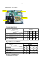
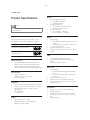
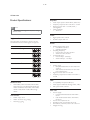
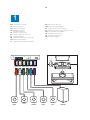
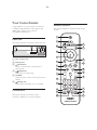
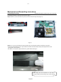
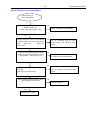
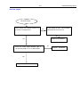
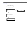
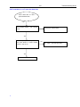
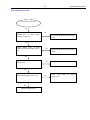
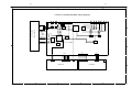
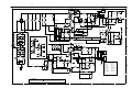
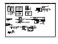
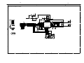
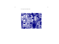
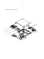
7-2 7-2 5 4 3 2 1 AV Board Circuit Diagram: SCART16 SCART8 D D 0V(CVBS) 6V(16:9) 12V(RGB) 9.5-12V(4:3) 0V(STANDBY) G/Y B/U D17 ESD0603/SMD/NC CVBS_O D16 ESD0603/SMD/NC R/V D14 ESD0603/SMD/NC D15 ESD0603/SMD/NC XP7 20 XP10 C 18 1 2 3 4 5 6 7 8 9 10 10PIN/2.0mm 1 2 3 4 5 6 7 8 9 10 SCART_R 16 SCART16 SCART_L B/U SCART8 G/Y R/V SCART16 CVBS_O 14 C73 680pF 12 10 8 SCART8 C77 SCART_L 0.1uF/25V C81 100pF 4 2 SCART_R ESD0603/SMD/NC D19 ESD0603/SMD/NC 6 D18 SHIELD VIN VOUT BLNKGND VGND BLNK R DATAGND RGND DATA G CLKOUT GGND SWITCH B AIL BGND AGND AOL AIR AOR C82 100pF 21 19 CVBS_O 17 15 R/V 13 C 11 G/Y 9 7 B/U 5 3 C80 100pF C76 100pF C74 100pF C72 100pF 1 SCART 21PIN B B A A 5 4 3 2 1 7-3 7-3 C D R540A CY506 R540B 470pF/250VAC Alternative 1 HV VDD 22 R540C T531 PQ3230 C531 4700pF/400VAC C533 1500pF/1KV 1 2 3 4 22 1 2 +33V D533 C538 0.1uF/50V/X7R 10A/200V CE503 + 100uF/400V D531A FR207/2A/1000V R532 NC D532 V U531 TOP258EN CONTROL C536 0 R548 100pF/1KV FR104/1A/400V T531F 6 P P-GND R572 10K/1% P FB 4 C535 0.1uF/50V/X7R R565 1K U532 BPC-817B 3 R539 R543 C534 OP 10K U533 AZ431LBZ C532 0.1uF/50V/X7R R502D Alternative CE532 10uF/50V ZD531 BZX79C8V2 CX502 0.33uF/250VAC CY501 470pF/250VAC 1 VDD CY502 470pF/250VAC R524 150 2 8 9 D562 T531P T5011 EEL19 Q561 NPN_MMBT8050CLT1 D HV CY503 7T501P5 A11 A12 11 T531N 12 R505A 150K R505B 150K R505C 150K C503 1000pF/1KV R505D 150K L503 3.3uH Alternative P 10 T501P24 P-GND T501 EF25 D505 FR107/1A/1000V XP501 T501P12 SR3100/3A/100V D513 + 9 Alternative Alternative NC FB T501F2 5 3 T501G1 8T501N S Drain NC 2 F501 4 T501D3 R507 BP/M D508 2 10 T501P24 S S EN/UV 1 1 R508 CY505 470pF/250VAC 22K 6 ZD502 BZX79C18 D506 + R504 1M 1M C504 2200pF/50V/X7R FR107/1A/1000V D514 MBRF1045/10A/45V FR107/1A/1000V + 8 D509 SR360/3A/60V C502 0.47uF/63V 2PIN/7.92mm R523 R515 NC D510 SR360/3A/60V Alternative 3.3uH 100 + CE509 2200uF/16V + CE510 1000uF/16V C505 R516 10K + CE511 1000uF/16V R518 2.49K/1% Alternative Alternative Alternative R511 470 R512 2.2K 1 2 U502 BPC-817B 3 ZD503 BZX79C11 4 2.2M M+5V PCON 3 CN502 8PIN/2.5mm/80mm 1 1:-24V 2 1 2:GND 3 2 3:+12V 4 3 4:GND 5 4 5 5:M+5V 6 6 6:M+5V 7 7 7:P_on/off 8 8 8:GND Alternative L502 CE504 47uF/35V R522 100K R526 1 2 3 4 5 6 7 8 R513 22 T501N 1N4148 1 2 1 2 CE505 10uF/16V CE508 47uF/50V T501F2 Q501 PNP_MMBT8550CLT1 Q502 PNP_MMBT8550CLT1 CN501 T501P5 D512 T501G4 D507 +12V FR107/1A/1000V +10V R509 R517 NC 8T501N 150 8 T3.15AH/250VAC R521 NC 8PIN/2.5mm 3 S VDR/560V 7 1 2 3 4 5 6 7 8 1 RV501 6 CE507 470uF/16V Alternative 7 U501 TNY179PN 1M + CE506 1000uF/16V Alternative 5 TR501 NTC/3ohm/5A R568 C563 1K 0.1uF/50V/X7R R564 1K C562 0.1uF/50V/X7R R514 22 CY504 6T501P5 T531F6 R563 1K D511 8T501N 470pF/250VAC R501 C561 0.1uF/50V/X7R 1 3 T501D NC 2 1K Alternative Alternative 470pF/250VAC HER203G/2A/200V T531G5 PNP_3CG3906M Q564 Q563 NPN_3DG3904M Q562 NPN_MMBT8050CLT1 MBRX120/20V/1A Remote on/off Standby mode: Q561, D561 OFF; D562 ON On mode: Q561, D561 ON; D562 OFF 9T501P12 C501 2200pF/1KV 6.6mH CX501 0.33uF/250VAC R502A R502B R579 1N4148 22 5 HV T531D3 R569 1K N.C LIF501 RV504 200V/500A R561 1.5K R560 A8 A9 R570 100 U561 BPC-817B R562 2.2K R533 NC D561 HV R546 NC ZD561 BZX79C33 OPP T5311 ER28 R505 150 1.5K R545 2.67K/1% 1 + R567 2 6.6mH R566 2.2K 0.1uF/50V/X7R 3 100 NC +33V 2.2K S X F CE531 + 47uF/35V NC OPP Circuit 110K/1% D535 1N4148 R573 1K R542 R525 150 2 1 C573 0.1uF/50V/X7R ZD532 BZX79C12 LIF502 R502C OP R574 CE537 22uF/50V R540 0 R538 6.8 R503 150 C571 0.1uF/50V/X7R 0 + C FB1 FB90@100MHz R571 10 mR R577 22K/1% 2 - R550 33.2K/1% R547 T531N T531G 5 D D536 1N4148 OPP D572 1N4148 1 M+5V 4 - R537 2M/5% R541 1K 10 12 A10 A12 C539 0.01uF/400V CE533 820uF/50V + R576 1K P U571A LM358/SO 1 CE502 + 100uF/400V D + 3 2 CE501 + 100uF/400V 3 CE535 820uF/50V C572 0.1uF/50V/X7R +10V 3 T531D + 1:+33V 2:+33V 3:+33V 4:GND 5:GND 6:GND 4 2 Alternative Alternative 1 Alternative C540 220pF/1KV 2 + 1 BD501 KBP306 R544 33.2K/1% N.C R531 NC + 1 M+5V 4 2 47K/2W R534 Q571 PNP_MMBT8550CLT1 R578 10K CN531 6PIN/2.5mm/70mm 1 2 1 3 2 4 3 5 4 6 5 6 2.9uH R549 0 R536 2M/5% R575 10 1 2 3 4 L531 8T531P 9 3 A8 A9 XP502 4PIN/2.5mm 8 Power Board Circuit Diagram: E 22 PCON B 3 A DVD mode T501:EEL19 U501:TNY177P +12V: D511:FR107 C503:NC R514:NC CE506:470uF/25V CE507:220uF/25V +5V: D510:NC CE509:1000uF/16V CE510:NC CE511:470uF/16V 3 0.1uF/50V/X7R U503 AZ431LBZ BD mode T501:EF25 U501:TNY179P +12V: D511:HER203 C503:1000pF/1kV R514:22/1206 CE506:1000uF/16V CE507:470uF/16V +5V: D510:SR360 CE509:2200uF/16V CE510:1000uF/16V CE511:1000uF/16V 1 4 2 4 R520 NC R519 2.4K/1% * CAUTION : THE PARTS MARKED WITH ARE IMPORTANT PARTS ON THE SAFETY. PLEASE USE THE PARTS HAVING THE DESIGNATED PARTS NUMBER WITHOUT FAIL. A B C D E 7-4 7-4 A B +12V: +12V(+-10%) +5V: +5V(+-2.5%) 8 7 6 5 4 3 2 1 TO POWER BOARD C D E Main Board Circuit Diagram: Power Supply R12 1K FB1 300/2A POWER_control POWER_c +5Vin 9 MO_VCC 8 7 6 5 4 3 2 1 C1 0.1uF/25V/Y5V 0603 XP3 8PIN/2.5mm Q1 ASM3403M + R14 C16 1uF/50V/Y5V 4.7K CE3 100uF/10V R3 200 C125 0.1uF/25V/Y5V 1 12-SM3403-0BX R2 200 1 EN1 A+5V MO_VCC U706 R819 1 C801 2.2uF/10V/Y5V VIN 2 VOUT 5 2.2 +3.3V_STB C800 1uF/10V/Y5V GND MO_VCC 3 EN NC FB5 LDO_G9091-330T11U CE1 47uF/16V C2 0.1uF/25V/Y5V +12V +12V 100mA C7 0.1uF/25V/Y5V AVCC 500/500mA + Q4 PNP_MMBT8550CLT1 +P12V AVCC 4 C11 + R7 22K CE2 0.1uF/25V/Y5V 47uF/16V R5 1K 2 2 LL4148 EN1 EN D72 9 PCON PCON R9 1K Q3 NPN_3DG3904M EN R10 10K NC R11 R74 NC/1.3K NC/27K Q32 NC/PNP_MMBT2907ALT1 +P12V R13 NC/4.7K Q5 NC/NPN_3DG9014M -P24V 3 R434 0/NC FB4 NC/500/500mA -24V 3 C10 NC/0.1uF/25V/Y5V MO_VCC D2 160mA RL207/2A/1000V R22 0.15 440mA 1000pF/50V/NP0 R337 0.82/2W TR_B1 10/1W 5 Q7 PNP_3CA8550D TR_B2 Q11 PNP_3CA8550D R26 5 R19 C13 V12 + CE6 470uF/6.3V C793 1000pF/50V/X7R C49 0.1uF/25V/Y5V 0 DV33 REGO2 R25 20K/1% C792 5 4 REGO1 + 1000pF/50V/X7R CE7 470uF/6.3V C47 0.1uF/25V/Y5V 5 R28 NC/10K/1% 4 R27 12K/1% A B C D E 7-5 7-5 5 4 3 2 1 Main Board Circuit Diagram: SPHE8202RQ-D FV33 0.1uF/25V/Y5V CE26 47uF/10V + RF3.3V Close to 8202RX-D FB20 SDRAM +3.3V 500/200mA SD33 8 8 8 8 Close to SDRAM 500/200mA 1000pF/50V/X7R TRACK_SR33 1000pF/50V/X7R FOCUS_SR34 R550 RFDA3.3V 0.1uF/25V/Y5V SPDL_S R24 0.1uF/25V/Y5V SLED_S R29 RF3.3V GAME_LCH GAME_CLK GAME_D0 GAME_D1 RF +3.3V Close to 8202R-D R20 10 DV33 AD_VCC3 Internal AD +3.3V C30 0.1uF/25V/Y5V CE30 10uF/10V SPHE8202RQ-D 500/200mA FB39 FB500/0.8A/NC DV33 2.2 AVCC3 + Internal DA +3.3V CE25 470uF/6.3V R205 R201 CE29 DAC_VREF R59 C43 2.2K FMIC R573 0 MIC SCART_CON 8 SCART1 MPEG_MUTE MIC 8 9 7 IR LL4148 M_A3 M_A2 M_A1 M_A0 M_A10 M_BA1 M_BA0 M_RAS M_CAS M_WE M_DQM0 M_A4 D75 IR_IN 7 9 SPDIF IR_IN IR R102 I2S_MCLK R480 I2S_BCLK R481 I2S_LRCK R482 I2S_DATA_IN R483 10K DVCC3 FMIC C50 1000P/50V/X7R M_A[0..11] M_D[0..15] M_BA[0..1] M_DQM[0..1] RAM_CLK M_CAS M_RAS M_WE 5 5 TRAY+ 6 LDSW/TRAY- 7 NC/500/800mA 500/800mA + CE14 CE17 C117 0.1uF/25V/Y5V 100uF/10V R53 DVDLDO Q10 PNP_MMBT8550CLT1 A+5V SP_MOT+ XOPVIP1 XOPVIN1 0.1uF/25V/Y5V GND 0.1uF/25V/Y5V R65 VINTK VINSL TR_B2 REGO1 RESET FWD VINLD REV GND GND GND DRVSB 27 VREF2 26 25 XP8 6PIN/2.0mm TRACK_S TR_B2 LOADLOAD+ OUTSW GND INSW 24 23 SLED_S 22 LOAD- 9 LOAD+ 10 SP_MOT- 11 1 12 FACT- 13 FACT+ 14 VCC1 VCTL VOTR- VCCD VOTR+ VCC2 VOSL+ VOLD- VOSL- VOLD+ VOFC- VOTK- VOFC+ VOTK+ 21 20 19 6 6 DQM[0..1] DCLK 6 6 CAS# RAS# WE# 6 6 6 1 2 3 4 5 REGO1 REGO2 TR_B1 TR_B2 I2S_DOUT2 I2S_DOUT1 I2S_DOUT0 DVDMDI MDI CDLDO LDO_CD DVDLDO LDO_DVD TXD MCU_RXD RXD MCU_TXD URST# MPEG_RST GND 1 2 3 4 5 LOADLOAD+ GND GND MA[0..11] DQ[0..15] BA[0..1] 6 4 4 4 4 +3.3V_STB SP_MOT+ SP_MOT- XP9 5PIN/2.0mm 30 M+5V GND 8 GND LDSW LDSW/TRAY- REGO2 BIAS 28 R64 4 REGO1 29 10K 5.1 FB25 FB26 E GND HOMESW IN_OUT_SW INSW TRAY_DECT TRAY_DECT I2S_DOUT2 I2S_DOUT1 I2S_DOUT0 10 10 10 MCU_RXD MCU_TXD MPEG_RST 9 9 9 B 9 GND 18 SL_MOT+ 17 SL_MOT- 16 TACT- 15 TACT+ AM5890S CDVR# DVDVR# PUH_CDLD# DVDMDI R58 0 R54 R55 R551 L11 GND GND A C121 + CDVR 0 CD_VR DVDVR 0 DVD_VR PUH_CDLD 10uH/280mA/NC DVDMDI CDMDI R552 0 PUH_DVDLD L10 10uH/280mA/NC 0 1000pF/50V/X7R C120 PUH_DVDLD# GND M+5V MO_VCC + 47uF/10V R57 R56 CE13 CDLDO Q9 PNP_MMBT8550CLT1 FACTFACT+ TACT+ TACTC D C102 C113 1000pF/50V/X7R GND VREF1 C119 XP2 24PIN/0.5mm + PUHRF A B F A+5V CE9 24 23 22 21 20 19 18 17 16 15 14 13 12 11 10 9 8 7 6 5 4 3 2 1 100uF/10V 24 23 22 21 20 19 18 17 16 15 14 13 12 11 10 9 8 7 6 5 4 3 2 1 0.1uF/25V/Y5V 27 28 A GND GND GND GND 26 25 GND SPDL_S RF3.3V 5.1 GND 47uF/10V 0.1uF/25V/Y5V C118 RF3.3V TR_B1 MUTE C DVCC3 4.7K 3 REGO2 VINFC SL_MOT+ SL_MOT- 1000pF/50V/X7R/NCC93 2 6 5 4 3 2 1 R63 1 TR_B1 6 5 4 3 2 1 4.7K FOCUS_S 0.1uF/25V/Y5V C15 Close to 8202RX-D 7 7 7 7 AMCLK ABCK ALRCK ASDATA0 FLASH SLEDSLED+ GND HOMESW SP+ SP- U7 AMCLK ABCK ALRCK ASDATA0 10 10 10 VIDEO INTERFACE 1000pF/50V/X7R/NC C116 VCC1.2 33 33 33 33 I2SMCLK I2SBCLK I2SLRCK U1 REGO1 REGO2 TR_B1 TR_B2 C34 C35 C48 C9 0.1uF/25V/Y5V 0.1uF/25V/Y5V 0.1uF/50V/Y5V 1000pF/50V/X7R B R204 I2S_MCLK I2S_BCLK I2S_LRCK AD_VCC3 1000pF/50V/X7R/NC C106 0 4.7K NC/4.7K 10uF/10V V12 R23 D 0.1uF/25V/Y5V INSW C29 0.1uF/25V/Y5V C33 0.1uF/25V/Y5V C257 0.1uF/25V/Y5V AVCC3 R30 GPIO25 M_A9 M_A8 M_A7 M_A6 M_A5 RAM_CLK 64 63 62 61 60 59 58 57 56 55 54 53 52 51 50 49 48 47 46 45 44 43 42 41 40 39 DVCC3 M_A11 0 DVCC3 FB34 4.7K 4.7K 4.7K RXD TXD M_D0 M_D1 M_D2 M_D3 M_D4 M_D5 M_D6 M_D7 M_D15 M_D14 M_D13 M_D12 M_D11 M_D10 M_D9 M_D8 M_DQM1 R577 R575 R576 VCC1.2 RFDA3.3V URST# RF3.3V 33 33 33 Video DAC +3.3V DVCC3 䚯ݽDA_AVDD noiseᒢᢠRF3.3Vሬ㠤D9н䈫 I2S_DOUT2 I2S_DOUT1 I2S_DOUT0 R21 0.1uF/25V/Y5V C32 + 47uF/10V CE23 0.1uF/25V/Y5V C31 VVCC3 I2S_LRCK I2S_BCLK I2S_MCLK Play 90mA Standby 8mA 500/200mA R583 R584 R585 Close to 8202RX-D FB31 NC/4.7K ADAC_AVSS ADAC_AVDD ADAC_AVDD VREF AOUT_LS AOUT_RS ADAC_AVSS AOUT_SUBW AOUT_CENTER AIN_R AD_AVDD AD_AVSS GPIO29 SPDIF_OUT M_A3 M_A2 M_A1 M_A0 M_A10 M_BA1/GPIO27 M_BA0 M_RAS M_CAS M_WE M_DQM0 M_A4 1 2 3 4 5 6 7 8 9 10 11 12 13 14 15 16 17 18 19 20 21 22 23 24 25 26 27 28 29 30 31 32 33 34 35 36 37 38 + 68K 20K 0 2.2K 2.2K DVDVR DRVSB IN_OUT_SW R60 1K TRAY+ CDVR SF_CS SPI_D0 SF_CK SPI_D1 I2S_DATA_IN 4.7K 4.7K C27 C28 CE21 + 0.1uF/25V/Y5V 100uF/10V0.1uF/25V/Y5V C 0.1uF/25V/Y5V C38 C39 R588 R589 FB30 C37 C40 C41 C273 4.7uF/16V/Y5V VREF1 VREF2 CDLDO DVDMDI CDMDI SRV_AVDD V21 V165 DA_AVSS DA_TEO DA_FEO DA_AVDD SPDC_OUT SC_OUT DVDVR DMEA SD_D1/GPIO4 SD_D0/GPIO5 SD_CLK/GPIO6 TRAYIN/SD_SMD/GPIO7 TRAYOUT/SD_D3/GPIO8 SD_D2/GPIO9 CDVR SPI_CE SPI_D0 SPI_CLK SPI_D1 TRAY+ 0 SF_CK SPI_D1 SPI_32Mb_EN25B32 R392 C36 103 104 105 106 107 108 109 110 111 112 113 114 115 116 117 118 119 120 121 122 123 124 125 126 127 128 CDLDO DVDMDI CDMDI + C22 C26 C24 C12 0.1uF/25V/Y5V 1000pF/50V/X7R 0.1uF/25V/Y5V 0.1uF/25V/Y5V 0.1uF/50V/Y5V 8 7 6 R195 5 4M/8M/16M bits VFD_CLK/GPIO16 VFD_STB/GPIO17 VFD_DATA/GPIO18 VDD_33 RESET_B VSS IR/GPIO19 GPIO20 GPIO21 VDD_18 M_DQM2/GPIO22 M_DQM3/GPIO23 M_D0 M_D1 M_D2 M_D3 M_D4 M_D5 M_D6 M_D7 M_D15 M_D14 M_D13 M_D12 M_D11 M_D10 M_D9 M_D8 M_DQM1 VSS M_CLK VDD_33 M_A11/GPIO25 M_A9 M_A8 M_A7 M_A6 M_A5 Digital C20 CE# VDD SO HOLD# WP# SCK VSS SI 1K CE27 47uF/10V + U176 1 2 3 4 NC/6.8pF/50V/NP0 C258 DVCC3 DVCC3 VCC1.2 + Close to 8202RX-D 500/200mA DVCC3 CE28 4PIN/2.0mm DV33 FB35 SF_CS SPI_D0 RF3.3V VCC1.2 R197 VVCC3 + 47uF/10V C254 1 2 3 4 102 DVDLDO DVDLDO 101 APC_AVSS 100 XOPVIN1 OPVIN 99 XOPVIP1 OPVIP 98 E CDE 97 F CDF 96 A DVDA 95 B DVDB 94 C DVDC 93 D DVDD1uF/10V/Y5V 92 C45 PUHRF RFIS 0.1uF/25V/Y5V 91 C44 AGCCAP 90 RF3.3V AD_AVDD 89 6 AD_AVSS 88 LDSW 6 LDSW/GPIO40 87 HOMESW 4.7K R32 HOME/GPIO39 86 VDD_18 85 XO CLKOUT 84 XI CLKIN 83 PLL_VDD 82 PLL_VSS 81 USB_AVSS 80 USB_DM USB_DM USB_DM 79 USB_DP USB_DP USB_DP 78 USB_AVDD 77 VDD_18 76 TV_AVSS 75 TV_DAC3 74 TV_DAC2 73 TV_DAC1 72 VVCC3 TV_AVDD 71 TV_AVSS 70 VVCC3 TV_AVDD 69 CVBS TV_DAC0 68 V_FSADJ 1K R31 V_FSADJ 67 V_COMP V_COMP 66 AOUT_R 65 AOUT_L C255 Put these Compnonents as closer as possible to MT1389 100pF/50V/NP0 GND 100pF/50V/NP0 TXD RXD 27MHz/30PPM C25 C21 33pF/50V/NP0 33pF/50V/NP0 D 1 2 3 4 XO 33 C256 R17 100pF/50V/NP0 Y1 R189 MO_VCC XP21 XI 4.7K 500/200mA 4.7K FB40 CE31 4.7K DV33 8 8 8 8 47uF/10V R16 V_R V_B V_G CVBS 0.1uF/25V/Y5V C46 CVBS GND 4 3 2 1 7-6 7-6 A B C D E Main Board Circuit Diagram: SDRAM & USB 1 1 U14 SDCLK SD33 2 38 37 DRAS# DCAS# DWE# 19 18 17 16 DQM0 DQM1 15 39 36 40 54 41 28 CLK CKE SD33 CS RAS CAS WE VCC VCC VCC VCCQ VCCQ VCCQ VCCQ DQML DQMH NC NC VSSQ VSSQ VSSQ VSSQ VSS VSS VSS 0.1uF/25V/Y5V C249 0.1uF/25V/Y5V C245 0.1uF/25V/Y5V C217 0.1uF/25V/Y5V C216 DQ7 DQ6 DQ5 DQ4 DQ3 DQ2 DQ1 DQ0 DQ8 DQ9 DQ10 DQ11 DQ12 DQ13 DQ14 DQ15 0.1uF/25V/Y5V C215 2 4 5 7 8 10 11 13 42 44 45 47 48 50 51 53 0.1uF/25V/Y5V C214 DQ0 DQ1 DQ2 DQ3 DQ4 DQ5 DQ6 DQ7 DQ8 DQ9 DQ10 DQ11 DQ12 DQ13 DQ14 DQ15 C23 A0 A1 A2 A3 A4 A5 A6 A7 A8 A9 A10/AP A11 BA0/A13 BA1/A12 0.1uF/25V/Y5V 23 24 25 26 29 30 31 32 33 34 22 35 20 21 1000pF/50V/X7RC238 1000pF/50V/X7RC238 SD33 MA0 MA1 MA2 MA3 MA4 MA5 MA6 MA7 MA8 MA9 MA10 MA11 DBA0 DBA1 DRAS# RAS# DWE# WE# 1 14 27 SD33 3 9 43 49 DCAS# CAS# DBA0 BA0 DBA1 BA1 SDCLK R402 6 12 46 52 33 DQ[0..15] DQ[0..15] MA[0..11] BA[0..1] DQM[0..1] DCLK CAS# RAS# WE# DCLK 5 MA[0..11] BA[0..1] DQM[0..1] DCLK 5 5 5 5 CAS# RAS# WE# 5 5 5 2 DRAM C219 10pF/50V/NP0 SDRAM_64Mb_M12L64164A-7T SDRAM XP22 +5Vin DP DM USB_DP USB_DM R569 F4 W=1mm 1 2 3 4 4PIN/2.0mm C156 R389 R390 3 VCC_USB NC/0 Q46 PNP_PBSS5320T PTC/1.5A/6V 1 2 3 4 5 5 100pF/50V/NP0 ESD8 3 ESD9 33pF/50V/NP0 200 200 33pF/50V/NP0 MO_VCC P_CTR R4 10K Q2 NPN_3DG3904M USB BLOCK 4 4 A B C D E 7-7 7-7 5 4 3 2 1 Main Board Circuit Diagram: AUDIO_IN TUNER_L TUNER_R 9 9 1uF/16V/Y5V AL_CH2 C163 100pF/50V/NP0 C811 100pF/50V/NP0C811 100pF/50V/NP0 C810 100pF/50V/NP0C810 R97 TUNER_R 10K R104 AUX_L R87 1uF/16V/Y5V AL_CH3 C166 10K R154 3K/NC 1M 1uF/16V/Y5V AR_CH2 C164 AUX_R R91 1uF/16V/Y5V AR_CH3 C167 10K C73 0.1uF/25V/Y5V R162 22K NC/1M R176 NC/1M AR_CH2 R153 2.7K + R177 NC/1M AL_CH1 CE32 R178 NC/1M AR_CH1 47uF/16V R163 22K AR_CH1 AR_CH2 AR_CH3 AR_CH4 12 14 15 11 AL_CH1 AL_CH2 AL_CH3 AL_CH4 1 5 2 4 4052_SLCTA R1239 4052_SLCTB R1319 10 9 470 470 6 7 MIC 1uF/16V/Y5V AL_CH4 C169 MP3_AL R105 X0 X1 X2 X3 VCC D X Y0 Y1 Y2 Y3 Y A74HC4052 B EN VEE GND 16 1uF/16V/Y5V LA C175 MIC_R 13 1uF/16V/Y5V LB C174 MIC_L 3 470 AD_INR R94 R95 100K 470 AD_INL R98 100K 8 R93 C74 470pF/50V/X7R C75 470pF/50V/X7R +12VA DV33 R435 R437 22K 1uF/16V/Y5V AR_CH4 C170 MP3_AR 1uF/16V/Y5V MIC_L C176 47K +6VA R158 8.2K 5.6K MIC_R NC/0 R107 2K R100 R99 4.7K 4.7K R103 1uF/16V/Y5V C168 + CE46 47uF/16V U6 R174 NC/1M 4052_SLCTA 4052_SLCTB 47K R198 +6VA NC/1M AL_CH4 R173 NC/1M AR_CH4 R175 AL_CH2 R157 3K/NC +6VA R88 AR_CH3 R165 NC/1M R118 2.7K R155 3K/NC MIC_LR 1M R166 R160 8.2K 5.6K R156 3K/NC 22K R436 + 0.1uF/25V/Y5V 10K MIC_LR R167 LB AL_CH3 R164 R92 TUNER_L D LA C154 TUNER_L TUNER_R 100 +12V CE49 100uF/16V C C AVCC C139 R216 + CE48 100uF/16V C80 0.1uF/25V/Y5V R116 4.7 R119 47K 8 MP3_AL MP3_AL 9 R218 MP3_AR MP3_AR 9 MIC_LR MIC_LR 9 AD_INR 1K C158 0.1uF/25V/Y5V 3 + 2 - 1 C172 U184A F4558 4 1 2 3 4 5 DV33 2.2 10K 5PIN/2.0mm XP10 1 2 3 4 5 R553 47pF/50V/NP0 R253 1V ADC_INR 5.6K 10uF/10V/Y5V 1V MIC 1 2 3 4 5 6 7 8 R220 100K/NC C143 47pF/50V/NP0 R226 MIC 10K + CE47 10uF/10V 4 R225 100K/NC 5 R254 CKS0 CKS2 DIF PDN SCLK MCLK LRCK SDTO R117 9 ADC_RST AUX_L +12VA 1K 1 4 5 B AUX_R CVBS_O 5 5 5 5 10uF/10V/Y5V +6VA 3 ABCK AMCLK ALRCK ASDATA0 U8 ADC_AK5358A 0.1uF/25V/Y5V P2 16 15 14 13 12 11 10 9 C79 0.1uF/25V/Y5V ADC_INL 5.6K AINR AINL CKS1 VCOM AGND VA VD DGND 8 C159 6 - 1K + AD_INL R227 F4558 U184B 7 C173 R121 10K ADC_INR ADC_INL +6VA 5 R120 10K 8 CVBS_O B 2 C97 DV33 6 100pF/50V/NP0 RCA/4h R101 SPD_VCC 10K R815 10 U709 L12 1.8uH/25mA 0.1uF/25V/Y5V C160 R814 1 100 R96 PESD5V0S1BA/30K/35pF D612 10K 3 5 C370 C381 100pF/50V/NP0 100pF/50V/NP0 R368 75 9 11 2 1 COAX_IN 13 7 1A 1Y 2A 2Y 3A 3Y 4A 4Y 5A 5Y 6A 6Y GNDVCC 2 4 1 6 2 8 3 10 SPDIF_IN2 B2 S GND VCC B1 A 6 R228 1K SPDIF_SW SPDIF_SW 9 SPDIF 5 5 4 C161 0.1uF/25V/Y5V U707 TS5A3159 12 14 C162 0.1uF/25V/Y5V SPD_VCC 74HC04PW C165 0.1uF/25V/Y5V SPDIF IN OPTI GND R124 NC/200 3 C108 2 0.1uF/25V/Y5V 1 +5V OPTICAL IN P4 R816 R108 C84 330pF/50V/X7R R110 NC/0 R109 NC/0 SPDIF_IN2 0 DV33 10 C52 1uF/10V/Y5V A A 5 4 3 2 1 7-8 7-8 5 4 3 2 1 Main Board Circuit Diagram: Video Out V+5V NC/RCA/3h R545 1 L9 1.2uH/25mA CE18 47uF/10V R555 CVBS_O R/V AVCC R549 C103 100pF/50V/NP0 P5 V_R V_B V_G 2.2 C92 0.1uF/25V/Y5V G/Y 7 5 5 5 CVBS_O V_R V_B V_G D VIDEO I/F CVBS_O 0 C104 100pF/50V/NP0 NC/100 NC/1.2K 75 100pF/50V/NP0 C67 R82 D B/U V+5V 5 Q23 NC/NPN_3DG3904M R547 CVBS 100pF/50V/NP0 C66 CVBS C101 100pF/50V/NP0 2 + 5 3 4 10pF/50V/NP0/NC R546 NC/2.4K C65 R548 NC/33 SCART1 SCART2 SCART_CON 5,8 SCART1 5,8 SCART2 8,9 SCART I/F Vedio out L3 C PESD5V0S1BA/30K/35pF D7 1 PESD5V0S1BA/30K/35pF D6 R/V PESD5V0S1BA/30K/35pF D8 2 PESD5V0S1BA/30K/35pF D5 2 R127 C85 75 100pF/50V/NP0 CVBS_O 1 1 B/U 2 G/Y 1 R/V 1.2uH/25mA 2 V_R C L4 B/U 1.2uH/25mA R132 C86 75 100pF/50V/NP0 MO_VCC L5 V_G 2.2 C98 0.1uF/25V/Y5V G/Y 1.2uH/25mA R136 C87 75 100pF/50V/NP0 XP703 1 2 3 4 5 6 1 2 3 4 5 6 R812 220 R813 220 R586 R587 R556 R484 R485 R486 R487 22 22 22 22 4.7K 4.7K V_B GAME_D0 GAME_D1 NPN_3DG3904M Q703 GAME_D0 GAME_D1 5 5 GAME_CLK NPN_3DG3904M Q704 GAME_LCH GAME_CLK 5 GAME_LCH 5 6PIN/2.0mm GAME PAD AVCC SCART16 C96 7PIN/2.0mm 1 2 3 4 5 6 7 B R125 1 2 3 4 5 6 7 R128 4.7K B/U SCART8 G/Y R/V SCART16 CVBS_O R129 XP11 SCART8 DV33 Q28 NPN_3DG3904M R126 1K 0.1uF/25V/Y5V 150 1.5K R130 1.5K R133 B SCART_CON 2.2K SCART_CON 5,8 SCART_CON +12V SCART16 0 CVBS OUT 1 RGB OUT ZD5 12V R135 1K SCART2 DV33 R137 4.7K R138 2.2K 0 SCART8 0(STANDBY) 1 5,8 SCART1 Q25 NPN_3DG3904M SCART1 1 6V(16:9) 0 9.5-12V(4:3) DV33 0 R139 4.7K Q26 NPN_3DG3904M R140 2.2K SCART2 8,9 A A 5 4 3 2 1 7-9 7-9 5 4 3 2 1 Main Board Circuit Diagram: MCU & CONNECTOR D D +3.3V_STB R425 1M +3.3V_STB Y4 YO YI 12MHz/30PPM D73 MCU_RST C91 20pF/50V/NP0 R106 10K LL4148 NC/0.1uF/25V/Y5V C239 R559 +3.3V_STB C94 20pF/50V/NP0 MCU_RST U33 1 2 3 4 NC NC NC GND VCC WP SCL SDA 8 7 6 5 NC/4.7K WP MCU_SCL MCU_SDA NC/EEPROM_16Kb_AF24BC16 SOP8-244-1.27 +3.3V_STB R149 10uF/10V CE254 VOLPOWER_control POWER_ON/OFF PDN AMP_RST 33 33 33 0 NC/0 0 7 8 OP_CL VOL+ YO YI C95 C 16PIN/1.0mm TO FB BD DV33 +3.3V_STB C89 0.1uF/25V/Y5V + DV33 TPA TPB 16 15 14 13 12 11 10 9 8 7 6 5 4 3 2 1 0.1uF/25V/Y5V SPDIF_SW SCART2 TP45 BKND_ERR C90 R579 R578 NC/4.7K NC/4.7K C806 NC/33 NC/33 100pF/50V/NP0 R505 R506 TP48 P/RESET 0 C805 TP43 TP46 TP47 R527 0.1uF/25V/Y5V VOLVOL+ DV33 MP3_AL 33 C804 4.7K 4.7K MP3_AR MP3_AL 100pF/50V/NP0 PWM2 SPISS0 TXD1 RXD1 T3 T2 AVDD VDD CTS1 RTS1 CTS0 RTS0 13 14 15 16 17 18 19 20 21 22 23 24 R147 WP TUNER_SCL R150 TUNER_SDA R148 MIC_DET TUNER_reset TU_SEN ICE_DAT ICE_CLK MP3_AR 7 16 15 14 13 12 11 10 9 8 7 6 5 4 3 2 1 AMP_RST 1/2power-control B TP49 1/2power-control 11 PCON 4 POWER_control 4 DV33 R539 PDWN DSP_RESET NC/0 P/RESET R525 SDA SCL MCU_SDA MCU_SCL 4.7K 10 10 IR_IN Power MCU_SDA MCU_SCL 4.7K 5 TXD1 TP40 IR_IN M054LAN 36 35 34 33 32 31 30 29 28 27 26 25 7 R538 R537 +12V MO_VCC -24V PWM1 SPISS1 MOSI_1 MISO_1 SPICLK1 ICE_DAT ICE_CLK ALE /CS PWM7 PWM6 PWM5 MIC_LR C803 MCU_RST RXD1 MOSI_0 MISO_0 SPICLK0 RST RXD AVSS TXD STADC MCLK SDA/T0 SCL PWM3 MIC_LR Power R501 IR_IN CS R502 Din/out R503 CLK R504 R534 +5Vin CKO RD XTAL2 XTAL1 VSS LDO_CAP PWM0 PWM1 PWM2 PWM3 PWM4 PWM0 SPI_DAT SPI_CLK 1 2 3 4 5 6 7 8 9 10 11 12 7 100pF/50V/NP0 4.7K U182 TP41 R554 5 TRAY_DECT XP33 R134 10K 5 7 7 7 ADC_RST 4052_SLCTA 4052_SLCTB 1K R580 MCU_RXD MCU_TXD MPEG_RST CS CLK Din/out 48 47 46 45 44 43 42 41 40 39 38 37 5 MUTE RX R581 4.7K TX5 SPI_CS 0.1uF/25V/Y5V C264 100 R526 C +3.3V_STB SPI_CS SPI_CLK SPI_DAT +3.3V_STB 100pF/50V/NP0 CE255 10uF/10V 1000pF/50V/X7RC265 1000pF/50V/X7RC265 + TH_WAR 11 PDN DSP_RESET 10 10 B 2 MUTE 4.7K +3.3V_STB 5PIN/2.5mm 5 4 3 2 1 5 4 3 2 1 1 5 MPEG_MUTE ICE_DAT ICE_CLK MCU_RST 3 AMP_MUTE D21 BAT54C AMP_MUTE 10 XP1 XP36 2 1 RFGND U183 R533 2 1 2 1 3PIN/2.5mm 1 2 3 4 5 6 7 NC/0 0 ESD10 NC/ESD_8KV DV33 AGND R151 1K 100pF/50V/NP0 C809 100pF/50V/NP0C809 RFGND R152 RF_GND IISD FM_ANT VCC_GND AM_ANT1 L_OUT AM_ANT2 R_OUT RF_GND DA IIC/RDSI CK LA VCC MK004FX1-R808B 14 13 12 11 10 9 8 AGND 100pF/50V/NP0 C808 100pF/50V/NP0C808 XP35 100pF/50V/NP0 C807 100pF/50V/NP0C807 2 1 NC/2PIN_2.5 AGND C267 1uF/16V/Y5V C266 1uF/16V/Y5V TUNER_SDA R530 0 TUNER_SCL R531 0 L13 TUNER_L TUNER_R 1.8uH/25mA Q27 NC/NPN_MMBT8050C L14 NC/1.8uH/25mA + CE65 100uF/10V 0.1uF/25V/Y5V R359 NC/150 C130 7 7 FB21 500/500mA FB22 500/500mA FB23 500/500mA DV33 AGND AVCC ZD4 AGND C394 NC/1uF/16V/Y5V NC/BZV55C3V9/3.9V A A AGND 5 4 3 7-10 7-10 A B C D E Main Board Circuit Diagram: STA309A 1 1 VD3.3V D705 LL4148 Q702 PNP_MMBT8550CLT1 R739 VD3.3V 47K C716 4.7K Q701 D VD3.3V NPN_3DG3904M R796 47K D C706 C707 15pF/50V/NP0 C710 R798 VD3.3V 10K D MOV GND VDD3.3 GND NC SDI_78 SDI_56 SDI_34 SDI_12 LRCK1 BICK1 VDD3.3 GND NC RESET PLLB STA309A OUT2A OUT2B NC GND VDD OUT3A OUT3B OUT4A OUT4B OUT5A OUT5B NC GND VDD3.3V OUT6A OUT6B 48 47 46 45 44 43 42 41 40 39 38 37 36 35 34 33 CH3A CH4A CH5A C721 CH1A 11 CH2A 11 VD3.3V C720 C719 47pF/50V/NP0 11 11 C73311 C717 0.1uF/25V/Y5V D 2 C732 VD3.3V 47pF/50V/NP0 + C718 0.1uF/25V/Y5V CH6A CH6B 11 11 CE721 22uF/16V D C712 17 18 19 20 21 22 23 24 25 26 27 28 29 30 31 32 C705 D 22uF/16V D 1 2 3 4 5 6 7 8 9 10 11 12 13 14 15 16 0.1uF/25V/Y5V 15pF/50V/NP0 33 33 33 33 33 33 33 33 33 0.1uF/25V/Y5V + CE717 C731 0.1uF/25V/Y5V C701 VD3.3V 15pF/50V/NP0 FB712 500/800mA C702 DV33 C713 0.1uF/25V/Y5V R701 R703 R702 R709 R708 R707 R706 R705 R704 47pF/50V/NP0 +3.3V RESET SDA SCL ASDAT2 ASDAT1 ASDAT0 LRCLK BLCK MLCK R712 10K 11 EAPD R767 1K U703 TP42 C715 0.1uF/25V/Y5V 33 47pF/50V/NP0 FB711 500/800mA PDWN R711 47pF/50V/NP0 2 9 9 5 5 5 5 5 5 9 9 9 15pF/50V/NP0 MCU_SDA MCU_SCL I2S_DOUT2 I2S_DOUT1 I2S_DOUT0 I2SLRCK I2SBCLK I2SMCLK AMP_MUTE DSP_RESET PDN 15pF/50V/NP0 SDA SCL ASDAT2 ASDAT1 ASDAT0 LRCLK BLCK MLCK AMP_MUTE RESET PDWN C714 0.1uF/25V/Y5V 64 63 62 61 60 59 58 57 56 55 54 53 52 51 50 49 R805 PDWN SDIO_78 SDIO_56 NC GND VDD SDO_34 SDI_12 LRCKO BICKO NC GND VDD EPAD OUT1A OUT1B AMP_MUTE 0.1uF/25V/Y5V CE723 100uF/10V SA SDA SCL XT1 FIL NC GNDA VDDA CKOUT NC GND VDD3.3 OUT8_B OUT8_A OUT7_B OUT7_A + C723 C725 47pF/50V/NP0 D 47pF/50V/NP0 D D R777 10K R713 10K C724 0.1uF/25V/Y5V D VD3.3V D R714 3.3K FB715 500/800mA 3 3 C727 C729 1200pF/50V/X7R 100pF/50V/NP0 C728 220pF/50V/NP0 C730 0.1uF/25V/Y5V + CE704 C726 0.1uF/25V/Y5V 22uF/16V R799 0 D 4 4 A B C D E 7-11 7-11 A B C D E Main Board Circuit Diagram: STA518 29 28 TH_WAR R817 NC/0 27 + CE705 100uF/16V C745 0.1uF/25V/Y5V 10,11 R717 10K 26 25 EAPD 24 22 0.1uF/25V/Y5V C747 21 20 0.1uF/50V/Y5V 19 OUT2A TH-WAR OUT2A FAULT OUT1B TRI-STATE OUT1B PWRDN VCC1B CONFIG GND1B VL GND1A VDD VCC1A VDD OUT1A GND-Reg OUT1A GND-CLEAN 0.1uF/50V/X7R C456 0.1uF/50V/X7R 8 L708 C451 0.1uF/50V/X7R D C453 0.1uF/50V/X7R D 1 JK701 SPK JACK 22uH/3.3A L703 10 22uH/3.3A 11 C752 R719 12 10 1uF//50V/X7R 13 C751 680pF/50V/X7R R727 10 C749 17 C459 0.1uF/50V/X7R R722 4.7K C764 15 16 0.47uF/63V 680pF/50V/X7R R406 4.7K 0.1uF/50V/X7R L704 D C768 0.47uF/63V C458 0.1uF/50V/X7R R729 4.7K 22uH/3.3A CE711 220uF35V CE713 220uF35V C461 CE714 220uF35V 0.1uF/50V/X7R +35.5V 18 CE715 220uF35V CE719 220uF35V +35.5V + + CE718 220uF35V CE716 220uF35V + 820uF/50V R723 4.7K + C750 0.1uF/50V/X7R + CE710 SUBSUB+ SLSL+ SRSR+ CENCEN+ FLFL+ FRFR+ C460 0.1uF/50V/X7R CE712 220uF35V C748 1uF//50V/X7R C741 14 STA518 D R728 4.7K 32 CH5A 31 10 30 CH1A 10 29 CH2A 11,9 28 TH_WAR R735 NC/0 27 25 24 +3.3V R557 23 2.2 CE708 + 22 C798 100uF/16V 0.1uF/25V/Y5V C758 21 0.1uF/50V/Y5V 20 19 GND2B IN2A GND2A IN1B VCC2A IN1A OUT2A TH-WAR OUT2A FAULT OUT1B TRI-STATE OUT1B PWRDN VCC1B CONFIG GND1B VL GND1A VDD VCC1A VDD OUT1A GND-Reg OUT1A GND-CLEAN 4 R720 10 1uF//50V/X7R C742 C789 5 0.47uF/63V 7 R725 4.7K C760 10 L706 12 D 22uH/3.3A R731 10 13 1uF//50V/X7R C759 1uF//50V/X7R C746 14 15 16 C766 680pF/50V/X7R C762 R733 10 17 18 NC C767 D 680pF/50V/X7R L707 C770 0.47uF/63V R732 4.7K D C771 0.47uF/63V R734 4.7K D C464 0.1uF/50V/X7R 22uH/3.3A + C763 0.1uF/50V/X7R D706 4.7uF/50V R773 15K 4 - 2 + 3 D R742 10K CE733 D707 LL4148 D708 LL4148 4.7uF/50V R743 10K 3 SUB+ SL+ + CE734 8 C785 R766 18K R770 NC/150K 4.7uF/50V + CE730 R772 1.5K/1% CE735 100uF/16V D709 LL4148 D710 LL4148 4.7uF/50V + R761 NC/10 R769 15K/1% CE736 4.7uF/50V R745 10K SR+ R746 10K FR+ FL+ + D C783 0.1uF/25V/Y5V R744 10K + +12V LL4148 + CE732 4.7uF/50V +35.5V +35.5V CE709 0.1uF/25V/Y5V + D C463 0.1uF/50V/X7R CE740 R771 2.7K TP21 TP22 TP23 TP24 4PIN/2.5mm D 9 1/2power-control 4 3 2 1 0.1uF/50V/X7R 820uF/50V R765 5.6K 4 3 2 1 11 STA518 F4558 U705A 1 XS703 0.1uF/50V/X7R D 3 R726 4.7K D 8 9 C462 0.1uF/50V/X7R R754 4.7K 680pF/50V/X7R C739 1uF//50V/X7R 6 C744 C765 0.1uF/50V/X7R 26 R736 0.1uF/25V/Y5V 10K EAPD VCC2B IN2B 2 3 C774 0.1uF/50V/X7R 10,11 C756 VSS D 22uH/3.3A C769 0.1uF/50V/X7R + CE707 100uF/16V OUT2B L705 C466 D 10 VSS 2 C467 33 OUT2B 0.1uF/50V/X7R 34 VCC-Sign 0.1uF/50V/X7R C754 0.1uF/50V/X7R CE724 220uF35V 1 C465 C755 0.1uF/50V/X7R SUB-GND 0.1uF/50V/X7R 2 VCC-Sign + 35 CE720 220uF35V + U702 36 D GND GND 12 11 10 9 8 7 6 5 4 3 2 1 9 NC D C455 C743 0.1uF/50V/X7R 0.47uF/63V + 100uF/16V + IN1A 7 R403 6.2 + CE706 C797 VCC2A 6 R404 6.2 + 23 2.2 IN1B 680pF/50V/X7R C457 C738 0.1uF/50V/X7R C736 C737 + R558 +3.3V GND2A C740 1uF//50V/X7R 5 C452 0.1uF/50V/X7R 12 11 10 9 8 7 6 5 4 3 2 1 C472 CH4A 11,9 IN2A 4 R718 10 SUBSUB+ SLSL+ SRSR+ CENCEN+ FLFL+ FRFR+ C471 10 30 GND2B C454 0.1uF/50V/X7R 0.1uF/50V/X7R CH3A VCC2B IN2B TP26 TP27 TP28 TP29 TP30 TP31 TP32 TP33 TP34 TP35 TP36 TP37 22uH/3.3A 1uF//50V/X7R C470 10 31 OUT2B VSS L702 3 0.1uF/50V/X7R CH6B 2 C469 10 32 VSS 1 0.1uF/50V/X7R 1 CH6A OUT2B 0.1uF/50V/X7R 33 D 10 34 SUB-GND VCC-Sign C468 C735 0.1uF/50V/X7R 0.1uF/50V/X7R C734 0.1uF/50V/X7R VCC-Sign D 35 13 14 U701 36 CE737 D711 LL4148 4.7uF/50V R747 10K CEN+ + D D SL- R568 33 SR- R570 33 CEN- R572 33 +35.5V R806 R807 R808 47K 47K 47K 4 33 F4558 U705B 7 6 5 R567 8 33 R566 + R565 FR- - FL- R811 47K 22K R571 22K C782 0.1uF/25V/Y5V ZD3 BZV55C15V D R818 R809 R810 47K 47K D D 0 4 4 R561 8.2K C781 0.1uF/25V/Y5V D A B ZD2 NC/RLZ8.2B/8.2V D C D E 7-12 7-12 Front Control Board Print-layout (Bottom Side): 7-13 7-13 AV Board Print-layout (Bottom Side): 7-14 7-14 Power Supply Print-layout (Bottom Side): 7-15 7-15 Main Board Print-layout (Top Side): 7-16 7-16 Main Board Print-layout (Bottom Side): 8-1 Exploded View for HTS2511/12/05: 8-2 Exploded View for HTS2511/55/98/94: 9-1 REVISION LIST Version 1.0 * Initial release for HTS2511/12/55 Version 1.1 * Initial release for HTS2511/98 Version 1. 2 * Initial release for HTS2511/94 Version 1. 3 * Initial release for HTS2511/05