1
Embedding it better...
µTasker Document
• SMT32 Developer’s Document
uTaskerV1.4_Developers_Document/0.5
Copyright © 2012 M.J.Butcher Consulting
www.uTasker.com
µTasker – STM32 Developer’s Document
Table of Contents
1.
2.
3.
4.
Introduction ....................................................................................................................3
Preparing to work with the STM32 .................................................................................4
First Steps with the STM32.............................................................................................6
Blinking an LED .............................................................................................................8
4.1. F1 GPIOs................................................................................................................9
4.2. F2/F4 GPIOs ........................................................................................................11
4.3. F4 System Clock ..................................................................................................12
4.4. F2 System Clock ..................................................................................................13
4.5. F1 System Clock ..................................................................................................13
4.6. Cortex M3/M4 peripherals ..................................................................................15
5. Using the STM32 UART ..............................................................................................16
5.1. F1 Peripheral Configuration ................................................................................16
5.2. F2/F4 Peripheral Configuration ..........................................................................17
6. Ethernet ........................................................................................................................19
6.1. STM3210C-EVAL ................................................................................................19
6.2. STM3240G-EVAL ................................................................................................20
6.3. Checksum Offloading ..........................................................................................20
7. FLASH .........................................................................................................................21
7.1. F1 Flash ................................................................................................................21
7.2. F2/F4 Flash ..........................................................................................................21
8. External Interrupts (EXTI) ............................................................................................23
9. SPI FLASH ..................................................................................................................23
10. SD Card .....................................................................................................................24
11. Flexible Static Memory Controller .............................................................................24
12. USB Full-Speed Device .............................................................................................25
13. Conclusion .................................................................................................................27
APPENDIX A - STM32F1, STM32L and STM32W ............................................................28
APPENDIX B – STM32F2xx ...............................................................................................32
APPENDIX C – STM32F4xx ...............................................................................................34
APPENDIX D – Building the µTasker Project in the µTasker Simulator and generating a
cross-compiled Object for the HW Target.............................................................................35
APPENDIX E – Working with the µTasker Project and Rowely CrossWorks.......................39
APPENDIX F – Working with the µTasker Project and Atollic TrueSTUDIO ......................41
APPENDIX G – Working with the µTasker Project and IAR ...............................................43
APPENDIX H – Working with the µTasker Project and Keil uVision ..................................44
APPENDIX I – STM3240G-EVAL Modification to allow full Demo Functionality .............45
uTaskerV1.4_Developers_Document/0.5
2/46
22.02.2012
www.uTasker.com
µTasker – STM32 Developer’s Document
1. Introduction
This guide is a result of practical work during porting the µTasker project to the STMicro STM32 family of devices and covers the SMT32F1xx, STM32F2xx and
STM32F4xx Cortex M3 and M4 based microcontrollers and their internal resources
(memory, peripherals etc.). The document explains many details which are possibly
not immediately obvious from initial study of the extensive ST-Micro documentation,
including data sheets and user’s manuals; however it isn’t intended to replace these
sources of information.
Many details included explain the base of the implementation for the µTasker STM32
project, where readers can then better understand the choice of methods when
working with the project or better build on the base for further study of the µTasker
project code and methods.
The µTasker project intends to give support to developments based on the STM32
family of devices and includes various IDE projects so that users can efficiently work
with their chosen tools - the following environments are included:
-
GCC Make File build (without IDE for target debugging but useable together
with the µTasker simulator as a post-build step)
-
Rowley Crossworks
-
Atollic TrueSTUDIO
-
IAR
-
Keil uVision
The µTasker project is supported in these environments, which means that the
projects are verified as best as possible in all environments and experience with the
tools is collected to allow help to be provided where possible.
Quick start guides to working with the µTasker project in these environments are
included in the appendixes.
It is further to be noted that the µTasker project is designed to operate within all
environments, meaning that there are not completely different projects for each
cross-compiler. This also has advantages when evaluating IDEs to be used for
project development since it is possible to have the project open in all possible
development environments at the same time and any code changes to the project
made in one will be valid for others too. Targets can be thus tested with multiple IDEs
at the same time with the only restriction being that only one can actually be attached
to the debugger at any time.
uTaskerV1.4_Developers_Document/0.5
3/46
22.02.2012
www.uTasker.com
µTasker – STM32 Developer’s Document
2. Preparing to work with the STM32
The STM32F1xx and STM32F2xx family of devices are based on the ARM Cortex
M3 and the STM32F4xx family on the ARM Cortex M4. The Cortex M4 can be
considered to be a Cortex M3 with an increased instruction set, including additional
DSP like instructions and optional Floating Point Unit. This means that the Cortex M4
based parts can be more efficient in terms of execution speed of code and algorithms
that can make use of the additional instructions; the programmer doesn’t however
have to be fully aware of the differences when moving between Cortex M3 and
Cortex M4 based processors – code will essentially run on both without any changes,
where the compiler will make decisions as to the best way to actually use the
instruction set of the core available.
The STM32F4xx Cortex M4 based devices are however newer and thus contain
many other optimisations in terms of bus structure, memory and peripherals and
these details tend to be the most important differences in terms of actual project
development; although core code is compatible between the devices the peripheral
code can vary greatly.
In order to start work with the STM32 devices the following tools are required:
-
A development/evaluation board with the processor so that code can be
executed and internal/external peripherals controlled
-
A development environment allowing code to be written and compiled to a
format that can be loaded to the memory of the processor
-
Preferably a debugging environment allowing the processor/boards’s memory
to be viewed, and code execution to be manipulated (breakpoints, instruction
viewer, stepping, etc.)
The µTasker simulator allows a great deal of the code to be tested and the device’s
functionality to be verified without any of the tools above. It also allows increased
development and debugging efficiency in many cases as a compliment to these tools.
At some point it will however be necessary to have basic capabilities as listed above
to verify target operation in a real project.
The µTasker project supports essentially all STM32 device; F1, F2 and F4 families in
all sizes and packages. The µTasker demonstration project can be built to run on,
and simulate, any of these by configuring the processor/board in the file config.h.
//#define
//#define
//#define
#define
STM3210C_EVAL
STM3240G_EVAL
ST_MB913C_DISCOVERY
ST_MB997A_DISCOVERY
//
//
//
//
evaluation board with STM32F107VCT
evaluation board with STM32F407IGH6
discovery board with STM32F100RB
discovery board with STM32F407VGT6
Here four standard boards are shown, whereby one of them
(ST_MB997A_DISCOVERY) is activated for the build. Users can add their own boards
to the list.
uTaskerV1.4_Developers_Document/0.5
4/46
22.02.2012
www.uTasker.com
µTasker – STM32 Developer’s Document
In the file app_hw_stm32.h the STM32 part is specified and additional details
concerning the board and the exact hardware details of the project are configured.
The following shows the processor setup for the board above
#define
//#define
//#define
#define
CRYSTAL_FREQ
DISABLE_PLL
USE_HSI_CLOCK
PLL_INPUT_DIV
#define PLL_VCO_MUL
#define PLL_POST_DIVIDE
#define
#define
#define
#define
#define
#define
#define
#define
#define
PIN_COUNT
PACKAGE_TYPE
_STM32F4XX
SIZE_OF_RAM
SIZE_OF_CCM
SIZE_OF_FLASH
SUPPLY_VOLTAGE
PCLK1_DIVIDE
PCLK2_DIVIDE
8000000
// run from clock source directly
// use internal HSI clock source
4
// 2..64 - should set the input to pll in
the range 1..2MHz (with preference near to 2MHz)
168
// 64 ..432 where VCO must be 64..432MHz
2
// post divide VCO by 2, 4, 6, or 8 to get the
system clock speed
PIN_COUNT_100_PIN
PACKAGE_LQFP
(128 * 1024)
(64 * 1024)
(1024 * 1024)
SUPPLY_2_7__3_6
4
2
//
//
//
//
128k SRAM
64k Core Coupled Memory
1M FLASH
power supply is in the range 2.7V..3.6V
The details allow the project to configure itself according to the chip, whereby the
simulator knows which family type and package is being used and adapts itself to suit
it. Details about the clock configuration details are given later in this document.
uTaskerV1.4_Developers_Document/0.5
5/46
22.02.2012
www.uTasker.com
µTasker – STM32 Developer’s Document
3. First Steps with the STM32
The first thing that needs to be known is how the STM32 starts, which means what
the processor actually does when power is applied to the board and the reset line is
negated. The exact behaviour is in fact STM32 family dependent since some devices
include an internal boot loader which can start in this case and allow the user to load
code to internal memory via certain peripherals; this is detailed later in the STM32
boot loader section.
In the case when no internal boot loader takes control of the processor at reset the
core reads two long word locations from the start of Flash memory; the first long word
location contains the initial stack pointer value and the second long work location
contains the initial program counter value. This is in fact the same operation as
performed by all Cortex M3/M4 based devices, as well as various other processor
types like the M68000/Coldfire.
After loading these two registers with their initial values the processor starts
executing the code at its initial program counter address location.
This means that the development environment must allow the programmer to put
these two important initial values at the first two locations in internal Flash memory;
how this is achieved can vary between development environments but the µTasker
project avoids using assembler files and specifies the two values as follows:
const RESET_VECTOR reset_vect
= {
(void *)(RAM_START_ADDRESS + SIZE_OF_RAM - 4), // stack
pointer to top of RAM
(reserving
one long word for random number)
(void (*)(void))START_CODE
};
In the case of the STM32 the value of RAM_START_ADDRESS is always 0x20000000
and the value of SIZE_OF_RAM is defined by the device used. The initial stack
pointer is therefore set to the top of internal SRAM.
The value of START_CODE is compiler depended since some compilers require their
start-up code to be executed to configure variables (initialised memory and zeroed
memory); either it will cause the compiler’s initialisation routine to be called (which
then jumps to µTasker’s main()) or else it directly starts at µTasker’s main()).
What is also needed to be known is where the Flash resides in the memory map so
that the program code can be positional at the start of it. The start value is always the
same FLASH_START_ADDRESS is equal to 0x08000000 and the size of the
available Flash memory is device specific and is generally defined by
SIZE_OF_FLASH.
For an overview of the sizes of Flash and SRAM in the STM32 devices see appendix
A, B and C.
uTaskerV1.4_Developers_Document/0.5
6/46
22.02.2012
www.uTasker.com
µTasker – STM32 Developer’s Document
When the processor starts it is driven from an internal RC oscillator (HSI) that runs at
8 MHz (F1 +/-1% at 25°C) or 16MHz (F2 and F4 +/-1% at 25°C). In some cases this
oscillator can be used without the need for an external clock source or crystal,
however in many cases a higher accuracy is preferred. This means that the
processor will start even if there is no external oscillator available.
In most cases the speed of the HIS or the external oscillator/crystal is not used
directly but instead the output of a PLL (phase locked loop) is used instead to drive
the system clock. This allows much higher internal frequencies to be generated and
one of the first operations after then code starts is usually to adjust the clocks
settings so that the system is running at the required system frequency.
The following gives an overview of the clocks in the STM32, including some rules
about their ranges:
The system clock is called SYSCLK. This can be driven from different clock sources:
-
F1: HSI oscillator clock (internal 8MHz RC) – maximum system clock is
36MHz when this is used as input to the PLL. It is divided by 2 before use as
PLL input.
-
F1 connectivity line devices can use the output of PLL2 as input to the main
PLL.
-
F2/F4: HSI oscillator clock (internal 16MHz RC). It is divided by 2 before use
as PLL input.
-
HSE oscillator clock (external clock up to 25MHz [connectivity line up to
50MHz] or 4..16 MHz or crystal/ceramic resonator [connectivity line 3..25MHz,
F2/F4 4..26MHz]).
-
PLL clock – this must be programmed to 48MHz or 72MHz when using USB.
The connectivity line has 3 PLLs and other F1 devices have 2 PLLs
F2 and F4 devices have 2 PLLs whereby the main PLL has 2 outputs.
The devices have two secondary clock sources:
-
F1: 40kHz low speed internal RC oscillator (if the independent watchdog is
enabled this is also automatically forced on)
-
F2/F4: 32kHz low speed internal RC oscillator (if the independent watchdog is
enabled this is also automatically forced on)
-
32.768kHz low speed external crystal
The system clock is used to generate various domain clocks with the following
ranges:
-
F1: AHB and APB2 up to 72MHz; APB1 up to 36MHz.
-
F2: AHB up to 120MHz. APB2 up to 60MHz. APB1 up to 30MHz.
-
F4: AHB up to 168MHz. APB2 up to 84MHz. APB1 up to 42MHz.
AHB must be at least 25MHz when using Ethernet.
uTaskerV1.4_Developers_Document/0.5
7/46
22.02.2012
www.uTasker.com
µTasker – STM32 Developer’s Document
The STM32 devices work from a supply voltage between 1.8V to 3.6 (F1 2.0V to
3.6V) and have an internal 1.8V regulator for the CPU.
4. Blinking an LED
A useful first step when starting with a new processor is to make a project that
flashes an LED. The µTasker project does this when all major options are disabled*
so that essentially only the watchdog task is active and toggles a chosen port output
at a rate of 2.5Hz (periodically called with 200ms rate).
There are several things that need to be operational for this to take place:
-
The processor must successfully start, initialize system variables and start the
µTasker scheduler.
-
During initialization the system clock must be correctly configured (either from
a direct clock source or from a PLL).
-
The TICK interrupt needs to operate (interrupt configuration and interrupt
handling). Hereby it is important to note that Cortex M3 and Cortex M4
processors have a dedicated SYSTICK periodic timer module which is always
used for this and so have practically identical setups. Since the NVIC (nested
vectored interrupt controller) is also integrated in the core the interrupt
handling is virtually the same in each case.
-
The port needs to have been correctly configured as an output and correctly
toggled each time the watchdog task is executed.
This leads into the next topic of GPIOs since the blinking LED test can only be
successful when the GPIO is correctly controlled. The next section thus introduces
the port control as well as the differences between their implementation in the F1 and
F2/F3 devices.
*Disable USE_MAINTENANCE, SERIAL_INTERFACE, SDCARD_SUPPORT, ETH_INTERFACE and SUPPORT_GLCD
in config.h to obtain a minimum project of this type.
uTaskerV1.4_Developers_Document/0.5
8/46
22.02.2012
www.uTasker.com
µTasker – STM32 Developer’s Document
4.1. F1 GPIOs
The ports can be multiplexed with various peripherals.
Ports are 16 bits wide and are named Port A to Port G; but not all ports and pins may
be available in smaller packages. The port control registers are located on the APB2
peripheral bus and the port control block needs to be powered up on that bus before
it can be used.
Most ports default to inputs with no pull-up/down (floating) but pull-ups/downs can be
configured by software. Outputs can drive with push-pull outputs or open-drain
outputs and can be configured to have maximum speeds of 2MHz, 10MHz or 50MHz.
The actual control of the GPIOs for simple input/output use is quite complicated due
to the fact that the control registers for a 16 bit port are spread over two 32 bit
registers with a number of configuration possibilities. To make the user interface as
simple as possible macros have been devices (compatible or closely compatible with
the standard port macros in the uTasker project). The macros do all of the work
necessary to achieve the configuration with the required characteristics. The macros
are very efficient as long as the values passed are fixed values; the reason is that the
work to calculate the values required is determined by the compiler and not at runtime. The macros should generally be avoided (or used carefully) when parameters
are in variables. The reason is that the calculation of the configuration is quite
complicated and so may require a large amount of instructions (inefficient) to be
performed on a variable input.As example of the complexity involved, the macro to
configure port pins as outputs is shown here. It first powers the port to be used in
case it is still not clocked and calculates the configuration values required for each
port bit to achieve the port output characteristic.
#define _CONFIG_PORT_OUTPUT(ref, pins, characteristics)
GPIO##ref##_CRL = ((GPIO##ref##_CRL & \
~((0x0001 & pins)
| ((0x0001 & pins) << 1)
(((0x0002 & pins) << 3) | ((0x0002 & pins) << 4)
(((0x0004 & pins) << 6) | ((0x0004 & pins) << 7)
(((0x0008 & pins) << 9) | ((0x0008 & pins) << 10)
(((0x0010 & pins) << 12) | ((0x0010 & pins) << 13)
(((0x0020 & pins) << 15) | ((0x0020 & pins) << 16)
(((0x0040 & pins) << 18) | ((0x0040 & pins) << 19)
(((0x0080 & pins) << 21) | ((0x0080 & pins) << 22)
(((0x0001 & pins)
| ((0x0001 & pins) << 1)
((((0x0002 & pins) << 3) | ((0x0002 & pins) << 4)
((((0x0004 & pins) << 6) | ((0x0004 & pins) << 7)
((((0x0008 & pins) << 9) | ((0x0008 & pins) << 10)
((((0x0010 & pins) << 12)| ((0x0010 & pins) << 13)
((((0x0020 & pins) << 15)| ((0x0020 & pins) << 16)
((((0x0040 & pins) << 18)| ((0x0040 & pins) << 19)
((((0x0080 & pins) << 21)| ((0x0080 & pins) << 22)
GPIO##ref##_CRH = ((GPIO##ref##_CRH & \
~(((0x0100 & pins) >> 8) | ((0x0100 & pins) >> 7)
(((0x0200 & pins) >> 5) | ((0x0200 & pins) >> 4)
(((0x0400 & pins) >> 2) | ((0x0400 & pins) >> 1)
(((0x0800 & pins) << 1) | ((0x0800 & pins) << 2)
(((0x1000 & pins) << 4) | ((0x1000 & pins) << 5)
(((0x2000 & pins) << 7) | ((0x2000 & pins) << 8)
(((0x4000 & pins) << 10) | ((0x4000 & pins) << 11)
(((0x8000 & pins) << 13) | ((0x8000 & pins) << 14)
((((0x0100 & pins) >> 8) | ((0x0100 & pins) >> 7)
((((0x0200 & pins) >> 5) | ((0x0200 & pins) >> 4)
((((0x0400 & pins) >> 2) | ((0x0400 & pins) >> 1)
((((0x0800 & pins) << 1) | ((0x0800 & pins) << 2)
((((0x1000 & pins) << 4) | ((0x1000 & pins) << 5)
((((0x2000 & pins) << 7) | ((0x2000 & pins) << 8)
((((0x4000 & pins) << 10)| ((0x4000 & pins) << 11)
((((0x8000 & pins) << 13)| ((0x8000 & pins) << 14)
_SIM_PORT_CHANGE
RCC_APB2ENR |= (RCC_APB2ENR_IOP##ref##EN); \
|
|
|
|
|
|
|
|
|
|
|
|
|
|
|
|
((0x0001
((0x0002
((0x0004
((0x0008
((0x0010
((0x0020
((0x0040
((0x0080
((0x0001
((0x0002
((0x0004
((0x0008
((0x0010
((0x0020
((0x0040
((0x0080
&
&
&
&
&
&
&
&
&
&
&
&
&
&
&
&
pins)
pins)
pins)
pins)
pins)
pins)
pins)
pins)
pins)
pins)
pins)
pins)
pins)
pins)
pins)
pins)
<<
<<
<<
<<
<<
<<
<<
<<
<<
<<
<<
<<
<<
<<
<<
<<
|
|
|
|
|
|
|
|
|
|
|
|
|
|
|
|
((0x0100
((0x0200
((0x0400
((0x0800
((0x1000
((0x2000
((0x4000
((0x8000
((0x0100
((0x0200
((0x0400
((0x0800
((0x1000
((0x2000
((0x4000
((0x8000
&
&
&
&
&
&
&
&
&
&
&
&
&
&
&
&
pins) >>
pins) >>
pins))
pins) <<
pins) <<
pins) <<
pins) <<
pins) <<
pins) >>
pins) >>
pins))
pins) <<
pins) <<
pins) <<
pins) <<
pins) <<
2)
5)
8)
11)
14)
17)
20)
23)
2)
5)
8)
11)
14)
17)
20)
23)
|
|
|
|
|
|
|
|
|
|
|
|
|
|
|
|
((0x0001
((0x0002
((0x0004
((0x0008
((0x0010
((0x0020
((0x0040
((0x0080
((0x0001
((0x0002
((0x0004
((0x0008
((0x0010
((0x0020
((0x0040
((0x0080
&
&
&
&
&
&
&
&
&
&
&
&
&
&
&
&
pins)
pins)
pins)
pins)
pins)
pins)
pins)
pins)
pins)
pins)
pins)
pins)
pins)
pins)
pins)
pins)
<<
<<
<<
<<
<<
<<
<<
<<
<<
<<
<<
<<
<<
<<
<<
<<
3)
| \
6))
| \
9))
| \
12)) | \
15)) | \
18)) | \
21)) | \
24))))| \
3)) & (characteristics))
6)) & ((characteristics)
9)) & ((characteristics)
12)) & ((characteristics)
15)) & ((characteristics)
18)) & ((characteristics)
21)) & ((characteristics)
24)) & ((characteristics)
| \
<< 4)) | \
<< 8)) | \
<< 12)) | \
<< 16)) | \
<< 20)) | \
<< 24)) | \
<< 28))); \
6)
3)
|
|
|
|
|
|
|
|
|
|
|
|
|
|
|
|
((0x0100
((0x0200
((0x0400
((0x0800
((0x1000
((0x2000
((0x4000
((0x8000
((0x0100
((0x0200
((0x0400
((0x0800
((0x1000
((0x2000
((0x4000
((0x8000
&
&
&
&
&
&
&
&
&
&
&
&
&
&
&
&
pins)
pins)
pins)
pins)
pins)
pins)
pins)
pins)
pins)
pins)
pins)
pins)
pins)
pins)
pins)
pins)
>>
>>
<<
<<
<<
<<
<<
<<
>>
>>
<<
<<
<<
<<
<<
<<
5)
| \
2))
| \
1))
| \
4))
| \
7))
| \
10)) | \
13)) | \
16))))| \
5)) & (characteristics))
2)) & ((characteristics)
1)) & ((characteristics)
4)) & ((characteristics)
7)) & ((characteristics)
10)) & ((characteristics)
13)) & ((characteristics)
16)) & ((characteristics)
| \
<< 4)) | \
<< 8)) | \
<< 12)) | \
<< 16)) | \
<< 20)) | \
<< 24)) | \
<< 28)));
3)
6)
9)
12)
15)
6)
3)
3)
6)
9)
12)
15)
The user can however easily define a port to be configured as output using, for
example:
_CONFIG_PORT_OUTPUT(D, PORTD_BIT4, (OUTPUT_SLOW | OUTPUT_PUSH_PULL));
uTaskerV1.4_Developers_Document/0.5
9/46
22.02.2012
www.uTasker.com
µTasker – STM32 Developer’s Document
This configures pin 4 or port D as an output with push-pull output stage and slow
slew-rate. Multiple pins of the same port can be configured at the same time as long
as the same characteristics are required:
_CONFIG_PORT_OUTPUT(D, (PORTD_BIT4 | PORTD_BIT2), (OUTPUT_FAST |
OUTPUT_OPEN_DRAIN));
Special note concerning PC13, PC14 and PC15. These are supplied through the
power switch and so can only be used at speeds up to 2MHz with 30pF load. Also
only one of the three may be used as output at the same time! This warning is
displayed in the uTasker simulator and the code will cause an exception if the user
tries to configure something out of specification.
Most ports pins are 5V tolerant with the exception of :
PA0..PA7
PB5
PC0..PC3; PC13..PC15
uTaskerV1.4_Developers_Document/0.5
10/46
22.02.2012
www.uTasker.com
µTasker – STM32 Developer’s Document
4.2. F2/F4 GPIOs
The GPIO in the F2/F3 devices are controlled on the AHB1 bus and their
configuration has been modified by a change in the control register set. Rather than a
limited set of peripheral functions on a pin-by-pin basis the individual pins can be
simply set to one of up to 15 peripheral functions when not used as a GPIO.
Ports are 16 bits wide and are named Port A to Port I; but not all ports and pins may
be available in smaller packages.
Output port speeds can be configured for 2MHz, 25MHz, 50MHz or 100MHz.
The GPIO port macros for input/output configuration and control in the µTasker
project allow the same operation in F2/F3 projects to be achieved as in F1 projects
without needing to change code.
The JTAG pins have enabled pull-up/downs out of reset:
-
PB4, PA13 and PA15 have pull-up enabled
-
PA14 has pull-down enabled
Details about using GPIO pins as peripheral functions are given in a later chapter.
It is important to note that the debug pins reset to their debug function. These are:
• PA13 / JTMS / SWDIO
• PA14 / JTCK / SWCLK
• PA15 / JTDI
• PB3 / JTDO
• PB4 / NJRTS
If these are required for other functions; either general purpose input/output or
alternative peripheral functions they can be reconfigured by code to achieve this.
However this may lose some debug capabilities since the full JTAG supports will no
longer be possible if the function is modified. In the case of using a debugger in SWD
mode (like the STLINK) three of the lines can still be modified without losing the
debugging ability.
The LED blinking speed is determined by the system frequency and the configuration
of the SYSTICK in the ARM Cortex M3/M4 core. The faster the system frequency,
the higher the SYSTICK overflow value to result in the same TICK speed (and
blinking LED speed). Therefore the same flashing frequency can be obtained from
and system frequency, as long as the system frequency is accurately configured.
This leads to the topic of configuring the system speed based on the clock source
and PLL settings, when the PLL is used.
uTaskerV1.4_Developers_Document/0.5
11/46
22.02.2012
www.uTasker.com
µTasker – STM32 Developer’s Document
4.3. F4 System Clock
The system clock frequency configuration is very simple in the µTasker project. The
user has choices of clocking directly from the HSI clock (the internal high speed RC
oscillator) or directly from the external oscillator/crystal (HSE), as well as using either
of these inputs as input to the main PLL to generate a high speed system clock.
There are three main settings that can be chosen to select the basic mode:
#define CRYSTAL_FREQ
//#define DISABLE_PLL
//#define USE_HSI_CLOCK
8000000
// run from clock source directly
// use internal HSI clock source
When an external oscillator/crystal is used its frequency must be specified. The use
of HSI as clock rather than HSE is enabled by activating USE_HSI_CLOCK. If either
of the clock sources is to be used directly DISABLE_PLL can be enabled.
When the PLL is not disabled either clock sources can be used as input to the PLL
(when the HSI source is used the input frequency is half of the HSI oscillator
frequency).
In order to configure the system frequency the PLL parameters must then be
configured as the following example illustrates:
#define PLL_INPUT_DIV
4
#define PLL_VCO_MUL
#define PLL_POST_DIVIDE
168
2
// 2..64 - should set the input to pll in the range 1..2MHz
(with preference near to 2MHz)
// 64 ..432 where VCO must be 64..432MHz
// post divide VCO by 2, 4, 6, or 8 to get the system clock
speed
The calculation of the system frequency is very simple for this processor. The input to
the PLL must be within the range 1MHz..2MHz (2MHz is preferred due to less jitter)
and so by dividing the input (8MHz assumed) by 4 results in the optimal value.
To generate 168MHz (the maximum speed of the F4) the PLL input of 2MHz is
multiplied by 168 times to get a VCO frequency of 336MHz, which is within its valid
range. The system clock is then equal to the VCO frequency divided by the postdivide block of either 2 (minimum), 4, 6 or 8.
The PLL macros used to configure the PLL in the µTasker initialization code uses
these values to set the corresponding PLL registers. If the user makes an error in the
use of any parameters or an intermediate frequency is out of range a compiler error
is generated informing of the violation so that the value can be corrected accordingly.
The system speed obtained with the settings is also shown in the µTasker simulator
when it is running.
It is worth noting that the initialization also configures the wait states used with
internal Flash according to the system operating speed in order to optimize its timing.
uTaskerV1.4_Developers_Document/0.5
12/46
22.02.2012
www.uTasker.com
µTasker – STM32 Developer’s Document
A final user setting informs the compiler of the voltage range that the STM32 is to be
operated in.
#define SUPPLY_VOLTAGE
SUPPLY_2_7__3_6
// power supply is in the range 2.7V..3.6V
Other valid ranges are SUPPLY_2_4__2_7, SUPPLY_2_1__2_4 and
SUPPLY_1_8__2_1, (in the case of larger anticipated operating range the lowest
should be selected) whereby it is to be noted that the maximum system speed is
limited when a lower supply range is used. As an example, operating in the supply
range below 2.1V reduces the maximum system frequency from 168MHz to 128MHz
and also requires more wait states to be configured in the Flash interface for a given
speed. These details, and also system limitation checks, are controlled by the macros
used in the µTasker initialization code to automatically configure the values or
generate compiler errors in case the user attempts to configure the system outside of
its specified range.
4.4. F2 System Clock
The F2 devices use the same technique as the F4 devices but the limits are different.
For example the highest system frequency is 120MHz rather than 168MHz and the
PLL VCO range is less wide. The details are checked at compilation time in the
µTasker project and so the user is warned in case of configuration errors.
4.5. F1 System Clock
The F1 device user has choices of clocking directly from the HSI clock (the internal
high speed RC oscillator) or directly from the external oscillator/crystal (HSE), as well
as using either of these inputs as input to the main PLL to generate a high speed
system clock.
Connectivity line users have a further option to use PLL2 as input to the main PLL
and so derive system optimal system frequencies and respect requirements for
peripherals such as the Ethernet module.
There are four main settings that can be chosen to select the basic mode, whereby
the option USE_PLL2_CLOCK is only used in connectivity line projects :
#define
//#define
//#define
#define
CRYSTAL_FREQ
DISABLE_PLL
USE_HSI_CLOCK
USE_PLL2_CLOCK
25000000
// run from clock source directly
// use internal HSI clock source
// use the PLL2 output as PLL input
(don't use USE_HSI_CLOCK in this configuration)
When an external oscillator/crystal is used its frequency must be specified. The use
of HSI as clock rather than HSE is enabled by activating USE_HSI_CLOCK. If either
of the clock sources is to be used directly DISABLE_PLL can be enabled.
When the PLL is not disabled either clock sources can be used as input to the PLL
(when the HSI source is used the input frequency is half of the HSI oscillator
uTaskerV1.4_Developers_Document/0.5
13/46
22.02.2012
www.uTasker.com
µTasker – STM32 Developer’s Document
frequency). When USE_PLL2_CLOCK is selected in connectivity line projects the
input of the main PLL is taken from the output of PLL, which has its own configuration
as shown below.
In order to configure the system frequency the PLL parameters must then be
configured as the following examples illustrates:
The first example is from an access line F1 project:
#define PLL_INPUT_DIV
2
#define PLL_VCO_MUL
6
// 1..16 - should set the input to pll in the range 1..24MHz
(with preference near to 8MHz) - not valid for HSI clock source
// 2 ..16 where PLL out must be 16..24MHz
The F1 doesn’t have a post divider after the PLL and so is less flexible than the PLL
in the F2/F4. The value ranges are limited as in the code comments and the PLL
macros used to configure the PLL in the µTasker initialization code uses these values
to set the corresponding PLL registers. If the user makes an error in the use of any
parameters or an intermediate frequency is out of range a compiler error is generated
informing of the violation so that the value can be corrected accordingly. The system
speed obtained with the settings is also shown in the µTasker simulator when it is
running.
The second example is from a connectivity line F1 project whereby PLL2 is used as
input (when PLL2 is not used it is otherwise equivalent to the first example):
#define PLL2_INPUT_DIV
5
#define PLL2_VCO_MUL
8
#define PLL_INPUT_DIV
5
#define PLL_VCO_MUL
9
// clock input is divided by 5 to give 5MHz to the PLL2
input (range 1..16)
// the pll2 frequency is multiplied by 8 to 40MHz
(range 8..14 or 16 or 20)
// 1..16 - should set the input to pll in the range
3..12MHz - not valid for HSI clock source
// 4..9 where PLL out must be 18..72MHz. Also 65 is
accepted as x6.5 (special case)
In addition to the PLL configuration values a set of PLL2 configuration values (and
range limits) are shown. In this particular case PLL2 is used to multiply the 25MHz
input crystal frequency (PLL2 always uses this clock input) to 40MHz (by dividing first
by 5 and then multiplying by 8). This frequency allows the main PLL to multiply it
(divide by 5 and then multiply by 9) up to the maximum system frequency of 72MHz
for this device.
It is worth noting that the initialization also configures the wait states used with
internal Flash according to the system operating speed in order to optimize its timing.
uTaskerV1.4_Developers_Document/0.5
14/46
22.02.2012
www.uTasker.com
µTasker – STM32 Developer’s Document
4.6. Cortex M3/M4 peripherals
Since the SYSTICK and NVIC are used in the blinking LED test the following details
are appropriate to be mentioned here:
• Cortex M3/M4 peripherals consist of the NVIC (Nested Vectored Interrupt
Controller), SCB (System Control Block) and SYSTICK (System timer). The
Cortex M3/M4 processor uses the Cortex Microcontroller software interface
standard (CMSIS) in order to ensure a high level of software compatibility.
• In the STM32 NVIC 16 levels of priorities are supported (0..15) whereby 0 is
the highest level and 15 is the lowest level. The priority of each interrupt needs
to be set in the corresponding NVIC_IPR register using the bits 7:4 – bits 3:0
are read always as 0 and cannot be written. Priorities values are thus
effectively 0x10:0xf0. In order to keep compatibility 0..15 are defined by the
user but these values are shifted by 4 places when programmed.
uTaskerV1.4_Developers_Document/0.5
15/46
22.02.2012
www.uTasker.com
µTasker – STM32 Developer’s Document
5. Using the STM32 UART
The STM32 has up to 6 asynchronous interfaces. Up to four of these are known as
USARTs and two as UARTs – the USARTs have increased functionality, including
synchronous modes.
USART1 and USART6 are clocked from PCLK2 and the other interfaces are clocked
from PCLK.
After successfully completing the requirements for the blinking LED the next step in
porting the µTasker project to the STM32 is to enable the UART operation.
This step requires the configuration of peripherals pins and also the handling of
peripheral interrupts; whereas the blinking LED exercise uses a system interrupt
which is not specific to the STM32’s own peripherals the UART requires the use of a
processor-specific interrupt.
This brings us to the topic of setting up the pins for peripheral use, which is different
when using F1 or F2/F4 parts as discussed below:
5.1. F1 Peripheral Configuration
When configuring ports for peripheral use the ports need to be configured as
(floating) input when the peripheral function is an input and as alternative output (with
the desired characteristics) when the peripheral function is an output. Peripheral
inputs are always connected in parallel but output peripherals need to be specially
selected.
Note that this makes simulation of input peripherals more complicated due to the fact
that there is no information in the GPIO block informing of the fact that a peripheral is
operating on the input – only the fact that the peripheral is enabled can be used to
determine this. In the case of outputs the alternative output information indicates that
it is in use.
There is nothing to stop multiple peripherals from being connected to the same port
line – it is therefore up to the user to be careful with their configuration. The µTasker
simulator performs additional checks and errors in the use (peripheral collisions) lead
to exceptions being indicated.
Peripherals often have remapping capability so that a group of signals can be
positioned on a different set of port pins. This is controlled by the AFIO_MAPR
register. The alternative I/O module has its own power supply which is activated in
case remapping is required.
uTaskerV1.4_Developers_Document/0.5
16/46
22.02.2012
www.uTasker.com
µTasker – STM32 Developer’s Document
5.2. F2/F4 Peripheral Configuration
F2/F4 peripheral pins are controlled differently to the F1. Each pin can be set to an
alternate function mode and has the ability to be connected to one of up to 16
different peripherals. Inputs are thus also connected independently and not in parallel
to GPIO inputs as is the case with the F1 parts.
There is no remapping modes since the alternative function switching in the GPIO
block itself can control multiple pin functions.
Since the peripheral control is different depending on the STM32 family used the
µTasker port macros use two functions which are effectively compatible for all
families.
_CONFIG_PERIPHERAL_OUTPUT(B, (PERIPHERAL_USART1_2_3), (PORTB_BIT6),
(OUTPUT_MEDIUM | OUTPUT_PUSH_PULL));
This shows how port B-6 is configured as USART peripheral output (this is in fact
USART1_TX which occupies the same location in F1/F2 and F3 devices). This will
configure the alternative function in the F1, whereby it doesn’t actually use the
peripheral selection value PERIPHERAL_USART1_2_3 in that case since it only has
this function on that pin. The output is set to medium speed, push-pull mode.
The macro used when F2/F4 parts are in operation performs all configuration
necessary to do the same thing, whereby also the exact peripheral function for this
pin (it supports various different peripheral functions) is set. As long as the
_CONFIG_PERIPHERAL_OUTPUT() macro is used the code is then operational on
all device types.
For peripheral input types the following macro ensures compatibility in an equivalent
manner (USART1_RX):
_CONFIG_PERIPHERAL_INPUT(B, (PERIPHERAL_USART1_2_3), (PORTD_BIT8), (FLOATING_INPUT));
uTaskerV1.4_Developers_Document/0.5
17/46
22.02.2012
www.uTasker.com
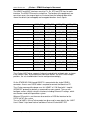
µTasker – STM32 Developer’s Document
The USART and UART interfaces consist of Tx, Rx, RTS and CTS lines for each
interface. The USARTS have also a clock line. The location of the peripherals are
consistent across the range of parts as illustrated from the following table which
shows the default (not-remapped) and remapped locations for all signals.
USART1
UART1_TXD
default Port A9
USART1_REMAP Port B6
UART1_RXD
UART1_RTS
UART1_CTS
Port A10
Port A12
Port A11
-
-
UART2_RXD
UART2_RTS
UART2_CTS
default Port A2
Port A3
Port A0
Port A1
USART2_REMAP Port D5
Port D6
Port D3
Port D4
UART3_RXD
UART3_RTS
UART3_CTS
Default Port B10
Port B11
Port B14
Port B13
USART3_PARTIAL_REMAP Port C10
Port C11
Port B14
Port B13
USART3_FULLY_REMAPPED Port D8
Port D9
Port D12
Port D11
UART4
UART4_RXD
UART4_RTS
UART4_CTS
-
-
UART5_RTS
UART5_CTS
-
-
UART6_RXD
UART6_RTS
UART6_CTS
Port C7
Port G8
Port G13
Port G9
Port G12
Port G15
USART2
USART3
UART2_TXD
UART3_TXD
UART4_TXD
default Port C10
UART5
UART5_TXD
default Port C12
USART6
UART6_TXD
default Port C6
USART6_REMAP Port G14
Port B7
Port C11
UART5_RXD
Port D2
Note that not all pins and UARTs/USARTs are available on all devices
The µTasker UART driver supports 6 channels and defaults to the pin-outs as shown
in the “default” rows. By activating the alternative defines, for UARTs with multiple
positions, the set of combinations can be configured accordingly.
On the STM3210C-EVAL board USART2 is connected to the single DSUB-9
connector. A cross-over RS232 cable is required to connect the board to a PC.
The µTasker command line demo uses this USART at 115k Baud with 1 stop bit
(XON/XOFF protocol) by default as command line menu control. The user can
configure various settings using this interface, including Ethernet IP settings, which
can then be saved to the parameter system.
When an SD card in is use the menu also contains a DOS-like interface for the
FAT32 (µtFAT) file system.
The use of UARTs in the µTasker project are discussed in more detail in the “UART
User’s Guide”: http://www.utasker.com/docs/uTasker/uTaskerUART.PDF
uTaskerV1.4_Developers_Document/0.5
18/46
22.02.2012
www.uTasker.com
µTasker – STM32 Developer’s Document
6. Ethernet
Some of the STM32 devices include an Ethernet MAC supporting 10/100M operation
with either MII or RMII interface to an external PHY.
The MAC contains support for PTP (Precision Time protocol according to IEEE1588)
and also some off-loading check sum support for IPv4 and IPv6 datagrams.
When Ethernet is used the AHB clock must be at least 25MHz.
Note that it is possible to configure the port MCO to drive various clock signals,
including 25MHz. This could be used to drive the PHY clock, for instance!
6.1. STM3210C-EVAL
The STM3210C-EVAL board uses a DP83848 as external PHY. Although it could be
configured to work in RMII mode there is no 50MHz oscillator on the board as
standard and so the MII mode is used.
Problem with ETH_DMABMR
According to the user’s manual this register resets to the value 0x2101. When
working with the debugger it was found to default to 0x20101 as soon as the
module’s clocks are enabled. The bit 0x00000001 (SR) is a module reset which
means that it starts in the reset state and the user should wait for this to return to 0
before continuing. After a power on reset this tended to hang in this wait loop forever
but when stepping the code the bit would return to zero and the board would then
start correctly.
If the reset bit could be cleared (which rarely, but sometimes happens) the value in
the register after a warm reset is 0x20100 and it doesn’t hang any more during the
initialization.
The reason for this difficulty was identified as being due to a missing clock. The
jumper JP4 was set to supply the 25MHz clock to the PHY via the MCO output but
this was not driven. By setting the jumper to the position allowing the PHYs external
25MHz crystal to be used was found to solve the issue.
Since it is interesting to be able to save the PHYs external crystal a setting was made
to configure the MCO output with a 25MHz signal:
#define ETHERNET_DRIVE_PHY_25MHZ.
The PHY interrupt is connected to an IO expander input (EXP_IO8) on the
STM3210C-EVAL board. This is quite a complicated method since it requires the I2C
driver to be used to configure the IO expander (STMPE811 Address 0x88) and its
interrupt line on PB14 to be used to detect the input change. Since a second IO
expander (I2C address 0x82) is used for touch screen operation this means that any
interrupt requires reading both chips to determine which one is requesting the
interrupt and then handling either the touch screen interrupt or the PHY interrupt.
Rather than mixing the touch screen interrupt handler with the Ethernet PHY interrupt
handler the PHY interrupt was connected in addition to PC13 (removing JP1
completely).
uTaskerV1.4_Developers_Document/0.5
19/46
22.02.2012
www.uTasker.com
µTasker – STM32 Developer’s Document
6.2. STM3240G-EVAL
The Ethernet interface on this board is equivalent to that on the STM3210C-EVAL
board. It has the PHY’s interrupt line directly connected to the processor port B-14.
6.3. Checksum Offloading
Probably the most interesting feature of the Ethernet controller in the STM32 is its
capability to perform checksum offloading. By implementing IPv4 and IPv6 payload
and header checksum calculation in hardware this calculation overhead can be
removed from software, resulting in greatly improved performance, especially when
large payload lengths would otherwise need to be calculated.
#define IP_RX_CHECKSUM_OFFLOAD - When this is defined the IPv4/v6 reception
calculation is enabled. If an IPv4/IPv6 protcol frame is received it will be immediately
discarded if the EMAC flags that there was either a payload or header checksum
error. This saves the TCP/IP stack from needing to handle frames that will obviously
fail.
Furthermore the check sum calculation is removed from the IPv4, IPv6, UDP, ICMP
and TCP reception handling. Since no frames will arrive which are corrupted there is
no need to perform these checks, resulting in much fast reception frame handling.
#define IP_TX_CHECKSUM_OFFLOAD - When this is defined the EMAC transmitter
automatically inserts the IPv4/IPv6 header checksum. This means that the IP
transmission code doesn’t need to calculate the value and insert it – it can just leave
a random value at the checksum position in the buffer.
IP_TX_PAYLOAD_CHECKSUM_OFFLOAD – When this is defined also the ICMP,
UDP,and TCP checksums and pseudo headers are automatically inserted. In this
case the checksum location must be set to the value 0x0000 since it is also used as
input to the calculation. Furthermore the transmitter operation must be set to storeand-forward mode with adequate FIO length!
This option overrides the IP_TX_CHECKSUM_OFFLOAD option and both are active.
Additional software calculation can be saved when the option is enabled.
When frames of less than 60 bytes length are transmitted the Ethernet transmitter
automatically pads them with zeros.
uTaskerV1.4_Developers_Document/0.5
20/46
22.02.2012
www.uTasker.com
µTasker – STM32 Developer’s Document
7. FLASH
7.1. F1 Flash
The connectivity line devices have 2k page sizes and devices with less than 256k
Flash have 1k page sizes. When reading program code the pre-fetch buffer (2 x 64
bytes) achieves fast instruction operation since a single pre-fetch then holds multiple
instructions. The pre-fetch buffer is enabled by default.
Programming of the FLASH takes place on half-word (16 bits). Page or full FLASH
(not information block) deletion is possible with erase time of maximum 40ms in each
case. Half-word programming takes place in max. 70us.
The STM32 user’s manual doesn’t contain programming information so this needs to
be studied in the “STM32F10xxx Flash Programming Manuals”.
After a reset the FLASH programming interface is protected and can only be
accessed after performing an unlocking sequence. This consists of the writing of a
two key sequence:
0x45670123 followed by 0xcdef89ab to the FLASH_KEYR register.
All FLASH operation is self-timed using a dedicated internal clock which has a fixed
frequency and thus avoids the need for configuration and risk of false programming
times being used.
Each half-word write includes a check of the present half-word content value. A halfword value must be 0xffff (deleted) for a half-word write to be accepted. This means
that accumulative writes to half-words is not possible.
The FLASH driver can operate from FLASH meaning that pages can be erased and
half-works written in other pages when code is running from the same FLASH
module. This also means that interrupts don’t need to be blocked when FLASH
operations are performed.
7.2. F2/F4 Flash
These parts have Flash section sizes that vary in size. There are 4 initial sections of
16k size followed by a single section of 64k size and then several sections of 128k in
size, depending on the size of Flash memory in the device.
Unlike the F1 Flash the F2/F4 Flash can be programmed as bytes, half-words, long
works or 64 bit long words. However this possibility is also dependent on the power
supply used since there is a limit to the number of bits in the programming element
that can be programmed to 0 at each operation. 64 bit programming is, for example,
only possible when an external voltage of 8..9V is applied externally on the Vpp pin
and this option is therefore generally reserved for production programming rather
than in-application programming. Below 2.1V only 8 bit programming is possible.
Below 2.7V 16 or 8 bit programming is possible. 32 bit programming is only possible
when the supply range is above 2.7V.
uTaskerV1.4_Developers_Document/0.5
21/46
22.02.2012
www.uTasker.com
µTasker – STM32 Developer’s Document
It is also to be noted that all write operations must be correctly aligned and fit within a
128 bit (16 byte) line boundary. Should any of these rules not be respected the Flash
controller will signal an error.
The operation of the Flash controller is not compatible between the F1 and F2/F4
parts and some of the registers and their contents are also different.
The cpu clock frequency (HCLK) must be at least 1MHz in order to program the
internal Flash.
Programming a byte, short word or long word takes typically 16us and maximum
100us (in worst case after 100’000 programming cycles). The sector delete durations
depend on the sector size with the 16k blocks erased in typically 300ms, the 64k
block in 700ms and the 128k blocks in 1.3s each. These values are also dependent
on the supply voltage whereby the average and maximum delete times increase with
lower voltage and a worst case of 4s for a 128k block results at the lowest operation
voltage.
The Flash driver in the µTasker STM32 project uses the project configuration to know
which parts are used and also which voltage range the design is operating in.
Therefore it adapts the programming interface accordingly without the user having to
know all details and restrictions; for example, if a low voltage configuration is being
used programming will automatically take place on a byte basis rather than on a
wider operation basis when a higher supply voltage is present and the access allows
it.
When programming memory it will do it using the widest write widths possible
depending on the power supply available (eg. When limited supply range used the
widest accesses will not be made since they are not allowed), the amount of data to
be written and the alignment of the accesses. When the STM32F2/F4 parts are used
byte writes are allowed, although they are only used when needed in preference of
wider accesses, whereas only short word writes are possible when the STM32F1xx
are used. This allows increased efficiency where the capability to write bytes allows
this – see the define NO_ACCUMULATIVE_WORDS in the µFileSystem to see an
example of its implications which is set when the STM32F1xx is used but not when
the F2/F4 parts are specified.
Due to the large flash granularity in the F2/F4 parts it is advised to use
SUB_FILE_SIZE option so that the µFileSystem can store multiple files in a single
sector. This operation is discussed in the document
http://www.utasker.com/docs/STR91XF/FileSystemSTR91X.PDF
It is further recommended to position parameter blocks as used by the
µParameterSystem in the smaller sectors at the start of the flash. Typically the
second and third sectors (each 16k) are used as parameter swap blocks since the
user of larger ones would be very inefficient in terms of memory utilisation. The first
sector is used for reset vectors and possibly a boot loader and the application code
can be located to start in the fourth boot sector (0x0000c000).
uTaskerV1.4_Developers_Document/0.5
22/46
22.02.2012
www.uTasker.com
µTasker – STM32 Developer’s Document
8. External Interrupts (EXTI)
The external interrupt controller consists of a group of 16 edge detectors for port
interrupts. These can be connected to various GPIOs (EXTI0 can be connected to
one of PA0, PB0, …PG0, etc.; EXTI1 can be connected to one of PA1, PB1, …PG1,
etc.; … EXTI15 can be connected to one of PA15, PB15, …PG15, etc.;
Additional EXTI lines (16..19 in connectivity line devices or 16..18 in others) are
connected to PVD output, RTC alarm, USB wakeup and Ethernet wakeup
respectively in the STM32F1xx parts and additionally to high-speed USB and RTC
tamper and RTC wakeup when available.
This means that there is one EXTI for each possible port bit (0..15) but each port
needs to use a different bit as they are not all available together.
EXTI0..4 have their own dedicated interrupt vectors.
EXTI5..9 and EXT10..15 share vectors for several inputs
Each interrupt input can generate falling and/or rising edge interrupts – they cannot
generate level sensitive interrupts.
A difference between the control of the connection between the port input and the
EXTI edge detector between the STM32F1xx and STM32F2/4 parts is that the F1
controls this in the alternate-function I/O block and the F2/F4 in the system
configuration controller. In both cases the corresponding block also needs to be
powered on for the operation to be successful.
9. SPI FLASH
Supported – discussion to be added…
uTaskerV1.4_Developers_Document/0.5
23/46
22.02.2012
www.uTasker.com
10.
µTasker – STM32 Developer’s Document
SD Card
SC cards and micro SD cards can usually be operated in SPI or SDIO modes.
Some of the STM32 devices have SDIO controllers allowing the faster 4 bit data
mode to be used.
When the utFAT module is used in the µTasker project on the STM3210C-EVAL
board, with STM32F107 it uses the SPI mode of operation since this device has only
SPI interfaces.
When the utFAT module is used in the µTasker project on the STM3240GEVALboard, with STM32F407 it uses the SDIO mode of operation since the micro SD
card on the board is connected to this interface. Often the SDIO pin layout of the
processors are overlaid with the corresponding SPI lines so that either SDIO or SPI
can be used. In the case of the STM32F4 this is not the case since the SDIO pins are
not multiplexed with corresponding SPI pins.
F4:
The SDIO module uses the APB2 clock for its register, interrupt and DMA operation.
The SDIO interface is clocked form the ring clock (the second output from the main
PLL). When USB FS is used this clock will be set to exactly 48MHz, otherwise its
speed can be set lower.
11.
Flexible Static Memory Controller
F4:
The FSMC can interface with various memory types in 8 or 16 bit modes. The
memory types supported are SRAM, ROM NOR Flash/OneNAND Flash and PSRAM.
Also two banks for NAND flash are supported with ECC hardware.
The memory types are supported in 4 different banks of 256 MByte size each:
Bank 1 is split into 4 NOR/PSRAM regions, whereby each has its own chip select line
[0x60000000..0x6fffffff].
Banks 2 and 3 can each address one NAND Flash device each
[0x70000000..0x7fffffff and 0x80000000..0x8fffffff].
Bank 4 can be used to address a PC card device [0x90000000..0x9fffffff].
uTaskerV1.4_Developers_Document/0.5
24/46
22.02.2012
www.uTasker.com
12.
µTasker – STM32 Developer’s Document
USB Full-Speed Device
The OTG (On-The-Go) FS (Full-speed) USB controller available on most STM32
processors supports OTG, Host and Device modes of operation.
This section discusses the device mode of operation since this is a popular mode
often used in projects where a connection via USB to a PC is required.
The USB controller is USB-IF certified to USB specification revision 2.0 and the
STM32 includes a physical, meaning that only 2 pins are required for the minimal
device mode operation. These are the OTG_FS_DP and OTG_FS_DM pins.
The USB device mode of the STM32 has been integrated into the µTasker USB
module, taking advantage of the generic USB software layers. The following technical
details are useful to be aware of since they are hardware specific to the STM32 lowlevel driver:
• USB data is coordinated in 1.25k of dedicated RAM with advanced FIFO
control, where each FIFO can hold multiple packets waiting to be transferred
or treated by the processor. The allocation of the space to the various USB
endpoints for reception and transmission use is very flexible so that this can
be dimensioned optimally for a particular use.
• In device mode there is one bi-directional control endpoint 0 and up to three IN
and OUT endpoints, supporting bulk, interrupt or isochronous transfers.
• There is a shared Rx FIFO and a Tx-OUT FIFO, as well as up to four
dedicated Tx-IN FIFOs (allowing one for each of the four possible IN
endpoints).
• The device can only operate in full-speed mode and not in low-speed mode.
• The required 48MHz +/- 0.25% clock for the USB controller core is derived
from the power and clock control module from a second output from the main
PLL, known as PLL48CLK. When USB is active the PLL VCO frequency must
be a multiple of 48MHz to allow the correct USB frequency to be achieved.
The configuration value for the PLL’s second output is calculated automatically
and an error is issued when the project is compiled when either the divide
value is not allowed or when the USB clock frequency of 48MHz is not exact.
It is to be noted that the AHB frequency (HCLK) should be greater than 14.2MHz for
correct USB device operation. If the µTasker project is configured for USB device
operation a compiler error results if this constraint is not fulfilled.
It is to be further noted that the STM32F4 supports a USB based boot loader on the
OTG_FS USB controller. In order for this to be able to operate an external clock
(HSE) needs to be available with a frequency between 4MHz and 26MHz (dividable
by 1MHz).
• When the USB controller is enabled as a device it automatically connects a
pull-up resistor to the OTG_FS_DP line.
uTaskerV1.4_Developers_Document/0.5
25/46
22.02.2012
www.uTasker.com
µTasker – STM32 Developer’s Document
The following details are the result of practical work with the FS USB device in the
STM32F4:
• The first interrupt occurs when the USB cable is connected and the host
performs a USB reset. This is signaled by the OTG_FS_GINTSTS_USBRST
flag in the core interrupt register OTG_FS_GINTSTS. The reset clears all
FIFOs and prepares for the enumeration sequence.
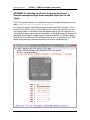
• The following figure shows the process involved when a SETUP frame is
received. The first such SETUP occurs after the USB reset in form of a
GetDescriptor (Device)
• The USB host sends the first SETUP token, which results in an interrupt since
the Rx FIFO on the control end point is no longer empty. The interrupt can be
reset before reading the FIFO content.
• The status popped from the receive FIFO show the value 0x01AC0080, which
means that 8 bytes are available and the frame is a SETUP token. The 8 bytes
of data correspond to a request for the standard device descriptor.
To complete…
uTaskerV1.4_Developers_Document/0.5
26/46
22.02.2012
www.uTasker.com
13.
µTasker – STM32 Developer’s Document
Conclusion
The purpose of this document was to give an introduction to working with the STM32
family of Cortex M3/M4 processors by introducing their basic operation and detailing
how the µTasker project makes it simple to work with them as well as move the
project between different families.
In addition to giving various information useful for practical developments quick start
guides are available in appendixes for working with the µTasker project together with
various development environments and tools.
Where appropriate, advanced chapters give insight into complex peripherals to help
better understand their practical operation and how their use is simplified by the
µTasker project and its simulator.
V0.4 17.12.2011 Provisional – in development – added Ethernet, external interrupts
and internal Flash descriptions
V0.5 22.02.2012: Added SD card, Flexible Static Memory Controller, USB-FSDevice, STM32F407-EVAL board modification (Appendix I).
uTaskerV1.4_Developers_Document/0.5
27/46
22.02.2012
www.uTasker.com
µTasker – STM32 Developer’s Document
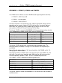
APPENDIX A - STM32F1, STM32L and STM32W
The STM32 from ST-Micro is a Cortex M3/M4 based single-chip processor family.
• STM32F1 – ARM Cortex M3
• STM32L - ultra low power
• STM32W – ARM Cortex RF
The device members are referred to as low, medium, high and XL density devices
depending on the amount of internal FLASH that they have. Low density devices
have 16k to 32k of internal FLASH, medium density devices 64k or 128k, highdensity devices 256k or 512k and XL-density 768k to 1Meg.
The internal FLASH is located at 0x08000000. Its Flash granularity (section size that
can be independently deleted) can be taken from the following table:
Flash size range
Flash granularity
Low-density
16k..32k
1k page size
Medium-density
64k..128k
1k page size
High-density
256k..512k
2k page size
768k.1M
2k page size
XL-density
The internal FLASH contains also an information block and option bytes. The
information block (0x1ffff000) is usually 2k in size and there are 16 option bytes
(0x1ffff800).
Connectivity line devices have an 18k information block at 0x1fffb000 and the XLdensity types 6k at 0x1fffe000.
Internally the FLASH is 128 bits wide. It can be accessed at up to 24MHz with zero
wait states. One wait state is required up to 48MHz and two wait states up to the
maximum operating speed of 72 MHz. SYSCLK should be equal to HCLK.
The STM32 F1 series is divided into 5 different product lines:
STM32F100xx
Value line (up to 24MHz)
STM32F101xx
Access line (up to 36MHz)
STM32F102xx
Access line (with USB) (up to 48MHz)
STM32F103xx
Performance line (up to 72MHz)
STM32F105xx/STM32F107xx
Connectivity line (up to 72MHz)
The internal SRAM is located at 0x20000000. Its size can be taken from the table of
available devices:
uTaskerV1.4_Developers_Document/0.5
28/46
22.02.2012
www.uTasker.com
µTasker – STM32 Developer’s Document
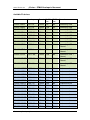
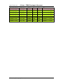
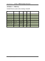
Available F1 devices
Type
Housing
Speed
STM32F105R8
LQFP 64
72MHz 64k
20k
Connectivity USB
STM32F105RB
LQFP 64
72MHz 128k
32k
Connectivity USB
STM32F105RC
LQFP 64
72MHz 256k
64k
Connectivity USB
STM32F105V8
LQFP 100
72MHz 64k
20k
Connectivity USB
STM32F105VBT
LQFP 100
72MHz 128k
32k
Connectivity USB
STM32F105VBH BGA 100
72MHz 128k
32k
Connectivity USB
STM32F105VC
LQFP 100
72MHz 256k
64k
Connectivity USB
STM32F107RB
LQFP 64
72MHz 128k
48k
Connectivity USB +
Ethernet
STM32F107RC
LQFP 64
72MHz 256k
64k
Connectivity USB +
Ethernet
STM32F107VB
LQFP 100
72MHz 128k
48k
Connectivity USB +
Ethernet
STM32F107VCT
LQFP 100
72MHz 256k
64k
Connectivity USB +
Ethernet
STM32F107VCH BGA 100
72MHz 256k
64k
Connectivity USB +
Ethernet
STM32F103ZET
LQFP 144
72MHz 512k
64k
Performance line
STM32F103ZEH
BGA 144
72MHz 512k
64k
Performance line
STM32F103ZDT
LQFP 144
72MHz 384k
64k
Performance line
STM32F103ZDH BGA 144
72MHz 384k
64k
Performance line
STM32F103ZCT
72MHz 256k
48k
Performance line
STM32F103ZCH BGA 144
72MHz 256k
48k
Performance line
STM32F103VET
72MHz 512k
64k
Performance line
STM32F103VEH BGA 100
72MHz 512k
64k
Performance line
STM32F103VDT
72MHz 384k
64k
Performance line
STM32F103VDH BGA 100
72MHz 384k
64k
Performance line
STM32F103VCT
72MHz 256k
48k
Performance line
STM32F103VCH BGA 100
72MHz 256k
48k
Performance line
STM32F103VBT
72MHz 128k
20k
Performance line
72MHz 128k
20k
Performance line
LQFP 144
LQFP 100
LQFP 100
LQFP 100
LQFP 100
STM32F103VBH BGA 100
uTaskerV1.4_Developers_Document/0.5
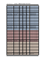
FLASH SRAM
size
size
29/46
Remarks
22.02.2012
www.uTasker.com
µTasker – STM32 Developer’s Document
STM32F103V8T
LQFP 100
72MHz 64k
20k
Performance line
STM32F103V8H
BGA 100
72MHz 64k
20k
Performance line
STM32F103TB
VFQFPN 36
72MHz 128k
20k
Performance line
STM32F103T8
VFQFPN 36
72MHz 64k
20k
Performance line
STM32F103T6
VFQFPN 36
72MHz 32k
10k
Performance line
STM32F103T4
VFQFPN 36
72MHz 16k
6k
Performance line
STM32F103RE
LQFP 64
72MHz 512k
64k
Performance line
STM32F103RD
LQFP 64
72MHz 384k
64k
Performance line
STM32F103RC
LQFP 64
72MHz 256k
48k
Performance line
STM32F103RB
LQFP 64
72MHz 128k
20k
Performance line
STM32F103R8
LQFP 64
72MHz 64k
20k
Performance line
STM32F103R6
LQFP 64
72MHz 32k
10k
Performance line
STM32F103R4
LQFP 64
72MHz 16k
6k
Performance line
STM32F103CB
LQFP 48
72MHz 128k
20k
Performance line
STM32F103C8
LQFP 48
72MHz 64k
20k
Performance line
STM32F103C6
LQFP 48
72MHz 32k
10k
Performance line
STM32F103C4
LQFP 48
72MHz 16k
6k
Performance line
STM32F102RB
LQFP 64
48MHz 128k
16k
Access line with USB
STM32F102R8
LQFP 64
48MHz 64k
10k
Access line with USB
STM32F102R6
LQFP 64
48MHz 32k
6k
Access line with USB
STM32F102R4
LQFP 64
48MHz 16k
4k
Access line with USB
STM32F102CB
LQFP 48
48MHz 128k
16k
Access line with USB
STM32F102C8
LQFP 48
48MHz 64k
10k
Access line with USB
STM32F102C6
LQFP 48
48MHz 32k
6k
Access line with USB
STM32F102C4
LQFP 48
48MHz 16k
4k
Access line with USB
STM32F101ZE
LQFP 144
36MHz 512k
48k
Access line
STM32F101ZD
LQFP 144
36MHz 384k
48k
Access line
STM32F101ZC
LQFP 144
36MHz 256k
32k
Access line
STM32F101VE
LQFP 100
36MHz 512k
48k
Access line
STM32F101VD
LQFP 100
36MHz 384k
48k
Access line
STM32F101VC
LQFP 100
36MHz 256k
32k
Access line
STM32F101VB
LQFP 100
36MHz 128k
16k
Access line
STM32F101V8
LQFP 100
36MHz 64k
10k
Access line
STM32F101TB
VFQFPN 36
36MHz 128k
16k
Access line
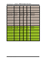
uTaskerV1.4_Developers_Document/0.5
30/46
22.02.2012
www.uTasker.com
µTasker – STM32 Developer’s Document
STM32F101T8
VFQFPN 36
36MHz 64k
10k
Access line
STM32F101T6
VFQFPN 36
36MHz 32k
6k
Access line
STM32F101T4
VFQFPN 36
36MHz 16k
4k
Access line
STM32F101RE
LQFP 64
36MHz 512k
48k
Access line
STM32F101RD
LQFP 64
36MHz 384k
48k
Access line
STM32F101RC
LQFP 64
36MHz 256k
32k
Access line
STM32F101RB
LQFP 64
36MHz 128k
16k
Access line
STM32F101R8
LQFP 64
36MHz 64k
10k
Access line
STM32F101R6
LQFP 64
36MHz 32k
6k
Access line
STM32F101R4
LQFP 64
36MHz 16k
4k
Access line
STM32F101CB
LQFP 48
36MHz 128k
16k
Access line
STM32F101C8
LQFP 48
36MHz 64k
10k
Access line
STM32F101C6
LQFP 48
36MHz 32k
6k
Access line
STM32F101C4
LQFP 48
36MHz 16k
4k
Access line
STM32F100VB
LQFP 100
24MHz 128k
8k
Value line
STM32F100V8
LQFP 100
24MHz 64k
8k
Value line
STM32F100RB
LQFP 64
24MHz 128k
8k
Value line
STM32F100R8
LQFP 64
24MHz 64k
8k
Value line
STM32F100R6
LQFP 64
24MHz 32k
4k
Value line
STM32F100R4
LQFP 64
24MHz 16k
4k
Value line
STM32F100CB
LQFP 48
24MHz 128k
8k
Value line
STM32F100C8
LQFP 48
24MHz 64k
8k
Value line
STM32F100C6
LQFP 48
24MHz 32k
4k
Value line
STM32F100C4
LQFP 48
24MHz 16k
4k
Value line
uTaskerV1.4_Developers_Document/0.5
31/46
22.02.2012
www.uTasker.com
µTasker – STM32 Developer’s Document
APPENDIX B – STM32F2xx
Available F2 devices – Cortex M3
Type
Housing
Speed
FLASH SRAM
size
size
Remarks
STM32F205RB
LQFP 64
120MHz
128k
64k
USB
STM32F205RC
LQFP 64
120MHz
256k
96k
USB
STM32F205RE
LQFP 64
120MHz
512k
128k
USB
STM32F205RF
LQFP 64
120MHz
768k
128k
USB
STM32F205RG
LQFP 64
120MHz
1M
128k
USB
STM32F205VB
LQFP 100
120MHz
128k
64k
USB
STM32F205VC
LQFP 100
120MHz
256k
96k
USB
STM32F205VE
LQFP 100
120MHz
512k
128k
USB
STM32F205VF
LQFP 100
120MHz
768k
128k
USB
STM32F205VG
LQFP 100
120MHz
1M
128k
USB
STM32F205ZC
LQFP 144
120MHz
256k
96k
USB
STM32F205ZE
LQFP 144
120MHz
512k
128k
USB
STM32F205ZF
LQFP 144
120MHz
768k
128k
USB
STM32F205ZG
LQFP 144
120MHz
1M
128k
USB
STM32F207IC
BGA 176
120MHz
256k
96k
Ethernet + 2 xUSB
STM32F207IE
BGA 176
120MHz
512k
128k
Ethernet + 2 xUSB
STM32F207IF
BGA 176
120MHz
768k
128k
Ethernet + 2 xUSB
STM32F207IG
BGA 176
120MHz
1M
128k
Ethernet + 2 xUSB
STM32F207VC
LQFP 100
120MHz
256k
128k
Ethernet + 2 xUSB
STM32F207VE
LQFP 100
120MHz
512k
128k
Ethernet + 2 xUSB
STM32F207VF
LQFP 100
120MHz
768k
128k
Ethernet + 2 xUSB
STM32F207VG
LQFP 100
120MHz
1M
128k
Ethernet + 2 xUSB
STM32F207ZC
LQFP 144
120MHz
256k
128k
Ethernet + 2 xUSB
STM32F207ZE
LQFP 144
120MHz
512k
128k
Ethernet + 2 xUSB
STM32F207ZF
LQFP 144
120MHz
768k
128k
Ethernet + 2 xUSB
STM32F207ZG
LQFP 144
120MHz
1M
128k
Ethernet + 2 xUSB
STM32F215RE
LQFP 64
120MHz
512k
128k
USB
STM32F215RG
LQFP 64
120MHz
1M
128k
USB
STM32F215VE
LQFP 100
120MHz
512k
128k
USB
uTaskerV1.4_Developers_Document/0.5
32/46
22.02.2012
www.uTasker.com
µTasker – STM32 Developer’s Document
STM32F215VG
LQFP 100
120MHz
1M
128k
USB
STM32F217IE
BGA 176
120MHz
512k
128k
Ethernet + 2 x USB
STM32F217IG
BGA 176
120MHz
1M
128k
Ethernet + 2 x USB
STM32F217VE
LQFP 100
120MHz
512k
128k
Ethernet + 2 x USB
STM32F217VG
LQFP 100
120MHz
1M
128k
Ethernet + 2 x USB
STM32F217ZE
LQFP 144
120MHz
512k
128k
Ethernet + 2 x USB
STM32F217ZG
LQFP 144
120MHz
1M
128k
Ethernet + 2 x USB
uTaskerV1.4_Developers_Document/0.5
33/46
22.02.2012
www.uTasker.com
µTasker – STM32 Developer’s Document
APPENDIX C – STM32F4xx
Available F4 devices (active at time of writing) – Cortex M4
Type
Housing
Speed
FLASH SRAM
size
size
STM32F405RG
LQFP 64
168MHz
1M
192k
STM32F407IG
BGA 176
168MHz
1M
192k
STM32F407VE
LQFP 100
168MHz
512k
192k
STM32F407VG
LQFP 100
168MHz
1M
192k
STM32F407ZG
LQFP 144
168MHz
1M
192k
STM32F415RG
LQFP 64
168MHz
1M
192k
STM32F417IG
BGA 176
168MHz
1M
192k
STM32F417VG
LQFP 100
168MHz
1M
192k
STM32F417ZG
LQFP 144
168MHz
1M
192k
uTaskerV1.4_Developers_Document/0.5
34/46
Remarks
22.02.2012
www.uTasker.com
µTasker – STM32 Developer’s Document
APPENDIX D – Building the µTasker Project in the µTasker
Simulator and generating a cross-compiled Object for the HW
Target
The µTasker project contains VisualStudio 6.0 and VisualStudio 2010 projects in the
folder \Applications\uTaskerV1.4\Simulator.
This allows the project to be build and executed with the µTasker simulator – this is
detailed in the µTasker tutorial to the STM32 devices. When the simulator runs the
same project code is executed that will later be operating on the HW target but the
simulation environment gives powerful capabilities enabling development, testing and
debugging of the majority of project code (including peripheral use) without needing
to leave the PC environment. The following screen short is an example of an STM32
device being simulated, showing the present use of ports and peripherals.
uTaskerV1.4_Developers_Document/0.5
35/46
22.02.2012
www.uTasker.com
µTasker – STM32 Developer’s Document
For users of the GCC tool chain who don’t need to work in an DIE for the target
processor the project can be built with the cross-compiler by selecting the
VisualStudio target „Win32 uTasker STM32 plus GNU build“.
When the VisualStudio successfully builds the bat file
\Applications\uTaskerV1.4\GNU_STM32\Build_STM32.bat is executed as
a post-build step. This creates binare and hex outputs for stand-alone and boot
loadable targets based on the make file make_uTaskerV1.4_GNU_STM32 in the
same folder.
The linker script file for the stand-alone target is uTaskerSTM32.ld, which is
configured for a processor with 1M internal Flash and 192k internal SRAM. This file
can generally be used without changes since the actual project details are controlled
in the initialisation code of the µTasker project which automatically configures the
initial stack pointer to suit. The linker script’s memory dimensions simply inform the
linker how much maximum resources are available. If the user desires a warning
from the linker when too much code or variables are generated to fit into the physical
limits imposed by the chip the SRAM and Flash sizes in the linker script file can
simply be reduced to match.
The VisualStudio console window shows the result fo the build as illustrated in the
following example (only one C-file compile step is shown to save space):
...
arm-none-eabi-gcc -mcpu=cortex-m4 -mfpu=fpv4-sp-d16 -mlittle-endian -mthumb -Wall Wstrict-prototypes -I../../uTaskerV1.4 -D _GNU -D _STM32 -g -c -Os
../../../stack/zero_config.c -o Build/zero_config.o
arm-none-eabi-gcc -mcpu=cortex-m4 -mfpu=fpv4-sp-d16 -mlittle-endian -mthumb -Wall Wstrict-prototypes -I../../uTaskerV1.4 -D _GNU -D _STM32 -g -Os -Wl,Map=uTaskerV1.4.map --no-gc-sections -nostartfiles -TuTaskerSTM32.ld -o
uTaskerV1.4.elf Build/app
lication.o Build/debug.o Build/webInterface.o Build/KeyScan.o
Build/NetworkIndicator.o Build/usb_application.o Build/STM32.o Build/MODBUS.o
Build/modbus_app.o Build/mass_storage.o Build/GLCD.o Build/LCD.o Build/eth_drv.o
Build/Driver.o Build/uMalloc
.o Build/uTasker.o Build/Tty_drv.o Build/iic_drv.o Build/USB_drv.o Build/uFile.o
Build/Watchdog.o Build/GlobalTimer.o Build/low_power.o Build/Ethernet.o Build/arp.o
Build/dhcp.o Build/dns.o Build/ftp.o Build/http.o Build/icmp.o Build/ip_utils.o
Buil
d/ip.o Build/pop3.o Build/smtp.o Build/snmp.o Build/tcp.o Build/telnet.o
Build/tftp.o Build/udp.o Build/webutils.o Build/NetBIOS.o Build/zero_config.o
arm-none-eabi-gcc -mcpu=cortex-m4 -mfpu=fpv4-sp-d16 -mlittle-endian -mthumb -Wall Wstrict-prototypes -I../../uTaskerV1.4 -D _GNU -D _STM32 -g -Os -Wl,Map=uTaskerV1.4_BM.map --no-gc-sections -nostartfiles -TuTaskerSTM32_BM.ld -o
uTaskerV1.4_BM.elf
Build/application.o Build/debug.o Build/webInterface.o Build/KeyScan.o
Build/NetworkIndicator.o Build/usb_application.o Build/STM32.o Build/MODBUS.o
Build/modbus_app.o Build/mass_storage.o Build/GLCD.o Build/LCD.o Build/eth_drv.o
Build/Driver.o Buil
d/uMalloc.o Build/uTasker.o Build/Tty_drv.o Build/iic_drv.o Build/USB_drv.o
Build/uFile.o Build/Watchdog.o Build/GlobalTimer.o Build/low_power.o
Build/Ethernet.o Build/arp.o Build/dhcp.o Build/dns.o Build/ftp.o Build/http.o
Build/icmp.o Build/ip_uti
ls.o Build/ip.o Build/pop3.o Build/smtp.o Build/snmp.o Build/tcp.o Build/telnet.o
Build/tftp.o Build/udp.o Build/webutils.o Build/NetBIOS.o Build/zero_config.o
arm-none-eabi-objcopy --only-section=.data --only-section=.init --onlysection=.text --only-section=.rodata --only-section=.vectors --output-target=ihex
uTaskerV1.4.elf uTaskerV1.4.hex
arm-none-eabi-objcopy --only-section=.data --only-section=.init --onlysection=.text --only-section=.rodata --only-section=.vectors --output-target=binary
uTaskerV1.4.elf uTaskerV1.4.bin
uTaskerV1.4_Developers_Document/0.5
36/46
22.02.2012
www.uTasker.com
µTasker – STM32 Developer’s Document
arm-none-eabi-objcopy --only-section=.data --only-section=.init --onlysection=.text --only-section=.rodata --only-section=.vectors --output-target=binary
uTaskerV1.4_BM.elf uTaskerV1.4_BM.bin
arm-none-eabi-size uTaskerV1.4.elf
text
data
bss
dec
hex filename
23501
81
432
24014
5dce uTaskerV1.4.elf
arm-none-eabi-gcc -v
Using built-in specs.
Target: arm-none-eabi
Configured with: /scratch/julian/2010q1-release-eabi-lite/src/gcc-4.42010q1/configure --build=i686-pc-linux-gnu --host=i686-mingw32 --target=arm-noneeabi --enable-threads --disable-libmudflap --disable-libssp --disable-libstdcxx-pch
--enable-extra
-sgxxlite-multilibs --with-gnu-as --with-gnu-ld --with-specs='%{O2:%{!fno-removelocal-statics: -fremove-local-statics}} %{O*:%{O|O0|O1|O2|Os:;:%{!fno-remove-localstatics: -fremove-local-statics}}}' --enable-languages=c,c++ --disable-shared -disab
le-lto --with-newlib --with-pkgversion='Sourcery G++ Lite 2010q1-188' --withbugurl=https://support.codesourcery.com/GNUToolchain/ --disable-nls -prefix=/opt/codesourcery --with-headers=yes --with-sysroot=/opt/codesourcery/armnone-eabi --with-buil
d-sysroot=/scratch/julian/2010q1-release-eabi-lite/install/host-i686-mingw32/armnone-eabi --with-libiconv-prefix=/scratch/julian/2010q1-release-eabi-lite/obj/hostlibs-2010q1-188-arm-none-eabi-i686-mingw32/usr --with-gmp=/scratch/julian/2010q1rele
ase-eabi-lite/obj/host-libs-2010q1-188-arm-none-eabi-i686-mingw32/usr --withmpfr=/scratch/julian/2010q1-release-eabi-lite/obj/host-libs-2010q1-188-arm-noneeabi-i686-mingw32/usr --with-ppl=/scratch/julian/2010q1-release-eabi-lite/obj/hostlibs-2010
q1-188-arm-none-eabi-i686-mingw32/usr --with-host-libstdcxx='-static-libgcc -Wl,Bstatic,-lstdc++,-Bdynamic -lm' --with-cloog=/scratch/julian/2010q1-release-eabilite/obj/host-libs-2010q1-188-arm-none-eabi-i686-mingw32/usr --disable-libgomp -enable
-poison-system-directories --with-build-time-tools=/scratch/julian/2010q1-releaseeabi-lite/obj/tools-i686-pc-linux-gnu-2010q1-188-arm-none-eabi-i686-mingw32/armnone-eabi/bin --with-build-time-tools=/scratch/julian/2010q1-release-eabilite/obj/tool
s-i686-pc-linux-gnu-2010q1-188-arm-none-eabi-i686-mingw32/arm-none-eabi/bin
Thread model: single
gcc version 4.4.1 (Sourcery G++ Lite 2010q1-188)
As can be seen, the size of the generated file as well as details about the compiler
version used are displayed. In the compiler flags it is also visible that the target is
being built for a Cortex M4 with FPU support (-mcpu=cortex-m4 -mfpu=fpv4sp-d16). This detail is in the make file and so the user should first ensure that the
correct target is being used by commenting the correct one in the file:
#C_FLAGS = -mcpu=cortex-m3 -mlittle-endian -mthumb -Wall -Wstrict-prototypes
C_FLAGS = -mcpu=cortex-m4 -mfpu=fpv4-sp-d16 -mlittle-endian -mthumb -Wall -Wstrictprototypes
The project will be built with maximum optimisation for size. In case the user wishes
to use different settings these can be adapted accordingly by editing the compiler flag
settings in the same make file.
OPTS
= -D _GNU -D _STM32 -g -c –Os
The resulting standalone object files uTaskerV1.4.bin and uTaskerV1.4.hex, which
are located in the GNU_STM32 directory can then be loaded to the STM32 Flash
uTaskerV1.4_Developers_Document/0.5
37/46
22.02.2012
www.uTasker.com
µTasker – STM32 Developer’s Document
either using a boot loader (depending on the chip type) of using and STLINK with the
ST-Micro “STM32 ST-LINK utility”.
The object files generated during the build process are located in
\Applications\uTaskerV1.4\GNU_STM32\Build. This directory must be
present to avoid build errors and its content can be simply deleted to cause the make
file to rebuild all files again.
The following software is available from the ST-Micro web site for working with the
ST-LINK; this is either a low cost JTAG/SWD adapter from ST-Micro or is a built in
interface in the discovery board.
• ST-LINK USB driver for Windows XP (this is the driver DLL used by the
various IDEs to communicate with the ST-LINK).
• ST-LINK firmware upgrade (this allows ST-LINK firmware updates to be made
or for checking the installed firmware version in the ST-LINK).
• STM32 ST-LINK utility (program allowing connecting to the device via STLINK, viewing memory, erasing memory and programming binary files to the
target).
To program the binary file generated by the simulator post-build step (or from simply
executing Build_STM32.bat) the STM32 ST-LINK utility can be opened.
• With the target connected to the PC via the ST-LINK cable a connection is
established to the board by clicking on the “Connect to the target”
button. A portion of the present memory content will then be displayed.
• The code in the STM32 flash can be erased by clicking the “Full chip
erase” button, after which the display will show all 0xff content at the start fo
Flash memory. (There is also an option to erase just certain sectors of the
chip in the “Target” menu).
• Open the uTaskerV1.4.bin file in the STM32 ST-LINK utility and then
“Program verify”. (This download dialog is usually opened automatically
when the binary file is opened in the program – note that the default
programming address 0x08000000 can be used).
• Once the download has successfully completed the new program can be
started by resetting the board or by commanding a system reset in the menu
“Target | MCU Core…”.
• Once experienced with the tool it can be customised in the “Target |
Automatic mode…” menu to fully automate typical task sequences.
uTaskerV1.4_Developers_Document/0.5
38/46
22.02.2012
www.uTasker.com
µTasker – STM32 Developer’s Document
APPENDIX E – Working with the µTasker Project and Rowely
CrossWorks
Rowley CrossWorks for ARM from Rowley Associates (http://www.rowley.co.uk/) is a
modern IDE based on the GCC compiler with replacement optimised libraries. It
supports the STM32 and can be used with a large number of JTAG debuggers,
including ST-LINK and ST-LINK/V2 as well as the well-known Segger JTAG
debugger and Olimex-ARM-OCD. It is available with different licensing starting with a
Personal edition, through educational up to Commercial. Also MAC (x86), Linux (x86)
and Solaris (x86) versions are available!
The CrossWorks project is called uTaskerV14.hzp and is located in the directory
\Applications\uTaskerV1.4\Rowley_STM32. It can be opened by simply
double-clicking on this file or else from the IDE by selecting “Open Solution” and
browsing to the file.
The project has two targets: THUMB Flash Debug and THUMB Flash Release.
Both of these can be loaded to Flash and debugged but the release version is
configured for highest size optimisation and the debug version with disabled
optimisation. If possible it is recommended to work with the release version since it
also includes debug information for source-level debugging, but in case of debug
difficulties the debug version can be used (GCC debugging can be more complicated
with high optimisation level enabled since the code doesn’t always match well to the
source file).
To build the project, simply execute the “Build | Build Solution” command.
The code can be loaded to the target by clicking on the “Start execution” button
(or F5), and the IDE offers powerful debug support including monitoring registers
while the target is operating as well as setting break points without needing to halt
the operation. In addition it is possible to connect to a running target and start
debugging (“Target | Attach Debugger”) without needing to restart the
processor’s operation.
The linker script file for the stand-alone target is uTaskerSTM32.ld, which is
configured for a processor with 1M internal Flash and 192k internal SRAM. This file
can generally be used without changes since the actual project details are controlled
in the initialisation code of the µTasker project which automatically configures the
initial stack pointer to suit. The linker script’s memory dimensions simply inform the
linker how much maximum resources are available. If the user desires a warning
from the linker when too much code or variables are generated to fit into the physical
limits imposed by the chip, the SRAM and Flash sizes in the linker script file can
simply be reduced to match.
It is possible to load the code to RAM instead by selecting the RAM placement rather
than Flash placement [Click on the project in the project explorer and use the context
menu – right click – to select “Placement | RAM”].
The SRAM target is possible only when there is enough SRAM to hold the code,
variables, heap and stack required for the project to run.
uTaskerV1.4_Developers_Document/0.5
39/46
22.02.2012
www.uTasker.com
µTasker – STM32 Developer’s Document
When working with the STM32F2xx or STM32F4xx the arm-unknown-eabi tool
chain should be used instead of the arm-unknown-elf tool chain. This is
configured in the target properties under “Code Generation Options | GCC
target”
-
arm-unknown.elf is used for STM32F1xx
-
arm-unknown-eabi is used for STM32F2xx/STM32F4xx
Crossworks can connect using ST-LINK or ST-LINK/V2 (ST-LINK can actually
connect to both types but ST-LINK/V2 can only connect to V2 versions of the STLINK). Beware that the JTAG properties of these targets can be set to either
JTAG or SWD; when using the discovery board with SWD this option must be
set accordingly.
Note that the USB driver for the ST-LINK is not included in the Crossworks setup and
should be installed separately. This can be obtained from the ST-Micro web site and
is called “ST-LINK USB driver for Windows XP”. The location of
STLinkUSBDriver.dll needs to be entered in the properties of the STLINK target
under ST-LINK DLL File.
Finally, the target processor should match the one used in the hardware, which can
be set by clicking on the project in the project explorer and using the context menu –
right click – to select “Target Processor” from the drop down list that appears.
uTaskerV1.4_Developers_Document/0.5
40/46
22.02.2012
www.uTasker.com
µTasker – STM32 Developer’s Document
APPENDIX F – Working with the µTasker Project and Atollic
TrueSTUDIO
Atollic TrueSTUDIO is an Eclipe based IDE using the GCC compiler. It has various
plug-ins that can be added to it to extend the functionality of the environment for
professional users – see http://www.atollic.com/ Atollic TrueStudio is available as a
version for the ST Microprocessors or as a general version for ARM. A LITE version
allows users to experiment with real projects before upgrading to the professional
version with extended features and support. The professional version support a large
range of debuggers but the LITE version is restricted to the ST-LINK and Segger JLink.
The µTasker project includes an Atollic project that can be simply imported into the
Atollic IDE and immediately used real work:
1) Start Atollic TrueSTUDIO and go to the C/C++ perspective (a new or existing
workspace can be selected if asked for).
2) If no other projects have been created or imported the Project Explorer will be
empty. With the mouse in the Project Explorer area open the content menu
(right mouse click) and select “Import…”. When the dialog appears expand
the “General” folder by clicking the arrow just before it and then select
“Existing projects into Workspace” and click on the “Next>” button
at the bottom of the dialog.
3) In the next dialog step enter the path to the µTasker project on the PC next to
“Select root directory:”. This can be performed by using the
“Browser” button and searching for the location. When selected, the location
will appear in the “Projects” window in the dialog with a tick in front of it,
indicating that it is a valid project.
Note that there is a check box below the project window with the title “Copy
Projects into workspace”. This can be left unchecked so that the
project files are not physically copied into the workspace.
Finally click on the “Finish” button at the bottom of the dialog.
4) The uTaskerV1.4 project will now be visible as a folder in the Project Explorer.
It has a small ‘c’ on the folder indicating that it is an active project. Atollic
TrueSTUDIO will immediately build the new project, which can be seen if the
“Console” window is activated.
By expanding the project directory in the Project Explorer window the
complete project structure can be seen and files edited after opening them
with a double click on them.
Under “Project | Properties” the settings can be viewed whereby the target is
fixed for the STM32F2xx/STMF4xx if the LITE version is used.
The linker script file for the stand-alone target is stm32_flash.ld (located in
\Applications\uTaskerV1.4\Atollic), which is configured for a processor
with 1M internal Flash and 192k internal SRAM. This file can generally be used
without changes since the actual project details are controlled in the initialisation
uTaskerV1.4_Developers_Document/0.5
41/46
22.02.2012
www.uTasker.com
µTasker – STM32 Developer’s Document
code of the µTasker project which automatically configures the initial stack pointer to
suit. The linker script’s memory dimensions simply inform the linker how much
maximum resources are available. If the user desires a warning from the linker when
too much code or variables are generated to fit into the physical limits imposed by the
chip, the SRAM and Flash sizes in the linker script file can simply be reduced to
match.
The generated object file can be loaded to the HW target by clicking on the “Debug
uTaskerV1.4” button (green beetle picture). To ensure that the debugger is
correctly setup to match the one used before doing this click on the µTasker project
folder in the Project Explorer and open the context menu (right mouse click) and
select “Debug As | Debug Configurations”. In the dialog window that opens
select the JTAG Probe from the drop-down list that appears. When doing this also
check that the Interface is correctly set to either SWD or JTAG depending on the
board used (Discovery boards use SWD). Accept the changes and click on the
“Debug” button at the bottom of the dialog to start the debug session; the code will be
loaded to the board and the Debug perspective opens.
After changes have been made to the code the project can be built by executing
“Project | Build Project” or clicking on the button with the picture of a
hammer.
uTaskerV1.4_Developers_Document/0.5
42/46
22.02.2012
www.uTasker.com
µTasker – STM32 Developer’s Document
APPENDIX G – Working with the µTasker Project and IAR
IAR Embedded Workbench for ARM is a well know IDE. It supports a large amount of
ARM chip manufacturers and device families and also a wide range of JTAG
debuggers. Its ARM compiler usually generates better code densities that most other
ARM compilers.
The IAR project workspace is called uTaskerV1.4.eww and is located
in the directory \Applications\uTaskerV1.4\IAR6_STM32. IAR Embedded
Workbench can be started by double clicking on the workspace file or by opening the
workspace in the IDE itself.
There are two build targets: uTaskerV1.4 - Debug STM32 and uTaskerV1.4 –
Release STM32. Both are compiled with highest optimisation for size; the release
target runs from Flash and the debug target from SRAM. The SRAM target is
possible only when there is enough SRAM to hold the code, variables, heap and
stack required for the project to run. Generally it is not necessary to work with
reduced optimisation levels when debugging in IAR since the code can usually still
be stepped at the source level with little difficulty.
The linker script file for the stand-alone target is STM32_Flash.icf, which is
configured for a processor with 1M internal Flash and 192k internal SRAM. This file
can generally be used without changes since the actual project details are controlled
in the initialisation code of the µTasker project which automatically configures the
initial stack pointer to suit. The linker script’s memory dimensions simply inform the
linker how much maximum resources are available. If the user desires a warning
from the linker when too much code or variables are generated to fit into the physical
limits imposed by the chip the SRAM and Flash sizes in the linker script file can
simply be reduced to match. When working from SRAM the linker script file used is
STM32_RAM.icf; both linker script files are located in the directory
\Applications\uTaskerV1.4\IAR6_STM32\settings.
The project is built by clicking on the “make” button and the code is loaded to the
target by clicking on the “Download and Debug” button. When the project to be
debugged is already loaded into Flash the “Debug without Downloading” is a
practical way to debug it without needing to load the code.
When the target processor is changed the new processor type can be selected by
clicking on the µTasker project displayed in the Workspace (file explorer in IAR
Embedded Workbench) and selecting the context menu with right mouse click. Then
the project’s options are opened by executing “Options…”. In the “General
Options” category, the device type can be selected from the drop down list to suit
and the FPU option enabled if the device has an FPU.
When selecting the debugger make sure that the debugger’s option is correctly set
between JTAG and SWD – the Discovery boards require SWD.
uTaskerV1.4_Developers_Document/0.5
43/46
22.02.2012
www.uTasker.com
µTasker – STM32 Developer’s Document
APPENDIX H – Working with the µTasker Project and Keil uVision
Keil is an ARM-owned company and the uVision IDE a well-known development
environment supporting a wide range of ARM manufacturers and device families as
well as various JTAG debuggers.
The uVision project is called uTaskerV1.4.uvproj and is located in the directory
\Applications\uTaskerV1.4\uVision_STM32. The uVision project can be
opened by double clicking on this file or else by opening the project file in the IDE
itself.
The project is built by clicking on the “Build” button (or using F7) and the code is
loaded to the target using the “Start/Stop Debug Session” button (or Ctrl + F5).
The Keil project doesn’t contain a linker script file since the memory settings are
taken from the target dialog, which means that the exact device selected
automatically selects the internal memory range used. The user should however
ensure that the start of the SRAM is set to 0x20000200 rather than 0x200000000
since the µTasker project uses the start of SRAM for interrupt vectors.
When changing the settings to build for different STM32 parts there are three things
that need to be adjusted appropriately (the options dialog can be opened by using
ALT + F7):
-
Select the device that is to be used in the “Device” register.
-
Move then to the Target register and adjust the “Xtal (MHz)“ setting to
match the board’s clock (this is however optional).
-
In the “Read/Write memory areas“ set the start of SRAM (IRAM1) to
0x20000200 as described above.
uTaskerV1.4_Developers_Document/0.5
44/46
22.02.2012
www.uTasker.com
µTasker – STM32 Developer’s Document
APPENDIX I – STM3240G-EVAL Modification to allow full Demo
Functionality
Due to conflicts between peripherals and some missing connections it can be useful
to perform some small modifications to this evaluation board as discussed in this
section. The modifications allow a single project using the TFT display with backlight
intensity control together with UART, Ethernet, USB and SD card, which is otherwise
not possible.
The first problem is that the SC card cannot be used at the same time as the original
UART. This is because the board supports only one UART on USART4 with RS232
transceiver and DSUB connector. The RxD line of the UASRT is multiplexed with the
D3 line of the SD card and TxD with D2 of the SD card. When the SD card is used
alone it is possible to remove JP22 so that the output of the RS232 transceiver
doesn’t disturb the SD card data bus, but to use a serial output and the SC card
together the following modification is recommended:
1) Remove JP22
2) Connect the centre pin of JP22 with pin 33 of CN2 (USART3_RXD PB-11).
This can be performed with a plug-wire between the connector pins.
3) Break the PC track to pin 13 of U17 (RS232 transceiver output) and carefully
solder a short wire from pin 13 to JP32 pin connected to the diode D2. Also
remove D2. Now connect the same JP32 pin to pin 32 of CN2 (USART3_TXD
PB-10). This can be performed with a plug-wire between the connector pins.
USART3 (default pins) can now be used for the serial connection without disturbing
SD card, Ethernet or TFT display operation.
The TFT module is equipped with a backlight driver which can control the backlight
intensity. On the processor board this is attached to +5V, which means that the
backlight intensity is maximum and cannot be controlled.
To enable the backlight control pin 23 of the TFT module connector can be removed
so that it doesn’t connect to the main board (the input will float and the backlight will
be undefined). Adding a connection from the CN3 pin 21 (PC-6) to the TFT board
(pin 23) allows the intensity to be controlled, as well as the backlight to be disabled to
turn the LCD off when not needed.
When the signal is set to ‘0’ the backlight is off and the display is dark.
When the signal is set to ‘1’ the backlight is on and the display has maximum
intensity.
Since the pin PC-3 can be multiplexed with timer 3 output (TIMER_3_FULL_REMAP)
the intensity can also be controlled with intermediate levels by setting the PWM
output of the timer. The µTasker project controls this signal by initialising it to GPIO
output with logic level ‘0’ so that the display is initially dark. Once the display has
been initialised the backlight intensity is set with a PWM value stored as parameter
(default is 95%, which is virtually full intensity). The PWM frequency is about 1.3kHz
so that there is no flickering. It is also useful to replace the capacitor C1 on the TFT
module with an equivalent leaded capacitor (or else solder just one of the SMD ends
to the board, stand the capacitor on its end and connect the second terminal with a
short piece of wire. This stops the capacitor from “buzzing” at the switching
uTaskerV1.4_Developers_Document/0.5
45/46
22.02.2012
www.uTasker.com
µTasker – STM32 Developer’s Document
frequency. Higher frequencies are not advisable since the backlight controller will
otherwise no longer operate linearly due to its speed constraints.
uTaskerV1.4_Developers_Document/0.5
46/46
22.02.2012