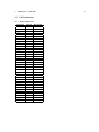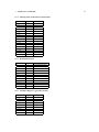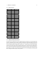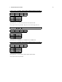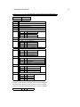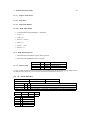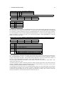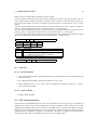
1
Yet Another Gamecube Documentation
(but one that’s worth printing)
30th May 2005
this is the result of myself pasting together various freely available documents aswell as adding some of
my own findings. have fun... additions and corrections welcome :)
THIS IS WORK IN PROGRESS! INFORMATION CONTAINED IN THIS DOCUMENT MAY
BE MISSING, INCOMPLETE OR EVEN PLAIN WRONG! NO F****N’ WARRANTY IMPLIED!
IF THE USE OF THE INFORMATION CONTAINED HERE RESULTS IN ULTRA REALISTIC
SMOKE EFFECTS, BRAIN DAMAGE OR LOSS OF PHYSICAL AND/OR MENTAL HEALTH
PLEASE DON’T COME BACK AND SAY YOU HAVEN’T BEEN WARNED! YOU SHOULDN’T
BE USING THIS IN THE FIRST PLACE!
groepaz/hitmen ([email protected])
Hitmen-Console http://www.hitmen-console.org
1
2
CONTENTS
Contents
1
2
Introductional Rant
17
1.1
Things that are in this document . . . . . . . . . . . . . . . . . . . . . . . . . . . . . . .
17
1.2
Things that are not in this document . . . . . . . . . . . . . . . . . . . . . . . . . . . . .
17
1.3
Conventions . . . . . . . . . . . . . . . . . . . . . . . . . . . . . . . . . . . . . . . . . .
18
1.4
legal Babble . . . . . . . . . . . . . . . . . . . . . . . . . . . . . . . . . . . . . . . . . .
18
Gamecube Hardware Introduction
19
2.1
enhanced PowerPC 750 Specification . . . . . . . . . . . . . . . . . . . . . . . . . . . .
19
2.2
Consumer Units . . . . . . . . . . . . . . . . . . . . . . . . . . . . . . . . . . . . . . . .
20
2.2.1
Nintendo . . . . . . . . . . . . . . . . . . . . . . . . . . . . . . . . . . . . . . .
20
2.2.1.1
HW1 . . . . . . . . . . . . . . . . . . . . . . . . . . . . . . . . . . . .
20
2.2.1.2
HW2 . . . . . . . . . . . . . . . . . . . . . . . . . . . . . . . . . . . .
20
2.2.1.3
HW2 ’second edition’ . . . . . . . . . . . . . . . . . . . . . . . . . . .
20
2.2.1.4
HW2 ’third edition’ . . . . . . . . . . . . . . . . . . . . . . . . . . . .
20
Panasonic Q . . . . . . . . . . . . . . . . . . . . . . . . . . . . . . . . . . . . .
20
2.3
Development Units . . . . . . . . . . . . . . . . . . . . . . . . . . . . . . . . . . . . . .
20
2.4
Hardware Parts List . . . . . . . . . . . . . . . . . . . . . . . . . . . . . . . . . . . . . .
20
2.4.1
Connectors . . . . . . . . . . . . . . . . . . . . . . . . . . . . . . . . . . . . . .
21
2.4.1.1
Memory Card Slots (P4,P5) . . . . . . . . . . . . . . . . . . . . . . . .
21
2.4.1.2
High-speed Port (P8) . . . . . . . . . . . . . . . . . . . . . . . . . . .
21
2.4.1.3
SDRAM/Parallel Port (P10) . . . . . . . . . . . . . . . . . . . . . . . .
22
2.4.1.4
BBA/Modem Connector (P6) . . . . . . . . . . . . . . . . . . . . . . .
22
2.4.1.5
DVD Interface Connector (P9) . . . . . . . . . . . . . . . . . . . . . .
23
2.4.1.6
Power Supply Connector (P1) . . . . . . . . . . . . . . . . . . . . . . .
24
Semi-Conductors . . . . . . . . . . . . . . . . . . . . . . . . . . . . . . . . . . .
24
2.4.2.1
IPL (U10) . . . . . . . . . . . . . . . . . . . . . . . . . . . . . . . . .
25
2.5
Details on the motherboard buses . . . . . . . . . . . . . . . . . . . . . . . . . . . . . . .
25
2.6
Details on the Macronix (MX) Chips . . . . . . . . . . . . . . . . . . . . . . . . . . . . .
25
2.7
DVD Protection . . . . . . . . . . . . . . . . . . . . . . . . . . . . . . . . . . . . . . . .
25
2.7.1
Filesystem . . . . . . . . . . . . . . . . . . . . . . . . . . . . . . . . . . . . . .
25
2.7.2
Barcode . . . . . . . . . . . . . . . . . . . . . . . . . . . . . . . . . . . . . . . .
25
2.7.3
Encryption . . . . . . . . . . . . . . . . . . . . . . . . . . . . . . . . . . . . . .
26
2.7.3.1
Cyphertext algorithm . . . . . . . . . . . . . . . . . . . . . . . . . . .
26
IPL/BIOS Encryption . . . . . . . . . . . . . . . . . . . . . . . . . . . . . . . . . . . . .
26
2.8.1
Flipper decryption logic bug . . . . . . . . . . . . . . . . . . . . . . . . . . . . .
26
2.8.2
Cyphertext algorithm . . . . . . . . . . . . . . . . . . . . . . . . . . . . . . . . .
28
2.8.3
replacing the IPL . . . . . . . . . . . . . . . . . . . . . . . . . . . . . . . . . . .
28
2.2.2
2.4.2
2.8
3
CONTENTS
3
Gekko CPU Overview
29
3.1
Registers . . . . . . . . . . . . . . . . . . . . . . . . . . . . . . . . . . . . . . . . . . .
29
3.2
Calling conventions . . . . . . . . . . . . . . . . . . . . . . . . . . . . . . . . . . . . . .
29
3.3
PPC Instructions . . . . . . . . . . . . . . . . . . . . . . . . . . . . . . . . . . . . . . .
30
3.3.1
Integer Instructions . . . . . . . . . . . . . . . . . . . . . . . . . . . . . . . . . .
30
3.3.2
Floating-Point Instructions . . . . . . . . . . . . . . . . . . . . . . . . . . . . . .
32
3.3.3
Integer Load and Store Instructions . . . . . . . . . . . . . . . . . . . . . . . . .
33
3.3.4
Floating-Point Load and Store Instructions . . . . . . . . . . . . . . . . . . . . .
34
3.3.5
Branch Instructions . . . . . . . . . . . . . . . . . . . . . . . . . . . . . . . . . .
34
3.3.6
Condition Register Logical Instructions . . . . . . . . . . . . . . . . . . . . . . .
34
3.3.7
Misc Instructions . . . . . . . . . . . . . . . . . . . . . . . . . . . . . . . . . . .
35
additional Gekko Instructions . . . . . . . . . . . . . . . . . . . . . . . . . . . . . . . . .
35
3.4.1
FPR format in paired-single mode . . . . . . . . . . . . . . . . . . . . . . . . . .
36
3.4.2
Arithmetic Instructions . . . . . . . . . . . . . . . . . . . . . . . . . . . . . . . .
36
3.4.2.1
PS_ABS . . . . . . . . . . . . . . . . . . . . . . . . . . . . . . . . . .
36
3.4.2.2
PS_ADD . . . . . . . . . . . . . . . . . . . . . . . . . . . . . . . . . .
37
3.4.2.3
PS_CMPO0 . . . . . . . . . . . . . . . . . . . . . . . . . . . . . . . .
37
3.4.2.4
PS_CMPO1 . . . . . . . . . . . . . . . . . . . . . . . . . . . . . . . .
37
3.4.2.5
PS_CMPU0 . . . . . . . . . . . . . . . . . . . . . . . . . . . . . . . .
37
3.4.2.6
PS_CMPU1 . . . . . . . . . . . . . . . . . . . . . . . . . . . . . . . .
37
3.4.2.7
PS_DIV . . . . . . . . . . . . . . . . . . . . . . . . . . . . . . . . . .
38
3.4.2.8
PS_MERGE00 . . . . . . . . . . . . . . . . . . . . . . . . . . . . . . .
38
3.4.2.9
PS_MERGE01 . . . . . . . . . . . . . . . . . . . . . . . . . . . . . . .
38
3.4.2.10 PS_MERGE10 . . . . . . . . . . . . . . . . . . . . . . . . . . . . . . .
38
3.4.2.11 PS_MERGE11 . . . . . . . . . . . . . . . . . . . . . . . . . . . . . . .
38
3.4.2.12 PS_MR . . . . . . . . . . . . . . . . . . . . . . . . . . . . . . . . . .
38
3.4.2.13 PS_NABS . . . . . . . . . . . . . . . . . . . . . . . . . . . . . . . . .
38
3.4.2.14 PS_NEG . . . . . . . . . . . . . . . . . . . . . . . . . . . . . . . . . .
38
3.4.2.15 PS_RES . . . . . . . . . . . . . . . . . . . . . . . . . . . . . . . . . .
38
3.4.2.16 PS_RSQRTE . . . . . . . . . . . . . . . . . . . . . . . . . . . . . . . .
38
3.4.2.17 PS_SUB . . . . . . . . . . . . . . . . . . . . . . . . . . . . . . . . . .
39
3.4.2.18 PS_MADD . . . . . . . . . . . . . . . . . . . . . . . . . . . . . . . .
39
3.4.2.19 PS_MADDS0 . . . . . . . . . . . . . . . . . . . . . . . . . . . . . . .
39
3.4.2.20 PS_MADDS1 . . . . . . . . . . . . . . . . . . . . . . . . . . . . . . .
39
3.4.2.21 PS_MSUB . . . . . . . . . . . . . . . . . . . . . . . . . . . . . . . . .
39
3.4.2.22 PS_MUL . . . . . . . . . . . . . . . . . . . . . . . . . . . . . . . . . .
39
3.4.2.23 PS_MULS0 . . . . . . . . . . . . . . . . . . . . . . . . . . . . . . . .
39
3.4
4
CONTENTS
3.4.2.24 PS_MULS1 . . . . . . . . . . . . . . . . . . . . . . . . . . . . . . . .
39
3.4.2.25 PS_NMADD . . . . . . . . . . . . . . . . . . . . . . . . . . . . . . . .
39
3.4.2.26 PS_NMSUB . . . . . . . . . . . . . . . . . . . . . . . . . . . . . . . .
39
3.4.2.27 PS_SEL . . . . . . . . . . . . . . . . . . . . . . . . . . . . . . . . . .
40
3.4.2.28 PS_SUM0 . . . . . . . . . . . . . . . . . . . . . . . . . . . . . . . . .
40
3.4.2.29 PS_SUM1 . . . . . . . . . . . . . . . . . . . . . . . . . . . . . . . . .
40
Load and Store Instructions . . . . . . . . . . . . . . . . . . . . . . . . . . . . .
40
3.4.3.1
psq_lx . . . . . . . . . . . . . . . . . . . . . . . . . . . . . . . . . . .
40
3.4.3.2
psq_lux . . . . . . . . . . . . . . . . . . . . . . . . . . . . . . . . . .
40
3.4.3.3
psq_stx . . . . . . . . . . . . . . . . . . . . . . . . . . . . . . . . . . .
40
3.4.3.4
psq_stux . . . . . . . . . . . . . . . . . . . . . . . . . . . . . . . . . .
40
3.4.3.5
psq_l . . . . . . . . . . . . . . . . . . . . . . . . . . . . . . . . . . . .
40
3.4.3.6
psq_lu . . . . . . . . . . . . . . . . . . . . . . . . . . . . . . . . . . .
40
3.4.3.7
psq_st . . . . . . . . . . . . . . . . . . . . . . . . . . . . . . . . . . .
40
3.4.3.8
psq_stu . . . . . . . . . . . . . . . . . . . . . . . . . . . . . . . . . . .
40
modified floating point instructions . . . . . . . . . . . . . . . . . . . . . . . . .
41
3.4.4.1
fadds . . . . . . . . . . . . . . . . . . . . . . . . . . . . . . . . . . . .
41
3.4.4.2
fsubs . . . . . . . . . . . . . . . . . . . . . . . . . . . . . . . . . . . .
41
3.4.4.3
fmuls . . . . . . . . . . . . . . . . . . . . . . . . . . . . . . . . . . . .
41
3.4.4.4
fdivs . . . . . . . . . . . . . . . . . . . . . . . . . . . . . . . . . . . .
41
3.4.4.5
fmadds . . . . . . . . . . . . . . . . . . . . . . . . . . . . . . . . . . .
41
3.4.4.6
fmsubs . . . . . . . . . . . . . . . . . . . . . . . . . . . . . . . . . . .
41
3.4.4.7
fnmadds . . . . . . . . . . . . . . . . . . . . . . . . . . . . . . . . . .
41
3.4.4.8
fnmsubs . . . . . . . . . . . . . . . . . . . . . . . . . . . . . . . . . .
41
3.4.4.9
fres . . . . . . . . . . . . . . . . . . . . . . . . . . . . . . . . . . . . .
41
3.4.4.10 frsp . . . . . . . . . . . . . . . . . . . . . . . . . . . . . . . . . . . . .
41
3.4.4.11 fsel . . . . . . . . . . . . . . . . . . . . . . . . . . . . . . . . . . . . .
41
3.4.4.12 fmr . . . . . . . . . . . . . . . . . . . . . . . . . . . . . . . . . . . . .
41
Programming Tips and additional information . . . . . . . . . . . . . . . . . . . . . . . .
42
3.5.1
Machine State Register . . . . . . . . . . . . . . . . . . . . . . . . . . . . . . . .
42
3.5.2
Caches . . . . . . . . . . . . . . . . . . . . . . . . . . . . . . . . . . . . . . . .
42
3.5.3
branch unit . . . . . . . . . . . . . . . . . . . . . . . . . . . . . . . . . . . . . .
42
3.4.3
3.4.4
3.5
5
CONTENTS
4
5
Memory Map
43
4.1
Overview . . . . . . . . . . . . . . . . . . . . . . . . . . . . . . . . . . . . . . . . . . .
43
4.2
RAM usage . . . . . . . . . . . . . . . . . . . . . . . . . . . . . . . . . . . . . . . . . .
43
4.2.1
Dolphin-OS globals . . . . . . . . . . . . . . . . . . . . . . . . . . . . . . . . .
43
4.2.1.1
43
Boot Info . . . . . . . . . . . . . . . . . . . . . . . . . . . . . . . . . .
4.2.1.1.1
DVD Disc ID . . . . . . . . . . . . . . . . . . . . . . . . . .
43
4.2.1.1.2
system Info . . . . . . . . . . . . . . . . . . . . . . . . . . .
44
4.2.1.2
Debugger info . . . . . . . . . . . . . . . . . . . . . . . . . . . . . . .
44
4.2.1.3
Debugger Hook . . . . . . . . . . . . . . . . . . . . . . . . . . . . . .
44
4.2.1.4
Dolphin OS Globals . . . . . . . . . . . . . . . . . . . . . . . . . . . .
45
4.2.2
Exception Handlers . . . . . . . . . . . . . . . . . . . . . . . . . . . . . . . . . .
45
4.2.3
Dolphin-OS globals . . . . . . . . . . . . . . . . . . . . . . . . . . . . . . . . .
46
4.2.4
User Memory . . . . . . . . . . . . . . . . . . . . . . . . . . . . . . . . . . . . .
46
4.2.4.1
user program area . . . . . . . . . . . . . . . . . . . . . . . . . . . . .
46
4.2.4.2
stack area . . . . . . . . . . . . . . . . . . . . . . . . . . . . . . . . .
47
4.2.4.3
heap area . . . . . . . . . . . . . . . . . . . . . . . . . . . . . . . . . .
47
4.2.4.4
’high memory’ . . . . . . . . . . . . . . . . . . . . . . . . . . . . . . .
47
Hardware Registers
48
5.1
CP - Command Processor . . . . . . . . . . . . . . . . . . . . . . . . . . . . . . . . . . .
48
5.1.1
Token register . . . . . . . . . . . . . . . . . . . . . . . . . . . . . . . . . . . . .
49
5.2
PE - Pixel Engine . . . . . . . . . . . . . . . . . . . . . . . . . . . . . . . . . . . . . . .
50
5.3
VI - Video Interface . . . . . . . . . . . . . . . . . . . . . . . . . . . . . . . . . . . . . .
51
5.3.1
Video Modes . . . . . . . . . . . . . . . . . . . . . . . . . . . . . . . . . . . . .
61
PI - Processor Interface . . . . . . . . . . . . . . . . . . . . . . . . . . . . . . . . . . . .
62
5.4.1
Operation . . . . . . . . . . . . . . . . . . . . . . . . . . . . . . . . . . . . . . .
63
5.4.1.1
FIFO/Write Gather Pipe . . . . . . . . . . . . . . . . . . . . . . . . . .
63
5.4.1.2
Interrupts . . . . . . . . . . . . . . . . . . . . . . . . . . . . . . . . . .
63
5.4.1.3
hotreset . . . . . . . . . . . . . . . . . . . . . . . . . . . . . . . . . .
63
5.5
MI - Memory Interface . . . . . . . . . . . . . . . . . . . . . . . . . . . . . . . . . . . .
64
5.6
DSP - Digital Signal Processor Interface . . . . . . . . . . . . . . . . . . . . . . . . . . .
67
5.6.1
internal DSP Registers . . . . . . . . . . . . . . . . . . . . . . . . . . . . . . . .
70
5.6.2
Operation . . . . . . . . . . . . . . . . . . . . . . . . . . . . . . . . . . . . . . .
72
5.6.2.1
play raw audio sample . . . . . . . . . . . . . . . . . . . . . . . . . . .
72
5.6.2.2
transfer from/to ARAM . . . . . . . . . . . . . . . . . . . . . . . . . .
72
5.6.2.3
reset DSP . . . . . . . . . . . . . . . . . . . . . . . . . . . . . . . . .
73
5.6.2.4
Boot DSP Task . . . . . . . . . . . . . . . . . . . . . . . . . . . . . . .
73
5.4
6
CONTENTS
5.7
DI - DVD Interface . . . . . . . . . . . . . . . . . . . . . . . . . . . . . . . . . . . . . .
73
5.7.1
Drive Commands . . . . . . . . . . . . . . . . . . . . . . . . . . . . . . . . . . .
77
5.7.2
Drive Debug Commands . . . . . . . . . . . . . . . . . . . . . . . . . . . . . . .
78
5.7.3
Operation . . . . . . . . . . . . . . . . . . . . . . . . . . . . . . . . . . . . . . .
79
5.7.3.1
79
Drive Info (Inquiry) . . . . . . . . . . . . . . . . . . . . . . . . . . . .
5.7.3.1.1
Structure of the Drive Info Data . . . . . . . . . . . . . . . .
79
5.7.3.2
Read Disc ID / Init Disc . . . . . . . . . . . . . . . . . . . . . . . . . .
79
5.7.3.3
Read Sector . . . . . . . . . . . . . . . . . . . . . . . . . . . . . . . .
79
5.7.3.4
Seek . . . . . . . . . . . . . . . . . . . . . . . . . . . . . . . . . . . .
79
5.7.3.5
Request Error . . . . . . . . . . . . . . . . . . . . . . . . . . . . . . .
79
5.7.3.5.1
Error Codes . . . . . . . . . . . . . . . . . . . . . . . . . . .
79
5.7.3.6
Play Audio Stream . . . . . . . . . . . . . . . . . . . . . . . . . . . . .
79
5.7.3.7
Request Audio Status . . . . . . . . . . . . . . . . . . . . . . . . . . .
80
5.7.3.8
Stop Motor . . . . . . . . . . . . . . . . . . . . . . . . . . . . . . . . .
80
5.7.3.9
DVD Audio Disable . . . . . . . . . . . . . . . . . . . . . . . . . . . .
80
5.7.3.10 DVD Audio Enable . . . . . . . . . . . . . . . . . . . . . . . . . . . .
80
DVD-ROM Subsystem . . . . . . . . . . . . . . . . . . . . . . . . . . . . . . . .
80
5.7.4.1
Memory Map . . . . . . . . . . . . . . . . . . . . . . . . . . . . . . .
80
SI - Serial Interface . . . . . . . . . . . . . . . . . . . . . . . . . . . . . . . . . . . . . .
80
5.8.1
Operation . . . . . . . . . . . . . . . . . . . . . . . . . . . . . . . . . . . . . . .
86
5.8.1.1
Serial Send Buffer . . . . . . . . . . . . . . . . . . . . . . . . . . . . .
86
5.8.1.2
Serial Get Result . . . . . . . . . . . . . . . . . . . . . . . . . . . . . .
86
EXI - External Interface . . . . . . . . . . . . . . . . . . . . . . . . . . . . . . . . . . . .
86
5.9.1
Operation . . . . . . . . . . . . . . . . . . . . . . . . . . . . . . . . . . . . . . .
90
5.9.1.1
Initializing the EXI Bus . . . . . . . . . . . . . . . . . . . . . . . . . .
90
5.9.1.2
Selecting a Specific EXI Device on an EXI Channel . . . . . . . . . . .
90
5.9.1.3
Deselecting EXI Devices on an EXI Channel . . . . . . . . . . . . . . .
90
5.9.1.4
Performing an IMM Operation on a EXI Device . . . . . . . . . . . . .
90
5.7.4
5.8
5.9
5.9.1.5
5.9.1.4.1
IMM Read . . . . . . . . . . . . . . . . . . . . . . . . . . . .
90
5.9.1.4.2
IMM Write . . . . . . . . . . . . . . . . . . . . . . . . . . .
91
Performing a DMA Operation on a EXI Device . . . . . . . . . . . . .
91
5.9.1.5.1
DMA Read . . . . . . . . . . . . . . . . . . . . . . . . . . .
91
5.9.1.5.2
DMA Write . . . . . . . . . . . . . . . . . . . . . . . . . . .
91
Wait for EXI transfer completed . . . . . . . . . . . . . . . . . . . . .
91
5.10 AI - Audio Streaming Interface . . . . . . . . . . . . . . . . . . . . . . . . . . . . . . . .
91
5.11 GX FIFO (Graphic display lists) . . . . . . . . . . . . . . . . . . . . . . . . . . . . . . .
93
5.11.1 internal BP registers . . . . . . . . . . . . . . . . . . . . . . . . . . . . . . . . .
93
5.9.1.6
7
CONTENTS
5.11.2 internal CP Registers . . . . . . . . . . . . . . . . . . . . . . . . . . . . . . . . . 127
5.11.3 internal XF Memory . . . . . . . . . . . . . . . . . . . . . . . . . . . . . . . . . 134
5.11.4 internal XF Registers . . . . . . . . . . . . . . . . . . . . . . . . . . . . . . . . . 135
5.11.5 GP packet description . . . . . . . . . . . . . . . . . . . . . . . . . . . . . . . . 147
5.11.5.1 Command Type . . . . . . . . . . . . . . . . . . . . . . . . . . . . . . 147
5.11.5.1.1
opcodes . . . . . . . . . . . . . . . . . . . . . . . . . . . . . 147
5.11.5.2 Drawing Commands . . . . . . . . . . . . . . . . . . . . . . . . . . . . 148
5.11.5.2.1
Quads . . . . . . . . . . . . . . . . . . . . . . . . . . . . . . 148
5.11.5.2.2
Triangles . . . . . . . . . . . . . . . . . . . . . . . . . . . . . 148
5.11.5.2.3
Trianglestrip . . . . . . . . . . . . . . . . . . . . . . . . . . . 149
5.11.5.2.4
TriangleFan . . . . . . . . . . . . . . . . . . . . . . . . . . . 149
5.11.5.2.5
Lines . . . . . . . . . . . . . . . . . . . . . . . . . . . . . . . 149
5.11.5.2.6
Linestrip . . . . . . . . . . . . . . . . . . . . . . . . . . . . . 149
5.11.5.2.7
Points . . . . . . . . . . . . . . . . . . . . . . . . . . . . . . 149
5.11.5.3 NOP - No Operation . . . . . . . . . . . . . . . . . . . . . . . . . . . . 149
5.11.5.4 CALL DL - Call Display List . . . . . . . . . . . . . . . . . . . . . . . 149
5.11.5.5 Invalidate Vertex Cache . . . . . . . . . . . . . . . . . . . . . . . . . . 149
5.11.5.6 BP command (Bypass Raster State Registers) . . . . . . . . . . . . . . 149
5.11.5.7 CP command (Command Processor Registers) . . . . . . . . . . . . . . 149
5.11.5.8 XF command (Transform Unit Registers) . . . . . . . . . . . . . . . . . 150
5.11.5.9 Indexed XF command . . . . . . . . . . . . . . . . . . . . . . . . . . . 150
6
Exception and Interrupt Processing
6.1
151
Hardware Exception Sources . . . . . . . . . . . . . . . . . . . . . . . . . . . . . . . . . 151
6.1.1
System Reset Interrupt . . . . . . . . . . . . . . . . . . . . . . . . . . . . . . . . 151
6.1.2
Machine Check Interrupt . . . . . . . . . . . . . . . . . . . . . . . . . . . . . . . 151
6.1.3
DSI Interrupt . . . . . . . . . . . . . . . . . . . . . . . . . . . . . . . . . . . . . 151
6.1.4
ISI Interrupt . . . . . . . . . . . . . . . . . . . . . . . . . . . . . . . . . . . . . . 151
6.1.5
External Interrupt . . . . . . . . . . . . . . . . . . . . . . . . . . . . . . . . . . . 151
6.1.5.1
Setup . . . . . . . . . . . . . . . . . . . . . . . . . . . . . . . . . . . . 151
6.1.5.2
Handling . . . . . . . . . . . . . . . . . . . . . . . . . . . . . . . . . . 152
6.1.6
Alignment Interrupt . . . . . . . . . . . . . . . . . . . . . . . . . . . . . . . . . 152
6.1.7
Program Interrupt . . . . . . . . . . . . . . . . . . . . . . . . . . . . . . . . . . . 152
6.1.8
FP unavailable Interrupt . . . . . . . . . . . . . . . . . . . . . . . . . . . . . . . 152
6.1.9
Decrementer Interrupt . . . . . . . . . . . . . . . . . . . . . . . . . . . . . . . . 152
6.1.10 System Call Interrupt . . . . . . . . . . . . . . . . . . . . . . . . . . . . . . . . . 152
6.1.11 Trace Interrupt . . . . . . . . . . . . . . . . . . . . . . . . . . . . . . . . . . . . 152
8
CONTENTS
6.1.12 Performance Monitor Interrupt . . . . . . . . . . . . . . . . . . . . . . . . . . . . 152
6.1.13 IABR Interrupt . . . . . . . . . . . . . . . . . . . . . . . . . . . . . . . . . . . . 152
6.1.14 Thermal Interrupt . . . . . . . . . . . . . . . . . . . . . . . . . . . . . . . . . . . 152
6.2
External Interrupt Sources . . . . . . . . . . . . . . . . . . . . . . . . . . . . . . . . . . 152
6.2.1
HSP - High Speed Port . . . . . . . . . . . . . . . . . . . . . . . . . . . . . . . . 152
6.2.1.1
TX Mailbox Interrupt . . . . . . . . . . . . . . . . . . . . . . . . . . . 153
6.2.1.2
RX Mailbox Interrupt . . . . . . . . . . . . . . . . . . . . . . . . . . . 153
6.2.1.3
ID Interrupt . . . . . . . . . . . . . . . . . . . . . . . . . . . . . . . . 153
6.2.2
Debug . . . . . . . . . . . . . . . . . . . . . . . . . . . . . . . . . . . . . . . . . 153
6.2.3
CP - Command Processor . . . . . . . . . . . . . . . . . . . . . . . . . . . . . . 153
6.2.3.1
6.2.3.2
6.2.4
6.2.5
6.2.6
6.2.7
setup . . . . . . . . . . . . . . . . . . . . . . . . . . . . . . . 153
6.2.3.1.2
handling . . . . . . . . . . . . . . . . . . . . . . . . . . . . . 153
FIFO overflow . . . . . . . . . . . . . . . . . . . . . . . . . . . . . . . 153
6.2.3.2.1
setup . . . . . . . . . . . . . . . . . . . . . . . . . . . . . . . 153
6.2.3.2.2
handling . . . . . . . . . . . . . . . . . . . . . . . . . . . . . 153
6.2.4.1
setup . . . . . . . . . . . . . . . . . . . . . . . . . . . . . . . . . . . . 153
6.2.4.2
handling . . . . . . . . . . . . . . . . . . . . . . . . . . . . . . . . . . 154
PE - Pixel Engine Token . . . . . . . . . . . . . . . . . . . . . . . . . . . . . . . 154
6.2.5.1
setup . . . . . . . . . . . . . . . . . . . . . . . . . . . . . . . . . . . . 154
6.2.5.2
handling . . . . . . . . . . . . . . . . . . . . . . . . . . . . . . . . . . 154
VI - Video Interface . . . . . . . . . . . . . . . . . . . . . . . . . . . . . . . . . 154
6.2.6.1
Setup . . . . . . . . . . . . . . . . . . . . . . . . . . . . . . . . . . . . 154
6.2.6.2
Handling . . . . . . . . . . . . . . . . . . . . . . . . . . . . . . . . . . 154
Memory Interface . . . . . . . . . . . . . . . . . . . . . . . . . . . . . . . . . . . 154
protection fault . . . . . . . . . . . . . . . . . . . . . . . . . . . . . . . 154
6.2.7.1.1
Setup . . . . . . . . . . . . . . . . . . . . . . . . . . . . . . 154
6.2.7.1.2
Handling . . . . . . . . . . . . . . . . . . . . . . . . . . . . . 155
DSP Interface . . . . . . . . . . . . . . . . . . . . . . . . . . . . . . . . . . . . . 155
6.2.8.1
6.2.9
6.2.3.1.1
PE - Pixel Engine Finished . . . . . . . . . . . . . . . . . . . . . . . . . . . . . . 153
6.2.7.1
6.2.8
FIFO underflow . . . . . . . . . . . . . . . . . . . . . . . . . . . . . . 153
Audio DMA finished . . . . . . . . . . . . . . . . . . . . . . . . . . . 155
6.2.8.1.1
Setup . . . . . . . . . . . . . . . . . . . . . . . . . . . . . . 155
6.2.8.1.2
Handling . . . . . . . . . . . . . . . . . . . . . . . . . . . . . 155
6.2.8.2
ARAM transfer complete . . . . . . . . . . . . . . . . . . . . . . . . . 155
6.2.8.3
DSP . . . . . . . . . . . . . . . . . . . . . . . . . . . . . . . . . . . . 155
Audio Streaming Interface . . . . . . . . . . . . . . . . . . . . . . . . . . . . . . 155
6.2.10 EXI . . . . . . . . . . . . . . . . . . . . . . . . . . . . . . . . . . . . . . . . . . 155
9
CONTENTS
6.2.10.1 DMA Transfer finished (TCINT channel 0, channel 1) . . . . . . . . . . 155
6.2.10.2 Ethernet Adapter (EXIIRQ channel 2) . . . . . . . . . . . . . . . . . . 155
6.2.10.2.1
setup . . . . . . . . . . . . . . . . . . . . . . . . . . . . . . . 155
6.2.10.2.2
handling . . . . . . . . . . . . . . . . . . . . . . . . . . . . . 156
6.2.10.3 Memory Card removed (EXTINT channel 0, channel 1) . . . . . . . . . 156
6.2.10.3.1
setup . . . . . . . . . . . . . . . . . . . . . . . . . . . . . . . 156
6.2.10.3.2
handling . . . . . . . . . . . . . . . . . . . . . . . . . . . . . 156
6.2.11 Serial Interface . . . . . . . . . . . . . . . . . . . . . . . . . . . . . . . . . . . . 156
6.2.12 DVD Interface . . . . . . . . . . . . . . . . . . . . . . . . . . . . . . . . . . . . 156
6.2.12.1 Break Complete . . . . . . . . . . . . . . . . . . . . . . . . . . . . . . 156
6.2.12.2 DMA finished . . . . . . . . . . . . . . . . . . . . . . . . . . . . . . . 156
6.2.12.3 Device Error . . . . . . . . . . . . . . . . . . . . . . . . . . . . . . . . 156
6.2.12.4 Cover State changed . . . . . . . . . . . . . . . . . . . . . . . . . . . . 156
6.2.13 Reset Button . . . . . . . . . . . . . . . . . . . . . . . . . . . . . . . . . . . . . 156
6.2.13.1 setup . . . . . . . . . . . . . . . . . . . . . . . . . . . . . . . . . . . . 156
6.2.13.2 handling . . . . . . . . . . . . . . . . . . . . . . . . . . . . . . . . . . 156
6.2.14 Error . . . . . . . . . . . . . . . . . . . . . . . . . . . . . . . . . . . . . . . . . 156
7
Video Processing
7.1
Used VI terms . . . . . . . . . . . . . . . . . . . . . . . . . . . . . . . . . . . . . . . . . 157
7.2
init VI . . . . . . . . . . . . . . . . . . . . . . . . . . . . . . . . . . . . . . . . . . . . . 157
7.2.1
8
157
Videomodes . . . . . . . . . . . . . . . . . . . . . . . . . . . . . . . . . . . . . . 157
7.3
render to XFB . . . . . . . . . . . . . . . . . . . . . . . . . . . . . . . . . . . . . . . . . 157
7.4
vertical retrace . . . . . . . . . . . . . . . . . . . . . . . . . . . . . . . . . . . . . . . . 157
7.5
set XFB Address . . . . . . . . . . . . . . . . . . . . . . . . . . . . . . . . . . . . . . . 157
3D Graphics Processing
8.1
8.2
158
basic operations . . . . . . . . . . . . . . . . . . . . . . . . . . . . . . . . . . . . . . . . 158
8.1.1
load BP Register . . . . . . . . . . . . . . . . . . . . . . . . . . . . . . . . . . . 158
8.1.2
load CP Register . . . . . . . . . . . . . . . . . . . . . . . . . . . . . . . . . . . 159
8.1.3
load XF Register . . . . . . . . . . . . . . . . . . . . . . . . . . . . . . . . . . . 159
8.1.4
load XF Register Indexed . . . . . . . . . . . . . . . . . . . . . . . . . . . . . . 159
example processing loop . . . . . . . . . . . . . . . . . . . . . . . . . . . . . . . . . . . 159
8.2.1
init GX . . . . . . . . . . . . . . . . . . . . . . . . . . . . . . . . . . . . . . . . 159
8.2.1.1
setup the fifos . . . . . . . . . . . . . . . . . . . . . . . . . . . . . . . 159
8.2.1.2
enable gx command processing . . . . . . . . . . . . . . . . . . . . . . 160
8.2.1.3
send setup frame . . . . . . . . . . . . . . . . . . . . . . . . . . . . . . 160
10
CONTENTS
8.2.1.3.1
8.2.2
begin frame . . . . . . . . . . . . . . . . . . . . . . . . . . . . . . . . . . . . . . 160
8.2.3
draw frame . . . . . . . . . . . . . . . . . . . . . . . . . . . . . . . . . . . . . . 160
8.2.4
end frame . . . . . . . . . . . . . . . . . . . . . . . . . . . . . . . . . . . . . . . 160
8.2.5
9
Videomodes . . . . . . . . . . . . . . . . . . . . . . . . . . . 160
8.2.4.1
copy EFB to XFB . . . . . . . . . . . . . . . . . . . . . . . . . . . . . 160
8.2.4.2
copy EFB to Texture . . . . . . . . . . . . . . . . . . . . . . . . . . . . 160
close GX . . . . . . . . . . . . . . . . . . . . . . . . . . . . . . . . . . . . . . . 160
Joy-Bus Devices
161
9.1
ID and Device List . . . . . . . . . . . . . . . . . . . . . . . . . . . . . . . . . . . . . . 161
9.2
standard Controller . . . . . . . . . . . . . . . . . . . . . . . . . . . . . . . . . . . . . . 162
9.3
9.2.1
Init . . . . . . . . . . . . . . . . . . . . . . . . . . . . . . . . . . . . . . . . . . 162
9.2.2
Read Controller Status . . . . . . . . . . . . . . . . . . . . . . . . . . . . . . . . 162
9.2.3
rumble Motor On . . . . . . . . . . . . . . . . . . . . . . . . . . . . . . . . . . . 163
9.2.4
rumble Motor Off . . . . . . . . . . . . . . . . . . . . . . . . . . . . . . . . . . . 163
Keyboard . . . . . . . . . . . . . . . . . . . . . . . . . . . . . . . . . . . . . . . . . . . 163
9.3.1
Types . . . . . . . . . . . . . . . . . . . . . . . . . . . . . . . . . . . . . . . . . 163
9.3.1.1
ASCII . . . . . . . . . . . . . . . . . . . . . . . . . . . . . . . . . . . 163
9.3.1.2
Datel . . . . . . . . . . . . . . . . . . . . . . . . . . . . . . . . . . . . 164
9.3.1.3
Tototek Adapter . . . . . . . . . . . . . . . . . . . . . . . . . . . . . . 164
9.3.2
Scancodes . . . . . . . . . . . . . . . . . . . . . . . . . . . . . . . . . . . . . . . 164
9.3.3
Init . . . . . . . . . . . . . . . . . . . . . . . . . . . . . . . . . . . . . . . . . . 165
9.3.4
Read Keyboard . . . . . . . . . . . . . . . . . . . . . . . . . . . . . . . . . . . . 165
9.4
GBA . . . . . . . . . . . . . . . . . . . . . . . . . . . . . . . . . . . . . . . . . . . . . . 165
9.5
Wavebird . . . . . . . . . . . . . . . . . . . . . . . . . . . . . . . . . . . . . . . . . . . 165
9.6
steering wheel . . . . . . . . . . . . . . . . . . . . . . . . . . . . . . . . . . . . . . . . . 165
9.7
DKongas . . . . . . . . . . . . . . . . . . . . . . . . . . . . . . . . . . . . . . . . . . . 165
9.7.1
9.8
Read Controller Status . . . . . . . . . . . . . . . . . . . . . . . . . . . . . . . . 166
Resident Evil4 Chainsaw . . . . . . . . . . . . . . . . . . . . . . . . . . . . . . . . . . . 166
10 EXI Devices
167
10.1 EXI Channel and Device List . . . . . . . . . . . . . . . . . . . . . . . . . . . . . . . . . 167
10.2 Retrieving the ID of an EXI Device . . . . . . . . . . . . . . . . . . . . . . . . . . . . . 167
10.3 Mask ROM . . . . . . . . . . . . . . . . . . . . . . . . . . . . . . . . . . . . . . . . . . 167
10.3.1 Memory Map (Europe/PAL) . . . . . . . . . . . . . . . . . . . . . . . . . . . . . 168
10.3.2 Memory Map (USA/NTSC) . . . . . . . . . . . . . . . . . . . . . . . . . . . . . 168
10.3.3 Memory Map (Japenese/NTSC) . . . . . . . . . . . . . . . . . . . . . . . . . . . 168
11
CONTENTS
10.3.4 Memory Map (Japenese/NTSC - Panasonic Q) . . . . . . . . . . . . . . . . . . . 168
10.3.5 Font Encoding . . . . . . . . . . . . . . . . . . . . . . . . . . . . . . . . . . . . 168
10.3.6 Font Layout . . . . . . . . . . . . . . . . . . . . . . . . . . . . . . . . . . . . . . 168
10.3.6.1 SJIS Font (ROM Font #1) . . . . . . . . . . . . . . . . . . . . . . . . . 168
10.3.6.2 ANSI Font (ROM Font #2) . . . . . . . . . . . . . . . . . . . . . . . . 168
10.3.7 Operation . . . . . . . . . . . . . . . . . . . . . . . . . . . . . . . . . . . . . . . 169
10.3.7.1 read . . . . . . . . . . . . . . . . . . . . . . . . . . . . . . . . . . . . 169
10.4 RTC (Real-Time Clock) . . . . . . . . . . . . . . . . . . . . . . . . . . . . . . . . . . . . 169
10.4.1 Operation . . . . . . . . . . . . . . . . . . . . . . . . . . . . . . . . . . . . . . . 169
10.4.1.1 read . . . . . . . . . . . . . . . . . . . . . . . . . . . . . . . . . . . . 169
10.4.1.2 write . . . . . . . . . . . . . . . . . . . . . . . . . . . . . . . . . . . . 169
10.5 SRAM . . . . . . . . . . . . . . . . . . . . . . . . . . . . . . . . . . . . . . . . . . . . . 169
10.5.1 Memory Map . . . . . . . . . . . . . . . . . . . . . . . . . . . . . . . . . . . . . 170
10.5.2 Operation . . . . . . . . . . . . . . . . . . . . . . . . . . . . . . . . . . . . . . . 170
10.5.2.1 read . . . . . . . . . . . . . . . . . . . . . . . . . . . . . . . . . . . . 170
10.5.2.2 write . . . . . . . . . . . . . . . . . . . . . . . . . . . . . . . . . . . . 170
10.5.3 Checksums . . . . . . . . . . . . . . . . . . . . . . . . . . . . . . . . . . . . . . 171
10.6 AD16 . . . . . . . . . . . . . . . . . . . . . . . . . . . . . . . . . . . . . . . . . . . . . 171
10.6.1 Operation . . . . . . . . . . . . . . . . . . . . . . . . . . . . . . . . . . . . . . . 171
10.6.1.1 init . . . . . . . . . . . . . . . . . . . . . . . . . . . . . . . . . . . . . 171
10.6.1.2 write . . . . . . . . . . . . . . . . . . . . . . . . . . . . . . . . . . . . 171
10.6.1.3 read . . . . . . . . . . . . . . . . . . . . . . . . . . . . . . . . . . . . 171
10.6.2 Trace-Step Values . . . . . . . . . . . . . . . . . . . . . . . . . . . . . . . . . . 171
10.6.2.1 BS . . . . . . . . . . . . . . . . . . . . . . . . . . . . . . . . . . . . . 171
10.6.2.2 BS2 . . . . . . . . . . . . . . . . . . . . . . . . . . . . . . . . . . . . 172
10.7 Memory Cards . . . . . . . . . . . . . . . . . . . . . . . . . . . . . . . . . . . . . . . . 172
10.7.1 Commands . . . . . . . . . . . . . . . . . . . . . . . . . . . . . . . . . . . . . . 172
10.7.2 Operation . . . . . . . . . . . . . . . . . . . . . . . . . . . . . . . . . . . . . . . 172
10.7.2.1 unlocking . . . . . . . . . . . . . . . . . . . . . . . . . . . . . . . . . 172
10.7.2.2 get ID . . . . . . . . . . . . . . . . . . . . . . . . . . . . . . . . . . . 172
10.7.2.2.1
Card IDs . . . . . . . . . . . . . . . . . . . . . . . . . . . . . 173
10.7.2.3 get Status . . . . . . . . . . . . . . . . . . . . . . . . . . . . . . . . . 173
10.7.2.3.1
Status Bits . . . . . . . . . . . . . . . . . . . . . . . . . . . . 173
10.7.2.4 clear Status . . . . . . . . . . . . . . . . . . . . . . . . . . . . . . . . . 173
10.7.2.5 read Block . . . . . . . . . . . . . . . . . . . . . . . . . . . . . . . . . 173
10.7.2.6 erase Card . . . . . . . . . . . . . . . . . . . . . . . . . . . . . . . . . 173
10.7.2.7 erase Sector . . . . . . . . . . . . . . . . . . . . . . . . . . . . . . . . 173
12
CONTENTS
10.7.2.8 write Block . . . . . . . . . . . . . . . . . . . . . . . . . . . . . . . . 174
10.8 Ethernet Adapter . . . . . . . . . . . . . . . . . . . . . . . . . . . . . . . . . . . . . . . 174
10.8.1 registers . . . . . . . . . . . . . . . . . . . . . . . . . . . . . . . . . . . . . . . . 174
10.8.2 command-registers . . . . . . . . . . . . . . . . . . . . . . . . . . . . . . . . . . 180
10.8.3 Operation . . . . . . . . . . . . . . . . . . . . . . . . . . . . . . . . . . . . . . . 181
10.8.3.1 selecting a register for reading . . . . . . . . . . . . . . . . . . . . . . . 181
10.8.3.2 selecting a register for writing . . . . . . . . . . . . . . . . . . . . . . . 181
10.8.3.3 selecting command-register for reading . . . . . . . . . . . . . . . . . . 181
10.8.3.4 selecting command-register for writing . . . . . . . . . . . . . . . . . . 181
10.8.3.5 init . . . . . . . . . . . . . . . . . . . . . . . . . . . . . . . . . . . . . 182
10.8.3.6 challenge/response calculation . . . . . . . . . . . . . . . . . . . . . . 182
10.8.3.7 send packet (outside interrupt) . . . . . . . . . . . . . . . . . . . . . . 183
10.8.3.8 poll received packets (outside interrupt) . . . . . . . . . . . . . . . . . . 183
10.8.3.9 received packet format . . . . . . . . . . . . . . . . . . . . . . . . . . . 184
10.9 UART . . . . . . . . . . . . . . . . . . . . . . . . . . . . . . . . . . . . . . . . . . . . . 184
10.10SD Cards . . . . . . . . . . . . . . . . . . . . . . . . . . . . . . . . . . . . . . . . . . . 184
10.11Viper ’Modchip’ . . . . . . . . . . . . . . . . . . . . . . . . . . . . . . . . . . . . . . . 184
10.12Ripper III GC ’Modchip’ . . . . . . . . . . . . . . . . . . . . . . . . . . . . . . . . . . . 184
10.13Qoob ’Modchip’ . . . . . . . . . . . . . . . . . . . . . . . . . . . . . . . . . . . . . . . 184
10.14NinjaMOD ’Modchip’ . . . . . . . . . . . . . . . . . . . . . . . . . . . . . . . . . . . . 184
11 HSP Devices
185
11.1 GB Player . . . . . . . . . . . . . . . . . . . . . . . . . . . . . . . . . . . . . . . . . . . 185
12 Memory Card Structure
186
12.1 Overview . . . . . . . . . . . . . . . . . . . . . . . . . . . . . . . . . . . . . . . . . . . 186
12.2 Header . . . . . . . . . . . . . . . . . . . . . . . . . . . . . . . . . . . . . . . . . . . . . 186
12.3 Directory . . . . . . . . . . . . . . . . . . . . . . . . . . . . . . . . . . . . . . . . . . . 186
12.3.1 Directory Entries . . . . . . . . . . . . . . . . . . . . . . . . . . . . . . . . . . . 187
12.3.1.1 Image Data . . . . . . . . . . . . . . . . . . . . . . . . . . . . . . . . . 188
12.3.1.1.1
Banner Image . . . . . . . . . . . . . . . . . . . . . . . . . . 188
12.3.1.1.2
Icon Image . . . . . . . . . . . . . . . . . . . . . . . . . . . 188
12.3.1.1.3
Palettes . . . . . . . . . . . . . . . . . . . . . . . . . . . . . 188
12.4 Block Allocation Map . . . . . . . . . . . . . . . . . . . . . . . . . . . . . . . . . . . . . 188
12.5 Checksums . . . . . . . . . . . . . . . . . . . . . . . . . . . . . . . . . . . . . . . . . . 189
13
CONTENTS
13 DVD Structure
190
13.1 Disk header . . . . . . . . . . . . . . . . . . . . . . . . . . . . . . . . . . . . . . . . . . 190
13.2 Disk header Information . . . . . . . . . . . . . . . . . . . . . . . . . . . . . . . . . . . 190
13.3 Apploader . . . . . . . . . . . . . . . . . . . . . . . . . . . . . . . . . . . . . . . . . . . 191
13.4 Format of the FST . . . . . . . . . . . . . . . . . . . . . . . . . . . . . . . . . . . . . . . 191
13.4.1 Format of a File Entry . . . . . . . . . . . . . . . . . . . . . . . . . . . . . . . . 191
14 general File Formats
192
14.1 BNR (Banner file format) . . . . . . . . . . . . . . . . . . . . . . . . . . . . . . . . . . . 192
14.2 DOL (Gamecube Executable) . . . . . . . . . . . . . . . . . . . . . . . . . . . . . . . . . 192
14.3 ELF (Executable and linkable Format) . . . . . . . . . . . . . . . . . . . . . . . . . . . . 192
14.4 GCB (QOOB Flash Files) . . . . . . . . . . . . . . . . . . . . . . . . . . . . . . . . . . . 193
14.5 GCM (Gamecube Disc Image) . . . . . . . . . . . . . . . . . . . . . . . . . . . . . . . . 193
14.6 GCI (Gamecube Game Save) . . . . . . . . . . . . . . . . . . . . . . . . . . . . . . . . . 193
14.7 GCP (Gamecube Memorycard Image) . . . . . . . . . . . . . . . . . . . . . . . . . . . . 193
14.8 TGC . . . . . . . . . . . . . . . . . . . . . . . . . . . . . . . . . . . . . . . . . . . . . . 193
14.8.1 Header . . . . . . . . . . . . . . . . . . . . . . . . . . . . . . . . . . . . . . . . 194
14.8.2 embedded GCM . . . . . . . . . . . . . . . . . . . . . . . . . . . . . . . . . . . 194
14.9 VGC (Viper Flash Files) . . . . . . . . . . . . . . . . . . . . . . . . . . . . . . . . . . . 194
15 Game File Formats
196
15.1 AFC (audio stream) . . . . . . . . . . . . . . . . . . . . . . . . . . . . . . . . . . . . . . 196
15.2 AST (audio stream) . . . . . . . . . . . . . . . . . . . . . . . . . . . . . . . . . . . . . . 196
15.3 ARC (RARC Archive) . . . . . . . . . . . . . . . . . . . . . . . . . . . . . . . . . . . . 196
15.3.1 Header . . . . . . . . . . . . . . . . . . . . . . . . . . . . . . . . . . . . . . . . 196
15.3.2 Nodes . . . . . . . . . . . . . . . . . . . . . . . . . . . . . . . . . . . . . . . . . 196
15.3.3 File Entries . . . . . . . . . . . . . . . . . . . . . . . . . . . . . . . . . . . . . . 197
15.4 ARC (audio stuff) . . . . . . . . . . . . . . . . . . . . . . . . . . . . . . . . . . . . . . . 197
15.5 ASN . . . . . . . . . . . . . . . . . . . . . . . . . . . . . . . . . . . . . . . . . . . . . . 197
15.6 AW ("audio wave"?) . . . . . . . . . . . . . . . . . . . . . . . . . . . . . . . . . . . . . 197
15.7 BAS ("audio script" ?) . . . . . . . . . . . . . . . . . . . . . . . . . . . . . . . . . . . . 197
15.8 BCA . . . . . . . . . . . . . . . . . . . . . . . . . . . . . . . . . . . . . . . . . . . . . . 197
15.9 BCK (animation of a .bmd skeleton) . . . . . . . . . . . . . . . . . . . . . . . . . . . . . 197
15.10BDL
. . . . . . . . . . . . . . . . . . . . . . . . . . . . . . . . . . . . . . . . . . . . . 197
15.11BFN (font) . . . . . . . . . . . . . . . . . . . . . . . . . . . . . . . . . . . . . . . . . . 197
15.12BIN (binary file) . . . . . . . . . . . . . . . . . . . . . . . . . . . . . . . . . . . . . . . 197
15.13BLO (screen layout for dialog screens) . . . . . . . . . . . . . . . . . . . . . . . . . . . . 198
14
CONTENTS
15.14BMD (3d model with texture and skeleton) . . . . . . . . . . . . . . . . . . . . . . . . . 198
15.15BMG . . . . . . . . . . . . . . . . . . . . . . . . . . . . . . . . . . . . . . . . . . . . . 198
15.16BMP (window bitmap (!)) . . . . . . . . . . . . . . . . . . . . . . . . . . . . . . . . . . 198
15.17BMT . . . . . . . . . . . . . . . . . . . . . . . . . . . . . . . . . . . . . . . . . . . . . . 198
15.18BCK ("Pack" file) . . . . . . . . . . . . . . . . . . . . . . . . . . . . . . . . . . . . . . . 198
15.19BRK
. . . . . . . . . . . . . . . . . . . . . . . . . . . . . . . . . . . . . . . . . . . . . 198
15.20BTI . . . . . . . . . . . . . . . . . . . . . . . . . . . . . . . . . . . . . . . . . . . . . . 198
15.20.1 Texture Header . . . . . . . . . . . . . . . . . . . . . . . . . . . . . . . . . . . . 199
15.21BTP . . . . . . . . . . . . . . . . . . . . . . . . . . . . . . . . . . . . . . . . . . . . . . 199
15.22BTK . . . . . . . . . . . . . . . . . . . . . . . . . . . . . . . . . . . . . . . . . . . . . . 199
15.23COL (collision triangles) . . . . . . . . . . . . . . . . . . . . . . . . . . . . . . . . . . . 199
15.24DZB . . . . . . . . . . . . . . . . . . . . . . . . . . . . . . . . . . . . . . . . . . . . . . 199
15.25H4M . . . . . . . . . . . . . . . . . . . . . . . . . . . . . . . . . . . . . . . . . . . . . . 200
15.26JPA (particle data) . . . . . . . . . . . . . . . . . . . . . . . . . . . . . . . . . . . . . . . 200
15.27JPC . . . . . . . . . . . . . . . . . . . . . . . . . . . . . . . . . . . . . . . . . . . . . . 200
15.28MTH (’Mute thp?’) . . . . . . . . . . . . . . . . . . . . . . . . . . . . . . . . . . . . . . 200
15.29PAD . . . . . . . . . . . . . . . . . . . . . . . . . . . . . . . . . . . . . . . . . . . . . . 200
15.30PRM (’Parameters?’) . . . . . . . . . . . . . . . . . . . . . . . . . . . . . . . . . . . . . 200
15.31REL (relocatable module) . . . . . . . . . . . . . . . . . . . . . . . . . . . . . . . . . . . 200
15.32SB . . . . . . . . . . . . . . . . . . . . . . . . . . . . . . . . . . . . . . . . . . . . . . . 200
15.33SZS (packed RARC Archive) . . . . . . . . . . . . . . . . . . . . . . . . . . . . . . . . . 200
15.34THP (video format) . . . . . . . . . . . . . . . . . . . . . . . . . . . . . . . . . . . . . . 200
15.34.1 Header data . . . . . . . . . . . . . . . . . . . . . . . . . . . . . . . . . . . . . . 201
15.34.2 Components structure . . . . . . . . . . . . . . . . . . . . . . . . . . . . . . . . 201
15.34.3 VideoInfo Structure . . . . . . . . . . . . . . . . . . . . . . . . . . . . . . . . . . 201
15.34.4 AudioInfo Structure . . . . . . . . . . . . . . . . . . . . . . . . . . . . . . . . . 201
15.34.5 Frame data . . . . . . . . . . . . . . . . . . . . . . . . . . . . . . . . . . . . . . 202
15.34.6 Video Frames . . . . . . . . . . . . . . . . . . . . . . . . . . . . . . . . . . . . . 202
15.34.7 Audio Frames . . . . . . . . . . . . . . . . . . . . . . . . . . . . . . . . . . . . . 202
15.35TPL (Texture Palette) . . . . . . . . . . . . . . . . . . . . . . . . . . . . . . . . . . . . . 203
15.36YMP (height map) . . . . . . . . . . . . . . . . . . . . . . . . . . . . . . . . . . . . . . 204
16 Compression Formats
205
16.1 Yay0 . . . . . . . . . . . . . . . . . . . . . . . . . . . . . . . . . . . . . . . . . . . . . . 205
16.1.1 compression . . . . . . . . . . . . . . . . . . . . . . . . . . . . . . . . . . . . . 205
16.1.2 de-compression Code . . . . . . . . . . . . . . . . . . . . . . . . . . . . . . . . . 205
16.1.3 Font Data . . . . . . . . . . . . . . . . . . . . . . . . . . . . . . . . . . . . . . . 207
16.2 Yaz0 . . . . . . . . . . . . . . . . . . . . . . . . . . . . . . . . . . . . . . . . . . . . . . 207
16.2.1 de-compression Code . . . . . . . . . . . . . . . . . . . . . . . . . . . . . . . . . 207
15
CONTENTS
17 Graphic Formats
209
17.1 YCbYCr . . . . . . . . . . . . . . . . . . . . . . . . . . . . . . . . . . . . . . . . . . . . 209
17.2 I4 (4bit indexed) . . . . . . . . . . . . . . . . . . . . . . . . . . . . . . . . . . . . . . . . 210
17.3 IA4 (4bit indexed with alpha) . . . . . . . . . . . . . . . . . . . . . . . . . . . . . . . . . 210
17.4 I8 (8bit indexed) . . . . . . . . . . . . . . . . . . . . . . . . . . . . . . . . . . . . . . . . 210
17.5 IA8 (8bit indexed with alpha) . . . . . . . . . . . . . . . . . . . . . . . . . . . . . . . . . 210
17.6 CI4 (compressed 4bit indexed) . . . . . . . . . . . . . . . . . . . . . . . . . . . . . . . . 210
17.7 CIA4 (compressed 4bit indexed with alpha) . . . . . . . . . . . . . . . . . . . . . . . . . 210
17.8 CI8 (compressed 8bit indexed) . . . . . . . . . . . . . . . . . . . . . . . . . . . . . . . . 210
17.9 CIA8 (compressed 8bit indexed with alpha) . . . . . . . . . . . . . . . . . . . . . . . . . 210
17.10RGB4A3 . . . . . . . . . . . . . . . . . . . . . . . . . . . . . . . . . . . . . . . . . . . 210
17.10.1 RGB4A3 Pixel Format . . . . . . . . . . . . . . . . . . . . . . . . . . . . . . . . 210
17.11RGB5A1 . . . . . . . . . . . . . . . . . . . . . . . . . . . . . . . . . . . . . . . . . . . 210
17.11.1 RGB5A1 Pixel Format . . . . . . . . . . . . . . . . . . . . . . . . . . . . . . . . 210
17.12RGB565 . . . . . . . . . . . . . . . . . . . . . . . . . . . . . . . . . . . . . . . . . . . . 211
17.12.1 RGB565 Pixel Format . . . . . . . . . . . . . . . . . . . . . . . . . . . . . . . . 211
17.13RGBA8 . . . . . . . . . . . . . . . . . . . . . . . . . . . . . . . . . . . . . . . . . . . . 211
17.13.1 RGBA8 Pixel Format . . . . . . . . . . . . . . . . . . . . . . . . . . . . . . . . . 211
17.14S3TC . . . . . . . . . . . . . . . . . . . . . . . . . . . . . . . . . . . . . . . . . . . . . 211
17.14.1 CMPR . . . . . . . . . . . . . . . . . . . . . . . . . . . . . . . . . . . . . . . . 212
18 Appendix
214
18.1 GCC Quick How To . . . . . . . . . . . . . . . . . . . . . . . . . . . . . . . . . . . . . 214
18.1.1 compile ASM to object: . . . . . . . . . . . . . . . . . . . . . . . . . . . . . . . 214
18.1.2 compile C to object: . . . . . . . . . . . . . . . . . . . . . . . . . . . . . . . . . 214
18.1.3 compile C++ to object: . . . . . . . . . . . . . . . . . . . . . . . . . . . . . . . . 214
18.1.4 link objects . . . . . . . . . . . . . . . . . . . . . . . . . . . . . . . . . . . . . . 214
18.1.5 remove unneeded sections (debug info etc) from object . . . . . . . . . . . . . . . 214
18.1.6 convert object to plain binary . . . . . . . . . . . . . . . . . . . . . . . . . . . . . 214
18.1.7 convert absolute address into filename/line number/function . . . . . . . . . . . . 214
18.1.8 Building a Crosscompiler . . . . . . . . . . . . . . . . . . . . . . . . . . . . . . 215
18.1.9 Linker Script . . . . . . . . . . . . . . . . . . . . . . . . . . . . . . . . . . . . . 215
18.1.10 Startup Code . . . . . . . . . . . . . . . . . . . . . . . . . . . . . . . . . . . . . 215
18.2 Boot Process Details . . . . . . . . . . . . . . . . . . . . . . . . . . . . . . . . . . . . . 215
18.2.1 BS - Bootstrap 1 . . . . . . . . . . . . . . . . . . . . . . . . . . . . . . . . . . . 215
18.2.2 BS2 - Bootstrap 2 . . . . . . . . . . . . . . . . . . . . . . . . . . . . . . . . . . . 215
18.2.2.1 short description of start() routine. . . . . . . . . . . . . . . . . . . . . 216
CONTENTS
16
18.2.2.2 IPL main() reversing . . . . . . . . . . . . . . . . . . . . . . . . . . . . 216
18.2.2.3 Map of IPL Library code . . . . . . . . . . . . . . . . . . . . . . . . . 223
18.2.3 Apploader . . . . . . . . . . . . . . . . . . . . . . . . . . . . . . . . . . . . . . . 224
18.2.4 Main DOL executable . . . . . . . . . . . . . . . . . . . . . . . . . . . . . . . . 229
18.3 Game and Maker Codes . . . . . . . . . . . . . . . . . . . . . . . . . . . . . . . . . . . . 230
18.3.1 Gamecodes . . . . . . . . . . . . . . . . . . . . . . . . . . . . . . . . . . . . . . 230
18.3.2 Game Serial ID . . . . . . . . . . . . . . . . . . . . . . . . . . . . . . . . . . . . 230
18.3.3 Makercodes . . . . . . . . . . . . . . . . . . . . . . . . . . . . . . . . . . . . . . 230
18.4 Macronix Chip IDs . . . . . . . . . . . . . . . . . . . . . . . . . . . . . . . . . . . . . . 232
18.5 chip simelarities . . . . . . . . . . . . . . . . . . . . . . . . . . . . . . . . . . . . . . . . 233
18.6 Easter Eggs . . . . . . . . . . . . . . . . . . . . . . . . . . . . . . . . . . . . . . . . . . 234
19 References
235
19.1 Sources . . . . . . . . . . . . . . . . . . . . . . . . . . . . . . . . . . . . . . . . . . . . 236
20 Credits
237
1
INTRODUCTIONAL RANT
1
17
Introductional Rant
If you don’t know what programming a machine down to the metal is all about, go away! no really, this
document is not for you! if you are seeking for advice on using existing solutions, such as SDKs or libraries,
you will find little to none information that is of any use for you and you might only become frustrated by
figuring out how little you know. If you however aren’t afraid of numbers and want to dare jumping into
the snake-pit of semi-accurate information based on guesswork done by a bunch of freaks - feel invited.
this was made to give you what you need in the most compressed and visually pleasing form possible. Stuff
that matters.
1.1
Things that are in this document
just about everything explicitly and specifically related to the gamecube hard- and software internals and
its programming. everything inside the box is subject to be documented, may it be relevant for actual
programming or not. its meant as a reference for everyone who wants to know in all possible detail what
makes this thing tick.
one more thing: please notice that this is a technical documentation which is presented for pure educational
purposes and higher learning, and not a moral lesson. i have decided against leaving out any information
since i believe that information by itself should not be crippled in any way. if you choose to abuse this
information for any kind of illegal activities (PLEASE DON’T!) so be it, but don’t bother me with it.
1.2
Things that are not in this document
several things were decided to not being put into this document because they didn’t fit into the ’technical
documentation’ type of concept. They may be documented separatly some time but not now and not here.
These things are:
Tips on Emulating the Gamecube on another Host system (this kind of information is only useful for
a very limited number of people, and additionally might be highly confusing and/or misleading for
those who are writing actual gamecube programs)
Explanation of the PSO (Phantasy Star Online) Exploit that lets you run code on the Gamecube
Explanation of the Codes used with Datels Action Replay
Instructions on using any tools that let you upload and execute code on the Gamecube, or any other
development related tools except anything related to setting up and using gcc as a cross-compiler
targeted to the gamecube.
anything related to gaming, cheat-codes and the like. (this is a tech-doc not a gaming FAQ!)
information on using the datel action replay to patch itself in order to execute code.
detailed and/or complete sourcecode, except when a formal explanation would just over-complicate
things. (this is a documentation, not a code library)
building and/or using a custom interface to connect a gamecube memory card to another host and
read/write data
anything related to playing/booting/copying pirated games (as you may have noticed, we do not
support piracy!)
some of these may be arguable, so if you think they should be here - probably along the lines of the
appendix - don’t hesitate to write the chapter in question and send it to me. i might include it if you write
it, but other than that i won’t care (there is still enough other stuff to complete).
1
18
INTRODUCTIONAL RANT
1.3
Conventions
we count bits starting from 0, the most significant bit of a byte is bit 7. when visualising a byte the
most significant bit comes first (left), and the least significant bit comes last (right).
when dealing with 16- or 32 byte values all figures are in big endian byte order. this means that the
most significant byte comes first (left), and the least significant byte comes last (right).
Please notice that the above is different to what IBM is using in their PPC documents. They have the
(to many people strange and wrong) idea of applying ’big endian’ to the order of bits and showing
them the other way around as we do in this document.
if known (from patents or other freely available sources) we use the same terminology as Nintendo
(or Macronix respectively) does, in particular we try to use the same names and abbreviations for
hardware registers, signals and the like as a weak attempt of providing consistency with other existing
documentation.
absolute memory addresses are shown as if the gamecube had been initialized by the original IPL
and address translation had not been changed. For this matter we dont use physical adresses to avoid
confusion for the majority of our readers.
code snippets are in either real or pseudo C language. any logical or arithmetic expressions outside
code snippets are loosely similar to C notation according to the following table:
Description
logical or bitwise AND
logical or bitwise OR
logical or bitwise exclusive OR
logical or bitwise NOT (inverse)
equality or assignment
addition
substraction
multiplication
division
Symbol
&
|
^
!
=
+
*
/
please notice that -outside code- we do not make a difference between logical and bitwise operations. if in doubt the operation is bitwise, it should however be clearly visible from the context.
1.4
legal Babble
Everything in this Document has been reverse-engineered from legally aquired software (Games), publicly available Patents and Documentation for the sole purpose of writing interoperable Software. This is
explicitly allowed (almost encouraged :)) by Sect. 1201 (f), Reverse Engineering exception of the DMCA.
2
GAMECUBE HARDWARE INTRODUCTION
2
19
Gamecube Hardware Introduction
The GameCube is a powerful piece of hardware. The whole system is based on the IBM PowerPC Gekko
processor and the custom ATI Flipper video system. The PowerPC Gekko processor is really just a PowerPC 750 with a few enhancements.
2.1
enhanced PowerPC 750 Specification
486 MHz internal processor clock
200 MHz 64-bit bus width to main memory (1.6 Gigabytes per second maximum)
32KB associative L1 Icache
32KB associative L1 Dcache with 16KB data scratchpad
Super-scalar microprocessor with five different execution units:
. 2 integer units, 1 FPU, and 1 load\store unit and branch unit
DMA unit servicing 16KB data scratchpad.
DMA request queue - 15-entry.
Write-gather buffer for writing graphics command lists to the video system.
Embedded 256KB 2-way set-associative L2 unified cache.
2 32-bit Integer Units (IU)
1 FPU, 32 and 64-bit bus width
The FPU supports Floating Point Paired Singles (FP/PS)
Branch Unit provides static AND dynamic branch prediction
Features Out-Of-Order execution which means that when an instruction delays because of data access, subsequent opcodes can continue to be decoded and executed.
The enhanced PowerPC Gekko processor also contains many features for minimization of processor delays
because of data accessing and for maximization of processing throughput:
Non-blocking caches
Branch prediction through use of the Branch Unit (BU)
8-way set-associative caches
256KB L2 transfer cache
Out-of-order execution capabilities
The instruction set of the PowerPC Gekko processor seems to be almost identical to the one of the PowerPC
750 processor.The only visible differences at the moment are that the PowerPC Gekko processor has a few
AltiVec\SIMD opcodes added to its final instruction set.
2
GAMECUBE HARDWARE INTRODUCTION
2.2
20
Consumer Units
2.2.1
Nintendo
2.2.1.1
HW1 HW1 was an initial, buggy version of the GameCube hardware that wasnt sold at retail.
2.2.1.2
HW2 HW2 is the first hardware that was sold in stores to the public.
2.2.1.3 HW2 ’second edition’ The second edition models are missing the "Serial Port 2" that the first
edition had. The plastic cover is still on the bottom of the cube, where the port used to be, but there’s just
a metal plate underneath it, and no connector.
2.2.1.4 HW2 ’third edition’
Digital A/V connector.
2.2.2
The third edition Gamecubes are missing both the "Serial Port 2", and the
Panasonic Q
There is a Gamecube combined with dvd-player manufactured by Panasonic called ’Panasonic-Q’. It seems
to be exactly the same as HW2 for the Gamecube part, except that the dvd drive is different.
2.3
Development Units
Nintendo provides development hardware units to official, licensed GameCube developers. There are
namely two different versions: the GDEV and the DDH hardware development kit units. These units
are the same as retail GameCube HW2 units with some changes: They have PC communications features
(either through SCSI or USB) and they have DVD emulation hardware instead of a proprietary mini-DVD
drive. GameCube development units also seem to have slower processor speeds than retail GameCubes,
this clock speed ranges from around 150MHz to 400MHz. Development GameCubes also seem to contain more RAM than retail ones, namely around 40MB. SNSystems also provides their own development
kit,authorized by Nintendo, called the TDEV. According to specifications directly from SNSystems, the
TDEV development hardware contains twice as much memory as retail GameCubes for debugging and a
direct PC<->TDEV USB connection for fast uploading of code and\or data. Finally, there is also another
proprietary development kit called the NR-Reader. NR-Reader’s contain less debugging capabilities than
the other development kits and are mostly meant for developers to efficiently get their demos\games to
beta testers or media. However, SNSystems reports that their ProDG development kit can be used with
a special USB adapter of theirs for directly sending program (debug) code to NR-Reader GameCubes.
Also, NR-Reader GameCubes contain different mini-DVD drives than retail GameCubes, but still use a
proprietary writing\reading format which is currently unknown. The DVD drives of NR-Readers can only
read special DVDs that can only be written correctly with NR-Writer hardware (which is really just a
Panasonic\Matshita SW-9501 with modified firmware). Also, the official debug development kits possibly
contain J-TAG support, which is a method for debugging hardware. If so, there is a possibility that J-TAG
support still remains in retail GameCubes as well, but this is purely hypothesis. If, in fact, retail GameCubes contain J-TAG debugging support then it should be possible for (homebrew) code to be uploaded
through a J-TAG cable) directly to a GameCube’s RAM and executed.
2.4
Hardware Parts List
"MBU" and "MBB" will be used to refer to parts on the top and bottom sides of the GameCube’s
mother-board respectively.
2
GAMECUBE HARDWARE INTRODUCTION
21
"DVDB" will be used to refer to parts on the DVD controller board.
"CB" will be used to refer to parts on the controller pad board.
2.4.1
Connectors
The are 10 different connectors on the GameCube’s mother-board. The following table contains an ID key
and a short functional description.
ID
P1
P2
P3
P4
P5
P6
P7
P8
P9
P10
2.4.1.1
2.4.1.2
Description
Motherboard Power Connector - MBB - Top Left
Digital Video Output Connector - MBU - Bottom Left
Controller Pad Board Connector - MBU - Middle Right
Memory Card Slot Connector A - MBU - Top Right
Memory Card Slot Connector B - MBU - Bottom Right
Serial Port Connector 1 - MBB - Top Right
Analog Video Output Connector - MBU - Middle Left
Serial Port Connector 2 - MBB - Top Right
Mini-DVD Drive Port Connector - MBU - Top Right
Hi-Speed Parallel Port Connector - MBB - Bottom Left
Memory Card Slots (P4,P5)
High-speed Port (P8)
pin
1
2
3
4
5
6
7
8
pin
1
2
3
4
5
6
7
8
9
10
11
12
Signal
EXTIN
GND
INT
3.3V
DO
5V
DI
3.3V
CS
Ground (Shield)
CLK
EXTOUT
Signal
3.3V
GND
INT
CLK
DO
DI
CS
Ground (Shield)
2
22
GAMECUBE HARDWARE INTRODUCTION
2.4.1.3
2.4.1.4
SDRAM/Parallel Port (P10)
BBA/Modem Connector (P6)
pin
1
2
3
4
5
6
7
8
9
10
11
12
13
14
15
16
17
18
19
20
21
22
23
24
25
26
27
28
29
30
31
32
33
34
35
36
pin
1
2
3
4
5
6
7
8
9
10
11
12
Signal
VCC
Ground
DQ0
DQ7
DQ1
DQ6
DQ2
DQ5
DQ3
DQ4
VCC
Ground
write enable
DQM
CAS
Clock
RAS
A12
CS (Chip Select)
A11
BA0
A9
BA1
A8
A10
A7
A0
A6
A1
A5
A2
A4
A3
INT
VCC
Ground
Signal
EXTIN
Ground (Shield)
INT
CLK
12V
DO
3.3V
3.3V
DI
CS
Ground
Ground
2
23
GAMECUBE HARDWARE INTRODUCTION
2.4.1.5
DVD Interface Connector (P9)
pin
1
2
3
4
5
6
7
8
9
10
11
12
13
14
15
16
17
18
19
20
21
22
23
24
25
26
27
28
29
30
31
32
Signal
AISLR (audio bus)
5V
AISD (audio bus)
5V
AISCLK (audio bus)
5V
DIHSTRB
5V
DIERRB
Ground
DIBRK
DICOVER
DIDSTBR
DIRSTB
DIDIR
Ground
DID7
Ground
DID6
Ground
DID5
Ground
DID4
Ground
DID3
Ground
DID2
MONI
DID1
MONOUT
DID0
Ground
2
24
GAMECUBE HARDWARE INTRODUCTION
2.4.1.6
2.4.2
ID
U1
U2
U3
U4
U5
U6
U7
U8
U9
U10
Power Supply Connector (P1)
pin
1
2
3
4
5
6
7
8
9
10
11
12
13
14
15
16
17
18
19
20
21
22
Signal
Ground
Ground
3.3V
3.3V
Ground
Ground
Ground
Ground
1.8V
1.8V
1.8V
1.8V
1.55V
1.55V
1.55V
Ground
Ground
Ground
Thermo detect
12V
5V
5V
Semi-Conductors
Description
Customized NEC Flipper Chip - MBU - Middle
Customized IBM PowerPC Gekko Chip - MBU - Bottom
MoSys (MS3M23B-5 A) 12MB 1-T SRAM - MBU - Top Right
MoSys (MS3M23B-5 A) 12MB 1-T SRAM - MBU - Top Right
NEC (D4891281G5 0125XU621) 16MB ARAM - MBU - Top Left
A\V Encoder (AVE N -DOL RS5C5828) - MBB - Middle Left
Amplifier? (AMP - DOL 128 124) - MBB - Top Left
MX Clock Generator (Part Number?) - MBU - Bottom Left
MX Clock Generator (Part Number?) - MBU - Bottom Right
MX RTC/IPL (8013108-M RTCN-DOL 1R6022A1)
2
GAMECUBE HARDWARE INTRODUCTION
2.4.2.1
2.5
IPL (U10)
Pin
1
2
3
4
5
6
7
8
9
10
11
12
13
14
25
Signal
Clock
CS
serial in
Ground
serial out
osc - xtal2
osc - xtal1
Details on the motherboard buses
The GameCube has three main external buses on its mother-board: the North-Bridge, the South-Bridge,
and the East-Bridge. The fastest bus is the South-Bridge which connects the two 12MB 1T-SRAM chips
to the Flipper. The South-Bridge bus has a bus-width of 64 bits, and data is exchanged through it at rates
of about 324MHz. The North-Bridge bus connects the IBM PowerPC Gekko processor to the Flipper and
is another 64 bit bus-width bus, however, it is only half as fast as the South-Bridge bus and is clocked at
around 162MHz. Finally, the East-Bridge bus connects the 16MB Audio RAM chip to the Flipper chip.
This bus only has a bus-width of 8 bits and is by far the slowest one, clocked at only 81MHz.
2.6
Details on the Macronix (MX) Chips
An outer inspection of the two MX chips does not reveal anything of much interest. Both chips are TSOP
packages containing 14 pins each. One of the chips has "CLK" inscripted on it, and the other "RTC". It
can be easily inferred that the "CLK" chip functions as some sort of a clock controller\generator and the
"RTC" chip contains the GameCube’s Real-Time Clock unit. Two of the RTC chip’s pins are connected to
an external crystal which regulates the RTC’s timing rate. Another pin is connected to a battery located on
the controller board. At least two pins are used for both VCC and GND. That leaves nine unknown pins.
The RTC MX chip also contains the GameCube’s BIOS. While 14 pins is not nearly enough for parallel
Flash ROM, EEPROM, mask ROM, etc., it is quite adequate for a serial connection.
2.7
DVD Protection
The DVD Protection is based on a custom data format on an otherwhise pretty standard dvd.
2.7.1
Filesystem
The custom Filesystem (which is described somewhere else in this Document) by itself is not related to the
actual protection mechanism. However, since it is not standard, that alone would already make it hard to
read (and create) in a regular (pc-) environment.
2.7.2
Barcode
The Barcode is used to authenticate the Disc in the Drive.
2
GAMECUBE HARDWARE INTRODUCTION
2.7.3
26
Encryption
The entire content of a Gamecube DVD is XORed with a constant cyphertext and it is transparently decrypted by the Disc-Controller when reading from the DVD.
2.7.3.1
2.8
Cyphertext algorithm todo
IPL/BIOS Encryption
if you XOR an NTSC with a PAL bios (or any other two different ones), you will notice that because they
have different sizes, there are some obviously zero encoded areas in one files, giving you plaintext in the
other one which proves:
encryption is a simple XOR with a constant ciphertext.
the key used to generate the cyphertext is the same for different bios’s
so we do the math:
given Ci = ciphertext, Cl = cleartext, K = key
encoding data goes like:
Ci1 = Cl1 ^ K
Ci2 = Cl2 ^ K
If Cl1 or Cl2 is nothing but zero, the resultant Ci is just K
decoding it would be:
Cl = Ci ^ K
for the areas where Cl is nothing but zeroes in one bios, we know K
2.8.1
Flipper decryption logic bug
The hardware decryption logic has a really nasty bug which allows us to read almost the full Cleartext (and
thus a large part of the cyphertext, by XORing it with encrypted data).
This, combined with the features of the XOR encryption makea the whole encryption useless (at least
very insecure) and implementing a new bios is a straight-forward task (provided that "high speed" (30Mhz)
programmable logic with enough memory attached to it is available.). The Bios chip, which also includes
sram and rtc (but that won’t matter here), is attached to the EXI0 bus. The Exi bus (nothing new here, just
to refresh it is an SPI-like bus. SPI is nothing complicated, just four interesting lines: CS (used mainly for
syncing, since you need a defined start point, and you can easily attach multiple devices (memory card, ...)
to the same bus with seperate CS lines), SI (aka MOSI, master out, slave in - the CPU is always master, the
IPL-chip is slave. so SI is gamecube -> device), SO (device -> gamecube, tristated when a device is not
active), and CLK (generated by the master). a transfer is basically:
- lower CS (it’s low active)
2
GAMECUBE HARDWARE INTRODUCTION
27
for every bit do:
- set SI bit
- clock
- read SO bit
then:
- put CS high again.
(the exact timing (WHEN to sample SO, clock polarity) is different for different SPI modes, and the one
descriped here is not necessarily the one used in the GC. anyway, it doesn’t matter here)
so, based on that, we can transfer n-bit messages in BOTH DIRECTIONS. technically this is implemented
with a 32bit shift register, with every clock cycle one bit is shifted out (to SI), and one bit is shifted in (to
SO). so after n clock cycles, you have n new bits in the shift register and shifted n bits out. the used protocol
on the Bus is in most cases very simple but device dependant. In the case of the IPL chip, it’s the following:
GC -> IPL
1 bit read/write (0 for read, 1 for write, the latter only valid for RTC/Sram of course)
1 unknown bit
1 bits selection (0 for ROM, 1 for RTC/Sram)
23 bits address
6 bits dummy
after that, the data transfer starts. the 6 dummy cycles are mainly to give the IPL time to read out the first
byte.
So you send 32 bits of data (the "address"), and start receiving the ROM bytes. but hey - we said the
SPI bus always transfers 2 bits per clock cycle (in marketing terms), since it’s fullduplex (in technical
terms). we transfer one bit TO the device, and one BACK. we HAVE to. there’s no way to NOT send a
bit - but it doesn’t matter, since for example the bits send from the IPL to the GC in the first 32bits are
just ignored - they would contain most probably only zeros, ones, or the bus might be tristate. it’s simply
not defined, so there’s no data to be expected. the same goes for the transfer of the data. the IPL chip sets
the correct data at the SO line, but the gamecube - well, sends dummy bits, too. normally you would send
zeros, ones, or whatever. it’s ignored by the IPL chip anyway (unless it’s a write, that would turn the whole
thing upside down) now since technically the SPI port is implemented by a shifting register of 32bit length.
after transferring 32bits, we would have to read out the new value, store it into memory, and "start the next
transfer". but what’s about CLEARING the register before? yes, they didn’t. in the next transfer, the last
32bit are shifted out as dummy bits. well, one might say, it’s just the data just shifted in, so it’s completely
uninteresting. BUT: the decryption of the loader is done in hardware. it’s a part between the SO line of
the IPL and the DI port of the shift register. (the encryption is build into the flipper, so no way to intercept
the content AFTER decryption).so because the (decrypted) data just shifted in (and stored into memory) is
shifted out again - we can get the decrypted data. if you sniff the SI line to the IPL chip, you will get a log
like this:
00 00
FF FF
xx xx
...
...
xx xx
40 00 (address written to the IPL, in this case: 0x100)
FF FF (well just dummy data)
xx xx (the data from the last 4 bytes, decrypted)
xx xx (the data from the n-1 transfer, decrypted)
so in the end you get every 32bit words except one. For every transfered block you miss 32bits of plaintext
data, but you’ll get the rest. This should be enough to decrypt huge parts of the bios, and thus recover a
large part of K.
2
GAMECUBE HARDWARE INTRODUCTION
2.8.2
28
Cyphertext algorithm
todo
2.8.3
replacing the IPL
using the above gained knowledge it is possible to create a small bootrom replacement (using the, yet incomplete, cyphertext), and get more (most) of the IPL Cleartext.
The Gekko boots from 0x100, that’s what you read in almost any ppc instruction manual - the reset vector.
well, this isn’t the complete truth - it boots from it’s exception base + 0x100. And the exception base is
normally zero, BUT, as the ppc manual states: there’s a bit in a HID (i think) register, which turns the
exception base to 0xFFF00000. and this bit is "set usually at boot time". So the processor starts to fetch
instructions at 0xFFF000100. If you read a bit further, you’ll notice that the CPU always reads 64bits at
once for code. The memory at 0xFFF00000 is mapped inside the flipper to an automated exi transfer (with
that shift register), with the decryption logic active. so the processor starts executing the decrypted instructions, reading 8 bytes at a time, of which we get 4 bytes in plain - not much, (although enough to make
some funny experiments, but that’s another topic). Luckily, the IPL itself (the cube menu) isn’t executed
this way since that wouldn’t be possible thanks to the "dumb" decryption logic The first ~0x800 bytes start
to read data out of the IPL chip and store it to memory (still using the hardware decryption logic), and
jump there. they read 1024 bytes at once. Well - now we know 1020 bytes of each transfer, enough to have
a complete block of code we can exchange (we have the ciphertext Cl^K = Ci on SO, and the plaintext
(delayed by 32bits on SI), and can XOR them to get Cl^K^Ci = K. now we can encrypt our code with K).
so now we can make a small code which just dumps the whole IPL - well, to the EXI bus or whereever you
can receive it. Now we have all Cl, and thus we can compute all K, thus we can get the complete Plaintext
of all available IPLs aswell as encode a larger custom IPL ourselves.
a small note on why you can not recover the plaintext of the original loader this way:
The decryption logic is, whatever it is, a PRNG. It generates a stream of ciphertext ("K"), which has random
properties (non-repeating, at least not in the range of some MB), but is always the same. it is incremented
with every EXI-transfer. the address is NOT used in the calculation. thus reading from 0xFFF00100 more
than one time will give you each time another result. the first time you get Ci(0)^K(0) (the correct result),
the second time you get Ci(0)^K(1) etc., i.e. wrong results. Since we never get the K(n) for odd n, i see no
chance of recovering it this way, even if we can read at 0xFFF00000+x (and we can do this if we don’t set
a specific bit to disable the logic).
3
29
GEKKO CPU OVERVIEW
3
Gekko CPU Overview
3.1
Registers
General purpose registers (r0-r31)
. r1 sp stackpointer
. r2 rtoc global pointer to _SDA2_BASE_
. r13 global pointer to _SDA_BASE_
Floating point registers (fp0-fp31)
Segment registers (sr0-sr15) - unused in regular (SDK/DolphinOS) applications
Special purpose registers (spr0-spr1023)
. spr8 (lr) - link register
. spr920 - HID2
. spr1010 - instruction breakpoint address
. spr1013 - data breakpoint address
spr920
31
24
bit(s)
2
1
0
3.2
4
r/w
23
16
HID2
15
8
7
0
description
PSE - Paired-Single load and store instructions enabled
LSQE - Paired-Single mode enabled
Calling conventions
parameters are passed in r3 (1st) r4 (2nd) and r5 (third) up to r12 (9th), further parameters are passed
through the stack.
3
GEKKO CPU OVERVIEW
3.3
PPC Instructions
3.3.1
Integer Instructions
Mnemonic
addi
addis
add
addo
subf
subfo
addic
subfic
addc
addco
subfc
subfco
adde
addeo
subfe
subfeo
addme
addmeo
subfme
subfmeo
addze
addzeo
subfze
subfzeo
neg
nego
mulli
mullw
mullwo
mulhw
mulhwu
divw
divwo
divwu
divwuo
cmpi
cmp
cmpli
cmpl
Opcode
Description
30
3
GEKKO CPU OVERVIEW
Mnemonic
andi
andis
ori
oris
xori
xoris
and
or
xor
nand
nor
eqv
andc
orc
Mnemonic
extsb
extsh
cntlzw
rlwinm
rlwnm
rlwimi
slw
srw
srawi
sraw
Opcode
Description
Opcode
Description
31
3
GEKKO CPU OVERVIEW
3.3.2
Floating-Point Instructions
Mnemonic
fadd
fadds (*)
fsub
fsubs (*)
fmul
fmuls (*)
fdiv
fdivs
fres (*)
frsqrte
fsel (*)
fmadd
fmadds (*)
fmsub
fmsubs (*)
fnmadd
fnmadds (*)
fnmsub
fnmsubs (*)
frsp (*)
fctiw
fctiwz
fcmpu
fcmpo
mffs
mcrfs
mtfsfi
mtfsf
mtfsb0
mtfsb1
fmr (*)
fneg
fabs
fnabs
Opcode
Description
(*) - modified for paired singles
32
3
GEKKO CPU OVERVIEW
3.3.3
Integer Load and Store Instructions
Mnemonic
lbz
lbzx
lbzu
lbzux
lhz
lhzx
lhzu
lhzux
lha
lhax
lhau
lhaux
lwz
lwzx
lwzu
lwzux
stb
stbx
stbu
stbux
sth
sthx
sthu
sthux
stw
stwx
stwu
stwux
lhbrx
lwbrx
sthbrx
stwbrx
lmw
stmw
lswi
lswx
stswi
stswx
Opcode
Description
33
3
GEKKO CPU OVERVIEW
3.3.4
Floating-Point Load and Store Instructions
Mnemonic
lfs
lfsx
lfsu
lfsux
lfd
lfdx
lfdu
lfdux
stfs
stfsx
stfsu
stfsux
stfd
stfdx
stfdu
stfdux
stfiwx
3.3.5
Description
Branch Instructions
Mnemonic
b
ba
bl
bla
bc
bca
bcl
bcla
bclr
bclrl
bcctr
bcctrl
3.3.6
Opcode
Opcode
Description
unconditional Jump
branch and link
Condition Register Logical Instructions
Mnemonic
crand
cror
crxor
crnand
crnor
creqv
crandc
crorc
mcrf
Opcode
Description
34
3
GEKKO CPU OVERVIEW
3.3.7
Misc Instructions
Mnemonic
twi
tw
sc
rfi
mtcrf
mcrxr
mfcr
mtmsr
mfmsr
mtspr
mfspr
lwarx
stwcx.
sync
mftb
eieio
isync
dcbt
dcbtst
dcbz
dcbz_l
dcbst
dcbf
dcbi
icbi
eciwx
ecowx
mtsr
mtsrin
mfsr
mfsrin
tlbie
tlbsync
3.4
35
Opcode
Description
additional Gekko Instructions
The Gekko has some additional (and some modified respectivly) instructions in its Paired-single mode
which are useful for fast vector and matrix calculations and which are analog to Intel (and other x86 series)
processors "streamed instructions", known as SSE. This extension is unique for the Gekko processor and
used to calculate two single-precision numbers ("floats" in C) in one clock cycle. The floating-Point Registers of the Gekko (FPRs) are modified in the following way : one half is used for the first single number,
and other for the second. These parts are named as "PS0" and "PS1". PS instructionset is divided into two
parts : Load and Store Quantization and Paired-Single Arithmetic instructions. Load and Store Quantization instructions are used for fast integer-float type casting and some specific memory operations, using
PS0 and PS1 parts of FPR. If you try to execute any PS instruction without HID2[PSE] and HID2[LSQE]
bit set, an illegal instruction exception will be generated.
3
36
GEKKO CPU OVERVIEW
3.4.1
FPR format in paired-single mode
63
1111
31
0000
56
1111
24
0000
bit(s)
32-63
0-31
1
0
3.4.2
55
1111
23
0000
48
1111
16
0000
57
1111
15
0000
40
1111
8
0000
39
1111
7
0000
32
1111
0
0000
00000
AAAAA
AAAAA
AAAAA
AAAAA
AAAAA
AAAAA
AAAAA
AAAAA
AAAAA
AAAAA
00000
00000
00000
00000
00000
AAAAA
AAAAA
AAAAA
AAAAA
AAAAA
AAAAA
AAAAA
AAAAA
AAAAA
AAAAA
AAAAA
AAAAA
AAAAA
BBBBB
BBBBB
BBBBB
BBBBB
BBBBB
BBBBB
BBBBB
BBBBB
BBBBB
BBBBB
BBBBB
BBBBB
BBBBB
BBBBB
BBBBB
BBBBB
BBBBB
BBBBB
BBBBB
BBBBB
BBBBB
00000
00000
00000
BBBBB
BBBBB
BBBBB
BBBBB
BBBBB
01000
00000
00001
00011
00000
00010
00000
10000
10001
10010
10011
00010
00100
00001
00000
00000
00000
CCCCC
CCCCC
CCCCC
CCCCC
CCCCC
CCCCC
CCCCC
CCCCC
CCCCC
CCCCC
CCCCC
CCCCC
01000
10101
00000
00000
00000
00000
10010
10000
10000
10000
10000
01000
01000
01000
11000
11010
10100
11101
01110
01111
11100
11001
01100
01101
11111
11110
10111
01010
01011
description
PS1
PS0
Arithmetic Instructions
Mnemonic
ps_abs
ps_add
ps_cmpo0
ps_cmpo1
ps_cmpu0
ps_cmpu1
ps_div
ps_merge00
ps_merge01
ps_merge10
ps_merge11
ps_mr
ps_nabs
ps_neg
ps_res
ps_rsqrte
ps_sub
ps_madd
ps_madds0
ps_madds1
ps_msub
ps_mul
ps_muls0
ps_muls1
ps_nmadd
ps_nmsub
ps_sel
ps_sum0
ps_sum1
Opcode
000100 DDDDD
000100 DDDDD
000100 DDD00
000100 DDD00
000100 DDD00
000100 DDD00
000100 DDDDD
000100 DDDDD
000100 DDDDD
000100 DDDDD
000100 DDDDD
000100 DDDDD
000100 DDDDD
000100 DDDDD
000100 DDDDD
000100 DDDDD
000100 DDDDD
000100 DDDDD
000100 DDDDD
000100 DDDDD
000100 DDDDD
000100 DDDDD
000100 DDDDD
000100 DDDDD
000100 DDDDD
000100 DDDDD
000100 DDDDD
000100 DDDDD
000100 DDDDD
R
R
0
0
0
0
R
R
R
R
R
R
R
R
R
R
R
R
R
R
R
R
R
R
R
R
R
R
R
Note : R opcode field (comparsion of result with zero) is unused. (=0)
3.4.2.1
PS_ABS absolute value
Clear bit 0 of PS0[B] and copy result to PS0[D]
Clear bit 0 of PS1[B] and copy result to PS1[D]
Description
absolute value
add
compare ordered high
compare ordered low
compare unordered high
compare unordered low
divide
merge high
merge direct
merge swapped
merge low
move register
negate absolute value
negate
reciprocal estimate
reciprocal square root estimate
substract
multiply and add
multiply and add scalar high
multiply and add scalar low
multiply and substract
multiply
multiply scalar high
multiply scalar low
negative multiply and add
negative multiply and substract
select
vector sum high
vector sum low
3
GEKKO CPU OVERVIEW
3.4.2.2
PS_ADD add
PS0[D] = PS0[A] + PS0[B]
PS1[D] = PS1[A] + PS1[B]
3.4.2.3
PS_CMPO0 compare ordered high
"c" holds result of comparsion
If (PS0[A] is NaN or PS0[B] is NaN) then c = 0001b
Else if (PS0[A] < PS0[B]) then c = 1000b
Else if (PS0[A] > PS0[B]) then c = 0100b
Else c = 0010b
Save result in D field of condition register (CR[D] = c).
3.4.2.4
PS_CMPO1 compare ordered low
"c" holds result of comparsion
If (PS1[A] is NaN or PS1[B] is NaN) then c = 0001b
Else if (PS1[A] < PS1[B]) then c = 1000b
Else if (PS1[A] > PS1[B]) then c = 0100b
Else c = 0010b
Save result in D field of condition register (CR[D] = c).
3.4.2.5
PS_CMPU0 compare unordered high
"c" holds result of comparsion
If (PS0[A] is NaN or PS0[B] is NaN) then c = 0001b
Else if (PS0[A] < PS0[B]) then c = 1000b
Else if (PS0[A] > PS0[B]) then c = 0100b
Else c = 0010b
Save result in D field of condition register (CR[D] = c).
3.4.2.6
PS_CMPU1 compare unordered low
"c" holds result of comparsion
If (PS1[A] is NaN or PS1[B] is NaN) then c = 0001b
Else if (PS1[A] < PS1[B]) then c = 1000b
Else if (PS1[A] > PS1[B]) then c = 0100b
Else c = 0010b
Save result in D field of condition register (CR[D] = c).
These four compare instructions looks same, because I omitted some
unecessary FPSCR stuff.
37
3
GEKKO CPU OVERVIEW
3.4.2.7
PS_DIV divide
PS0[D] = PS0[A] / PS0[B]
PS1[D] = PS1[A] / PS1[B]
3.4.2.8
PS_MERGE00 merge high
PS0[D] = PS0[A]
PS1[D] = PS0[B]
3.4.2.9
PS_MERGE01 merge direct
PS0[D] = PS0[A]
PS1[D] = PS1[B]
3.4.2.10
PS_MERGE10 merge swapped
PS0[D] = PS1[A]
PS1[D] = PS0[B]
3.4.2.11
PS_MERGE11 merge low
PS0[D] = PS1[A]
PS1[D] = PS1[B]
3.4.2.12
PS_MR move register
PS0[D] = PS0[B]
PS1[D] = PS1[B]
3.4.2.13
PS_NABS negate absolute value
Set bit 0 of PS0[B] and copy result to PS0[D]
Set bit 0 of PS1[B] and copy result to PS1[D]
3.4.2.14
PS_NEG negate
Invert bit 0 of PS0[B] and copy result to PS0[D]
Invert bit 0 of PS1[B] and copy result to PS1[D]
3.4.2.15
PS_RES reciprocal estimate
PS0[D] = 1 / PS0[B]
PS1[D] = 1 / PS1[B]
3.4.2.16
PS_RSQRTE reciprocal square root estimate
PS0[D] = 1 / SQRT(PS0[B])
PS1[D] = 1 / SQRT(PS1[B])
38
3
GEKKO CPU OVERVIEW
3.4.2.17
PS_SUB subtract
PS0[D] = PS0[A] - PS0[B]
PS1[D] = PS1[A] - PS1[B]
3.4.2.18
PS_MADD multiply-add
PS0[D] = PS0[A] * PS0[C] + PS0[B]
PS1[D] = PS1[A] * PS1[C] + PS1[B]
3.4.2.19
PS_MADDS0 multiply-add scalar high
PS0[D] = PS0[A] * PS0[C] + PS0[B]
PS1[D] = PS1[A] * PS0[C] + PS1[B]
3.4.2.20
PS_MADDS1 multiply-add scalar low
PS0[D] = PS0[A] * PS1[C] + PS0[B]
PS1[D] = PS1[A] * PS1[C] + PS1[B]
3.4.2.21
PS_MSUB multiply-subtract
PS0[D] = PS0[A] * PS0[C] - PS0[B]
PS1[D] = PS1[A] * PS1[C] - PS1[B]
3.4.2.22
PS_MUL multiply
PS0[D] = PS0[A] + PS0[C]
PS1[D] = PS1[A] + PS1[C]
3.4.2.23
PS_MULS0 multiply scalar high
PS0[D] = PS0[A] + PS0[C]
PS1[D] = PS1[A] + PS0[C]
3.4.2.24
PS_MULS1 multiply scalar low
PS0[D] = PS0[A] + PS1[C]
PS1[D] = PS1[A] + PS1[C]
3.4.2.25
PS_NMADD negative multiply-add
PS0[D] = - (PS0[A] * PS0[C] + PS0[B])
PS1[D] = - (PS1[A] * PS1[C] + PS1[B])
3.4.2.26
PS_NMSUB negative multiply-subtract
PS0[D] = - (PS0[A] * PS0[C] - PS0[B])
PS1[D] = - (PS1[A] * PS1[C] - PS1[B])
39
3
40
GEKKO CPU OVERVIEW
3.4.2.27
PS_SEL select
If (PS0[A] >= 0) then PS0[D] = PS0[C] else PS0[D] = PS0[B]
If (PS1[A] >= 0) then PS1[D] = PS1[C] else PS1[D] = PS1[B]
3.4.2.28
PS_SUM0 vector sum high
PS0[D] = PS0[A] + PS1[B]
PS1[D] = PS1[C]
3.4.2.29
PS_SUM1
vector sum low
PS0[D] = PS0[C]
PS1[D] = PS0[A] + PS1[B]
3.4.3
Load and Store Instructions
Mnemonic
psq_lx
psq_lux
psq_stx
psq_stux
Mnemonic
psq_l
psq_lu
psq_st
psq_stu
3.4.3.1
Opcode
000100 DDDDD
000100 DDDDD
000100 SSSSS
000100 SSSSS
Opcode
111000 DDDDD
111001 DDDDD
111100 SSSSS
111101 SSSSS
AAAAA
AAAAA
AAAAA
AAAAA
BBBBB
BBBBB
BBBBB
BBBBB
AAAAA
AAAAA
AAAAA
AAAAA
WIII
WIII
WIII
WIII
WIII
WIII
WIII
WIII
000110
100110
000111
100111
dddddddddddd
dddddddddddd
dddddddddddd
dddddddddddd
0
0
0
0
Description
Paired Singles Quantized Load indexed
Paired Singles Quantized Load with Update indexed
Paired Singles Quantized Store indexed
Paired Singles Quantized Store with Update indexed
Description
Paired Singles Quantized Load
Paired Singles Quantized Load with Update
Paired Singles Quantized Store
Paired Singles Quantized Store with Update
psq_lx Paired Singles Quantized Load indexed
3.4.3.2 psq_lux Paired Singles Quantized Load with Update indexed
3.4.3.3
psq_stx Paired Singles Quantized Store indexed
3.4.3.4 psq_stux Paired Singles Quantized Store with Update indexed
3.4.3.5
psq_l Paired Singles Quantized Load
3.4.3.6 psq_lu Paired Singles Quantized Load with Update
3.4.3.7
psq_st Paired Singles Quantized Store
3.4.3.8 psq_stu Paired Singles Quantized Store with Update
3
GEKKO CPU OVERVIEW
3.4.4
41
modified floating point instructions
In paired single mode (HID2[PSE] = 1), all the double-precision floating point instructions are still valid,
and execute as in non-paired single mode. All single-precision floating-point instructions (fadds, fsubs,
fmuls, fdivs, fmadds, fmsubs, fnmadds, fnmsubs, fres, frsp) switch their meaning and operate on the ps0
operand.
Mnemonic
fadds
fsubs
fmuls
fdivs
fmadds
fmsubs
fnmadds
fnmsubs
fres
frsp
fsel
fmr
Opcode
3.4.4.1
fadds
3.4.4.2
fsubs
3.4.4.3
fmuls
3.4.4.4
fdivs
3.4.4.5
fmadds
3.4.4.6
fmsubs
3.4.4.7
fnmadds
3.4.4.8
fnmsubs
3.4.4.9
fres
3.4.4.10 frsp
3.4.4.11 fsel
3.4.4.12 fmr
Description
3
GEKKO CPU OVERVIEW
3.5
3.5.1
Programming Tips and additional information
Machine State Register
to do
3.5.2
Caches
to do
3.5.3
branch unit
to flush branch unit’s dynamic prediction logic, you must sequentially execute 3 branches
....
b label1
label1: b label2
label2: b label3
label3:
....
42
4
43
MEMORY MAP
4
Memory Map
4.1
Overview
start
0x00000000
0x80000000
0xC0000000
0xc8000000
0xCC000000
0xCC000000
0xCC001000
0xCC002000
0xCC003000
0xCC004000
0xCC005000
0xCC006000
0xCC006400
0xCC006800
0xCC006C00
0xCC008000
0xe0000000
0xfff00000
4.2
end
0x017fffff
0x817fffff
0xC17fffff
size
24MB
24MB
24MB
2MB
0xe0003fff
16k
1MB
description
Physical address of the RAM
Logical address of the RAM, cached
Logical address of the RAM, not cached
Embedded Framebuffer (EFB)
Hardware registers
CP - Command Processor
PE - Pixel Engine
VI - Video Interface
PI - Processor Interface (Interrupt Interface)
MI - Memory Interface
AI - Audio Interface
DI - DVD Interface
SI - Serial Interface
EXI - External Interface
Streaming Interface
GX FIFO (Graphic display lists)
L2 Cache
IPL (mapped here at bootup)
RAM usage
Variables that are marked as B are changed by bootrom or IPL. Variables marked as A are changed lately
in apploader when a game is booting. Variables, which are marked as O are changed after an OSInit call.
Remember that the IPL also has a hard-linked Dolphin OS inside, so those variables that are marked as O
are also changed in the IPL.
4.2.1
Dolphin-OS globals
In PowerPC architectures the lower 256 bytes of main memory are reserved for internal OS use. This map
describes all known OS low memory variables. Dolphin OS accesses low memory as 0x80000000 + offset
(cached).
4.2.1.1
4.2.1.1.1
Boot Info
DVD Disc ID
start
0x80000000
0x80000004
0x80000006
0x80000007
0x80000008
size
0x04
0x02
0x01
0x01
0x01
0x80000009
0x8000000a
0x01
0x0f
B
B
B
B
B
B
description
Gamecode
Company
Disk ID
Version
Streaming
0 audio streaming off
1 audio streaming on
StreamBufSize
padding zeros
4
44
MEMORY MAP
4.2.1.1.2
start
0x8000001c
size
0x80000020
4
A
0x80000024
0x80000028
4
4
A
B
0x8000002C
4
B
0x80000030
0x80000034
0x80000038
0x8000003C
4
4
4
4
O
O
A
system Info
start
0x80000040
0x80000044
0x80000048
0x8000004c
0x80000050
4.2.1.2
Debugger info
4.2.1.3
Debugger Hook .>80000060
size
4
4
4
4
16
A
A
A
A
description
DVD magic word
0xc2339f3d Nintendo Game Disc
Magic word (how did the console boot?)
value
description
0x0D15EA5E normal boot
0xE5207C22 booted from jtag
Version (usually set to 1 by apploader)
physical Memory Size
0x01800000 24MB on retail console
Console type
value
Description
0x00000001 Retail1
0x00000002 HW2 production board
0x00000003 The latest production board
0x00000004 Reserved
0x1XXXXXXX Devkits
0x10000000 MAC emulator
0x10000001 PC Emulator
0x10000002 ’Arthur’
0x10000003 ’Minnow’
0x10000004 1st Devkit HW
0x10000005 2nd Devkit HW
0x10000006 latest Devkit HW
0x10000007 Reserved
0x2XXXXXXX TDEV-kits
0x20000005 HW2 TDEV system
0x20000006 The latest TDEV system
0x20000007 Reserved
ArenaLo (==0x00000000)
ArenaHi (==0x817fe8c0)
FST Location in ram (==0x817fe8c0)
FST Max Length (==0x00000024)
description
flag for "debugger present" (used by __OSIsDebuggerPresent)
Debugger Exception mask Bitmap, set to 0 at sdk lib start
Exception hook destination (physical address)
Temp for LR, Return from exception address (to return from hook)
padding zeros
38 a0 00 40
.>80000064
7c 68 02 a6
mflr r3
.>80000068
90 65 00 0c
stw r3,0x0c(r5)
.>8000006c
80 65 00 08
lwz r3,0x08(r5)
.>80000070
64 63 80 00
oris r3,r3,0x8000
.>80000074
7c 68 03 a6
mtlr r3
li r5,0x40
r5=0x40
r3=lr
lr=r3
4
45
MEMORY MAP
.>80000078
38 60 00 30
li r3,0x30
.>8000007c
7c 60 01 24
mtmsr r3
msr=0x30
.>80000080
4e 80 00 20
blr
jump (lr)
4.2.1.4
Dolphin OS Globals
start
end
0x80000084 0x800000bf
0x800000c0
0x800000C4
0x800000C8
0x800000CC
size
4
4
4
B
O
O
O
O
O
A
A
A
A
0x800000d0
0x800000D4
0x800000D8
0x800000Dc
0x800000e0
0x800000e4
0x800000e8
0x800000ec
0x800000F0
0x800000F4
0x800000F8
0x800000FC
4.2.2
O
O
O
description
padding zeros
Current OS context (physical address)
Previous OS interrupt mask
current OS interrupt mask
TV Mode
value description
0
ntsc
1
pal
2
debug
3
debug pal
4
mpal
5
pal 60
ARAM size (internal+expansion) in bytes. set by ARAM driver, usually 16mb.
current OS Context (logical address)
default OS thread (logical address)
active Thread queue, head thread (logical address)
active Thread queue, tail thread (logical address)
Current OS thread
Debug monitor size (in bytes)
Debug monitor location (usually at the top of main memory)
Console Simulated Memory Size, 0x01800000 (usually same as physical memor
DVD BI2 location in main memory (size of BI2 is 0x2000 bytes)
Bus Clock Speed, 162 MHz (=0x09a7ec80, 162000000)
CPU Clock Speed, 486 MHz (=0x1cf7c580, 486000000)
Exception Handlers
start
0x80000100
0x80000200
0x80000300
0x80000400
0x80000500
0x80000600
0x80000700
0x80000800
0x80000900
0x80000C00
0x80000d00
0x80000f00
0x80001300
0x80001400
0x80001700
0x80001800
end
0x80002fff
size
description
System Reset Interrupt
Machine Check Interrupt
DSI Interrupt
ISI Interrupt
External Interrupt
Alignment Interrupt
Program Interrupt
FP unavailable Interrupt
Decrementer Interrupt
System Call Interrupt
Trace Interrupt
Performance Monitor Interrupt
IABR Interrupt
reserved
Thermal Interrupt
unused/reserved (*)
4
46
MEMORY MAP
(*) note: psoload v2 uses this area to stay resident in memory, it is unused by Dolphin-OS
4.2.3
Dolphin-OS globals
start
0x80003000
end
0x8000303c
0x80003040
size
Description
exception handler vectors (from sdk libs & ipl)
4
0x800030a4
0x800030c0
0x800030c4
0x800030c8
0x800030cc
0x800030d0
0x800030d4
0x800030d8
0x800030dc
0x800030E0
0x800030e4
0x800030e6
0x800030e7
0x800030e8
0x800030e9
0x800030ea
0x800030ec
0x800030F0
0x800030F2
4
4
4
4
4
4
4
4
4
2
1
1
1
1
2
4
2
1
0x800030F3
0x800030F4
0x800030F8
0x800030Fc
1
4
4
4
padding/unused
external interrupt handler vectors (from sdk libs & ipl)
A
B
O
O
padding/unused
?
?
First Module Header Pointer in Module Queue
Last Module Header Pointer in Module Queue
Module String Table Pointer
DOL size (total size of text/data sections), in bytes (*1)
OS system time (set, when console is powered up)
?
? (6=production pads ?)
?
?
?
set by OsInit() (debugger stuff?)
set by OsInit() (debugger stuff?)
?
?
?
Boot status
value
description
0
first boot
1
already booted
?
?
?
?
(*1) If FST on DVD is placed after DOL, then BB2 FSTLength is added to this value.
4.2.4
4.2.4.1
User Memory
user program area
start
0x80003100
0x80003140
0x81200000
0x81300000
end
size
description
Start of code (usually)
Entry point (early SDK v1.0 applications)
Load Address of the Apploader
Load Address of Bootrom/IPL
note: of course the entrypoint of an application can be anything, those listed here are just some typical
examples. Retail game start dol-files are usually located below the apploader.
4
47
MEMORY MAP
start
4.2.4.2
stack area
4.2.4.3
heap area
end
size
description
Bottom of Stack
Top of Stack
start
?
0x817fe8c0
end
size
O
O
description
ArenaLo - Bottom of Heap
ArenaHi - Top of Heap
note: the address of ArenaHi is not a constant, but should be set to the bottom of the FST which is read
from the DVD so its size depends on the application. the value given here is just an example.
4.2.4.4
’high memory’
start
0x817fe8c0
0x817fffff
end
size
24
O
description
FST (used by Dolphin-OS)
Memory Top
5
48
HARDWARE REGISTERS
5
Hardware Registers
5.1
CP - Command Processor
Registerblock Base
0xcc000000
2
0xCC000000
15
8
7
bit(s)
5-15
4
3
2
1
0
8
bit(s)
6-15
5
4
3
2
1
0
SR - Status Register
description
unused/reserved
BP (breakpoint?) interrupt
GP is idle for commands (1: idle)
GP is idle for reading (1: idle)
gx fifo underflow (ptr<lo watermark)
gx fifo overflow (ptr>hi watermark)
2
7
..bl
R/W
CR - Control Register
0
.mig
description
unused/reserved
bp enable
gp link enable (enable for linking of cp/pe FIFO)
FIFO underflow irq enable (?)
FIFO overflow irq enable? / cp irq (clear to acknowledge) ?
cp irq enable (?) (write 1 to clear bp irq?)
gp FIFO read enable
b
l
m
i
g
0xCC000004
bit(s)
2-15
1
0
R/W
common access size
2
0
0xCC000002
15
Size of Registerblock
0x80
2
W
Clear Register
description
unused/reserved
write 1 to clear FIFO underflow
write 1 to clear FIFO overflow
0xCC00000E
2
R/W
token register
0xCC000010
2
R/W
bounding box - left
0xCC000012
2
R/W
bounding box - right
0xCC000014
2
R/W
bounding box - top
0xCC000016
2
R/W
bounding box - bottom
5
HARDWARE REGISTERS
0xCC000020
2
R/W
cp FIFO base lo
0xCC000022
2
R/W
cp FIFO base hi
0xCC000024
2
R/W
cp FIFO end lo
0xCC000026
2
R/W
cp FIFO end hi
0xCC000028
2
R/W
cp FIFO high watermark lo
0xCC00002a
2
R/W
cp FIFO high watermark hi
0xCC00002c
2
R/W
cp FIFO low watermark lo
0xCC00002e
2
R/W
cp FIFO low watermark hi
49
the low and high watermark control the assertion of the CP interrupt
0xCC000030
2
R/W
cp FIFO read/write distance lo
0xCC000032
2
R/W
cp FIFO read/write distance hi
0xCC000034
2
R/W
cp FIFO write pointer lo
0xCC000036
2
R/W
cp FIFO write pointer hi
0xCC000038
2
R/W
cp FIFO read pointer lo
0xCC00003a
2
R/W
cp FIFO read pointer hi
0xCC00003c
2
R/W
cp FIFO bp lo
0xCC00003e
2
R/W
cp FIFO bp hi
5.1.1
Token register
You can insert this dirty marker, at the end of command list, by this way :
*(u32 *)GXFIFO = 0x4800XXXX
*(u32 *)GXFIFO = 0x4700XXXX
Where XXXX is the token value. When command processor reaches this stage, it writes XXXX into
PE token register (see above), and then raise "PE TOKEN" interrupt. Thus you can monitor the completion
of your drawing tasks.
note: its probably a good idea to send a BP ’drawing complete’ command (0x45000002) before the in-
5
50
HARDWARE REGISTERS
sertion of the token.
5.2
PE - Pixel Engine
Registerblock Base
0xcc001000
2
0xcc001000
15
8
7
bit(s)
4
1-3
0
8
2
7
2
7
bit(s)
8-15
0-7
R/W
destination alpha
0
description
enable
alpha
2
0xcc001006
8
Alpha configuration
description
blend operator (?)
substractive / additive toggle (?)
source
destination
alpha update enable
color update enable
dither enable (?)
arithmetic blending enable (?)
boolean blending enable (?)
bit(s)
8
0-7
15
R/W
0
0xcc001004
8
Z configuration
description
Z update enable
function
z-comperator enable
bit(s)
12-15
11
8-10
5-7
4
3
2
1
0
15
R/W
0
0xcc001002
15
Size of Registerblock
0x100
7
R/W
0
description
mode
threshold
Alpha Mode
common access size
2
5
51
HARDWARE REGISTERS
2
0xcc001008
15
8
7
bit(s)
0
2
0xcc00100a
8
7
bit(s)
3
2
1
0
R/W
Interrupt Status Register
0
description
PE Finish (set to acknowledge)
PE Token (set to acknowledge)
PE Finish enable (?)
PE Token enable (?)
0xcc00100e
2
15
tttt
8
tttt
7
tttt
bit(s)
0-15
t
5.3
Alpha Read (?)
description
mode
?
2
15
R/W
R/W
PE Token ?
0
tttt
description
PE Token (asserted from last PE Token Interrupt)
VI - Video Interface
Registerblock Base
0xcc002000
0xCC002000
2
15
00aa
7
aaaa
bit(s)
4-13
0-3
8
aaaa
a
e
Size of Registerblock
0x100
R/W
common access size
4
VTR - Vertical Timing Register
0
eeee
description
ACV - Active Video (in full Lines) ? other source says halflines
EQU - Equalization pulse in half lines
pal50/pal60/ntsc: 0x11F5, 0x0F06, 0x0F06
The value in ACV is double buffered
5
52
HARDWARE REGISTERS
0xCC002002
2
15
0000
7
lltt
8
00pp
bit(s)
R/W
DCR - Display Configuration Register
0
dire
p
description
FMT - Current Video Format
l
0 NTSC
1 PAL
2 MPAL
3 Debug
LE1 - Enables Display Latch 1
t
0 Off
1 On for 1 field
2 On for 2 fields
3 Always On
LE0 - Enables Display Latch 0
d
i
0 Off
1 On for 1 field
2 On for 2 fields
3 Always On
DLR - Selects 3D Display Mode
NIN - Interlace Selector
r
e
0 Interlaced
1 Non-Interlaced, top field drawn at field rate and bottom field is not displayed
RST - Reset - Clears all data requests and puts VI into its idle state.
ENB - Enable - Enables video timing generation and data request.
pal50/pal60/ntsc: 0x0101, 0x0001, 0x0001
0xCC002004
4
31
0sss
23
0eee
24
ssss
bit(s)
s
e
w
R/W
HTR0 - Horizontal Timing 0
16
eeee
15
0000
8
000w
7
wwww
0
wwww
description
HCS - Horizontal Sync Start to Color Burst Start
HCE - Horizontal Sync Start to Color Burst End
HLW - Halfline Width (W*16 = Width (720))
pal50/pal60/ntsc: 0x4B6A01B0, 0x476901AD, 0x476901AD
5
53
HARDWARE REGISTERS
0xCC002008
4
31
0000
23
ssss
24
0sss
bit(s)
s
e
w
R/W
HTR1 - Horizontal Timing 1
16
ssse
15
eeee
8
eeee
7
ewww
0
wwww
description
HBS - Half line to horizontal blanking start
HBE - Horizontal Sync Start to horizontal blank end
HSY - Horizontal Sync Width
pal50/pal60/ntsc: 0x02F85640, 0x02EA5140, 0x02EA5140
Setting bit 0 seems to blackout the screen. (Similar to ViBlack?)
0xCC00200C
4
31
....
23
ssss
bit(s)
16-25
0-9
24
..ss
s
r
R/W
VTO - Odd Field Vertical Timing Register
16
ssss
15
....
8
..rr
7
rrrr
0
rrrr
description
PSB - Post blanking in half lines
PRB - Pre-blanking in half lines
pal50/pal60/ntsc: 0x00010023, 0x00030018, 0x00030018
This register sets up the pre-blanking and post-blanking interval of odd fields, PRB and PSB are double-buffered.
0xCC002010
4
31
....
23
ssss
bit(s)
16-25
0-9
24
..ss
s
r
R/W
VTE - Even Field Vertical Timing Register
16
ssss
15
....
8
..rr
7
rrrr
0
rrrr
description
PSB - post-blanking in halflines
PRB - pre-blanking in halflines
pal50/pal60/ntsc: 0x00000024, 0x00020019, 0x00020019
This register sets up the pre-blanking and post-blanking intervals of even fields. PRB and PSB are double-buffered.
5
54
HARDWARE REGISTERS
4
0xCC002014
31
24
23
bit(s)
21-31
16-20
5-15
0-4
R/W
16
15
BBEI - Odd Field Burst Blanking Interval Register
8
7
0
description
BE3 - Field 3 start to burst blanking end in halflines
BS3 - Field 3 start to burst blanking start in halflines
BE1 - Field 1 start to burst blanking end in halflines
BS1 - Field 1 start to burst blanking start in halflines
pal50/pal60/ntsc: 0x4D2B4D6D, 0x410C410C, 0x410C410C
4
0xCC002018
31
24
23
bit(s)
21-31
16-20
5-15
0-4
R/W
16
15
BBOI - Even Field Burst Blanking Interval Register
8
7
0
description
BE4 - Field 4 start to burst blanking end in halflines
BS4 - Field 4 start to burst blanking start in halflines
BE2 - Field 2 start to burst blanking end in halflines
BS2 - Field 2 start to burst blanking start in halflines
pal50/pal60/ntsc: 0x4D8A4D4C, 0x40ED40ED, 0x40ED40ED
0xCC00201c
4
31
yyy?
23
aaaa
bit(s)
29-31
28
24-27
9-23
0-8
24
zzzz
y
z
a
x
R/W
TFBL - Top Field Base Register (L) (External Framebuffer Half 1)
16
aaaa
15
aaaa
8
aaax
7
xxxx
0
xxxx
description
always zero (maybe some write only control register stuff?, setting bit 31 clears bits 31-28 (?))
page offset bit (*1)
XOF - Horizontal Offset of the left-most pixel within the first word of the fetched picture.
FBB - bit 23 - bit 9 of XFB Address (*2)
unused (?)
pal50/pal60/ntsc: 0x00435A4E, 0x00435A4E, 0x00435A4E
This register specifies the display origin of the top field of a picture in 2D mode or for the left picture in 3D mode
(*1) when this bit is set, the framebuffer address is calculated as (address> >5)
(*2) if bit 28 is cleared, highest possible Address: 0x80fffe00 (set register to 0x00fffe00) (aligned to 9bit)
5
55
HARDWARE REGISTERS
0xCC002020
4
31
0000
23
ffff
24
0000
bit(s)
f
R/W
TFBR - Top Field Base Register (R) (Only valid in 3D Mode)
16
ffff
15
ffff
8
fff0
7
0000
0
0000
description
FBB - External Memory Address of frame buffer
pal50/pal60/ntsc: 0x00000000, 0x00000000, 0x00000000
This register specifies the base address of the top field for the right picture in 3D mode.
0xCC002024
4
31
yyyy
23
aaaa
24
yyyy
bit(s)
R/W
BFBL - Bottom Field Base Register (L) (External Framebuffer Half 2)
16
aaaa
15
aaaa
8
aaax
7
xxxx
0
xxxx
description
always zero (maybe some write-only control register stuff?)
page offset bit (*1)
FBB - bit 23 - bit 9 of XFB Address
unused (?)
y
28
a
x
pal50/pal60/ntsc: 0x00435A4E, 0x00435A4E, 0x00435A4E
This register specifies the display origin of the bottom field of a picture in 2D mode or for the left picture in 3D mode
(*1) when this bit is set, the framebuffer address is calculated as (address> >5)
0xCC002028
4
31
0000
23
ffff
24
0000
bit(s)
f
R/W
BFBR - Bottom Field Base Register (R) (Only valid in 3D Mode)
16
ffff
15
ffff
8
fff0
7
0000
0
0000
description
FBB - External Memory Address of frame buffer
pal50/pal60/ntsc: 0x00000000, 0x00000000, 0x00000000
specifies the base address of the bottom field for the right picture in 3D mode.
0xCC00202C
2
15
0000
7
vvvv
8
0vvv
bit(s)
v
R
DPV - current vertical Position
0
vvvv
description
VCT - current vertical Position of Raster beam
pal50/pal60/ntsc: 0x013C, 0x0005, 0x0000
5
56
HARDWARE REGISTERS
0xCC00202E
2
15
0000
7
hhhh
8
0hhh
bit(s)
h
R
DPH - current horizontal Position (?)
0
hhhh
description
HCT - current horizontal Position of Raster beam (?)
pal50/pal60/ntsc: 0x0144, 0x0176, 0x0000
The Horizontal Count is in pixels and runs from 1 to # pixels per line. It is reset to 1 at the beginning
of every line.
The Vertical Count is in lines (on a frame basis) and runs from 1 to # lines per frame. It is 1 at the beginning
of pre-equalization. This is a frame line count. So for example: for NTSC vcount=264 is the first (full)
line in the second field and vcount=525 is the last line in the frame (fields being numbered 1-4). For
non-interlaced modes vcount is on a field-by-field basis (for NTSC vcount ranges from 1-263).
This counting scheme applies the Display Position, Display Interrupt, and Display Latch registers.
0xCC002030
4
31
i00e
23
vvvv
bit(s)
31
28
16-25
0-9
24
00vv
i
e
v
h
R/W
DI0 - Display Interrupt 0
16
vvvv
15
0000
8
00hh
7
hhhh
0
hhhh
description
INT - Interrupt Status (1=Active) (Write to clear)
ENB - Interrupt Enable Bit
VCT - Vertical Position
HCT - Horizontal Position
pal50/pal60/ntsc: 0x113901B1, 0x110701AE, 0x110701AE
There are a total of four display interrupt registers (0-3). They are used to generate interrupts to the
main processor at different positions within a field. Each register has a separate enable bit. The interrupt is
cleared by writing a zero to the status flag (INT).
0xCC002034
4
R/W
DI1 - Display Interrupt 1
pal50/pal60/ntsc: 0x10010001, 0x10010001, 0x10010001
Refer to Display Interrupt 0
0xCC002038
4
R/W
DI2 - Display Interrupt 2
pal50/pal60/ntsc: 0x00010001, 0x00010001, 0x00010001
Refer to Display Interrupt 0
5
HARDWARE REGISTERS
4
0xCC00203C
R/W
57
DI3 - Display Interrupt 3
pal50/pal60/ntsc: 0x00010001, 0x00010001, 0x00010001
Refer to Display Interrupt 0
4
0xCC002040
bit(s)
31
16-26
0-10
R/W
DL0 - Display Latch Register 0
Description
TRG - Trigger Flag
VCT - Vertical Count
HCT - Horizontal Count
pal50/pal60/ntsc: 0x0000, 0x0000, 0x0000
The Display Latch Register 0 latches the value of the Display Position Register at the rising edge of the gt0
signal. The trigger flag is set if a gun trigger is detected. Writing a zero to the register clears the trigger flag.
4
0xCC002044
R/W
DL1 - Display Latch Register 1
pal50/pal60/ntsc: 0x0000, 0x0000, 0x0000
See the description of Display Latch Register 0. This register is latched on the rising edge of the gt1
signal.
2
0xCC002048
15
8
7
bit(s)
0-9
R/W
HSW - Scaling Width Register
0
description
SRCWIDTH - Horizontal Stepping size
pal50/pal60/ntsc: 0x2850, 0x2850, 0x2850
This register is the number of source pixels to be scaled. This is only used when the Horizontal Scaler
is enabled. For example, if the image is to be scaled from 320x240 to 640x240, 320 would be written into
this register.
0xCC00204a
2
R/W
15
000e
8
000v
7
vvvv
bit(s)
12
0-8
e
v
HSR - Horizontal Scaling Register
0
vvvv
description
HS_EN - Enable Horizontal Scaling
STP - Horizontal stepping size (U1.8 Scaler Value) (0x160 Works for 320)
pal50/pal60/ntsc: 0x0100, 0x0100, 0x0100
This register sets up the step size of the horizontal stepper.
5
58
HARDWARE REGISTERS
0xCC00204C
31
24
bit(s)
20-29
10-19
0-9
23
4
16
R/W
15
FCT0 - Filter Coefficient Table 0 (AA stuff)
8
7
0
description
T2 - Tap2
T1 - Tap1
T0 - Tap0
pal50/pal60/ntsc: 0x1AE771F0, 0x1AE771F0, 0x1AE771F0
sets up part of the low-pass filter. Taps 0 to 9 are in the range (0.0, 2.0)
0xcc002050
31
24
bit(s)
20-29
10-19
0-9
23
4
16
R/W
15
FCT1 - Filter Coefficient Table 1 (AA stuff)
8
7
0
description
T5 - Tap5
T4 - Tap4
T3 - Tap3
pal50/pal60/ntsc: 0x0DB4A574, 0x0DB4A574, 0x0DB4A574
0xcc002054
31
24
bit(s)
20-29
10-19
0-9
23
4
16
R/W
15
FCT2 - Filter Coefficient Table 2 (AA stuff)
8
7
0
description
T8 - Tap8
T7 - Tap7
T6 - Tap6
pal50/pal60/ntsc: 0x00C1188E, 0x00C1188E, 0x00C1188E
sets up part of the low-pass filter
5
59
HARDWARE REGISTERS
0xcc002058
31
24
bit(s)
24-31
16-23
8-15
0-7
23
4
16
R/W
15
FCT3 - Filter Coefficient Table 3 (AA stuff)
8
7
0
description
T12 - Tap12
T11 - Tap11
T10 - Tap10
T9 - Tap9
pal50/pal60/ntsc: 0xC4C0CBE2, 0xC4C0CBE2, 0xC4C0CBE2
sets up part of the low-pass filter. Taps 9 to tap 24 are in the Rage (-0.125, 0.125)
0xcc00205c
31
24
bit(s)
24-31
16-23
8-15
0-7
23
4
16
R/W
15
FCT4 - Filter Coefficient Table 4 (AA stuff)
8
7
0
description
T16 - Tap16
T15 - Tap15
T14 - Tap14
T13 - Tap13
pal50/pal60/ntsc: 0xFCECDECF, 0xFCECDECF, 0xFCECDECF
0xcc002060
31
24
bit(s)
24-31
16-23
8-15
0-7
23
4
16
R/W
15
FCT5 - Filter Coefficient Table 5 (AA stuff)
8
7
0
description
T20 - Tap20
T19 - Tap19
T18 - Tap18
T17 - Tap17
pal50/pal60/ntsc: 0x13130F08, 0x13130F08, 0x13130F08
5
60
HARDWARE REGISTERS
4
0xcc002064
31
24
23
bit(s)
24-31
16-23
8-15
0-7
R/W
16
15
FCT6 - Filter Coefficient Table 6 (AA stuff)
8
7
0
description
T24 - Hardwired to zero
T23 - Tap23
T22 - Tap22
T21 - Tap21
pal50/pal60/ntsc: 0x00080C0F, 0x00080C0F, 0x00080C0F
sets up part of the low-pass filter
4
0xcc002068
R/W
? (AA stuff)
pal50/pal60/ntsc: 0x00FF0000, 0x00FF0000, 0x00FF0000
0xCC00206C
2
15
0000
7
0000
8
0000
bit(s)
R/W
VICLK - VI Clock Select Register
0
000s
description
0 27 MHz video CLK
1 54 MHz video CLK (used in Progressive Mode)
s
pal50/pal60/ntsc: 0x0000, 0x0000, 0x0000
2
0xCC00206e
15
8
bit(s)
2
7
R/W
VISEL - VI DTV Status Register
0
description
VISEL - don’t care
pal50/pal60/ntsc: 0x0000, 0x0000, 0x0000
this register allows software to read the status of two i/o pins
0xCC002070
2
R/W
?
Holds 0x280, but has no effect on change (maybe for Progressive ?)
pal50/pal60/ntsc: 0x0280, 0x0280, 0x0280
5
61
HARDWARE REGISTERS
2
0xCC002072
15
8
7
bit(s)
15
0-9
r/w
HBE - Border HBE
0
description
BRDR_EN - Border Enable
HBE656 - Border Horizontal Blank End
pal50/pal60/ntsc: 0x0000, 0x0000, 0x0000
This register (in conjunction with the border HBS) sets up a black border around the actual active pixels in debug mode. This was done in order to accommodate certain encoders that only support 720 active
pixels. The border HBE and HBS can be programmed for 720 active pixels while the regular HBE and
HBS can be programmed to the actual active width. This allows the frame buffer to be of any width without having to manually set up a border in memory. These registers will only take effect if enabled and in
debug mode.
2
0xcc002074
15
8
bit(s)
0-9
7
r/w
HBS - Border HBS
0
description
HBS656 - Border Horizontal Blank start
pal50/pal60/ntsc: 0x0000, 0x0000, 0x0000
0xcc002076
2
?/?
? (unused?)
pal50/pal60/ntsc: 0x00FF, 0x00FF, 0x00FF
0xcc002078
4
?/?
? (unused?)
pal50/pal60/ntsc: 0x00FF00FF, 0x00FF00FF, 0x00FF00FF
0xcc00207c
4
?/?
? (unused?)
pal50/pal60/ntsc: 0x00FF00FF 0x00FF00FF, 0x00FF00FF
5.3.1
Video Modes
Mode
NTSC
PAL
DEBUG
DEBUG PAL
MPAL
PAL60
TV Norm / Region
ntsc (usa, japan)
pal (europe)
Framerate
60Hz
50Hz
Columns
640
640
Lines
480
574
pal (brazil)
pal
60Hz
60Hz
640
640
480
480
note: other modes may be possible using VGA output, although its unlikely.
5
62
HARDWARE REGISTERS
5.4
PI - Processor Interface
Registerblock Base
0xcc003000
0xCC003000
4
31
....
23
....
bit
17-31
16
14-15
13
12
11
10
9
8
7
6
5
4
3
2
1
0
24
....
r
r
16
...r
HSP
DEBUG
CP
PE FINISH
PE TOKEN
VI
MEM
DSP
AI
EXI
SI
DI
RSW
ERROR
4
31
....
23
....
24
....
r/w
HSP
DEBUG
CP
PE FINISH
PE TOKEN
VI
MEM
DSP
AI
EXI
SI
DI
RSW
ERROR
0xCC00300c
4
r/w
common access size
4
INTSR - interrupt cause
RSWST
0xCC003004
bit
13
12
11
10
9
8
7
6
5
4
3
2
1
0
Size of Registerblock
0x100
15
....
8
....
7
....
0
....
Description
unused/reserved
Reset Switch State (1 when pressed)
unused/reserved
High Speed Port
External Debugger
Command FIFO
Frame is Ready
Token Assertion in Command List
Video Interface
Memory Interface
DSP
Streaming
EXI
Serial
DVD
Reset Switch
GP runtime error
INTMR - interrupt mask
16
....
15
....
8
....
7
....
0
....
Description
High Speed Port
External Debugger
Command FIFO
Frame is Ready
Token Assertion in Command List
Video Interface
Memory Interface
DSP
Streaming
EXI
Serial
DVD
Reset Switch
GP runtime error
FIFO Base Start
5
63
HARDWARE REGISTERS
0xCC003010
4
?/?
FIFO Base End?
0xCC003014
4
?/?
PI (cpu) FIFO current Write Pointer?
0xCC003018
4
?/?
?
0xCC00301c
4
?/?
?
0xCC003020
4
?/?
?
0xCC003024
4
?/?
Reset?
Writing anything here seems to cause a complete reset.
0xCC00302c
4
31
....
23
....
bit(s)
28-31
5.4.1
24
....
?/?
?
16
....
15
....
8
....
7
....
0
....
Description
console type (2: hw2)
Operation
5.4.1.1 FIFO/Write Gather Pipe when CPU writes a byte to 0xcc008000, it is written to mem[writeptr],
and writeptr is increased automatically.
0xcc008000 is the write gather pipe, a way for the CPU to blast sequences of things of various sizes to
memory without having to keep track of the write pointer and wrapping manually. the gp then reads what
the CPU has written to memory. It is used for Display Lists. it will disconnect the GP from the writegatherpipe (cc000002 & 0x10 = 0), and change the write ptr to where it wants to write a display list.. then
use ordinary GX commands to build it. there’s a Call Displaylist GX command.. so it will store render
commands for rendering a certain object (for example) in a display list in memory, then send the CallDL
with the address to the list instead of sending all the vertices over the FIFO.
5.4.1.2 Interrupts Each interrupt has one or more "source" devices. It means that some kind of device
may generate a couple of different interrupts, represented by a single bit in interrupt registers. To "enable"
interrupt, set bit in mask register. To ignore all interrupts write 0 to interrupt mask register. Raising of any
interrupt will set corresponding bit in interrupt cause register. Interrupt cause register resets to 0, when read
(i.e. you must read it to clear pending interrupts).
Interrupt mask register isn’t controlled by hardware logic. Note that masking of interrupt in INTMR
doesn’t disable it at all. It is only causing masked interrupt to be ignored in the software interrupt handler. You must clear corresponding "source" device registers, to completely disable interrupt.
5.4.1.3
hotreset this code snippet will reset the machine almost as if powered off/on
5
64
HARDWARE REGISTERS
lis r3,0
lis r9,0xCC00
sth r3, 0x2000(r9)
li r4, 3
stw r4, 0x3024(r9)
stw r3, 0x3024(r9)
nop
loop__:
b loop__
5.5
MI - Memory Interface
Protection can be enabled only for pages (page size is 1024 bytes), and you can specify only 4 protected
regions of memory. External interrupt will be raised, if CPU try to wrong access in protected region. Because it’s allowed to enable protection for 4 regions only, there are a total of 4 possible interrupts which are
called MEM_0, MEM_1, MEM_2 and MEM_3.
Registerblock Base
0xcc004000
0xCC004000
0xCC004004
0xCC004008
0xCC00400c
4
4
4
4
31
llll
24
llll
23
llll
bit(s)
16-31
0-15
l
h
note:
r/w
r/w
r/w
r/w
Size of Registerblock
0x80
common access size
4
Protected Region No1
Protected Region No2
Protected Region No3
Protected Region No4
16
llll
15
hhhh
8
hhhh
7
hhhh
0
hhhh
Description
Page Address Lo
Page Address Hi
the page address can be calculated as (physical_address> >10)
0xCC004010
2
15
....
7
3322
8
....
bit(s)
6
3
4
2
0
2
1
0
r/w
type of the protection, 4*2 bits
0
1100
Description
unused/reserved
Channel 3
0 access denied
1 read only (break on write)
2 write only (break on read)
3 read / write (no protection, full access)
Channel 2 (see Channel 3)
Channel 1 (see Channel 3)
Channel 0 (see Channel 3)
5
HARDWARE REGISTERS
0xCC00401c
2
?/w
15
....
8
....
7
...m
bit(s)
4
3
2
1
0
m
3
2
1
0
MI interrupt mask
0
3210
Description
mask all MI interrupts (1 - enable)
mask MEM3 interrupt (1 - enable)
mask MEM2 interrupt (1 - enable)
mask MEM1 interrupt (1 - enable)
mask MEM0 interrupt (1 - enable)
0xCC00401e
2
r/w
15
....
8
....
7
...m
bit(s)
4
3
m
3
2
2
1
1
0
0
interrupt cause
0
3210
Description
all MI interrupts
MEM3 interrupt
read 0 irq has not been requested
1 irq has been requested
write 0 no effect
1 clear pending irq assertion
MEM2 interrupt
read 0 irq has not been requested
1 irq has been requested
write 0 no effect
1 clear pending irq assertion
MEM1 interrupt
read 0 irq has not been requested
1 irq has been requested
write 0 no effect
1 clear pending irq assertion
MEM0 interrupt
read 0 irq has not been requested
1 irq has been requested
write 0 no effect
1 clear pending irq assertion
0xCC004020
2
?/?
15
....
8
....
7
....
bit(s)
1
0
1
0
?
0
..m.
Description
? (set when MI interrupt has been asserted)
?
note: assume to be zero, after init, and should be cleared by interrupt handler.
65
5
HARDWARE REGISTERS
0xCC004022
2
15
....
7
....
bit(s)
5-15
0-4
8
....
r/?
0
....
Description
bit 5-bit 15 of address
zero
0xCC004024
2
15
....
7
....
bit(s)
14-15
0-13
ADDRLO - address which failed protection rules
8
....
r/?
ADDRHI - address, which failed protection rules
0
....
Description
zero
bit 16-bit 29 of address
0xCC004032
0xCC004034
2
2
r/?
r/?
TIMERHI
TIMERLO
0xCC004036
0xCC004038
2
2
r/?
r/?
TIMERHI
TIMERLO
0xCC00403a
0xCC00403c
2
2
r/?
r/?
TIMERHI
TIMERLO
0xCC00403e
0xCC004040
2
2
r/?
r/?
TIMERHI
TIMERLO
0xCC004042
0xCC004044
2
2
r/?
r/?
TIMERHI
TIMERLO
0xCC004046
0xCC004048
2
2
r/?
r/?
TIMERHI
TIMERLO
0xCC00404a
0xCC00404c
2
2
r/?
r/?
TIMERHI
TIMERLO
0xCC00404e
0xCC004050
2
2
r/?
r/?
TIMERHI
TIMERLO
0xCC004052
0xCC004054
2
2
r/?
r/?
TIMERHI
TIMERLO
0xCC004056
0xCC004058
2
2
r/?
r/?
TIMERHI
TIMERLO
note: writing anything to the timer register resets it to zero
0xCC00405a
2
15
....
7
xxxx
bit(s)
11-15
8
.xxx
r/?
Description
unused ?
?
0
xxxx
66
5
67
HARDWARE REGISTERS
5.6
DSP - Digital Signal Processor Interface
At the heart of the GCN audio hardware is a custom digital signal processor (DSP) which is largely dedicated to pitch modulation and the mixing of voices and effects data. The DSP is augmented by a large
quantity of auxiliary RAM (ARAM) which may be used to store audio samples.The GCN audio hardware
features a custom digital signal processor (DSP) which has the following characteristics:
81MHz instruction clock.
16-bit data words and addressing.
8KB (4Kword) Data RAM.
4KB (2Kword) Data ROM.
8KB (4Kword) Instruction RAM.
8KB (4Kword) Instruction ROM.
40-bit add-and-multiply-result registers.
Hardware ADPCM decoder.
Cached memory interface to ARAM.
DMA interface to main memory.
"Mailbox" registers for communicating with the CPU.
Register block Base
0xCC005000
0xCC005000
0xCC005002
2
2
r/w
r/w
Size of Register block
0x200 bytes
common access size
16bit words
DSP Mailbox High (to DSP)
DSP Mailbox Low (to DSP)
bit31 of DSP Mailbox shows mail delivery status. (it will be cleared when the transfer is done)
to send mail just write data, high word first, with bit31 set.
0xCC005004 2 r CPU Mailbox High (from DSP)
0xCC005006 2 r CPU Mailbox Low (from DSP)
bit31 of CPU Mailbox shows mail delivery status.
5
HARDWARE REGISTERS
0xCC00500a
2
15
....
7
....
bit(s)
11
10
9
8
7
6
5
4
3
2
1
0
8
....
?/w
AI DSP CSR - Control Status Register (DSP Status)
0
....
Description
Reset DSP (?)
DSP DMA Int Status
DSPINTMSK - DSP interrupt mask (*1)
DSPINT
read 0 no interrupts
1 interrupt is active
write 0 no effect
1 clear interrupt
ARINTMSK - ARAM interupt mask (*2)
ARINT read 0 no interrupts
1 interrupt is active
write 0 no effect
1 clear interupt
AIDINTMASK - AI interrupt mask (*3)
AIDINT
read 0 no interrupts
1 interrupt is active
write 0 no effect
1 clear interrupt
HALT - Halt DSP (?)
read 0
1
write 0 unhalt DSP
1 halt DSP (stop task execution)
PIINT - DSP Interrupt Assertion (?)
read 0
1
write 0
1 assert PI DSP interrupt
RES - Reset DSP (?)
read 0
1
write 0
1 reset DSP
(*1) disables only PI interrupt, doesnt effect assertion of DSPINT.
(*2) disables only PI interrupt, doesnt effect assertion of ARINT.
(*3) disables only PI interrupt, doesnt effect assertion of AIDINT.
0xCC005012
2
?/?
AR_SIZE
68
5
HARDWARE REGISTERS
0xCC005016
2
?/?
AR_MODE
0xCC00501a
2
?/?
AR_REFRESH
0xCC005020
2
?/?
AR_DMA_MMADDR_H
0xCC005022
2
?/?
AR_DMA_MMADDR_L
0xCC005024
2
?/?
AR_DMA_ARADDR_H
0xCC005026
2
?/?
AR_DMA_ARADDR_L
0xCC005028
2
?/?
AR_DMA_CNT_H
bit(s)
15
0-14
description
type of transfer (0: write to aram 1: read from aram)
high bits of transfer length
0xCC00502a
2
?/?
AR_DMA_CNT_L
0xCC005030
2
?/w
DMA Start address (High)
?/w
DMA Start address (Low)
?/w
DMA Control/DMA length (Length of Audio Data)
Start of Audio Data
2
0xCC005032
Start of Audio Data
0xCC005036
2
15
axxx
7
xxxx
8
xxxx
bit(s)
a
x
0
xxxx
Description
0=stop sample 1=play sample
length/32 (max len is 0x000fffe0)
69
5
70
HARDWARE REGISTERS
2
0xCC00503a
r/?
DMA Bytes left
Counts down to zero showing how any bytes are left
5.6.1
internal DSP Registers
Registerblock Base
0xffc9
0xFFC9
15
8
2
7
bit(s)
3-15
2
0
15
8
15
8
bit(s)
1-15
0
DSCR - DSP dma Control Register
0
2
7
bit(s)
2-15
0-1
0xFFCD
common access size
2
description
unused/reserved
DSP DMA busy
read 0
1 Block length counter not yet zero, DMA is still busy
write 0 no effect ?
1 no effect ?
DSP source/destination (DMA involved DSP memory)
0 DSP data memory
1 DSP instruction memory
transfer direction
0 from main memory to DSP memory
1 from DSP memory to main memory
1
0xFFCB
r/w
Size of Registerblock
r/w
DSBL - DSp dma Block Length
0
description
block length - This register is used to specify DSP DMA transfer length from bit 15 to bit 2
r: 2 bit of its LSBs - The transfer length is a multiple of 4 bytes
2
7
r/w
DSPA - DSp dma dsP memory Address High
0
description
DSP memory address - This register is used to specify DSP memory starting/current address from bit 15 to bit 1
r: 1 bit of its LSBs - The DSP memory address should be located at 2 word boundary
5
HARDWARE REGISTERS
0xFFCE
15
8
2
7
bit(s)
10-15
0-9
0xFFCF
15
8
15
8
15
8
7
15
8
bit(s)
15-11
0-10
r/w
DSMAL - DSp dma Main memory Address Low
0
description
main memory address - This register is used to specify DSP DMA main memory starting/current address from b
r: 2 bits of its LSBs - The main memory address of this DMA should be located at 4 byte boundary
2
7
r/w
ACSAH - Accelerator aram Starting Address High
0
description
unused/reserved
wtarting address high-word - Bit 26 to bit 16 of ARAM starting address
2
7
bit(s)
0-15
0xFFD6
0
2
bit(s)
11-15
0-10
0xFFD5
DSMAH - DSp dma Main memory Address High
description
r: 6 bits of its MSBs - This register is used to specify DSP DMA main memory starting/current address from bit
main memory address high word - This register is used to specify DSP DMA main memory starting/current addr
bit(s)
2-15
0-1
0xFFD4
r/w
71
r/w
ACSAL - Accelerator aram Starting Address Low
0
description
Starting address low-word - Bit 15 to bit 0 of ARAM starting address
2
7
w
ACEAH - Accelerator aram Ending Address High
0
description
unused/reserved
ending address high-word - Bit 26 to bit 16 of ARAM ending address
5
HARDWARE REGISTERS
0xFFD7
15
8
2
7
bit(s)
0-15
8
7
0xFFD9
8
7
5.6.2
5.6.2.1
r/w
ACCAL - Accelerator aram Current Address Low
0
description
Bit 15 to Bit 0 of ARAM current address
0xFFEF
0
ACCAH - Accelerator aram Current Address High
0
2
bit(s)
0-15
8
bit(s)
1-15
r/w
description
direction
0 accelerator read ARAM
1 accelerator write ARAM
unused/reserved
current address high-word - Bit 26 to bit 16 of ARAM current address
11-14
0-10
15
0
2
bit(s)
15
15
ACEAL - Accelerator aram Ending Address Low
description
ending address low-word - Bit 15 to bit 0 of ARAM ending address
0xFFD8
15
w
2
7
r/w
AMDM - ARAM-Dma request Mask
0
description
unused/reserved
0 DMA request ARAM is unmasked
1 DMA request ARAM is masked
Operation
play raw audio sample
load DMA Start Address
setup DMA Control/DMA length
5.6.2.2 transfer from/to ARAM
set main memory address in AR_DMA_MMADDR_H and AR_DMA_MMADDR_L
72
5
73
HARDWARE REGISTERS
set aram address in AR_DMA_ARADDR_H and AR_DMA_ARADDR_L
set length and transfer type in AR_DMA_CNT_H and AR_DMA_CNT_L
wait until bit 9 of AI DSP Control register gets cleared
5.6.2.3
reset DSP
set bit0 and bit11 of AI DSP Control Register
5.6.2.4
Boot DSP Task
send mail to DSP: 0x80F3A001, ram_mmem_addr
send mail to DSP: 0x80F3C002, ram_addr
send mail to DSP: 0x80F3A002, ram_length
send mail to DSP: 0x80F3B002, aram_mmem_addr (==0 ?)
send mail to DSP: 0x80F3D001, dsp_init_vector
5.7
DI - DVD Interface
Register block Base
0xCC006000
Size of Register block
0x40
common access size
4
5
74
HARDWARE REGISTERS
0xCC006000
4
31
....
23
....
bit(s)
7-31
6
5
4
3
2
1
0
24
....
r/w
DISR - DI Status Register
16
....
15
....
8
....
7
....
0
....
description
reserved
BRKINT - Break Complete Interrupt Status (*1)
read 0 Interrupt has not been requested
1 Interrupt has been requested
write 0 no effect
1 clear Interrupt
BRKINTMASK - Break Complete Interrupt Mask. 0:masked, 1:enabled (*2)
TCINT - Transfer Complete Interrupt Status (*3)
read 0 Interrupt has not been requested
1 Interrupt has been requested
write 0 no effect
1 clear Interrupt
TCINTMASK - Transfer Complete Interrupt Mask. 0:masked, 1:enabled (*4)
DEINT - Device Error Interrupt Status (*5)
read 0 Interrupt has not been requested
1 Interrupt has been requested
write 0 no effect
1 clear Interrupt
DEINTMASK - Device Error Interrupt Mask. 0:masked, 1:enabled (*6)
BRK - DI Break (*7)
read 0 break not requested or break complete
1 break requested and pending
write 0 no effect
1 request break
(*1) On read this bit indicates the current status of the break complete interrupt. This interrupt is asserted when a Break cycle has completed (break acknowledge received from mass storage access device).
When a ‘1‘ is written to this register, the interrupt is cleared.
(*2) Interrupt masking prevents the interrupt from being sent to the main processor, but does not affect the
assertion of DISR[BRKINT]
(*3) On read this bit indicates the current status of the transfer complete interrupt. The Transfer Complete
interrupt is asserted under the following conditions: a DMA mode transfer has completed (DMA finished)
or an Immediate mode transfer has completed (transfer to/from DIIMMBUF has completed). When a ‘1‘ is
written to this register, the interrupt is cleared. The assertion of TCIT is delayed until the DIDSTRBb (low)
in order to guarantee the error interrupt occurs before transfer complete interrupt. If DIERRb is asserted
during the current transaction, the transaction will be halted and TCINT will not be asserted.
(*4) Interrupt masking prevents the interrupt from being sent to the main processor, but does not affect the
assertion of DISR[TCINT]
(*5) On read this bit indicates the current status of the mass storage access device error interrupt. To clear
this interrupt, two actions must occur. When a ‘1‘ is written to this register, the internal interrupt is cleared.
To reset the DIERRb signal, a command must be issued to the external DI device. If error occurs during the
command packet, the drive has to delay the error assertion until the completion of the 12 bytes command
transfer. In immediate mode, if error occurs during the data packet, the error assertion has to be delayed
until the completion of the 4 bytes data transfer. In DMA mode, it has to be delayed until the completion
of any 32 bytes data transfer.
(*6) Interrupt masking prevents the interrupt from being sent to the main processor, but does not affect the
5
75
HARDWARE REGISTERS
assertion of DISR[DEINT]
(*7) When a ‘1‘ is written to this bit, the DI controller interrupts the current command and sends a break
signal to the mass storage access device. The break signal interrupts the current command on the mass
storage access device. After the break sequence is complete (see TCINT), a new command may be sent
to the mass storage access device. This bit is cleared after the break command is complete. Note that DI
controller will delay the break signal assertion if it is in the middle of the command transfer. Hence break
can only occur during the data transfer or when it is idle.
0xCC006004
4
31
....
23
....
24
....
bit(s)
2
s
1
0
m
c
r/w
DICVR - DI Cover Register (status2)
16
....
15
....
8
....
7
....
0
.smc
Description
CVRINT - Cover Interrupt Status (*1)
read 0 cover interrupt has not been requested
1 cover interrupt has been requested
write 0 no effect
1 clear cover interrupt
CVRINTMASK - Cover Interrupt Mask. 0: masked, 1: enabled (*2)
CVR - State of the DICOVER signal. 0: cover closed, 1: cover opened
(*1) On read this bit indicates the current status of the Mass Storage Device Cover interrupt. When a
‘1‘ is written to this register, the internal interrupt is cleared. The Mass Storage Device Cover Interrupt is
asserted when the status of the DICOVER signal changes (e.g., when the cover is opened or closed).
(*2) Interrupt masking prevents the interrupt from being sent to the main processor, but does not affect the
assertion of DISR[CVRINT].
0xCC006008
4
r/w
31
cccc
24
cccc
23
1111
bit(s)
24-31
16-23
0-15
c
1
2
DICMDBUF0 - DI Command Buffer 0
16
1111
15
2222
8
2222
7
2222
0
2222
Description
command
subcommand 1
subcommand 2
0xCC00600c
4
r/w
DICMDBUF1 - DI Command Buffer 1 (offset in 32 bit words)
0xCC006010
4
r/w
DICMDBUF2 - DI Command Buffer 2 (source length)
0xCC006014
4
r/w
DIMAR - DMA Memory Address Register
31
....
23
....
bit(s)
26-31
5-25
0-4
24
....
16
....
15
....
8
....
7
....
0
....
description
reserved/unused
DIMAR - Address of source/destination buffer in main Memory
always zero (Address must be 32 byte aligned)
5
76
HARDWARE REGISTERS
0xCC006018
4
31
....
23
....
24
....
bit(s)
26-31
5-25
0-4
r/w
DILENGTH - DI DMA Transfer Length Register
16
....
15
....
8
....
7
....
0
....
description
reserved/unused
DILENGTH - length of DMA data transfer in bytes (*1)
always zero (transfer length must be 32 byte aligned)
(*1) If a DMA command is interrupted by a break cycle, this register indicates the amount of data that
was left to transfer before the DMA command was interrupted. If the length equals zero, it is a special case
with command transfer only.
0xCC00601c
4
31
....
23
....
bit(s)
2
1
0
24
....
r/w
DICR - DI Control Register
16
....
15
....
8
....
7
....
0
.mbe
Description
RW - access mode, 0:read, 1:write
DMA - 0: immediate mode, 1: DMA mode (*1)
TSTART - transfer start. write 1: start transfer, read 1: transfer pending (*2)
m
b
e
(*1) The only mass storage device packet command which can use immediate mode is the ‘Register Access‘ command. When in immediate mode, the DIMAR and DILENGTH registers are ignored.
(*2) When read this bit represents the current command status. This bit is also cleared after the break
completion and after DIERRb is asserted.
0xCC006020
4
31
....
23
....
bit(s)
24-31
16-23
8-15
0-7
24
....
r/w
16
....
15
....
8
....
7
....
0
....
description
REGVAL0 - data of register address+0
REGVAL1 - data of register address+1
REGVAL2 - data of register address+2
REGVAL3 - data of register address+3
0xCC006024
4
31
....
23
....
bit(s)
8-31
0-7
DIIMMBUF - DI immediate data buffer (error code ?)
24
....
r
DICFG - DI Configuration Register
16
....
15
....
8
....
7
....
0
....
description
reserved/unused
CONFIG - during reset this register latches DIDD bus (only bit 0 used)
DICMDBUF0
0x12000000
0xa8000000
0xa8000040
0xa8000080
0xa80000C0
0xab000000
0xe0000000
0xe1??0000
0xe2??0000
0xe3000000
0xe4000000
0xe4010000
DICMDBUF1
0x00000000
Data-Position> >2
0x00000000
?
?
Position> >2
Stream-Position> >2
-
DICMDBUF2
0x00000020
Data-Length
0x00000020
?
?
Stream-Length
-
DIMAR
ret: Drive-Info
ret: Sector-Data
ret: Disc-ID
?
?
-
DILENGTH
0x00000020
Data-Length
0x00000020
?
?
-
DIIMMBUF
?
?
ret: Error-Code
ret: Status (?)
-
DICR
DMA read
DMA read
DMA read
?
?
imm (read)
imm read
imm read
imm read
imm (read)
imm (read)
imm (read)
Description
Inquiry
read Sector
read Disc ID/Init Drive
?
?
seek
request error Status
play Audio Stream (?)
request Audio Status
stop Motor
DVD Audio disable
DVD Audio enable
5
HARDWARE REGISTERS
5.7.1
Drive Commands
77
DICMDBUF0
0xfe00????
0xfe010000
0xfe010100
0xfe018000
0xfe018100
0xfe100000
0xfe110000 (*)
0xfe110100 (*)
0xfe114000 (*)
0xfe118000 (*)
0xfe120000
0xff004456
0xff014d41
DICMDBUF1
?
offset
offset
offset
offset
?
24bit address
0x442d4741
0x54534849
DICMDBUF2
?
0x00010000
0x00010000
0xff000000
0xff000000
?
0x66756e63
0x4d450300
0x5441024f
DIMAR
?
-
DILENGTH
?
-
DIIMMBUF
?
ret: 32bit value
32bit value
ret: 32bit value
32bit value
-
DICR
?
imm (read)
imm (write)
imm (read)
imm (write)
imm (read)
imm (read)
imm (read)
imm (read)
imm (read)
imm (read)
imm (read)
imm (read)
Description
?
read memory
write cache
read cache
write cache
?
stop drive
start drive
accept copy
do disc-check
jsr to address ’func’
unlock 2 ’DVD-GAME’
unlock 1 ’MATSHITA’
5
HARDWARE REGISTERS
5.7.2
Drive Debug Commands
(*) commands can be ORed to perform several actions at once
78
5
79
HARDWARE REGISTERS
5.7.3
Operation
5.7.3.1
5.7.3.1.1
Drive Info (Inquiry)
Structure of the Drive Info Data
5.7.3.2
Read Disc ID / Init Disc
5.7.3.3
Read Sector
5.7.3.4
Seek
5.7.3.5
Request Error
31
aaaa
24
aaaa
bit(s)
a
5.7.3.5.1
Error Codes
n
5.7.3.6
Play Audio Stream
start
0x0000
0x0002
0x0004
0x0008
23
nnnn
16
nnnn
end
0x0001
0x0003
0x0007
0x001F
15
nnnn
size
0x02
0x02
0x04
0x18
8
nnnn
Description
revision level
device code
release date
padding zeros
7
nnnn
0
nnnn
description
0x00 ok
0x01 lid open
0x02 no disc/disc changed
0x03 no disc
0x04 motor off
0x05 disc not initialized/disc id not read
0x000000 ok
0x020400 Motor stopped
0x020401 Disk ID not read
0x023A00 Medium not present / Cover opened
0x030200 No Seek complete
0x031100 UnRecoverd read error
0x040800 Transfer protocol error
0x052000 Invalid command operation code
0x052001 Audio Buffer not set
0x052100 Logical block address out of range
0x052400 Invalid Field in command packet
0x052401 Invalid audio command
0x052402 Configuration out of permitted period
0x056300 End of user area encountered on this track
0x062800 Medium may have changed
0x0B5A01 Operator medium removal request
5
80
HARDWARE REGISTERS
5.7.3.7
Request Audio Status
5.7.3.8
Stop Motor
5.7.3.9
DVD Audio Disable
5.7.3.10
DVD Audio Enable
Command/Subcommand/Padding <- E4010000
Action <- 1
ACK (???)
Status2 <- Status2
INIT (???)
Status1 <- 2Ah
Status2 <- 0
5.7.4
DVD-ROM Subsystem
Matsushita MN103S13BGA Optical Disk Controller
Matsushita MN102H60GFA MicroComputer
5.7.4.1
start
0x00008000
0x00080000
0x00400000
Memory Map
end
size
4kb
128kb
description
internal (cpu) ram
firmware rom (*)
internal (controller) ram
(*) note: reading the firmware at its real location is prevented by the debug commands (imm buffer will not
be changed at all). however you can read its contents from the memory mirrors, ie 0x000a0000-.
5.8
SI - Serial Interface
Register block Base
0xCC006400
0xCC006400
0xCC00640c
0xCC006418
0xCC006424
31
24
bit(s)
24-31
16-23
8-15
0-7
23
4
4
4
4
16
Size of Register block
0x100
r/w
r/w
r/w
r/w
15
common access size
4
SIC0OUTBUF - SI Channel 0 Output Buffer (Joy-channel 1 Command)
SIC1OUTBUF - SI Channel 1 Output Buffer (Joy-channel 2 Command)
SIC2OUTBUF - SI Channel 2 Output Buffer (Joy-channel 3 Command)
SIC3OUTBUF - SI Channel 3 Output Buffer (Joy-channel 4 Command)
8
description
unused/reserved
CMD - (*1)
OUTPUT0 - (*2)
OUTPUT1 - (*3)
7
0
5
81
HARDWARE REGISTERS
This register is double buffered, so main processor writes to the SIC0OUTBUF will not interfere with
the serial interface output transfer. Internally, a second buffer is used to hold the output data to be transferred across the serial interface. To check if SIC0OUTBUF has been transferred to the second buffer, main
processor polls the SISR[WRST0] register. When SICOOUTBUF is transferred, SISR[WRST0] is cleared.
(*1) This byte is the opcode for the command sent to the controller during each command/response packet.
This is the first data byte sent from the SI I/F to the game controller in the command/response packet.
(*2) This is the first data byte of the command packet. It is the second data byte sent from the SI I/F to the
game controller in the command/response packet.
(*3) This is the second data byte of the command packet. It is the third data byte sent from the SI I/F to the
game controller in the command/response packet.
0xCC006404
0xCC006410
0xCC00641c
0xCC006428
4
4
4
4
31
...s
23
..LR
bit(s)
31
30
24-29
16-23
8-15
0-7
24
yxba
r
r
r
r
Joy-channel 1 Buttons 1
SIC1INBUFH - SI Channel 1 Input Buffer High (Joy-channel 2 Buttons 1)
Joy-channel 3 Buttons 1
Joy-channel 4 Buttons 1
16
udrl
15
xxxx
8
xxxx
7
yyyy
0
yyyy
Description
ERRSTAT - Error Status (*1)
0 no error on last transfer
1 error on last transfer
ERRLATCH - Error Latch (*2)
0 no error latched
1 error latched (check SISR)
bit 0-5 of input byte 0 (bit 6 and 7 are assumed to be 0)
input byte 1
input byte 2
input byte 3
(*1) This bit represents the current error status for the last SI polling transfer on this channel. This register
is updated after each polling transfer on this channel.
(*2) This bit is an error status summary of the SISR error bits for this channel. If an error has occurred on
a past SI transfer (polling or Com transfer), this bit will be set. To determine the exact error, read the SISR
register. This bit is actually an ‘or‘ of the latched error status bits for this channel in the SISR. The bit is
cleared by clearing the appropriate error status bits latched in the SISR. The no response error indicates
that a controller is not present on thischannel.
5
82
HARDWARE REGISTERS
0xCC006408
0xCC006414
0xCC006420
0xCC00642c
4
4
4
4
r/w Joy-channel 1 Buttons 2
r/w Joy-channel 2 Buttons 2
r/w Joy-channel 3 Buttons 2
r SIC3INBUFL - SI Channel 3 Input Buffer Low (Joy-channel 4 Buttons 2)
31
xxxx
24
xxxx
23
yyyy
bit(s)
24-31
16-23
8-15
0-7
x
y
l
r
16
yyyy
15
llll
8
llll
7
rrrr
0
rrrr
Description
input byte 4
input byte 5
input byte 6
input byte 7
SIC0INBUFH and SIC0INBUFL are double buffered to prevent inconsistent data reads due to main processor conflicting with incoming serial interface data. To insure data read from SIC0INBUFH and SIC0INFUBL
are consistent, a locking mechanism prevents the double buffer from copying new data to these registers.
Once SIC0INBUFH is read, both SIC0INBUFH and SIC0INBUFL are ‘locked‘ until SIC0INBUFL is read.
While the buffers are ‘locked‘, new data is not copied into the buffers. When SIC0INBUFL is read, the
buffers become unlocked again.
0xCC006430
4
31
....
23
????
bit(s)
26-31
16-25
8-15
4-7
0-3
24
....
e
r/w
SIPOLL - SI Poll Register (Joy-channel Control (?) (Calibration gun ?))
16
.???
15
....
8
..?.
7
eeee
0
....
description
unused/reserved
X - 7 X lines register (*1)
Y - y times register (*2)
EN - controller port enable (1 bit per port, 1: enabled) (*3)
VBCPY - Vblank copy output channel (1 bit per port) (*4)
0 copy SICOUTBUF to output buffer after writing
1 copy SICOUTBUF to output buffer only on vblank
(*1) 7 X lines register: determines the number of horizontal video lines between polling (the polling interval). The polling begins at vsync. 7 is the minimum setting (determined by the time required to complete
a single polling of the controller). The maximum setting depends on the current video mode (number of
lines per vsync) and the SIPOLL[Y] register. This register takes affect after vsync.
(*2) This register determines the number of times the SI controllers are polled in a single frame. This
register takes affect after vsync.
(*3) Enable polling of channel. When the channel is enabled, polling begins at the next vblank. When the
channel is disabled, polling is stopped immediately after the current transaction. The status of this bit does
not affect communication RAM transfers on this channel.
(*4) Normally main processor writes to the SIC0OUTBUF register are copied immediately to the channel
0 output buffer if a transfer is not currently in progress. When this bit is asserted, main processor writes
to channel 0’s SIC0OUTBUF will only be copied to the outbuffer on vblank. This is used to control the
timing of commands to 3D LCD shutter glasses connected to the VI.
5
83
HARDWARE REGISTERS
0xCC006434
4
31
r?..
23
.mmm
bit(s)
31
24
?ccs
r
30
29
28
27
25-26
24
23
16-22
15
8-14
7
6
1-2
0
c
s
m
n
e
b
r/w
SICOMCSR - SI Communication Control Status Register (command)
16
mmmm
15
.nnn
8
nnnn
7
eb..
0
...?
description
TCINT - Transfer Complete Interrupt Status
read 0 transfer complete interrupt not requested
1 transfer complete interrupt has been requested
write 0 no effect
1 clear transfer complete interrupt
TCINTMSK - Transfer Complete Interrupt Mask (*1)
0 interrupt masked
1 interrupt enabled
COMERR - Communication Error
0 ok
1 error (see SiSr for the cause)
RDSTINT - Read Status Interrupt Status (*2)
read 0 Transfer Complete Interrupt not requested
1 Transfer Complete Interrupt has been requested
write 0
1
RDSTINTMSK - Read Status interrupt Mask (*3)
0 masked
1 enabled
Channel Number (?)
Channel Enable (?)
unused/reserved
OUTLNGTH - Communication Channel Output Length (*4)
unused/reserved
INLNGTH - Communication Channel Input Length (*4)
Command Enable (?)
callback enable
bit Description
0 no callback
1 callback enabled
CHANNEL - (*5)
00 Channel 1
01 Channel 2
10 Channel 3
11 Channel 4
TSTART - Transfer Start (*6)
read 0 Command Complete
1 Command Pending
write 0 Do not start command
1 Start command
(*1) Interrupt masking prevents the interrupt from being sent to the main processor, but does not affect
the assertion of SICOMCSR[TCINT]
(*2) On read this bit indicates the current status of the Read Status interrupt. The interrupt is set whenever
SISR[RDSTn] bits are set. The interrupt is cleared when all of the RdSt bits in the SISR are cleared by
5
HARDWARE REGISTERS
84
reading from the Si Channel Input Buffers. This interrupt can be used to indicate that a polling transfer has
completed and new data is captured in the input registers
(*3) Interrupt masking prevents the interrupt from being sent to the main processor, but does not affect the
assertion of SICOMCSR[RDSTINT]
(*4) Minimum transfer is 1 byte. A value of 0 will transfer 128 bytes. These bits should not be modified
while SICOM transfer is in progress.
(*5) These bits should not be modified while SICOM transfer is in progress.
(*6) When a ‘1‘ is written to this register, the current communication transfer is executed. The transfer begins immediately after the current transaction on this channel has completed. When read this bit represents
the current transfer status. Once a communication transfer has been executed, polling will resume at the
next vblank if the channel’s SIPOLL[ENn] bit is set.
When programming the SICOMCSR after a SICOM transfers has already started (e.g., SICOMCSR[TSTART]
is set), the software should read the current value first, then and/or in the proper data and then write the
new data back. The software should not modify any of the transfer parameters (OUTLNGTH, INLNGTH,
CHANNEL) until the current transfer is complete. This is done to prevent a SICOM transfer already in
progress from being disturbed. When writing the data back, the software should not set the TSTART bit
again unless the current transfer is complete and another transfer is required.
5
85
HARDWARE REGISTERS
0xCC006438
4
31
r???
23
????
bit(s)
31
24
aaaa
r
30
29
28
27
26
25
24
22-23
16-21
14-15
8-13
6-7
0-5
b
c
d
r/w
SISR - SI Status Register (channel select & status2)
16
bbbb
15
????
8
cccc
7
????
0
dddd
description
WR - Write SICnOUTBUF Register (*1)
read 0 buffer copied
1 buffer not copied
write 0 no effect
1 copy all buffers
reserved/unused
RDST0 - Read Status SIC0OINBUF Register (*2)
0 New data available, not read by main processor
1 No new data available, already read by main processor
WRST0 - Write Status SIC0OUTBUF Register (*3)
0 Buffer copied
1 Buffer not copied
NOREP0 - No Response Error Channel 0 (*4)
read 0 No Response Error not asserted
1 No Response Error asserted
write 0 No effect
1 Clear No Response Error
COLL0 - Collision Error Channel 0 (*5)
read 0 Collision Error not asserted
1 Collision Error asserted
write 0 No effect
1 Clear Collision Error
OVRUN0 - Over Run Error Channel 0 (*6)
read 0 Over Run Error not asserted
1 Over Run Error asserted
write 0 No effect
1 Clear Over Run Error
UNRUN - Under Run Error Channel 0 (*7)
read 0 Under Run not asserted
1 Under Run asserted
write 0 No effect
1 Clear Under Run Error
reserved/unused
Joy-channel 1 bits
reserved/unused
Joy-channel 2 bits
reserved/unused
Joy-channel 3 bits
(*1) Write SICnOUTBUF Register: This register controls and indicates whether the SICnOUTBUFs have
been copied to the double buffered output buffers. This bit is cleared after the buffers have been copied.
(*2) This register indicates whether the SIC0INBUFs have been captured new data and whether the data has
already been read by the main processor (read indicated by main processor read of SIC01NBUF[ERRSTAT,
ERRLATCH, INPUT0, INPUT1)]
(*3) This register indicates whether the SIC0OUTBUFs have been copied to the double buffered output
5
86
HARDWARE REGISTERS
buffers. This bit is cleared after the buffers have been copied.
(*4) This register indicates that a previous transfer resulted in no response from the controller. This can
also be used to detect whether a controller is connected. If no controller is connected, this bit will be set.
Once set this bit remains set until it is cleared by the main processor. To clear this bit write ‘1‘ to this
register.
(*5) This register indicates data collision between controller and main unit. Once set this bit remains set
until it is cleared by the main processor. To clear this bit write ‘1‘ to this register.
(*6) This register indicates that the main unit has received more data than expected. Once set this bit remains set until it is cleared by the main processor. To clear this bit write ‘1’ to this register.
(*7) This register indicates that the main unit has received less data than expected. Once set this bit remain
set until it is cleared by the main processor. To clear this bit write ‘1‘ to this register.
0xcc00643c
31
24
bit(s)
31
0-30
23
R/W
16
15
SIEXILK - SI EXI Clock Lock
8
7
0
description
LOCK - prevents CPU from setting EXI clock to 32MHz
0 32MHz EXI clock setting permitted
1 32MHz EXI clock setting not permitted
unused/reserved (always zero)
0xCC006480
5.8.1
4
0x80
r/w
SI i/o buffer (access by word)
Operation
5.8.1.1
Serial Send Buffer
select channel: unset all bits in 0xcc006438 that are not corresponding to your channel and leave the
others untouched.
Put output data into SI buffer (128 bytes maximum), word by word.
Send command: fill in ’c’,’m’,’n’ and ’b’ bits of 0xcc006434 accordingly, and set bits ’s’ and ’e’.
leave other bits untouched.
5.8.1.2 Serial Get Result
simply read the SI buffer
5.9
EXI - External Interface
Upper memory (0xCC000000 and above) can’t keep enough data for extra-large arrays, it’s limited up to
0xFFFF bytes (suppose to be). EXI was designed to remove this limitation. EXI is used for access to big,
unmapped areas of HW memory (such as bootrom or SRAM). This is the main task of EXI. Put another
way, EXI can be used for providing access to slow, serial devices, such as memory cards. EXI is a complex
of different devices, mapped to a single bus. The EXI bus is divided on 3 channels. Each channel has 3
unique devices. Each device is defined by its ID, and has its own address space.
5
87
HARDWARE REGISTERS
EXI can be accessed in immediate mode, or via DMA channel. Each EXI device can generate up to 3
interrupts. They are called EXI, TC and EXT :
EXI
TC
EXT
Device EXI Interrupt
Transfer Completed (any mode)
Device Attached / Device Detached
Each EXI channel have its own register set, 5 32bit Registers each.
Register block Base
0xCC006800
Size of Register block
0x40
common access size
4
5
88
HARDWARE REGISTERS
0xCC006800
0xCC006814
0xCC006828
31
24
23
bit(s)
14-31
13
12
11
d
x
10
7-9
4-6
m
210
f
3
t
2
1
m
e
0
m
4
4
4
16
EXI0CSR - EXI Channel 0 Parameter Register (Status?)
EXI1CSR - EXI Channel 1 Parameter Register
EXI2CSR - EXI Channel 2 Parameter Register
15
8
7
0
Description
unused
ROMDIS - (EXI0 only) 1: rom de-scramble logic disabled (*1)
EXT - Device Connected Bit (R) 1 if a device is connected on the specific channel
EXTINT - External Insertion Interrupt Status (R) : check to poll EXT interrupt (or to detect device detach) (*
read 0 External Insertion Interrupt has not been requested
1 External Insertion Interrupt has been requested
write 0 No effect
1 Clear External Insertion Interrupt
EXTINTMASK - EXT Interrupt Mask (1 - enable, 0 - disable) (*5)
CS - devices selected on this channel, each bit selecting one device. (*)
CLK - used frequency (0-5)
000 1MHz
001 2MHz
010 4MHz
011 8MHz
100 16MHz
101 32MHz
110 reserved
111 reserved
TCINT - Transfer Complete Interrupt Status
read 0 Transfer Complete Interrupt has not been requested
1 Transfer Complete Interrupt has been requested
write 0 No effect
1 Clear Transfer Complete Interrupt
TCINTMASK - Transfer complete interrupt mask (1 - enable, 0 - disable) (*2)
EXTINT - Interrupt Status (*6)
read 0 EXI Interrupt has not been requested
1 EXI Interrupt has been requested
write 0 No effect
1 Clear EXI Interrupt
EXTINTMASK - EXI interrupt mask (1 - enable, 0 - disable)
(*)Only one of these three bits can be set to signify which device number has been selected on a specific channel.
(*6) This bit indicates the current status of the EXI0 interrupt. The interrupt is cleared by accessing the
expansion device and clearing the interrupt on the device itself and cleared locally when a ‘1‘ is written to
this register. This interrupt input is edge triggered.
(*1) This bit disables access to the IPL Mask ROM attached to CS1. Once this bit is enabled, it can
only be disabled again by global reset. The ROM de-scramble logic will become disabled and any reads
to the memory mapped ROM area will return all 0.When de-scrambler is enabled all EXI0 data will be
de-scrambled, so only the IPL ROM may be accessed through EXI0 until ROMDIS is set to ‘1’. (this is
usually done by the Bootstrap, see Boot process details)
(*2) Interrupt masking prevents the interrupt from being sent to the main processor, but does not affect the
assertion of TCINT
5
89
HARDWARE REGISTERS
(*3) Interrupt masking prevents the interrupt from being sent to the main processor, but does not affect the
assertion of EXIINT
(*5) Interrupt masking prevents the interrupt from being sent to the main processor, but does not affect the
assertion of EXICPR[EXTINT]
(*4) This interrupt indicates than an external EXI device has been removed from channel 1. To check
whether the device has been inserted or removed, check the EXICPR[EXT] bit. When this bit is set, the
channel’s expansion EXI interface outputs go to high.
0xCC006804
0xCC006818
0xCC00682c
4
4
4
31
....
23
dddd
24
..dd
r/w
r/w
r/w
EXI0MAR - EXI Channel 0 DMA Start Address
EXI1MAR - EXI Channel 1 DMA Start Address
EXI2MAR - EXI Channel 2 DMA Start Address
16
dddd
15
dddd
8
dddd
7
ddd.
0
....
Physical Startaddress for DMA transfer. Must be aligned to 32 byte boundary .
(*) The memory address is the destination address when EXICR[RW] is set to ‘read‘ and is the source
address when set to ‘write‘.
0xCC006808
0xCC00681c
0xCC006830
4
4
4
31
....
23
dddd
24
..dd
r/w EXI0LENGTH - EXI Channel 0 DMA Transfer Length
EXI Channel 1 DMA Transfer Length
EXI Channel 2 DMA Transfer Length
16
dddd
15
dddd
8
dddd
7
ddd.
0
....
Size of DMA transfer data in bytes. bits 0-4 are always zero (which means the size is 32 byte aligned)
0xCC00680c
0xCC006820
0xCC006834
4
4
4
31
....
23
....
24
....
bit(s)
6-31
4-5
.
l
2-3
t
1
0
m
e
r/w
r/w
r/w
EXI0CR - EXI Channel 0 Control Register
EXI1CR - EXI Channel 1 Control Register
EXI2CR - EXI Channel 2 Control Register
16
....
15
....
8
....
7
..ll
0
ttme
Description
unused
TLEN - (data length-1) for immediate mode
00 1 byte
01 2 bytes
10 3 bytes
11 4 bytes
RW - transfer type
00 read
01 write
10 read and write, invalid for DMA
11 undefined
DMA - transfer mode (0 - immediate, 1 - DMA)
TSTART - set, to start transfer. will be cleared after transfer completed.
5
90
HARDWARE REGISTERS
0xCC006810
0xCC006824
0xCC006838
4
4
4
31
dddd
23
dddd
24
dddd
r/w
r/w
r/w
EXI0DATA - EXI Channel 0 Immediate Data
EXI1DATA - EXI Channel 1 Immediate Data
EXI2DATA - EXI Channel 2 Immediate Data
16
dddd
15
dddd
8
dddd
7
dddd
0
dddd
Data for read / write immediate operations (up to 4 bytes long).
The EXICPR must be configured to assert one of the devices CS, before the read or write operation
can be performed. The actual read/write operation is triggered by the EXI0CR[TSTART] register and
EXI0CR[DMA] set to ‘0‘. Data is sent with MSB (bit 31) first.
5.9.1
5.9.1.1
Operation
Initializing the EXI Bus
clear all EXIs status registers (set to 0)
eventually initialize interrupt callbacks.
If you want to use DMA with EXI, you need your own properly installed EXI interrupt handlers. There is
no need in callbacks and interrupts, if you are using EXI in immediate mode (just mask all TCs, to prevent
unhandled interrupts).
5.9.1.2 Selecting a Specific EXI Device on an EXI Channel
set selected device number and frequency (’210’ and f fields in status register)
eventually enable any existing callbacks
5.9.1.3 Deselecting EXI Devices on an EXI Channel
deselect device (clear corresponding ’210’ field)
eventually disable any existing callbacks
5.9.1.4 Performing an IMM Operation on a EXI Device
5.9.1.4.1 IMM Read
setup EXI Control Register (bit4-5:data length-1, bit2: 0 for read, bit1: 0 for immediate, bit1: 1 to
start transfer)
wait until transfer has been completed (until bit 0 in EXI Control Register has been cleared)
get data from EXI IMM Data Register (up to 4 bytes)
5
91
HARDWARE REGISTERS
5.9.1.4.2
IMM Write
write data to EXI IMM Data Register (up to 4 bytes)
setup EXI Control Register (bit4-5:data length-1, bit2: 1 for write, bit1: 0 for immediate, bit1: 1 to
start transfer)
wait until transfer has been completed (until bit 0 in EXI Control Register has been cleared)
5.9.1.5
Performing a DMA Operation on a EXI Device
5.9.1.5.1
DMA Read
setup DMA buffer address
setup DMA length
setup EXI Control Register (bit4-5:data length-1, bit2: 0 for read, bit1: 1 for DMA, bit1: 1 to start
transfer)
wait until transfer has been completed (until bit 0 in EXI Control Register has been cleared)
5.9.1.5.2
DMA Write
setup DMA buffer address
setup DMA length
setup EXI Control Register (bit4-5:data length-1, bit2: 1 for write, bit1: 1 for DMA, bit1: 1 to start
transfer)
wait until transfer has been completed (until bit 0 in EXI Control Register has been cleared)
5.9.1.6 Wait for EXI transfer completed To detect the end of a transfer on a specific channel either
setup a ’transfer completed’ callback (only works with DMA transfer) or periodically check bit 0 of the
EXI Control Register (until cleared).
5.10
AI - Audio Streaming Interface
Registerblock Base
0xcc006c00
Size of Registerblock
0x20
common access size
4
5
92
HARDWARE REGISTERS
0xCC006C00
r/w
31
....
23
....
bit(s)
7-31
6
5
4
3
2
1
0
24
....
4
AICR - Audio Interface Control Register
16
....
15
....
8
....
7
....
0
....
Description
reserved/unused
DSP Sample Rate
0 48 kHz sample rate
1 32 kHz sample rate
SCRESET Sample Counter Reset: When a ‘1‘ is written to this bit the AISLRCNT register is reset to 0
AIINTVLD Audio Interface Interrupt Valid.
This bit controls whether AIINT is affected by the AIIT register matching AISLRCNT. Once set, AIINT will hol
0 Match affects AIINT
1 AIINT hold last value.
AIINT Audio Interface Interrupt Status and clear. (*3)
r 0 Audio Interface Interrupt has not been requested
1 Audio Interface Interrupt has been requested.
w 0 No effect
1 Clear Audio Interface interrupt
AIINTMSK Audio interface Interrupt Mask
0 interrupt masked
1 Interrupt enabled
AFR: Auxiliary Frequency Register (*1)
0 48 kHz sample rate
1 32 kHz sample rate
PSTAT: Playing Status
0 Stop or Pause streaming audio (AISLR clock disabled)
1 Play streaming audio (AISLR clock enabled)
(*3 )
On read this bit indicates the current status of the audio interface interrupt. When a ‘1‘ is written to this
register, the interrupt is cleared. This interrupt indicates that the AIIT register matches the AISLRCNT.
This bit asserts regardless of the setting of AICR[AIMSK].
(*1 )
Controls the sample rate of the streaming audio data. When set to 32 kHz sample rate, the SRC will convert
the streaming audio data to 48 kHz. This bit should only be changed when Streaming Audio is stopped
(AICR[PSTAT] set to 0).
(*0)
This bit enables the AISLR clock which controls the playing/stopping of audio streaming. When this bit is
1 AISLRCNT register will increment for every stereo pair of samples output.
5
93
HARDWARE REGISTERS
0xCC006C04
r/w
31
....
23
....
24
....
bit(s)
16-31
8-15
0-7
r
l
4
AIVR - Audio Interface Volume Register
16
....
15
rrrr
8
rrrr
7
llll
0
llll
description
unused/reserved
AVRR - Volume Right Channel (0x00 is muted,0xff is max)
AVRL - Volume Right Channel (0x00 is muted,0xff is max)
0xCC006C08
r
4
AISCNT - Audio Interface Sample Counter
Audio interface Sample Counter: This register counts the number of AIS stereo samples that have been
output. It is enabled by AICR[PSTAT]. It can be cleared by the AICR[SCRESET] register.
0xCC006C0C
r/w
4
AIIT - Audio Interface Interrupt Timing
This register indicates the stereo sample count to issue an audio interface interrupt to the main processor. The interrupt is issued when the value of the AISLRCNT register matches the content of this register.
5.11
GX FIFO (Graphic display lists)
GP have mapped 32-byte FIFO buffer, at 0xCC008000, which is controlled by write gather pipe (WPAR).
when FIFO is filled (or overloaded by 32-bytes), WPAR performs burst transaction of primitive data to GP
command FIFO. WPAR API also keeps watching for wrapping it on 32-buffer. You can think, that data is
always looped and flows like in circle.
Registerblock Base
0xcc008000
Size of Registerblock
4
common access size
any
To access FIFO, you should just write data of any size to 0xCC008000, WPAR will control circularity
and gathering automatically. By "data of any size" are assumed command types, vertices, vertex attributes
etc stuff. All commands and primitive data are sending through mapped GP FIFO. GP task is only to draw
primitives in embedded frame buffer, and then send it to XFB, for VI rendering. All render rules are stored
in VI. GP can only change some copy rules, using pixel engine setup.
GP primitives also can be drawn, using Display List. In that case, GP FIFO takes only "CALL_DL"
command with pointer to list data, and then GP command FIFO sequentially parsing primitive data from
the main memory. Primitives can contains both direct and indexed vertexes as well. In first case, vertex
attributes are sent directly using GP FIFO, in the other case the CPU sends only the pointer to vertex attribute data which is located in main memory.
5.11.1 internal BP registers
Registerblock Base
0x00
Size of Registerblock
0x100
common access size
4 (1+3)
5
HARDWARE REGISTERS
Register
0x00
0x01
0x02
0x03
0x04
0x05
0x06
0x07
0x08
0x09
0x0a
0x0b
0x0c
0x0d
0x0e
0x0f
0x10
0x11
0x12
0x13
0x14
0x15
0x16
0x17
0x18
0x19
0x1a
0x1b
0x1c
0x1d
0x1e
0x1f
0x20
0x21
0x22
0x23
0x24
0x25
0x26
0x27
0x28
0x29
0x2a
0x2b
0x2c
0x2d
0x2e
0x2f
Description
GEN_MODE
display copy filter
display copy filter
display copy filter
display copy filter
?
IND_MTXA0
IND_MTXB0
IND_MTXC0
IND_MTXA1
IND_MTXB1
IND_MTXC1
IND_MTXA2
IND_MTXB2
IND_MTXC2
IND_IMASK
IND_CMD0 - tev indirect 0
IND_CMD1 - tev indirect 1
IND_CMD2 - tev indirect 2
IND_CMD3 - tev indirect 3
IND_CMD4 - tev indirect 4
IND_CMD5 - tev indirect 5
IND_CMD6 - tev indirect 6
IND_CMD7 - tev indirect 7
IND_CMD8 - tev indirect 8
IND_CMD9 - tev indirect 9
IND_CMDA - tev indirect 10
IND_CMDB - tev indirect 11
IND_CMDC - tev indirect 12
IND_CMDD - tev indirect 13
IND_CMDE - tev indirect 14
IND_CMDF - tev indirect 15
scissor x0,y0 (0x20156156)
scissor x1,y1 (0x213d5335)
SU_LPSIZE - field mode .. line width - point width
SU Counter (?) (0x23000000)
RAS Counter (?) (0x24000000)
RAS1_SS0 - ind tex coord scale 0
RAS1_SS1 - ind tex coord scale 1
RAS1_IREF
RAS1_TREF0 - tev order 0
RAS1_TREF1 - tev order 1
RAS1_TREF2 - tev order 2
RAS1_TREF3 - tev order 3
RAS1_TREF4 - tev order 4
RAS1_TREF5 - tev order 5
RAS1_TREF6 - tev order 6
RAS1_TREF7 - tev order 7
94
5
HARDWARE REGISTERS
Register
0x30
0x31
0x32
0x33
0x34
0x35
0x36
0x37
0x38
0x39
0x3a
0x3b
0x3c
0x3d
0x3e
0x3f
0x40
0x41
0x42
0x43
0x44
0x45
0x46
0x47
0x48
0x49
0x4a
0x4b
0x4c
0x4d
0x4e
0x4f
0x50
0x51
0x52
0x53
0x54
0x55
0x56
0x57
0x58
0x59
0x5a
0x5b
0x5c
0x5d
0x5e
0x5f
Description
SU_SSIZE0 - texture offset 0 (Texture Size X, Y ?)
SU_TSIZE0 SU_SSIZE1 - texture offset 1
SU_TSIZE1 SU_SSIZE2 - texture offset 2
SU_TSIZE2 SU_SSIZE3 - texture offset 3
SU_TSIZE3 SU_SSIZE4 - texture offset 4
SU_TSIZE4 SU_SSIZE5 - texture offset 5
SU_TSIZE5 SU_SSIZE6 - texture offset 6
SU_TSIZE6 SU_SSIZE7 - texture offset 7
SU_TSIZE7 PE_ZMODE set z mode
PE_CMODE0 dithering / blend mode/color_update/alpha_update/set_dither
PE_CMODE1 destination alpha
PE_CONTROL comp z location z_comp_loc(0x43000040)pixel_fmt(0x43000041)
field mask (0x44000003)
PE_DONE - draw done (end of list marker) ?
some clock ? (0x46000000|(((162000000/500)/4224)|0x0200))
PE_TOKEN token B (16 bit)
PE_TOKEN_INT token A (16 bit)
EFB source rectangle top left
EFB source rectangle width, height-1
XFB target address
?
stride ?
DispCopyYScale
PE copy clear AR - set clear alpha and red components
PE copy clear GB - green and blue
PE copy clear Z - 24-bit Z value
pe copy execute?
copy filter
copy filter
bounding box (0x550003ff)
bounding box (0x560003ff)
?
? (0x5800000f)
scissor-box offset (0x5902acab)
?
?
?
?
?
?
95
5
HARDWARE REGISTERS
Register
0x60
0x61
0x62
0x63
0x64
0x65
0x66
0x67
0x68
0x69
0x6a
0x6b
0x6c
0x6d
0x6e
0x6f
0x70
0x71
0x72
0x73
0x74
0x75
0x76
0x77
0x78
0x79
0x7a
0x7b
0x7c
0x7d
0x7e
0x7f
0x80
0x81
0x82
0x83
0x84
0x85
0x86
0x87
0x88
0x89
0x8a
0x8b
0x8c
0x8d
0x8e
0x8f
Description
?
?
?
?
TX_LOADTLUT0
TX_LOADTLUT1
?
metric ? (0x67000000)
field mode
some clock ? (0x69000000|((((162000000/500)> >11)&0x00ffffff))|0x0400)
?
?
?
?
?
?
?
?
?
?
?
?
?
?
?
?
?
?
?
?
?
?
TX_SETMODE0_I0 - 0x90 for linear
TX_SETMODE0_I1
TX_SETMODE0_I2
TX_SETMODE0_I3
TX_SETMODE1_I0
TX_SETMODE1_I1
TX_SETMODE1_I2
TX_SETMODE1_I3
TX_SETIMAGE0_I0 - texture size ?
TX_SETIMAGE0_I1
TX_SETIMAGE0_I2
TX_SETIMAGE0_I3
TX_SETIMAGE1_I0
TX_SETIMAGE1_I1
TX_SETIMAGE1_I2
TX_SETIMAGE1_I3
96
5
HARDWARE REGISTERS
Register
0x90
0x91
0x92
0x93
0x94
0x95
0x96
0x97
0x98
0x99
0x9a
0x9b
0x9c
0x9d
0x9e
0x9f
0xa0
0xa1
0xa2
0xa3
0xa4
0xa5
0xa6
0xa7
0xa8
0xa9
0xaa
0xab
0xac
0xad
0xae
0xaf
0xb0
0xb1
0xb2
0xb3
0xb4
0xb5
0xb6
0xb7
0xb8
0xb9
0xba
0xbb
0xbc
0xbd
0xbe
0xbf
Description
TX_SETIMAGE2_I0
TX_SETIMAGE2_I1
TX_SETIMAGE2_I2
TX_SETIMAGE2_I3
TX_SETIMAGE3_I0 - Texture Pointer
TX_SETIMAGE3_I1
TX_SETIMAGE3_I2
TX_SETIMAGE3_I3
TX_LOADTLUT0
TX_LOADTLUT1
TX_LOADTLUT2
TX_LOADTLUT3
?
?
?
?
TX_SETMODE0_I4
TX_SETMODE0_I5
TX_SETMODE0_I6
TX_SETMODE0_I7
TX_SETMODE1_I4
TX_SETMODE1_I5
TX_SETMODE1_I6
TX_SETMODE1_I7
TX_SETIMAGE0_I4
TX_SETIMAGE0_I5
TX_SETIMAGE0_I6
TX_SETIMAGE0_I7
TX_SETIMAGE1_I4
TX_SETIMAGE1_I5
TX_SETIMAGE1_I6
TX_SETIMAGE1_I7
TX_SETIMAGE2_I4
TX_SETIMAGE2_I5
TX_SETIMAGE2_I6
TX_SETIMAGE2_I7
TX_SETIMAGE3_I4
TX_SETIMAGE3_I5
TX_SETIMAGE3_I6
TX_SETIMAGE3_I7
TX_SETTLUT_I4
TX_SETTLUT_I5
TX_SETTLUT_I6
TX_SETTLUT_I7
?
?
?
?
97
5
HARDWARE REGISTERS
Register
0xc0
0xc1
0xc2
0xc3
0xc4
0xc5
0xc6
0xc7
0xc8
0xc9
0xca
0xcb
0xcc
0xcd
0xce
0xcf
0xd0
0xd1
0xd2
0xd3
0xd4
0xd5
0xd6
0xd7
0xd8
0xd9
0xda
0xdb
0xdc
0xdd
0xde
0xdf
0xe0
0xe1
0xe2
0xe3
0xe4
0xe5
0xe6
0xe7
0xe8
0xe9
0xea
0xeb
0xec
0xed
0xee
0xef
Description
TEV_COLOR_ENV_0 - tev op 0
TEV_ALPHA_ENV_0 - tev op 1
TEV_COLOR_ENV_1 TEV_ALPHA_ENV_1
TEV_COLOR_ENV_2 TEV_ALPHA_ENV_2
TEV_COLOR_ENV_3 TEV_ALPHA_ENV_3
TEV_COLOR_ENV_4 TEV_ALPHA_ENV_4
TEV_COLOR_ENV_5 TEV_ALPHA_ENV_5
TEV_COLOR_ENV_6 TEV_ALPHA_ENV_6
TEV_COLOR_ENV_7 TEV_ALPHA_ENV_7
TEV_COLOR_ENV_8 TEV_ALPHA_ENV_8
TEV_COLOR_ENV_9 TEV_ALPHA_ENV_9
TEV_COLOR_ENV_A TEV_ALPHA_ENV_A
TEV_COLOR_ENV_B TEV_ALPHA_ENV_B
TEV_COLOR_ENV_C TEV_ALPHA_ENV_C
TEV_COLOR_ENV_D TEV_ALPHA_ENV_D
TEV_COLOR_ENV_E TEV_ALPHA_ENV_E
TEV_COLOR_ENV_F TEV_ALPHA_ENV_F
TEV_REGISTERL_0
TEV_REGISTERH_0
TEV_REGISTERL_1
TEV_REGISTERH_1
TEV_REGISTERL_2
TEV_REGISTERH_2
TEV_REGISTERL_3
TEV_REGISTERH_3
Fog Range (0xe8000156)
?
?
?
? (guessed: tev_range_adj_c)
? (guessed: tev_range_adj_k)
TEV_FOG_PARAM_0 (0xee03ce38)
TEV_FOG_PARAM_1 (0xef471c82)
98
5
99
HARDWARE REGISTERS
Register
0xf0
0xf1
0xf2
0xf3
0xf4
0xf5
0xf6
0xf7
0xf8
0xf9
0xfa
0xfb
0xfc
0xfd
0xfe
0xff
0x00 4
31
24
bit(s)
24
19
16
14-15
Description
TEV_FOG_PARAM_2 (0xf0000002)
TEV_FOG_PARAM_3 (0xf1000000)
TEV_FOG_COLOR (0xf2000000)
TEV_ALPHAFUNC - alpha compare (0xf33f0000)
TEV_Z_ENV_0 - z texture 0
TEV_Z_ENV_1 - z texture 1
TEV_KSEL_0 - Tev Swap Mode Table 0 (0xf6018064)
TEV_KSEL_1 - Tev Swap Mode Table 1 (0xf701806e)
TEV_KSEL_2 - Tev Swap Mode Table 2 (0xf8018060)
TEV_KSEL_3 - Tev Swap Mode Table 3 (0xf901806c)
TEV_KSEL_4 - Tev Swap Mode Table 4 (0xfa018065)
TEV_KSEL_5 - Tev Swap Mode Table 5 (0xfb01806d)
TEV_KSEL_6 - Tev Swap Mode Table 6 (0xfc01806a)
TEV_KSEL_7 - Tev Swap Mode Table 7 (0xfd01806e)
SS_MASK - BP Mask Register
?
w GEN_MODE
23
16
15
8
7
0
description
RID
ZFREEZE
NBMP - Number of Bumpmaps
REJECT_EN - Culling Mode
0 none
1 negative
2 positive
3 all
NTEV
MS_EN
NCOL - Number of Colors
NTEX - Number of Texture Coords
10
9
4
0
0x01
4
w
display copy filter
0x02
4
w
display copy filter
0x03
4
w
display copy filter
0x04
4
w
display copy filter
0x05
4
w
?
5
100
HARDWARE REGISTERS
4
4
4
0x06
0x09
0x0c
31
24
bit(s)
24
22
11
0
31
24
bit(s)
24
22
11
0
31
24
bit(s)
24
22
11
0
31
24
bit(s)
24
0
15
8
7
0
w
w
w
23
7
0
7
0
7
0
0x10
4
IND_MTXB0
IND_MTXB1
IND_MTXB2
16
15
8
w
w
w
23
IND_MTXC0
IND_MTXC1
IND_MTXC2
16
15
8
description
RID
S
MF
ME
4
0x0f
16
description
RID
S
MD
MC
4
4
4
0x08
0x0b
0x0e
23
IND_MTXA0
IND_MTXA1
IND_MTXA2
description
RID
S
MB
MA
4
4
4
0x07
0x0a
0x0d
w
w
w
w
23
IND_IMASK
16
15
8
description
RID
IMASK
w
IND_CMD0
5
101
HARDWARE REGISTERS
0x11
0x12
0x13
0x14
0x15
0x16
0x17
0x18
0x19
0x1a
0x1b
0x1c
0x1d
0x1e
0x1f
31
4
4
4
4
4
4
4
4
4
4
4
4
4
4
4
24
w
w
w
w
w
w
w
w
w
w
w
w
w
w
w
23
IND_CMD1
IND_CMD2
IND_CMD3
IND_CMD4
IND_CMD5
IND_CMD6
IND_CMD7
IND_CMD8
IND_CMD9
IND_CMDA
IND_CMDB
IND_CMDC
IND_CMDD
IND_CMDE
IND_CMDF
16
15
8
7
0
5
102
HARDWARE REGISTERS
bit(s)
24
21-23
20
19
16-18
13-15
9-12
7-8
4-6
2-3
0-1
description
RID
PAD0 - padding zeros
FB - addprev
LB - utclod
TW - Wrap T
0 ITW_OFF
1 ITW_256
2 ITW_128
3 ITW_64
4 ITW_32
5 ITW_16
6 ITW_0
7
SW - Wrap S
0 ITW_OFF
1 ITW_256
2 ITW_128
3 ITW_64
4 ITW_32
5 ITW_16
6 ITW_0
7
M - Matrix ID
0 ITM_OFF
1 ITM_0
2 ITM_1
3 ITM_2
5 ITM_S0
6 ITM_S1
7 ITM_S2
9 ITM_T0
10 ITM_T1
11 ITM_T2
BS - Alpha Selection
0 ITBA_OFF
1 ITBA_S
2 ITBA_T
3 ITBA_U
BIAS
0 ITB_NONE
1 ITB_S
2 ITB_T
3 ITB_ST
4 ITB_U
5 ITB_SU
6 ITB_TU
7 ITB_STU
FMT - Format
0 ITF_8
1 ITF_5
2 ITF_4
3 ITF_3
BT - Indirect Tex Stage ID (0-3)
5
103
HARDWARE REGISTERS
4
0x20
31
24
bit(s)
24
12
0
31
24
bit(s)
24
12
0
31
24
bit(s)
24
23
22
19
15
8
w
7
0
23
SU_SCIS1 - Scissorbox Bottom Right Corner
16
15
8
w
7
0
23
SU_LPSIZE
16
15
8
description
RID
PAD0
LINEASPECT
PTOFF
0 to 0
1 to 16th
2 to 8th
3 to 4th
4 to half
5 to 1
LTOFF
0 to 0
1 to 16th
2 to 8th
3 to 4th
4 to half
5 to 1
PSIZE
LSIZE
16
8
0
0x23
16
description
RID
X1 - Scissorbox X1 offset + 342
Y1 - Scissorbox Y1 offset + 342
4
0x22
23
SU_SCIS0 - Scissorbox Top Left Corner
description
RID
X0 - Scissorbox X0 offset + 342
Y0 - Scissorbox Y0 offset + 342
4
0x21
w
4
w
SU Counter ?
7
0
5
104
HARDWARE REGISTERS
0x24
4
w
RAS Counter ?
0x25
4
w
RAS1_SS - ind tex coord scale 0
31
24
bit(s)
24
12
8
4
0
31
24
bit(s)
24
12
8
4
0
31
24
bit(s)
24
21
18
15
12
9
6
3
0
15
8
7
0
w
23
RAS1_SS - ind tex coord scale 1
16
15
8
7
0
description
RID
TS1 - Ind. Tex Stage 3
SS1 - Ind. Tex Stage 3
TS0 - Ind. Tex Stage 2
SS0 - Ind. Tex Stage 2
4
0x27
16
description
RID
TS1 - Ind. Tex Stage 1
SS1 - Ind. Tex Stage 1
TS0 - Ind. Tex Stage 0
SS0 - Ind. Tex Stage 0
4
0x26
23
w
23
RAS1_IREF
16
15
8
7
0
description
RID
BC3 - Ind. Tex Stage 3 NTexCoord
BI3 - Ind. Tex Stage 3 NTexMap
BC2 - Ind. Tex Stage 2 NTexCoord
BI2 - Ind. Tex Stage 2 NTexMap
BC1 - Ind. Tex Stage 1 NTexCoord
BI1 - Ind. Tex Stage 1 NTexMap
BC0 - Ind. Tex Stage 0 NTexCoord
BI0 - Ind. Tex Stage 0 NTexMap
5
105
HARDWARE REGISTERS
4
4
4
4
4
4
4
4
0x28
0x29
0x2a
0x2b
0x2c
0x2d
0x2e
0x2f
31
24
bit(s)
24
22
19-21
18
15
12
10
7
6
3
0
w
w
w
w
w
w
w
w
23
RAS1_TREF0
RAS1_TREF1
RAS1_TREF2
RAS1_TREF3
RAS1_TREF4
RAS1_TREF5
RAS1_TREF6
RAS1_TREF7
16
15
8
7
0
description
RID
PAD1
CC1 - Ind. Tex Stage 1 Channel ID
0 Color0
1 Color1
2 Alpha0
3 Alpha1
4 Color0A0
5 Color1A1
6 ColorZero
7 Bump
TE1 - Ind. Tex Stage 1 TexMap enable
TC1 - Ind. Tex Stage 1 TexCoord
TI1 - Ind. Tex Stage 1 TexMap
PAD0
CC0 - Ind. Tex Stage 0 Color ID
TE0 - Ind. Tex Stage 0 TexMap enable
TC0 - Ind. Tex Stage 0 TexCoord
TI0 - Ind. Tex Stage 0 TexMap
5
106
HARDWARE REGISTERS
4
4
4
4
4
4
4
4
0x30
0x32
0x34
0x36
0x38
0x3a
0x3c
0x3e
31
24
bit(s)
24
19
18
17
16
0
31
24
bit(s)
24
17
16
0
23
SU_SSIZE0
SU_SSIZE1
SU_SSIZE2
SU_SSIZE3
SU_SSIZE4
SU_SSIZE5
SU_SSIZE6
SU_SSIZE7
16
15
8
7
0
description
RID
PF - texcoord offset for points enable
LF - texcoord offset for lines enable
WS - s-cylindrical texcoord wrapping enable
BS - s-range bias enable
SSIZE - s-scale value -1 (U16)
4
4
4
4
4
4
4
4
0x31
0x33
0x35
0x37
0x39
0x3b
0x3d
0x3f
w
w
w
w
w
w
w
w
w
w
w
w
w
w
w
w
23
SU_TSIZE0
SU_TSIZE1
SU_TSIZE2
SU_TSIZE3
SU_TSIZE4
SU_TSIZE5
SU_TSIZE6
SU_TSIZE7
16
15
8
7
0
description
RID
WT - t-cylindrical texcoord wrapping enable
BT - t-range bias enable
TSIZE - t-scale value -1 (U16)
5
107
HARDWARE REGISTERS
4
0x40
31
24
bit(s)
24
4
1
31
4
24
bit(s)
24
12
11
8
5
4
3
2
1
0
23
PE_ZMODE
16
15
8
7
0
description
RID
MASK - Update enable
FUNC - Z-Buffer Compare Function
0 NEVER
1 LESS
2 EQUAL
3 LEQUAL
4 GREATER
5 NEQUAL
6 GEQUAL
7 ALWAYS
ENABLE - Z-Buffer enable
0
0x41
w
w
23
PE_CMODE0
16
15
8
7
description
RID
LOGICOP
0 CLEAR
1 AND
2 REVAND
3 COPY
4 INVAND
5 NOOP
6 XOR
7 OR
8 NOR
9 EQUIV
10 INV
11 REVOR
12 INVCOPY
13 INVOR
14 NAND
15 SET
BLENDOP
SFACTOR
DFACTOR
ALPHA_MASK
COLOR_MASK
DITHER_ENABLE
LOGICOP_ENABLE
BLEND_ENABLE
0
5
108
HARDWARE REGISTERS
4
0x42
31
24
bit(s)
24
8
0
31
24
bit(s)
24
7-23
6
3-5
31
4
24
bit(s)
24
16
15
8
7
0
w
23
PE_CONTROL
16
15
8
7
0
description
RID
unused ?
Z Comp Loc (1: before tex)
Z Format
0 linear
1 near
2 mid
3 far
Pixel Format
0 RGB8_ Z24
1 RGBA6_Z24
2 RGB565_Z16
3 Z24
4 Y8
5 U8
6 V8
7 YUV420
0-2
0x44
23
PE_CMODE1
description
RID
CONSTANT_ALPHA_ENABLE
CONSTANT_ALPHA
4
0x43
w
w
23
field mask ?
16
15
description
RID
8
7
0
5
109
HARDWARE REGISTERS
4
0x45
31
24
bit(s)
24
1
0
31
24
bit(s)
24
9
0
31
24
bit(s)
24
0
31
24
bit(s)
24
0
31
24
bit(s)
10
0
8
7
0
w
23
? (some clock?)
16
15
8
7
0
w
23
PE_TOKEN
16
15
8
7
0
w
23
PE_TOKEN_INT
16
15
8
7
0
description
RID
4
0x49
15
description
RID
Token
4
0x48
16
description
RID
? (must be 1)
((162000000/500)/4224)
4
0x47
23
PE_DONE - draw done
description
RID
1=end of list
?
4
0x46
w
w
23
EFB Address Top Left
16
15
description
Y coordinate
X coordinate
8
7
0
5
110
HARDWARE REGISTERS
4
0x4a
31
24
23
bit(s)
10
0
31
EFB Address Width, Height-1
16
15
8
7
0
7
0
description
Height-1
Width
4
0x4b
w
24
w
23
bit(s)
24
0
XFB Address
16
15
8
description
RID
physical XFB Address > > 5
0x4c
4
w
?
0x4d
4
w
stride ?
0x4e
4
w
DispCopyYScale
31
....
24
....
bit(s)
24
0
16
....
15
....
8
....
7
....
0
....
Description
RID
YSCALE - ((u32)(256.0/YSCALEIN))&0x1ff
0x4f
4
31
....
24
....
bit(s)
24
8
0
w
PE copy clear AR - set clear alpha and red components
23
....
16
....
15
....
8
....
7
....
0
....
Description
RID
A
R
0x50
4
31
....
24
....
bit(s)
24
8
0
23
....
w
PE copy clear GB - green and blue
23
....
Description
RID
G
B
16
....
15
....
8
....
7
....
0
....
5
111
HARDWARE REGISTERS
0x51
4
31
....
24
....
bit(s)
24
0-23
w
PE copy clear Z - 24-bit Z value
23
....
16
....
15
....
4
31
....
24
....
bit(s)
24
14
12-13
11
10
9
7-8
4
1
0
w
0
....
8
....
7
....
0
....
pe copy execute?
23
....
16
....
15
....
Description
RID
execute ? (1: to XFB 0: to texture ?!)
Frame 2 Field Mode
clear (1: clear EFB)
1: (256-(u32)(256.0/YSCALEIN)) > 0
?
disp copy gamma
target (XFB) pixel format
clamp
clamp
0x53
4
w
copy filter
0x54
4
w
copy filter
0x55
4
w
bounding box
0x56
4
w
bounding box
0x57
4
w
?
0x58
4
w
?
0x59
4
w
Scissorbox Offset
24
bit(s)
24
10
0
7
....
Description
RID
Z - 24bit Z-Value
0x52
31
8
....
23
16
15
8
7
0
description
RID
YO - ((Scissorbox Y offset + 342)> >1)
XO - ((Scissorbox X offset + 342)> >1)
note: regs 0x5a-0x63 are left out (all unknown)
5
112
HARDWARE REGISTERS
4
0x64
31
24
bit(s)
24210-
31
23
TX_LOADTLUT0
16
15
8
24
bit(s)
2421100
w
23
16
15
8
7
0
7
0
description
rid
pad0
count
tmem offset
4
w
0x67
4
w
metric ?
0x68
4
w
field mode
0x69
4
w
?
24
bit(s)
24
10
0
0
TX_LOADTLUT1
0x66
31
7
description
rid
pad0
tlut base
4
0x65
w
23
16
15
8
description
RID
? (must be 1)
((162000000/500)> >11)
note: regs 0x6a-0x7f are left out (all unknown)
5
113
HARDWARE REGISTERS
4
4
4
4
4
4
4
4
0x80
0x81
0x82
0x83
0xa0
0xa1
0xa2
0xa3
31
24
bit(s)
24
21
19
9
8
5
4
2
0
w
w
w
w
w
w
w
w
23
TX_SETMODE0_I0 - Texture lookup and filtering mode
TX_SETMODE0_I1 - Texture lookup and filtering mode
TX_SETMODE0_I2 - Texture lookup and filtering mode
TX_SETMODE0_I3 - Texture lookup and filtering mode
TX_SETMODE0_I4 - Texture lookup and filtering mode
TX_SETMODE0_I5 - Texture lookup and filtering mode
TX_SETMODE0_I6 - Texture lookup and filtering mode
TX_SETMODE0_I7 - Texture lookup and filtering mode
16
15
8
7
0
description
RID
LODCLAMP / BIASCLAMP
0 off
1 on
MAXANISO
0 1
1 2 (requires edge LOD)
2 4 (requires edge LOD)
3 unused/reserved
LODBIAS (s2.5)
DIAGLOAD
0 edge LOD
1 diagonal LOD
MIN FILTER
0 near
1 near mip near
2 near mip lin
3 unused/reserved
4 linear
5 lin mip near
6 lin mip lin
7 unused/reserved
MAG FILTER
0 near
1 linear
WRAP T
0 clamp
1 repeat (*)
2 mirror (*)
3 unused/reserved
WRAP S (same as WRAP T)
(*) requires the texture size to be a power of two. (wrapping is implemented by a logical AND (SIZE1))
5
114
HARDWARE REGISTERS
4
4
4
4
4
4
4
4
0x84
0x85
0x86
0x87
0xa4
0xa5
0xa6
0xa7
31
24
bit(s)
24
8
0
31
24
bit(s)
2420-
100-
23
TX_SETMODE1_I0 - LOD Info
TX_SETMODE1_I1 - LOD Info
TX_SETMODE1_I2 - LOD Info
TX_SETMODE1_I3 - LOD Info
TX_SETMODE1_I4 - LOD Info
TX_SETMODE1_I5 - LOD Info
TX_SETMODE1_I6 - LOD Info
TX_SETMODE1_I7 - LOD Info
16
15
8
7
0
description
RID
MAX LOD (U4.4)
MIN LOD (U4.4)
4
4
4
4
4
4
4
4
0x88
0x89
0x8a
0x8b
0xa8
0xa9
0xaa
0xab
w
w
w
w
w
w
w
w
w
w
w
w
w
w
w
w
23
SETIMAGE0_I0 - Texture width, height, format
SETIMAGE0_I1 - Texture width, height, format
SETIMAGE0_I2 - Texture width, height, format
SETIMAGE0_I3 - Texture width, height, format
SETIMAGE0_I4 - Texture width, height, format
SETIMAGE0_I5 - Texture width, height, format
SETIMAGE0_I6 - Texture width, height, format
SETIMAGE0_I7 - Texture width, height, format
16
15
8
7
description
rid
format
0 I4
1 I8
2 IA4
3 IA8
4 RGB565
5 RGB5A3
6 RGBA8
7 unused/reserved
8 C4
9 C8
10 C14X2
11 unused/reserved
12 unused/reserved
13 unused/reserved
14 CMP
15 unused/reserved
height - 1
width - 1
0
5
115
HARDWARE REGISTERS
4
4
4
4
4
4
4
4
0x8c
0x8d
0x8e
0x8f
0xac
0xad
0xae
0xaf
31
24
bit(s)
24
21
18
15
0
w
w
w
w
w
w
w
w
23
TX_SETIMAGE1_I0 - even LOD address in TMEM
TX_SETIMAGE1_I1 - even LOD address in TMEM
TX_SETIMAGE1_I2 - even LOD address in TMEM
TX_SETIMAGE1_I3 - even LOD address in TMEM
TX_SETIMAGE1_I4 - even LOD address in TMEM
TX_SETIMAGE1_I5 - even LOD address in TMEM
TX_SETIMAGE1_I6 - even LOD address in TMEM
TX_SETIMAGE1_I7 - even LOD address in TMEM
16
15
8
7
0
description
RID
IMAGE_TYPE
0 cached
1 preloaded
CACHE_HEIGHT
0 unused/reserved
1 unused/reserved
2 unused/reserved
3 32kb
4 128kb
5 512kb
6 unused/reserved
7 unused/reserved
CACHE_WIDTH (must be equal to CACHE_HEIGHT)
TMEM_OFFSET (address in TMEM > > 5)
5
116
HARDWARE REGISTERS
4
4
4
4
4
4
4
4
0x90
0x91
0x92
0x93
0xb0
0xb1
0xb2
0xb3
31
24
bit(s)
24
18
31
4
4
4
4
4
4
4
4
24
bit(s)
24
0
23
TX_SETIMAGE2_I0 - odd LOD address in TMEM
TX_SETIMAGE2_I1 - odd LOD address in TMEM
TX_SETIMAGE2_I2 - odd LOD address in TMEM
TX_SETIMAGE2_I3 - odd LOD address in TMEM
TX_SETIMAGE2_I4 - odd LOD address in TMEM
TX_SETIMAGE2_I5 - odd LOD address in TMEM
TX_SETIMAGE2_I6 - odd LOD address in TMEM
TX_SETIMAGE2_I7 - odd LOD address in TMEM
16
15
8
7
0
description
RID
CACHE_HEIGHT
0 none (if odd LOD is unused)
1 unused/reserved
2 unused/reserved
3 32kb
4 128kb
5 512kb
6 unused/reserved
7 unused/reserved
CACHE_WIDTH (must be equal to CACHE_HEIGTH)
TMEM_OFFSET - (address in TMEM > > 5)
15
0
0x94
0x95
0x96
0x97
0xb4
0xb5
0xb6
0xb7
w
w
w
w
w
w
w
w
w
w
w
w
w
w
w
w
23
TX_SETIMAGE3_I0 - Address of Texture in main memory
TX_SETIMAGE3_I1 - Address of Texture in main memory
TX_SETIMAGE3_I2 - Address of Texture in main memory
TX_SETIMAGE3_I3 - Address of Texture in main memory
TX_SETIMAGE3_I4 - Address of Texture in main memory
TX_SETIMAGE3_I5 - Address of Texture in main memory
TX_SETIMAGE3_I6 - Address of Texture in main memory
TX_SETIMAGE3_I7 - Address of Texture in main memory
16
15
8
7
0
description
RID
IMAGE_BASE (physical address > > 5)
5
117
HARDWARE REGISTERS
4
4
4
4
4
4
4
4
0x98
0x99
0x9a
0x9b
0xb8
0xb9
0xba
0xbb
31
24
bit(s)
24
10
w
w
w
w
w
w
w
w
23
TX_SETTLUT_0
TX_SETTLUT_1
TX_SETTLUT_2
TX_SETTLUT_3
TX_SETTLUT_4
TX_SETTLUT_5
TX_SETTLUT_6
TX_SETTLUT_7
16
15
8
7
0
description
RID
FORMAT
0 IA8
1 RGB565
2 RGB5A3
3 reserved/unused
TMEM_OFFSET (offset of TLUT from start of TMEM high bank > > 5)
0
0x9c
4
w
?
0x9d
4
w
?
0x9e
4
w
?
0x9f
4
w
?
0xbc
4
w
?
0xbd
4
w
?
0xbe
4
w
?
0xbf
4
w
?
5
118
HARDWARE REGISTERS
4
4
4
4
4
4
4
4
4
4
4
4
4
4
4
4
0xc0
0xc2
0xc4
0xc6
0xc8
0xca
0xcc
0xce
0xd0
0xd2
0xd4
0xd6
0xd8
0xda
0xdc
0xde
31
24
bit(s)
24
22
20
19
18
16
12
8
4
0
w
w
w
w
w
w
w
w
w
w
w
w
w
w
w
w
23
TEV_COLOR_ENV_0
TEV_COLOR_ENV_1
TEV_COLOR_ENV_2
TEV_COLOR_ENV_3
TEV_COLOR_ENV_4
TEV_COLOR_ENV_5
TEV_COLOR_ENV_6
TEV_COLOR_ENV_7
TEV_COLOR_ENV_8
TEV_COLOR_ENV_9
TEV_COLOR_ENV_A
TEV_COLOR_ENV_B
TEV_COLOR_ENV_C
TEV_COLOR_ENV_D
TEV_COLOR_ENV_E
TEV_COLOR_ENV_F
16
description
RID
DEST
SHIFT
CLAMP
SUB
BIAS
SELA
SELB
SELC
SELD
SELA - SELD Format:
0x0
0x1
0x2
0x3
0x4
0x5
0x6
0x7
0x8
0x9
0xA
0xB
0xC
0xD
0xE
0xF
15
CC_CPREV
CC_APREV
CC_C0
CC_A0
CC_C1
CC_A1
CC_C2
CC_A2
CC_TEXC
CC_TEXA
CC_RASC
CC_RASA
CC_ONE
CC_HALF
CC_KONST
CC_ZERO
8
7
0
5
119
HARDWARE REGISTERS
4
4
4
4
4
4
4
4
4
4
4
4
4
4
4
4
0xc1
0xc3
0xc5
0xc7
0xc9
0xcb
0xcd
0xcf
0xd1
0xd3
0xd5
0xd7
0xd9
0xdb
0xdd
0xdf
31
24
bit(s)
24
22
20
19
18
16
13
10
7
4
2
0
w
w
w
w
w
w
w
w
w
w
w
w
w
w
w
w
23
TEV_ALPHA_ENV_0
TEV_ALPHA_ENV_1
TEV_ALPHA_ENV_2
TEV_ALPHA_ENV_3
TEV_ALPHA_ENV_4
TEV_ALPHA_ENV_5
TEV_ALPHA_ENV_6
TEV_ALPHA_ENV_7
TEV_ALPHA_ENV_8
TEV_ALPHA_ENV_9
TEV_ALPHA_ENV_A
TEV_ALPHA_ENV_B
TEV_ALPHA_ENV_C
TEV_ALPHA_ENV_D
TEV_ALPHA_ENV_E
TEV_ALPHA_ENV_F
16
description
RID
DEST
SHIFT
CLAMP
SUB
BIAS
SELA
SELB
SELC
SELD
TSWAP
RSWAP
SELA - SELD Format:
0
1
2
3
4
5
6
7
15
CA_APREV
CA_A0
CA_A1
CA_A2
CA_TEXA
CA_RASA
CA_KONST
CA_ZERO
8
7
0
5
120
HARDWARE REGISTERS
4
4
4
4
0xe0
0xe2
0xe4
0xe6
31
24
bit(s)
24
23
31
23
TEV_REGISTERL_0
TEV_REGISTERL_1
TEV_REGISTERL_2
TEV_REGISTERL_3
16
15
8
7
0
description
RID
TYPE
0 Color (?)
1 Constant (?)
A
R
12
0
4
4
4
4
0xe1
0xe3
0xe5
0xe7
w
w
w
w
24
bit(s)
24
23
w
w
w
w
23
TEV_REGISTERH_0
TEV_REGISTERH_1
TEV_REGISTERH_2
TEV_REGISTERH_3
16
15
8
description
RID
TYPE
0 Color (?)
1 Constant (?)
G
B
12
0
0x88
4
w
0x89
4
w
0x8A
4
w
0x8B
4
w
Fog Range
7
0
5
121
HARDWARE REGISTERS
0xec (guessed)
31
24
bit(s)
24
10
0
23
16
w
15
tev_range_adj_c
8
7
0
description
RID
CENTER - Screen X Center for range Adjustment
ENB - Range-Adjustment enable
0 TEV_ENB_DISABLE
1 TEV_ENB_ENABLE
0xed (guessed)
31
4
24
bit(s)
24
0-11
23
16
4
w
15
tev_range_adj_k
8
7
0
description
RID
r2k (u4.8) - specifies the range adjustment function
range adjustment = sqr((x*x)+(k*k))/k
4
0xee
31
24
bit(s)
24
19
11
0
31
24
bit(s)
24
0
23
TEV_FOG_PARAM_0 - "a" parameter of the screen to eye space conversion function
16
15
8
7
0
description
RID
A_SIGN_SHIFT
A_EXPN
A_MANT (signed 11e8)
4
0xef
w
w
23
TEV_FOG_PARAM_1 - the "b" parameter of the z screen to eye space conversion function
16
15
8
7
0
description
RID
B_MAG (unsigned 0.24)
5
122
HARDWARE REGISTERS
4
0xf0
31
24
bit(s)
24
0-4
w
23
TEV_FOG_PARAM_2 - amount to pre-shift screen z
16
15
8
7
0
description
RID
B_SHF - equivalent to the value of "b" parameter’s exponent + 1
The Z-Screen to Eyespace conversion is defined as:
Ze = A / (B_MAG - (Zs > > B_SHF))
4
0xf1
31
24
bit(s)
24
21-23
w
23
TEV_FOG_PARAM_3 - fog type
16
15
8
7
0
description
RID
FSEL
0 FSEL_OFF; No fog
1 reserved
2 FSEL_LIN; linear Fog
3 reserved
4 FSEL_EXP; Exponential Fog
5 FSEL_EX2; Exponential Squared Fog
6 FSEL_BXP; Backward Exp Fog
7 FSEL_BX2 Backward Exp Squared Fog
PROJ
0 PERSP; Perspective projection
1 ORTHO; Orthographic projection
C_SIGN (*)
C_EXPN (*)
C_MANT (*)
20
19
11
0-10
(*) Specifies the amount to subtract from eye-space Z after range adjustment.
4
0xf2
31
24
bit(s)
24
16
8
0
w
23
TEV_FOG_COLOR - Value of Fog Color
16
15
description
RID
R
G
B
8
7
0
5
123
HARDWARE REGISTERS
4
0xf3
31
24
bit(s)
24
22
31
4
24
bit(s)
24
0-23
31
24
bit(s)
24
2-3
0-1
16
15
8
7
0
w
23
TEV_Z_ENV_0
16
15
8
7
0
description
RID ZOFF/BIAS 4
0xf5
23
TEV_ALPHAFUNC
description
RID
LOGIC
0 AND
1 OR
2 XOR
3 XNOR
OP1
OP0
A1
A0
19
16
8
0
0xf4
w
w
23
TEV_Z_ENV_1
16
15
8
7
description
RID
OP
0 disable
1 add
2 replace
3 unused/reserved
TYPE/FORMAT
0 u8
1 u16
2 u24
3 unused/reserved
0
5
124
HARDWARE REGISTERS
4
4
4
4
4
4
4
4
0xf6
0xf7
0xf8
0xf9
0xfa
0xfb
0xfc
0xfd
31
24
bit(s)
24
19
14
9
4
2
0
w
w
w
w
w
w
w
w
23
TEV_KSEL_0
TEV_KSEL_1
TEV_KSEL_2
TEV_KSEL_3
TEV_KSEL_4
TEV_KSEL_5
TEV_KSEL_6
TEV_KSEL_7
16
15
description
RID
KASEL1
KCSEL1
KASEL0
KCSEL0
XGA
XRB
KCSEL - tev const color sel
8
7
0
5
HARDWARE REGISTERS
0
1
2
3
4
5
6
7
8
9
10
11
12
13
14
15
16
17
18
19
20
21
22
23
24
25
26
27
28
29
30
31
1
7_8
3_4
5_8
1_2
3_8
1_4
1_8
K0
K1
K2
K3
K0_R
K1_R
K2_R
K3_R
K0_G
K1_G
K2_G
K3_G
K0_B
K1_B
K2_B
K3_B
K0_A
K1_A
K2_A
K3_A
KASEL - tev const alpha sel
125
5
126
HARDWARE REGISTERS
0 1
1 7_8
2 3_4
3 5_8
4 1_2
5 3_8
6 1_4
7 1_8
8
9
10
11
12
13
14
15
16 K0_R
17 K1_R
18 K2_R
19 K3_R
20 K0_G
21 K1_G
22 K2_G
23 K3_G
24 K0_B
25 K1_B
26 K2_B
27 K3_B
28 K0_A
29 K1_A
30 K2_A
31 K3_A
0xfe 4 w
31
****
24
****
bit(s)
24
0-23
*
SS_MASK - BP Mask Register
23
16
15
8
7
0
description
RID
MASK (*)
(*) This Register can be used to limit to which bits of BP registers is actually written to. the mask is
only valid for the next BP command, and will reset itself.
0xff
4
w
?
5
127
HARDWARE REGISTERS
5.11.2
internal CP Registers
Registerblock Base
0x20
Register
0x20
0x30
0x40
0x50
0x51
0x52
0x53
0x54
0x55
0x56
0x57
0x60
0x61
0x62
0x63
0x64
0x65
0x66
0x67
0x70
0x71
0x72
0x73
0x74
0x75
0x76
0x77
0x80
0x81
0x82
0x83
0x84
0x85
0x86
0x87
0x90
0x91
0x92
0x93
0x94
0x95
0x96
0x97
Size of Registerblock
0xa0
common access size
4
description
?
MATINDEX_A - Texture Matrix Index 0-3
MATINDEX_B - Texture Matrix Index 4-7
VCD_LO - Vertex Descriptor (VCD) low, format 0
VCD_LO - Vertex Descriptor (VCD) low, format 1
VCD_LO - Vertex Descriptor (VCD) low, format 2
VCD_LO - Vertex Descriptor (VCD) low, format 3
VCD_LO - Vertex Descriptor (VCD) low, format 4
VCD_LO - Vertex Descriptor (VCD) low, format 5
VCD_LO - Vertex Descriptor (VCD) low, format 6
VCD_LO - Vertex Descriptor (VCD) low, format 7
VCD_HI - Vertex Descriptor (VCD) high, format 0
VCD_HI - Vertex Descriptor (VCD) high, format 1
VCD_HI - Vertex Descriptor (VCD) high, format 2
VCD_HI - Vertex Descriptor (VCD) high, format 3
VCD_HI - Vertex Descriptor (VCD) high, format 4
VCD_HI - Vertex Descriptor (VCD) high, format 5
VCD_HI - Vertex Descriptor (VCD) high, format 6
VCD_HI - Vertex Descriptor (VCD) high, format 7
VAT_A - Vertex Attribute Table (VAT) group 0, format 0
VAT_A - Vertex Attribute Table (VAT) group 0, format 1
VAT_A - Vertex Attribute Table (VAT) group 0, format 2
VAT_A - Vertex Attribute Table (VAT) group 0, format 3
VAT_A - Vertex Attribute Table (VAT) group 0, format 4
VAT_A - Vertex Attribute Table (VAT) group 0, format 5
VAT_A - Vertex Attribute Table (VAT) group 0, format 6
VAT_A - Vertex Attribute Table (VAT) group 0, format 7
VAT_B - Vertex Attribute Table (VAT) group 1, format 0
VAT_B - Vertex Attribute Table (VAT) group 1, format 1
VAT_B - Vertex Attribute Table (VAT) group 1, format 2
VAT_B - Vertex Attribute Table (VAT) group 1, format 3
VAT_B - Vertex Attribute Table (VAT) group 1, format 4
VAT_B - Vertex Attribute Table (VAT) group 1, format 5
VAT_B - Vertex Attribute Table (VAT) group 1, format 6
VAT_B - Vertex Attribute Table (VAT) group 1, format 7
VAT_C - Vertex Attribute Table (VAT) group 2, format 0
VAT_C - Vertex Attribute Table (VAT) group 2, format 1
VAT_C - Vertex Attribute Table (VAT) group 2, format 2
VAT_C - Vertex Attribute Table (VAT) group 2, format 3
VAT_C - Vertex Attribute Table (VAT) group 2, format 4
VAT_C - Vertex Attribute Table (VAT) group 2, format 5
VAT_C - Vertex Attribute Table (VAT) group 2, format 6
VAT_C - Vertex Attribute Table (VAT) group 2, format 7
5
128
HARDWARE REGISTERS
Register
0xA0
0xa1
0xa2
0xa3
0xa4
0xa5
0xa6
0xa7
0xa8
0xa9
0xaa
0xab
0xac
0xad
0xae
0xaf
0xB0
0xb1
0xb2
0xb3
0xb4
0xb5
0xb6
0xb7
0xb8
0xb9
0xba
0xbb
0xbc
0xbd
0xbe
0xbf
0x20 4
4
0x30
31
24
bit(s)
24
18
12
6
0
description
ARRAY_BASE - vertices ptr
ARRAY_BASE - normals ptr
ARRAY_BASE - color 0 ptr
ARRAY_BASE - color 1 ptr
ARRAY_BASE - texture 0 coordinate ptr
ARRAY_BASE - texture 1 coordinate ptr
ARRAY_BASE - texture 2 coordinate ptr
ARRAY_BASE - texture 3 coordinate ptr
ARRAY_BASE - texture 4 coordinate ptr
ARRAY_BASE - texture 5 coordinate ptr
ARRAY_BASE - texture 6 coordinate ptr
ARRAY_BASE - texture 7 coordinate ptr
ARRAY_BASE - IndexRegA - general purpose array 0 ptr
ARRAY_BASE - IndexRegB - general purpose array 1 ptr
ARRAY_BASE - IndexRegC - general purpose array 2 ptr
ARRAY_BASE - IndexRegD - general purpose array 3 ptr
ARRAY_STRIDE - size of vertices
ARRAY_STRIDE - size of normals
ARRAY_STRIDE - size of colors 0
ARRAY_STRIDE - size of colors 1
ARRAY_STRIDE - size of texture 0 coordinates
ARRAY_STRIDE - size of texture 1 coordinates
ARRAY_STRIDE - size of texture 2 coordinates
ARRAY_STRIDE - size of texture 3 coordinates
ARRAY_STRIDE - size of texture 4 coordinates
ARRAY_STRIDE - size of texture 5 coordinates
ARRAY_STRIDE - size of texture 6 coordinates
ARRAY_STRIDE - size of texture 7 coordinates
ARRAY_STRIDE - IndexRegA - general purpose array 0 stride
ARRAY_STRIDE - IndexRegB - general purpose array 1 stride
ARRAY_STRIDE - IndexRegC - general purpose array 2 stride
ARRAY_STRIDE - IndexRegD - general purpose array 3 stride
w ?
w
23
MATIDX_REG_A
16
15
8
7
0
description
TEX3IDX - Index for Texture 3 matrix
TEX2IDX - Index for Texture 2 matrix
TEX1IDX - Index for Texture 1 matrix
TEX0IDX - Index for Texture 0 matrix
POSIDX - Index for Position/Normal matrix
5
129
HARDWARE REGISTERS
4
0x40
31
24
bit(s)
18
12
6
0
31
24
bit(s)
17-31
15-16
13-14
11-12
9-10
8
7
6
5
4
3
2
1
0
23
MATIDX_REG_B
16
15
description
TEX7IDX TEX6IDX TEX5IDX TEX4IDX 4
4
4
4
4
4
4
4
0x50
0x51
0x52
0x53
0x54
0x55
0x56
0x57
w
R/W
R/W
R/W
R/W
R/W
R/W
R/W
R/W
23
16
8
Index
Index
Index
Index
7
for
for
for
for
0
Texture
Texture
Texture
Texture
7
6
5
4
matrix
matrix
matrix
matrix
VCD_LO - Vertex Descriptor low Format 0
VCD_LO - Vertex Descriptor low Format 1
VCD_LO - Vertex Descriptor low Format 2
VCD_LO - Vertex Descriptor low Format 3
VCD_LO - Vertex Descriptor low Format 4
VCD_LO - Vertex Descriptor low Format 5
VCD_LO - Vertex Descriptor low Format 6
VCD_LO - Vertex Descriptor low Format 7
15
8
7
0
description
unused
COL1 - Color1 (Specular)
COL0 - Color0 (Diffused)
NRM - Normal or Normal/Binormal/Tangent
POS - Position
T7MIDX
T6MIDX
T5MIDX
T4MIDX
T3MIDX
T2MIDX
T1MIDX
T0MIDX - Texture Coordinate 0 Matrix Index
PMIDX - Position/Normal Matrix Index (*1)
(*1) position and normal matrices are stored in 2 seperate areas of internal XF memory,
but there is a one to one correspondence between normal and position index.If index ’A’
is used for the position, then index ’A’ needs to be used for the normal as well.
5
130
HARDWARE REGISTERS
4
4
4
4
4
4
4
4
0x60
0x61
0x62
0x63
0x64
0x65
0x66
0x67
31
24
bit(s)
1614-15
12-13
10-11
8-9
6-7
4-5
2-3
0-1
R/W
R/W
R/W
R/W
R/W
R/W
R/W
R/W
23
t
VCD_HI - Vertex Descriptor high Format 0
VCD_HI - Vertex Descriptor high Format 1
VCD_HI - Vertex Descriptor high Format 2
VCD_HI - Vertex Descriptor high Format 3
VCD_HI - Vertex Descriptor high Format 4
VCD_HI - Vertex Descriptor high Format 5
VCD_HI - Vertex Descriptor high Format 6
VCD_HI - Vertex Descriptor high Format 7
16
15
8
7
0
..tt
description
unused
TEX7 - texture coordinate 7
TEX6 - texture coordinate 6
TEX5 - texture coordinate 5
TEX4 - texture coordinate 4
TEX3 - texture coordinate 3
TEX2 - texture coordinate 2
TEX1 - texture coordinate 1
TEX0 - texture coordinate 0
vertex descriptor data
value
0
1
2
3
Vertex/Color
no data present
direct
i8 - indirect/8 bit index
i16 - indirect/16 bit index
Pos/Tex Matrix Index
no data present
direct
n/a
n/a
5
131
HARDWARE REGISTERS
4
4
4
4
4
4
4
4
0x70
0x71
0x72
0x73
0x74
0x75
0x76
0x77
31
24
bit(s)
31
30
25
22
21
18
17
14
13
10
9
4
1
0
w
w
w
w
w
w
w
w
23
CP_VAT_REG_A
CP_VAT_REG_A
CP_VAT_REG_A
CP_VAT_REG_A
CP_VAT_REG_A
CP_VAT_REG_A
CP_VAT_REG_A
CP_VAT_REG_A
16
15
8
7
-
Format
Format
Format
Format
Format
Format
Format
Format
0
1
2
3
4
5
6
7
0
description
NORMALINDEX3 (*1)
0 single index per normal
1 triple-index per nine-normal
BYTEDEQUANT (should always be 1)
0 shift does not apply to u8/s8 components
1 shift applies to u8/s8 components
TEX0SHFT
TEX0FMT
TEX0CNT
COL1FMT (Specular)
COL1CNT (Specular)
COL0FMT (Diffused)
COL0CNT (Diffused)
NRMFMT
NRMCNT
POSSHFT
POSFMT
POSCNT
(*1) when nine-normals are selected in indirect mode, input will be treated as three
staggered indices (one per triple biased by components size), into normal table (note:
first index internally biased by 0, second by 1, third by 2)
5
132
HARDWARE REGISTERS
4
4
4
4
4
4
4
4
0x80
0x81
0x82
0x83
0x84
0x85
0x86
0x87
31
24
bit(s)
31
28
27
22
19
18
13
10
9
4
1
0
31
24
bit(s)
27
24
23
18
15
14
9
6
5
0
23
CP_VAT_REG_B
CP_VAT_REG_B
CP_VAT_REG_B
CP_VAT_REG_B
CP_VAT_REG_B
CP_VAT_REG_B
CP_VAT_REG_B
CP_VAT_REG_B
16
15
8
-
7
Format
Format
Format
Format
Format
Format
Format
Format
0
1
2
3
4
5
6
7
0
description
VCACHE_ENHANCE (must always be 1)
TEX4FMT
TEX4CNT
TEX3SHFT
TEX3FMT
TEX3CNT
TEX2SHFT
TEX2FMT
TEX2CNT
TEX1SHFT
TEX1FMT
TEX1CNT
4
4
4
4
4
4
4
4
0x90
0x91
0x92
0x93
0x94
0x95
0x96
0x97
w
w
w
w
w
w
w
w
w
w
w
w
w
w
w
w
23
CP_VAT_REG_C
CP_VAT_REG_C
CP_VAT_REG_C
CP_VAT_REG_C
CP_VAT_REG_C
CP_VAT_REG_C
CP_VAT_REG_C
CP_VAT_REG_C
16
15
8
description
TEX7SHFT
TEX7FMT
TEX7CNT
TEX6SHFT
TEX6FMT
TEX6CNT
TEX5SHFT
TEX5FMT
TEX5CNT
TEX4SHFT
Vertex Attribute Data Formats
7
-
Format
Format
Format
Format
Format
Format
Format
Format
0
0
1
2
3
4
5
6
7
5
133
HARDWARE REGISTERS
CompCount
value
0
1
coords
two (x,y)
three (x,y,z)
normals
three
nine
tex coords
one (s)
two (s,t)
colors
three (r,g,b)
four (r,g,b,a)
CompSize
value
0
1
2
3
4
5
6
7
coords
u8
s8
u16
s16
f32
n/a
unused
unused
normals
n/a
s8
n/a
s16
f32
n/a
unused
unused
colors
16 bit rgb565
24 bit rgb888
32 bit rgb888x
16 bit rgba4444
24 bit rgba6666
32 bit rgba8888
unused
unused
Shift
coords
location of decimal point
normals
n/a (byte: 6, short: 14)
colors
n/a
This shift applies to all s16/u16 components, and all s8/s8 components when ByteDequant
is asserted.
4
4
4
4
4
4
4
4
4
4
4
4
4
4
4
4
0xA0
0xA1
0xA2
0xA3
0xA4
0xA5
0xA6
0xA7
0xA8
0xA9
0xAA
0xAB
0xAC
0xAD
0xAE
0xAF
31
24
bit(s)
260-25
w
w
w
w
w
w
w
w
w
w
w
w
w
w
w
w
23
ARRAY_BASE
ARRAY_BASE
ARRAY_BASE
ARRAY_BASE
ARRAY_BASE
ARRAY_BASE
ARRAY_BASE
ARRAY_BASE
ARRAY_BASE
ARRAY_BASE
ARRAY_BASE
ARRAY_BASE
ARRAY_BASE
ARRAY_BASE
ARRAY_BASE
ARRAY_BASE
16
15
8
7
0
description
unused
array base addres in main memory
5
134
HARDWARE REGISTERS
4
4
4
4
4
4
4
4
4
4
4
4
4
4
4
4
0xB0
0xB1
0xB2
0xB3
0xB4
0xB5
0xB6
0xB7
0xB8
0xB9
0xBa
0xBb
0xBc
0xBd
0xBe
0xBf
31
24
bit(s)
80-7
5.11.3
w
w
w
w
w
w
w
w
w
w
w
w
w
w
w
w
23
ARRAY_STRIDE
ARRAY_STRIDE
ARRAY_STRIDE
ARRAY_STRIDE
ARRAY_STRIDE
ARRAY_STRIDE
ARRAY_STRIDE
ARRAY_STRIDE
ARRAY_STRIDE
ARRAY_STRIDE
ARRAY_STRIDE
ARRAY_STRIDE
ARRAY_STRIDE
ARRAY_STRIDE
ARRAY_STRIDE
ARRAY_STRIDE
16
15
8
7
0
description
unused
array stride
internal XF Memory
Every register in the transform unit is mapped to a unique 32b address. All addresses are available to the
xform register load command (command 0x30).
The first block is formed by the matrix memory. Its address range is 0 to 1 k, but only 256 entries are
used. This memory is organized in a 64 entry by four 32b words. Each word has a unique address and is
a single precision floating point number. For block writes, the addresses auto increment. The memory is
implemented in less than 4-32b rams, then it is possible that the memory writes to this block will require a
minimum write size larger than 1 word.
start
0x0000
0x0001
0x0100
end
0x00ff
0x03ff
size
32
0x300
description
Matrix Ram word 0
Matrix Ram word (n)
not used
0 - position matrix (4*3)
0xF0 - (texture?) transform matrix (4*3)
The second block of memory is the normal matrix memory. It is organized as 32 rows of 3 words. Each
word has a unique address and is a single precision floating point number. Also, each word written is 32b,
but only the 20 most significant bits are kept. For simplicity, the minimum granularity of writes will be 3
words:
start
0x0400
0x0403
0x0460
end
0x0402
0x045f
0x05ff
size
20
description
Normal Ram words 0,1,2
Normal Ram word (n)
not used
5
135
HARDWARE REGISTERS
0x400 - normal transform matrix (3*3)
The third block of memory holds the dual texture transform matrices. The format is identical to the first
block of matrix memory. There are also 64 rows of 4 words for these matrices. These matrices can only be
used for the dual transform of regular textures:
start
0x0500
0x0501
end
size
32
0x05ff
description
Matrix Ram word 0
Matrix Ram word (n)
0x5F4 - dual texture transform matrix (4*3)
The fourth block of memory is the light memory. This holds all the lighting information (light vectors,
light parameters, etc.). Both global state and ambient state are stored in this memory. Each word written is
32b, but only the 20 most significant bits are kept. Each row is 3 words wide. Minimum word write size is
3 words.
start
0x0600
0x0601
0x0602
0x0603
0x0604
0x0605
0x0606
0x0607
0x0608
0x0609
0x060a
0x060b
0x060c
0x060d
0x060e
0x060f
0x0610
0x0680
end
size
32
20
20
20
20
20
20
20
20
20
20
20
20
bit
bit
bit
bit
bit
bit
bit
bit
bit
bit
bit
bit
bit
0x067f
0x07ff
description
reserved
reserved
reserved
Light0 - RGBA
Light0A0 - cos atten. A-0
Light0A1 - cos atten. A-1
Light0A2 - cos atten. A-2
Light0K0 - dist atten. A-0
Light0K1 - dist atten. A-1
Light0K2 - dist atten. A-2
Light0Lpx - x light pos, or inf ldir x
Light0Lpy - y light pos, or inf ldir y
Light0Lpz - z light pos, or inf ldir z
Light0Dx/Hx - light dir x, or 1/2 angle x
Light0Dy/Hy - light dir y, or 1/2 angle y
Light0Dz/Hz - light dir z, or 1/2 angle z
Light(n)data - see Light0 data
not used
5.11.4 internal XF Registers
Registerblock Base
0x1000
Size of Registerblock
0x54
common access size
4
5
HARDWARE REGISTERS
Register
0x1000
0x1001
0x1002
0x1003
0x1004
0x1005
0x1006
0x1007
0x1008
0x1009
0x100a
0x100b
0x100c
0x100d
0x100e
0x100f
0x1010
0x1011
0x1012
0x1013
0x1014
0x1015
0x1016
0x1017
0x1018
0x1019
0x101a
0x101b
0x101c
0x101d
0x101e
0x101f
0x1020
0x1021
0x1022
0x1023
0x1024
0x1025
0x1026
Register
0x103f
0x1040
0x1041
0x1042
0x1043
0x1044
0x1045
0x1046
0x1047
description
Error (=0x3f)
Diagnostics
State0 - Internal State Register 0
State1 - Internal State Register 1
Xf_clock - Enables Power Saving Mode
ClipDisable - clip mode (=0)
Perf0 - Performance monitor selects (=0)
Perf1 - Xform target performance register
InVertexSpec - INVTXSPEC - (=0x01)
NumColors - NUMCOLORS - (=0x00)
Ambient0 - chan Ambient color 0 (=0x00)
Ambient1- chan Ambient color 1 (=0x00)
Material0 - chan Material ID 0 (=0xffffffff)
Material1 - chan Material ID 1 (=0xffffffff)
COLOR0CNTRL (=0x0401)
COLOR1CNTRL (=0x0401)
ALPHA0CNTRL (=0x0401)
ALPHA1CNTRL (=0x0401)
DualTexTrans - (=0x01)
?
?
?
?
?
MatrixIndex0 - MATINDEX A
MatrixIndex1 - MATINDEX B
ScaleX - Viewport Scale X
ScaleY - Viewport Scale Y
Scale Z - Viewport Scale Z
OffsetX - Viewport Offset X
OffsetY - Viewport Offset Y
OffsetZ - Viewport Offset Z
ProjectionA - A parameter in projection equations
ProjectionB - B parameter in projection equations
ProjectionC - C parameter in projection equations
ProjectionD - D parameter in projection equations
ProjectionE - E parameter in projection equations
ProjectionF - F parameter in projection equations
ProjectOrtho
description
NUMTEX - Number of active Textures
TEX0
TEX1
TEX2
TEX3
TEX4
TEX5
TEX6
TEX7
136
5
137
HARDWARE REGISTERS
Register
0x1050
0x1051
0x1052
0x1053
0x1054
0x1055
0x1056
0x1057
0x1000 4
description
DUALTEX0
DUALTEX1
DUALTEX2
DUALTEX3
DUALTEX4
DUALTEX5
DUALTEX6
DUALTEX7
w Error
0x1001
4
w
Diagnostics
0x1002
4
w
State 0 - Internal State Register 0
0x1003
4
w
State 1 - Internal State Register 1
0x1004
4
w
Xf_clock
31
23
24
bit(s)
0
4
31
23
bit(s)
2
1
0
15
8
7
0
description
0 no power saving when idle
1 enable Power saving when idle
0x1005
24
16
w
16
ClipDisable
15
8
7
0
description
when set, disable cpoly clipping acceleration (default==0)
when set, disable trivial rejection (default==0)
when set, disable clipping detection (default==0)
0x1006
4
w
Perf0 - Performance monitor selects
0x1007
4
w
Perf1 - Xform target performance Register
31
23
24
bit(s)
0-6
16
15
8
7
0
description
Xform internal target performance (Cycles per Vertex)
5
138
HARDWARE REGISTERS
0x1008
4
31
23
24
bit(s)
4-7
2-3
0-1
16
INVTXSPEC
15
8
7
0
description
HOST_TEXTURES - number of host supplied texture coordinates
0
no host supplied textures
1
1 host supplied texture pair (S0, T0)
2-8 2-8 host supplied texturepairs
9-15 reserved/unused
HOST_NORMAL - host supplied normal
0 no host supplied normal
1 host supplied normal
2 host supplied normal and binormals
HOST_COLORS - host supplied color0 usage
0 no host supplied color information
1 host supplied color 0
2 host supplied color 0 and color 1
0x1009
4
31
23
24
w
w
16
NUMCOLORS
15
8
7
0
value
description
0
No colors
1
One color - Xform supplies 1 color (host supplied or computed)
2
Two colors - Xform supplies 2 colors (host supplied or computed)
Selects the number of output colors
0x100a 4 w XF_AMBIENT0 - Ambient color 0 specifications
31
24
bit(s)
24
16
8
0
23
16
15
description
RED
GREEN
BLUE
ALPHA
8
7
0
5
139
HARDWARE REGISTERS
0x100b
4
31
23
24
bit(s)
24
16
8
0
4
31
23
bit(s)
24
16
8
0
4
31
23
bit(s)
24
16
8
0
15
8
7
0
w
16
XF_MATERIAL0 - global color0 material specification
15
8
7
0
description
RED
GREEN
BLUE
ALPHA
0x100d
24
16
XF_AMBIENT1 - Ambient color 1 specifications
description
RED
GREEN
BLUE
ALPHA
0x100c
24
w
w
16
XF_MATERIAL1 - global color1 material specification
15
description
RED
GREEN
BLUE
ALPHA
8
7
0
5
140
HARDWARE REGISTERS
0x100e
4
31
23
24
bit(s)
14
13
12
11
10
9
7-8
6
5
4
3
2
1
0
w
16
COLOR0CNTRL
15
8
7
0
description
LIGHT7 - Light 7 is source
0 Do not use Light
1 Use light
LIGHT6 - Light6 is source
0 Do not use Light
1 Use light
LIGHT5 - Light5 is source
0 Do not use Light
1 Use light
LIGHT4 - Light4 is source
0 Do not use Light
1 Use light
ATTENSELECT - Attenuation Select function
0 Select specular (N.H) attenuation
1 Select diffuse spotlight (L.Ldir) attenuation
ATTENENABLE - Attenuation Enable function
0 Select 1.0
1 Select Attenuation fraction
DIFFUSEATTEN - Diffuse Attenuation function
00 Select 1.0
01 Select N.L, signed
10 Select N.L clamped to [0,1.0]
11
AMBIENT_SRC - Ambient source
0 Use register Ambient0 register
1 Use CP supplied vertex color 0
LIGHT3 - Light3 is source
0 Do not use light
1 Use light
LIGHT2 - Light2 is source
0 Do not use light
1 Use light
LIGHT1 - Light1 is source
0 Do not use light
1 Use light
LIGHT0 - Light0 is source
0 Do not use light
1 Use light
LIGHTFUNC - Color0 Light Function
0 Use 1.0
1 Use Illum0
MATERIAL_SRC - Color0 Material source
0 Use register (Material 0)
1 Use CP supplied Vertex color 0
5
141
HARDWARE REGISTERS
0x100f
4
31
23
24
bit(s)
14
13
12
11
10
9
7-8
6
5
4
3
2
1
0
w
16
COLOR1CNTRL
15
8
7
0
description
LIGHT7 - Light 7 is source
0 Do not use Light
1 Use light
LIGHT6 - Light6 is source
0 Do not use Light
1 Use light
LIGHT5 - Light5 is source
0 Do not use Light
1 Use light
LIGHT4 - Light4 is source
0 Do not use Light
1 Use light
ATTENSELECT - Attenuation Select function
0 Select specular (N.H) attenuation
1 Select diffuse spotlight (L.Ldir) attenuation
ATTENENABLE - Attenuation Enable function
0 Select 1.0
1 Select Attenuation fraction
DIFFUSEATTEN - Diffuse Attenuation function
00 Select 1.0
01 Select N.L, signed
10 Select N.L clamped to [0,1.0]
11
AMBIENT_SRC - Ambient source
0 Use register Ambient1 register
1 Use CP supplied vertex color 1
LIGHT3 - Light3 is source
0 Do not use light
1 Use light
LIGHT2 - Light2 is source
0 Do not use light
1 Use light
LIGHT1 - Light1 is source
0 Do not use light
1 Use light
LIGHT0 - Light0 is source
0 Do not use light
1 Use light
LIGHTFUNC - Color1 Light Function
0 Use 1.0
1 Use Illum1
MATERIAL_SRC - Color1 Material source
0 Use register (Material 1)
1 Use CP supplied Vertex color 1
5
142
HARDWARE REGISTERS
0x1010
4
31
23
24
bit(s)
14
13
12
11
10
9
7-8
6
5
4
3
2
1
0
w
16
ALPHA0CNTRL
15
8
7
0
description
LIGHT7 - Light 7 alpha is source
0 Do not use Light
1 Use light
LIGHT6 - Light6 alpha is source
0 Do not use Light
1 Use light
LIGHT5 - Light5 alpha is source
0 Do not use Light
1 Use light
LIGHT4 - Light4 alpha is source
0 Do not use Light
1 Use light
ATTENSELECT - Attenuation Select function
0 Select specular (N.H) attenuation
1 Select diffuse spotlight (L.Ldir) attenuation
ATTENENABLE - Attenuation Enable function
0 Select 1.0
1 Select Attenuation fraction
DIFFUSEATTEN - Diffuse Attenuation function
00 Select 1.0
01 Select N.L, signed
10 Select N.L clamped to [0,1.0]
11
AMBIENT_SRC - Ambient source
0 Use register Ambient0 alpha register
1 Use CP supplied vertex color 0 alpha
LIGHT3 - Light3 alpha is source
0 Do not use light
1 Use light
LIGHT2 - Light2 alpha is source
0 Do not use light
1 Use light
LIGHT1 - Light1 alpha is source
0 Do not use light
1 Use light
LIGHT0 - Light0 alpha is source
0 Do not use light
1 Use light
LIGHTFUNC - Color0 alpha Light Function
0 Use 1.0
1 Use Illum0
MATERIAL_SRC - Color0 alpha Material source
0 Use register (Material 0 alpha)
1 Use CP supplied Vertex color 0 alpha
5
143
HARDWARE REGISTERS
0x1011
4
31
23
24
bit(s)
14
13
12
11
10
9
7-8
6
5
4
3
2
1
0
w
16
ALPHA1CNTRL
15
8
7
0
description
LIGHT7 - Light 7 alpha is source
0 Do not use Light
1 Use light
LIGHT6 - Light6 alpha is source
0 Do not use Light
1 Use light
LIGHT5 - Light5 alpha is source
0 Do not use Light
1 Use light
LIGHT4 - Light4 alpha is source
0 Do not use Light
1 Use light
ATTENSELECT - Attenuation Select function
0 Select specular (N.H) attenuation
1 Select diffuse spotlight (L.Ldir) attenuation
ATTENENABLE - Attenuation Enable function
0 Select 1.0
1 Select Attenuation fraction
DIFFUSEATTEN - Diffuse Attenuation function
00 Select 1.0
01 Select N.L, signed
10 Select N.L clamped to [0,2.0]
11
AMBIENT_SRC - Ambient source
0 Use register Ambient1 alpha register
1 Use CP supplied vertex color 1 alpha
LIGHT3 - Light3 alpha is source
0 Do not use light
1 Use light
LIGHT2 - Light2 alpha is source
0 Do not use light
1 Use light
LIGHT1 - Light1 alpha is source
0 Do not use light
1 Use light
LIGHT0 - Light0 alpha is source
0 Do not use light
1 Use light
LIGHTFUNC - Color0 alpha Light Function
0 Use 1.0
1 Use Illum0
MATERIAL_SRC - Color0 alpha Material source
0 Use register (Material 0 alpha)
1 Use CP supplied Vertex color 0 alpha
5
144
HARDWARE REGISTERS
0x1012
4
31
23
24
bit(s)
w
DualTexTrans
16
15
8
7
description
0
1
0
disable dual texture transform feature
enable dual transform for all texture coordinates
0x1013
4
w
?
0x1014
4
w
?
0x1015
4
w
?
0x1016
4
w
?
0x1017
4
w
?
0x1018
4
w
MatrixIndex0
31
23
24
bit(s)
24-29
23-18
12-17
6-11
0-5
4
31
23
bit(s)
18-23
12-17
6-11
0-5
16
15
8
7
0
description
Tex3 matrix index
Tex2 matrix index
Tex1 matrix index
Tex0 matrix index
Geometry matrix index
0x1019
24
0
w
16
MatrixIndex1
15
8
description
Tex7 matrix index
Tex6 matrix index
Tex5 matrix index
Tex4 matrix index
7
0
5
145
HARDWARE REGISTERS
0x101A
0x101B
0x101C
0x101D
0x101E
0x101F
4
4
4
4
4
4
w
w
w
w
w
w
Viewport
Viewport
Viewport
Viewport
Viewport
Viewport
Viewport Matrix
0x101A
0x101B
0x101C
0x101D
0x101E
0x101F
description
wd / 2
-ht / 2
ZMAX * (farZ - nearZ)
xOrig + wd / 2 + 342
yOrig + ht / 2 + 342
ZMAX * farZ
f32
f32
f32
f32
f32
f32
ZMAX is 16777215.0 (maximum 24-bit Z buffer value, or ’infinite’)
0x1020
0x1021
0x1022
0x1023
0x1024
0x1025
4
4
4
4
4
4
w
w
w
w
w
w
Projection Matrix
Projection Matrix
Projection Matrix
Projection Matrix
Projection Matrix
Projection Matrix
Projection Matrix
0x1020
0x1021
0x1022
0x1023
0x1024
0x1025
f32
f32
f32
f32
f32
f32
0x1026
4
31
23
24
bit(s)
orthogonal
2.0 / (r - l)
-(r+l) / (r-l)
2.0 / (t-b)
-(t+b)/(t-b)
-1.0/(f-n)
-(f)/(f-n)
w
16
perspective
(1.0f / tanf(fovy * 0.5F)) / aspect
0
(1.0f / tanf(fovy * 0.5F))
0
-n * 1.0f / (f-n)
-(f*n) * 1.0f / (f-n)
ProjectOrtho
15
8
7
0
description
If set selects orthographic otherwise non-orthographic (Zh or 1.0 select)
note: regs 0x1027-0x103e skipped (all unknown)
0x103f
4
w
NUMTEX - Number of active Textures
5
146
HARDWARE REGISTERS
0x1040
0x1041
0x1042
0x1043
0x1044
0x1045
0x1046
0x1047
4
4
4
4
4
4
4
4
31
23
24
bit(s)
15-17
12-14
7-11
4-6
3
2
1
0
w
w
w
w
w
w
w
w
16
TEX0
TEX1
TEX2
TEX3
TEX4
TEX5
TEX6
TEX7
15
8
7
0
description
EMBOSS_LIGHT - Bump mapping source light (*1)
EMBOSS_SOURCE - bump mapping source texture (*2)
SOURCE_ROW - regular texture source row (*3)
0 GEOM_INROW 1 NORMAL_INROW 2 COLORS_INROW 3 BINORMAL_T_INROW 4 BINORMAL_B_INROW 5 TEX0_INROW 6 TEX1_INROW 7 TEX2_INROW 8 TEX3_INROW 9 TEX4_INROW a TEX5_INROW b TEX6_INROW c TEX7_INROW d
e
f
TEXGEN_TYPE
0 REGULAR - Regular transformation (transform incoming data)
1 EMBOSS_MAP - texgen bump mapping
2 COLOR_STRGBC0 - Color texgen: (s,t)=(r,g:b) (g and b are concatenated), color 0
3 COLOR_STRGBC1 - Color texgen: (s,t)=(r,g:b) (g and b are concatenated), color 1
reserved/unused
INPUT_FORM - format of source input data for regular textures
0 AB11 - (A, B, 1.0, 1.0) (used for regular texture source)
1 ABC1 - (A, B, C, 1.0) (used for geometry or normal source)
PROJECTION
0 ST - (s,t): texmul is 2x4
1 STQ - (s,t,q): texmul is 3x4
reseved/unused
(*1) n: use light #n for bump map direction source (10 to 17)
(*2) n: use regular transformed tex(n) for bump mapping source
(*3) Specifies location of incoming textures in vertex (row specific) (i.e.: geometry is row0, normal is
row1, etc . . . ) for regular transformations
5
147
HARDWARE REGISTERS
note: regs 0x1048-104f skipped (all unknown)
0x1050
0x1051
0x1052
0x1053
4
4
4
4
31
23
24
bit(s)
8
6-7
0-5
w
w
w
w
16
DUALTEX0
DUALTEX1
DUALTEX2
DUALTEX3
15
8
7
0
description
NORMAL_ENABLE - specifies if texture coordinate should be normalized before send transform.
unused
DUALMTX - base row of the dual transform matrix for regular texture coordinate0 (63 max, simelar to 0x1018/0x1
5.11.5 GP packet description
The first thing in a GP Packet is the command type (8 bit).Next follows actual primitive data. It may vary
on each opcode type.
5.11.5.1
5.11.5.1.1
Command Type
opcodes
7
oooo
bit(s)
opcode
0x00
0x08
0x10
0x20
0x28
0x30
0x38
0x40
0x48
0x61
0x80
0x90
0x98
0xA0
0xA8
0xB0
0xB8
0
ovvv
description
o Opcode
v Vertex Attribute Table Index (VAT)
Description
NOP - No Operation
Load CP REG
Load XF REG
Load INDX A
Load INDX B
Load INDX C
Load INDX D
CALL DL - Call Displaylist
Invalidate Vertex Cache
Load BP REG (SU_ByPassCmd)
QUADS - Draw Quads (*)
TRIANGLES - Draw Triangles (*)
TRIANGLESTRIP - Draw Triangle Strip (*)
TRIANGLEFAN - Draw Triangle Fan (*)
LINES - Draw Lines (*)
LINESTRIP - Draw Line Strip (*)
POINTS - Draw Points (*)
(*) all draw opcodes must be Or-ed with used VAT index (0...7)
5
148
HARDWARE REGISTERS
5.11.5.2
Drawing Commands
8 bits
opcode
16 bits
number of vertices
n
vertex data
Vertex data may be in one of many formats. The VCD tells wether data for a component exists (and
if yes, if it is direct or indexed) and the VAT tells the actual format of the respective component. Each
individual component may or may not exist, but the order is fixed as follows:
1. PNMTXIDX - Position/Normal Matrix Index
2. TEX0MTXIDX - Texture 0 Matrix Index
3. TEX1MTXIDX - Texture 1 Matrix Index
4. TEX2MTXIDX - Texture 2 Matrix Index
5. TEX3MTXIDX - Texture 3 Matrix Index
6. TEX4MTXIDX - Texture 4 Matrix Index
7. TEX5MTXIDX - Texture 5 Matrix Index
8. TEX6MTXIDX - Texture 6 Matrix Index
9. TEX7MTXIDX - Texture 7 Matrix Index
10. POS - Position Vector
11. NRM - Normal or NBT - Binormal vector (T, B)
12. CLR0 - Color0 (Diffused)
13. CLR1 - Color1 (Specular)
14. TEX0 - Texture 0 data
15. TEX1 - Texture 1 data
16. TEX2 - Texture 2 data
17. TEX3 - Texture 3 data
18. TEX4 - Texture 4 data
19. TEX5 - Texture 5 data
20. TEX6 - Texture 6 data
21. TEX7 - Texture 7 data
Notice that the Position/Normal and Texture Matrix Indices are different from the other data in that they
are 8 bit and must always be sent as direct data.
5.11.5.2.1 Quads draws a series of non planar quads, using v0,v1,v2,v3 then v4,v5,v6,v7 and so on.
(the quad is actually drawn using 2 triangles so the 4 vertices do not have to be coplanar). The minimum
number of vertices is 4.
5.11.5.2.2 Triangles draws a series of triangles, from v0,v1,v2 then v3,v4,v5 and so on. The number
of vertices should be a multiple of 3
5
149
HARDWARE REGISTERS
5.11.5.2.3 Trianglestrip draws a series of triangles, from v0,v1,v2 then v1,v3,v2, then v2,v3,v4 amd
so on. The number of vertices must be at least 3.
5.11.5.2.4 TriangleFan draws a series of triangles, from v0,v1,v2 then v0,v2,v3 and so on. The number
of vertices must be at least 3.
5.11.5.2.5 Lines draws a series of unconnected lines, from v0 to v1, then from v2 to v3 and so on. The
number of vertices should be a multiple of 2
5.11.5.2.6 Linestrip draws a series of connected lines, from v0 to v1, then from v1 to v2 and so on. If
n vertices are drawn, n-1 lines are drawn
5.11.5.2.7
Points draws a Point at each of the n vertices
5.11.5.3 NOP - No Operation
display list.
5.11.5.4
Use it to pad primitive data to 32-byte boundaries and to terminate a
CALL DL - Call Display List
used to call one display list from another.
8 bits
7
0
0100 0000
opcode == 0x40
31
0000
31
0000
32 bits
16 15
8
.... .... ....
list address
32 bits
24 23
16 15
8
000. .... .... .... ....
list size in bytes (32 bit words?)
24
000.
23
....
7
....
0
....
7
....
0
....
8 bits
opcode == 0x48
5.11.5.5
Invalidate Vertex Cache
5.11.5.6
BP command (Bypass Raster State Registers)
5.11.5.7
CP command (Command Processor Registers)
8 bits
opcode == 0x61
8 bits
opcode == 0x08
8 bits
reg. addr.
8 bits
reg. addr.
24 bits
reg. value
32 bits
reg. value
5
150
HARDWARE REGISTERS
5.11.5.8
XF command (Transform Unit Registers)
8 bits
opcode == 0x10
16 bits
length - 1
16 bits
1st addr.
32 bits * length
reg. value(s)
note : "length" is limited to 16.
5.11.5.9
Indexed XF command
8 bits
opcode
16 bits
index value
4 bits
length-1
12 bits
1st address
note : "length" is limited to 16.
There are 4 different XF index units, which are typically used as follows: A: pos. mtx’s B: nrm. mtx’s C:
tex. mtx’s D: light obj’s.
6
EXCEPTION AND INTERRUPT PROCESSING
6
Exception and Interrupt Processing
6.1
Hardware Exception Sources
Handler Start
0x80000100
0x80000200
0x80000300
0x80000400
0x80000500
0x80000600
0x80000700
0x80000800
0x80000900
0x80000C00
0x80000d00
0x80000f00
0x80001300
0x80001700
6.1.1
Exception
System Reset Interrupt
Machine Check Interrupt
DSI Interrupt
ISI Interrupt
External Interrupt
Alignment Interrupt
Program Interrupt
FP unavailable Interrupt
Decrementer Interrupt
System Call Interrupt
Trace Interrupt
Performance Monitor Interrupt
IABR Interrupt
Thermal Interrupt
System Reset Interrupt
Triggered at a system reset
6.1.2
Machine Check Interrupt
6.1.3
DSI Interrupt
Triggered if an attempt to store or read data from/to an illegal address was made
6.1.4
ISI Interrupt
Triggered if an attempt to fetch an instruction from an illegal address was made.
6.1.5
External Interrupt
14 sources, triggered by external chips (you may look at it as the traditional IRQ).
6.1.5.1
Setup
set corresponding bit(s) in PI Interrupt Mask Register (0xcc003004)
enable external Interrupts in the Machine State Register
151
6
EXCEPTION AND INTERRUPT PROCESSING
6.1.5.2
Handling
check PI Interrupt Cause Register (0xcc003000) for flags
acknowledge by setting corresponding bits in PI Interrupt Cause Register (0xcc003000)
handle different interrupt sources
bit
13
12
11
10
9
8
7
6
5
4
3
2
1
0
HSP
DEBUG
CP
PE FINISH
PE TOKEN
VI
MEM
DSP
AI
EXI
SI
DI
RSW
ERROR
Description
High Speed Port
External Debugger
Command FIFO
Frame is Ready
Token Assertion in Command List
Video Interface
Memory Interface
DSP
Audio Streaming
EXI
Serial
DVD
Reset Switch
GP runtime error
6.1.6
Alignment Interrupt
6.1.7
Program Interrupt
Triggered if the instruction that was about to execute is invalid.
6.1.8
FP unavailable Interrupt
6.1.9
Decrementer Interrupt
Triggered by an underflow of the decrementer register.
6.1.10 System Call Interrupt
Triggered when the PowerPC instruction ’sc’ is executed.
6.1.11 Trace Interrupt
6.1.12 Performance Monitor Interrupt
6.1.13 IABR Interrupt
6.1.14 Thermal Interrupt
6.2
6.2.1
External Interrupt Sources
HSP - High Speed Port
3 Sources
152
6
EXCEPTION AND INTERRUPT PROCESSING
6.2.1.1
TX Mailbox Interrupt
6.2.1.2
RX Mailbox Interrupt
6.2.1.3
ID Interrupt
6.2.2
Debug
1 Source
6.2.3
CP - Command Processor
2 Sources (read/write pointer watermark over- and underflow) check bit 0 and bit 1 of 0xcc000000
6.2.3.1
FIFO underflow
6.2.3.1.1
setup
setup CP FIFO low watermark
set bit 1 of CP interrupt status register (0xcc000002) to enable
6.2.3.1.2
handling
clear bit 3 of CP interrupt status register (0xcc000002) to acknowledge
6.2.3.2
FIFO overflow
6.2.3.2.1
setup
setup CP FIFO high watermark
set bit 0 of CP interrupt status register (0xcc000002) to enable
6.2.3.2.2
handling
clear bit 2 of CP interrupt status register (0xcc000002) to acknowledge
6.2.4
PE - Pixel Engine Finished
1 Source (Frame finished)
6.2.4.1
setup
set bit 1 in PE Interrupt status register (0xcc001000a)
153
6
EXCEPTION AND INTERRUPT PROCESSING
6.2.4.2
154
handling
set bit 3 in PE Interrupt status register (0xcc001000a) to acknowledge the interrupt
6.2.5
PE - Pixel Engine Token
1 Source (Token in GP Command List)
6.2.5.1
setup
set bit 0 in PE Interrupt status register (0xcc001000a)
6.2.5.2
handling
check PE Token Register (0xCC00000E) for the token that triggered the interrupt.
set bit 2 in PE Interrupt status register (0xcc001000a) to acknowledge the interrupt
6.2.6
VI - Video Interface
4 Sources, check (0xcc002030) (0xcc002034) (0xcc002038) (0xcc00203c) for flags
6.2.6.1
Setup
setup desired position of the interrupt
set enable bit in Display Interrupt Register (0xcc002030) (0xcc002034) (0xcc002038) (0xcc00203c)
6.2.6.2
Handling
clear Status bit in Display Interrupt Register (0xcc002030) (0xcc002034) (0xcc002038) (0xcc00203c)
to acknowledge the interrupt.
6.2.7
Memory Interface
4 sources (4 regions of memory can be protected independently)
6.2.7.1
6.2.7.1.1
protection fault
Setup
clear (0xCC004020)
setup the regions in (0xCC004000)(0xCC004004)(0xCC004008) (0xCC00400c)
setup type of protection in (0xCC004010)
enable protecting of regions in irq mask (0xCC00401c)
6
EXCEPTION AND INTERRUPT PROCESSING
6.2.7.1.2
155
Handling
clear (0xCC004020)
read status bits from (0xCC00401e) to check what region triggered the protection fault
set status bits in (0xCC00401e) to acknowledge the interrupt
read the address that triggered the protection fault from (0xCC004022) and (0xCC004024)
6.2.8
DSP Interface
3 Sources, check (0xcc00500a) for flags
6.2.8.1
Audio DMA finished asserted when audio DMA transfer has been completed.
6.2.8.1.1
Setup
set bit 4 of DSP Control Register (0xcc00500a)
6.2.8.1.2
Handling
set bit 3 of DSP Control Register (0xcc00500a) to acknowledge the interrupt.
6.2.8.2
ARAM transfer complete asserted when a transfer from/to auxiliary ram has been completed.
6.2.8.3
DSP
6.2.9
Audio Streaming Interface
1 Source, check (0xcc006c00) for flag. asserted based on the disk streaming sample counter.
6.2.10
EXI
3 Sources each EXI Channel (TCINT,EXTINT,EXIIRQ), making 9 total, check (0xcc006800) (0xcc006814)
(0xcc006828) for flags.
6.2.10.1
DMA Transfer finished (TCINT channel 0, channel 1)
6.2.10.2
Ethernet Adapter (EXIIRQ channel 2)
6.2.10.2.1
setup
6
EXCEPTION AND INTERRUPT PROCESSING
6.2.10.2.2
156
handling
check command register 3 (irq status) for the exact source (MX chip, killing irq,cmd error, challenge/response request, challange/response status)
if from MX chip, check register 8 and 9 for the exact cause
6.2.10.3
Memory Card removed (EXTINT channel 0, channel 1)
6.2.10.3.1
setup
6.2.10.3.2
handling
To check whether the device has been inserted or removed, check the EXICPR[EXT] bit.
6.2.11
Serial Interface
6.2.12
DVD Interface
4 Sources (Break Complete, DMA finished, Device Error, Cover state changed), check (0xcc006000)(0xcc006004)
for flags.
6.2.12.1
Break Complete
6.2.12.2
DMA finished
6.2.12.3
Device Error
6.2.12.4
Cover State changed
6.2.13
Reset Button
1 Source (Reset Button pressed)
6.2.13.1
setup
no further setup required
6.2.13.2
handling
nothing special required, its however recommended to clear the PI Interrupt Mask to avoid multiple
interrupts.
6.2.14
Error
1 Source (GP runtime error)
7
VIDEO PROCESSING
7
157
Video Processing
7.1
Used VI terms
XFB - external Framebuffer
The external framebuffer resides in main memory and can be directly displayed by the video processor.
7.2
7.2.1
init VI
Videomodes
7.3
render to XFB
7.4
vertical retrace
7.5
set XFB Address
8
3D GRAPHICS PROCESSING
8
3D Graphics Processing
8.1
basic operations
8.1.1
load BP Register
write byte 0x61 to GXFIFO
158
8
3D GRAPHICS PROCESSING
write 4 bytes of data to GXFIFO
8.1.2
load CP Register
write byte 0x08 to GXFIFO
write 1 byte address to GXFIFO
write 4 bytes of data to GXFIFO
8.1.3
load XF Register
write byte 0x10 to GXFIFO
write 0x0000 (16 bit) to GXFIFO
write addr (16 bit) to GXFIFO
write 4 bytes of data to GXFIFO
8.1.4
load XF Register Indexed
write byte 0x10 to GXFIFO
write n-1 (16 bit) to GXFIFO
write addr (16 bit) to GXFIFO
write n bytes of data to GXFIFO
8.2
example processing loop
gx_init();
while(running)
{
gx_begin();
drawframe();
gx_end();
waitvsync();
}
gx_close();
8.2.1
8.2.1.1
init GX
setup the fifos
fifo start/end must be 32 byte aligned
minimum fifo size is 64kb
typical size for the hi watermark is fifo size - 16kb
159
8
160
3D GRAPHICS PROCESSING
8.2.1.2
enable gx command processing
while (mfwpar () & 1);
PI[3] = 0x100000;
PI[4] = 0x110000;
PI[5] = 0x100000;
mtwpar(0xC008000); // GXFIFO physical address
mtspr(920, mfspr(920) | 0x40000000);
8.2.1.3 send setup frame after setting up and enabling gx command processing it is recommended to
send a first initial ’frame’ to setup the various internal registers to useful values.
8.2.1.3.1 Videomodes remember that depending on the videomode some things must be setup differently (such as the scissor, viewport, ...)
8.2.2
begin frame
8.2.3
draw frame
8.2.4
end frame
load draw-done to BP register (0x45000002)
copy EFB to XFB
terminate the list by writing 32 zeroes
8.2.4.1
copy EFB to XFB #define XY(x, y) (((y) < < 10) | (x))
GX_LOAD_BP_REG(0x4000001f); // set z mode
GX_LOAD_BP_REG(0x410004bc); // set color mode 0
GX_LOAD_BP_REG(0x49000000 | XY(0, 0)); // set source top left
GX_LOAD_BP_REG(0x4a000000 | XY(639, 479)); // set source bottom right
GX_LOAD_BP_REG(0x4d000028); // stride? (0x1280> >5) ... 640*2 ; 320*YuYv
GX_LOAD_BP_REG(0x4b000000 | (0xC00000 > > 5)); // xfb target address
GX_LOAD_BP_REG(PE_COPY_CLEAR_AR | 0x0000);
GX_LOAD_BP_REG(PE_COPY_CLEAR_GB | 0x0000);
GX_LOAD_BP_REG(PE_COPY_CLEAR_Z | 0xFFFFFF);
GX_LOAD_BP_REG(0x52004803); // do it (efb copy execution command?)
8.2.4.2 copy EFB to Texture simelar to copying EFB to XFB, setup BP registers 0x4a,0x4a,0x4d,0x4b
and then (0x52000003|(format< <4))
8.2.5
close GX
9
JOY-BUS DEVICES
9
161
Joy-Bus Devices
9.1
ID and Device List
The device ID can be read by sending the SI Command 0x00, and then reading 3 bytes from the respective
device. The response-data looks like this:
first comes a 16bit device id:
ID
0x0500
0x0001
0x0002
0x0200
0x0004
0x0800
0x0900
0xe960
0xe9a0
0xa800
0xebb0
0x0820
0x0800
0x0900
?
bit(s)
15
14
13
12
11
10
9
8
7
6
5
4
3
2
1
0
Device
? N64 Controller
? N64 Microphone
? N64 Keyboard
? N64 Mouse
GBA
GBA (n/a)
GC Standard Controller
? GC Wavebird Receiver
? GC Wavebird
? GC Wavebird
? GC Wavebird
GC Keyboard
? GC Steering Wheel
DKongas (same as std Controller)
Resident Evil4 Chainsaw
description
wireless (1: wireless Controller)
wireless receive (0: not wireless 1: wireless)
Rumble Motor (0: available 1: not available)
Type of Controller (always 0 ?)
Type of Controller (0: N64 1: Dolphin)
wireless type (0:IF 1:RF)
wireless state (0: variable 1: fixed)
0: non standard Controller 1: Dolphin Standard Controller
wireless origin (0:invalid 1:valid)
wireless fix id (0:not fixed 1:fixed)
wireless type - 0:normal 1: non-controller (?)
wireless type - 0:normal 1: lite controller
wireless type wireless type -
the device id is followed by 8 status bits:
9
JOY-BUS DEVICES
bit(s)
7
6
5
4
3
2
1
0
9.2
9.2.1
description
?
?
?
?
? rumble motor running
?
?
?
standard Controller
Init
enable all controllers in 0xcc006430
set Joy-channel 1-4 Command Register to 0x00400300
clear SI i/o buffer
wait until bit 31 of 0xCC006434 is 0, then set it to 1
Command Word
0x00400000 - enable polling
0x00000300 - ?
0x00000100 - ?
0x00000001 - enable rumble motor
Commands:
0x00 - get id+status
0x40 - ?
0x41 - get origins
0x42 - calibrate ?
9.2.2 Read Controller Status
simply read all Joy-channel registers and extract the info you want
162
9
JOY-BUS DEVICES
163
first input word
bit(s)
31
30
29
28
27
26
25
24
23
22
21
20
19
18
17
16
8-15
0-7
s
y
x
b
a
L
R
u
d
r
l
x
y
Description
ERRSTAT - (assumed 0)
ERRLATCH - (assumed 0)
unused (?)
Start Button
Y Button
X Button
B Button
A Button
unused (?)
L Trigger
R Trigger
Z Trigger
D-Pad Up
D-Pad Down
D-Pad Right
D-Pad Left
Analog Stick X (8bit unsigned, ~32...128...~224)
Analog Stick Y (8bit unsigned, ~32...128...~224)
second input word
bit(s)
24-31
16-23
8-15
0-7
9.2.3
x
y
l
r
Description
Analog C Stick X (8bit unsigned, ~32...128...~224)
Analog C Stick Y (8bit unsigned, ~32...128...~224)
L Trigger Analog (8bit unsigned, ~32...~224)
R Trigger Analog (8bit unsigned, ~32...~224)
rumble Motor On
*(volatile unsigned long*)0xCC006400 = 0x00400001;
*(volatile unsigned long*)0xCC006438 = 0x80000000;
9.2.4
rumble Motor Off
*(volatile unsigned long*)0xCC006400 = 0x00400000;
*(volatile unsigned long*)0xCC006438 = 0x80000000;
9.3
9.3.1
Keyboard
Types
9.3.1.1 ASCII Official Nintendo/SEGA keyboard for the GameCube. It has 80 keys plus an Fn key,
some of the keys have Japanese labelings. It has an LShift and an RShift key, but only a single Ctrl and Alt
key. The Fn key is internal to the keyboard. It makes the keyboard send different scancodes if it is pressed,
and an Fn keypress alone cannot be detected.
9
164
JOY-BUS DEVICES
9.3.1.2
Datel A British IBM PS/2 keyboard that ships with an adapter.
9.3.1.3 Tototek Adapter Converts the IBM PS/2 protocol to the GameCube SI protocol and also converts the PS/2 scancodes into GameCube scancodes. The keys that have Japanese labelings on the ASCII
keyboard get mapped to keys like PrintScreen and Pause.
0-9 and Enter send the scancodes of their counterparts on the alphanumeric part of the keyboard,
regardless of the status of NumLock, so the Numpad cannot be used as cursor keys.
The key right of LShift on non-US keyboards sends no scancode.
The Pause/SysReq key only sends the keycode of 0x37 once, even if it’s pressed down continuously.
Numpad-* sends 0x37, the same as Pause/SysReq, but this one continues sending it.
All combinations of Pause/SysReq with other keys are possible, except for these: LStrg or LStrg
together with Pause/SysReq doesn’t send anything. This would have been SysReq.
The adapter easily gets confused by two keys for which it produces the same GameCube scancodes:
If you hold down LStrg and press RStrg, the LStrg scancode will disappear even though LStrg is srill
pressed down. The same is true for Ctrl and Alt.
9.3.2
0.
1.
2.
3.
4.
5.
6.
Scancodes
.0
.1
.2
.3
.4
.5
A
Q
B
R
C
S
D
T
E
U
F
V
7
NP 7
F1
Backspace
8
NP 8
F2
Tab
Enter
NP Enter
.9
PgDn
J
Z
9
NP 9
F3
0
NP 0
F4
CapsLock
-_ ()
NP F5
LShift (*54)
=+
.A
ScrollLock
K
1
NP 1
”
.B
.C
L
2
NP 2
]}
M
3
NP 3
,<
F11
RWin
F!2
Menu
ESC
Left
0.
1.
2.
.8
PgUp
I
Y
3.
[{
4.
5.
6.
F9
LWin
;:
NP + (*39)
F10
space
NumLock (*6a)
(*39) Tototek adapter: makes only sence for japenese ASCII labeling
(*54) Tototek adapter sends this code for LShift and RShift
(*56) Tototek adapter sends this code for LCtrl and RCtrl
(*57) Tototek adapter sends this code for LAlt and RAlt
(*6a) Tototek adapter: undefined for GameCube
.6
Home
G
W
.7
End
H
X
PrntScrn
NP /
F7
LCtrl (*56)
Pause/SysReq
NP *
F8
LAlt (*57)
.D
.E
.F
N
4
NP 4
.>
NP .
Ins
Down
O
5
NP 5
/?
P
6
NP 6
\|
Del
Up
‘~
Right
F6
9
JOY-BUS DEVICES
9.3.3
165
Init
enable controller in 0xcc006430
set Joy-channel Command Register to 0x00540000
clear SI i/o buffer
wait until bit 31 of 0xCC006434 is 0, then set it to 1
Command Word
0x00540000 - enable polling
9.3.4
Read Keyboard
first input word
bit(s)
31
30
24-29
16-23
8-15
0-7
Description
ERRSTAT - (assumed 0)
ERRLATCH - (assumed 0)
?
?
?
?
second input word
bit(s)
24-31
16-23
8-15
0-7
9.4
Description
key1
key2
key3
?
GBA
to do
9.5
Wavebird
to do
9.6
steering wheel
to do
9.7
DKongas
These work exactly like the standard controllers from the programmers point of view, and they even have
the same ID.
9
JOY-BUS DEVICES
9.7.1
Read Controller Status
simply read all Joy-channel registers and extract the info you want
first input word
bit(s)
31
30
29
28
27
26
25
24
23
22
21
20
19
18
17
16
8-15
0-7
s
y
x
b
a
L
R
u
d
r
l
x
y
Description
ERRSTAT - (assumed 0)
ERRLATCH - (assumed 0)
unused (?)
Start Button
left Konga, top/left (Y Button)
right Konga, top/left (X Button)
left Konga, bottom/right (B Button)
right Konga, bottom/right (A Button)
unused (?)
unused (L Trigger)
unused ? (R Trigger)
unused (Z Trigger)
unused (D-Pad Up)
unused (D-Pad Down)
unused (D-Pad Right)
unused (D-Pad Left)
unused (Analog Stick X)
unused (Analog Stick Y)
second input word
bit(s)
24-31
16-23
8-15
0-7
9.8
to do
x
y
l
r
Description
unused (Analog C Stick X)
unused (Analog C Stick Y)
unused (L Trigger Analog)
Microphone (R Trigger Analog) (8bit unsigned, ~16...?)
Resident Evil4 Chainsaw
166
10
167
EXI DEVICES
10
10.1
EXI Devices
EXI Channel and Device List
The following table shows the GameCube devices which use the EXI bus and their channel and device
numbers, the EXI frequency commonly used with them and their virtual offset in EXI mapping.
channel
0
0
0
0
0
1
2
0
0
device
0
1
1
1
1
0
0
2
2
freq
4
3
3
3
offset
0x00000000
0x20000000
0x20000100
0x20010000
4
5
Description
Memory Card (Slot A)
Mask ROM
Real-Time Clock (RTC)
SRAM
UART
Memory Card (Slot B)
AD16 (trace step)
Serial Port 1
Ethernet Adapter (SP1)
Note: The Real-Time Clock (RTC), SRAM, and Mask ROM are actually one device mapped to different address offsets. The SRAM should only be accessed by the IPL and contains non-volatile system data.
The Mask ROM contains the IPL itself (encrypted) and the system font data.
10.2
Retrieving the ID of an EXI Device
To retrieve the ID of an EXI Device, an EXI IMM write operation must be used to send the ID command
(0x0000) and an EXI IMM read operation should follow it to read the actual 4 byte ID.
ID
0x00000004
0x00000008
0x00000010
0x00000020
0x00000040
0x00000080
0x01010000
0x01020000
0x05070000
0x04120000
0x03010000
0x02020000
0x04020200
10.3
Device
Memory Card 59
Memory Card 123
Memory Card 251
Memory Card 507
Memory Card 1019
Memory Card 2043
USB Adapter
NPDP GDEV
IS Viewer
AD16
Marlin (?)
Modem
Ethernet Adapter
Mask ROM
Mask ROM also referred as bootrom or IPL. Total size of bootrom is 2 MB.
10
168
EXI DEVICES
10.3.1
Memory Map (Europe/PAL)
Start
0x00000000
0x00000100
0x001AFF00
End
0x000000ff
0x001aeee8
0x001FA0E0
Size
0x00000100
0x001aede8
0x0004D000
0x001FCF00
0x001FF474
0x001FFF00
0x001FF474
0x001FFEF0
0x00003000
0x001FFFFF
Description
Copyright message (*1)
BIOS data (*2)
’Yay0’ - ROM Fonts #1 (SJIS)
0x61 bytes of 0xFF, 0x62 , followed by zeros until 0x1FCF00
’Yay0’ - ROM Fonts #2 (ANSI)
filled with 0x00
filled with 0xff
(*1) "(C) 1999-2001 Nintendo. All rights reserved.(C) 1999 ArtX Inc. All rights reserved.PAL Revision 1.0 " and zeros up to 0x100.
(*2) encrypted by an XOR cyphertext which is generated by a yet unknown algorithm (probably not a
single LFSR)
10.3.2 Memory Map (USA/NTSC)
Start
0x00000000
0x001AFF00
0x001FCF00
0x001FFF00
End
0x0015ee40
Size
0x0015ee40
0x0004D000
0x00003000
0x001FFFFF
Description
BIOS data (*1)
ROM Fonts #1 (SJIS)
ROM Fonts #2 (ANSI)
filled with 0x00
(*1) encrypted by an XOR cyphertext which is generated by a yet unknown algorithm (probably not a
single LFSR)
note: all unused space is filled with 0x00, no pieces with 0xFF.
10.3.3 Memory Map (Japenese/NTSC)
10.3.4 Memory Map (Japenese/NTSC - Panasonic Q)
10.3.5 Font Encoding
The ’Yay0’ data is compressed similar to the the Zelda 64 ’Yaz0’ compression. Besides the Raw Font data
it also contains some information about the Font.
10.3.6 Font Layout
10.3.6.1
SJIS Font (ROM Font #1)
10.3.6.2 ANSI Font (ROM Font #2) The ANSI Font is a 512x512 Pixel Texture in I4 Format. It consists of 21 colums and 11 rows of characters which are in a 24x24 pixel grid.
10
169
EXI DEVICES
5
J
_
t
!
6
K
’
u
’
7
L
a
v
#
8
M
b
w
$
9
N
c
x
%
:
O
d
y
&
;
P
e
z
t’
<
Q
f
(
=
R
g
)
>
S
h
*
?
T
i
+
@
U
j
,
A
V
k
B
W
l
.
C
X
m
/
D
Y
n
0
E
Z
o
1
F
[
p
2
G
\
q
3
H
]
r
4
I
^
s
10.3.7 Operation
10.3.7.1
read
IMM write 32 bit: (offset< <6)
DMA read X bytes
max offset is 2*1024*1024, max block len is ?
10.4
RTC (Real-Time Clock)
Real-Time Clock (RTC) is 32-bit value, counting time intervals in seconds. To get the real time (seconds
since January 1st, 2000 12am) add the counter bias saved in SRAM.
10.4.1
10.4.1.1
Operation
read
IMM write 32 : 0x20000000 | (0< <6) (RTC offset)
IMM read 32-bit RTC value
Since it is uncertain if the hardware prevents fragmented reads of the time interval (eg byte 1 from tick n
and byte 2-4 from tick n+1) it is recommended to repeatedly retrieve the value until there is no difference
between two consecutive reads.
10.4.1.2
write
IMM write 32 : 0xA0000000 (== 0x20000000 | 0x80000000 (write flag) | (0< <6) (RTC offset))
IMM write 32-bit RTC value
10.5
SRAM
SRAM is battery backed memory, used for saving some non volatile settings. Size of SRAM is 64 bytes.
10
170
EXI DEVICES
10.5.1
Memory Map
offset
0x00
0x02
0x04
0x08
0x0c
0x10
0x11
0x12
end
size
2
2
4
4
4
1
1
1
0x13
1
0x14
0x2c
0x30
0x38
0x39
0x3a
0x3e
2*12
4
4*2
1
1
2*2
2
Description
Checksum 1
Checksum 2
ead 0
ead 1
counter Bias (add to RTC value to get actual time)
display offset H (signed value, -32...32)
ntd
language
value Description
0
english
1
german
2
french
3
spanish
4
italian
5
dutch
flags
bit(s)
Description
7
? (=0)
6
? (=0)
5
? (=1)
4
? (=0)
3
? (=1)
2
0: mono 1: stereo
1
? (=0)
0
? (=0)
Flash ID
wireless Keyboard ID
wireless PAD ID
last DVD Errorcode
padding/unused/reserved
Flash ID checksum
padding/unused/reserved
10.5.2 Operation
10.5.2.1
read
IMM write 32 : 0x20000100 (== 0x20000000 | (8 < < 6) (SRAM offset))
DMA read 64 bytes.
10.5.2.2
write
IMM write 32 : 0xa0000100 (== 0x20000000 | 0x80000000 (write flag) | (8 < < 6) (SRAM offset))
use sequential IMM writes
10
171
EXI DEVICES
10.5.3
Checksums
the SRAM data is protected against corruption by a simple additive checksum which is calculated like this:
void checksums (unsigned short *buf, unsigned short *c1, unsigned short *c2)
{
int i;
*c1 = 0; *c2 = 0;
for (i = 0;i<4;++i)
{
*c1 += buf[0x06 + i];
*c2 += (buf[0x06 + i] ^ 0xFFFF);
}
}
10.6
AD16
AD16 is on channel 2, as device 0. Probably its used for debugging purposes. AD16 is the 32-bit register,
keeping bootrom "trace-step".
10.6.1
10.6.1.1
Operation
init
IMM write : 0x0000
IMM read 32 bit ID and check it for error (it should be 0x04120000)
10.6.1.2
write
IMM write : 0xa0
IMM write 32-bit value (trace-step)
10.6.1.3
read
IMM write : 0xa2
IMM read 32-bit AD16 register value
10.6.2
10.6.2.1
Trace-Step Values
BS
0x01000000
0x02000000
0x03000000
0x04000000
0x05000000
0x06000000
AD16 Inited, cache lines 320, 340,360, 380, 3a0 prefetched
cache line 0x3e0 prefetched
rest of cachelines prefetched
ramtest passed
ramtest error
ramtest error
10
172
EXI DEVICES
10.6.2.2
10.7
BS2
0x00000800
0x00000900
0x00000a00
0x00000b00
0x00000c00
System Init
DVD Init
Card Init
video init
final before menu
Memory Cards
Product Blocks Mega bits
Memory Card 59
64
4
Action Replay memory card
64
4
Memory Card ’4 Mega’
64
4
Memory Card 123
128
8
Memory Card ’8 Mega’
128
8
Memory Card 251
256
16
Memory Card 507
512
32
Memory Card 1019
1024
64
Memory Card ’64 Mega’
1024
64
USB Memory Adaptor 64M / 1019 blocks
1024
64
Memory Card 2043
2048
128
(*) never seen those, appearently supported but never manufactured.
Mega bytes
0.5
0.5
0.5
1
1
2
4
8
8
8
16
Vendor
Nintendo
Datel
3rd Party
Nintendo (*)
3rd Party
Nintendo
Nintendo (*)
Nintendo
3rd Party
EMS
Nintendo (*)
WINBOND 512K*8 CM
as you can see the products are named in reference to their useable capacity in blocks or total size in mega
bits. The theoretical maximum size for a memory card is 128 mega bits (16 mega bytes, 2048 blocks).
10.7.1
Commands
Command
0x8500
0x8300
0x89
0x52
0xf40000
0xf1
0xf2
len
2
2
1
1
3
1
1
indata
offset, 0x00000000
Sector
Block offset
len
8
2
4
outdata
ID
Status
Block Data
Block Data
len
2
1
<=0x200
<=0x80
Description
get ID
get Card Status
clear Card Status
read Block
erase Card
erase Sector
write Block
10.7.2 Operation
10.7.2.1 unlocking original memory cards (those manufactured by nintendo) need to be ’unlocked’ before they can be accessed. this is appearently done by a small dsp program.
to do
10.7.2.2
get ID
IMM write 0x85,00
IMM read 2 bytes ID
10
173
EXI DEVICES
10.7.2.2.1
10.7.2.3
Card IDs
get Status
IMM write 0x83,00
IMM read 1 byte Status
10.7.2.3.1
10.7.2.4
Status Bits
7
x...
bit(s)
7
0
0
...r
description
x 1: erase in Progress (?)
r 1: Card ready (?)
clear Status
IMM write 0x89
10.7.2.5
read Block
select
IMM write: 0x52
IMM write: (offset > > 17), (offset > > 9), (offset > > 7) & 3, offset & 0x7F
IMM write: 0x00, 0x00, 0x00, 0x00
read 8 bit values
deselect
max offset is 16*1024*1024, max block len is 512 bytes.
10.7.2.6
erase Card
select
IMM write 0xf4,0x00,0x00
deselect
10.7.2.7
erase Sector
select
IMM write 0xf1
IMM write (sector > > 17) & 0x7F, (sector > > 9) & 0xFF
deselect
wait until bit 7 of card status is cleared
10
174
EXI DEVICES
10.7.2.8
write Block
wait while bit 0 of card status is cleared (= card ready)
select
IMM write 0xf2
IMM write (offset > > 17) & 0x3F, (offset > > 9) & 0xFF, (offset > > 7) & 3, offset & 0x7F
write 0x80 bytes
deselect
10.8
Ethernet Adapter
The Macronix chip found in the ethernet adapter (mx98730ec) seems to be a reenginered version of the
mx98726 or mx98728 (or the ec type respectivly).
10.8.1
registers
Registerblock Base
0x00
Size of Registerblock
0x1000
common access size
1
These are the actual Chip Registers which match with the descriptions in MXs documents.
0x00
1
7
????
0
?ep?
bit(s)
7
6
5
4
3
2
1
0
e
p
r/w
NCRA - Network Control Register A (0x08 ?)
description
INTCLK - must be 0 for normal operation.
INTMODE - Interrupt Mode: Set for the active high interrupt, reset for the active low interrupt case.
LB1 - Loopback mode
LB0
LB1 LB0 description
0
0
Mode0 - Normal mode
0
1
Mode1 - internal FIFO Loopback
1
0
Mode2 - internal NWAY Loopback
1
1
Mode3 - internal PMD Loopback
SR - Start Receive : Enable the MAC to receive packets. Default is disabled.
ST1 - Start Transmit Command/Status
ST0
RESET - Software reset.
bit 1 and bit 2 will get cleared after a packet has been sent
10
175
EXI DEVICES
0x01
7
1
r/w
NCRB - Network Control Register (0x11, 0x12 ?)
0
bit(s)
6-7
5
4
3
2
1
0
0x02
description
RXINTC - Recieve Interrupt Counter
HBD - Heart Beat Check Disable
AB - "pass all broadcast frames"
PB - "pass bad frames"
PM - "pass all multicast"
CA - capture effect mode
PR - promiscuous mode
1
bit(s)
7
6
5
4
1-3
0
0x03
bit(s)
7
6
5
4
3
2
1
0
GMAC Test Register A : TRA
Description
SB - Start/Stop Back-off counter
FC - Forced Collision
RWD - Receive Watchdog Disable
RWR - Recieve Watchdog Release
TMODE - Test Moder Select bits
TEST - Test mode enable
1
bit(s)
7
6
5
4
3
2
1
0
0x04
r/w
r/w
GMAC Test Register B : TRB
Description
BFSTATUS
BFS1
BKCNTLB
BFS0
COLCNTCB
RDNCNTSB
RDNCNTCB
FKD - Flaky Oscillator Disable
1
r/w
LTPS - Last Transmitted Packet Status (transmit error code ?)
Description
TERR - Transmit Error
OWC - Out of Window Collision
UF - TX FIFO Underflow
CRSLOST - Carrier Sense Lost
CC3 - Collision Count Bit 3
CC2
CC1
CC0
10
176
EXI DEVICES
0x05
1
bit(s)
7
6
5
4
3
2
1
0
0x06
1
r/w
1
r/w
1
r/w
IMR - Interrupt Mask Register (IRQ Mask)
Description
RBFIM - RX Buffer Full Interrupt Mask
BUSEIM - Bus Error Interrupt Mask
FIFOEIM - FIFO Error Interrupt Mask
TEIM - Transmit Error Interrupt Mask
REIM - Receive Error Interrupt Mask
TIM - Transmit Interrupt Mask
RIM - Recieved Interrupt Mask
FRAGIM - Fragment Counter Interrupt Mask
0x09
1
7
???t
0
esr?
0x0a
MPCL - Missed Packet Counter
Description
MISSCNT - Miss Packet Counter MSB
bit(s)
7
6
5
4
3
2
1
0
bit(s)
7
6
5
4
3
2
1
0
MPCL - Missed Packet Counter
Description
MISSCNT - Miss Packet Counter LSB
bit(s)
0-7
0x08
LRPS - Last Recieved Packet Status
Description
RERR - Recieve Error
RF - Runt Frame
MF - Multicast Frame address
RW - Recieve Watchdog
FO - FIFO Overrun
FAE - Frame Alignment Error
CRC - CRC error
BF - RX Packet Buffer Full Error
bit(s)
0-7
0x07
r/w
t
e
s
r
2
r/w
IR - Interrupt Register (irq status)
description
RBFI - RX Buffer Full Interrupt
BUSEI - Bus Error Interrupt
FIFOEI - FIFO Error Interrupt
TEI - Transmit Error Interrupt (1: transmit error)
REI - Recieve Error Interrupt (1: receive error ?)
TI - Transmit OK Interrupt (1: packet sent ?)
RI - Receive OK Interrupt (1: packet received ?)
FRAGI - Fragment Counter Interrupt
r/w
BP - Boundary Page Pointer Register (0x0100 ?)
10
177
EXI DEVICES
0x0c
2
r/w
TLBP - TX Low Boundary Page Pointer Register
0x0e
2
r/w
TWP - Transmit Buffer Write Page Pointer Register
0x10
2
?/?
unused/reserved
0x12
2
r/w
TRP - Transmit Buffer Read Page Pointer Register
0x14
2
r/w
RXINTT - Receive Interrupt Timer
0x16
2
r/w
RWP - Receive Buffer Write Page Pointer Register
0x18
2
r/w
RRP - Receive Buffer Read Page Pointer Register
0x1a
2
r/w
RHBP - RX High Boundary Page Pointer Register (0x0f00 ?)
0x1c
1
r/w
EEPROM Interface Register:
Description
unused/reserved
EELD EESEL EEDO - Serial Data Output from external EEPROM clock device
EEDI - Serial Data Input to external EEPROM clock device
EECK - Serial Clock output to external EEPROM clock device (< 1 MHz)
EECS - Chip Select output to external EEPROM clock device
bit(s)
6-7
5
4
3
2
1
0
0x1d
1
r/w
BICT - Bus Integrity Check Timer
0x1e
2
r/?
IORDP - IO Data Port Page Pointer Register
0x20
6
r/w
PAR0-PAR5 Network Address Filtering Registers - Physical (MAC) Address
0x26
8
r/w
MAR0-PAR7 Network Address Filtering Registers - Hash Table Register
0x2e
1
r/w
ANALOG - Transceiver Control Register
bit(s)
6-7
5
4
3
2
1
0
0x2f
Description
unused/reserved (must be 0)
RST100 - Reset for NORMAL mode
RSQ - Reduced SQuelch Enable
PWD100 - Reset for NORMAL mode
PWD10B - Set for NORMAL mode
DS130 - Must be 1 for NORMAL mode with auto-compensation
DS120 - Must be 1 for NORMAL mode with auto-compensation
1
r/w
DINTVAL - DMA Interval Timer
10
178
EXI DEVICES
0x30
1
bit(s)
7
6
3-5
2
1
0
0x31
1
r/-
NWAYS - NWAY Status Register
description
10TXH - NWAY 10 TX Half duplex Mode
10TXF - NWAY 10 TX Full duplex Mode
100TXH - NWAY 100 Half duplex Mode
100TXF - NWAY 100 TX Full duplex Mode
ANCLPT - Auto-negotiation Completion
LPNWAY - Link Partner NWAY Status
LS100 - Physical Link Status of 100Mbps TP
LS10 - Physical Link Status of 10 Mbps TP
1
bit(s)
7
6
5
4
3
2
1
0
0x33
NWAYC - NWAY Configuration Register
Description
LTE - Link Test Enable
NTTEST - reserved
ANS - Autonegotiation Status
ANE - Autonegotiation Enable
PS100/10 - Port Select 100/10 Mbit
FD - Full Duplex Mode
bit(s)
7
6
5
4
3
2
1
0
0x32
r/w
r/w
GCA - GMAC Configuration A Register (0x08 ?)
description
unused/reserved (must be 0)
TXFIFOCNTEN
AUTOPUB - Auto Page Update option
unused/reserved
ARXERRB - Accept RX packet with error
SLOWSRAM
PBW - Packet Buffer Data Width
BPSCRM - Bypass Scrambler
1
bit(s)
4-7
2-3
0-1
r/w
GCB - GMAC Configuration B Register
description
unused/reserved
RTHD - Recieve FIFO Threshold
TTHD - Transmit FIFO Threshold
0x34
4
-/w
0x38
2
-/-
TWD - IO Mapped Data Port
unused/reserved
10
179
EXI DEVICES
0x3a
7
1
r/w
Host Interface Protocol Register (0x08 ?)
0
bit(s)
2
1
0
description
DREQB - DREQB-pin status bit
STIORD/RRDYB - (no data available ?)
WRDYB - Write Packet Memory Ready Bar Status Indication
0x3b
1
r/-
LPC - Link Partner Link Code Register
0x3c
1
r/w
TX/RX DMA Status Register
0x3d
1
r/w
MISC1 - MISC Control Register 1
0x3e
2
r/w
TXFIFOCNT - TX FIFO Byte Counter
0x40
4
r/-
RRD - RX Burst Read Data Port
0x44
2
r/-
ID1 - ’MX’
0x46
2
r/-
ID2 - ’0001’
0x48
4
w
WRTXFIFOD - Write TX FIFO Data Port Register (output queue)
0x4c
4
r/-
IORD - IO Read Data Port Register
0x50
1
r/w
0x51
1
?
MISC2 - MISC Control Register 2 (0x80 ?)
(?)
note: register 0x51 is not documented in mx98728 datasheet
0x52
2
r/-
HRPKTCNT - Host Recieve Packet Counter
0x54
3
r/w
FRAGCNT - Host DMA Fragment Counter
note: 0x56 is the last reg of a mx98726 and mx98728
0x5b
?
?/?
(?)
0x5c
?
?/?
(?)
0x36 = disconnect network
0x5e
?
?/?
(0x01 ?)
10
180
EXI DEVICES
0x60
?
?/?
0xf00
0x100
(0x00 ?)
?/w
input queue (?)
- select for reading
- IMM read block
10.8.2 command-registers
Registerblock Base
0x00
Size of Registerblock
0x10
common access size
1
These Registers are related to the EXI Interface on the Ethernet-Adapter, not to the actual Ethernet Chip.
0x00
?
?/?
EXI id
- select register for reading
- IMM read 4 bytes (0x04,0x02,0x02,0x00)
0x01
?
?/?
?
0x02
?
?/?
irq mask
0x03
?
?/?
irq status
7
r??p
0
h???
bit(s)
7
6
5
4
3
r
?
?
p
h
description
irq from MX chip
’killing’ irq (should not get this one)
command error
challange/response request
challange/response status
0x04
?
?/?
? (revid_eth)
- select register for writing
- IMM write 0xd1,0x07 (16bit)
0x05
?
?/?
? (0x4e ?)
0x06
?
?/?
?
0x07
?
?/?
?
10
181
EXI DEVICES
0x08
?
?/?
Challenge
- select for reading
- IMM read 4 bytes
0x09
?
?/?
Response
- select for writing
- IMM write 4 bytes
0x0a
?
?/?
?
0x0b
?
?/?
Status
1: challenge/response ok
2: challenge/response failed
0x0c
?
?/?
?
0x0d
?
?/?
?
0x0e
?
?/?
?
0x0f
?
?/?
? (0x00 ?)
10.8.3 Operation
10.8.3.1 selecting a register for reading
IMM write 0x80000000 | (register< <8)
10.8.3.2
selecting a register for writing
IMM write 0xc0000000 | (register< <8)
10.8.3.3
selecting command-register for reading
IMM write (register< <8) (16 bits)
10.8.3.4
selecting command-register for writing
IMM write 0x4000 | (register< <8) (16 bits)
10
EXI DEVICES
10.8.3.5
init
write reg - 1 byte to 0x60, 0x00
read reg - 1 byte from 0x0f (?)
delay
write reg - 1 byte to 0x00, 0x01
write reg - 1 byte to 0x00, 0x00 (not necessary ?)
read reg - 1 byte from 0x01, 0x00
read reg - 1 byte from 0x5b
write reg - 1 byte to 0x5b, write back previously read value AND ~(1< <7)
write reg - 1 byte to 0x5e, 0x01 (or same as 0x5b ?!)
read reg - 1 byte from 0x5c
write reg - 1 byte to 0x5c, write back previously read value OR 4
write reg - 1 byte to 0x01, 0x11
write reg - 1 byte to 0x50, 0x80 (?)
write reg - 1 byte to 0x08, 0xff
write reg - 1 byte to 0x09, 0xff
write reg - 1 byte to 0x02, 0x00 (?)
write reg - 1 byte to 0x00, 0x08
delay
write reg - 2 bytes to 0x16, 0x0100 (recv buffer write ptr)
write reg - 2 bytes to 0x18, 0x0100 (recv buffer read ptr)
10.8.3.6
challenge/response calculation
u32 ETHChallResp(u32 val,u32 revid_0,u32 revid_eth_0,u32 revid_eth_1)
{
u32 c0,c1,c2,c3;
c0=(
( ((val&0xff000000)> >24) +
((val&0x00ff0000)> >16) * 0xc1 + 0x18 + revid_0 )
^ ( ((val&0x000000ff) * ((val&0x0000ff00)> >8)) + 0x90 )
) & 0xff;
182
10
EXI DEVICES
183
c1=(
( ((val&0x00ff0000)> >16) + ((val&0x0000ff00)> >8) + 0x90 )
^ ( c0 + ((val&0xff000000)> >24) - 0xc1 )
) & 0xff;
c2=(
( ((val&0x0000ff00)> >8) + 0xc8 )
^ ( c0 + ((revid_eth_0 + revid_0 * 0x23) ^ 0x19) )
) & 0xff;
c3=(
( ((val&0xff000000)> >24) + 0xc1 )
^ ( (val&0x000000ff) + ((revid_eth_1 + 0xc8) ^ 0x90) )
) & 0xff;
return ((c0 < < 24) | (c1 < < 16) | (c2 < < 8) | (c3));
}
10.8.3.7
send packet (outside interrupt)
write reg - X bytes to 0x48, <senddata> (X must be >=0x3c!)
read reg - 1 byte from 0x00, status ?
write reg - 1 byte to 0x00, 0x00
write reg - 1 byte to 0x00, previously read status OR 0x04 (set bit3, ACK error?)
read reg - 1 byte from 0x00,status ;do while (status AND 0x06)!=0 (wait until packet sent)
10.8.3.8
poll received packets (outside interrupt)
read reg - 2 bytes from 0x16, write_ptr
read reg - 2 bytes from 0x18, read_ptr
if write_ptr==read_ptr, no more packets are available
write reg - 1 byte to 0x3a, 0x02
read reg - 1 byte from 0x3a, if (value&2)!=0, no more data is available
read reg- 4 bytes from read_ptr, packet descriptor
read reg - X bytes from 0x100+read_ptr, <data> (X must be >=0x3c! ; wrap around to 0x100 if
read_ptr=0xf00)
write reg - 2 bytes to 0x18, first byte of packet descriptor, 0x00 (advance read pointer)
write reg - 1 byte to 0x09, 0x02
write cmd - 1 byte to 0x02, 0xf8 (ACK?)
10
184
EXI DEVICES
10.8.3.9 received packet format first 4 bytes of a received packet contains a descriptor about the packet
that has been received
31
....
24
....
bit(s)
20-23
8-15
y
x
23
yyyy
16
....
15
xxxx
8
xxxx
7
....
0
....
Description
length of received packet lo bits (shift 4 down)
length of received packet hi bits (shift 4 up and OR with lo bits)
length is inclusive the 4 byte descriptor!
10.9
UART
(note: the existance of an UART is highly speculative and was never proved for a fact)
to do
10.10
SD Cards
SD cards support an SPI mode, which is essentially the same hardware protocol that official memory
cards use. Notice the use of the word hardware, not software. SD cards uses the MMC command set for
communication and data transfer, while Nintendo memory cards use a custom Macronix command set.
This means that you should not waste your time trying to get standard GC programs to recognize the SD
card as a normal memory card, because it will not work without specific code to access the SD card. Even
if you make the raw sector data on the SD card the same as the Nintendo memory card, the low-level
commands to access the sectors differ between the two. However, since the hardware bus and protocol are
the same, an SD adapter can essentially be made with straight-through connections from the EXI bus to the
SD card signals.
to do
10.11
Viper ’Modchip’
this is a 3rd-Party ’modchip’ used to override the IPL with a custom program.
todo
10.12
Ripper III GC ’Modchip’
todo
10.13
Qoob ’Modchip’
todo
10.14
todo
NinjaMOD ’Modchip’
11
HSP DEVICES
11
HSP Devices
HSP devices seem to be accessable through the ARAM interface with offsets beyond 16MB.
11.1
to do
GB Player
185
12
MEMORY CARD STRUCTURE
12
12.1
186
Memory Card Structure
Overview
one "block" on memcard equals 0x2000 bytes, the first 5 blocks are used for the filesystem (0xa000 bytes).
Offset
0x0000
0x2000
0x4000
0x6000
0x8000
0xa000
Size
0x2000
0x2000
0x2000
0x2000
0x2000
Description
Header
Directory
Directory backup (*)
Block Allocation Map
Block Allocation Map backup (*)
file(s) data
(*) If a change is to be made that will alter the Master File Table, such as moving or deleting a file,
copying a file from another memory card, or creating a new save game file, the GameCube will first backup
the Master File Table to this location. Presumably, if the operation fails for certain reasons, the GameCube
will restore the Backup File Table to the Master File Table.
12.2
Header
Offset
0x0000
0x000c
0x0014
0x0020
0x0022
0x0024
0x0026
0x01fa
0x01fc
0x01fe
0x0200
12.3
Size
8
2
2
2
2
2
2
0x1e00
Description
?
time of format (OSTime value)
unique card id (?)
padding zeroes
size of memcard in Mbits
encoding (ASCII or japanese)
unused (0xff)
update Counter (?, probably unused)
Checksum 1 (?)
Checksum 2 (?)
unused (0xff)
Directory
Offset
0x0000
0x0ffa
0x0ffc
0x0ffe
Size
2
2
2
Description
Directory Entries (max 127)
update Counter
Checksum 1
Checksum 2
12
MEMORY CARD STRUCTURE
12.3.1
187
Directory Entries
offset
0x00
0x04
0x06
0x07
length
0x04
0x02
0x01
0x01
0x08
0x28
0x2c
0x30
0x20
0x04
0x04
0x02
0x32
0x02
0x34
0x01
0x35
0x36
0x38
0x3a
0x3c
0x01
0x02
0x02
0x02
0x04
description
Gamecode
Makercode
reserved/unused (always 0xff, has no effect)
banner gfx format and icon animation (Image Key)
bit(s) description
2
Icon Animation 0: forward 1: ping-pong
1
0: No Banner 1: Banner present
0
Banner Color 0: RGB5A3 1: CI8
filename
Time of file’s last modification in seconds since 12am, January 1st, 2000
image data offset
icon gfx format (2bits per icon)
bits Description
00 no icon
01 CI8 with a shared color palette after the last frame
10 RGB5A3
11 CI8 with a unique color palette after itself
animation speed (2bits per icon) (*1)
bits Description
00 no icon
01 Icon lasts for 4 frames
10 Icon lasts for 8 frames
11 Icon lasts for 12 frames
file-permissions
bit permission Description
4
no move
File cannot be moved by the IPL
3
no copy
File cannot be copied by the IPL
2
public
Can be read by any game
copy counter (*2)
block no of first block of file (0 == offset 0)
file-length (number of blocks in file)
reserved/unused (always 0xffff, has no effect)
Address of the two comments within the file data (*3)
(*1) Clearly, the animation rate is unimportant when there is only one frame of icon data; nevertheless,
a value for that one frame must still be set, or that one frame will not be shown. It is illegal to specify that
a frame does not exist if it does; a value of 00 indicates that no frame exists, and should not be mistaken
for meaning that this frame should not be shown. If you specify blank frames to slow the frame rate, these
also cannot be 00.
(*2) This byte contains an 8-bit integer that indicates how many times the file has been copied from one
memory card to another.
(*3) Each file has two 32 character strings which the IPL displays at the bottom of the memory card
screen, next to the banner. The two strings (64 bytes) must fit within one block (8192 bytes), they are not
allowed to cross sector boundaries.
12
MEMORY CARD STRUCTURE
188
12.3.1.1 Image Data Image data consists of a banner image and an icon. The banner image is not
required, dependant on the value of the Image Key. If the banner image is not present, the icon image is
displayed where the banner image would be displayed (centered horizontally). The icon image is required,
and immediately follows the banner if present. Otherwise, it is located at the start of the image data.
12.3.1.1.1 Banner Image The banner size is 96*32 pixels, making 3072 pixels in total (= 0x0c00 bytes
in 8bit, 0x1800 bytes in 16bit mode). If the Banner is in CI8 mode, the palette follows immediately after
the banners pixel data.
12.3.1.1.2 Icon Image Immediately following the banner (if present) is the Icon Image. This can have
a variable number of frames (up to eight), each 32*32 pixels, making 1024 pixels per frame in total. (=
0x0400 bytes in 8bit, 0x0800 byte in 16bit mode). If the Icon is in CI8 mode, its palette either follows
immediately after its pixel data or after the pixel data of all 8 icons, depending on the icon gfx format field.
12.3.1.1.3 Palettes Palettes in the image data are in RGB5A3 pixel format, and are 0x100 entries large.
(= 0x200 bytes)
12.4
Block Allocation Map
Offset
0x0000
0x0002
0x0004
0x0006
0x0008
0x000a
Size
2
2
2
2
2
0x1ff8
Description
Checksum 1
Checksum 2
update Counter
free Blocks
last allocated Block
Map of allocated Blocks
This is an array of 0x0ffc 16 bit values, each holding info about one allocated block on the memory card.
(thus the maximum memcard size is limited to 2048 blocks (16 Megabytes, 128Mbit))
each 16 bit value at position X in the array has the following meaning:
value
0x0000
0xffff
any other
Description
block is not allocated (ie, free)
last allocated block of a file
allocated block, usually equals (x+1) (==next block of file)
scan through a file like this:
thisblock=firstblock;
do
{
// process block
// next block
thisblock=((unsigned short*)0x6000)[thisblock];
}
12
MEMORY CARD STRUCTURE
189
while (thisblock!=0xffff);
note:
although this scheme could do it, i have never stumbled about a file yet that is NOT linear on the memcard
anyway. from this point of view using this allocation map seems to be a bit stupid...more testing needed :)
12.5
Checksums
The Checksums for the Directory and Block Allocation Map are simple 16bit additive checksums (ie nothing fancy or particular safe) which can be easily calculated like this:
void checksums(unsigned short *buf, int num, unsigned short *c1, unsigned short *c2)
{
int i;
*c1 = 0;*c2 = 0;
for (i = 0; i < num; ++i)
{
*c1 += buf[i];
*c2 += (buf[i] ^ 0xffff);
}
if (*c1 == 0xffff)
{
*c1 = 0;
}
if (*c2 == 0xffff)
{
*c2 = 0;
}
}
13
190
DVD STRUCTURE
13
DVD Structure
total capacity of disc data is 1,459,978,240 bytes (1.5 GB approx.). that’s exactly 712880 DVD raw sectors
(each 2048 bytes).
start
0x00000000
0x00000440
0x00002440
13.1
end
size
0x0440
0x2000
(0x2000 ?)
Description
Disk header ("boot.bin")
Disk header Information ("bi2.bin")
Apploader ("appldr.bin")
FST (’fst.bin’)
Disk header
start
0x0000
end
0x0003
size
0x0004
0x0004
0x0006
0x0007
0x0008
0x0009
0x000a
0x001c
0x0020
0x0400
0x0404
0x0408
0x0420
0x0424
0x0428
0x042C
0x0430
0x0434
0x0438
0x043c
0x0005
0x0002
0x0001
0x0001
0x0001
0x0001
0x0012
0x0004
0x03e0
0x0004
0x0004
0x0018
0x0004
0x0004
0x0004
0x0004
0x0004
0x0004
0x0004
0x0004
0x001b
0x001f
0x03ff
0x0403
0x0407
0x041f
0x0423
0x0427
0x042B
0x042F
0x0433
0x0437
0x043b
0x043f
Description
Game Code
1 Console ID
2 Gamecode
1 Country Code
Maker Code
Disk ID
Version
Audio Streaming
Stream Buffer Size
unused (zeros)
DVD Magic Word (0xc2339f3d)
Game Name
offset of debug monitor (dh.bin) ?
addr (?) to load debug monitor ?
unused (zeros)
offset of main executable DOL (bootfile)
offset of the FST ("fst.bin")
size of FST
maximum size of FST (usually its same as FST size) (*)
user position (?)
user length (?)
(?)
unused (zeros)
(*) multiple DVDs must use it, to properly reside all FSTs.
13.2
Disk header Information
this is loaded to the Address in 0x800000f4 when a disc is initialized by the IPL
13
191
DVD STRUCTURE
offset
0x0000
0x0004
0x0008
0x000c
0x0010
0x0014
0x0018
0x001c
13.3
start
0x00
0x0c
...
size
4
4
4
4
4
4
4
4
Description
Debug-monitor Size
Simulated Memory Size
Argument offset
Debug flag
Track Location
Track size
Countrycode
?
Apploader
offset
0x0000
0x000A
0x0010
0x0014
0x0018
0x0020
13.4
end
end
0x0009
0x000F
0x0013
0x0017
0x001b
size
4
4
4
Description
Date (version) of the apploader in ASCII
padding (0)
Apploader entrypoint
size of the apploader (32 bit) (usually 0x2000)
trailer size
Apploader code (loaded to 0x81200000 in RAM)
Format of the FST
end
0x0c
...
...
size
0x0c
0x0c
...
Description
Root Directory Entry
more File- or Directory Entries
String table
13.4.1 Format of a File Entry
start
0x00
0x01
0x04
0x08
end
size
1
3
4
4
Description
flags; 0: file 1: directory
filename, offset into string table
file_offset or parent_offset (dir)
file_length or num_entries (root) or next_offset (dir)
14
192
GENERAL FILE FORMATS
14
14.1
general File Formats
BNR (Banner file format)
this is the format of the file ’opening.bnr’ (file size: always 6.496 bytes) found in the root directory of every
Gamecube disc. This file is the little image that is displayed in the cube menu when inserting a disc into
the gamecube, when in menu mode.
start
0x0000
0x0004
0x0020
0x1820
0x1840
0x1860
0x18a0
0x18e0
end
0x0003
0x001f
0x181f
0x183f
0x185f
0x189f
0x18df
0x195f
size
0x0004
0x1800
0x0020
0x0020
0x0040
0x0040
0x0080
Description
Magic Word "BNR1" (US/JP) or ’BNR2’ (EU)
padding zeroes
Graphical Data (Pixel-format is RGB5A1)
Gamename (*)
Company/Developer (*)
Full Game Title (*)
Company/Developer Full name, or description (*)
Game Description (*)
(*) All Text is all stored in either SHIFT-JIS or ASCII, depending on the region of the Game.
note: In the filesystem of european Games with multi-lingual text there may be several .bnr files (opening.bnr, openingUS.bnr, openingEU.bnr, openingJP.bnr). The opening.bnr is a BNR2 file, it is just like a
regular BNR file, except that the metadata at the end repeats several times in different languages. 0x1820
through 0x1960 are the first, and it continues in blocks of 0x0140.
14.2
DOL (Gamecube Executable)
This is a custom GameCube program file format, which is directly booted by GameCubes’ BIOS (to be
exact, by the apploader on retail discs. a different apploader could well load a binary in whatever different
format.).
start
0x0000
0x001C
0x0048
0x0064
0x0090
0x00AC
0x00D8
0x00DC
0x00E0
0x00e4
0x0100
14.3
end
0x001B
0x0047
0x0063
0x008F
0x00AB
0x00D7
size
0x04
0x04
0x04
0x1c
description
Text[0..6] sections File Positions
Data[0..10] sections File Positions
Text[0..6] sections Mem Address
Data[0..10] sections Mem Address
Text[0..6] sections Sizes
Data[0..10] sections Sizes
BSS Mem address
BSS Size
Entry Point
unused
Start of sections data (body)
ELF (Executable and linkable Format)
The ELF format is a standard, known format for debugging target specific code, etc. GCC targeted for the
PPC 750 processor or even for the specialized Gekko processor has a final output of ELF format files. The
exact GameCube ELF file format details are currently unknown, but they should be similar to the standard
specification.
14
GENERAL FILE FORMATS
14.4
GCB (QOOB Flash Files)
start
0x00
end
0x03
size
4
0x04
0xf8
0xfc
0x100
0xf7
0xfb
0xff
...
4
4
14.5
193
description
ID, indicates whats in the block
0x28432920 ’(C) ’ - qoob bios file
0x454c4600 ’ELF\0’ - ELF File
0x42494e00 (not yet) ’BIN\0’
0x444f4c00 (not yet) ’DOL\0’
description, will be shown in boot menu (by the qoob bios)
reserved
size of block
data
GCM (Gamecube Disc Image)
These files are always 1.4GB’s exactly and each contains a complete binary image of a proprietary format
GameCube DVD. This file format is used for the NR-Writer DVD writing software which writes special
DVDs that can only be read by NR-Reader GameCubes. The GCM file format can probably be closely
compared to the ISO file format for CDs in its purpose.
14.6
GCI (Gamecube Game Save)
Used by the EMS Memory Adapter.
64 byte header (equal to FST entry on memcard), followed by the file data (as on memory card)
14.7
GCP (Gamecube Memorycard Image)
Used by the EMS Memory Adapter.
this is a raw image of all blocks of a memory card.
14.8
TGC
a proprietary image format found on demo discs and eg the zelda n64 emu
note: there seem to be tgc files on european discs that follow a different layout (no header).
14
194
GENERAL FILE FORMATS
14.8.1
Header
start
0x0000
0x0004
0x0008
0x000c
0x0010
0x0014
0x0018
0x001c
0x0020
0x0024
0x0028
0x002c
0x0030
0x0034
end
0x0003
0x0007
0x000b
0x000f
0x0013
0x0017
0x001b
0x001f
0x0023
0x0027
0x002b
0x002f
0x0033
0x0037
size
0x0004
0x0004
0x0004
0x0004
0x0004
0x0004
0x0004
0x0004
0x0004
0x0004
0x0004
0x0004
0x0004
0x0004
description
TGC-Magic (0xae0f38a2)
? (=0x00000000)
TGC-Header Size (=0x00008000)
? (=0x00100000)
Offset to FST inside embedded GCM
FST Size
max FST Size
Offset to Boot-DOL inside embedded GCM
Boot-DOL Size
?
?
Offset to Banner inside embedded GCM ?
Banner Size ?
?
14.8.2 embedded GCM
usually starts at offset 0x00008000 (after the TGC Header) and follows exactly the same layout as a GCM
file, with the following exceptions:
Boot-DOL offset, FST offset contain bogus data and must be substituted by the data found in the
TGC header
offsets within the embedded GCM file must be calculated relative to the start of the embedded GCM
(obviously)
14.9
start
0x00
0x04
VGC (Viper Flash Files)
end
0x03
1
0x05
0x06
0x10
0x20
size
4
1
0x0f
0x1f
...
10
16
description
Viper Magic (’VIPR’)
Configuration Flags
bit(s) description
7
GC_FLASH_ACCESS - allows access to the flashrom
6
?
5
?
4
?
3
COMMAND_MODE - enables modchip command mode (requires extended mode)
2
EXTENDED_MODE - allows reading of original IPL
1
COBRA_ENCRYPTION - enables additional encryption mode
0
DISABLE_CHIP - disables the modchip
Lid Sensor Status at Boot Time (*2)
0 LID_OPEN
1 LID_CLOSED
2 LID_PASSTHROUGH
padding (zeros)
BIOS Name in Ascii
Encrypted (*1) BIOS, loaded to 0x81300000
(*1) encrypted with the IPL XOR-Stream
14
GENERAL FILE FORMATS
195
(*2) original docs state that the default value is 0xff, however actually using this value seems to cause
problems.
15
GAME FILE FORMATS
15
196
Game File Formats
This Section contains information about files used in, or produced by the official SDK, and thus is primarily
useful for those who are hacking retail games.
15.1
AFC (audio stream)
15.2
AST (audio stream)
like afc but with tags?
15.3
ARC (RARC Archive)
This file is an archive file and contains several other files.
15.3.1
Header
The file starts with an Rarc-Header:
start
end
size
4
4
4
4
16
4
8
4
4
4
8
description
type - ’RARC’
size, size of the file
unknown
dataStartOffset, where does the actual data start? You have to add 0x20 to this value.
unknown
numNodes
unknown
fileEntriesOffset
unknown
stringTableOffset, where is the string table stored? You have to add 0x20 to this value.
unknown
15.3.2 Nodes
Next are RarcHeader.numNodes Node structures:
start
end
size
4
4
2
2
4
description
type
filenameOffset, directory name, offset into string table
unknown
numFileEntries, how many files belong to this node?
firstFileEntryOffset
Each RARC file contains at least one Node, the ’ROOT’ node. For each subdirectory in the archive, there’s
another Node (so each Node represents a directory). Each Node contains files and directories, represented
by FileEntry structures:
15
GAME FILE FORMATS
15.3.3
start
197
File Entries
end
size
2
2
2
2
4
4
4
description
id, file id. If this is 0xFFFF, then this entry is a subdirectory link
unknown
unknown
filenameOffset, file/subdir name, offset into string table
dataOffset, offset to file data (for subdirs: index of Node representing the subdir)
dataSize, size of data
zero, seems to be always ’0’
To read the archive, you read the root node and its file entries. For each subdir in the root node’s fileentries,
you read the corresponding node and its file entries. For each file in the fileentries, you dump its data.
15.4
ARC (audio stuff)
if a .arc file doesnt start with ’RARC’ it may contain audio data
15.5
ASN
audio related, contains strings
15.6
AW ("audio wave"?)
15.7
BAS ("audio script" ?)
seems to have to do with audio (check mkdd file names...)
15.8
BCA
looks very similar to a .col file, only with some tags in it
15.9
15.10
BCK (animation of a .bmd skeleton)
BDL
same as .bmd
15.11
BFN (font)
images of characters + mapping from character code to corresponding image part
15.12
BIN (binary file)
scene.bin in sms contains scene layout
15
GAME FILE FORMATS
15.13
BLO (screen layout for dialog screens)
15.14
BMD (3d model with texture and skeleton)
15.15
BMG
198
messages, subtitles, ... (text)
15.16
BMP (window bitmap (!))
15.17
BMT
seems to contain a MAT3 block of a .bmd file
15.18
BCK ("Pack" file)
15.19
BRK
animation stuff? rotation keys?
15.20
BTI
Note: some .bti files are Yaz0-compressed (if the first 4 bytes are ’Yaz0’), if this is the case you have to
uncompress them first.
A .bti file stores a single image, but can store several mipmaps. The file starts with a texture-header (which
is used in the TEX! section of bmd/bdl and jpa files to store textures aswell):
15
GAME FILE FORMATS
15.20.1
start
0x00
0x01
0x02
0x04
0x06
0x08
0x09
0x0a
0x0c
0x10
0x14
0x16
0x18
0x19
0x1a
0x1c
199
Texture Header
end
0x03
0x05
0x07
0x0b
0x0f
0x13
0x15
0x17
0x1b
0x1f
size
1
1
2
2
2
1
1
2
4
4
2
2
1
1
2
4
description
format
0 I4 (4 bit intensity, 8x8 tiles)
1 I8 (8 bit intensity, 8x4 tiles)
2 IA4 (4 bit intensity with 4 bit alpha, 8x4 tiles)
3 IA8 (8 bit intensity with 8 bit alpha, 4x4 tiles)
4 RGB565 (4x4 tiles)
5 RGB5A3 (*) (4x4 tiles)
6 RGBA8 (4x4 tiles in two cache lines - first is AR and second is GB)
8 CI4 (4 bit color index, 8x8 tiles)
9 CI8 (8 bit color index, 8x4 tiles)
10 CI14X2 (14 bit color index, 4x4 tiles)
14 CMP (S3TC compressed, 2x2 blocks of 4x4 tiles)
unknown
width
height
unknown
unknown
Palette Format
0 IA8
1 RGB565
2 RGB5A3 (*)
Palette Entries - number of entries in the Palette
Palette Offset - offset to Palette Data
unknown
unknown
unknown
mipmap count
unknown
unknown
Data Offset - offset to image Data
(*) RGB5A3 is RGB5 if color value is negative and RGB4A3 otherwise.
Offsets are relative to the Texture Header (this is important in bmd/bdl files).
15.21
BTP
99% sure that this contains texture animation (NOT texture coordinate animation)
15.22
BTK
(curves??? kinematics??) translation keys? probably some material animation as well (texture coord
anim?)
15.23
COL (collision triangles)
15.24
DZB
collision data ?
15
GAME FILE FORMATS
15.25
200
H4M
a proprietary Movie Format found on some Gamecube Game DVDs. Probably related to the HVQ (Hirarchical Vector Quantization) format developed by Hudson.
15.26
JPA (particle data)
(TEX1 section contains .bti images)
15.27
JPC
collection of .jpa files ("Particle paCk"?)
15.28
MTH (’Mute thp?’)
video format, has the same video frame format as thp, but headers are a bit different
15.29
PAD
recorded controller data?
15.30
PRM (’Parameters?’)
15.31
REL (relocatable module)
some kind of .dll or similar, contains text and data sections and relocation info
15.32
SB
?, contains a stringtable
15.33
SZS (packed RARC Archive)
This is a Yaz0-compressed RARC archive
15.34
THP (video format)
.thp is a video format on the gamecube. The video frames are independent "quasi-jpegs", and if audio
frames are present, they are in an adpcm format (described below).
15
GAME FILE FORMATS
15.34.1
201
Header data
The file starts with a thp header:
start
0x00
0x04
end
0x03
0x07
size
4
4
0x08
0x0c
0x10
0x0b
0x0f
0x13
4
4
4
0x14
0x18
0x1c
0x20
0x24
0x28
0x2c
0x17
0x1b
0x1f
0x23
0x27
0x2b
0x2f
4
4
4
4
4
4
4
15.34.2
description
Magic Bytes, 0x54485000 (’THP\0’)
Version
0x00010000 v1.0
0x00011000 v1.1
maxBufferSize - maximal buffer size needed for one complete frame (header + video + audio)
maxAudioSamples - != 0 if sound is stored in file, maximal number of samples in one frame.
FPS (float value)
0x41efc28f ~29; NTSC
numFrames - number of frames in the thp file
firstFrameSize - size of first frame (header + video + audio)
dataSize - size of all frames (not counting the thp header structures)
componentDataOffset - ThpComponents stored here (see below)
offsetsDataOffset - if != 0, offset to table with offsets of all frames?
firstFrameOffset - offset to first frame’s data
lastFrameOffset - offset to last frame’s data
Components structure
At ThpHeader.componentDataOffset, a ThpComponents structure is stored:
start
0x00
0x04
end
0x03
0x13
size
4
16
description
numComponents - usually 1 or 2 (video or video + audio)
componentTypes - each byte specifies the type of one component as follows:
0x00 video
0x01 audio
0xff no component
The first ThpComponents.numComponents entries of ThpComponents.componentTypes are valid. For
each component, an information structure is stored after the ThpComponents struct.
15.34.3
VideoInfo Structure
Component type 0 is video, a ThpVideoInfo struct looks like this:
start
0x00
0x04
0x08
15.34.4
end
0x03
0x07
0x0b
size
4
4
4
description
width
height
unknown (only v1.1 files)
AudioInfo Structure
Component type 1 is audio (not always included), a ThpAudioInfo struct looks like this:
start
0x00
0x04
0x08
0x0c
end
0x03
0x07
0x0b
0x0f
size
4
4
4
4
description
numChannels
frequency
numSamples
numData (only for v1.1 files) - amount of audio blocks stored after each video block
15
GAME FILE FORMATS
15.34.5
202
Frame data
A frame is made up of a frame header followed by a video frame followed by ThpAudioInfo.numData
audio frames (only if the video contains sound).
The frame header consists of 3 (or 4, if the video contains sound) 32bit values:
start
0x00
0x04
0x08
0x0c
end
0x03
0x07
0x0b
0x0f
size
4
4
4
4
description
nextTotalSize - total size of NEXT frame (frame header, video and audio)
prevTotalSize - total size of PREVIOUS frame
imageSize - size of image frame of THIS frame
audioSize - size of one audio frame of THIS frame (only if the file contains audio)
Directly after the frame header FrameHeader.imageSize bytes video information follow. Directly after the
video information, ThpAudioInfo.numData audio frames follow, each Frameheader.audioSize bytes large
(only if the file contains audio).
15.34.6
Video Frames
A video frame is more or less a jpeg image. A jpeg file is structured by several markers. A marker is a
two-byte code, the first of the two bytes is 0xff. The jpeg standard states that if you want to store the value
0xff, you have to store it as 0xff 0x00 (else it would be confused with a marker). This is NOT the case
in .thp files, the value 0xff is stored simply as 0xff in the image data. So if you want to use jpeglib to read
the frame, you have to convert the thp "quasi-jpeg" to a real jpeg by converting 0xff values to 0xff 0x00
in the image data. You have to be careful that you don’t convert the terminating End-Of-Image marker,
though.
- search for Start-Of-Image marker (0xff 0xda)
- search for End-Of-Image marker (0xff 0xd9) (start search at end of buffer and search backwards!)
- convert each 0xff between image data start and image data end to 0xff 0x00
- the resulting buffer can be passed to jpeglib to let it decode the image for you
15.34.7
Audio Frames
An audio frame starts with a ThpAudioFrameHeader (total size is 80 bytes)
start
0x00
0x04
0x08
0x28
0x48
0x4a
0x4c
0x4e
end
0x03
0x07
0x27
0x47
0x49
0x4b
0x4d
0x4f
size
4
4
32
32
2
2
2
2
description
channelSize - size of one channel in bytes (*1)
numSamples - number of samples/channel
table for first channel (*2)
table for second channel (stored for one channel videos as well) (*2)
signed value, channel1Prev1
signed value, channel1Prev2
signed value, channel2Prev1
signed value, channel2Prev2
(*1) audio frame size = sizeof(ThpAudioFrameHeader) + ThpAudioInfo.numChannels * ThpAudioFrameHeader.
(*2) tables stored as 16bit signed 5.11 fixed point numbers
Directly after the ThpAudioFrameHeader ThpAudioFrameHeader.channelSize bytes follow for the first
channel, and if the video is stereo (ThpAudioInfo.numChannels = 2), that many bytes follow for the second
channel.
The audio data is made up of small packets of 8 byte, each packet contains 14 samples. Some kind of
adpcm coding is used. A sample is calculated like this:
15
203
GAME FILE FORMATS
newSample = previousSample*factor1 + sampleBeforePreviousSample*factor2 + (sampleData
* 2^exponent);
For each packet, the first byte stores factor1, factor2 and exponent:
u8 index = (firstByte > > 4) & 0x7; //highest bit of byte is ignored
u8 exponent = firstByte & 0xf;
float factor1 = ThpAudioFrameHeader.table[2*index]/pow(2.f, 11);
float factor2 = ThpAudioFrameHeader.table[2*index + 1]/pow(2.f, 11);
The following 7 bytes store 14 sampleData (each 4 bit, interpreted as a signed two’s complement number).
15.35
TPL (Texture Palette)
Another custom GameCube file format that holds texture and texture palette data. Many textures can be
stored in one TPL file format, and it is commonly used by the SDK to hold texture data for GameCube
games.
note: appearently there are different formats of .TPL files, the following applies only to those with the
magic 0x00,0x20,0xaf,0x30.
TPL Header
start
0x0000
0x0004
0x0008
end
0x0003
0x0007
0x000b
size
4
4
4
description
Magic (0x00, 0x20, 0xAF, 0x30)
ntextures - Number of Textures in File
size of Header (always 0x0c in files with this structure)
TPL Texture
After the header goes ’ntextures’ times the TPLTexture structure:
start
end
size
4
4
description
Texture Header Offset
Texture Palette Offset (0 if no palette)
TPL Texture Header
For every texture at position ’Texture Header Offset’ there is the TPL Texture Header:
15
GAME FILE FORMATS
start
end
size
2
2
4
4
4
4
4
4
4
1
1
1
1
description
height
width
format
0 I4 (4 bit intensity, 8x8 tiles)
1 I8 (8 bit intensity, 8x4 tiles)
2 IA4 (4 bit intensity with 4 bit alpha, 8x4 tiles)
3 IA8 (8 bit intensity with 8 bit alpha, 4x4 tiles)
4 RGB565 (4x4 tiles)
5 RGB5A3 (*) (4x4 tiles)
6 RGBA8 (4x4 tiles in two cache lines - first is AR and second is GB)
8 CI4 (4 bit color index, 8x8 tiles)
9 CI8 (8 bit color index, 8x4 tiles)
10 CI14X2 (14 bit color index, 4x4 tiles)
14 CMP (S3TC compressed, 2x2 blocks of 4x4 tiles)
offset to Texture Data
wrap s
wrap t
min filter
mag filter
lod bias (float value)
edge lod
min lod
max lod
unpacked
TPL Palette Header
For every palette (not every texture has one) there is the TPL Palette Header:
start
end
size
2
1
1
4
4
description
nitems
unpacked
pad
format
0 IA8
1 RGB565
2 RGB5A3 (*)
offset to Palette Data
(*) RGB5A3 is RGB5 if color value is negative and RGB4A3 otherwise.
15.36 YMP (height map)
204
16
COMPRESSION FORMATS
16
16.1
205
Compression Formats
Yay0
This format is used to store the fonts in the BIOS/IPL. It is compressed similar to the the Zelda 64 ’Yaz0’
compression.
16.1.1
compression
start
0x0000
0x0004
0x0008
0x000c
0x0010
end
size
4
4
4
4
description
’Yay0’ signature
size of decoded data in bytes
offset to link table
offset to non-linked chunks and count modifiers table
packed data (32 bit words)
The packed data is a bitstream (padded to a multiple of 32bits), with each bit having the following meaning:
0
1
linked chunk, copy block from the link table (offset 0x0008)
non linked chunk, copy next byte from non-linked chunks and count modifiers table (offset at 0x000c)
todo
16.1.2 de-compression Code
void Decode(void *s, void *d)
{
u32 i, j, k;
u32 p, q;
u32 cnt;
i = r21 = *(u32 *)(s + 4); // size of decoded data
j = r29 = *(u32 *)(s + 8); // link table
k = r23 = *(u32 *)(s + 12); // byte chunks and count modifiers
q = r31 = 0; // current offset in dest buffer
cnt = r28 = 0; // mask bit counter
p = r24 = 16; // current offset in mask table
do
{
// if all bits are done, get next mask
if(cnt == 0)
{
// read word from mask data block
r22 = *(u32 *)(s + p);
p += 4;
cnt = 32; // bit counter
}
// if next bit is set, chunk is non-linked
if(r22 & 0x80000000)
{
// get next byte
*(u8 *)(d + q) = *(u8 *)(s + k);
k++; q++;
16
COMPRESSION FORMATS
}
// do copy, otherwise
else
{
// read 16-bit from link table
r26 = *(u16 *)(s + j);
j += 2;
// ’offset’
r25 = q - (r26 & 0xfff);
// ’count’
r30 = r26 > > 12;
if(r30 == 0)
{
// get ’count’ modifier
r5 = *(u8 *)(s + k);
k++;
r30 = r5 + 18;
}
else r30 += 2;
// do block copy
r5 = d + r25;
for(i=0; i<r30; i++)
{
*(u8 *)(d + q) = *(u8 *)(r5 - 1);
q++; r5++;
}
}
// next bit in mask
r22 < <= 1;
cnt--;
} while(q < i);
}
206
16
COMPRESSION FORMATS
16.1.3
Font Data
start
0x0000
0x0002
0x0004
0x0006
0x0008
0x000a
0x000c
0x000e
0x0010
0x0012
0x0014
0x0018
0x001a
0x001c
0x001e
0x0020
0x0022
0x0024
0x0028
16.2
207
end
size
2
2
2
2
2
2
2
2
2
2
4
2
2
2
2
2
2
4
4
description
Font Type
first Character in Font
last Character in Font
Character to use for substituting invalid Characters
ascent Units
descent Units
width of widest Character
leading Space
Cell width
Cell Height
Texture Size
Texture Format
Texture Columns
Texture Rows
Texture Width
Texture Height
offset to Character-width Table
offset to Tile-Data
Tile-Data Size
Yaz0
Yaz0 compression is reportedly used in quite a few Nintendo datafiles. I have seen it in SuperMario
Sunshine’s .szs files for example, and I heard that it is used in Windwaker and Majoras Mask as well.
The first 16 bytes of a Yaz0-compressed data block are the data header. The first 4 bytes of the header are
’Y’, ’a’, ’z’, ’0’, so you can easily see in your hex editor that there’s a Yaz0 block waiting for you :-) The
second 4 bytes are a single uint32 (big-endian of course) that tells you the size of the decompressed data,
so you know how large your working buffer has to be. The next 8 bytes are always zero.
Next comes the actual compressed data. Yaz0 is some kind of RLE compression. You decode it as follows:
First you read a "code" byte that tells you for the next 8 "read operations" what you have to do. Each bit
of the "code" byte represents one "read operation" (from left to right, that is, 0x80 first, 0x01 last). If the
bit is 1, copy one byte from the input buffer to the output buffer. Easy. If the bit is 0, things are a little bit
more complicated, RLE compressed data is ahead. You have to read the next two bytes to decide how long
your run is and what you should write to your output buffer.
15
a
8
b
7
0
The upper nibble of the first byte (a) contains the information you need to determine how many bytes you’re
going to write to your output buffer for this "read operation". if a == 0, then you have to read a third byte
from your input buffer, and add 0x12 to it. Otherwise, you simply add 2 to a. This is the number of bytes
to write ("count") in this "read operation". byte2 and the lower nibble of byte1 (b) tell you from where to
copy data to your output buffer: you move (dist = (b < < 8)|byte2 + 1) bytes back in your outputBuffer and
copy "count" bytes from there to the end of the buffer. Note that count could be greater than dist which
means that the copy source and copy destination might overlap.
16.2.1
de-compression Code
//src points to the yaz0 source data (to the "real" source data, not at the header!)
//dst points to a buffer uncompressedSize bytes large (you get uncompressedSize from
16
COMPRESSION FORMATS
//the second 4 bytes in the Yaz0 header).
void decode(u8* src, u8* dst, int uncompressedSize)
{
int srcPlace = 0, dstPlace = 0; //current read/write positions
u32 validBitCount = 0; //number of valid bits left in "code" byte
u8 currCodeByte;
while(dstPlace < uncompressedSize)
{
//read new "code" byte if the current one is used up
if(validBitCount == 0)
{
currCodeByte = src[srcPlace];
++srcPlace;
validBitCount = 8;
}
if((currCodeByte & 0x80) != 0)
{
//straight copy
dst[dstPlace] = src[srcPlace];
dstPlace++;
srcPlace++;
}
else
{
//RLE part
u8 byte1 = src[srcPlace];
u8 byte2 = src[srcPlace + 1];
srcPlace += 2;
u32 dist = ((byte1 & 0xF) < < 8) | byte2;
u32 copySource = dstPlace - (dist + 1);
u32 numBytes = byte1 > > 4;
if(numBytes == 0)
{
numBytes = src[srcPlace] + 0x12;
srcPlace++;
}
else
numBytes += 2;
//copy run
for(int i = 0; i < numBytes; ++i)
{
dst[dstPlace] = dst[copySource];
copySource++;
dstPlace++;
}
}
//use next bit from "code" byte
currCodeByte < <= 1;
validBitCount-=1;
}
}
208
17
209
GRAPHIC FORMATS
17
Graphic Formats
17.1
YCbYCr
This is the Format used for image data in the external framebuffer (XFB). It exploits the fact that the resolution of color on a PAL/NTSC screen is lower than the resolution of luminance (brightness), and thus
stores only separate luminance info for each pixel and combines the color information of two pixels each,
saving 2 bytes versus traditional RGB-per-pixel framebuffers. This means that in XFB you cant modify
the color of a single pixel without affecting its neighbour. (you can however, seperatly modify its luminance/brightness). It also means that you can not accurately convert one single pixel into XFB framebuffer
format, you will always have to convert two pixels at once.
To convert two pixels to YCbYCr, first average their RGB values
R = (R1+R2)/2
G = (G1+G2)/2
B = (B1+B2)/2
now calculate the luminance portion of each pixel
Y1 = (77/256)R1 + (150/256)G1 + (29/256)B1
Y2 = (77/256)R2 + (150/256)G2 + (29/256)B2
then calculate the combined color portion
Cb = -(44/256)R - (87/256)G + (131/256)B + 128
Cr = (131/256)R - (110/256)G - (21/256)B + 128
now a 32 bit value to be written to XFB (to a 32 bit aligned address of course) can be made up like
this
31
1111
24
1111
bit(s)
24-31
16-23
8-15
0-7
1
b
2
r
23
bbbb
16
bbbb
15
2222
8
2222
7
rrrr
description
Y1 - luminance Portion of first Pixel
Cb - combined color
Y2 - luminance Portion of first Pixel
Cr - combined color
converting a single pixel back to RGB looks like this
R = Y + 1.371(Cr - 128)
G = Y - 0.698(Cr - 128) - 0.336(Cb - 128)
B = Y + 1.732(Cb - 128)
0
rrrr
17
GRAPHIC FORMATS
17.2
I4 (4bit indexed)
17.3
IA4 (4bit indexed with alpha)
17.4
I8 (8bit indexed)
17.5
IA8 (8bit indexed with alpha)
17.6
CI4 (compressed 4bit indexed)
17.7
CIA4 (compressed 4bit indexed with alpha)
17.8
CI8 (compressed 8bit indexed)
210
Used for Icons and Banners on Memory Card. This Format uses a palette in RGB5A1 Format, the Pixel
data is stored in 8x4 pixel tiles.
17.9
CIA8 (compressed 8bit indexed with alpha)
17.10
RGB4A3
Used for Icons and Banners on Memory Card. This Format uses no palette and is stored in 4x4 pixel tiles.
17.10.1
15
.ttt
bit(s)
15
12-14
8-11
4-7
0-3
RGB4A3 Pixel Format
8
rrrr
t
r
g
b
7
gggg
0
bbbb
description
unused (?)
transparency
red channel
green channel
blue channel
17.11 RGB5A1
Used for Icons and Banners on Memory Card. This Format uses no palette and is stored in 4x4 pixel tiles.
17.11.1
RGB5A1 Pixel Format
15
trrr
8
rrgg
bit(s)
15
10-14
5-9
0-4
t
r
g
b
7
gggb
0
bbbb
description
transparency
red channel
green channel
blue channel
17
211
GRAPHIC FORMATS
17.12
RGB565
17.12.1
RGB565 Pixel Format
15
rrrr
8
rggg
bit(s)
11-15
5-10
0-4
r
g
b
7
gggb
0
bbbb
description
red channel
green channel
blue channel
17.13 RGBA8
17.13.1
RGBA8 Pixel Format
31
rrrr
24
rrrr
bit(s)
24-31
16-23
8-15
0-7
r
g
b
a
17.14
23
gggg
16
gggg
15
bbbb
8
bbbb
7
aaaa
0
aaaa
description
red channel
green channel
blue channel
alpha channel
S3TC
WARNING: this section is screwed! any advice/corrections/help/etcblabla welcomed! (thanx to Aaron
Kaluszka for pointing this out)
S3TC is a compression method for textures, developed by S3 and licenced by Nintendo for the Gamecube (and also by Microsoft for DirectX 6.0). It basically gives you one more MIP level for free, with
relatively small quality loss and a simple implementation in hardware. You basically store 2 colour values
and then you have a few bits per pixel to interpolate between them. It works in blocks of 4x4 pixel.
There are 5 variants:
DXT1 allows one bit of alpha
DXT2/3 allows 4 bits of alpha
DXT4/5 stores 2 alpha values and has 3 bits to interpolate between them
The difference between DXT2/3 and 4/5 is, if colour values are pre-multiplied with alpha. The blending equation is normally (c*(1-a))+(t*a)), so with pre-multiplied alpha the texture contains (t*a) in each
colour channel and the blending becomes (c*(1-a) + t).
17
GRAPHIC FORMATS
212
Each image is made up of tiles placed linearly from left to right then top to bottom.
Each tile is made up of 4 blocks
01
23
Each block is made up of 8 words. ăThese 8 words represent 16 pixels using S3TC compression.
RRRRRGGG - GGGBBBBB - rrrrrggg - gggbbbbb - 00112233 - 44556677 - 8899UUVV- WWXXYYZZ
R = Color 0 Red
G = Color 0 Green
B = Color 0 Blue
r = Color 3 Red
g = Color 3 Green
b = Color 3 Blue
0 - 9, U - Z = Pixel color (2-bits each)
Colors 1 and 2 are interpolated from colors 0 and 3
The tiles are 32 bytes each. Depending on the image format the width and height of the tiles will differ. A 16bit format (ie RGB5 or RGB4A3) will have a 4x4 pixel tile since 4 * 4 * 2 bytes = 32. An 8bit
format (ie Color Indexed) will have a 8x4 pixel tile since 8 * 4 * 1 byte = 32.
So a 32x32 image (like a memory card icon) that is in RGB5 format would be 8 tiles across and 8 tiles
down.
17.14.1
CMPR
Like a usual texture, a CMPR-texture is divided on tiles, each 32-bytes to fit a texture cache line. Every tile
is sub-tiled into four parts, in zigzag order :
0
2
1
3
The format of the sub-tiles is pretty simple, and looks like DXT1. First two base colors in RGB565,
followed by 16 sub-tile texels. Every texel is 2-bit wide, to lookup from four colors : 00, 01, 10 and 11.
First two are given already, and last two are interpolated from first ones, by the following rule :
COLOR0 and COLOR1 are base colors.
RGB0 <- unpack RGB565 COLOR0
A0 = 255
RGB1 <- unpack RGB565 COLOR1
A1 = 255
if COLOR0 > COLOR1
. RGB2 = (2 * RGB0 + RGB1) / 3
. A2 = 255
17
GRAPHIC FORMATS
. RGB3 = (2 * RGB1 + RGB0) / 3
. A3 = 255
else
. RGB2 = (RGB0 + RGB1) / 2
. A2 = 255
. RGB3 = (2 * RGB1 + RGB0) / 3
. A3 = 0
213
18
APPENDIX
18
214
Appendix
18.1
GCC Quick How To
18.1.1
compile ASM to object:
<DEVKITCUBE>/bin/powerpc-eabi-elf-as -c \
-I <DEVKITCUBE>/powerpc-eabi-elf/include -I <additional includes> \
testasm.s -o testasm.o
18.1.2
compile C to object:
<DEVKITCUBE>/bin/powerpc-eabi-elf-gcc -c \
-I <DEVKITCUBE>/powerpc-eabi-elf/include -I <additional includes> \
-nostdlib testc.c -o testc.o
18.1.3
compile C++ to object:
<DEVKITCUBE>/bin/powerpc-eabi-elf-g++ -c \
-I <DEVKITCUBE>/powerpc-eabi-elf/include -I <additional includes> \
-nostdlib -fno-exceptions testcpp.cpp -o testcpp.o
18.1.4
link objects
<DEVKITCUBE>/bin/powerpc-eabi-elf-ld -T ppc-ngcbin.x -o test.elf crt0.o \
<DEVKITCUBE>/lib/gcc-lib/powerpc-eabi-elf/3.3/crtbegin.o \
<DEVKITCUBE>/lib/gcc-lib/powerpc-eabi-elf/3.3/crtend.o \
testasm.o testc.o testcpp.o -lg -lstdc++ -lm -lc -lnosys
you only need to link against crtbegin.o/crtend.o if you are using c++, and you only need -lg,-lstdc++,lc,-lm if you are actually using these libraries (of course:)). however if you do so, linking against -lnosys
as well is essential.
18.1.5
remove unneeded sections (debug info etc) from object
<DEVKITCUBE>/bin/powerpc-eabi-elf-strip -s test.elf
18.1.6
convert object to plain binary
<DEVKITCUBE>/bin/powerpc-eabi-elf-objcopy -O binary test.elf test.bin
18.1.7
convert absolute address into filename/line number/function
compile with "-g" flag, then use
<DEVKITCUBE>/bin/powerpc-eabi-elf-addr2line -f -e test.elf 0x80003100
18
APPENDIX
18.1.8
215
Building a Crosscompiler
configure options:
--target=powerpc-eabi-elf
--with-cpu=750
--disable-threads
--enable-languages=c
--disable-shared
--disable-nls
--with-newlib
18.1.9
Linker Script
to do
18.1.10
Startup Code
to do
18.2
Boot Process Details
The IPL (Initial Program Loader), or Bootrom, is located inside one Macronix chip (near Flipper, U10) and
connected to the EXI bus. When the Gamecube is powered on, bit 25 (IP) in the Machine State Register
is set, which means the system exception vector offset is 0xfff00000. Then a small (about 0x0700 bytes)
program called ’BS’ will be mapped to 0xfff00100 (the hardware reset vector) and control will be returned
to the Gamecube like after a normal reset, which means ’BS’ will be started.
18.2.1
BS - Bootstrap 1
copies the Bootstrap 2 code (BS2) from Bootrom to 0x81300000
disables the IPL decryption logic by clearing bit 17 of 0xcc006800
sets IP of Machine State Register so exception vectors are pointing to lower memory
jumps to BS2 code
18.2.2
BS2 - Bootstrap 2
BS2 is the Program that loads the game or shows the menus when the gamecube has been powered on without a game inserted. It was written in C, using official SDK libraries, probably earlier than 1.0. __start.c
seems to be same as usual, except that there is no OSInit() call (old versions must call OSInit() in main,
instead of __start).
note: this has been reversed from a PAL gamecube and looks different on a NTSC one.
18
216
APPENDIX
18.2.2.1
short description of start() routine.
// 81300000
__start:
__init_registers() // set stack pointer and static bases (r2, r13)
__init_hardware() // paired-singles and cache init
__init_data() // clear bss ?
.
// here goes Debug Monitor stuff
.
.
DBInit() // debug monitor init :)
__init_user() // cpp init
main() // that’s actually, IPL (BS2) code
jmp exit() // halt CPU
18.2.2.2
IPL main() reversing
// 813006D4
main()
{
BS2Init();
OSInit();
AD16Init();
AD16WriteReg(0x800);
DVDInit();
AD16WriteReg(0x900);
CARDInit();
AD16WriteReg(0xa00);
0x81302104(); // SRAM, real-time clock (check ?)
__VIInit(0);
VIInit();
AD16WriteReg(0xb00);
0x813004e4(); // setup performance.
monitor
0x8130222c(); // update time-base by SRAM clock
0x813022c0(); // perform initial DVD actions and fall back into menu
PADSetSpec(5); // sed PAD type (’spec’) to ’production’
PADInit();
AD16WriteReg(0xc00);
BS2Menu(); // here goes intro and main menu...
(BIG one!)
18
APPENDIX
OSPanic(__FILE__, __LINE__, "BS2 ERROR > > > SHOULD NEVER REACH HERE");
}
float NaN;
// 8130045C
void BS2Init()
{
// clear LoMem and OSMem
memset(0x80000000, 0, 256);
memset(0x80003000, 0, 256);
BATInit();
// set memory size to 24MB
*0x80000028 = 0x01800000;
// set console type to default retail 1
*0x8000002c = 1;
// upgrade retail
*0x8000002c += *0xcc00302c > > 28;
(u32)NaN = -1;
FPUInit();
}
// 813003A0
void BATInit()
{
__asm
{
isync
li r4, 0
mtspr DBAT2L, r4
mtspr DBAT2U, r4
mtspr DBAT3L, r4
mtspr DBAT3U, r4
mtspr IBAT1L, r4
mtspr IBAT1U, r4
mtspr IBAT2L, r4
mtspr IBAT2U, r4
mtspr IBAT3L, r4
mtspr IBAT3U, r4
isync
217
18
APPENDIX
}
}
// 813003D8
void FPUInit()
{
// FPU already initialized in __start(),
// so just invalidate all FPRs.
__asm
{
lfs f0, NaN
fmr f1, f0
fmr f2, f0
fmr f3, f0
.
e
.
t
.
c
fmr f31, f0
}
}
// maybe later
0x81302104()
{
__OSLockSram();
__OSCheckSram();
__OSGetRTC();
OSTickToCalendarTime();
memset();
__OSUnlockSram();
__OSSyncSram();
}
// maybe later
0x813004e4()
{
OSDisableInterrupts();
OSGetTick();
OSGetTick();
OSGetTick();
218
18
APPENDIX
__div2i();
__div2i();
PPCMtpmc1();
PPCMtmmcr0();
OSGetTick();
OSGetTick();
PPCMtmmcr0();
PPCMfpmc1();
__div2i();
__div2i();
__div2i();
OSRestoreInterrupts();
}
// maybe later
0x8130222c()
{
__OSLockSram();
__OSGetRTC();
__OSSetTime();
__OSUnlockSram();
}
static int BS2State = 0;
// just layer..
0x813022c0()
{
BS2State = BS2Mach();
}
// 81300A70
// located in __FILE__ = "BS2Mach.c"
int BS2Mach()
{
static int state = 0;
BOOL level = OSDisableInterrupts();
switch(state)
{
case 0:
[r13 - 0x7dc8] = 0x800030d4;
219
18
220
APPENDIX
state = 1;
case 1:
__OSGetSystemTime();
...
some checks
if(fail) break;
state = 2;
// Install DVD cover callback
case 2:
if([r13 - 0x7da8] == 0)
{
r3 = [r13 - 0x7dc8]
[r3] = 0
[r13 - 0x7dc4] = 0
[r13 - 0x7dac] = 1
DVDLowSetResetCoverCallback(0);
DVDReset();
[r13 - 0x7da8] = 1
(s64)[r13 - 0x7d9c] = __OSGetSystemTime();
break;
}
__OSGetSystemTime();
.
.
.
if(fail) break;
DVDLowSetResetCoverCallback(0x813007d8);
DVDReset();
state = 3;
// Read Disk information (ID)
case 3:
DVDReadDiskID(0x8145e620 + 64, 0x80000000, 0x813007e4);
state = 4;
break;
.
.
.
// Leave immediately ?
18
221
APPENDIX
case 16:
break;
default:
OSPanic(__FILE__, __LINE__, "BS2 ERROR > > UNKNOWN STATE");
}
OSRestoreInterrupts(level);
return (DVDLowGetCoverStatus() == 1) ?
19 :
step;
}
// 81301154
void BS2Menu()
{
BS2InitAlloc();
}
static OSHeapHandler BS2Heap;
// 81307EA8
void BS2InitAlloc()
{
u8 *arenaLo;
u8 *arenaHi;
u8 *arenaNew;
arenaLo = OSGetArenaLo();
arenaLo = (void *)OSRoundUp32B(arenaLo);
arenaHi = OSGetArenaHi();
arenaHi = (void *)OSRoundDown32B(arenaHi);
arenaNew = OSInitAlloc(0x80800000, arenaHi, 2);
OSSetArenaLo(arenaHi);
BS2Heap = OSCreateHeap(arenaLo, arenaHi);
OSSetCurrentHeap(BS2Heap);
OSAddToHeap(BS2Heap, arenaNew, 0x81100000);
BS2CheckAlloc();
}
// 81307F34
void BS2CheckAlloc()
{
OSCheckHeap(BS2Heap);
}
// 81307F58
18
APPENDIX
void *OSAlloc(long size)
{
void *ptr;
if((ptr = OSAlloc(size)) == 0)
{
OSPanic(?);
}
return ptr;
}
222
18
223
APPENDIX
18.2.2.3 Map of IPL Library code
Address
Name
0x813014C8 DEMOInit (*)
0x81307F58 OSAlloc (*)
0x813327BC PPCMtmmcr0
0x813327C4 PPCMfpmc1
0x813327CC PPCMtpmc1
0x81332814 OSInit
0x81332EF0 OSInitAlarm
0x81332F3C OSCreateAlarm
0x81333688 OSAllocFromHeap
0x81333784 OSSetCurrentHeap
0x81333794 OSInitAlloc
0x81333804 OSCreateHeap
0x81333870 OSAddToHeap
0x813338D0 OSCheckHeap
0x813344C0 OSGetStackPointer
0x8133491C OSReport
0x8133499C OSPanic
0x81334AA4 PPCHalt
0x81334D4C EXIImm
0x81335134 EXISync
0x813353C8 EXIProbeReset
0x8133570C EXISelect
0x81335838 EXIDeselect
0x81335D6C EXILock
0x81335E60 EXIUnlock
0x81335F54 AD16Init
0x81336090 AD16WriteReg
0x813361B0 OSDisableInterrupts
0x813361C4 OSEnableInterrupts
0x813361D8 OSRestoreInterrupts
0x81336DD8 __OSGetRTC
0x813372B0 __OSLockSram
0x81337658 __OSUnlockSram
0x813376A0 __OSSyncSram
0x813376B0 __OSCheckSram
0x81338504 OSInitThreadQueue
0x8133939C OSGetTick
0x813393B8 __OSSetTime
0x8133943C __OSGetSystemTime
0x8133963C OSTicksToCalendarTime
0x8133AC50 DVDLowGetCoverStatus
0x8133AB18 DVDLowReset
0x8133ABD4 DVDLowSetResetCoverCallback
0x8133B5F0 DVDInit
0x8133CD18 DVDReadDiskID
0x8133D0EC DVDReset
0x8133DBE0 __VIInit
0x8133DDC8 VIInit
0x8133E6C0 VIConfigure
0x8133F0B4 VIGetTvFormat
Libray
DEMO
OS
OS
OS
EXI
DVD
VI
18
224
APPENDIX
Address
0x8134052c
0x8134092c
0x81343114
0x813480D4
0x81349148
0x81349230
0x81349340
0x813494B8
0x8134B0AC
0x8135A178
0x8135A394
0x8135B494
Name
PADInit
PADSetSpec
CARDInit
GXInit
GXInitFifoBase
GXSetCPUFifo
GXSetGPFifo
__GXFifoInit
__GXPEInit
__div2i
__mod2i
vprintf
Libray
PAD
gcc
gcc
stdlib
(*) these functions were slightly modified for the IPL.
18.2.3 Apploader
The Apploader provides functions to the bootrom that load the game (using bootrom read DVD functions).
The bootrom calls the Init function, then the Main function in a loop, then the Closing function. At first,
the BIOS calls the Apploader entrypoint with r3, r4, and r5 pointing to a free space for a 32 bit value.
// info based on Luigi Mansion appldr.bin file
// (built date is 17 Dec 2001).
// Apploader Entrypoint
// Input values :
// r3 = Address where to put the address of the Init function
// r4 = Address where to put the address of the Main Loading function
// r5 = Address where to put the address of the Closing function
// Return values :
// none
//
// file:[0010-0013] = 0x81200288 (apploader entrypoint)
void Entrypoint(r3, r4, r5)
{
[r3] = 0x81200290 // Init
[r4] = 0x81200580 // Main
[r5] = 0x81200D50 // Close
}
// Init function
// Input values :
// ?
18
225
APPENDIX
// Return values :
// none
void Init(void (*OSReport)(char *fmt, ...))
{
// clear some important memory areas
memset(OSAppLdr + 32, 0, 32);
memset(&OSAppLdr.DolImage, 0, sizeof(DolImage));
[+0x140] = 0
OSAppLdr.pass = 0
[+0x148] = 0
OSAppLdr.OSReport = OSReport // save report callback
OSAppLdr.OSReport("Apploader Initialized.
$ Revision:
28 $\n");
OSAppLdr.OSReport("This Apploader built %s %s\n", __DATE__, __TIME__);
}
// Main Loader function
//
// Input values :
// r3 = Address where to put the Memory destination of the disk read
// r4 = Address where to put the Size of the disk read
// r5 = Address where to put the Starting position of the disk read
//
// Return value:
// r3 = 0 if everything is already loaded
// = 1 (or !=0) if main function should be called again
//
// at 0x81200580
// helper functions (below)
u32 DOLSize(void);
// 0x812013E0 seems to be a big structure, like that :
struct OSAppLdr
{
// untouched
u32 SecondTimeForThePart;
u8 [28]
u8 [32] // "BB2" structure ?
DolImage DolImage; // main DOL executable header
// flags or something
18
226
APPENDIX
u32 +0x140
u32 pass; // 0...12
u32 +0x148
// report routine itself is placed somewhere in bootrom
void (*OSReport)(char *fmt, ...);
// flags or something
u32 +0x150
u32 +0x154
u32 +0x158
u32 +0x15C
u8 [32]
} OSAppLdr; // 0x174 total
int Main(r3, r4, r5)
{
int pass = OSAppLdr.pass;
if(pass <= 12)
{
switch(pass)
{
// read "BB2" structure (DVD offset at 0x0420)
case 0:
case 1:
// "BB2" structure ?
// 0420-0424 offset of main executable DOL
// 0424-0427 offset of the FST
// 0428-042B size of FST
// 042C-042F maximum size of FST
[r3] = OSAppLdr + 32
[r4] = 32
[r5] = 0x420
OSAppLdr.pass = 2
DCInvalidateRange([r3], [r4])
break;
// check "BB2" structure FST sizes
case 2:
FSTLength = [OSAppLdr + 32 + 8]
FSTMaxLength = [OSAppLdr + 32 + 12]
18
227
APPENDIX
if(FSTLength > FSTMaxLength)
{
OSAppLdr.OSReport(
"APPLOADER ERROR > > > FSTLength(%d) in BB2 is greater \
than FSTMaxLength(%d)\n", FSTLength, FSTMaxLength);
PPCHalt();
}
[r3] = OSAppLdr + 0x160
[r4] = 32
[r5] = 0x440
OSAppLdr.pass = 3
DCInvalidateRange([r3], [r4])
break;
case 3:
[0x800000E8] = [OSAppLdr + 0x160] // word
break;
case 4:
// load main DOL header (256 bytes)
case 5:
[r3] = &OSAppLdr.DolImage
[r4] = 256
[r5] = [OSAppLdr + 32] // from BB2
OSAppLdr.pass = 6
DCInvalidateRange([r3], [r4])
break;
case 6:
totalSize = DOLSize();
maxSize = [[800000F4] + 0x28]; // PadSpec ?
if((totalSize > maxSize) && maxSize)
{
OSAppLdr.OSReport(
"APPLOADER ERROR > > > Total size of text/data sections \
of the dol file are too big (%d(0x%08x) bytes).
Currently \
the limit is set as %d(0x%08x) bytes\n", totalSize, maxSize);
PPCHalt();
}
.
18
228
APPENDIX
.
.
case 7:
case 8:
case 9:
case 10:
case 11:
case 12:
if(SecondTimeForThePart == TRUE)
{
OSAppLdr.OSReport(
"Failed assertion SecondTimeForThePart == TRUE");
PPCHalt();
}
.
.
.
break;
}
return 1;
}
else
{
return 0;
}
}
// helper functions
// at 0x81200338
u32 DOLSize(void)
{
DolImage *dol = &OSAppLdr.DolImage;
u32 totalBytes = 0;
int i;
for(i=0; i<DOL_MAX_TEXT; i++)
{
if(dol->textData[i])
{
18
229
APPENDIX
// aligned to 32 byte boundary
totalBytes += (dol->textLen[i] + 31) & ~31;
}
}
for(i=0; i<DOL_MAX_DATA; i++)
{
if(dol->dataData[i])
{
// aligned to 32 byte boundary
totalBytes += (dol->dataLen[i] + 31) & ~31;
}
}
return totalBytes;
}
// Closing function
//
// Return value:
r3 = entry point
//
// at 0x81200D50
u32 Close(void)
{
// provide entrypoint of main DOL executable to IPL
return OSAppLdr.DolImage.entry;
}
18.2.4
Main DOL executable
18
230
APPENDIX
18.3
Game and Maker Codes
18.3.1
Gamecodes
offset
1
size
1
2-3
4
2
1
Description
System ID
value id
0x47 G
Description
Gamecube (standard value)
used by Legend Of Zelda: Ocarina Of Time (Master Quest)
0x44 D
Might be a indicator for emulated/ported/promotional titles.
0x55 U used by GBA-Player Boot CD
Game ID/serial Number
Country/Region Code
value id Country
0x45 E USA/NTSC
0x50 P Europe/PAL
0x4a J Japan/NTSC
0x55 U used by the European version of The Legend Of Zelda: Ocarina Of Time (Master Quest)
18.3.2 Game Serial ID
Characters
3
4
3
Description
System ID ’DOL’
Gamecode
Country ID
ID
Country
USA guess what :)
NOE Nintendo of Europe
NOA Nintendo of America
?
Japan
for example
DOL-GZLE-USA (Zelda)
DOL-GNHE-USA (NHL Hitz 20-20)
DOL-GTEP-NOE (1080ř Avalanche)
18.3.3
Makercodes
The ID (2 Bytes ASCII) belongs to the publisher, not the developer. Hence, even though Rare developed
Star Fox Adventures, and Retro Studios developed Metroid Prime, they both have the Vendor ID of Nintendo (01).
It is unknown how vendor IDs are allocated; However, all IDs thus far seem to be alphanumeric. If this
is accurate, then as a result the maximum number of unique vendors is 1,296. Vendor IDs seem to be
region-independent.
18
APPENDIX
ID
01
08
41
4F
51
52
5D
5G
64
69
6S
8P
A4
AF
B2
DA
EM
Vendor
Nintendo
Capcom
Ubisoft
Eidos
Acclaim
Activision
Midway
Hudson
Lucas Arts
Electronic Arts
TDK Mediactive
Sega
Mirage Studios
Namco
Bandai
Tomy
Konami
231
18
APPENDIX
18.4
MX
ff
t
mm
b
Macronix Chip IDs
MX ff t mm b p r s
MX’, vendor id
2 digits, device family
17 auto focus controller
23 mask rom
25 spi serial flash memory
26 mtp eeprom
27 eeprom
28 flash memory
29 flash memory (single voltage)
53 memory card (smc)
67 flash memory
69 flash memory + sram (stacked chip)
88 digital camera/flat panel display controller
89 flat panel display controller
92 sound generator
93 single chip answering machine/digital recorder controller
97 isdn controller
98 network
99 bluetooth
1 character, device type
c
cmos
f
flash
l
low-voltage
w srw
v
2.2v
u
1.8v
x
1.5v
vw 2.25v+srw
2 to 4 digits, mode/density
004
4M, x8 Boot Block
040
4M, x8 Equal Sector
400 4M, x8/x16 Boot Block
1 character, bootblock type (rom only)
t top
b bottom
232
18
APPENDIX
p
r
s
18.5
233
MX ff t mm b p r s
1 character, package type
p
plastic dip
m
plastic sop
q
plastic plcc
t
tsop normal
d
qeramic dip
x8 0.8mm ball pitch, bga, csp
x
csp
1 character, temperature range
c commercial
i
industrial
m
military
1 character, speed
45 45ns
55 55ns
70 70ns
85 85ns
90 90ns
10 100ns
12 120ns
15 150ns
20 200ns
25 250ns
chip simelarities
mx25L4001 (serial flash rom in nintendo memory card 59)
. datasheet was never available at Macronixă but take a look at their 3-volt SPI Flash ROMs (the
MX25LXX02 series) for a general pinout withoutăthe Unknown pin 24.
mx25L4004 (serial flash rom in datel memory card)
. mx25L4004 - 4Mbit, 4Mx1 serial flash rom (datasheet was, but is no longer available at
Macronix :/)
mx98730ec (eth controller in bba)
. mx98728ec - single chip 10/100 base generic MAC interface
. (mx98726, mx98728)
Gekko
. ibm PowerPc750CXe
. (PowerPc740, PowerPc750, PowerPc750CX)
(inside flipper)
. (big ???) mx92L832 - 32 poly phony sound generator
. (big ???) mx96037 - 16bit DSP Controller
. (mx93011a,...)
18
APPENDIX
234
mx 8013108-M rtnc-dol 1r6022a1 (rtc/ipl)
MoSys (MS3M23B-5 A) 12MB 1-T SRAM (main memory)
NEC (D4891281G5 0125XU621) 16MB ARAM (auxiliary/dsp memory)
18.6
Easter Eggs
To hear a different sound when the console boots hold the Z button down once you turn the console
on and as the square bounces down you will hear the noises of kids.
Hold Z then about one second later hold A to hear another sound.
If you have 4 controllers (and 5 hands) this one will work: Before you turn the Gamecube on hold
down Z on each controller, then turn the system on (with your 5th hand of course). You will be
greeted by a ninja yell.
holding B on first controller, then powering on will let you switch a pal gamecube into 60Hz mode
19
REFERENCES
19
235
References
U.S. Pat. 5,680,534 (Video game/video graphics program fabricating system and method with superimpose control)
U.S. Pat. 6,411,301; 6,452,600; 6,466,218; 6,697,074 (Graphics system interface) - GX Info
U.S. Pat. 6,421,058 (Graphics command stream for calling a display object in a graphics system) - a
lot of GX Info
U.S. Pat. 6,424,348; 6,456,290; 6,489,963 (Application program interface for a graphics system) GX Info
U.S. Pat. 6,457,128 (Optical disk. An optical disk barcode forming method, an optical disk reproduction apparatus, a marking forming apparatus, a method of forming a laser marking on an optical
disk, and a method of manufacturing an optical disk.)
U.S. Pat. 6,468,160 (Security system for video game system with hard disk drive and internet access
capability)
U.S. Pat. 6,591,019 (3D transformation matrix compression and decompression)
U.S. Pat. 6,606,689 (Method and apparatus for pre-caching data in audio memory) - ARAM Info
U.S. Pat. 6,609,977 (External interfaces for a 3D graphics system) - Lots of Register Info
U.S. Pat. 6,618,048 (3D graphics rendering system for performing Z value clamping in near-Z range
to maximize scene resolution of visually important Z components)
U.S. Pat. 6,636,214 (Method and apparatus for dynamically reconfiguring the order of hidden surface
processing based on rendering mode) - Some GX Stuff
U.S. Pat. 6,639,595 (Achromatic lighting in a graphics system and method) - Some GX Info
U.S. Pat. 6,580,430 (Method and apparatus for providing improved fog effects in a graphics system)
- some GX Info
U.S. Pat. 6,643,744 (Method and apparatus for pre-fetching audio data) - Some ARAM Info
U.S. Pat. 6,664,958 (Z-Texturing) - GX Info
U.S. Pat. 6,664,962 (Shadow mapping in a low cost graphics system) - GX Info
U.S. Pat. 6,707,458 (Method and apparatus for texture tiling in a graphics system) - GX Info
U.S. Pat. 6,681,296 (Method and apparatus for software management of on-chip cache)
U.S. Pat. 6,700,586 (Low cost graphics with stitching processing hardware support for skeletal
animation)
U.S. Pat. 6,701,424 (Method and apparatus for efficient loading and storing of vectors)
U.S. Pat. 6,717,577 (Vertex cache for 3D computer graphics)
Macronix Product Catalog
mx98726 Datasheet
mx98728 Datasheet
mx25L4004 Datasheet
19
REFERENCES
PowerPC 740/PowerPC 750 RISC Microprocessor User‘s Manual
PowerPC 750CX/ 750CXe RISC Microprocessor User‘s Manual
Standard ECMA-268 (80 mm DVD - Read-Only Disk)
MN102H60G/60K/F60G/F60K LSI User Manual
19.1
Sources
http://www.uspto.gov
http://www.macronix.com
http://www.ibm.com
http://www.s3.com/s3tc (no more available)
http://www.ecma-international.org/publications/standards/Ecma-268.htm
https://www.semicon.panasonic.co.jp
236
20
20
CREDITS
237
Credits
besides freely available datasheets and patents, this document was created based on information provided
by the following people. if you think you are missing in this list, please keep me informed so i can add you
immediately.
titanik/crazy nation
’Gamecube Low-level Info’ in CZN ’Gamecube Source pack #1’
duke/napalm
[email protected]
initial "gcinfo.txt"
some invaluable information (you know who you are)
costis
[email protected], gcdev.com http://www.gcdev.com
hardware introduction text (posted on some website...uhm :))
gcspec.html
additional info in sram checksum, video regs
org
[email protected]
additional apploader info / apploader RE
IPL RE, boot process details
info on Gekko specific opcodes
tons of other info (cheers mate)
torlus
gcc config
???
www.gc-nfo.com
some file-format info
Crowtrobo
ctr-snd.txt
memory card info
Azimer
http://www.apollo64.com
some additional VI info
tmbinc
debugmo.de http://debugmo.de
released some sources that helped to close the one or other gap
driving force behind GX reversing
IPL encryption reversing/IPL replacement info
shagkur
[email protected]
GX reversing, additional sources/infos
Timothy Wilson
[email protected]
compiled some valuable info concerning memory cards
Authors of GClib
gclib.sf.net
cross-checking against the Source helped to make sure no bad errors sneaked in
GC-Linux Team
gc-linux.sf.net
another valueable source for code that has been cross-checked against
Aaron Kaluszka
[email protected]
some image format info
Monk
[email protected]
TPL Fileformat details
Steven Looman
[email protected]
keyboard scancodes, comments on adapters
thakis
http://www.amnoid.de/gc/
lots of additonal fileformat info, proofreading&spellchecking
Alexander Wold (micropal)
http://cube.iu.hio.no/~s104086/
additional rtc/ipl pinout info
moreover, many thanks must go to everyone who helped making this document more consistant and error free by proofreading and pointing out mistakes, in particular tmbinc, org, hubb, Aaron Kaluszka,
20
CREDITS
238
Skywalker, Jihad, xor37h, costis, CrowTrobo, mist, ionic, Briii, Desktopman, Spike Grobstein, Steven
Looman, Anders Montonen, Monk, Josiah "afnom" Burroughs, Scream|CT, thakis ... (please check the
changelog for details)