1
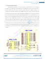
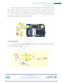
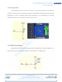
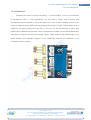
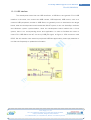
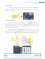
FriendlyARM English User Manual
Rev.01 (20090909)
1.3 Interface Resources Notes
This section details the development of each board or module interface definition and
occupied by pin CPU resources, CD-ROM also complete the development board schematic
and package library (divided in PDF format and Protel99SE format), for use and reference to
development board.
1.3.1 Address Space Allocation and the Definition of Chip Select Signals
S3C2440 supports two startup modes: one is startup from NAND flash (such as this
mini2440) two is startup from NOR flash. In the two startup mode, all chip select memory space
allocation is different, the following chart.
The figure above, the left is a piece nGCS0 election NOR flash memory boot mode
distribution map. The right is the NAND flash memory boot mode distribution map. Description:
Venus Supply Co., Ltd.
196/1, Soi Thedsaban-Nimit-Nau 8, Thedsaban-Nimit-Nau Road,
Ladyao, Chatuchak, Bangkok, 10900, Thailand
Tel. +(66)2954-2408 , Fax. +(66)2953-8443, Website: www.thaieasyelec.com
6
FriendlyARM English User Manual
Rev.01 (20090909)
SFR Area as a special control register address the following are the device address space
allocation and the definition of the chip select before carrying out the device address, there is
one thing to note, nGCS0 chip select space in different start-up mode, the mapping of the
device is not the same. By the map can know: in the NAND flash startup mode, the 4 Kbytes
Boot Internal SRAM be mapped to the selected nGCS0 space. In the NOR flash startup mode
(non-NAND flash boot mode), and the external memory connected nGCS0 NOR flash has been
mapped to the chip select space nGCS0 SDRAM address space: 0x30000000 - 0x34000000.
1.3.2 SDRAM Storage Systems
Mini2440 the use of two external 32 Mbytes a total of 64 Mbytes of SDRAM chip (model
as follows: HY57V561620FTP), generally referred to as memory, and then together they form a
32-bit data bus width, it can be in order to increase the speed of access, so they are used as a
chip select nGCS6, according to 5-2 in the CPU Manual Introduction, we can see that this
determines the start of their physical address is 0x30000000, the following is taken from the
schematic diagram in Mini2440 schematic diagram of the SDRAM part.
Venus Supply Co., Ltd.
196/1, Soi Thedsaban-Nimit-Nau 8, Thedsaban-Nimit-Nau Road,
Ladyao, Chatuchak, Bangkok, 10900, Thailand
Tel. +(66)2954-2408 , Fax. +(66)2953-8443, Website: www.thaieasyelec.com
7
FriendlyARM English User Manual
Rev.01 (20090909)
1.3.3 Flash Storage Systems
Mini2440 have two flashes, one is the NOR flash, model SST39VF1601, size 2 Mbytes.
The other is the NAND flash, model K9F1208, size 64 Mbytes. S3C2440 support both flash to
start the department of EC, by DIP switch S2, you can choose from NAND or NOR for your
system. Most of the actual products using a NAND flash chip are enough, because we learn for
the convenience of users, it also retains the NOR flash. NAND flash does not have the address
line, it has a dedicated control interface connected with the CPU, for the 8-bit data bus, but this
does not mean that NAND flash read and write data will be very slow. Most of the USB or SD
cards are made of NAND flash equipment. From the following schematic can be seen, NOR
flash used a total of A1-A22 address bus 22 and 16 data connected with the CPU bus, please
note the address is started from the A1, which means that each time it is the smallest unit of
read and write 2-byte. Therefore, according to schematic, the design is compatible with support
for total maximum 8 Mbytes NOR flash, the actual development of our on-board only be the A1A20 address line, as with the A21, A22 connected to the corresponding pin is SST39V1601
vacated.
Venus Supply Co., Ltd.
196/1, Soi Thedsaban-Nimit-Nau 8, Thedsaban-Nimit-Nau Road,
Ladyao, Chatuchak, Bangkok, 10900, Thailand
Tel. +(66)2954-2408 , Fax. +(66)2953-8443, Website: www.thaieasyelec.com
8
FriendlyARM English User Manual
Rev.01 (20090909)
1.3.4 Power Supply System and Interface
The development board's power supply system is relatively simple, direct the use of an
external 5 V power supply, and generated through the step-down the entire chip line unification
of the 3 required voltages: 3.3 V, 1.8 V, and 1.25 V. Please note that this development board is
not designed for handheld mobile devices, so it does not have the best power management
circuit. The whole system of power-off is controlled by the S1 DIP-switch, and it cannot switch
by machine software.
Venus Supply Co., Ltd.
196/1, Soi Thedsaban-Nimit-Nau 8, Thedsaban-Nimit-Nau Road,
Ladyao, Chatuchak, Bangkok, 10900, Thailand
Tel. +(66)2954-2408 , Fax. +(66)2953-8443, Website: www.thaieasyelec.com
9
FriendlyARM English User Manual
Rev.01 (20090909)
For the convenience of users of other external power supply, we also designed a power
supply interface CON8, it is a white 2.0 mm pitch socket single-row, middle ground both sides
are 5 V. Note that these two are not connected 5 V, one connected to the external power supply
5 V, and one connected to the DIP-switch S1 through after 5 V. Their connections and the
corresponding nominal kind of see the figure below.
1.3.5 System Reset
The development board using professional MAX811 reset chip needed to archive low
CPU reset, see the figure below.
Venus Supply Co., Ltd.
196/1, Soi Thedsaban-Nimit-Nau 8, Thedsaban-Nimit-Nau Road,
Ladyao, Chatuchak, Bangkok, 10900, Thailand
Tel. +(66)2954-2408 , Fax. +(66)2953-8443, Website: www.thaieasyelec.com
10
FriendlyARM English User Manual
Rev.01 (20090909)
1.3.6 User LED
LED is the development of the state of the most commonly used instructions of
equipment, the development board has 4 user-programmable LED, they are straight then with
the CPU of the GPIO connected, active-low (light), the detailed occupation of the resources in
the following table.
GPIO
Reusable for
Network Name
LED1
GPB5
nXBACK
nLED_1
LED2
GPB6
nXREQ
nLED_2
LED3
GPB7
nXDACK1
nLED_3
LED4
GPB8
nDREQ1
nLED_4
1.3.7 User Button
The development board has a total of 6 user button testing, they were directly from the
CPU interrupt pin to bring out a low-power level-triggered, these pins can be multiplexed and
special features for the GPIO port, in order to lead them as a user other purposes, this 6-pin
lead through CON12, and CON12 button 6 is defined as follows.
K1
K2
K3
K4
K5
K6
Corresponding interrupt
EINT8 EINT11 EINT13
EINT14 EINT15 EINT19
GPIO Reuse
GPG0
GPG3
GPG5
GPG6
GPG7 GPG11
Special function 1
nothing
nSS1 SPIMISO1 SPIMOSI1 SPICLK1 TCLK1
CON12 corresponding pin CON12.1 CON12.2 CON12.3 CON12.4 CON12.5 CON12.6
Description: CON12.7 for the power supply (3.3V), CON12.8 as to (GND)
Venus Supply Co., Ltd.
196/1, Soi Thedsaban-Nimit-Nau 8, Thedsaban-Nimit-Nau Road,
Ladyao, Chatuchak, Bangkok, 10900, Thailand
Tel. +(66)2954-2408 , Fax. +(66)2953-8443, Website: www.thaieasyelec.com
11
FriendlyARM English User Manual
Rev.01 (20090909)
1.3.8 A/D Input Test
The development board can lead to a total of 4 A/D (analog-to-digital conversion) the
conversion channel, which is located on the board of CON4 GPIO interface (see GPIO interface
introduced), in order to facilitate testing, AIN0 connected to the development of on-board
adjustable resistor W1, the principle of map are shown below.
1.3.9 PWM Control Buzzer
SPEAKER development board through the buzzer PWM control schematic diagram is as
follows, which may be conveniently GPB0 have the software set to PWM output.
Venus Supply Co., Ltd.
196/1, Soi Thedsaban-Nimit-Nau 8, Thedsaban-Nimit-Nau Road,
Ladyao, Chatuchak, Bangkok, 10900, Thailand
Tel. +(66)2954-2408 , Fax. +(66)2953-8443, Website: www.thaieasyelec.com
12
FriendlyARM English User Manual
Rev.01 (20090909)
1.3.10 Serial Port
S3C2440 own total of 3 serial ports UART0, 1, 2, which UART0, 1 may be a combination
of full-featured serial, in most applications, we only used 3 simple serial functions (this
development board provided by Linux and WinCE this driver is also installed), known as the
transmit (TxD) and receive (RxD), corresponding to their board of CON1, CON2, CON3, these 3
interfaces are drawn directly from the CPU is TTL level. For the convenience of users, their
UART0 done in RS232 level converter, which corresponds to COM0, can be directly attached to
each other to connect with PC-pass hearing. CON1, CON2, CON3 in the development of onboard location and schematic diagram of the relationship between the definitions of the
connection as shown below.
Venus Supply Co., Ltd.
196/1, Soi Thedsaban-Nimit-Nau 8, Thedsaban-Nimit-Nau Road,
Ladyao, Chatuchak, Bangkok, 10900, Thailand
Tel. +(66)2954-2408 , Fax. +(66)2953-8443, Website: www.thaieasyelec.com
13
FriendlyARM English User Manual
Rev.01 (20090909)
1.3.11 USB Interface
The development board has two USB interfaces, a USB Host, and general PC it's USB
interface is the same, can connect the USB camera, USB keyboard, USB mouse, such as a
common USB peripherals, another is USB Slave, we generally use it to download to the target
board, when the development board loaded with WinCE system, it can use ActiveSync software
and Windows system synchronization, when the development board loaded with a Linux
system, there is no corresponding driver and application. In order to facilitate the users to
control PC's USB Slave and off, we set up USB_EN signal, as figure, it CPU resources used
GPC5. We will mention more extensive peripheral USB Host application, please pay attention to
our Web site frequently to update the information.
Venus Supply Co., Ltd.
196/1, Soi Thedsaban-Nimit-Nau 8, Thedsaban-Nimit-Nau Road,
Ladyao, Chatuchak, Bangkok, 10900, Thailand
Tel. +(66)2954-2408 , Fax. +(66)2953-8443, Website: www.thaieasyelec.com
14
FriendlyARM English User Manual
Rev.01 (20090909)
1.3.12 LCD Interface
The development board of the LCD interface is a white 41-pin 0.5 mm pitch block, which
contains common LCD used most of the control signals (line-field scanning, the clock and
enable, etc.), and complete RGB data signals (RGB output 8:8:8, that can support a maximum
of 16 million colors LCD). In order to test user-friendly, but also leads to the PWM output (GPB1
can be sent configuration to keep PWM), and reset signals (nRESET), which is a backlight
control signal LCD_PWR. In addition, 37, 38, 39, 40 for the 4-wire touchscreen interface, they
can be directly connected to the use of touchscreen. J2 map board for the LCD drive power
supply selection signals, we use the board drive 5 V power supply.
Venus Supply Co., Ltd.
196/1, Soi Thedsaban-Nimit-Nau 8, Thedsaban-Nimit-Nau Road,
Ladyao, Chatuchak, Bangkok, 10900, Thailand
Tel. +(66)2954-2408 , Fax. +(66)2953-8443, Website: www.thaieasyelec.com
15
FriendlyARM English User Manual
Rev.01 (20090909)
1.3.13 EEPROM
The development board has a direct connection to CPU's I2C signal pin EEPROM chip
AT24C08, its capacity there is 256-byte, this is mainly for users to test the I2C bus, and it does
not store-specific parameters.
1.3.14 Network Interface
The development board used DM9000 LAN chip, it can be adaptive 10/100M network,
RJ45 connector internal have been included in the coupling coil, there is no need to access
another network transformers, the use of common lines of the development board can be
connected to your routers or switches.
Note: Each development board MAC address of the network is the same, it can be set
by software for Linux Users, and the relevant sections 2.4 of the manual introduce. For WinCE
users, you can refer to the DM9000 driver inside the BSP code and registry file (platform.reg).
Venus Supply Co., Ltd.
196/1, Soi Thedsaban-Nimit-Nau 8, Thedsaban-Nimit-Nau Road,
Ladyao, Chatuchak, Bangkok, 10900, Thailand
Tel. +(66)2954-2408 , Fax. +(66)2953-8443, Website: www.thaieasyelec.com
16
FriendlyARM English User Manual
Rev.01 (20090909)
1.3.15 Audio Interface
S3C2440 built-in I2S bus interface, direct external 8/16-bit stereo CODEC, the
development board used based on the I2S bus UDA1341 system audio decoder chip, the
internal chip's registers are initialized and set up mining L3-bus with the bus connection control
achieved, where we have used for a public board of Samsung design, respectively, the use of
CPU's GPB2, GPB3, GPB4 port simulation of the L3-Bus specification L3MODE, L3DATA,
L3CLOCK, their initialization end after UDA1341 are no longer useful, so these 3 control lines
can also be used to achieve a common single-chip simulation. The output of audio systems for
the development of common on-board aperture 3.5 mm socket, type is divided into 2 roads, all
the way for the board Michael Grams of the wind, and the other way through the 2.0 mm socket
CON10 white lead. 2-way audio input of the driver is different, only CON10 corresponding
channel interface can be used in sound recording, please refer to our website update
information, the 2 channels we will drive up the end.
1.3.16 JTAG Interface
When the development board from the patch works offline, there is no process, then we
generally through the JTAG interface programmer the first procedure is Supervivi, with Supervivi
I can use USB to download more complex system procedures, this section at the back you can
see. In addition, JTAG interface in the development of the most common is the single-step
debugging purposes, whether it is common market JLINK or ULINK, as well as other simulation
Venus Supply Co., Ltd.
196/1, Soi Thedsaban-Nimit-Nau 8, Thedsaban-Nimit-Nau Road,
Ladyao, Chatuchak, Bangkok, 10900, Thailand
Tel. +(66)2954-2408 , Fax. +(66)2953-8443, Website: www.thaieasyelec.com
17
FriendlyARM English User Manual
Rev.01 (20090909)
debugger, and ultimately are connected through the JTAG interface. Standard JTAG interface is
a 4-wire: TMS, TCK, TDI, TDO, respectively, for mode selection, clock, data input and data
output lines, together with the power and that a total of six lines in general is enough, for the
convenience of debugging, the majority of simulator also provides a reset signal. Therefore, the
standard JTAG interface is mentioned above refers to whether the JTAG signal lines are not 20pin or 10-pin formal definition of such performance. This is like USB interface, can be a side can
be flat, also can be other forms of, as long as these interfaces includes a complete line of JTAG
signals can be referred to as the standard JTAG interface. The development board provides a
JTAG standard signal that contains the complete 10-pin JTAG interface, the definition of the pin
shown in figure. Description: The intention is committed to Linux or WinCE for beginners in terms
of development, JTAG interface is not essential any meaning and purpose, as most boards
have been developed to provide a complete BSP, which includes the most common serial and
network USB communications network, as well as I, when the system can be loaded with Linux
or WinCE operating system, the user can fully use variety of high-level debugging operating
system features, then do not need JTAG interface. Even if you need for tracking, but in view of
the operating system, the complex structure of many interfaces, single-step debug like a needle
in a haystack, there is no significance to speak of. Think about your use of the PC-on-hand will
know, perhaps you have never seen or even heard of who in the PC motherboard play an
emulator to debug PCI interface so Windows XP or Linux driver. This is why you, as common to
hear or talk about so many people drive in the "transplant", because most people do refer to the
achievement of senior-driven. JTAG is only for the user who not intends to install the operating
system or to use simple operating system (for example uCos2, etc.). Development board
provided by the majority of the Bootloader or BIOS is a basic system intact, and therefore do not
need to single-step debugging.
Venus Supply Co., Ltd.
196/1, Soi Thedsaban-Nimit-Nau 8, Thedsaban-Nimit-Nau Road,
Ladyao, Chatuchak, Bangkok, 10900, Thailand
Tel. +(66)2954-2408 , Fax. +(66)2953-8443, Website: www.thaieasyelec.com
18
FriendlyARM English User Manual
Rev.01 (20090909)
1.3.17 GPIO
GPIO is common referred to as input-output port. The development board with a 34-pin
2.0 mm pitch GPIO interface nominal for CON4, figure. In fact, CON4 surplus not only includes a
lot of the GPIO pins, also contains a number of other CPU-pin, if AD0-AIN3, CLKOUT, etc. The
map you see in the SPI interface, I2C interface, GPB0 and GPB1 and so on, it who is also GPIO,
but special features are the definition of the nominal interface, these are available through the
corresponding CPU storage to set their browser to change the use of the resources detailed in
the table below the interface.
CON4
1
Network
Name
VDD5V
3
5
7
9
11
13
15
GND
AIN0
AIN2
EINT0
EINT2
EINT4
EINT6
Help
(some ports reusable)
5V power supply
(input or output)
ground
AD input channel 0
AD input channel 2
EINT0/GPF0
EINT2/GPF2
EINT4/GPF4
EINT6/GPF6
CON4
2
Network
Name
VDD33V
4
6
8
10
12
14
16
nRESET
AIN1
AIN3
EINT1
EINT3
EINT5
EINT8
Help
(some ports reusable)
3.3V power supply
(output)
Reset signal (output)
AD input channel 1
AD input channel 3
EINT1/GPF1
EINT3/GPF3
EINT5/GPF5
EINT8/GPG0
Venus Supply Co., Ltd.
196/1, Soi Thedsaban-Nimit-Nau 8, Thedsaban-Nimit-Nau Road,
Ladyao, Chatuchak, Bangkok, 10900, Thailand
Tel. +(66)2954-2408 , Fax. +(66)2953-8443, Website: www.thaieasyelec.com
19
FriendlyARM English User Manual
Rev.01 (20090909)
CON4
17
19
21
23
25
27
29
31
33
Network
Help
CON4 Network
Help
Name
(some ports reusable)
Name
(some ports reusable)
EINT9
EINT9/GPG1
18
EINT11
EINT11/GPG3/nSS1
EINT13 EINT13/GPG5/SPIMISO1 20
EINT14 EINT14/GPG6/SPIMOSI1
EINT15 EINT15/GPG7SPICLK1 22
EINT17
EINT17/GPG9/nRST1
EINT18
EINT18/GPG10/nCTS1
24
EINT19
EINT19/GPG11
SPIMISO
SPIMISO/GPE11
26
SPIMOSI SPIMOSI/EINT14/GPG6
SPICLK
SPICLK/GPE13
28
nSS_SPI nSS_SPI/EINT10/GPG2
I2CSCL
I2CSCL/GPE14
30
I2CSDA
I2CSDA/GPE15
GPB0
TOUT0/GPB0
32
GPB1
TOUT1/GPB1
CLKOUT0
CLKOUT0/GPH9
34 CLKOUT1
CLKOUT1/GPH10
1.3.18 CMOS CAMERA Interface
S3C2440 with a CMOS camera interface, in the development of on-board through the
nominal interface leads to CAMERA. It is a 20-pin 2.0 mm pitch pin blocks, users can provide us
with direct access to the CAM130 camera module. Fact CAM130 camera module without any
circuit above, it is only a relay board, it is directly connected to the use of model ZT130G2
camera module, which is defined as shown in Fig. Description: CAMERA multiplexing interface
is a port, it can be changed to set the corresponding GPIO enable register Use the following
table is a list of the corresponding GPIO pin.
Venus Supply Co., Ltd.
196/1, Soi Thedsaban-Nimit-Nau 8, Thedsaban-Nimit-Nau Road,
Ladyao, Chatuchak, Bangkok, 10900, Thailand
Tel. +(66)2954-2408 , Fax. +(66)2953-8443, Website: www.thaieasyelec.com
20
FriendlyARM English User Manual
Rev.01 (20090909)
CAMERA
1
3
5
7
9
11
13
15
17
19
Network
Reusable
name
I2CSDA
GPE15
EINT20
GPG12
CAMCLK
GPJ11
CAM_VSYNC
GPJ9
CAMDATA7
GPJ7
CAMDATA5
GPJ5
CAMDATA3
GPJ3
CAMDATA1
GPJ1
VDD33V
3.3V power supply
VDD18V
1.8V power supply
CAMERA
2
4
6
8
10
12
14
16
18
20
Network
name
I2CSCL
CAMRST
CAM_HREF
CAM_PCLK
CAMDATA6
CAMDATA4
CAMDATA2
CAMDATA0
VDD_CAM
GND
Reusable
GPE14
GPJ12
GPJ10
GPJ8
GPJ6
GPJ4
GPJ2
GPJ0
VDD_CAM
ground
1.3.19 System Bus Interface
The development board for the system bus interface CON5, it contains a total of 16 data
lines (D0-D15), 8 address lines (A0-A6, A24), there are some control signal lines (chip select,
read and write, reset, etc.), CON5 can provide 5V voltage lose out A; a matter of fact, very few
users to expand the peripheral bus. The following is the definition of CON5 detailed description
pin.
Venus Supply Co., Ltd.
196/1, Soi Thedsaban-Nimit-Nau 8, Thedsaban-Nimit-Nau Road,
Ladyao, Chatuchak, Bangkok, 10900, Thailand
Tel. +(66)2954-2408 , Fax. +(66)2953-8443, Website: www.thaieasyelec.com
21
FriendlyARM English User Manual
Rev.01 (20090909)
1
Network
Name
VDD5V
3
5
7
EINT17
EINT3
nGCS1
9
nGCS3
11
13
15
17
19
21
23
25
27
29
31
33
35
37
39
LnOE
nWAIT
nXDACK0
LADDR0
LADDR2
LADDR4
LADDR6
LDATA0
LDATA2
LDATA4
LDATA6
LDATA8
LDATA10
LDATA12
LDATA14
CON5
Help
CON5
(some ports reusable)
5V power supply
2
(input or output)
Interruption 17 (input)
4
Interruption 3 (input)
6
Chip Select 1
8
The corresponding
physical address:
0x08000000
Chip Select 3
10
The corresponding
physical address:
0x18000000
Read enable signal
12
Wait for signal
14
nXDACK0
16
Address 0
18
Address 2
20
Address 4
22
Address 6
24
Data line 0
26
Data line 2
28
Data line 4
30
Data line 6
32
Data line 8
34
Data line 10
36
Data line 12
38
Data line 14
40
Network
Name
GND
Help
(some ports reusable)
ground
EINT18
EINT9
nGCS2
Interruption 18 (input)
Interruption 9 (input)
Chip Select 2
The corresponding
physical address:
0x10000000
Chip Select 5
The corresponding
physical address:
0x28000000
Write enable Signal
Reset
nXDREQ0
Address 1
Address 3
Address 5
Address 7
Data line 1
Data line 3
Data line 5
Data line 7
Data line 9
Data line 11
Data line 13
Data line 15
nGCS5
LnWE
nRESET
nXDREQ0
LADDR1
LADDR3
LADDR5
LADDR7
LDATA1
LDATA3
LDATA5
LDATA7
LDATA9
LDATA11
LDATA13
LDATA15
Venus Supply Co., Ltd.
196/1, Soi Thedsaban-Nimit-Nau 8, Thedsaban-Nimit-Nau Road,
Ladyao, Chatuchak, Bangkok, 10900, Thailand
Tel. +(66)2954-2408 , Fax. +(66)2953-8443, Website: www.thaieasyelec.com
22