1
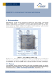
APPLICATION NOTE 502 Dolphin In-Circuit programming – Updating Firmware in the field 1 Introduction In systems e.g. gateways, where an external microcontroller is connected to a Dolphin based product like a TCM300 it might be desirable to be able to program the Dolphin Flash memory. This for instance can be used to apply program updates providing the new FLASH image via a backbone to the host micro controller. The host micro controller can than reprogram the Dolphin (target) FLASH memory. EnOcean Gateway Dolphin uC Target Backbone Host uC Figure 1 – System overview This application note describes the programming hardware interface and the communication protocol between the host and target microcontroller. Additionally it describes how to implement the programming functionality on a host using a Freescale 32bit ColdFire microcontroller (MCF52233 Demo Board) attached to a TCM300 evaluation board (EVA300) as shown in Figure 2. Host uC Dolphin uC Target Figure 2 - Dolphin programming setup using ColdFire microcontroller © EnOcean | www.enocean.com Subject to modifications | Product Marketing | June 2011 | Page 1/ 21 APPLICATION NOTE 502 DOLPHIN IN-CIRCUIT PROGRAMMING – UPDATING FIRMWARE IN THE FIELD This documentation and software project can be the basis for own developments and can also be used to develop programming adapters. For easier readability and portability the host software was implemented without the use of an operating system. The focus was put on demonstrating the basic functionality rather than demonstrating a real e.g. gateway application. 1.1 References Further details can be found in the following documentation [1.] DolphinAPI user manual, EO3000I_API.chm, 1.1.0.0 [2.] DolphinStudio manual (containing EOPX documentation), DolphinStudio.chm [3.] Schematics EVA300-3 [4.] ColdFire M52233 demo Evaluation board schematics [5.] Intel hex file format (http://de.wikipedia.org/wiki/Intel_HEX) Useful web sites: [6.] EnOcean website http://www.enocean.com [7.] Wikipedia website http://www.wikipedia.org/ [8.] Freescale website http://www.freescale.com 1.2 System overview Figure 3 shows the interactions of the various components and files used in the develop- ment flow of the Dolphin module on one side and the flow on the host microcontroller on the other. Due to the implementation on the Dolphin (also see Hex to C-source file converter (EOMC.exe)) there are two hex files generated by the EOPX (eopx.exe) post build tool. There is the hex file containing the data which is located in the program area and there is a second hex file containing the data which is located in the configuration area of the Dolphin’s Flash memory. The EOPX post build tool performs all the required modifications and extraction necessary to generate those two hex files based on the hex file generated by the linker. E.g. is the program size (u8PrgSize) calculated and entered into the configuration area hex file and the CRC for the BIST (built-in self test) is calculated and entered in to the program area hex file. Both hex files together contain the complete data to program the Dolphin Flash memory. In this application note those two files are converted (see next chapter) into c language source files which are then statically compiled and linked into the host microcontroller application. Like this it is easy to demonstrate the principle of the programming without adding further complexity of handling of the files e.g. over a TCP/IP backbone. This handling will strongly depend on the application requirements and therefore will be system specific. © EnOcean | www.enocean.com Subject Subjecttotomodifications modifications| Wolfgang | Product Marketing Bihlmayr | June 2011 | Page 2/ 21 APPLICATION NOTE 502 DOLPHIN IN-CIRCUIT PROGRAMMING – UPDATING FIRMWARE IN THE FIELD Prg Area (hex file) DolphinStudio API Config.files User Source Code EOMC Converter Controlled from Keil IDE Keil Compiler API Library Cfg Area (hex file) Keil Linker ProgData (c file) User Source Code Compiler/Linker Host (e.g. CodeWarrior) EOPX PostBuild PostBuild.txt Host Application Prg Area (hex file) Cfg Area (hex file) Target Dolphin uC Host uC Software Development Flow Target Software Development Flow Host Figure 3 – System interactions 1.3 Hex to C-source file converter (EOMC.exe) The EOMC command line tool converts the two hex files generated by Keil (EOPX post build) into a c language source code file. The program area hex file is simply converted in an array of bytes u8PrgData[]. For the configuration area the process is a little more complex. The input file format used is Intel HEX (also see [5.] Intel hex file format (http://de.wikipedia.org/wiki/Intel_HEX)). The hex file consists of records which contain amongst others the address and the data located at this address. Like this it is possible to code single bytes in a block of memory without defining the values of the bytes in-between. For the configuration area this method is used to only program (modify) specific bytes (e.g. u8PrgSize) without modifying others (e.g. calibration values). That’s why the EOMC generates two arrays for the configuration area an u8CfgData[256] and an u8CfgMask[256] array. The data lists the bytes to program and the mask defines if a byte needs to be programmed (=0xFF) or not (=0x00). for(i=0;i<256;i++) if(u8CfgMask[i]!=0) tCfgArea.raw.bytes[i] = u8CfgData[i]; © EnOcean | www.enocean.com // modify CFG area Subject Subjecttotomodifications modifications| Wolfgang | Product Marketing Bihlmayr | June 2011 | Page 3/ 21 APPLICATION NOTE 502 DOLPHIN IN-CIRCUIT PROGRAMMING – UPDATING FIRMWARE IN THE FIELD EOMC usage: Eomc.exe –fprg <prgarea.hex> -fcfg <cfgarea.hex> -fout prgfile 1.4 FLASH memory organization The Dolphin FLASH is organized in pages of 256 bytes size. A total of 129 pages (32kByte + 256byte) of FLASH are available. The total FLASH memory is split into 3 areas as indicated in Figure 4: Program and Data Area Information Area (chip specific data) Configuration Area (module specific data) 0x0000 0x0100 page 0 0x00FF page 1 0x01FF Program & Data Area 0x7E00 0x9F00 page 126 Configuration Area (page 127) 0xA000 0x7EFF 0x9FFF Information Area (page 128) 0xA0FF Figure 4 – FLASH areas The FLASH memory can be programmed on a byte level. Erasing its only possible on a page level, erasing the whole 256 bytes at once. The erased state of the FLASH is all bits set and an erased byte reads 0xFF. 1.4.1 Program and Data Area The FLASH from address The compiled hex file is aligns the hex file to the CRC value is used for the © EnOcean | www.enocean.com 0x0000 to 0x7EFF is used for the program and data information. placed into this memory area. The EOPX post build tool always 256 page boundary and adds as the last byte a CRC value. This flash BIST (built-in-self-test). Subject Subjecttotomodifications modifications| Wolfgang | Product Marketing Bihlmayr | June 2011 | Page 4/ 21 APPLICATION NOTE 502 DOLPHIN IN-CIRCUIT PROGRAMMING – UPDATING FIRMWARE IN THE FIELD For instance if the compiled program size is 256 byte - after the alignment with EOPX post build - it will consume 512 bytes (2 pages) in the FLASH memory (from 0x0000 - 0x01FF). The last byte of the downloaded code will be the CRC value (at address 0x01FF) used for the BIST. The last page of the program and data area (0x7E00 to 0x7eFF) is intended to be used as Log Area (see [1.] DolphinAPI user manual, EO3000I_API.chm, 1.1.0.0). 1.4.2 Information Area The information area contains chip specific data like e.g. the chip id and manufacturing trace information. The memory page 128 at address 0xA000-0xA0FF is used for this purpose. The information is collected during chip manufacturing and testing and is read-only. 1.4.3 Configuration Area The configuration area contains module specific data like calibration values. The FLASH memory page 127 at address 0x9F00-0x9FFF is used for this purpose. Figure 5 – Configuration Area (CFG_AREA) The information in this page is collected partly during module manufacturing and testing (first 128 bytes) and can also be used for customer specific information (second 128 bytes). The page is read-write and can always be read even if the code protection is set. Due to the fact that the whole page has to be erased to modify a single byte special care has to be taken to avoid loosing the module specific data. This area also contains the program size information (at address 0x9F00) which typically needs modification after a reprogramming. Note: The first 4 bytes from address 0x9F00-0x9F03 require special handling. Erasing of those bytes is only possible by executing the WR_PRG_AREA (executes mass erase) command. Programming is only possible using the WR_FLASH_BYTE command. In programming mode the CFG_AREA is mapped to other memory space as in program runtime. If you access CFG_AREA in programming mode using WR_FLASH_BYTE, RD_FLASH_BYTE use the addresses 0x7F00 – 0x7FFF. © EnOcean | www.enocean.com Subject Subjecttotomodifications modifications| Wolfgang | Product Marketing Bihlmayr | June 2011 | Page 5/ 21 APPLICATION NOTE 502 DOLPHIN IN-CIRCUIT PROGRAMMING – UPDATING FIRMWARE IN THE FIELD 1.4.4 Code Protection The program and data area can be protected against readout (e.g. to inhibit reverse engineering) with the code protection. When the code protection is set the program and data area can't be read with an external programmer. The only way to reset the code protection is done by erasing the whole program and data area with the WR_PRG_AREA (executes mass erase) command. The information area and the configuration area can be always read even if code protection is set. The code protection is the second byte in the configuration area at address 0x9F01: Code protection set (0x00) No code protection set (0x0FF) To enable the code protection the WR_FLASH_BYTE command (address 0x9F01, data 0x00) has to be used. 2 Programmer 2.1 Hardware Interface The programming interface is based around a standard 4 wire SPI (Serial Peripheral Interface) together with three additional control signals. The host acts as SPI master (controlling the SPI communication and providing the clock) and the target (Dolphin) acts as SPI slave. The 3 additional (to the 4 SPI) signals are: RESET signal to reset the target READY signal for synchronisation between host and target PMODE signal to enter programming (boot loader) mode. HOST QSPI_CS0 QSPI_SCK QSPI_DO QSPI_DI PUB[0](UTXD1) PUB[1](URXD1) PUB[2](UCTS1) GND Dolphin CS# SCSEDIO0 CLK MOSI MISO READY PMODE RESET SCLKDIO1 WSDADIO2 RSDADIO3 ADIO7(READY) PROG_EN RESET GND Figure 6 –Programmer Interface Signals © EnOcean | www.enocean.com Subject Subjecttotomodifications modifications| Wolfgang | Product Marketing Bihlmayr | June 2011 | Page 6/ 21 APPLICATION NOTE 502 DOLPHIN IN-CIRCUIT PROGRAMMING – UPDATING FIRMWARE IN THE FIELD 2.2 Programming Algorithm / Flow Figure 7 depicts the programming flow for the Dolphin module. First step is to establish the connection between the host and the target. During connect the Dolphin module is reset and started into boot loader (programming) mode. To verify the logical connection the RD_SW_VERSION command is executed. If the command receives a valid answer the connection is established. Next the information area (optional) and the configuration area are read. The configuration area is then selectively modified using the u8CfgData[] and u8CfgMask[] arrays (also see 1.3 Hex to C-source file converter (EOMC.exe)). Connect Read INF Area Read CFG Area PrgData.c u8CfgData[], u8CfgMask[] Modify CFG Area (Mass Erase) PrgData.c u8PrgData[] Write PRG Area Write CFG Area Execute BIST Verify CodeProtection? yes Set CodeProtection no Disconnect Figure 7 - Programming flow © EnOcean | www.enocean.com Subject Subjecttotomodifications modifications| Wolfgang | Product Marketing Bihlmayr | June 2011 | Page 7/ 21 APPLICATION NOTE 502 DOLPHIN IN-CIRCUIT PROGRAMMING – UPDATING FIRMWARE IN THE FIELD Then the whole Flash is erased and the program data (using the u8PrgData[] array) is written. Both steps are done with the WR_PRG_AREA command. Afterwards the modified configuration area is written using the WR_FLASH_PAGE and WR_FLASH_BYTE (for the first 2 bytes) commands. Then the proper execution of the BIST (built-in-self-test) is verified. To verify correct programming a byte-by-byte comparison of the configuration area and the program area is performed. Note: The intention of the CRC is to verify FLASH integrity over the life time (in system). The “only” 8 bit CRC should not be used to ensure that the programming was correctly executed. Finally after verifying correct programming the code protection (optional) can be set if desired. During disconnect the Dolphin module is reset into user mode and the programming signals are turned to inputs (high impedance state). Note: The error handling used in this implementation only executes a step if no error has occurred previously. Exception is the Disconnect which is always executed. For further details please see source code. 2.3 Mode selection 2.3.1 RESET signal The RESET signal allows the host to reset the Dolphin. In combination with the PMODE signal it’s possible to enter either boot loader mode (programming) or user mode (application code running). Note: The RESET signal is active high! 2.3.2 PMODE signal (PROGEN) With the falling edge of the RESET the Dolphin and starts to execute code in the ROM at address 0x0000. The first instructions poll the state of the PROGEN pin to decide if the boot loader code (ROM) is executed or the user application code (FLASH) is started. In case of the boot loader mode the READY signal is used to indicate that the target is ready to receive SPI transfers (commands). In case of the application code the state of the READY signal depends on the software (ADIO7). © EnOcean | www.enocean.com Subject Subjecttotomodifications modifications| Wolfgang | Product Marketing Bihlmayr | June 2011 | Page 8/ 21 APPLICATION NOTE 502 DOLPHIN IN-CIRCUIT PROGRAMMING – UPDATING FIRMWARE IN THE FIELD RESET PMODE READY Mode Boot loader mode User mode TProgenH Figure 8 – Mode selection 2.4 Communication protocol The boot loader communication protocol is based on 32 bit SPI transfers in combination with a synchronization mechanism using the READY signal. 2.4.1 SPI protocol The underlying SPI protocol uses a low active chip select (CS#). With each SPI transfer (CS# low pulse) 4 bytes of data (32 bits) are transferred. Each byte is transferred with the most significant bit (MSB) B7 first. The SPI clock signal is low when inactive. With the leading edge (rising edge) of the clock signal the data bits are sampled. With the following edge (falling edge) of the clock the data bits have to be applied. CS# Clock HOST (MOSI) DOLPHIN (MISO) B7 B6 B5 B4 B3 B2 B1 B0 B7 B6 B5 B4 B3 B4 B3 B2 B1 B0 B7 B6 B5 B4 B3 B2 B1 B0 B7 B6 B5 B4 B3 B4 B3 B2 B1 B0 Figure 9 – SPI Transfer The whole communication is only using half-duplex transfers meaning that data is exchanged either only from host to target or vice-versa. The listening communication node sends idle data (0x00). 2.4.2 READY signal The READY signal is used by the target to signal when it is ready to receive data. If the READY signal is low the target is busy and it’s not allowed to send data. After every SPI transfer there is a certain delay before the READY signal is set low. Depending on the commands the READY signal might be low (busy) in a range from 10us up to 60ms. © EnOcean | www.enocean.com Subject Subjecttotomodifications modifications| Wolfgang | Product Marketing Bihlmayr | June 2011 | Page 9/ 21 APPLICATION NOTE 502 DOLPHIN IN-CIRCUIT PROGRAMMING – UPDATING FIRMWARE IN THE FIELD CS# Clock Data 32 bit 32 bit READY TReadyD TBusy Figure 10 – READY signal 2.4.3 Timing Characteristics Parameter Symbol Max. SPI frequency Min. f_SPI RESET active (high) time READY delay time PROG_EN hold time Target Busy time (READY low) Max. Unit 2 MHz T_RESET 1000 us T_READYD 30 us T_PROGENH 500 us T_BUSY 10 60000 us 2.5 Command triggered protocol The communication uses a command triggered approach. Only the host triggers any communications using commands. The Dolphin executes the desired command and receives or transmits the required data and/or acknowledge. All commands are packed into 8 bytes requiring 2 (32 bit) SPI transfers. CS# Clock HOST (MOSI) 32 bit DOLPHIN (MISO) 32 bit 32 bit 32 bit Figure 11 – communication protocol (half duplex) Note: The host has to monitor the READY signal after every 32 bit SPI transfers (also in-between the two 32 bit transfers for a command). © EnOcean | www.enocean.com Subject Subjecttotomodifications modifications| Wolfgang | Product Marketing Bihlmayr | June 2011 | Page 10/ 21 APPLICATION NOTE 502 DOLPHIN IN-CIRCUIT PROGRAMMING – UPDATING FIRMWARE IN THE FIELD As already mentioned is the communication half-duplex, e.g. the host sends a command with the first data frame (Dolphin sends idle (0x00)). Than the host basically only provides the clock (host sends idle (0x00)) to request a response data frame. 2.5.1 Commands The commands are embedded in a header of three fixed byte, the actual command identifier byte, three byte of optional additional parameters and a checksum byte resulting in a total length of 8 byte. Note: n/d means bytes are not defined an can have any values The following features are provided: Read boot loader software version Read FLASH (1 byte, 1 page, program area) Write FLASH (1 byte, 1 page, program area) Erase FLASH (1 page, Mass erase) -> see Write FLASH commands Blank test (verify that erased) BIST (verify BIST setting) Write to XRAM and execute (for testing) Command Byte0 Byte1 Byte2 Byte3 Byte4 Byte5 Byte6 Byte7 (CMD) RD_SW_VERSION 0x4B 0x00 0x00 0x00 INF_SW_VERSION 0x8C SW1 SW2 SW3 RD_FLASH_BYTE 0x6B AddHi AddLo 0x00 WR_FLASH_BYTE 0x6C AddHi AddLo Data RD_FLASH_PAGE 0x69 PageIdx 0x00 0x00 WR_FLASH_PAGE 0x6A PageIdx EraseOnly 0x00 0x6D PageCnt 0x00 WR_PRG_AREA 0x6E PageCnt EraseOnly INF_OK 0x58 Code n/d n/d INF_ERROR 0x99 ECode n/d n/d WR_BLANK_CHK 0x70 0x00 0x00 0x00 WR_BIST 0x71 0x00 0x00 0x00 WR_PRG_XRAM 0x6F PageCnt 0x00 0x00 RD_PRG_AREA 0xA5 0x5A 0xA5 0x00 checksum 0x00 Table 1 – Command list © EnOcean | www.enocean.com Subject Subjecttotomodifications modifications| Wolfgang | Product Marketing Bihlmayr | June 2011 | Page 11/ 21 APPLICATION NOTE 502 DOLPHIN IN-CIRCUIT PROGRAMMING – UPDATING FIRMWARE IN THE FIELD 2.5.2 Checksum The checksum is the sum (modulo 256) over the Byte2 to Byte6, e.g. uint8 u8checksum; for (i=2; i<7; i++) u8checksum += u8Byte[i]; 2.5.3 RD_SW_VERSION The RD_SW_VERSION command is used to retrieve the boot loader software version. The target responds with the INF_SW_VERSION. This command is used after entering boot loader mode to ensure proper mode selection. Command RD_SW_VERSION HOST (MOSI) Byte0 Byte1 Byte2 CMD Byte4 Byte5 Byte6 Byte7 0xA5 0x5A 0xA5 0x4B 0x00 0x00 0x00 checksum RD_SW_VERSION DOLPHIN INF_SW_VERSION (MISO) Figure 12 – Command RD_SW_VERSION 2.5.4 INF_SW_VERSION The INF_SW_VERSION sends the boot loader software version to the host. Command INF_SW_VERSION Byte0 Byte1 Byte2 CMD Byte4 Byte5 Byte6 Byte7 0xA5 0x5A 0xA5 0x8C SW1 SW2 SW3 checksum Parameters: SW1 SW2 SW3 2.5.5 Main version number Beta version number Alpha version number RD_FLASH_BYTE The RD_FLASH_BYTE command reads one byte of FLASH specified by the AddHi, AddLo parameters. The target acknowledges with an INF_OK containing the requested data in the Code field. Command RD_FLASH_BYTE © EnOcean | www.enocean.com Byte0 Byte1 Byte2 CMD Byte4 Byte5 Byte6 Byte7 0xA5 0x5A 0xA5 0x6B AddHi AddLo 0x00 checksum Subject Subjecttotomodifications modifications| Wolfgang | Product Marketing Bihlmayr | June 2011 | Page 12/ 21 APPLICATION NOTE 502 DOLPHIN IN-CIRCUIT PROGRAMMING – UPDATING FIRMWARE IN THE FIELD HOST (MOSI) RD_FLASH_BYTE DOLPHIN INF_OK (Data) (MISO) Figure 13 – Command RD_FLASH_BYTE Parameters: AddHi AddLo High-Byte of the address to read Low-Byte of the address to read Note: In programming mode the CFG_AREA is mapped to other memory space as in program runtime. Use the addresses 0x7F00 – 0x7FFF. If the address is in the program area and the code protect is set then an INF_ERROR (ECode ERR_READONLY) is replied. If the address is out of the ERR_OUT_OF_MEMORY) is replied. 2.5.6 FLASH memory than an INF_ERROR (ECode WR_FLASH_BYTE The WR_FLASH_BYTE command writes the data byte to the specified memory address. The target sends an INF_OK response. Command WR_FLASH_BYTE HOST (MOSI) Byte0 Byte1 Byte2 CMD Byte4 Byte5 Byte6 Byte7 0xA5 0x5A 0xA5 0x6C AddHi AddLo Data checksum WR_FLASH_BYTE DOLPHIN (MISO) INF_OK Figure 14 – Command WR_FLASH_BYTE Parameters: AddHi High-Byte of the address to read AddLo Low-Byte of the address to read Data Data byte to write Note: In programming mode the CFG_AREA is mapped to other memory space as in program runtime. Use the addresses 0x7F00 – 0x7FFF. If the address is in the information area an INF_ERROR (ECode ERR_READONLY) is rep- lied. © EnOcean | www.enocean.com Subject Subjecttotomodifications modifications| Wolfgang | Product Marketing Bihlmayr | June 2011 | Page 13/ 21 APPLICATION NOTE 502 DOLPHIN IN-CIRCUIT PROGRAMMING – UPDATING FIRMWARE IN THE FIELD If the address is in the program area and the code protection is set an INF_ERROR (ECode ERR_CODEPROTECTION) is replied. If the address is not erased (0xFF) then INF_ERROR (ECode ERR_BYTE_NOT_ERASED) is replied. If the address is out of the ERR_OUT_OF_MEMORY) is replied. 2.5.7 FLASH memory than an INF_ERROR (ECode RD_FLASH_PAGE The RD_FLASH_PAGE command reads a page (256 byte) specified by the PageIdx of FLASH memory. The target first sends an acknowledge INF_OK before it send the 256 bytes of FLASH content. Command RD_FLASH_PAGE HOST (MOSI) Byte0 Byte1 Byte2 CMD Byte4 Byte5 Byte6 Byte7 0xA5 0x5A 0xA5 0x69 PageIdx 0x00 0x00 checksum RD_FLASH_PAGE DOLPHIN INF_OK (MISO) FLASH_PAGE(256 Byte) Figure 15 – Command RD_FLASH_PAGE Parameters: PageIdx Index of the page to read (0..128) Note: If the page is in the program area and the code protection is set then an INF_ERROR (ECode ERR_READONLY) is replied. If the PageIdx is out of the range an INF_ERROR (ECode ERR_OUT_OF_MEMORY) is rep- lied. 2.5.8 WR_FLASH_PAGE The WR_FLASH_PAGE command writes one page (256 byte) to the specified page of FLASH memory. It handles the following steps: erasing of the page blank check of the page writing of the 256 bytes of data First the target responds with an acknowledge INF_OK. Then the host sends the 256 bytes of data. The target response with an INF_OK. Command WR_FLASH_PAGE © EnOcean | www.enocean.com Byte0 Byte1 Byte2 0xA5 0x5A 0xA5 CMD 0x6A Byte4 Byte5 PageIdx EraseOnly Byte6 Byte7 0x00 checksum Subject Subjecttotomodifications modifications| Wolfgang | Product Marketing Bihlmayr | June 2011 | Page 14/ 21 APPLICATION NOTE 502 DOLPHIN IN-CIRCUIT PROGRAMMING – UPDATING FIRMWARE IN THE FIELD HOST (MOSI) WR_FLASH_PAGE FLASH_PAGE(256 Byte) DOLPHIN INF_OK (MISO) INF_OK Figure 16 – Command WR_FLASH_PAGE Additionally it’s possible to only erase the page without writing of data. This is done by setting the EraseOnly parameter to 0x01. In this case also no data is transferred. HOST (MOSI) WR_FLASH_PAGE DOLPHIN INF_OK (MISO) Figure 17 – Command WR_FLASH_PAGE (Erase Only) Parameters: PageIdx Index of the page to write/erase (0..127) 0x00 erase and write page EraseOnly 0x01 erase page Note: the first four bytes in the configuration area can not be programmed or erased with this command (remain unchanged) If the code protection is set then an INF_ERROR (ECode ERR_READONLY) is replied. If the PageIdx 128 (information area) is used an INF_ERROR (ECode ERR_READONLY) is replied. If the PageIdx is >128 an INF_ERROR (ECode ERR_OUT_OF_MEMORY) is replied. In case of an error during FLASH program operation an ERR_WRITING_FAILED or ERR_ERASE_FAILED) is replied. 2.5.9 INF_ERROR (ECode RD_PRG_AREA Reads the program area starting from address 0x0000 up to the specified number of pages. The target first sends an acknowledge INF_OK before it sends the PageCnt * 256 byte of FLASH content. Command Byte0 RD_PRG_AREA HOST (MOSI) 0xA5 Byte1 Byte2 0x5A 0xA5 CMD Byte4 Byte5 Byte6 Byte7 0x6D PageCnt 0x00 0x00 checksum RD_PRG_AREA DOLPHIN (MISO) INF_OK PRG_AREA (PageCnt * 256 byte) Figure 18 – RD_PRG_AREA © EnOcean | www.enocean.com Subject Subjecttotomodifications modifications| Wolfgang | Product Marketing Bihlmayr | June 2011 | Page 15/ 21 APPLICATION NOTE 502 DOLPHIN IN-CIRCUIT PROGRAMMING – UPDATING FIRMWARE IN THE FIELD Parameters: PageCnt Number of pages to read (1..127) Note: If the code protect is set then an INF_ERROR (ECode ERR_CODEPROTECTION) is replied. If the PageCnt is >127 an INF_ERROR (ECode ERR_OUT_OF_MEMORY) is replied. 2.5.10 WR_PRG_AREA The WR_PRG_AREA command writes PageCnt * 256 byte of data to the program area starting at address 0x0000. It handles the following steps: mass erasing of the program area erase of the configuration area blank check of program and configuration area writing of the of data First the target responds with an acknowledge INF_OK. Then the host sends the PageCnt * 256 byte of data. The target responds with an INF_OK. Command Byte0 WR_PRG_AREA HOST (MOSI) 0xA5 Byte1 Byte2 0x5A 0xA5 WR_PRG_AREA DOLPHIN CMD 0x6E Byte4 Byte5 PageCnt EraseOnly Byte7 0x00 checksum PRG_AREA (PageCnt * 256 byte) INF_OK (MISO) Byte6 INF_OK Figure 19 – Command WR_PRG_AREA Additionally it’s possible to only erase without writing of data. This is done by setting the EraseOnly byte to 0x01. In this case also no data is transferred. HOST (MOSI) WR_PRG_AREA DOLPHIN (MISO) INF_OK Figure 20 – Command WR_PRG_AREA (Erase Only) Parameters: PageCnt EraseOnly Number of the pages to write/erase (1..127) 0x00 mass erase and write of pages 0x01 mass erase Note: © EnOcean | www.enocean.com Subject Subjecttotomodifications modifications| Wolfgang | Product Marketing Bihlmayr | June 2011 | Page 16/ 21 APPLICATION NOTE 502 DOLPHIN IN-CIRCUIT PROGRAMMING – UPDATING FIRMWARE IN THE FIELD If the code protect is set then an INF_ERROR (ECode ERR_READONLY) is replied. If the PageCnt is >127 an INF_ERROR (ECode ERR_OUT_OF_MEMORY) is replied. In case of an error during FLASH program operation an ERR_WRITING_FAILED or ERR_ERASE_FAILED) is replied. 2.5.11 (ECode INF_ERROR INF_OK The INF_OK response is replied by the target to acknowledge a successful received command or command execution. In some combinations (e.g. with RD_FLASH_BYTE command) the Code parameter provides additional information (e.g. read byte value) to the host. Command INF_OK Byte0 Byte1 Byte2 CMD Byte4 Byte5 Byte6 Byte7 0xA5 0x5A 0xA5 0x58 Code n/d n/d checksum Parameters: Code Optional data 2.5.12 INF_ERROR The INF_ERROR response is send by the target to acknowledge errors. The ECode parameter provides further details about the error reason. Command INF_ERROR Byte0 Byte1 Byte2 CMD Byte4 Byte5 Byte6 Byte7 0xA5 0x5A 0xA5 0x99 ECode n/d n/d checksum Parameters: ECode 0x00 ERR_OUT_OF_MEMORY The address is out of memory area. 0x01 ERR_READONLY Information area is read only (attempt to write). 0x02 ERR_CODEPROTECTION Program area read/write). 0x03 ERR_BYTE_NOT_ERASED The byte is not in erased state (0xFF) 0x04 ERR_CHECKSUM Command checksum incorrect 0x05 ERR_BLANK_CHECK Blank check failed 0x06 ERR_WRITING_FAILED Write operation failed 0x07 ERR_ERASE_FAILED Erase operation failed 0x08 ERR_UNKNOW_CMD Command (CMD) unknown © EnOcean | www.enocean.com is protected (attempt Subject Subjecttotomodifications modifications| Wolfgang | Product Marketing Bihlmayr | June 2011 | Page 17/ 21 to APPLICATION NOTE 502 DOLPHIN IN-CIRCUIT PROGRAMMING – UPDATING FIRMWARE IN THE FIELD 2.5.13 WR_BLANK_CHK The WR_BLANK_CHK command allows to test if the program area and configuration area are erased (blank). The target replies either an INF_OK if blank or an INF_ERROR (ECode ERR_BLANK_CHECK). Command WR_BLANK_CHK HOST (MOSI) Byte0 Byte1 Byte2 CMD Byte4 Byte5 Byte6 Byte7 0xA5 0x5A 0xA5 0x70 0x00 0x00 0x00 checksum WR_BLANK_CHK DOLPHIN INF_OK (MISO) Figure 21 – Command WR_BLANK_CHK (erased state) 2.5.14 WR_BIST The WR_BIST command executes the FLASH BIST (Built-In-Self-Test). The result of the BIST is answered in the Code field of the INF_OK response. Code=0 - BIST result ok Code=1 - BIST result failed Command Byte0 Byte1 Byte2 CMD Byte4 Byte5 Byte6 Byte7 WR_BIST 0xA5 0x5A 0xA5 0x71 0x00 0x00 0x00 checksum HOST (MOSI) WR_BIST DOLPHIN INF_OK (MISO) Figure 22 – Command WR_BIST NOTE: For successful BIST the correct CRC value has to be stored at the last byte of the last page of the program and the number of program pages has to be written in the first byte of the CFG area (also see 1.3 Hex to C-source file converter (EOMC.exe). 2.5.15 WR_PRG_XRAM The WR_PRG_XRAM command loads a program of PageCnt * 256 bytes at address 0x0000 into the XRAM and executes it. This feature is mainly used for production testing. The target first replies either with an INF_OK. If INF_OK was received the host can send the program data. © EnOcean | www.enocean.com Subject Subjecttotomodifications modifications| Wolfgang | Product Marketing Bihlmayr | June 2011 | Page 18/ 21 APPLICATION NOTE 502 DOLPHIN IN-CIRCUIT PROGRAMMING – UPDATING FIRMWARE IN THE FIELD Command WR_PRG_XRAM HOST (MOSI) Byte0 Byte1 Byte2 CMD Byte4 Byte5 Byte6 Byte7 0xA5 0x5A 0xA5 0x6F PageCnt 0x00 0x00 checksum WR_PRG_XRAM DOLPHIN (MISO) PRG_XRAM (PageCnt * 256 byte) INF_OK Figure 23 – Command WR_PRG_XRAM Parameters: PageCnt Number of pages to load (0x01-0x08) Note: This command is only executed if the code protection is not set. If the code protect is set then an INF_ERROR (ECode ERR_READONLY) is replied. If the PageCnt is >4 an INF_ERROR (ECode ERR_OUT_OF_MEMORY) is replied. © EnOcean | www.enocean.com Subject Subjecttotomodifications modifications| Wolfgang | Product Marketing Bihlmayr | June 2011 | Page 19/ 21 APPLICATION NOTE 502 DOLPHIN IN-CIRCUIT PROGRAMMING – UPDATING FIRMWARE IN THE FIELD 3 Table of content 1 2 Introduction ........................................................................................................ 1 1.1 References ................................................................................................... 2 1.2 System overview .......................................................................................... 2 1.3 Hex to C-source file converter (EOMC.exe) ....................................................... 3 1.4 FLASH memory organization ........................................................................... 4 1.4.1 Program and Data Area ........................................................................... 4 1.4.2 Information Area .................................................................................... 5 1.4.3 Configuration Area .................................................................................. 5 1.4.4 Code Protection ...................................................................................... 6 Programmer ........................................................................................................ 6 2.1 Hardware Interface ....................................................................................... 6 2.2 Programming Algorithm / Flow........................................................................ 7 2.3 Mode selection .............................................................................................. 8 2.3.1 RESET signal .......................................................................................... 8 2.3.2 PMODE signal (PROGEN) .......................................................................... 8 2.4 Communication protocol ................................................................................ 9 2.4.1 SPI protocol ........................................................................................... 9 2.4.2 READY signal .......................................................................................... 9 2.4.3 Timing Characteristics ........................................................................... 10 2.5 Command triggered protocol ........................................................................ 10 2.5.1 Commands ........................................................................................... 11 2.5.2 Checksum ............................................................................................ 12 2.5.3 RD_SW_VERSION ................................................................................. 12 2.5.4 INF_SW_VERSION ................................................................................ 12 2.5.5 RD_FLASH_BYTE ................................................................................... 12 2.5.6 WR_FLASH_BYTE .................................................................................. 13 2.5.7 RD_FLASH_PAGE .................................................................................. 14 2.5.8 WR_FLASH_PAGE.................................................................................. 14 2.5.9 RD_PRG_AREA ..................................................................................... 15 2.5.10 WR_PRG_AREA ..................................................................................... 16 2.5.11 INF_OK ................................................................................................ 17 © EnOcean | www.enocean.com Subject Subjecttotomodifications modifications| Wolfgang | Product Marketing Bihlmayr | June 2011 | Page 20/ 21 APPLICATION NOTE 502 DOLPHIN IN-CIRCUIT PROGRAMMING – UPDATING FIRMWARE IN THE FIELD 3 2.5.12 INF_ERROR .......................................................................................... 17 2.5.13 WR_BLANK_CHK ................................................................................... 18 2.5.14 WR_BIST ............................................................................................. 18 2.5.15 WR_PRG_XRAM .................................................................................... 18 Table of content ................................................................................................. 20 © EnOcean | www.enocean.com Subject Subjecttotomodifications modifications| Wolfgang | Product Marketing Bihlmayr | June 2011 | Page 21/ 21