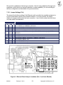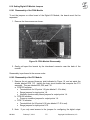
1
878 DIOD Distributed Input/Output Device Manual February 7, 2013 ML0041 Document Revision A © 2013 by Bitronics, LLC TABLE OF CONTENTS FIRMWARE VERSION ....................................................................................................................................... v M87x MANUAL SET .......................................................................................................................................... v INSTALLATION AND MAINTENANCE ............................................................................................................vi WARRANTY AND ASSISTANCE .....................................................................................................................vi AUTHORIZED REPRESENTATIVE IN THE EUROPEAN UNION .................................................................vii COPYRIGHT NOTICE ......................................................................................................................................vii TRADEMARKS ................................................................................................................................................vii SAFETY SECTION ............................................................................................................................................ix 1.0 DESCRIPTION ............................................................................................................................................ 1 1.1 Introduction .............................................................................................................................................. 1 1.2 Features .................................................................................................................................................. 1 1.3 Specifications .......................................................................................................................................... 1 1.4 Standards and Certifications ................................................................................................................... 5 1.4.1 Environment ..................................................................................................................................... 5 2.0 HOUSING AND BACKPLANE ................................................................................................................... 7 2.1 2.2 2.3 2.4 2.5 2.6 2.7 Installation .............................................................................................................................................10 Initial Inspection.....................................................................................................................................10 Protective Ground/Earth Connections...................................................................................................10 Instrument Mounting..............................................................................................................................10 Surge Protection....................................................................................................................................10 Cleaning ................................................................................................................................................10 Removal and Installation of Modules ....................................................................................................11 3.0 HOST PROCESSOR MODULE H12 ........................................................................................................12 3.1 Host board .............................................................................................................................................12 3.1.1 Serial Port/Front Panel Board ........................................................................................................12 3.1.1a Service Port (P1) .....................................................................................................................12 3.1.1b Standard Serial Ports (P2, P3, P4) ..........................................................................................13 3.1.1c Diagnostic Status LED’s (S1, S2, S3, S4) ...............................................................................14 3.1.1d RS485 Connections .................................................................................................................14 3.1.2 Self-Test Modes .............................................................................................................................20 3.1.3 System Clock .................................................................................................................................21 4.0 MEASUREMENTS ....................................................................................................................................22 4.1 List of Available Measurements ............................................................................................................22 5.0 FUNCTIONAL DESCRIPTION ..................................................................................................................23 5.1 Passwords .............................................................................................................................................23 5.2 Configuration .........................................................................................................................................23 5.3 Triggering ..............................................................................................................................................24 5.3.1 Digital Input Trigger ........................................................................................................................24 5.3.2 Edge and Level Triggers ................................................................................................................25 5.3.3 Manual Trigger ...............................................................................................................................25 5.3.4 Logical Combinations of Triggers ..................................................................................................25 5.3.5 Cross Triggering Multiple 70 Series Units (Inter-triggering) ..........................................................25 5.3.6 Periodic Triggers ............................................................................................................................26 5.4 Sequence of Events (SOE) File .............................................................................................................27 5.5 878 File System .....................................................................................................................................27 5.5.1 FTP Server .....................................................................................................................................28 5.5.1a Introduction to FTP ..................................................................................................................28 5.5.1b 878 FTP Implementation .........................................................................................................29 5.5.2 Zmodem, TELNET, and Command Line Interface ........................................................................29 ML0041 February 7, 2013 ii Copyright 2013 Bitronics, LLC 5.6 IRIG-B ...................................................................................................................................................30 5.6.1 Overview ........................................................................................................................................30 5.6.2 Introduction to IRIG Standards ......................................................................................................30 5.6.2a Time Code Format (Rate Generation) .....................................................................................31 5.6.2b Format Designation .................................................................................................................31 5.6.2c Carrier/Resolution ....................................................................................................................31 5.6.2d Coded Expressions .................................................................................................................32 5.6.3 878 IRIG-B Implementation ...........................................................................................................32 5.6.3a 878 IRIG-B Receiver ...............................................................................................................32 5.6.3b 878 IRIG-B Decoder ................................................................................................................32 5.6.3c 878 IRIG-B Time Qualifier .......................................................................................................32 5.6.4 Determining the Correct Year ........................................................................................................33 5.6.5 Methods of Automatic Clock Adjustments .....................................................................................34 5.6.6 Types of 878 Clock Synchronization .............................................................................................34 5.6.6a Frequency Adjustments and Free Wheeling ...........................................................................34 5.6.6b Permanent IRIG-B Source Connection ...................................................................................34 5.6.7 Stages of IRIG-B Synchronization and Accuracy ..........................................................................35 5.6.7a Power-Up Stage ......................................................................................................................35 5.6.7b Time Lock Stage ......................................................................................................................35 5.6.7c Frequency Lock Stage .............................................................................................................35 5.6.7d Final Lock Stage ......................................................................................................................36 5.6.8 Notes On Operation .......................................................................................................................36 5.6.9 IRIG-B Electrical Specifications .....................................................................................................36 5.6.10 IRIG-B Port Wiring Instructions (Pulse Width Coded, IRIG-B master, .........................................36 Demodulated)...........................................................................................................................................36 5.6.11 Modulated IRIG-B .........................................................................................................................37 5.6.12 Setup Instructions for Use of the M87x Modulated IRIG-B Converter (Sine ................................37 Wave, Amplitude Modulated, IRIG-B master) ..........................................................................................37 5.7 Time Sync & Setting .............................................................................................................................37 5.7.1 Time Sync Status Registers .........................................................................................................38 5.7.2 Manual time setting by Command-Line instruction .....................................................................38 5.7.3 Unsolicited DNP Time set (DNP master sets the IED clock) ......................................................38 5.7.4 IRIG-B Time sync (time-synchronization via dedicated IED port) ..............................................38 5.7.5 (UCA) Network Time Synchronization - time synchronization over Ethernet .............................39 5.7.6 SNTP (Simple Network Time Protocol) - time synchronization over Ethernet ...........................39 5.7.7 DNP Time sync (slave requesting DNP time be set) ..................................................................39 5.8 Automatic Event Notification .................................................................................................................39 5.8.1 Email Notifications .........................................................................................................................40 5.8.2 Serial Notifications .........................................................................................................................40 5.8.3 Data Sent .......................................................................................................................................40 5.8.4 Error Recovery ...............................................................................................................................40 5.8.5 Example .........................................................................................................................................40 5.8.6 Control Characters ..........................................................................................................................40 6.0 POWER SUPPLY V10 ..............................................................................................................................42 6.1 Introduction ............................................................................................................................................42 6.2 Features ................................................................................................................................................42 6.3 Specifications ........................................................................................................................................42 6.3.1 Environmental ................................................................................................................................43 6.3.2 Physical ..........................................................................................................................................43 6.4 Power Supply and Protective Ground (Earth) Connections ..................................................................44 6.5 Overcurrent Protection ..........................................................................................................................44 6.6 Supply/Mains Disconnect ......................................................................................................................44 7.0 ETHERNET MODULE P10, P11, P12 OR E1, E3 OPTION WITH H12 HOST ........................................45 7.1 7.2 7.3 7.4 7.5 Introduction ............................................................................................................................................45 Features ................................................................................................................................................46 Specifications (For P1x Modules Unless Otherwise Noted) .................................................................46 Environmental .......................................................................................................................................47 Physical .................................................................................................................................................47 ML0041 February 7, 2013 iii Copyright 2013 Bitronics, LLC 7.6 Hot Swap (HS) Compatibility (P1x Modules) ........................................................................................47 7.7 Hardware Configuration ........................................................................................................................47 7.8 Cabling ..................................................................................................................................................48 7.9 Connections ..........................................................................................................................................48 7.10 Troubleshooting the Connection .........................................................................................................48 7.11 Indicators .............................................................................................................................................48 7.12 Software Configuration ........................................................................................................................49 7.13 Technical Details .................................................................................................................................49 7.13.1 Jumper Settings (P1x) .................................................................................................................50 7.13.2 Troubleshooting ...........................................................................................................................51 7.13.3 PHYSTS Register Contents (P1x) ...............................................................................................52 7.13.4 Statistics Gathered by Ethernet Driver ........................................................................................53 8.0 DIGITAL INPUT / OUTPUT MODULE P30A, P31 ...................................................................................54 8.1 Introduction ............................................................................................................................................54 8.2 Features ................................................................................................................................................54 8.3 Specifications ........................................................................................................................................55 8.4 Environmental .......................................................................................................................................56 8.5 Physical .................................................................................................................................................56 8.6 Hot Swap (HS) Compatibility .................................................................................................................56 8.7 Description .............................................................................................................................................56 8.7.1 P30A ...............................................................................................................................................56 8.7.2 P31 .................................................................................................................................................57 8.8 System Design Considerations .............................................................................................................57 8.8.1 Input / Output Impedance ...............................................................................................................57 8.8.2 Input Assignments .........................................................................................................................57 8.9 Debounce Time Setting .........................................................................................................................57 8.10 Setting Digital I/O Module Jumpers.....................................................................................................61 8.10.1 Disassembly of the P30A Module ................................................................................................61 8.10.2 Disassembly of the P31 Module ..................................................................................................61 TM 8.10.3 CompactPCI Interface Board (692) Jumper Settings ...............................................................62 8.10.4 I/O Board (693) Jumper Settings .................................................................................................63 8.10.5 Health Status Digital Output Setting (Optional assignment of Digital Output 1 of Module 0) ......65 9.0 TRANSDUCER INPUT MODULE P40......................................................................................................66 9.1 Introduction ............................................................................................................................................66 9.2 Features ................................................................................................................................................67 9.3 Specifications ........................................................................................................................................68 9.4 Environmental .......................................................................................................................................68 9.5 Physical .................................................................................................................................................69 9.6 Hot Swap (HS) Compatibility .................................................................................................................69 9.7 Description .............................................................................................................................................69 9.8 System Design Considerations .............................................................................................................69 9.8.1 Input Type Jumper Settings ...........................................................................................................69 9.8.2 Transducer Input Scaling Configuration ........................................................................................71 9.8.3 Setting the Data Update Rate (Poll rate) for P40 Transducer Inputs ............................................71 Appendix A - Cross Triggering .....................................................................................................................73 Appendix B - Firmware Version History .......................................................................................................87 ML0041 February 7, 2013 iv Copyright 2013 Bitronics, LLC FIRMWARE VERSION The following table provides the most recent firmware and software versions. For best results, the Configurator version used should match with the firmware version. A complete list of firmware and software versions is provided on the 70 Series Utilities CD. Firmware Versions Description M870 Family 878 Product Release: New H12 Host Processor with and without E1 and E3 Ethernet options Bios Version DSP Firmware Host Firmware Configurator Utilities CD N/A 1.33 4.01 4.01 4.01 Release Date 12/13/12 M87X MANUAL SET ML0021 ML0025 ML0026 ML0027 ML0034 ML0041 ML0041 M87x User Manual 70 SERIES Modbus Protocol 70 SERIES DNP3 Protocol M870D Remote Display Manual 70 SERIES IEC61850® Protocol Manual 878 DIOD User Manual February 7, 2013 v Copyright 2013 Bitronics, LLC INSTALLATION AND MAINTENANCE Bitronics LLC products are designed for ease of installation and maintenance. As with any product of this nature, installation and maintenance can present electrical hazards and should be performed only by properly trained and qualified personnel. If the equipment is used in a manner not specified by Bitronics LLC, the protection provided by the equipment may be impaired. In order to maintain UL recognition, the following Conditions of Acceptability shall apply: a) Terminals and connectors that shall be connected to live voltages are restricted to nonfield wiring applications only. b) After installation, all hazardous live parts shall be protected from contact by personnel or enclosed in a suitable enclosure. WARRANTY AND ASSISTANCE This product is warranted against defects in materials and workmanship for a period of one hundred and twenty (120) months from the date of their original shipment from the factory. Products repaired at the factory are likewise warranted for eighteen (18) months from the date the repaired product is shipped, or for the remainder of the product's original warranty, whichever is greater. Obligation under this warranty is limited to repairing or replacing, at our designated facility, any part or parts that our examination shows to be defective. Warranties only apply to products subject to normal use and service. There are no warranties, obligations, liabilities for consequential damages, or other liabilities on the part of Bitronics LLC except this warranty covering the repair of defective materials. The warranties of merchantability and fitness for a particular purpose are expressly excluded. For assistance, contact Bitronics LLC at: Telephone: Fax: Email: Website: 610.997.5100 610.997.5450 [email protected] www.novatechweb.com/bitronics Shipping: 261 Brodhead Road Bethlehem, PA 18017-8698 USA ML0041 February 7, 2013 vi Copyright 2013 Bitronics, LLC AUTHORIZED REPRESENTATIVE IN THE EUROPEAN UNION NovaTech Europe BVBA Kontichsesteenweg 71 2630 Aartselaar Belgium T +32.3.458.0807 F +32.3.458.1817 E [email protected] COPYRIGHT NOTICE This manual is copyrighted and all rights are reserved. The distribution and sale of this manual is intended for the use of the original purchaser or his agents. This document may not, in whole or part, be copied, photocopied, reproduced, translated or reduced to any electronic medium or machine-readable form without prior consent of Bitronics LLC, except for use by the original purchaser. The product described by this manual contains hardware and software that is protected by copyrights owned by one or more of the following entities: Bitronics LLC, 261 Brodhead Road, Bethlehem, PA 18017; Ardence, Inc., Five Cambridge Center, Cambridge, MA 02142; SISCO, Inc., 6605 19½ Mile Road, Sterling Heights, MI 48314-1408; General Software, Inc., Box 2571, Redmond, WA 98073; Schneider Automation, Inc., One High Street, North Andover, MA 01845; Triangle MicroWorks, Inc., 2213 Middlefield Court, Raleigh, NC 27615 Greenleaf Software Inc., Brandywine Place, Suite 100, 710 East Park Blvd, Plano, TX 75074 TRADEMARKS The following are trademarks or registered trademarks of Bitronics LLC: The Bitronics logo Bitronics PowerPlex Triplex Triple-II MultiComm PowerServe SubCycle Technology SubCycleStuf The following are trademarks or registered trademarks of AREVA T&D Inc. AREVA T&D the AREVA logo MiCOM The following are trademarks or registered trademarks of the DNP User's Group: DNP DNP3 The following are trademarks or registered trademarks of the Electric Power Research Institute (EPRI): UCA. UCA2 The following are trademarks or registered trademarks of Schneider Automation, Inc.: MODSOFT Modicon Modbus Plus Modbus Compact 984 PLC The following are trademarks or registered trademarks of Ardence, Inc.: ML0041 February 7, 2013 vii Copyright 2013 Bitronics, LLC Phar Lap the Phar Lap logo The following are trademarks or registered trademarks of Systems Integration Specialists Company, Inc. (SISCO): SISCO MMS-EASE Lite AX-S4MMS The following are trademarks or registered trademarks of General Software, Inc.: General Software the GS logo EMBEDDED BIOS Embedded DOS The following are trademarks or registered trademarks of the PCI Industrial Computer Manufacturers Group: CompactPCI PICMG the CompactPCI logo the PICMG logo ML0041 February 7, 2013 viii Copyright 2013 Bitronics, LLC SAFETY SECTION This Safety Section should be read before commencing any work on the equipment. Health and safety The information in the Safety Section of the product documentation is intended to ensure that products are properly installed and handled in order to maintain them in a safe condition. It is assumed that everyone who will be associated with the equipment will be familiar with the contents of the Safety Section. Explanation of symbols and labels The meaning of symbols and labels that may be used on the equipment or in the product documentation is given below. Installing, Commissioning and Servicing Equipment connections Personnel undertaking installation, commissioning or servicing work on this equipment should be aware of the correct working procedures to ensure safety. The product documentation should be consulted before installing, commissioning or servicing the equipment. Terminals exposed during installation, commissioning and maintenance may present a hazardous voltage unless the equipment is electrically isolated. If there is unlocked access to the equipment, care should be taken by all personnel to avoid electric shock or energy hazards. ML0041 February 7, 2013 ix Copyright 2013 Bitronics, LLC Voltage connections should be made using insulated crimp terminations to ensure that terminal block insulation requirements are maintained for safety. To ensure that wires are correctly terminated, the correct crimp terminal and tool for the wire size should be used. Before energizing the equipment, it must be grounded (earthed) using the protective ground (earth) terminal, or the appropriate termination of the supply plug in the case of plug connected equipment. Omitting or disconnecting the equipment ground (earth) may cause a safety hazard. The recommended minimum ground (earth) wire size is 2.5 mm2 (#12 AWG), unless otherwise stated in the technical data section of the product documentation. Before energizing the equipment, the following should be checked: 1. Voltage rating and polarity 2. Protective fuse rating 3. Integrity of ground (earth) connection (where applicable) 4. Equipment operating conditions The equipment should be operated within the specified electrical and environmental limits. Insulation and dielectric strength testing Insulation testing may leave capacitors charged up to a hazardous voltage. At the end of each part of the test, the voltage should be gradually reduced to zero, to discharge capacitors, before the test leads are disconnected. Removal and insertion of modules All M87x active circuitry is located on removable modules. Unless a Module is specifically intended for Hot Swap (see documentation), it must not be inserted into or withdrawn from equipment while it is energized, since this may result in damage. Hot Swap modules may be installed and removed under power. Refer to the appropriate section or manual to determine if the particular module is Hot Swap compatible. For all other modules, remove all power from the unit before installing or removing any module. All Hazardous Voltages MUST be removed from the 878 before removing or installing the Power Supply Module. All connections to a module must be removed before removing the module. Do not attempt to install a module with signals connected. Fiber optic communication Where fiber optic communication devices are fitted, these should not be viewed directly. Optical power meters should be used to determine the operation or signal level of the ML0041 February 7, 2013 x Copyright 2013 Bitronics, LLC device. WARNING: EMISSIONS – CLASS A DEVICE (EN55011) This is a Class A industrial device. Operation of this device in a residential area may cause harmful interference, which may require the user to take adequate measures. DECOMMISSIONING AND DISPOSAL 1. Decommissioning The auxiliary supply circuit in the equipment may include capacitors across the supply or to ground (earth). To avoid electric shock or energy hazards, after completely isolating the supplies to the relay (both poles of any dc supply), the capacitors should be safely discharged via the external terminals before decommissioning. 2. Disposal It is recommended that incineration and disposal to watercourses is avoided. The product should be disposed of in a safe manner. Any products containing batteries should have them removed before disposal, taking precautions to avoid short circuits. Particular regulations within the country of operation may apply to the disposal of lithium batteries. ML0041 February 7, 2013 xi Copyright 2013 Bitronics, LLC 1.0 DESCRIPTION 1.1 Introduction The 878 Distributed Input/Output Device (DIOD) is derived from Bitronics M87x. It combines a modular-by-board chassis featuring a CompactPCITM card cage and a 486based host processor. 1.2 Features Simultaneous support of multiple protocols over multiple physical links 486-class Host processor. Watchdog timer maximizes system reliability. 4 Configurable serial ports - Three RS232/RS485 ports and one DB9M Service RS232 port Fully compatible CompactPCITM backplane and system bus. Rugged all-aluminum housing. Choice of standard chassis (C07A5) with 3 option cPCI expansion bays, intermediate chassis (C10A7) with 5 option bays or extended model (C12A8) with 6 option bays. Option modules include digital I/O (P30A and P31), Ethernet (E1, E3), and transducer input (P40) 1.3 Specifications Power Supply Input Voltage Nominal: 24-250Vdc, 69-240Vac (50/60Hz) Operating Range: 20-300Vdc, 55-275Vac (45-65Hz) Burden: 50VA max, 20W max (C07A5) 70VA max, 25W max (C12A8 and C10A7) ML0041 February 7, 2013 1 Copyright 2013 Bitronics, LLC Operating Temperature Relative Humidity Installation Category Pollution Degree Enclosure Protection Altitude Intended Use -40C to 70C 0-95% non-condensing IC III (Distribution Level) Refer to definitions below. Pollution Degree 2 Refer to definitions below. IP20 to IEC60529:1989 Up to and including 2000m above sea level Indoor use; Indoor/Outdoor use when mounted in an appropriately rated protective enclosure to NEMA or IP protection classifications, as required for the installation. Inputs 0 – 10V Voltage Range 0 – 1mA Current Range 4 – 20mA Current Range Common Mode Input Range Common Mode Error Accuracy Protection Data Update Rate (Poll Rate) Input / Output Capacitance, any Terminal to Case ML0041 Environmental February 7, 2013 -P40 Transducer Input Module 8 bi-directional, jumper selectable for voltage or current range. Overload Range: -12.5 V to +12.5 Vdc Resolution: 0.381 mV Input Resistance: 10KΩ Overload Range: -2.5 mA to +2.5 mA Resolution: 0.0763 μA Input Resistance: 500Ω Overload Range: 0 mA to +25 mA Resolution: 0.381 μA Input Resistance: 50Ω +/- 9V, Input to Chassis Vcm DC 0.3% of FS @ 9Vp Common Mode Vcm 50/60Hz 0.1% of FS @ 9Vp Common Mode AC 0.25% of Full Scale Input Input terminals have internal transzorb clamp and 90V spark gap protection. 100ms minimum (single P40 module); 500ms minimum (multiple P40 modules) 470pF 2 Copyright 2013 Bitronics, LLC Power Supply Requirements Hot Swap Connections Package ML0041 February 7, 2013 -P40 Transducer Input Module 3.3Vdc, 5Vdc, +/-12Vdc (supplied from backplane) Complies with Hot Swap specification PICMG 2.1 R1.0 for Basic Hot Swap (requires Host Processor re-boot) Removable Terminal Blocks, accepts #16-28AWG (1,4-0,09mm) wire. Recommended Torque Rating is 2.2 In-Lbs, 0.25 N-m. Standard 0.150" (3,81mm) header socket accepts other standard terminal types. Solid core wire is recommended, or stranded wire with the use of “bootlace ferrules,” where these are available. CompactPCITM (3U, 4HP) removable module 3 Copyright 2013 Bitronics, LLC Definitions: Installation Category (Overvoltage Category) III: Distribution Level, fixed installation, with smaller transient overvoltages than those at the primary supply level, overhead lines, cable systems, etc. Pollution: Any degree of foreign matter, solid, liquid, or gaseous that can result in a reduction of electric strength or surface resistivity of the insulation. Pollution Degree 2: Only non-conductive pollution occurs except that occasionally a temporary conductivity caused by condensation is to be expected. ML0041 February 7, 2013 4 Copyright 2013 Bitronics, LLC 1.4 Standards and Certifications 1.4.1 Environment UL/CSA Recognized, File Number E164178 UL61010-1, 2nd edition (July 12, 2004; revision date 2008-10-28) CAN/ CSA No. 61010-1-04 (2nd edition, dated July 12, 2004) If applicable, the CE mark must be prominently marked on the case label. European Community Directive on EMC 2004/108/EC, (replaced former directive 89/336/EEC amended by 92/31/EEC, 93/68/EEC, 98/13/EC), and Directive 91/263/EC [TTE/SES]. European Community Directive on Low Voltage 73/23/EEC 2006/95/EC (replaces former Directive 73/23/EEC) Product and Generic Standards The following product and generic standards were used to establish conformity: Low Voltage (Product Safety): EN 61010-1: 2001 EMC: EN 61326-1: 2006, EN60255-26:2006 (supersedes EN 50263: 2000), EN 61000-6-2: 2005, EN 61000-6-4: 2007/A1:2011 (IEC date 2010), (EN 50081-2: 1993, EN 50082-2: 1995 have been superseded). Radiated Emissions Electric Field Strength EN 60255-25: 2000 / EN55011: 2009/A1:2010 (supersedes EN55011:2007/ A2: 2007 which superseded EN55011: 1998 / A1: 1999/A2 : 2002) Group 1, Class A Frequency: 30 - 1000 MHz AC Powerline Conducted Emissions EN 60255-25:2000 / EN55011: 2009/A1:2010 (supersedes EN55011 2007/ A2: 2007 which superseded EN55011: 1998 / A1: 1999/A2 : 2002) Group 1, Class A Frequency: 150 kHz – 30 MHz 1 MHz Burst Disturbance Test IEC60255-22-1: 1988 Class III Amplitude: 2.5 kV Electrostatic Discharge (ESD) EN61000-4-2: 2009 (supersedes EN 61000-4-2: 1995 / A1:1998 / A2: 2001) Discharge voltage: ± 8 KV Air; ± 4 KV Contact (Additionally meets ± 6kv Contact) Immunity to Radiated Electromagnetic Energy (Radio-Frequency) EN61000-4-3:2006 /A1:2008/A2:2010, Class III (Supersedes IEC 61000-4.3: 1995 & EN61000-4-3: 2002 / A1:2002; and ENV 50204: 1996, on Immunity to Radiated Electromagnetic Energy -Digital Radio Telephones 900 MHz & 1890 MHz). Frequency: 80 –1000 MHz Amplitude: 10.0 V/m Modulation: 80% AM @ 1kHz ML0041 February 7, 2013 5 Copyright 2013 Bitronics, LLC Frequency: 1400-2000 MHz Frequency: 2000-2700 MHz Amplitude: 3.0 V/m Amplitude: 1.0 V/m Digital Radio Telephones Frequency: 900 MHz/1890 MHz Amplitude: 10.0/3.0 V/m Modulation: 80% AM @ 1kHz Modulation: 80% AM @ 1kHz Modulation: 80% AM @ 1kHz Electrical Fast Transient / Burst Immunity EN 61000-4-4: 2004/A1:2010 (supersedes IEC61000-4-4: 1995) Burst Frequency: 5 kHz Amplitude, Input AC Power Ports: Severity Level 4; Amplitude ± 4 kV Amplitude, Signal Ports: Severity Level 3; Amplitude ± 2 kV Amplitude, Telecom Ports (Ethernet): ± 1 kV Current/Voltage Surge Immunity EN 61000-4-5: 2006 (supersedes IEC61000-4-5: 1995, EN610000-4-5: 1995/A1:2001) Installation Class: 3 Open Circuit Voltage: 1.2 / 50 µs Short Circuit Current: 8 /20 µs Amplitude: 2 kV common mode, 1 kV differential mode Immunity to Conducted Disturbances Induced by Radio Frequency Fields EN 61000-4-6: 2009 (supersedes EN 61000-4-6: 2007 which superseded IEC61000-4-6: 1996, EN 61000-4-6: 1996 / A1:2001) Level: 3 Frequency: 150 kHz – 80 MHz Amplitude: 10 VRMS Modulation: 80% AM @ 1kHz Power Frequency Magnetic Fields EN61000-4-8:2010 Amplitude: 30 A/m Frequency: 50 and 60 Hz AC Supply Voltage Dips and Short Interruptions EN 61000-4-11: 2004 (supersedes IEC61000-4-11: 1994) Duration: 10ms on auxiliary power supply, under normal operating conditions, without deenergizing. Surge Withstand Capability Test For Protective Relays and Relay Systems ANSI/IEEE C37.90.1: 1989 Vibration IEC60255-21-1: 1988 Endurance Class: 1 Shock and Bump IEC60255-21-2: 1988 Bump Class: 1 ML0041 February 7, 2013 6 Copyright 2013 Bitronics, LLC 2.0 HOUSING AND BACKPLANE The 878 chassis is a modular-by-board design, with a rugged aluminum housing specifically designed to meet the harsh conditions found in utility and industrial applications. The chassis features a passive backplane, an embedded and fully compatible CompactPCITM (cPCI) bus. All active circuitry is located on removable modules. There are three types of modules: Power Supply, the Host Processor, and cPCI expansion modules. See Figure 1 (below) for the locations of the module bays in the standard chassis. Figure 1 - Front View and Module Assignment (C07A5, M871 Shown, no signal input or DSP on 878) The power supply bay utilizes a standard cPCI power connector. The Host Processor and the cPCI expansion bays have standard cPCI connectors. The expansion bays are fully compatible, both electrically and mechanically with cPCI standards. The Backplane board is an eight-layer circuit board, and contains a 5V, 33MHz cPCI bus. The standard bay assignment for the standard chassis (C07A5) is shown above. The 878 is also available in an intermediate chassis (C10A7) that adds two additional cPCI expansion bays, and an extended chassis, (C12A8) that adds three additional cPCI expansion bays. The H12 host processor with either of the combined Ethernet options (E1 or E3) as shown uses a wider front plate incorporating the first of the expansion slots to the left of the host/Ethernet module. ML0041 February 7, 2013 7 Copyright 2013 Bitronics, LLC Figure 2 - Mounting and Overall Dimensions (C07A5) ML0041 February 7, 2013 8 Copyright 2013 Bitronics, LLC 13.45" (342) ø 0.25" 2.33" (59) 5.20" (132) 2.33" (59) 0.27" (6.9) 13.00" (330) 0.23" (5.7) Figure 3 - Mounting and Overall Dimensions (C12A8 and C10A7) ML0041 February 7, 2013 9 Copyright 2013 Bitronics, LLC 2.1 Installation WARNING - INSTALLATION AND MAINTENANCE SHOULD ONLY BE PERFORMED BY PROPERLY TRAINED OR QUALIFIED PERSONNEL. 2.2 Initial Inspection Bitronics instruments are carefully checked and "burned in" at the factory before shipment. Damage can occur however, so please check the instrument for shipping damage as it is unpacked. Notify Bitronics LLC immediately if any damage has occurred, and save any damaged shipping containers. 2.3 Protective Ground/Earth Connections There are two chassis ground points that MUST be connected to Earth Ground (refer to Figure 8, pg. 68). The first is the Protective Ground (Earth) terminal (terminal 2) on the Power Supply input. The minimum Protective Ground (Earth) wire size is 2.5 mm2 (#12 AWG). The second is the mounting flange. Bitronics LLC recommends that all grounding be performed in accordance with ANSI/IEEE C57.13.3-1983. 2.4 Instrument Mounting The unit should be mounted with four #10-32 (M4) screws. Make sure that any paint or other coatings on the panel do not prevent electrical contact. The device is intended to be connected to earth ground at the mounting plate. See Section 2.3. 2.5 Surge Protection Surge protection devices are incorporated into the power supply. See Section 2.3 for grounding/earthed recommendations. If the unit is to be powered from a VT, it is recommended that one side of the VT be grounded at the instrument following ANSI/IEEE C57.13.3-1983. See Section 6.5 for fuse recommendations. 2.6 Cleaning Cleaning the exterior of the instrument shall be limited to the wiping of the instrument using a soft damp cloth applicator with cleaning agents that are not alcohol based, and are nonflammable and non-explosive. ML0041 February 7, 2013 10 Copyright 2013 Bitronics, LLC 2.7 Removal and Installation of Modules All active circuitry is located on removable modules. Hot Swap modules may be installed and removed under power. Refer to the appropriate section or manual to determine if the particular module is Hot Swap compatible. For all other modules, remove all power from the unit before installing or removing any module. All Hazardous Voltages MUST be removed from the 878 before removing or installing the Power Supply Module. The Signal Input Module and the Power Supply may be withdrawn from the housing after removal of the front panel screws. All connections to a module must be removed before removing the module. Do not attempt to install a module with signals connected. To remove a cPCI module, use the following procedure: 1. 2. 3. 4. 5. 6. Remove power from the unit (except Hot Swap modules). Unscrew the M2.5 Phillips front panel screws (note that these are captive screws). The screw in the handle has been left out intentionally. Pull the red sliding release tab up and outward until handle is unlocked. Push the handle downward (when viewed from the front) to lever out the module. Once the module is disengaged from the backplane connector, carefully withdraw the module. Be extremely careful when handling the module, especially the backplane connector. To insert a cPCI module, use the following procedure: 1. 2. 3. 4. Make sure the red sliding release tab is fully extended from the handle, and that the handle is in the downward position (when viewed from the front). Line up the module with the card guides in the appropriate position (the Host/Analog-Digital Signal Processor Module MUST be inserted in the right most double width bay). Use the handle to lever the module into the housing. When the module is fully engaged, tighten the M2.5 Phillips front panel screws. The screw in the handle has been left out intentionally. ML0041 February 7, 2013 11 Copyright 2013 Bitronics, LLC 3.0 HOST PROCESSOR MODULE H12 3.1 Host board The Host CPU module consists of a 486-class microprocessor, four communications ports and a CompactPCITM master bridge. The H12 host module utilizes a Compact Flash card, and offers optional Ethernet interfaces (E1 and E3). 3.1.1 Serial Port/Front Panel Board The Serial Port/Front Panel Board consists of the four serial driver connectors, four status LED’s, four bi-color serial port LED’s, and a reset button. Port P1 is a PC-AT style 9-pin D connector for the dedicated RS-232 port, and ports P2, P3, and P4 are universal 150-mil, 6-pin removable connectors for the RS-232/RS-485 serial ports. P2, P3, and P4 are software (user) configurable for RS-232 or RS-485 mode. The RS-232 drivers support full and half duplex modes. See Figures 3-6 (pg. 20 -24) for signal assignments. 3.1.1a Service Port (P1) When connecting to the Service port DB9M (P1) from a PC, a null modem cable is required. The Service Port can be used with a PC running a terminal emulation program. Upon startup, the 878 default configuration sets P1 for 9600 baud, 8 data bits, no parity, 1 stop bit and no flow control handshaking. These parameters are user-configurable. A small number of messages are sent to P1 and the 878 then outputs system messages. Enter the command mode by pressing the ENTER key until the system outputs a prompting message. Allowable commands are: Service Port\Zmodem Commands c: dir receive time cd exit reset type chp1 getlog router trigger dr1 chp2 Goose* send trigger dr2 d: ip serial trigger wv1 date mac setlog trigger wv2 del nsap subnet ver dio point password software whoami display on pulse receive vio point display off reboot status Note: * This command is for UCA Goose only and is now referred to as GSSE. Type “help <command>” to find out more about a particular command. commonly used commands are: The more ip - Set Internet Protocol (IP) address information in "dotted decimal" format. The IP address defaults to "192.168.0.254". subnet – Set the Subnet mask. The Subnet mask defaults to "255.255.255.0". ML0041 February 7, 2013 12 Copyright 2013 Bitronics, LLC router – Set the Gateway (Router) address. The Gateway (Router) address defaults to "192.168.0.1". nsap - Set the OSI network address (NSAP) in "space delimited octet string" format. The default address is "49 00 01 42 49 09 01 01" which is a local address not attached to the global OSI network. The correct value for your network should be obtained from the network administrator. The default values are valid for a device that is attached to a local intranet with optional access via a router (such as a device within a substation). time - Set the time as 24-hour UTC time. Time is entered as HH:MM:SS. The factory default is set to GMT. date – Set the date. Date is entered as MM/DD/YYYY. serial - Display M87x serial number exit - Exit command line mode and return to logging mode. If no commands are received for five minutes the device will revert to logging mode. 3.1.1b Standard Serial Ports (P2, P3, P4) These ports can be set to RS-232 or RS-485, and support baud rates up to 115200. Setup of the Serial Ports can be accomplished by using the 70 Series Configurator. The default configuration for the serial ports is: Serial Port Default Settings Port Protocol Parity Baud IED Address Physical Media P1 Zmodem/Display/Log None 9600 P2 DNP 3.0 None 9600 1 RS-232 P3 Modbus Even 9600 1 RS-232 P4 Zmodem/Display/Log None 9600 RS-232 RS-232 The configuration of these ports is stored internally in the "COMM.INI" file (Section 5.2). If, for any reason, the configuration of the serial ports is erroneously set, the factory default settings can be restored by using FTP. The file "COMM.INI" can be deleted, which will return all ports to the factory default setting. The settings can then be changed by using the 70 Series Configurator. Host cable requirements for CE compliance: On ports P2, P3, and P4, as well as a port that utilizes the externally mounted M87x Modulated IRIG-B Converter, install snap-on ferrite (Fair-Rite #0461164181 or equivalent) onto each cable by wrapping the cable through the ferrite opening two times before snapping the ferrite closed. Tie RS-485 cable shields (pin 5) to earth ground at one point in system. The recommended torque rating for the terminal block wire fasteners on ports P2-P4 ML0041 February 7, 2013 13 Copyright 2013 Bitronics, LLC is 2.2 In-Lbs, 0.25 N-m. 3.1.1c Diagnostic Status LED’s (S1, S2, S3, S4) There are four LED’s on the front panel: S1, S2, S3, and S4. They perform the following functions: LED S1 Description On while flash memory is being written to, otherwise off. S2 Flashes every 5 power-line cycles, indicates DSP operating properly. S3 On while CPU is busy. Intensity indicates CPU utilization level. S4 On during internal self-diagnostics after boot-up. 3.1.1d RS485 Connections Note that various protocols and services have different port connection requirements. When making connections to serial ports for Modbus or DNP3 over RS485, 2-wire half duplex is required. This is because it is necessary to maintain a minimum time period (3 1/3 characters) from the time the transmitter shuts off to the next message on the bus in order to guarantee reliable communications. However, when using Zmodem or connecting to the remote display, asynchronous 2 way communications are required, and therefore a 4-wire full duplex (technically RS422) connection is needed. See figure 6 below for RS485 cable wiring diagrams showing both 2 and 4 wire. There are special considerations for multi-drop Zmodem connections. Zmodem protocol was developed for RS232 point-to-point connections so it does not support any standard convention for addressing. Therefore, it does not facilitate multi-drop communications buses. In order to make it possible to use one modem to establish remote communications with multiple 70 Series devices when the Ethernet option (preferred) is not fitted, the following proprietary convention is employed. When using HyperTerminal or a dial-up modem with RS485, the port on the IED must be configured for "Zmodem" protocol, not for "Zmodem/Display/Log". This is done with the pull-down menu in the Configurator program, see illustration below. Selecting Zmodem also enables an address to be set for the selected COM port. When daisy-chaining multiple devices on RS485, each device must have a unique address. ML0041 February 7, 2013 14 Copyright 2013 Bitronics, LLC Type the command "connect 01" (use the actual address assigned) to establish communications with the device in Zmodem protocol using RS485. This command will not be echoed back as you type it. After striking the enter key, the device will return a command prompt (for example c:\>, e:\data>, c:\config>, etc.) Once communications are established, you can now use the command-line interface, exactly as you would with a direct RS232 connection, to control the device (services supported by Zmodem protocol include: download recording files, control digital outputs, reset demands, set time and date, etc.). In order to disconnect from one device and connect to another on the same bus, type the command "exit" to end the session then type “connect 02” (or whatever address you want to connect to). ML0041 February 7, 2013 15 Copyright 2013 Bitronics, LLC Figure 3 - Typical RS-232 & IRIG-B Cable Wiring ML0041 February 7, 2013 16 Copyright 2013 Bitronics, LLC Figure 4 - Typical RS-485 Cable Wiring ML0041 February 7, 2013 17 Copyright 2013 Bitronics, LLC Figure 5 – M870D RS-232 Cable Wiring ML0041 February 7, 2013 18 Copyright 2013 Bitronics, LLC Figure 6 - Host Port Signal Assignment ML0041 February 7, 2013 19 Copyright 2013 Bitronics, LLC 3.1.2 Self-Test Modes The M87x has several self-tests built in to assure that the instrument is performing accurately. Refer to the appropriate protocol manual for details on how to retrieve the self-test information. The following table lists possible faults that would be detected by the self-tests, how the fault is indicated, the effects of the fault and any necessary corrective actions. Bit # Description Self-Test Bits Hardware Effect Default Value 0(LSB) Factory gain calibration of Analog-Digital Signal Processor Module checksum error. A10 EEProm Unit will continue to function using default values, at reduced accuracy. A/D Gain = 1 1 Factory offset calibration of Analog-Digital Signal Processor Module checksum error. A10 EEProm Unit will continue to function using default values, at reduced accuracy. A/D Offset = 0 2 Factory gain calibration of Signal Input Module checksum error. S1x EEProm Unit will continue to function using default values, at reduced accuracy. CT/VT Gain = 1 3 Factory offset calibration of Signal Input Module checksum error. S1x EEProm Unit will continue to function using default values, at reduced accuracy. CT/VT Offset = 0 4 Factory phase calibration of Signal Input Module checksum error. S1x EEProm Unit will continue to function using default values, at reduced accuracy. CT/VT Phase = 0 5 Factory defined internal ratios of Signal Input Module checksum error. (Type of Signal Input Module) S1x EEProm Unit will continue to function. Assumes -S10 Signal Input Module Volts Ratio = 60 :1 Amps Ratio = 14.136 :1 6 User defined external transformer ratio checksum error. S1x EEProm Unit will continue to function using default values (i.e. w/o user ratios). User CT = 5:5, VT = 1:1 7 User gain correction values checksum error. S1x EEProm Unit will continue to function using default values (i.e. w/o user gain). User Gain = 1 8 User phase correction values checksum error. S1x EEProm Unit will continue to function using default values (i.e. w/o user phase). User Phase = 0 9 Factory defined board ID for Analog-Digital Signal Processor Module checksum error. A10 EEProm 10 Factory defined board ID for Signal Input Module checksum error. S1x EEProm 11 User defined denominators for TDD measurement checksum error. S1x EEProm Assumes default TDD Denominator. 12 13 14 DSP program integrity checksum error. DSP stack overflow. Invalid or missing Amp and/or Voltage Scale Factor. A1x DSP Ram A1x DSP Ram H1x Flash File Host trips watchdog, unit reboots. 15 Protocol configuration invalid. H1x Flash File ML0041 February 7, 2013 20 Assumes default Analog-Digital Signal Processor Module. Assumes default Signal Input Module. Host trips watchdog, unit reboots. Protocol will use default Scale Factor M87x uses default protocol configuration Copyright 2013 Bitronics, LLC Module A10 Module -S10 TDD Denom = 5A Secondary Scale Factor = 1:1 M87x register set 3.1.3 System Clock The 878 has an internal System Clock with a capacitor backed RAM (typical data retention of 7 days at room temperature) when no power is applied to the unit. The clock and battery are located on the Host board. The time settings may be changed via the Serial Port (P1) or various communication protocols. Refer to Section 3.1.1a and the appropriate protocol manuals for details. ML0041 February 7, 2013 21 Copyright 2013 Bitronics, LLC 4.0 MEASUREMENTS 4.1 List of Available Measurements Please note that the 878 has a much smaller list of available points than the M87x models Available Measurements Accrued Digital IO Module #0-6, Input 1-16 Accrued Digital IO Module #0-6, Output 1-4 Accrued DR1/DR2 Active, Completed, Started Accrued Virtual IO, Inputs 1-32, Outputs 1-32 Best Clock Class 0 Response Setup Digital IO Module #0-6 Debounce Time Digital IO Module #0-6 Input Point 1-16 Digital IO Module #0-6 Output Point 1-4 Digital IO Module #0-6 Status Output Point 1-4 DNP Time Sync Factory Version Hardware Factory Version Software Health ML0041 February 7, 2013 Heartbeat IrigB Time Sync Log Interval Meter Type Misc. Packed Bits Network Time Sync Protocol Version SNTP Time Sync Tag Register Temperature Time Sync Error (μsec, msec, sec) Transducer Input Module # 1-7, Input Point 1-8 Trigger Derivative 1-120 22 Copyright 2013 Bitronics, LLC 5.0 FUNCTIONAL DESCRIPTION 5.1 Passwords The 878 has implemented the standard Bitronics password scheme. There are three different access levels: Level 0: This access level provides read-only access to all settings and data, thus preventing modification of information that affects system security. The factory default password for level 0 is “AAAA”; this is the same as entering no password. Level 1: This access level includes the read access of level 0. In addition, the user is permitted to delete recorder files, and reset energy and demand values. The factory default password for level 1 is “AAAA”; this is the same as entering no password. Level 2: This access level includes all lower level functionality. The user is also granted full read/write/delete access on all files in the M87x, including the configuration files. The factory default password for level 2 is “AAAA”; this is the same as entering no password. NOTE: The factory default is to allow level 2 access with no password. For the password scheme to take affect, the user must change the passwords with the 70 Series Configurator. 5.2 Configuration Setup of the 878 is most easily performed using the 70 Series Configurator. This software runs on a PC and allows the PC to communicate to the 878 using a serial port or Ethernet connection. The 878 configuration is stored internally by means of several configuration files, located in the directory shown in the following table. Most of these are ASCII text files, and may be saved, copied, and deleted by any of the various methods of file manipulation, such as FTP, Zmodem, and the 70 Series Configurator. If using IEC61850 protocol, the configuration of the IP and SNTP addresses will be determined based upon a selection the user makes by way of the radio button selections found on the 70 Series Configurator Identity page. The radio buttons provide the user with the flexibility to decide which software tool will control the IP and SNTP address configuration settings. Configuration settings are loaded upon reboot from either the Initialization (INI) files or the Micom Configuration Language (MCL) files, depending upon the radio button selected during configuration. The IP and SNTP addresses will be loaded either from the respective address settings stored in the INI file by the 70 Series Configurator or from the address settings stored in the MCL file by the IEC61850 IED Configurator. Addresses written into the MCL file will be written back into the INI file when the unit reboots. It is only possible to synchronize the addresses by reading the address information written into the MCL file back into the INI file upon reboot. (The IP and SNTP Addresses are rewritten to the INI file though the 70Series Configurator upon reboot since the IEC61850 IED Configurator does not have the ability to rewrite information once the configuration is written to the MCL file). There is a mechanism to automatically sychronize these addresses upon rebooting the 878, so that the current IP address for the 878 will be updated on the 70 Series Configurator Identity page. For the case when the radio button is selected as “IEC61850 IED Configurator (MCL file)” the IP networking information will appear in grey indicating the IEC61850 IED Configurator is the active tool. Only the 70 ML0041 February 7, 2013 23 Copyright 2013 Bitronics, LLC Series Configurator allows the user to select which configurator tool loads the IP and SNTP addresses. The configuration files are stored in the 878 directory c:\Config. The 70 Series Configurator will generate the IED Capability Description (ICD) file and automatically store it on the 878 in directory c:\Config. If using IEC61850 protocol 2 additional files, an MCL file and an MC2 file, will be generated by the IEC61850 IED Configurator and will be stored on the 878 in the c:\Config directory. The MCL files are the Micom Configuration Language files and contain the information pertaining to the IEC61850 Configuration. The MCL file is stored as the active bank and contains the IEC61850 configuration and the MC2 file becomes the inactive bank, containing the previous IEC61850 configuration. Filename COMM.INI DIO.INI DISPLAY.BIN DNP.BIN IDENTITY.INI MODBUS.BIN PROTOCOL.INI SBO.INI VIO.INI TRIGGER.INI HARDWARE.INI SYS_CNFG.INI Directory c:\CONFIG\ c:\CONFIG\ c:\CONFIG\ c:\CONFIG\ c:\CONFIG\ c:\CONFIG\ c:\CONFIG\ c:\CONFIG\ c:\CONFIG\ c:\CONFIG\ c:\CONFIG\ c:\PERSIST\ Description Contains serial port information. Contains Digital I/O data, i.e. the Digital I/O debounce time. Contains setup information for communicating with a remote display Contains DNP configurable register information Contains Identity info, i.e. device name of 878, IP address, NSAP address. Contains Modbus configurable register information Contains Modbus, Modbus Plus, and DNP protocol setup information. Contains UCA2.0 Select Before Operate parameters Contains Virtual Input/Output setting information. Contains all trigger configuration info Contains configured hardware info Contains hardware found by unit There are also several ".BIN" files in the "c:\CONFIG\" directory which contain information on the protocol register configuration for Modbus, Modbus Plus and DNP. These files are written by the 70 Series Configurator and are not editable by the user. AFTER WRITING THE CONFIGURATION FILES, THE 878 MUST BE RESET (REBOOTED) BEFORE THE NEW CONFIGURATION WILL TAKE EFFECT. 5.3 Triggering Triggers can be configured in the 70 Series to initiate several different actions: Digital Outputs Virtual Outputs SOE Entries Up to 120 triggers can be specified, of the following types: 5.3.1 Digital Input Trigger ML0041 February 7, 2013 24 Copyright 2013 Bitronics, LLC A waveform or disturbance record or an SOE log entry can be triggered by using any of the digital inputs on the Digital Input/Output Module (Section 9). Any or all of the digital inputs can be used to trigger a record. Each input can be independently set to trigger on a state transition. Assigning the digital inputs to initiate a record MUST be performed by using the 70 Series Configurator. An event triggered from the digital inputs will be subject to the debounce time setting for the digital input. Digital input traces in the Waveform Recorder files are the instantaneous status of the inputs, and do not reflect any debounce time settings. If a long debounce time is set, it is possible to see an event on the digital input that does not cause a trigger. 5.3.2 Edge and Level Triggers The user can select between Edge and Level Triggers. An Edge trigger exists for only an instant in time. The time before the trigger is defined the Pre-trigger period, and the time after the trigger is the Post-trigger period. A Level trigger has duration in time. The trigger is valid as long as the trigger condition is met. The time before the trigger is still defined the Pre-trigger period, but the Post-trigger period does not begin until after the trigger condition is no longer valid. 5.3.3 Manual Trigger Refer to the appropriate protocol manual for information. Manual Triggers may also be activated through BiView using Telnet, Zmodem, or under Modbus or DNP3 protocols (depending on what register set/ point list is chosen). When a manual trigger is initiated, it bypasses the standard trigger setup, and directly initiates the action specified by that command. 5.3.4 Logical Combinations of Triggers Triggers can be logically combined in groups to perform actions. Each trigger is assigned to the same Virtual Output in the Configurator, and the type of logic function (AND or OR) is selected. That Virtual Output is then configured as a new trigger, with the appropriate action assigned. If "No Logic" is selected, then only one trigger can be assigned to a particular Virtual Output. 5.3.5 Cross Triggering Multiple 70 Series Units (Inter-triggering) Under certain circumstances, it is advantageous that a 70 Series device that captures a record, also functions in a capacity to send out a pre-determined trigger condition. That trigger condition, which is based on values measured by the instrument, can be used for the purpose of cross triggering (also referred to as inter-triggering) other 70 Series devices. Cross triggering is an essential requirement for synchronizing the equipment in a substation, where it is necessary that multiple instruments sense the occurrence of particular conditions There are a number of ways to accomplish cross triggering across 70 Series devices. The cross triggering mechanism can be accomplished by way of a physical interconnection ML0041 February 7, 2013 25 Copyright 2013 Bitronics, LLC using Digital I/O, or by way of virtual messaging, which is communicated over an Ethernet network connection. Refer to Appendix A for examples of setting up cross triggering through either Digital I/O connections, GSSE messaging [through UCA], or GOOSE messaging [through IEC61850]. A P30 or P31 module is necessary to set up cross triggering using a Digital I/O interconnection method. An Ethernet option module is necessary in order to set up either GSSE messaging [through UCA] or GOOSE messaging [through IEC61850]. Units may both send and receive cross triggers from and to multiple other units. 5.3.6 Periodic Triggers Four independent periodic triggers are available that can be used to initiate all of the actions listed in section 5.3 above. The timers for these triggers are configured to individually set the period and start time for each trigger on the Timers page of the 70 Series Configurator as shown below: The period can be set in increments of minutes up to a maximum of 24 hours. Likewise, the time of day for the timer to start can be specified in increments of one minute. Note that if the number of minutes in a day is not evenly divisible by the configured period, then the start time has little impact except at boot up. For example, if the period is configured for 7hrs and the start time is 0430hrs then the first day after the device starts the timer will activate at 0430hrs, 1130hrs, 1930hrs. And then on the second day, it will activate at 0230hrs, 0930hrs, 1630hrs, 2330hrs., etc. The activation status of the timers is available as a binary point in the list of 'Measurements to Trigger On' in the Recorder Triggers page (see screen below). The point will transition from 0 to 1 at the timers scheduled activation. It will hold at 1 briefly ML0041 February 7, 2013 26 Copyright 2013 Bitronics, LLC and then return to 0. These 'Periodic Trigger' points can then be used to trigger any of the actions selected. 5.4 Sequence of Events (SOE) File The 878 creates a record, in chronological order, of all events that occur, including: Triggers Health Check status errors Change of state of status inputs and outputs Creation of files Change of configuration Setting of clock Record of Boot up The SOE.LOG file is an ASCII text format file, and typically can be up to 5000 lines. 5.5 878 File System Files are stored in the 878 on internal drives labeled "c:" and "d:". In addition the host module contains optional compact flash memory which is accessible as drive "e:". Both FTP and Zmodem may be used to access any drive. Trend Recorder files are stored on the d: drive on the host module. All other user accessible files will be stored on the c: drive unless the unit is equipped with optional compact flash memory. In this case these files are stored on the e: drive. The following directories are relevant to the user. Directory c:\config c:\upload ML0041 February 7, 2013 Function Location of Configuration files Location of restart.now file 27 Copyright 2013 Bitronics, LLC Directory c:\data or e:\data d:\data Function Location of recorder compressed ZIP files Location of trend recorder files 5.5.1 FTP Server The 878 incorporates an internet-compatible FTP (File Transfer Protocol) data server. This allows user access to any program or data file that exists on the 878. It has the following primary uses: 1. 2. 3. 4. Allows remote software updates to be written to the 878. Allows determination of the time of last software update. Allows configuration ".INI" files to be written, copied, and deleted from the 878. Allows Comtrade files to be read and deleted from the 878. The 878 can support up to 50 simultaneous FTP connections. 5.5.1a Introduction to FTP FTP protocol is a standard component of the Internet protocol suite and is used to transfer files between computer systems. Every Windows/Unix/Linux operating system contains an FTP Client program that allows simple access to FTP Servers such as the M87x. FTP is accessed from the command prompt (sometimes referred to as the DOS prompt). A (simplified) sample session appears on the screen as: C:\windows> FTP 192.168.0.254 M87x server, enter user name: anonymous Enter password: BITRONICS (Any password will work) FTP> binary Some Operating Systems default to ASCII mode for FTP. Entering "binary" ensures that the FTP connection will be in the binary mode necessary for communicating with the 878. As shown above, the user specifies the IP address of the server, enters a username and password, and then is presented with the FTP prompt awaiting commands. The following commands are useful for communicating with the 878. Command BINARY CD.. CD directoryname DELETE filename.ext DIR filename.ext GET source file destination file PUT source file destination file QUIT Function Changes FTP to binary mode Change current directory to parent directory Change current directory to directyname Delete file from Server List directory contents Read file from 878 Write file to 878 Exit FTP server and return to command prompt Refer to your local operating system documentation for more details. ML0041 February 7, 2013 28 Copyright 2013 Bitronics, LLC 5.5.1b 878 FTP Implementation The 878 FTP server has three privilege levels that determine the allowed FTP operations. Description Read files within the C:\DATA directory Read files on any drive or directory Read, Write, or Delete files on any drive or directory Username “anonymous” or “guest” Drive\directory Drive\directory Password Any Level 0 Level 2 Access to Levels 1 and 2 require the user to enter the starting (root) directory as the "User Name". For this purpose, the drive name is treated as a directory. The entire "c" drive would be accessed by entering a User Name of "c" and the appropriate password. Access to a subdirectory, for example the configuration files, is obtained by entering a User Name of "c:config" and the password. Note that the FTP protocol does not allow access above the root directory. The 878 will remotely restart if the file "c:\upload\restart.now" is written. Restart begins about 12 seconds after the file has been created. It is recommended that FTP be operated in passive mode. The port numbers used are 20 and 21 (TCP). Please consult customer service for information on using FTP for updating the 878 firmware or BIOS. 5.5.2 Zmodem, TELNET, and Command Line Interface 878 files may be written, read, and deleted by use of Zmodem and the Host module front panel serial ports (Section 3.1.1). Using the 70 Series Configurator, make sure the serial port you wish to use is set to Zmodem. By default, ports P1 and P4 are set to Zmodem @ 9600 Baud (Section 3.1.1b). Connect a terminal, or the serial port of a PC running a terminal emulator program (such as HyperTerminalTM), to the serial port of the 878 configured for Zmodem. Make sure the terminal emulator is set-up to connect directly to the serial port of the PC, and that the baud rate matches that of the 878 port. Allowable commands are: ML0041 February 7, 2013 29 Copyright 2013 Bitronics, LLC Service Port/Zmodem Commands c: display off receive type cd exit reset trigger dr1 chp1 getlog router trigger dr2 chp2 Goose* send trigger wv1 d: ip serial trigger wv2 date mac setlog ver del nsap software vio point dio point password status whoami dir pulse subnet display on reboot time Note: * This command is for UCA Goose only and is now referred to as GSSE. NOTE 1: When connected to the 878 with a terminal emulator program, remember that the commands you type are operating on the 878, not the PC. The terms "RECEIVE" and "SEND" are therefore from the perspective of the 878. NOTE 2: The location of files to be sent to the 878 from the PC must be set in the terminal emulator program. NOTE 3: The RECEIVE command must be used before telling the terminal emulator program to transfer a file to the 878. NOTE 4: Some terminal emulator programs cannot transfer more than one file using the "RECEIVE" command. NOTE 5: For a complete list of commands, type “help” at the command prompt. For help with a specific command, type “help” followed by the command (i.e. “help send”). 5.6 IRIG-B 5.6.1 Overview There is a great need in many power measurement and power quality applications for synchronizing numerous instruments from various manufacturers to within fractions of a second. These applications include failure analysis, sequence of event recording, distributed fault recording, and other synchronized data analysis. One means of synchronizing various instruments to the same clock source is to connect them to a master time device that generates a standard time code. This scheme can be expanded upon such that two devices half a world apart could be synchronized to within fractions of a second if each is connected to an accurate local time master. There are several vendors who manufacturer these master time devices and there are many standardized time synchronization protocols. IRIG-B is one of the more commonly supported standard time code formats. 5.6.2 Introduction to IRIG Standards ML0041 February 7, 2013 30 Copyright 2013 Bitronics, LLC IRIG (InteRange Instrumentation Group) standards consist of a family of serial pulse time clock standards. These standards were initially developed for use by the U.S. Government for ballistic missile testing. There are several Time Code Formats within the family such as A, B, E, G, and H. Each Time Code Format has its own unique bit rate. There are sub-variations within each Time Code Format that specify the Format Designation, the Carrier/Resolution, and the Coded Expression formats. All standard IRIG serial time standards use the IRIG B000 configuration. The first letter following IRIG specifies the Time Code Format and Rate Designation. The first number following the letter specifies the Format Designation, the second number specifies the Carrier/Resolution, and the third number specifies the Coded Expressions. The 878’s IRIG interface recognizes and decodes the following standard IRIG formats: IRIG B000, IRIG B002, and IRIG B003. Additionally, IRIG B120 and IRIG123 formats are recognized when using the M87x Modulated IRIG-B Converter, part number M870-MODIRIGBCV, connected to one of the Host module serial ports, P2, P3 or P4. 5.6.2a Time Code Format (Rate Generation) There are six different IRIG Time Code Formats. The 878 supports Time Code Format B. Time Code Format B specifies a 100-bit frame and a 1 second time frame (10 milliseconds per bit). The 100 bits consist of: 1 - time reference bit, 7 - BCD bits of seconds information, 7 - BCD bits of minutes information, 6 - BCD bits of hours information, 10 - BCD bits of days information, 27 - optional control bits, 17 - straight binary bits representing seconds of day information 15 - index bits 10 - position identifier bits 5.6.2b Format Designation There are two IRIG Format Designations: 0 - Pulse Width Coded 1 - Sine Wave, Amplitude Modulated. The Pulse Width Coded format is essentially the envelope of the Amplitude Modulated format. The 878 supports the Pulse Width Coded format. The M87x Modulated IRIG-B Converter, part number M870-MODIRIGBCV, is necessary when connecting an IRIG-B signal of Amplitude Modulated format to one of the serial ports, P2, P3, or P4, on the 878. 5.6.2c Carrier/Resolution There are six IRIG Carrier/Resolutions: 0 - No Carrier/Index Count Interval 1 - 100 Hz/10 ms 2 - 1 kHz/1 ms ML0041 February 7, 2013 31 Copyright 2013 Bitronics, LLC 3 - 10 kHz/0.1 ms 4 - 100 kHz/10 μs 5 - 1 MHz/1 μs Since the 878 does not support the Sine Wave Amplitude Modulated Format Designation, only the No Carrier/Index Count IRIG Carrier/Resolution is applicable, when connected to an IRIG-B master using Pulse Width Coded Format. The M87x Modulated IRIG-B Converter serves as the signal demodulator, essentially converting from sine wave modulated into pulse width coded format. 5.6.2d Coded Expressions There are four IRIG Coded Expressions: 0 - BCD, CF, SBS 1 - BCD, CF 2 - BCD 3 - BCD, SBS The 878 only uses the BCD portion of the expression and as a result can accept any of the standard IRIG Coded Expressions. 5.6.3 878 IRIG-B Implementation The 878 receives the IRIG-B serial pulse code via the serial ports on the Host CPU module (Section 3.1.1). The IRIG-B signal is decoded by the Host CPU module, and the resulting IRIG time is compared to the 878’s time. The 878 processes the time errors and corrects its local time to coincide with the IRIG time. 5.6.3a 878 IRIG-B Receiver As previously mentioned, the 878 receives the IRIG-B signal via the standard serial ports located on the Host CPU’s front panel (Section 3.1.1). Port P2, P3, or P4 can be configured to accept IRIG-B. The ports can be configured via the 70 Series Configurator software utility. 5.6.3b 878 IRIG-B Decoder The 878 IRIG Decoder parses the bit stream from the IRIG Receiver into registers that represent the number of days, minutes, and seconds since the beginning of the present year. The control bits and straight binary seconds portion of the IRIG pulse stream are ignored. The 878 transducer compares its present time to the IRIG time and stores the delta time error. These errors are calculated every IRIG frame (every second) and are accumulated into a sample buffer until the sample buffer is full. Once the buffer is full, the buffer is passed to the IRIG Time Qualifier. 5.6.3c 878 IRIG-B Time Qualifier The 878 IRIG-B Time Qualifier processes the sample buffer of time errors from the IRIG-B Decoder. If the IRIG-B Time Qualifier detects several sequential time errors greater than 3 ML0041 February 7, 2013 32 Copyright 2013 Bitronics, LLC seconds, the IRIG-B Time Qualifier forces the 878 to immediately “jam” its clock to the present IRIG-B time. If the time errors are less than 3 seconds, the IRIG-B Time Qualifier examines all the errors in the sample buffer. The error data is subjected to various proprietary criteria to determine an accurate time offset. If the sample buffer does not meet the qualifying criteria the sample buffer is discarded and no clock correction is performed. The IRIG-B Time Qualifier continues to examine and discard sample buffers from the IRIG-B Decoder until it finds one that meets the accuracy qualifications. Once a sample buffer is qualified, the IRIG-B Time Qualifier calculates a clock correction value and slews the 878’s clock to match the IRIG-B time. The slew time depends on the magnitude of the clock correction. The time required to slew the 878’s clock to match the IRIG time is approximately 30 times the clock correction value. Slewing the clock ensures that time always moves forward. The clock may speed up or slow down to attain proper synchronization, but it never moves backward. This ensures that the ordering of events is always preserved while changing the clock. Ordering of events cannot be guaranteed when the clock is jammed. The IRIG-B Decoder does not sample the IRIG bit stream and build a sample buffer while the 878 clock is slewing. All IRIG frames received during the 878’s clock slew are ignored until the slew has completed. 5.6.4 Determining the Correct Year The IRIG-B standard provides days of year, minutes of day, and seconds of minute information. The IRIG standard does not provide any year information. IEEE-1344 specifies a bit pattern that is encoded into the IRIG control bit steam that specifies year information. The 878 IRIG driver is capable of decoding the IEEE-1344 year information from the control bits when connected to an IEEE-1344 compatible IRIG master. If the IRIG master that is connected to the 878 is not IEEE-1344 compatible, the IEEE-1344 compatibility configuration switch in the 878 COM port configuration should be turned off. This will prevent the 878 from incorrectly interpreting the control bits as year information. If the IRIG master is not IEEE-1344 compatible, the 878 assumes that the year stored in its non-volatile capacitor backed-up clock is correct. If the 878 back-up clock fails or the 878’s year is incorrectly set, the IRIG-B Driver will assume that the year is the year reported by the 878’s clock.. If the 878 is connected to an IRIG master that is not IEEE-1344 compatible and the year reported by the 878’s clock is incorrect, the IRIG Driver may also set the 878’s day incorrectly (due to leap year) when it tries to synchronize the device time to the IRIG time. The time, however, will still synchronize correctly. As a result, if the 878’s backup fails (or the year was not set correctly), any data time-stamped by the 878 or any waveform captures stored may have the wrong year and day but will have the correct time accurate to several microseconds. This data can still be synchronized to other events from other devices by simply adding the correct day and year offsets to the time. ML0041 February 7, 2013 33 Copyright 2013 Bitronics, LLC 5.6.5 Methods of Automatic Clock Adjustments The automated clock adjustments controlled by the IRIG interface include “jamming” the clock and “slewing” the clock. Depending on the magnitude of the 878’s absolute clock error the clock adjustment algorithms will either jam the clock by directly writing a new value into the clock registers or slew the clock smoothly by adding or subtracting small adjustments to the clock registers over a period of time. 5.6.6 Types of 878 Clock Synchronization There are various degrees (or states) of time synchronization. Upon power up, the device relies on the value stored in the capacitor backed-up clock to set the correct time, and the crystal frequency correction constant stored in non-volatile memory to correct the crystal’s frequency. The 878 will keep time starting from the values read from the clock. There will be an accumulated time error based upon the frequency error of the Real Time Clock crystal. The crystal frequency correction constant provides a means for correcting for this error. If the 878 was never synchronized to an external source (i.e. IRIG-B or network synchronization protocol), the 878 will not have a value for the crystal frequency correction constant and the crystal error will be the 878’s clock error. 5.6.6a Frequency Adjustments and Free Wheeling The 878 has the capability to add a correction factor to compensate for the crystal’s effective frequency error rate. This frequency adjustment is accomplished by first determining the crystal’s error rate and then correcting the clock to reflect that error. The IRIG-B interface serves as an external accurate time source to determine the crystal’s typical error rate. The frequency error is calculated and stored in non-volatile memory on the 878’s Host CPU board. When an 878 is connected to an IRIG-B source, it will automatically calculate and store the crystal’s error in non-volatile memory on the Host CPU board. 878 transducers utilize this constant to maintain a more accurate clock. If the IRIG-B source is removed the 878 will no longer receive time corrections from the IRIG-B source, but the device clock will keep much better time due to the frequency correction constant. This mode of operation is referred to as “Free Wheeling.” Although “Free Wheeling” with constant frequency compensation provides a more accurate 878 clock, it will still drift and is less accurate than having a constant IRIG-B source connected to the 878. The frequency error of the crystal will change with time and temperature. Having a permanent real time IRIG-B clock source allows for constant minute adjustments to the 878 clock. 5.6.6b Permanent IRIG-B Source Connection Having a permanently connected IRIG-B source provides the most accurate 878 clock. In addition to correcting the frequency for the crystal error, the 878 will constantly receive corrections to compensate for any drift that may still occur. This provides for a typical clock error of less than 10 microseconds. ML0041 February 7, 2013 34 Copyright 2013 Bitronics, LLC 5.6.7 Stages of IRIG-B Synchronization and Accuracy There are four basic stages of synchronization with an IRIG-B source: power-up, time lock, frequency lock, and final lock. 5.6.7a Power-Up Stage Upon Power-up, the 878 obtains the time from its non-volatile capacitor backed-up clock. This clocks resolution is limited to seconds. Therefore, even if the clock was error free when it was turned off, the 878 could have an error of up to one second when it is powered-up. As mentioned previously, the typical crystal error rate is about 50 microseconds per second (50ppm). Therefore, if we assume that the 878 clock was keeping perfect time before it was reset (or powered down), it would typically be in error by: (50 microseconds) x (number of seconds off) + 0.5 seconds after power is restored. The 878 would start with this error and continue to drift by the frequency offset error. If the 878 were never connected to an IRIG-B source (or other clock synchronizing source), the drift would be equal to the crystal’s frequency error. If the 878 previously stored a frequency correction constant in non-volatile memory, the device will include the compensation and drift by a smaller amount equal to the true crystal frequency error minus the correction constant. 5.6.7b Time Lock Stage Once the 878 begins to receive IRIG-B frames, validates a sample buffer, and calculates a clock correction value, it will enter the Time Lock Stage of synchronization. If the clock correction value exceeds 120 seconds, the clock is jammed with the present IRIG-B time. Otherwise, the 878 clock is slewed to match the IRIG-B time. The accuracy of this initial slew depends on whether a frequency correction constant was previously stored in non-volatile memory, and if so how accurate the constant is. The 878 will use this constant in the slew calculation to approximate the rate to change the clock to adjust to the specified IRIG-B correction error. The 878 will remain in the Time Lock Stage for approximately five minutes plus the time required to perform the initial clock slew. The clock slew requires approximately 30 times the clock correction value. For example, if the initial clock correction error was 1.5 seconds, the Time Lock Stage would require approximately 6 minutes (5 minutes plus 45 seconds to slew). The 878 enters the Frequency Lock Mode after completing the first IRIG-B clock correction. The M87x’s clock is typically synchronized to within 1 millisecond of the true IRIG-B time after the Time Lock Stage is completed. 5.6.7c Frequency Lock Stage The 878 enters the Frequency Lock Stage of synchronization when it receives the third valid clock correction value from the IRIG-B interface. At this time the 878 calculates a ML0041 February 7, 2013 35 Copyright 2013 Bitronics, LLC crystal frequency correction constant based on the clock correction value. The crystal frequency correction constant is stored in non-volatile memory to provide improved clock accuracy during ”Free Wheeling” . The crystal frequency correction constant along with the clock correction value is used to slew the clock to synchronize to the IRIG-B source. The Frequency Lock Stage requires approximately five minutes. Once the 878 slews its clock with the correct crystal frequency correction constant, the 878’s clock is typically synchronized to within 50 microseconds of the IRIG-B time source. The M87x then enters the Final Lock Stage of synchronization. 5.6.7d Final Lock Stage In the Final Lock Stage of synchronization, the 878 typically receives clock correction values from the IRIG-B interface every five minutes. The 878 continues to make slight adjustments to its crystal frequency correction constant to accommodate for small frequency drifts due to age and temperature. At this point, the 878 clock is typically synchronized to within less than 10 microseconds of the IRIG-B source. 5.6.8 Notes On Operation 1. A new crystal frequency correction constant will be written to non-volatile memory every four hours while a valid IRIG-B connection exists. 2. The capacitor backed-up clock will be corrected every hour while a valid IRIG-B connection exists. 3. Network Time Synchronization requests are refused while a valid IRIG-B connection exists. 5.6.9 IRIG-B Electrical Specifications Absolute Maximum Input Voltage: Receiver Input Threshold Low: Receiver Input Threshold High: Receiver Input Hysteresis: Receiver Input Resistance: -25 Volts to +25 Volts 0.8 Volts (min) 2.4 Volts (max) 0.6 Volts (typical) 5 kΩ (typical) 5.6.10 IRIG-B Port Wiring Instructions (Pulse Width Coded, IRIG-B master, Demodulated) The IRIG-B master can be connected to Ports P2, P3, or P4 of the 878’s Host CPU module when IRIG-B signals of format IRIG B000, IRIG B001, or IRIG B003 are used. The selected Port must be configured for IRIG-B via the 70 Series Configurator software utility. To connect the IRIG-B master to a Port (Figure 3, pg. 20): - Connect the IRIG-B signal to terminals 2 and 4. - Connect the IRIG-B signal common to terminal 6. - Terminal 5 provides a connection to earth ground via a 100Ω resistor for shielding. ML0041 February 7, 2013 36 Copyright 2013 Bitronics, LLC 5.6.11 Modulated IRIG-B The 878 may be used with Modulated IRIG-B systems, provided that the external Modulated IRIG-B adapter is used (P/N M870-MODIRIGBCV) 5.6.12 Setup Instructions for Use of the M87x Modulated IRIG-B Converter (Sine Wave, Amplitude Modulated, IRIG-B master) The M87x Modulated IRIG-B Converter is a demodulating adapter used with the 878 Host module for connection from an IRIG-B master that uses an amplitude-modulated sine wave, and meets one of the input formats specified below. The setup required in order to use the M87x Modulated IRIG-B Converter is described by the following information, which includes the Converter specifications: Input impedance: >10KΩ Input Format : IRIG-B120, B123, 1kHz modulated sine wave, amplitude 3Vpp – 10Vpp, modulation ratio 3:1 Power: Supplied by 878 serial port Time skew: 600 μsec. Use: Plug Converter into 878 serial port (P2, P3, or P4). Fasten Converter to the 878 by tightening 2 hold down screws. The recommended torque rating is 2.2 In-Lbs, 0.25 N-m. Connect BNC to clock source. Configuration: On the “Port Assignment” page (previously “serial port” tab) set the appropriate port to IRIG-B. On the IRIG-B page set the Absolute Time Offset to 620 μsec. (This offset value includes the 600 μsec time skew attributed to the converter). The number used for the Absolute Time Offset may need to be increased, depending on time skew contributed by clock source and cable lengths. The remaining items on the IRIG-B page can initially be left at the default values. If there are problems with acquiring synchronization with the IRIG-B source, turning on the debug messages may help in diagnosing the problem. (Refer to section 3.1.1a; Debug messages are turned on when service port P1 is running in logging mode). Depending on the installation it may be necessary to relax some of the qualifying parameters to achieve synchronization. If necessary, first increase the Max Skew setting from 5 μsec to 8 – 10 μsec. If this does not help it may be necessary to reduce the Quality Factor from 0.7 to 0.5 or less. 5.7 Time Sync & Setting The 70 Series IED utilizes an on-board clock to time stamp communications, SOE Log ML0041 February 7, 2013 37 Copyright 2013 Bitronics, LLC entries, and data samples in the Waveform, Disturbance, and Trend Recorders. A variety of external references may be used to synchronize the on-board clock to either local or Universal Coordinated Time (UTC) with a high degree of accuracy. 5.7.1 Time Sync Status Registers Pre-defined status registers indicate the current state for each of the various time synchronization methods used in 70 Series IEDs The following time sync registers will return status values of ‘0’ if a time sync master is inactive and ‘1’ if a time sync master is active: Status Registers IrigB Time Sync Network Time sync (UCA) SNTP Time Sync DNP Time Sync The 70 Series DNP and Modbus manuals define the status register locations within Appendix B for these time sync status points. 5.7.2 Manual time setting by Command-Line instruction The command-line instruction is the manual method for setting the IED clock through service port P1. The “time” instruction in the command-line interface is used to set time for the IED’s internal clock. Refer to section 3.1.1a in order to set the IED clock. 5.7.3 Unsolicited DNP Time set (DNP master sets the IED clock) DNP Time set is supported by the 70 Series IED. The IED clock simply free-wheels at its characteristic rate between DNP time updates. Each DNP set-time instruction simply "sets" the clock as it is received. Setting the clock via DNP supersedes any other timesync method that might be in use. 5.7.4 IRIG-B Time sync (time-synchronization via dedicated IED port) Detailed information on IRIG-B time sync can be found starting in section 5.7. IRIG-B is expected to produce the greatest accuracy relative to other time sync methods currently supported. A status bit, named ‘IrigB Time Sync’, is set to indicate the IED is being synchronized via IRIG-B as long as the IED continues to receive valid IRIG updates. While this bit is set, time-sync signals received from (UCA) Network Time Sync, SNTP, and Requested DNP are ignored. It should be noted that the IED host is not able to distinguish between the Modulated and Unmodulated IRIG-B signals applied to the input port. Demodulation is accomplished by a dedicated circuit. The host processor makes no determination as to which type of external IRIG-B signal is applied. Unmodulated IRIG-B would provide a slightly more accurate time signal then Modulated IRIG-B, due to additional time latency that is introduced in the demodulation process. ML0041 February 7, 2013 38 Copyright 2013 Bitronics, LLC 5.7.5 (UCA) Network Time Synchronization - time synchronization over Ethernet The 878 real-time clock may be synchronized to a UCA network time-sync master. The network time sync functions as described in IEEE TR-1550 Part 2 Appendix B and is roughly analogous to the IRIG-B described in Section 5.6, in that the 878 continually “trains” it’s internal clock to eliminate errors. An algorithm progressively adjusts the onboard clock to improve its accuracy with subsequent time updates received from the master. This allows the 878 to “Free Wheel” accurately in the event the UCA network time-sync master is unavailable. 5.7.6 SNTP (Simple Network Time Protocol) - time synchronization over Ethernet Time synchronization is supported using SNTP (Simple Network Time Protocol); this protocol is used to synchronize the internal real time clock in substation devices, (i.e., control systems, relays, IEDs). Up to 2 SNTP servers, using optional many-cast (or anycast) mode of operation, are supported, along with configurable polling times. SNTP servers can be polled for configurable time, but only one at a time. The SNTP page in 70 the Series Configurator software tool allows the user the option of selecting which tool will be used to load the SNTP (and IP) settings. Radio buttons are provided for that purpose. SNTP (and IP) settings can be loaded from either the 70Series Configurator (INI file) or the IEC61850 IED Configurator (MCL file). When using the 70Series Configurator, the initial default configuration will load SNTP settings from the 70Series Configurator (INI file). If IEC61850 protocol is used, it is possible for the user to change the radio button selected in order to indicate that the IEC61850 IED Configurator (MCL file) be used to load these settings instead. If the settings on the 70Series Configurator SNTP page grey out, it is an indication that the SNTP server addresses may have been set through the other Configurator’s software. Additionally on the SNTP page of the 70 Series Configurator software, the user may specify that an offset from the SNTP server time be applied when synchronizing. A common use for this feature is to allow the 70 Series device to operate in local time when synchronizing with an SNTP server operating in UTC time. To further support local time, the application of Daylight Savings adjustments may also be configured. 5.7.7 DNP Time sync (slave requesting DNP time be set) A slave may request thatDNP time be set in order to have the DNP master set the DNP time. 5.8 Automatic Event Notification The 70 Series is capable of sending an Automatic Notification via email, or over a serial port. The action of automatic notification may be selected in response to any of the available triggers, similar to triggering a recording or activating an output contact. The type of notification (email or serial) is selected in the “Automatic Notification settings" page of the Configurator. ML0041 February 7, 2013 39 Copyright 2013 Bitronics, LLC 5.8.1 Email Notifications A valid SMTP (email) server IP address must be entered. This server must exist on the local network in order for emails to be sent. Email addresses can then be entered for up to 3 users. 5.8.2 Serial Notifications The 70 Series can be configured to send text strings out a serial port P2 or P3. These text strings can be used for various purposes, including operating a modem. This could be used to send a page to a numeric pager, for example. 5.8.3 Data Sent The 70 Series meter will send the user-configured string out the specified COM port. It is the user’s responsibility to ensure the string is properly formatted to communicate through any port switches, modem switches, and/or modems. The user is also responsible for ensuring the string specified is meaningful to the user or device that will be receiving it. If the 70 Series meter is not configured to have a COM port send notifications, then no serial notifications will be sent. If the 70 Series meter has multiple COM ports configured to send notifications, then the notifications will be sent out each port configured for notifications. 5.8.4 Error Recovery There is no provision to confirm that a message has been successfully transmitted to an end user or device. There may be a busy signal, an answering machine may take the call, or another device may be using the phone line. 5.8.5 Example Here is an example of a string that can be configured to send the numeric message 123 to a pager with the phone # 610-555-1212, and then hang up: ATDT6105551212,,,,,,,,,123,,,,ATH<cr> Note that it is typically important to enter the <cr> (carriage return character) for the string to be properly recognized by the modem. Information on modem control characters is available from your modem manufacturer. 5.8.6 Control Characters Control characters can be entered in the Configurator by typing “\x” followed by the hexadecimal representation of the ASCII code for the desired character. For example, the control-Z character is represented by a hexadecimal 1A; therefore, “\x1a” should be entered into the serial data string where a control-Z is desired. ML0041 February 7, 2013 40 Copyright 2013 Bitronics, LLC If the characters “\x” are desired to appear in the serial data string rather than a control character, then this special sequence can be escaped by entering “\\x”. The characters “\x” will appear in the serial data string. ML0041 February 7, 2013 41 Copyright 2013 Bitronics, LLC 6.0 POWER SUPPLY V10 Figure 7 - Power Supply Connections 6.1 Introduction The V10 power supply can operate from any voltage between 20-300Vdc or 55-275Vac (45-65Hz). It is therefore possible to power the 878 with AC or DC station power or an auxiliary VT, provided the voltage remains above 55Vac or 20Vdc. The power supply creates 3.3V, 5V, and +/-12Vdc outputs and consists of an isolated flyback converter that provides at least 12.5W of output power at 3.3Vdc and/or 5Vdc. 6.2 Features 25W minimum output power from the combined 5V and 3.3V supplies. +/-12Vdc capable of delivering up to 500mA. Standard cPCI power connector. Removable terminal block accepts bare wire or terminal lugs. 5Vdc and 3.3Vdc power indicator LEDs. 6.3 Specifications Input (Auxiliary) Voltage Nominal: 24-250Vdc, 69-240Vac (50/60Hz) Operating Range: 20-300Vdc, 55-275Vac (45-65Hz) ML0041 February 7, 2013 42 Copyright 2013 Bitronics, LLC Output Voltage: 3.3Vdc, 5Vdc, and +/-12Vdc Maximum Output Power and Current (5V and 3.3V supplies are independent): Nominal Max Output Power Max Output Current Min Interruption Ride-Through* Vin 3.3V 5V Total 3.3V 5V ms 24Vdc 12.5W 12.5W 25W 3.75A 2.5A 2.5ms 48Vdc 17.5W 17.5W 35W 5.3A 3.5A 6.5ms 69Vac 17.5W 17.5W 35W 5.3A 3.5A 10ms 125Vdc 17.5W 17.5W 35W 5.3A 3.5A 35ms 120Vac 17.5W 17.5W 35W 5.3A 3.5A 50ms 250Vdc 17.5W 17.5W 35W 5.3A 3.5A 140ms 230Vac 12.5W 12.5W 25W 3.75A 2.5A 220ms 240Vac 12.5W 12.5W 25W 3.75A 2.5A 230ms * M871 -V10 -S10 -H10 -A10 -P11 -P30 (all relays energized) The +12Vdc output is derived from the 3.3Vdc output, and the -12Vdc output is derived from the 5Vdc output. The +/- 12Vdc outputs are capable of providing up to 500mA, however, they must be de-rated to avoid exceeding the maximum power limits of the 3.3Vdc and 5Vdc outputs respectively. 6.3.1 Environmental Operating Temperature: -40C to 70C Relative Humidity: 0-95% non-condensing Installation Category: IC III (Distribution Level), Pollution Degree 2. Refer to definition on page 8. 6.3.2 Physical Input Connections: Removable terminal block accepts #26-12 AWG (0,15-3,3mm2) wire, or terminal lugs up to 0.325" (8,25mm) wide. Recommended minimum wire size is #18 AWG (0,5 mm2). Recommended Torque Rating for the terminal block wire fasteners is 10 In-Lbs, 1.13N-m. Precautions must be taken to prevent shorting of lugs at the terminal block. A minimum distance of 0.1” (2.5mm) is recommended between un-insulated lugs to maintain insulation requirements. Standard 0.200" (5,08mm) header socket accepts other standard terminal types. Backplane Connections: Standard cPCI-specified power connector ML0041 February 7, 2013 43 Copyright 2013 Bitronics, LLC 6.4 Power Supply and Protective Ground (Earth) Connections Power and chassis ground is applied to three screws on a barrier strip on the front of the Power Supply input module. Connection of the chassis ground is required (see Section 2.3). There are two chassis ground points that MUST be connected to Earth Ground. One is the Protective Ground (Earth) terminal (terminal 2) on the Power Supply input, and the other is the mounting flange. Bitronics LLC recommends that all grounding be performed in accordance with ANSI/IEEE C57.13.3-1983. 6.5 Overcurrent Protection To maintain the safety features of this product, a 3 Ampere time delay (T) fuse must be connected in series with the ungrounded/non-earthed (hot) side of the supply input prior to installation. The fuse must carry a voltage rating appropriate for the power system on which it is to be used. A 3 Ampere slow blow UL Listed fuse in an appropriate fuse holder should be used in order to maintain any UL product approval. 6.6 Supply/Mains Disconnect Equipment shall be provided with a Supply/Mains Disconnect that can be actuated by the operator and simultaneously open both sides of the mains input line. The Disconnect should be UL Recognized in order to maintain any UL product approval. The Disconnect should be acceptable for the application and adequately rated for the equipment. ML0041 February 7, 2013 44 Copyright 2013 Bitronics, LLC 7.0 ETHERNET MODULE P10, P11, P12 OR E1, E3 OPTION WITH H12 HOST 7.1 Introduction The CompactPCITM high-speed Ethernet interface is available as an option for the M87x as either a stand-alone module when used with the H11, or consolidated with the H12 host module (H12E1 or H12E3). Both the stand-alone board and the consolidated options meet or exceed all requirements of ANSI/IEEE Std 802.3 (IEC 8802-3:2000) and additionally meet the requirements of the EPRI Substation LAN Utility Initiative "Statement of Work" version 0.7. The Ethernet interface is also compliant with IEC 61850 Part 3 and Part 8-1 TCP/IP T-profile for physical layer 1 (Ethernet copper interface) and physical layer 2 (for P12 with 100 Megabit fiber). These documents define an interface designed to interoperate with other devices with little user interaction ("Plug-and-Play"). M87x instruments with the H11 host module are offered with three versions (P1x) of the Ethernet interface board: • • • The P10 features a 10/100 Megabit (Mb) RJ45 (copper) interface (10BASE-T and 100BASE-TX) which automatically selects the most appropriate operating conditions via auto-negotiation. The P11 has the features of P10 plus a 10 Mb fiber-optic port (10BASE-FL) operating at 820 nm (near infra-red) using ST connectors. The P12 has the features of P10, plus a 100 Mb fiber-optic port (100BASE-FX) operating at 1300 nm (far infra-red) using ST connectors. All interfaces are capable of operating either as half-duplex (compatible with all Ethernet infrastructure) or full-duplex interfaces (which allow a potential doubling of network traffic). Note that only one port may be connected to a network at one time. With the H12 host module, the E1 consolidated option mirrors the functionality and performance of the P10, while the E3 option performs like the P12 module. The 70 Series IEDs come preconfigured for TCP/IP interface with an IP address, a SUBNET mask, and a ROUTER (GATEWAY) address. They also have a preconfigured NSAP address for an OSI network. It is very important that the network have no duplicate IP or NSAP addresses. Configuration of these addresses may be accomplished by using UCA, by using the 70 Series Configurator, or via a front panel serial port using a terminal emulator such as HyperTerminalTM or ProCommTM. Please refer to sections 3.1.1 and 5.5.2 that provide additional information and commands for changing these addresses. If using the IEC61850 protocol the IP address may be configured from either the 70 Series Configurator software or from the IEC61850 IED Configurator software. A user radio button selection is provided on the 70 Series Configurator Identity page, giving a user the flexibility to decide which software tool will control the IP address configuration setting, which is loaded upon reboot. IP address configuration settings will be stored in either the INI file or MCL file. The INI files are loaded by the 70 Series Configurator and the MCL file is loaded by the IEC61850 IED Configurator. The units are pre-configured for TCP/IP with an IP address/subnet mask/gateway address ML0041 February 7, 2013 45 Copyright 2013 Bitronics, LLC of: 192.168.0.254 / 255.255.255.0 / 192.168.0.1 and for OSI with an NSAP of: 49 00 01 42 49 09 01 01 The 70 Series IEDs use the following port numbers for each type of protocol: PROTOCOL DNP FTP (recommend passive mode) Modbus MMS (UCA & 61850) SMTP (electronic mail) SNTP (network time sync) Telnet PORT NUMBER 20000 (TCP, UDP) 20, 21 (TCP) 502 (TCP) 102 (TCP) 25 (TCP) 123 (UDP) 23 (TCP) 7.2 Features 10/100 Megabit auto-negotiable copper interface with RJ-45 connector (P1x, E1, E3). Optional 10 Megabit fiber optic interface with ST connector for 62/125um glass fiber (P11) Optional 100 Megabit fiber optic interface with ST connector for 62/125um glass fiber (P12 and E3) Compliant to IEEE 802.3-1996 and IEEE 802.3u-1995 Compliant to UCA Utility Initiative Statement Of Work Rev 7 Compliant with IEC61850 Part 3 and Part 8-1 TCP/IP T-profile physical layer option 1 (copper) Compliant with IEC61850 Part 3 and Part 8-1 TCP/IP T-profile physical layer option 2 (100 Mb fiber - P12 only). Fully automatic port switching with manual override capability Six indicator LEDs (P1x)/Two indicator LEDs (E1, E3) Protected, utility-grade copper interface 7.3 Specifications (For P1x Modules Unless Otherwise Noted) Ethernet Connection: (-P10/ E1) 10/100 Megabit (Mb) RJ45 (copper) interface (10BASE-T and 100BASE-TX) (-P11) 10/100 Megabit (Mb) RJ45 (copper) interface (10BASE-T and 100BASE-TX) 820 nm 10 Mb fiber-optic port (10BASE-FL). (-P12/E3) 10/100 Megabit (Mb) RJ45 (copper) interface (10BASE-T and 100BASE-TX) 1300 nm 100 Mb fiber-optic port (100BASE-FX). ML0041 February 7, 2013 46 Copyright 2013 Bitronics, LLC Indicator LEDs: P1x: Link, 10/100Mb, Collision, Duplex, Transmit, Receive E1: Activity, Link; E3: Activity, Duplex Bus Interface: Standard 5V CompactPCITM Backplane Power Requirements: 50mA @ 3.3Vdc and 500mA @ 5Vdc (supplied from backplane) Hot Swap (P1x only): Complies with Hot Swap specification PICMG 2.1 R1.0 for Basic Hot Swap (requires Host Processor re-boot). This product contains fiber optic transmitters that meet Class I Laser Safety requirements in accordance with the US FDA/CDRH and international IEC-825 standards. 7.4 Environmental Operating Temperature: -40 to 70C Relative Humidity: 0-95% non-condensing Installation Category: IC III (Distribution Level), Pollution Degree 2. Refer to definition on page 8. 7.5 Physical Connections: RJ45 (copper), ST connectors (62/125um glass fiber) Package: CompactPCITM (3U, 4HP) removable module (P1x only) Option integrated into H12 host module (E1, E3 options) 7.6 Hot Swap (HS) Compatibility (P1x Modules) The blue Hot Swap LED located on the front panel is illuminated to indicate when it is permissible to extract a board in systems that support the Full Hot Swap System Model. The 878 currently supports the Basic Hot Swap System Model. The Basic Hot Swap System Model does not illuminate the blue LED. The blue LED will turn on briefly when a card is inserted into an energized device or when the device is reset. If the blue LED remains illuminated after insertion into an M87x or remains illuminated after the S10 Host module has booted, the associated card is malfunctioning. 7.7 Hardware Configuration Configuration of the Ethernet interface is not normally required. The 878 is normally able to detect and adapt to any type of equipment attached to it. Under very rare circumstances, the user will need to manually configure the link for P1x modules using a jumper block on the Ethernet interface board. For the vast majority of cases, the factory default jumper settings (which is equivalent to having no jumpers installed) will provide the best possible link speed and reliability. The factory default locations for the two jumpers are 1-2 and 5-6. Section 8.13.1 details other jumper setting suitable for special situations. ML0041 February 7, 2013 47 Copyright 2013 Bitronics, LLC 7.8 Cabling The Ethernet interface uses a RJ-45 connector for copper interfaces and ST connectors for the optional fiber interfaces. "Straight-through" copper cables rated Category 5 (Cat5) or above up to 100 meters (328 feet) in length can be used The cable used for the P1x modules MUST be 100Ω STP (shielded twisted pair) for proper EMI/RFI performance. For the E1 or E3 options UTP (unshielded twisted pair) cable is satisfactory for the network connection. If a connection to a non-networked PC is desired, a "cross-over" cable can be used between the Ethernet card and the PC. Category 3 (Cat3) cable is not recommended due to the lack of upgradeability to 100 Mb Ethernet. Fiber-optic cable up to 2000 meters (6500 feet) in length (412 meters or 1350 feet for 100 Mb half-duplex) can be used. The cable should be multimode glass with a 62.5 mm core and 125 mm cladding (62/125), ST connectors for the 878 end and proper terminations for the network end (either ST or SC). The 878 supports only one Ethernet connection. 7.9 Connections Copper network connections are made by simply plugging in the two cable ends. Ensure that the network end terminates in a port that is not labeled "uplink". An optical connection is made by connecting the TX port of the Ethernet interface to the RX port of the network hub or switch. The RX port then connects to the TX port. Use of external equipment using SC connectors is possible by using properly terminated cable or adapters. A few seconds after connection, green LINK indicators at each device should illuminate to indicate a proper connection has been established. 7.10 Troubleshooting the Connection If a link is not established, verify that the RX and TX signals are not swapped (either by misapplying a "cross-over" cable or an "uplink" port or swapping the optical cables). If a connection is still not made, refer to Section 7.13.2 for suggestions. 7.11 Indicators The Ethernet interface has six LEDs for use by users on the P1x modules, but only two LEDs on the E1 or E3 option. LED P1x E1 LK FUNCTION E3E3 Indicates a valid Physical connection. Must be on before any communicates takes place. LNK 100 COL FULL TX RX On when operating at 100 Mb, off for 10 Mb. Valid only when LINK is on. Flashes when an Ethernet collision occurs. See explanation below. FULL On when operating in full-duplex mode, off for half-duplex. Flashes when packet is being transmitted Flashes when any packet is being received (even packets not addressed to this ACT ACT Flashes activity when packets are transmitted and received The collision LED, in particular, is a good indication of network health. It lights whenever the M87x and another device attempt to use the link at the same time (by definition, full ML0041 February 7, 2013 48 Copyright 2013 Bitronics, LLC duplex links cannot have collisions). Collisions are an expected part of normal half-duplex Ethernet operations and the hardware transparently retries up to 16 times to send the message. If collisions occur more often than about once per second, it indicates a very heavily loaded network which is probably delivering messages late. If a large number of collisions occur, it is suggested that either the network speed be increased to 100 Mb or the hubs replaced with Ethernet switches. 7.12 Software Configuration The 878 is able to determine the capabilities of the network equipment if the equipment supports auto-negotiation. If auto-negotiation is not supported, the 878 will be able to determine the network speed through a process known as parallel detection, but it cannot determine the duplex capability. In order to allow the 878 to operate in half or full-duplex, the user must supply the choice for the cases where the mode cannot be determined. Each communication protocol will supply a method to individually set the 10 Mb and 100 Mb duplex values for these cases. Half-duplex is always the safest choice since it is compatible with all legacy equipment. Full-duplex allows a potential doubling of the network speed and an extension of the 100 Mb fiber length. Consult your network administrator before setting the duplex configuration to full since this can cause serious network problems if misapplied. 7.13 Technical Details Bitronics has secured a block of Ethernet addresses from the IEEE. They are of the form: 00-D0-4F-xx-xx-xx The actual unique 48-bit address is marked on the circuit board above the jumper block. The remainder of this section may be skipped by casual users and is pertinent only to P1x modules. The Ethernet board uses an AMD 79C972 ("Pcnet Fast+") media access controller (MAC) which interfaces directly to shared PCI memory on the cPCI bus. It interfaces to a National DP83843 ("PHYTER") Physical Layer Controller (PHY) via an onboard MII interface. The PHY interfaces directly to the magnetics module of the copper interface and the 100BASE-FX optical transceiver. It indirectly interfaces to the 10 Mb optics via a Micro Linear ML4669 10BASE-FL to 10BASE-T adapter. The user jumper block connects to the PHYTER AN0/AN1 pins and allows all 9 combinations of these pins to be used. The Ethernet software driver allows access to a modified copy of the 16-bit PHYSTS (PHY status) within the PHY for link type determination. The Ethernet driver automatically manages link state changes. If the link is ever determined to be lost, it continuously searches for a new link. This search begins by resetting the PHY to allow the jumper block setting to be used. If this fails to provide a link, the PHY is configured to auto-negotiate while advertising all combinations or 100BASETX, 10BASE-T, half-duplex, and full-duplex. This will attempt linkage using both autonegotiation and parallel detection. If this fails and 10BASE-FL is supported, the PHY is reconfigured for forced 10 Mb mode to allow the 4669 to transmit an optical link idle signal (some network vendor’s equipment refuse to generate the optical link idle unless they receive a link idle). If 100BASE-FX is supported, the PHY is reconfigured for forced 100 Mb mode using the PECL signals and an unscrambled data stream. ML0041 February 7, 2013 49 Copyright 2013 Bitronics, LLC Once a link is established, the link type is tested. If the link was established through autonegotiation, which did not provide an indication of duplex capability, it is set according to the user configuration as described in the previous section. 7.13.1 Jumper Settings (P1x) The jumper block allows setting of the Ethernet card to emulate less capable equipment or to force speed and/or duplex of the network interface. For most systems, the factory default (no jumpers) will provide the best connection. Use of other modes should be done only after careful consideration. JUMPER 100FX AN1 none 1-3 none 3-5 none none none none none none none none none 7-8 7-8 MODE AN0 none none 2-4 4-6 Force 10BASE-T (or 10BASE-FL) half duplex Force 10BASE-T (or 10BASE-FL) full duplex Force 100BASE-TX (or 100BASE-FX) half duplex Force 100BASE-TX (or 100BASE-FX) full duplex Auto-negotiate 10BASE-T half+full duplex, 100BASE-TX half+full duplex (FACTORY none none DEFAULT) 1-3 2-4 Auto-negotiate 10BASE-T half+full duplex 1-3 4-6 Auto-negotiate 100BASE-TX half+full duplex 3-5 2-4 Auto-negotiate 10BASE-T half-duplex + 100BASE-TX half-duplex 3-5 4-6 Auto-negotiate 10BASE-T half none 2-4 Force 100BASE-FX half duplex none 4-6 Force 100BASE-FX full duplex Figure 8 - Ethernet Board Jumper Locations (Rev 1 and Later Boards) ML0041 February 7, 2013 50 Copyright 2013 Bitronics, LLC 7.13.2 Troubleshooting If the Link LED fails to illuminate, this is an indication that there is trouble with the connection and communication will not proceed without solving the problem. If a copper connection is used between the 878 and the hub/switch, check the following items: Verify that the connectors are fully engaged on each end. Verify that the cable used is a "straight-through" cable connected to a "normal" port. Alternatively, a "cross-over" cable could be connected to an "uplink" port (this could later cause confusion and is not recommended). Verify that both the 878 and hub/switch are powered. Try another cable. If a long CAT-5 cable is used, verify that is has never been kinked. Kinking can cause internal discontinuities in the cable. Try removing the jumpers (the factory default). If a fiber-optic connection is used: Verify that the hub/switch matches the Ethernet card port. A 100BASE-FX port will NEVER inter-operate with the 10BASE-FL port (fiber auto-negotiation does not exist). Try swapping the transmit and receive connector on one end. Verify that the hub/switch uses the proper optical wavelength (10BASE-FL should be 820 nm and 100BASE-FX should be 1300 nm). Note that the Ethernet card may take up to 12 seconds before it enables the 10BASE-FL transmitter, but it leaves the transmitter on for about 5 seconds before giving up. If a copper connection is used to an off-board fiber converter: Verify that the LINK LED on the converter is lit on at least one side. Both sides need to be lit for a valid connection to be established. At least one brand of converters will not output an optical idle unless it receives a forced 10 Mb copper link pulse (for some reason, auto-negotiation pulses confuse it). Some hubs/switches will not output an optical idle unless they receive an optical idle. This then inhibits the converter from outputting a copper link pulse enabling the 878 to link. In this condition, no device completes the link. To get around this condition, some device needs to start a valid signal to "get the ball rolling". The 878 Ethernet card can be manually configured via jumpers for either "Force 10BASE-T half duplex" or "Force 10BASE-T full duplex" which guarantees that the converter will see a valid 10 Mb copper link pulse. This then causes it to output an optical idle which the hub/switch turns around to an output optical idle which the converter then turns into a copper idle signal which then allows the Ethernet card to link and everything works. See the above section for the proper jumper settings. This method even works if a fiber-to-copper converter is also used at the hub end (i.e., using copper Ethernet interfaces on both ends with a fiber-optic cable between them). Follow the suggestions for the all copper and all fiber system troubleshooting. If both the LINK LED and the RX LED are both constantly on and the hub/switch indicates that it is not transmitting, the system is in the "false link" state. One known cause is using a non-auto negotiating 100BASE-TX hub/switch and setting the jumpers for "force 10BASE-T" mode. Moving the jumpers back to the factory default locations will cure this problem. ML0041 February 7, 2013 51 Copyright 2013 Bitronics, LLC 7.13.3 PHYSTS Register Contents (P1x) The Ethernet software driver supplies to the upper protocol layers a modified copy of the PHYSTS register of the PHY controller chip at the time a link is established. Many of the bits in the register are of no use to the 878 user. Bit 0 is the least significant bit. BIT 9 3 2 1 0 ML0041 DESCRIPTION 1=Auto-negotiation enabled for the 878 1=Link partner auto-negotiable, 0=network hub/switch does not support auto-negotiation 1=Full Duplex, 0=half duplex (differs from PHYTER register definition) (reflects duplex LED) 1=10 Mb speed in use, 0=100 Mb speed (if 100 LED on, then this bit is zero) 1=Link valid (follows Link LED). February 7, 2013 52 Copyright 2013 Bitronics, LLC 7.13.4 Statistics Gathered by Ethernet Driver The Ethernet driver gathers various statistics (stats) on transmit and receive activity. These can be useful to diagnose network problems or to simply determine network loading. The stats are gathered into a contiguous group of 4-byte unsigned integers. The first integer represents the number of receive stats. The second integer is a constant representing the number of transmit stats. This is followed by all receive stats, then all transmit stats. This format was chosen to allow extending the number of stats without affecting software that read old stats. For example, regardless of the number of receive stats, the first transmit stat will be offset by 2+number of receive stats. In the "C" programming language, this means the first receive stat would be at array[2] and the first transmit stat would be at array[array[0]+2]. The array content is: ARRAY INDEX 0 1 2 3 4 5 6 7 8 9 10 11 12 13 14 15 16 17 18 19 20 21 22 23 24 ML0041 OFFSET DESCRIPTION 0 1 2 3 4 5 6 7 8 9 10 11 12 13 0 1 2 3 4 5 6 7 8 Number of receive statistics (constant == 14) Number of transmit statistics (constant == 9) Total received bytes (only multicast frames which pass logical address filter are counted) Total received frames (multicast frames rejected by logical address filter are not counted) Multicast bytes received (this is mainly OSI ES/IS Hello messages) Multicast frames received Broadcast bytes received (this is normally IP ARP messages) Broadcast frames received Broadcast frames accepted by hardware hash filter but rejected by software Frames with CRC errors (does not included packets with non-integral number of bytes) Frames with CRC errors and non-integral number of bytes Frames with FIFO overflow (this are really bad errors indicating system malfunction) Frames discarded because byte count exceeded Ethernet maximum of 1518 Frames with "BUFF" error (this is a really bad error indicating system malfunction) Frames dropped because memory not available (this is a really bad error) Frames dropped because infrequent interrupt response (this is a really bad error) Total transmitted bytes Total transmitted frames Frames not sent on first try due to another device transmitting in half-duplex (deferred) Frames never sent due to "excessive deferral" (this is a really bad network error) Frames sent after one collision Frames sent after between 1 and 16 collisions Frames never sent due to more than 16 collisions ("excessive collisions"). Frames only partially sent due to transmit underflow (really bad system error) Frames with late collisions (probably due to full-duplex network and we are half-duplex) February 7, 2013 53 Copyright 2013 Bitronics, LLC 8.0 DIGITAL INPUT / OUTPUT MODULE P30A, P31 8.1 Introduction The high speed Digital I/O module features 8 (P30A) or 16 (P31) inputs that are fully isolated from each other and the case. The terminals of 4 of these are shared with 4 output relays. Other than the terminals themselves, the output relay circuits are completely independent of the inputs. Because the output relay terminals are shared with inputs, they may be monitored to provide feedback verifying proper operation of output commands. Protection and control industry standard-type output relays ensure system reliability. The inputs are jumper-selectable for input level and threshold (thresholds of 15Vdc or 70Vdc). The outputs are jumper-selectable for "normal" output state (Normally Open or Normally Closed) and for relay condition (energized or de-energized). The input LED indicator is green when an input is driven high, and the output LED is amber when an output is activated (relay activated). The Digital I/O Module inputs can be read by the Host Processor Board and/or the AnalogDigital Signal Processor Board. Input transition times are time-stamped. Outputs can be turned on or off by the Host Processor based on commands received over communication links, or by internal states generated by energy pulses, recorders, etc. The Analog-Digital Signal Processor Board reads the state of the digital inputs every time it samples the analog inputs, and the sample rate of the digital inputs is tied to the frequency of the analog inputs. The Waveform and Disturbance Recorders may be configured to record the status of the digital inputs. Consult the appropriate Protocol manual for information on reading the digital inputs or setting the digital outputs. 8.2 Features Two input ranges, for nominal system voltages of up to 100V or from 100 to 300V. Inputs protected against continuous overload to 300Vdc on low input range. All Input / Output terminals protected with internal transient limiting devices. Protection and control industry standard-type output relays and circuitry ensure system reliability. All outputs have "wrap-around" inputs to allow confirmation of circuit operation. 2000Vac, 1min isolation, I/O to I/O, and I/O to Case Removable terminal block for ease of installation ML0041 February 7, 2013 54 Copyright 2013 Bitronics, LLC 8.3 Specifications Inputs: 8 (P30A) or 16 (P31) uni-directional, isolated inputs (4 are shared with output relays ) jumper selectable for voltage range. Input terminals have internal 510V clamp. Low Input Voltage Range Input Range: 0 to 100Vdc Threshold Voltage: 15V dc +/-1V (at 25C) Input Resistance: 33kΩ High Input Voltage Range Input Range: 0 to 300Vdc Threshold Voltage: 70Vdc +/-3.5V (at 25C) Input Resistance: 153kΩ Input Channel-to-Channel Time Resolution: Outputs: 200µs (maximum) 4 isolated outputs, terminals shared with 4 inputs, jumper selectable for Normally Closed (NC) or Normally Open (NO) operation and for energized or de-energized condition. Output terminals have internal 510V clamp. Output Maximum Switched Current (Resistive) Tripping (C37.90 Voltage 24Vdc 48Vdc 125Vdc 250Vdc Input De-bounce Time: Resistive) 30A 30A 30A 30A Continuous Carry 5A 5A 5A 5A Break (Inductive) 8A 700mA 200mA 100mA Selectable, from 60ns to 260s in 60 ns steps. Output Operate Time (time from command by Host, does not include protocol delays) Assert (Close time with "N.O." jumper): 8ms Release (Open time with "N.O." jumper): 3ms Input Delay Time (from terminals): Indicator LEDs Inputs: Outputs: <100µs Green, on when input voltage exceeds threshold. Amber, on when relay coil is energized. Isolation I/O Terminals to Case: I/O Channel to Channel: 2000Vac, 1min 2000Vac, 1min Input / Output Capacitance, any Terminal to Case: ML0041 February 7, 2013 55 1400pF Copyright 2013 Bitronics, LLC Power Supply Requirements: Hot Swap: 3.3Vdc, 5Vdc, +/-12Vdc (supplied from backplane) Complies with Hot Swap specification PICMG 2.1 R1.0 for Basic Hot Swap (requires Host Processor re-boot) 8.4 Environmental Operating Temperature: -40C to 70C Relative Humidity: 0-95% non-condensing Installation Category: IC III (Distribution Level), Pollution Degree 2. Refer to definition on page 8. 8.5 Physical Connections: Removable Terminal Blocks, accepts #16-28AWG (1,40,09mm) wire. Recommended Torque Rating is 2.2 In-Lbs, 0.25 N-m. Standard 0.150" (3,81mm) header socket accepts other standard terminal types. Solid core wire is recommended, or stranded wire with the use of “bootlace ferrules,” where these are available. Package: P30A: CompactPCITM (3U, 4HP) removable module P31: CompactPCITM (3U, 8HP) removable module 8.6 Hot Swap (HS) Compatibility The blue Hot Swap LED located on the front panel is illuminated to indicate when it is permissible to extract a board in systems that support the Full Hot Swap System Model. The 878 currently supports the Basic Hot Swap System Model. The Basic Hot Swap System Model does not illuminate the blue LED. The blue LED will turn on briefly when a card is inserted into an energized device or when the device is reset. If the blue LED remains illuminated after insertion into an 878 or remains illuminated after the Host module has booted, the associated card is malfunctioning. 8.7 Description 8.7.1 P30A The Digital I/O Module consists of two circuit boards, the CompactPCITM Interface Board (692), and the I/O Board (693). The Interface Board contains the CompactPCITM backplane connector and interface circuitry, front panel LEDs, and jumper blocks for output relay power-up configuration. The I/O Board contains the analog input and isolation circuitry, output relay and drive circuitry, as well as input protection and EMI/RFI suppression. ML0041 February 7, 2013 56 Copyright 2013 Bitronics, LLC 8.7.2 P31 The P31 Digital I/O Module consists of four circuit boards, the CompactPCITM Interface Board (692), the LED Daughterboard (717), and two I/O Boards (693 supports pins 1-16, and 716 for pins 17-32). The Interface Board assembly contains the CompactPCITM backplane connector and interface circuitry, front panel LEDs, and jumper blocks for output relay power-up configuration. The I/O Boards (693 and 716) contain the analog input and isolation circuitry, input protection and EMI/RFI suppression, as well as output relay and drive circuitry (693 only). 8.8 System Design Considerations 8.8.1 Input / Output Impedance All of the output relay terminals are shared with the circuitry for a digital input. As a result, there is always an impedance across the output relay contacts, even when the relay is not energized. The value of the impedance depends on the configuration of the input, or more specifically, the setting for the input threshold. The input circuitry is shown in Figure 9. THIS PARALLEL IMPEDANCE WILL CAUSE A CURRENT TO FLOW THROUGH ANY LOADS THAT ARE CONTROLLED BY THE RELAY WHEN THE RELAY CONTACTS ARE OPEN. IT IS IMPORTANT TO CONSIDER THIS CURRENT WHEN SELECTING THE INPUT THRESHOLD, AND WHEN DESIGNING SYSTEMS USING THE OUTPUT RELAYS. If the input is set for a low threshold (15V), then the impedance across the relay terminals is 33kΩ. On a 125Vdc system, this equates to a maximum of 3.8mA, depending on the impedance of any loads in the loop. If the input is set for a high threshold (70V), then the impedance across the relay terminals is 153kΩ. On a 125Vdc system, this equates to a maximum of 817μA, depending on the impedance of any loads in the loop. 8.8.2 Input Assignments Due to the shared nature of some of the I/O circuitry, careful planning should be used in assigning the inputs and outputs of the P30A/P31 module. The user is reminded that the first four inputs on either module are shared with the four outputs. SERIOUS SYSTEM AND/OR PRODUCT DAMAGE COULD RESULT FROM HAVING AN OUTPUT RELAY OPERATE WHILE CONNECTED TO AN INPUT. For this reason, it is recommended that the user assign inputs 5-8 (those not shared with inputs) prior to using the first four inputs. The output relays can be completely disabled on a per-channel basis enabling the safe operation of the first four inputs if desired. See section 8.10.4. 8.9 Debounce Time Setting The Digital Input Module can filter the inputs to compensate for “chattering” relays, etc. The debounce time may be set using the 70 Series Configurator software, via the various protocols. An input transition is not recognized until the input remains in the new state for a time longer than the debounce time. Values between 60 ns and 4 minutes are acceptable. ML0041 February 7, 2013 57 Copyright 2013 Bitronics, LLC An event triggered from the digital inputs will be subject to the debounce time setting for the digital input. Digital input traces in the Waveform and Disturbance files are the instantaneous status of the inputs, and DO NOT reflect any debounce time settings. If a long debounce time is set, it is possible to see an event on the digital input that does not cause a trigger. ML0041 February 7, 2013 58 Copyright 2013 Bitronics, LLC Figure 9 - Simplified Input / Output Circuitry and Terminal Assignment ML0041 February 7, 2013 59 Copyright 2013 Bitronics, LLC Points 5-8 on P30A and 5-16 on P31 DIO Cards: Input-Only Input Range Jumper Internal to the IED 15kΩ (+) 3.24kΩ Terminals Digital Input 120kΩ 15kΩ (-) ML0041 February 7, 2013 60 Copyright 2013 Bitronics, LLC 8.10 Setting Digital I/O Module Jumpers 8.10.1 Disassembly of the P30A Module To set the jumpers on either board of the Digital I/O Module, the boards must first be separated: 1. Remove the three screws as shown: Figure 10- P30A Module Disassembly 2. Gently pull apart the boards by the inter-board connector near the back of the module. Reassembly is performed in the reverse order. 8.10.2 Disassembly of the P31 Module 1. Remove the six screws (three per side) indicated in Figure 10, and set aside the shields labeled PCB 712. Identify the main circuit boards that comprise the P31 assembly. They are labeled 693, 692, and 716. a. PCB 693 contains: • Terminal block for I/O points 1-8 (pins labeled 1-16 in blue). • Range jumpers for input points 1-8. • Normally open/normally closed jumpers for output points 1-4. b. PCB 692 contains: • Power-up condition jumpers for output points 1-4. c. PCB 716 contains: • Terminal block for I/O points 9-16 (pins labeled 17-32 in red). • Range jumpers for input points 9-16. 2. Note: If you only need access to the jumpers for configuring the digital output ML0041 February 7, 2013 61 Copyright 2013 Bitronics, LLC relays, there is no need to remove PCB 716, and you may skip this step. Otherwise, (for access to the range jumpers for input points 9-16) remove the two screws indicated in Figure 11. Locate P8 (the 16 pin array connecting PCB 716 to PCB 692) and gently pry the pins from the header. 3. For access to the range jumpers for input points 1-8, the normally open / normally closed jumpers for output points 1-4, and the power-up (energized / de-energized) condition jumpers, locate P1 (the 36 pin array connecting PCB 693 to PCB 692) and gently pry the pins from the header. Reassembly is performed in the reverse order. Remove Figure 11- P31 Module Disassembly 8.10.3 CompactPCITM Interface Board (692) Jumper Settings The CompactPCITM Interface Board (692) has jumper blocks (P7) to set the output relay power-up configuration, which is the state (coil energized or de-energized) at which the relays go to when power is first applied to the module. The actual contact state is determined by the relay Normally Open (NO) or Normally Closed (NC) jumper (Section 8.10.4). By default, no P7 jumpers are installed at the factory, which sets the output contact state to de-energized (open when configured for NO), which should be sufficient for most applications. If it is necessary to change the power-up configuration, jumpers may be installed on P7 as follows: Jumper Function P7 P7 P7 P7 P7 P7 ML0041 PUC1 PUC1 PUC2 PUC2 PUC3 PUC3 ON OFF X X X X X X February 7, 2013 Power Up Configuration Output Relay NO Output 1 set to OPEN Output 1 set to CLOSED Output 2 set to OPEN Output 2 set to CLOSED Output 3 set to OPEN Output 3 set to CLOSED 62 Output Relay NC Output 1 set to CLOSED Output 1 set to OPEN Output 2 set to CLOSED Output 2 set to OPEN Output 3 set to CLOSED Output 3 set to OPEN Copyright 2013 Bitronics, LLC P7 P7 PUC4 PUC4 X X Output 4 set to OPEN Output 4 set to CLOSED Output 4 set to CLOSED Output 4 set to OPEN P7 Figure 12 – P7 Jumper Location 8.10.4 I/O Board (693) Jumper Settings There are several jumpers for setting the input range and threshold on the I/O board and for the normal state of the output relay contacts. The board and jumper locations are shown in Figures 13 and 14. Range jumpers for Inputs 1-8 are located on PCB 693; inputs 9-16 (P31 only) are on PCB 716. The jumpers are red in color for high visibility. . Refer to the beginning of this section for the procedure to access the jumpers. When the input jumper is installed, the input is in LOW RANGE mode. Removing the jumper places the input in HIGH RANGE mode. THE FACTORY SETTING IS HIGH RANGE (JUMPER IS PLACED IN THE STORAGE POSITION). REFER TO SECTION 8.8. The relay outputs can be set for Normally Open (NO) or Normally Closed (NC) operation. To enable Normally Open operation, which is the factory setting, place the jumper from "C" (common) to "NO". To enable Normally Closed operation, place the jumper from "C" to "NC". The relay outputs can be disabled if desired by placing the jumper vertically, from the "NC" to the "NO" contacts, or by removing the jumper entirely. This may be desirable if only the inputs are going to be used on these terminals, and the user wishes to guarantee the outputs do not operate (see figure 17). ML0041 February 7, 2013 63 Copyright 2013 Bitronics, LLC Range Jumpers, input points 1-4 Range Jumpers, input points 5-8 Figure 13 - Jumper Locations for Digital Input / Output Module (693) Range Jumpers, input points 9-16 Figure 14 - Jumper Locations for Digital Input / Output Module (716) ML0041 February 7, 2013 64 Copyright 2013 Bitronics, LLC A - Normally Open B - Normally Closed C- Relay Disconnected (Storage) Figure 15- Relay Output Configuration Jumper 8.10.5 Health Status Digital Output Setting (Optional assignment of Digital Output 1 of Module 0) Digital Output 1 of Module 0 may be assigned to operate when the value of the Health variable is <1. To set up Digital Output 1 in this manner, it is necessary that the Relay Output 1 Connection Jumper be set for Normally Closed operation. Therefore, during normal operation, the unit is actively holding the contacts of the output relay open (no alarm). If an erroneous operation is detected, or there is a power supply failure, the contacts of the output relay will close (alarm). The function of this output may be assigned for Health status by using the 70 Series Configurator, along with the Normally Closed jumper connection installed for Relay output 1. 9.0 TRANSDUCER INPUT MODULE P40 9.1 Introduction The Transducer Input Module features 8 separate inputs each with two terminals, one which provides a unique return path for each input. This permits the inputs configured as current inputs to be series connected to multiple transducer input devices and inputs configured as voltage inputs to be parallel connected to multiple transducer input devices. The input terminal assignments are shown in figure 18 (pg. 118) The inputs are jumper-selectable for three different transducer input formats. The inputs can be jumpered for either 0–1 mA or 4-20 mA current inputs or for 0–10V voltage inputs. Both the 0-1 mA and 0 -10 V formats are bipolar (bi-directional) such that they span (-)1mA to (+)1mA and (-)10V to (+)10V respectively. Each format allows for input over-range such that inputs exceeding the normal range can still be reported accurately. The reportable range for each input type is approximately: (+/-) 2.5 mA for 0-1mA inputs; (+/-) 12.5V for the 0-10V inputs; and 0 to 25mA for 4-20mA inputs. Each transducer input can be independently configured for any of the three input formats. This permits one Transducer Input Module to be used to read eight analog inputs with any mix of the three standard current and voltage formats. Transducer Input Modules can only be ordered pre-configured for one standard input type (all inputs are pre-configured at the factory for one input type), however, each input on every Transducer Input Module is calibrated to support all format types. Changing an input’s type is easy and only requires changing that input’s jumper setting. The jumper settings are documented in section 10.8.1, below. Each transducer input is sampled by a 24-Bit delta sigma analog to digital converter, adjusted by a factory set pre-stored gain and offset calibration constant, and then converted to a 16-Bit integer value. The Host Processor Board updates the transducer input values in the floating point database every 500msec by reading each input’s 16-Bit integer value and converting it to a floating point value. By default the floating point value represents the actual current (in mA) or voltage (in volts) present at the input. The Host Processor can be configured (via the Mx70 Series Configurator software) to independently scale each transducer input’s floating point value. The scaling is accomplished by assigning a floating point value to the extreme values of the transducer input’s format. Input scaling is described in detail in section 10.8.2, below. Consult the appropriate Protocol manual for information on reading the transducer inputs and the available calculation types. ML0041 February 7, 2013 66 Copyright 2013 Bitronics, LLC Figure 16 - Terminal Assignment 9.2 Features Each input has jumper selectable ranges for support of 0 to (+/-)10 volt, 0 to (+/-)1mA, and 4-20mA transducer input formats. All input terminals protected with internal transient limiting devices and spark gap protection. Module meets CompactPCI Hardware Hot Swap specification. Design includes local microcontroller with 24-bit sigma delta analog-to-digital converter. Robust local microcontroller design incorporates local watchdog and continuously monitors offset and gain calibration constants integrity via checksum calculation. Removable terminal block for ease of installation ML0041 February 7, 2013 67 Copyright 2013 Bitronics, LLC 9.3 Specifications Inputs: 8 bi-directional, jumper selectable for voltage or current range. Input terminals have internal transorb clamp and 90V spark gap protection. 0 – 10V Voltage Range Overload Range: Resolution: Input Resistance: -12.5 V to +12.5 Vdc 0.381 mV 10KΩ 0 – 1mA Current Range Overload Range: Resolution: Input Resistance: -2.5 mA to +2.5 mA 0.0763 μA 500Ω 4 – 20mA Current Range Overload Range: Resolution: Input Resistance: 0 mA to +25 mA 0.381 μA 50Ω Common Mode Input Range +/- 9V, Input to Chassis Common Mode Error Vcm DC: Vcm 50/60Hz AC: 0.3% of FS @ 9Vp Common Mode 0.1% of FS @ 9Vp Common Mode Accuracy 0.25% of Full Scale Input Data Update Rate (poll rate): 100 ms minimum (single P40 Transducer input module) 500 ms minimum (multiple P40 Transducer input modules) Input Capacitance, any Terminal to Case: 470pF Power Supply Requirements: 3.3Vdc, 5Vdc, +/-12Vdc (supplied from backplane) Hot Swap: Complies with Hot Swap specification PICMG 2.1 R1.0 for Basic Hot Swap (requires Host Processor re-boot) 9.4 Environmental Operating Temperature: -40C to 70C Relative Humidity: 0-95% non-condensing Installation Category: ML0041 February 7, 2013 IC III (Distribution Level), Pollution Degree 2. Refer to definition on page 8. 68 Copyright 2013 Bitronics, LLC 9.5 Physical Connections: Removable Terminal Blocks, accepts #16-28AWG (1.40.09mm) wire. Recommended Torque Rating is 2.2 InLbs, 0.25 N-m. Standard 0.150" (3.81mm) header socket accepts other standard terminal types. Recommended Wire: Twisted pair, solid core wire (preferred), or stranded wire with the use of “bootlace ferrules,” where these are available. Package: CompactPCITM (3U, 4HP) removable module 9.6 Hot Swap (HS) Compatibility The blue Hot Swap LED located on the front panel is illuminated to indicate when it is permissible to extract a board in systems that support the Full Hot Swap System Model. The 878 currently supports the Basic Hot Swap System Model. The Basic Hot Swap System Model does not illuminate the blue LED. The blue LED will turn on briefly when a card is inserted into an energized device or when the device is reset. If the blue LED remains illuminated after insertion into an 878 or remains illuminated after the Host module has booted, the associated card is malfunctioning. 9.7 Description The Transducer Input Module is a one board design that contains the CompactPCITM backplane connector and interface circuitry, jumper blocks for the input type selection, the input transient protection circuitry, an analog-to-digital converter, a local microcontroller and the input terminal block. 9.8 System Design Considerations 9.8.1 Input Type Jumper Settings Transducer Input Modules are ordered by specifying an input type and the module is shipped from the factory with all inputs configured for that specified transducer input type. The input type configuration is determined by jumper settings and can easily be reconfigured in the field. Each input of the Transducer Input Module can be independently configured to support either the 0 to 1mA, 4 to 20mA, or 0 to 10V transducer input formats. ML0041 February 7, 2013 69 Copyright 2013 Bitronics, LLC Input # 8 Input # 7 Input # 6 Input # 5 Input # 4 Input # 3 Input # 2 Input # 1 Figure 17 – P40 Input Type Jumper Locations Each input has two configurable jumper blocks. One jumper block configures the hardware (the actual input circuitry), the other jumper control block configures the firmware and software driver (informs drivers of the status of the hardware selection). It is extremely important that when reconfiguring any input, that both the hardware jumper setting and firmware jumper setting for that input match (select the same input type). Figure 17 (P40 Input Type Jumper Locations) shows the location of each input’s jumper block pair. Each jumper block pair consists of two three pin headers and each header is shipped with a shorting block. The position of the shorting block on the header determines the input type configuration. Figure 18 (P40 Input Type Jumper Configuration) demonstrates the shorting block positions for the three valid input configuration options. 0 - 10V 0 - 1mA 4 - 20 mA Figure 18 – P40 Input Type Jumper Configuration ML0041 February 7, 2013 70 Copyright 2013 Bitronics, LLC 9.8.2 Transducer Input Scaling Configuration The floating point values for the Transducer Input points on all present Transducer Input Modules will appear in the 878 floating point database. By default, values for Transducer Inputs configured as voltage inputs will be in volts and values for Transducer Inputs configured as currents will be in milliamps. Database points for which there are no corresponding Transducer Input points will report as zero. The 70 Series Configurator software provides for gain and offset scaling for each Transducer Input. This permits transducer inputs to appear in primary units. The 70 Series Configurator allows the user to enter two specific primary values for the associated transducer input values and automatically calculates the correct offset and gain corrections. See Figure 19 (70 Series Configurator Software Transducer I/O Configuration Screen). In the screen snap shot shown in the Figure 21 The first Transducer Input card has the first three inputs configured for type 0-1mA, inputs 4 through 6 configured for type 4-20mA inputs, and the remaining two inputs configured as type 0-10V inputs. All inputs except for 5 and 6 will appear in the database in default units (milliamps for inputs 1 through 4 and volts for inputs 7and 8). 9.8.3 Setting the Data Update Rate (Poll rate) for P40 Transducer Inputs The poll rate is now settable through the Transducer Input page. Poll rate has been added as a settable value starting with the release of Configurator v3.02. A poll rate as low as 100 ms can now be set for certain applications. Refer to the specifications when setting the poll rate for Transducer Inputs on 878. See Figure 21, which shows an example of settings made using the 70 Series Configurator Software on the Transducer Input page. ML0041 February 7, 2013 71 Copyright 2013 Bitronics, LLC Figure 19 – 70 Series Configurator Software Transducer Input Configuration Screen Suppose the device connected to input 5 is a temperature transducer with an output range from 4 to 20mA that corresponds to a temperature of 0 to 100 degrees C. Configuring the 4mA setting to report as 0 and the 20mA setting to report as 100 will scale the value in the 878 database to the primary units of the transducer. If this same transducer is connected to input 6 and the scalings are changed to -32 and 212 respectively, the value will appear in the 878 database in degrees F. ML0041 February 7, 2013 72 Copyright 2013 Bitronics, LLC APPENDIX A - CROSS TRIGGERING Cross-Triggering There are many possible uses for the Input / Output functions available from 70 Series Recorders, but Cross-Triggering deserves special attention since it is prerequisite to the application of distributed recording. Intelligent Electronic Devices (IEDs) like microprocessor-based relays or 70 Series Recorders are generally used to measure the electrical parameters associated with a particular load, such as a feeder for example. In contrast, most dedicated Sequence-ofEvents (SOE) Recorders or Digital Fault Recorders (DFRs) collect measurements from all points of interest throughout an entire substation or load center. Those devices generally produce recordings that include the activity of all points in a single document facilitating analysis by showing everything on a common time scale. A consolidated document like that can be produced by time-synchronized distributed IEDs by combining files captured by each of the recorders. In order to consolidate all the recordings from IEDs distributed throughout a substation, all the IEDs must first be made to trigger simultaneously whenever an event of interest is sensed by any one unit in the substation. That mechanism is referred to as CrossTriggering. Recordings are then downloaded and combined by software designed for that purpose (described elsewhere). This appendix will concentrate on methods available for cross-triggering distributed IEDs. 70 Series Recorders support two mechanisms for cross-triggering one another. These mechanisms are vendor-independent so may be used in combination with protective relays and other IEDs to the extent that status and control points are available or that protocols are supported by the other devices. 1. Hard-wired, using discrete digital I/O. Contacts wired in parallel on a dedicated cable pass a voltage signal to the status inputs on each IED when an event is sensed. The status input on each device can then be configured to trigger a recording. 2. Ethernet: a. using GOOSE. Status points are communicated across an Ethernet LAN using the IEC-61850 standard. The principal advantage of GOOSE messaging is that it does not require a separate dedicated control cable for physical contacts. b. using GSSE. Status points are communicated across an Ethernet LAN. The principal advantages of GSSE are interoperability with legacy equipment and simplicity of configuration. All 70 Series firmware released from April 2004 to June 2008 supported UCA. The term “GOOSE” when used in the UCA context is equivalent to GSSE as defined by IEC-61850. GSSE messaging can be set up with the 70 Series Configurator alone. The IED Configurator is not required for GSSE. The 70 Series Recorder provides considerable flexibility in how a user could customize these methods to fit the constraints of any particular application. An exhaustive description of all possible variations is not practical, but it is useful to provide an example of each method in a typical application. ML0041 February 7, 2013 73 Copyright 2013 Bitronics, LLC Example 1. Discrete Digital I/O: Please refer to Figure A1 for wiring, Figure A2 through A4 for configuration, and Figure 11, section 9.9 for the pin-out of the Digital I/O cards and internal resistor values that are not shown in Figure A1. Note: Standard Digital I/O cards (P30A and P31) incorporate an internal parallel current path on all digital outputs which conducts through a resistance even when the output contacts are open. This is normally used as a parallel digital input circuit but it makes the standard card unsuitable for cross-triggering because it tends to pull-up the switched conductor when contacts are open. To use cross-triggering as shown in this example, be sure to specify optional P30AW (8-point) and P31W (16-point) Digital I/O cards when ordering M87x models. Unit 1 -P30 Unit 2 Unit 3 -P30 -P30 P30 Digital I/O Cards from three different M871 Units IN IN IN IN IN IN IN IN IN IN IN IN IN O U T IN O U T IN O U T IN O U T IN O U T IN O U T IN O U T IN O U T IN O U T IN O U T IN O U T IN O U T HS HS HS RP (optional) Switched (+) + - Figure A 1 Wiring: Figure A1 illustrates one digital output (lower pair, pins 1 and 2 on a P30AW card) from each of three M871 units wired in parallel. Closing the Output 1 contact on any M871 will energize the switched conductor. The upper pair, pins 9 and 10, are digital inputs wired in parallel between the switched and negative conductors. All three units will sense a status change on Input 5 whenever the switched conductor is energized or de-energized. All digital inputs on the M871 incorporate an internal current limiting resistor so no external resistor is required to prevent shorting (+) to (-) when digital outputs operate. It may be advisable, however, to place one pull-down resistor (RP, in Figure A1) between the switched and negative conductors to prevent chatter on the inputs. Acceptable values for RP depend on the application, but something in the 100kΩ to 500kΩ range should ML0041 February 7, 2013 74 Copyright 2013 Bitronics, LLC generally be safe in most cases. Configuration: Figure A2 illustrates a typical configuration that will initiate an oscillography recording and an SOE Log entry when the current exceeds a threshold on any of the three phases. Figure A 2 Since a high current on one feeder would not normally be sensed by any other IEDs in a substation, a cross-trigger is necessary to initiate the oscillography recorders on all other IEDs. Figure A3 shows how any condition that triggers Waveform Recorder 1 also operates Digital Output 1 which initiates the cross-trigger. In this example, the contact dwells in the closed position for the length of time that Waveform Recorder 1 is running. (The characteristics of WR1 are set on a different page of the 70 Series Configurator.) Figure A 3 Figure A4 shows the action taken when a cross-trigger on Digital Input 5 is sensed. In general, receiving a cross-trigger from another device should have the same effect as ML0041 February 7, 2013 75 Copyright 2013 Bitronics, LLC triggering on something sensed directly by the IED. Figure A 4 ML0041 February 7, 2013 76 Copyright 2013 Bitronics, LLC Example 2. Ethernet, using GOOSE: GOOSE is a function defined within the context of the IEC-61850 standard but there is no requirement to make use of any other aspect of 61850 just to use GOOSE for crosstriggering 70 Series IEDs. Due to the level of multi-vendor support for IEC-61850, crosstriggering between 70 Series IEDs, microprocessor based relays, and other devices may be an advantage of using GOOSE for cross-triggering. If a broader use of IEC-61850 is not intended, however, the user may find cross-triggering via GSSE (see Example 3) just as effective and somewhat simpler to set up. In a broader application of IEC-61850, GOOSE could be used for much more than what is described in this example, but when applied simply for cross-triggering, it can be envisioned as a method to communicate a binary status over an Ethernet medium, exactly analogous to status and control performed by discrete I/O points (see Example 1). GOOSE messages are reliable enough to be used for controlling interlocks and protective relay blocking schemes, and can be propagated even faster than discrete digital contacts because of the time that it takes for moving mechanical parts to operate. GOOSE operates by means of publication and subscription to unsolicited, unacknowledged, multicast (sometimes anycast) messages on an Ethernet LAN, so GOOSE messages can not pass through a router into another network. In its simplest form, such a network could consist of as little as an Ethernet switch and the inter-triggered IEDs connected via conventional Cat. 5 cables. There is no need to uplink into any wider LAN or to operate with any other clients or servers on the network (except for the purpose of configuring the IEDs). So in a substation, security could be accomplished easily just by restricting physical access to the network. Otherwise, when used in a secure general purpose network, GOOSE messaging can coexist unobtrusively with other network traffic including file transfer services useful for collecting the recordings captured by the IEDs. Connection: The M87x must be fitted with one of the available Ethernet options and be connected to a Local Area Network (LAN). The minimum hardware requirement for an M87x to support 61850 is 64MB SDRAM on the Host Processor. Older units built with 16MB SDRAM can either be upgraded with a new Host Processor Card (H11 or H12), or else cross-triggering could be accomplished via GSSE (see Example 3) instead of GOOSE. Configuration: As implemented on the 70 Series IED, IEC-61850 requires two separate software programs to configure. These are the IED Configurator (used to set up functions specific to 61850, like defining Datasets, GOOSE publication and subscription, etc.) and the 70 Series Configurator (for trigger logic, recorder settings, and other legacy functions). Both programs are supplied at no cost with the M87x and are also available for download from the company’s public FTP site. ML0041 February 7, 2013 77 Copyright 2013 Bitronics, LLC The following steps illustrate a typical configuration: 1. In the 70 Series Configurator, Figure A5 shows how any event of interest measured directly by an M871 is configured to initiate an oscillography recording and make an SOE Log entry. (Only Phase-A Amps is shown, but the Trigger window scrolls vertically and can hold up to 120 separate independent events.) Figure A 5 2. The condition “Waveform Recorder 1 Started” is represented by a soft bit which is an element in the IEC-61850 Object Model (Records/WrxRDRE1.ST.RcdStr.stVal). Other soft bits are available to represent recorders WR2, DR1 and DR2 as needed (see 70 Series IEC-61850 manual, MICS document). The IED Configurator will be used in steps 4 and 5 below to make the M871 publish a GOOSE message when this bit changes status. The bit is set when WR1 begins recording. It remains set until it is reinitialized. Note: No self-initializing bits are defined by the 61850 object model so an entry must be made in the 70 Series Configurator to re-initialize the bit a short time after it is set. Event 2 in Figure A6 illustrates that instruction. The choice of a particular duration (Event 2, far right column) as the dwell time before the bit is reset is more-or-less arbitrary, but should generally be shorter than the run-time of the recorder. No new cross-trigger can be sent via GOOSE until the bit is re-initialized and WR1 has completed recording. ML0041 February 7, 2013 78 Copyright 2013 Bitronics, LLC Figure A 6 3. When a cross-trigger is received from another unit, it comes in the form of a GOOSE subscription (set up in the IED Configurator in step 7, below). GOOSE subscriptions are represented in the 70 Series Configurator by binary inputs that can be used to trigger WR1 and make an entry in the SOE Log. In this example, events 3, 4, and 5 shown in Figure A7 are the binary inputs received by subscribing to the GOOSE messages published by three other M871s on the network. This completes the settings that are made in the 70 Series Configurator. Figure A 7 4. The following settings must be made in the IED Configurator: Configuring an M871 to publish a GOOSE is a two step process. Figures A8 and A9 illustrate the first step, defining a Dataset that includes the soft bit described in step 2, above (Records/WrxRDRE1.ST.RcdStr.stVal). ML0041 February 7, 2013 79 Copyright 2013 Bitronics, LLC Figure A 8 Note: In order to be used for GOOSE publication, the Dataset must be defined under System\LLN0 as shown in Figure A9. Figure A 9 5. The second step in publication is defining a GOOSE message, Figure A10. Up to eight independent GOOSE publications may be defined for each device. Only one is required for cross-triggering any number of other devices. System\LLN0\gcb01 is used in this example. All default entries shown in Figure A10 should generally be used in most cases, but the user must select the dataset defined in step 4, above, from the pulldown menu in the box Dataset Reference. Then the Configuration Revision must be incremented to at least 1 (usually incremented automatically by the IED Configurator). This Revision number must match the corresponding GOOSE subscription settings on all the other inter-triggered IEDs on the network (see step 7, below). ML0041 February 7, 2013 80 Copyright 2013 Bitronics, LLC Figure A 10 6. Each IED only needs to publish one GOOSE to cross-trigger any number of other devices. When setting up subscriptions, however, the device must subscribe to every other device from which a cross-trigger may be expected. For example, in a substation with four inter-triggered M871 units, each unit would publish one and subscribe to three GOOSE messages. Up to thirty-two separate status points may be defined for each device. These status points correspond to elements in the Dataset transmitted by the GOOSE message. Refer to the points named System\GosGGIO1\Ind1.stVal through System\GosGGIO1\Ind32.stVal in Figure A11. These are the points in the IED Configurator that correspond to the points in the 70 Series Configurator which were described in step 3, above. In the 70 Series Configurator these points are named GOOSE binary input Ind1 through GOOSE binary input Ind32. See Figure A7, Events 3, 4, 5, etc. ML0041 February 7, 2013 81 Copyright 2013 Bitronics, LLC Figure A 11 7. The IED Configurator makes it relatively simple to configure subscriptions when the MCL files for all devices are open at the same time and the GOOSE publications have already been configured on each of the other devices. See Figure A12. By clicking on the Browse button, a window appears allowing the user to select the status point (green dot shown in Figure A12). Selecting the point (Records/WrxRDRE1.ST.RcdStr.stVal) causes a subscription to be configured for the GOOSE message that contains that status point. After selecting that point, next click on System\GosGGIO1\Ind2.stVal (see left side of Figure A11) and repeat step 7 selecting the same status point from the second M871 for the second subscription, and again with System\GosGGIO1\Ind3.stVal for the third subscription, etc. until a subscription has been made to each of the other IEDs on the network. Figure A 12 8. Under Destination Parameters (see Figure A11 near bottom) verify that the pull-down menu labeled Evaluation Expression indicates Pass through. This completes the configuration settings for GOOSE subscription. ML0041 February 7, 2013 82 Copyright 2013 Bitronics, LLC Example 3. Ethernet, using GSSE: The GSSE service, as defined by IEC-61850, is identical to what has been called GOOSE in connection with UCA2.0 in past years. In order to reduce confusion as far as possible, all previous references to GOOSE in the UCA context have been replaced by the expression GSSE in 70 Series documentation because IEC-61850 supersedes UCA as a communications standard. The use of GSSE to perform cross-triggering carries all the practical advantages of GOOSE and is simpler to set up, but has much narrower multi-vendor support. It is, however, available on all 70 Series IED firmware versions released since April 2004, so GSSE may be a better choice when it is either unnecessary to trigger other devices, or when triggering other vendors’ devices might as easily be accomplished with discrete digital I/O while using GSSE among the 70 Series IEDs installed. As with GOOSE, there is no need to make use of any other aspect of 61850 or UCA protocols just to use GSSE for cross-triggering. GSSE can generally be envisioned as a way to communicate a binary status over an Ethernet medium, exactly analogous to status and control performed by discrete I/O points (see Example 1). GSSE messages are reliable enough to be used for controlling interlocks and protective relay blocking schemes, and can be propagated even faster than discrete digital contacts because of the time that it takes for moving mechanical parts to operate. GSSE operates by means of transmitting and receiving unsolicited, unacknowledged, multicast messages on an Ethernet LAN, so GSSE messages can not pass through a router into another network. In its simplest form, such a network could consist of as little as an Ethernet switch and the inter-triggered IEDs connected via conventional Cat. 5 cables. There is no need to uplink into any wider LAN or to operate with any other clients or servers on the network (except for the purpose of configuring the IEDs). So in a substation, security could be accomplished easily just by restricting physical access to the network. Otherwise, when used in a secure general purpose network, GSSE messaging can coexist unobtrusively with other network traffic including file transfer services useful for collecting the recordings captured by the IEDs. Connection: The M87x must be fitted with one of the available Ethernet options and be connected to a Local Area Network (LAN). There is no other minimum hardware requirement for an M87x to support GSSE. Older units that support UCA but not 61850 can exchange crosstriggers via GSSE from newer units that support 61850. Configuration: All settings required for cross-triggering with GSSE are made in the 70 Series Configurator. The following steps illustrate a typical configuration: 1. In the 70 Series Configurator, Figure A13 shows how any event of interest measured directly by an M871 is configured to initiate an oscillography recording and make an SOE Log entry. (Only Phase-A Amps is shown, but the Trigger window scrolls vertically and can hold up to 120 separate independent events.) ML0041 February 7, 2013 83 Copyright 2013 Bitronics, LLC Figure A 13 2. The condition “Waveform Recorder 1 Active” is used to drive a Virtual Output that is linked to a GSSE message as illustrated in Figure A14. A Virtual Output can be driven by individual conditions (like RMS Amps A1 > 2000, in this example) or it could be the result of a combination of several conditions defined through rudimentary triggering logic. Figure A 14 Note: “Waveform Recorder 1 Active” can be considered to be a self-initializing condition since it transitions from 0 to 1 when the recorder starts then returns to 0 (its initialized state) when the recording is completed. Therefore, no deliberate step is necessary to re-initialize a soft bit, as was required for “Waveform Recorder 1 Started” in step 2 of Example 2. 3. On the GSSE (Virtual I/O) page, define a GSSE Tx Name (“Unit_1” in this example) which is unique to the device sending the GSSE message as illustrated near the ML0041 February 7, 2013 84 Copyright 2013 Bitronics, LLC bottom of Figure A15. Figure A 15 4. When a cross-trigger is received from another unit, it comes in the form of a GSSE message. Each unique GSSE message must be associated with specific numbered Virtual Input as seen on top half of the GSSE (Virtual I/O) page of the 70 Series Configurator shown in Figure A15. Each device only needs to transmit one GSSE to cross-trigger any number of other devices. When setting up for receiving a crosstrigger, however, the device must be configured to receive GSSE messages from every other device from which a cross-trigger may be expected. For example, in a substation with four inter-triggered M871 units, each unit would transmit one GSSE and be configured to receive GSSE messages from all three other units. Up to thirty-two separate Virtual Inputs may be defined for each device. 5. On the Recorder Triggers page of the 70 Series Configurator, each of the Virtual Inputs defined in step 4, above, is then used to initiate the oscillography recorder and make an entry in the SOE Log. See Figure A16. This completes the configuration settings for cross-triggering by means of GSSE. ML0041 February 7, 2013 85 Copyright 2013 Bitronics, LLC Figure A 16 ML0041 February 7, 2013 86 Copyright 2013 Bitronics, LLC APPENDIX B - FIRMWARE VERSION HISTORY V4.01 ML0041 Support for H12 and H12 Ethernet (E1, E3) modules February 7, 2013 87 Copyright 2013 Bitronics, LLC ML0041 February 7, 2013 88 Copyright 2013 Bitronics, LLC Declaration of Conformity (for CE marked ,models of M87x) The Declaration of Conformity, DOC B001 that appears in this manual is applicable for M87x models that are CE marked. The CE mark, if applicable, will be located on the case label found on the side of the product. If the CE mark is not contained on the product, then the Declaration of Conformity, DOC B001, is not applicable for those particular products that do not bear the CE mark. ML0041 February 7, 2013 89 Copyright 2013 Bitronics, LLC ML0041 February 7, 2013 90 Copyright 2013 Bitronics, LLC ML0041 February 7, 2013 91 Copyright 2013 Bitronics, LLC ML0041 February 7, 2013 92 Copyright 2013 Bitronics, LLC ML0041 February 7, 2013 93 Copyright 2013 Bitronics, LLC Revision A ML0041 Date 02/07/2013 Changes Initial Release February 7, 2013 By E. DeMicco 94 Copyright 2013 Bitronics, LLC ML0041 February 7, 2013 95 Copyright 2013 Bitronics, LLC ML0041 February 7, 2013 96 Copyright 2013 Bitronics, LLC ML0041 Bitronics LLC 261 Brodhead Road, Bethlehem, PA. 18017 February 7, 2013(610) 997-5100 Fax97 (610) 997-5450 www.novatechweb.com/bitronics Copyright 2013 Bitronics, LLC