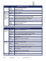
1
M87X SERIES MEASUREMENT SYSTEM Monitoring and Recording IED Manual November 27, 2011 ML0021 Document Revision F © 2011 by Bitronics, LLC TABLE OF CONTENTS FIRMWARE VERSION .....................................................................................................................................vii M87x MANUAL SET .......................................................................................................................................viii INSTALLATION AND MAINTENANCE ............................................................................................................ix WARRANTY AND ASSISTANCE .....................................................................................................................ix AUTHORIZED REPRESENTATIVE IN THE EUROPEAN UNION ................................................................... x COPYRIGHT NOTICE ........................................................................................................................................ x TRADEMARKS .................................................................................................................................................. x SAFETY SECTION ...........................................................................................................................................xii WARNING: EMISSIONS – CLASS A DEVICE (EN55011) ............................................................................xv Decommissioning and Disposal ...................................................................................................................xv 1.0 DESCRIPTION ............................................................................................................................................ 1 1.1 Introduction .............................................................................................................................................. 1 1.2 Features .................................................................................................................................................. 1 1.3 Specifications .......................................................................................................................................... 1 1.4 Standards and Certifications .................................................................................................................10 1.4.1 Revenue Accuracy .........................................................................................................................10 1.4.2 Environment ...................................................................................................................................10 2.0 HOUSING AND BACKPLANE .................................................................................................................13 2.1 2.2 2.3 2.4 2.5 2.6 2.7 Installation .............................................................................................................................................16 Initial Inspection.....................................................................................................................................16 Protective Ground/Earth Connections...................................................................................................16 Instrument Mounting..............................................................................................................................16 Surge Protection....................................................................................................................................16 Cleaning ................................................................................................................................................16 Removal and Installation of Modules ....................................................................................................17 3.0 HOST / ANALOG-DIGITAL SIGNAL PROCESSOR MODULE H11 .......................................................18 3.1 Host board .............................................................................................................................................18 3.1.1 Serial Port/Front Panel Board ........................................................................................................18 3.1.1a Service Port (P1) .....................................................................................................................18 3.1.1b Standard Serial Ports (P2, P3, P4) ..........................................................................................19 3.1.1c Diagnostic Status LED’s (S1, S2, S3, S4) ...............................................................................20 3.1.1d RS485 Connections .................................................................................................................20 3.1.2 Self-Test Modes .............................................................................................................................27 3.1.3 System Clock .................................................................................................................................28 3.2 A10 Analog-Digital Signal Processor Board .........................................................................................28 3.2.1 Calibration ......................................................................................................................................28 3.2.2 Instantaneous Measurement Principles .........................................................................................28 3.2.2a Sampling Rate and System Frequency ...................................................................................28 4.0 MEASUREMENTS ....................................................................................................................................29 4.1 Current (1/4-Cycle Update) ...................................................................................................................29 4.1.1 Neutral and Residual Current (1/4-Cycle Update) .........................................................................29 4.2 Voltage Channels (1/4-Cycle Update)...................................................................................................29 4.3 Power Factor (1-Cycle Update) .............................................................................................................30 ML0021 November 27, 2011 ii Copyright 2011 Bitronics, LLC 4.4 Watts / Volt-Amperes (VAs) / VARs (1-Cycle Update)..........................................................................30 4.4.1 Geometric VA Calculations ............................................................................................................31 4.4.2 Arithmetic VA Calculations .............................................................................................................31 4.4.3 Equivalent VA Calculations ............................................................................................................32 4.5 Energy (1-Cycle Update) .......................................................................................................................32 4.6 Frequency (1-Cycle Update) .................................................................................................................33 4.7 Demand Measurements (1-Second Update) ........................................................................................33 4.7.1 Ampere and Fundamental Ampere Demand .................................................................................34 4.7.2 Volt Demand ..................................................................................................................................34 4.7.3 Power Demands (Total Watts, VARs, and VAs) ............................................................................35 4.7.4 Voltage THD Demand ....................................................................................................................35 4.7.5 Current TDD Demand ....................................................................................................................35 4.7.6 Demand Resets .............................................................................................................................35 4.7.7 Demand Interval .............................................................................................................................35 4.8 Harmonic Measurements (1-Cycle Update) ..........................................................................................36 4.8.1 Voltage Distortion (THD) (1-Cycle Update) ...................................................................................36 4.8.2 Current Distortion (THD and TDD) (1-Cycle Update) ....................................................................36 4.8.3 Fundamental Current (1-Cycle Update) .........................................................................................37 4.8.4 Fundamental Neutral Current (M871 Only) (1-Cycle Update) .......................................................37 4.8.5 Fundamental Voltage (1-Cycle Update) ........................................................................................37 4.8.6 Fundamental Watts / Volt-Amperes (VAs) / VARs (1-Cycle Update) ............................................38 4.8.7 K-Factor (1-Cycle Update) .............................................................................................................38 4.8.8 Displacement Power Factor (1-Cycle Update) ..............................................................................38 4.8.9 Phase Angle (1-Cycle Update) ......................................................................................................38 4.8.10 Resistance, Reactance, Impedance (1-Cycle Update) ................................................................39 4.8.11 Slip Frequency (1-Cycle Update) .................................................................................................39 4.8.12 Individual Phase Harmonic Magnitudes and Phase Angles (1-Cycle Update) ............................39 4.9 Temperature (1-Second Update) ..........................................................................................................39 4.10 Symmetrical Components (1-Cycle Update) .....................................................................................39 4.11 Supply Voltage and Current Unbalance (1-Cycle Update) ................................................................39 4.12 Flicker ..................................................................................................................................................40 4.13 Fault Analysis ......................................................................................................................................40 4.13.1 Line Parameters ...........................................................................................................................40 4.13.2 Peak Current ................................................................................................................................40 4.13.3 Status Indication and Reset .........................................................................................................40 4.13.4 SOELOG Output ..........................................................................................................................41 4.13.5 Protocol Output ............................................................................................................................41 4.14 List of Available Measurements ..........................................................................................................43 5.0 FUNCTIONAL DESCRIPTION ..................................................................................................................46 5.1 Passwords .............................................................................................................................................46 5.2 Configuration .........................................................................................................................................46 5.3 Triggering ..............................................................................................................................................48 5.3.1 Threshold Trigger ...........................................................................................................................48 5.3.1a Trigger Hysteresis....................................................................................................................48 5.3.2 Digital Input Trigger ........................................................................................................................50 5.3.3 Edge and Level Triggers ................................................................................................................50 5.3.4 Manual Trigger ...............................................................................................................................51 5.3.5 Logical Combinations of Triggers ..................................................................................................51 5.3.6 Cross Triggering Multiple 70 Series Units (Inter-triggering) ..........................................................51 5.3.7 Fault Distance Triggers ..................................................................................................................51 5.3.8 Periodic Triggers ............................................................................................................................52 5.4 Recording ..............................................................................................................................................53 5.4.1 Waveform Recorder .......................................................................................................................53 5.4.1a Default Frequency Setting for Waveform Recorder ................................................................55 5.4.1b Indicating Waveform Records with Digital Outputs .................................................................55 5.4.1c Retrieving and Deleting Waveform Recorder Files .................................................................56 5.4.2 Disturbance Recorders ..................................................................................................................56 5.4.2a Indicating Disturbance Records with Digital Outputs ..............................................................57 5.4.2b Retrieving and Deleting Disturbance Recorder Files ..............................................................57 ML0021 November 27, 2011 iii Copyright 2011 Bitronics, LLC 5.4.3 Trend Recorder ..............................................................................................................................58 5.4.3a Retrieving Trend Records ........................................................................................................58 5.4.4 Comtrade Format ...........................................................................................................................58 5.4.4a Comtrade ZIP Files ...................................................................................................................59 5.4.5 IEEE Long File Naming Convention ...............................................................................................59 5.4.6 Voltage Fluctuation Table (VFT) File ..............................................................................................61 5.4.7 Sequence of Events (SOE) File ......................................................................................................63 5.5 M87x File System ..................................................................................................................................63 5.5.1 FTP Server .....................................................................................................................................63 5.5.1a Introduction to FTP ..................................................................................................................63 5.5.1b M87x FTP Implementation ......................................................................................................64 5.5.2 Zmodem, TELNET, and Command Line Interface ........................................................................65 5.6 Assigning Pulse Outputs to Energy Values ..........................................................................................66 5.7 IRIG-B ...................................................................................................................................................66 5.7.1 Overview ........................................................................................................................................66 5.7.2 Introduction to IRIG Standards ......................................................................................................67 5.7.2a Time Code Format (Rate Generation) .....................................................................................67 5.7.2b Format Designation .................................................................................................................67 5.7.2c Carrier/Resolution ....................................................................................................................68 5.7.2d Coded Expressions .................................................................................................................68 5.7.3 M87x IRIG-B Implementation.........................................................................................................68 5.7.3a M87x IRIG-B Receiver .............................................................................................................68 5.7.3b M87x IRIG-B Decoder .............................................................................................................68 5.7.3c M87x IRIG-B Time Qualifier .....................................................................................................69 5.7.4 Determining the Correct Year ........................................................................................................69 5.7.5 Methods of Automatic Clock Adjustments .....................................................................................70 5.7.6 Types of M87x Clock Synchronization ...........................................................................................70 5.7.6a Frequency Adjustments and Free Wheeling ...........................................................................70 5.7.6b Permanent IRIG-B Source Connection ...................................................................................71 5.7.7 Stages of IRIG-B Synchronization and Accuracy ..........................................................................71 5.7.7a Power-Up Stage ......................................................................................................................71 5.7.7b Time Lock Stage ......................................................................................................................71 5.7.7c Frequency Lock Stage .............................................................................................................72 5.7.7d Final Lock Stage ......................................................................................................................72 5.7.8 Notes On Operation .......................................................................................................................72 5.7.9 IRIG-B Electrical Specifications .....................................................................................................72 5.7.10 IRIG-B Port Wiring Instructions (Pulse Width Coded, IRIG-B master, .........................................72 Demodulated)...........................................................................................................................................72 5.7.11 Modulated IRIG-B .........................................................................................................................73 5.7.12 Setup Instructions for Use of the M87x Modulated IRIG-B Converter (Sine ................................73 Wave, Amplitude Modulated, IRIG-B master) ..........................................................................................73 5.8 Time Sync & Setting .............................................................................................................................74 5.8.1 Time Sync Status Registers .........................................................................................................74 5.8.2 Manual time setting by Command-Line instruction .....................................................................74 5.8.3 Unsolicited DNP Time set (DNP master sets the IED clock) ......................................................74 5.8.4 IRIG-B Time sync (time-synchronization via dedicated IED port) ..............................................74 5.8.5 (UCA) Network Time Synchronization - time synchronization over Ethernet .............................75 5.8.6 SNTP (Simple Network Time Protocol) - time synchronization over Ethernet ...........................75 5.8.7 DNP Time sync (slave requesting DNP time be set) ..................................................................75 5.9 Using the M87x with a Bitronics Analog Output Converter ...................................................................76 5.10 Automatic Event Notification ...............................................................................................................76 5.10.1 Email Notifications .......................................................................................................................76 5.10.2 Serial Notifications .......................................................................................................................76 5.10.3 Data Sent .................................................................................................................................76 5.10.4 Error Recovery.........................................................................................................................77 5.10.5 Example ...................................................................................................................................77 5.10.6 Control Characters....................................................................................................................77 6.0 POWER SUPPLY V10 ..............................................................................................................................78 6.1 Introduction ............................................................................................................................................78 ML0021 November 27, 2011 iv Copyright 2011 Bitronics, LLC 6.2 Features ................................................................................................................................................78 6.3 Specifications ........................................................................................................................................78 6.3.1 Environmental ................................................................................................................................79 6.3.2 Physical ..........................................................................................................................................79 6.4 Power Supply and Protective Ground (Earth) Connections ..................................................................80 6.5 Overcurrent Protection ..........................................................................................................................80 6.6 Supply/Mains Disconnect ......................................................................................................................80 7.0 SIGNAL INPUT MODULE S10, S11, S12 (M871) S13, S14, S15, S16, S17 (M872) ..............................81 7.1 Introduction ............................................................................................................................................81 7.2 Features ................................................................................................................................................81 7.3 Specifications ........................................................................................................................................82 7.4 Current Input (CT) Connections ............................................................................................................87 7.5 Voltage Input (VT) Connections ............................................................................................................87 7.6 Current Measurements..........................................................................................................................87 7.6.1 Neutral Current (Residual Current) for WYE Connections ............................................................87 7.7 Voltage Measurements .........................................................................................................................87 7.8 Changing Transformer Ratios ...............................................................................................................88 7.9 User (External Transformer) Gain and Phase Correction .....................................................................88 7.10 Calibration ...........................................................................................................................................88 8.0 ETHERNET MODULE P10, P11, P12 ......................................................................................................97 8.1 Introduction ............................................................................................................................................97 8.2 Features ................................................................................................................................................98 8.3 Specifications ........................................................................................................................................98 8.4 Environmental .......................................................................................................................................99 8.5 Physical .................................................................................................................................................99 8.6 Hot Swap (HS) Compatibility .................................................................................................................99 8.7 Hardware Configuration ........................................................................................................................99 8.8 Cabling ..................................................................................................................................................99 8.9 Connections ........................................................................................................................................100 8.10 Troubleshooting the Connection .......................................................................................................100 8.11 Indicators ...........................................................................................................................................100 8.12 Software Configuration ......................................................................................................................100 8.13 Technical Details ...............................................................................................................................101 8.13.1 Jumper Settings .........................................................................................................................102 8.13.2 Troubleshooting .........................................................................................................................103 8.13.3 PHYSTS Register Contents .......................................................................................................104 8.13.4 Statistics Gathered by Ethernet Driver ......................................................................................105 9.0 DIGITAL INPUT / OUTPUT MODULE P30A, P31 .................................................................................106 9.1 Introduction ..........................................................................................................................................106 9.2 Features ..............................................................................................................................................106 9.3 Specifications ......................................................................................................................................107 9.4 Environmental .....................................................................................................................................108 9.5 Physical ...............................................................................................................................................108 9.6 Hot Swap (HS) Compatibility ...............................................................................................................108 9.7 Description ...........................................................................................................................................108 9.7.1 P30A .............................................................................................................................................108 9.7.2 P31 ...............................................................................................................................................109 9.8 System Design Considerations ...........................................................................................................109 9.8.1 Input / Output Impedance .............................................................................................................109 9.8.2 Input Assignments .......................................................................................................................109 9.9 Debounce Time Setting .......................................................................................................................109 9.10 Setting Digital I/O Module Jumpers...................................................................................................112 9.10.1 Disassembly of the P30A Module ..............................................................................................112 9.10.2 Disassembly of the P31 Module ................................................................................................112 TM 9.10.3 CompactPCI Interface Board (692) Jumper Settings .............................................................113 9.10.4 I/O Board (693) Jumper Settings ...............................................................................................114 9.10.5 Health Status Digital Output Setting (Optional assignment of Digital Output 1 of Module 0) ....116 ML0021 November 27, 2011 v Copyright 2011 Bitronics, LLC 10.0 TRANSDUCER INPUT MODULE P40..................................................................................................117 10.1 Introduction ........................................................................................................................................117 10.2 Features ............................................................................................................................................118 10.3 Specifications ....................................................................................................................................119 10.4 Environmental ...................................................................................................................................119 10.5 Physical .............................................................................................................................................120 10.6 Hot Swap (HS) Compatibility.............................................................................................................120 10.7 Description .........................................................................................................................................120 10.8 System Design Considerations .........................................................................................................120 10.8.1 Input Type Jumper Settings ...........................................................................................................120 10.8.2 Transducer Input Scaling Configuration .........................................................................................122 10.8.3 Setting the Data Update Rate (Poll rate) for P40 Transducer Inputs .............................................122 Appendix A - Cross Triggering ...................................................................................................................124 Appendix B - Firmware Version History .....................................................................................................140 ML0021 November 27, 2011 vi Copyright 2011 Bitronics, LLC FIRMWARE VERSION The following table provides the most recent firmware and software versions. For best results, the Configurator version used should match with the firmware version. A complete list of firmware and software versions is provided on the 70 Series Utilities CD. NOTE: Host firmware version 3.01 requires 70 Series IEDs with 64 MB SDRAM. Do not attempt to upgrade older 70 Series IEDs with insufficient memory to v3.01. Firmware Versions Description M870 Family M87x Product Release, New Hardware supported Dual Bus, Analog I/O M87x Updated Release M87x Updated Release M87x Updated Release M87x Product Release, Fault Location, Adjustable Sample Rate M87x Product Release; Add Demand per phase for Watts ,VAr, & VA. Configurator & Biview improvements w/ modems. Change to Digital I/O default watchdog contact (Configurator setup; not firmware dependent). Support new version of hardware on P3x, P4x modules. M87x Product Release: Added 1mHz accuracy on M87x. Improved poll rate from 500ms to 100ms for a single P40 transducer inputs module (M87x). Fault distance configuration is changed. Time sync with respect to DNP master is changed from the DNP master jamming the time to asking the master what time to jam. Increased waveform recording limit from 999 post trigger for longer recording. Mx7x Product Release, IEC61850 & SNTP; Avg 3-Ph Amps and Avg 3-Ph Volts ML0021 Bios Version DSP Firmware Host Firmware 2.1/3.0* 2.1/3.0* 2.1/3.0* 2.1/3.0* 1.21 " 1.24 1.24 2.05 2.06 2.12 2.15 3.40 1.30 2.17 3.40 1.30 2.18 3.00A 2.57 10/17/08 3.40 1.31 2.19 3.02 2.58 09/30/2009 3.40 1.30 3.01.0 November 27, 2011 vii Utilities CD Release Date 2.31 2.32 2.39 2.41 2.43 2.44 2.50 2.52 03/24/06 04/14/06 10/06/06 12/18/06 2.43 2.56 12/21/07 Configurator 3.01 3.01 1/30/2009 Copyright 2011 Bitronics, LLC Firmware Versions Bios Description Version M87x Product Release: Added 1mHz accuracy on M87x. Improved poll rate from 500ms to 100ms for a single P40 transducer inputs module (M87x). Fault distance configuration is changed. Time sync with respect to DNP master is changed from the DNP master jamming the time to asking the master what time to jam. Increased waveform recording limit from 999 post trigger for longer 3.40 recording. DSP Firmware Host Firmware Configurator Utilities CD 1.31 3.02.0 3.02 3.02 09/30/2009 3.40 1.31 3.04 3.04 3.04 10/15/2010 M87x Product Release: Added support for dual peak current input range M872 (S16, S17), IEEE C37.232 naming convention, periodic triggering, and 4 IEC 61850 buffered reports. 3.40 1.32 3.05 3.05 3.05 2/28/2011 M87x Product Release: Increased pre and post trigger times for DR recorders, modified base memory to 1MB 3.40 1.32 3.07 3.07 3.07 11/11/2011 M87x Product Release: Added virtual I/O to DR. Added Peak Fault Current Measurement. Improved password security. Added support for control characters for SMS. * H10/H11 Release Date M87X MANUAL SET ML0021 ML0022 ML0024 ML0025 ML0026 ML0027 ML0034 ML0021 M87x User Manual 70 SERIES UCA® Manual M87x Modbus Plus Module & Protocol 70 SERIES Modbus Protocol 70 SERIES DNP3 Protocol M870D Remote Display Manual 70 SERIES IEC61850® Protocol Manual November 27, 2011 viii Copyright 2011 Bitronics, LLC CERTIFICATION Bitronics LLC certifies that the calibration of our products is based on measurements using equipment whose calibration is traceable to the United States National Institute of Standards Technology (NIST). INSTALLATION AND MAINTENANCE Bitronics LLC products are designed for ease of installation and maintenance. As with any product of this nature, installation and maintenance can present electrical hazards and should be performed only by properly trained and qualified personnel. If the equipment is used in a manner not specified by Bitronics LLC, the protection provided by the equipment may be impaired. In order to maintain UL recognition, the following Conditions of Acceptability shall apply: a) Terminals and connectors that shall be connected to live voltages are restricted to nonfield wiring applications only. b) After installation, all hazardous live parts shall be protected from contact by personnel or enclosed in a suitable enclosure. WARRANTY AND ASSISTANCE This product is warranted against defects in materials and workmanship for a period of thirty-six (36) months from the date of their original shipment from the factory. Products repaired at the factory are likewise warranted for eighteen (18) months from the date the repaired product is shipped, or for the remainder of the product's original warranty, whichever is greater. Obligation under this warranty is limited to repairing or replacing, at our designated facility, any part or parts that our examination shows to be defective. Warranties only apply to products subject to normal use and service. There are no warranties, obligations, liabilities for consequential damages, or other liabilities on the part of Bitronics LLC except this warranty covering the repair of defective materials. The warranties of merchantability and fitness for a particular purpose are expressly excluded. For assistance, contact Bitronics LLC at: Telephone: Fax: Email: Website: 610.997.5100 610.997.5450 [email protected] www.novatechweb.com/bitronics Shipping: 261 Brodhead Road Bethlehem, PA 18017-8698 USA ML0021 November 27, 2011 ix Copyright 2011 Bitronics, LLC AUTHORIZED REPRESENTATIVE IN THE EUROPEAN UNION NovaTech Europe BVBA Kontichsesteenweg 71 2630 Aartselaar Belgium T +32.3.458.0807 F +32.3.458.1817 E [email protected] COPYRIGHT NOTICE This manual is copyrighted and all rights are reserved. The distribution and sale of this manual is intended for the use of the original purchaser or his agents. This document may not, in whole or part, be copied, photocopied, reproduced, translated or reduced to any electronic medium or machine-readable form without prior consent of Bitronics LLC, except for use by the original purchaser. The product described by this manual contains hardware and software that is protected by copyrights owned by one or more of the following entities: Bitronics LLC, 261 Brodhead Road, Bethlehem, PA 18017; Ardence, Inc., Five Cambridge Center, Cambridge, MA 02142; SISCO, Inc., 6605 19½ Mile Road, Sterling Heights, MI 48314-1408; General Software, Inc., Box 2571, Redmond, WA 98073; Schneider Automation, Inc., One High Street, North Andover, MA 01845; Triangle MicroWorks, Inc., 2213 Middlefield Court, Raleigh, NC 27615 Greenleaf Software Inc., Brandywine Place, Suite 100, 710 East Park Blvd, Plano, TX 75074 TRADEMARKS The following are trademarks or registered trademarks of Bitronics LLC: The Bitronics logo Bitronics PowerPlex Triplex Triple-II MultiComm PowerServe SubCycle Technology SubCycleStuf The following are trademarks or registered trademarks of AREVA T&D Inc. AREVA T&D the AREVA logo MiCOM The following are trademarks or registered trademarks of the DNP User's Group: DNP DNP3 The following are trademarks or registered trademarks of the Electric Power Research Institute (EPRI): UCA. UCA2 The following are trademarks or registered trademarks of Schneider Automation, Inc.: MODSOFT Modicon Modbus Plus Modbus Compact 984 PLC The following are trademarks or registered trademarks of Ardence, Inc.: Phar Lap the Phar Lap logo ML0021 November 27, 2011 x Copyright 2011 Bitronics, LLC The following are trademarks or registered trademarks of Systems Integration Specialists Company, Inc. (SISCO): SISCO MMS-EASE Lite AX-S4MMS The following are trademarks or registered trademarks of General Software, Inc.: General Software the GS logo EMBEDDED BIOS Embedded DOS The following are trademarks or registered trademarks of the PCI Industrial Computer Manufacturers Group: CompactPCI PICMG the CompactPCI logo the PICMG logo ML0021 November 27, 2011 xi Copyright 2011 Bitronics, LLC SAFETY SECTION This Safety Section should be read before commencing any work on the equipment. Health and safety The information in the Safety Section of the product documentation is intended to ensure that products are properly installed and handled in order to maintain them in a safe condition. It is assumed that everyone who will be associated with the equipment will be familiar with the contents of the Safety Section. Explanation of symbols and labels The meaning of symbols and labels that may be used on the equipment or in the product documentation is given below. Installing, Commissioning and Servicing Equipment connections Personnel undertaking installation, commissioning or servicing work on this equipment should be aware of the correct working procedures to ensure safety. The product documentation should be consulted before installing, commissioning or servicing the equipment. Terminals exposed during installation, commissioning and maintenance may present a hazardous voltage unless the equipment is electrically isolated. If there is unlocked access to the equipment, care should be taken by all personnel to avoid electric shock or energy hazards. ML0021 November 27, 2011 xii Copyright 2011 Bitronics, LLC Voltage and current connections should be made using insulated crimp terminations to ensure that terminal block insulation requirements are maintained for safety. To ensure that wires are correctly terminated, the correct crimp terminal and tool for the wire size should be used. Before energizing the equipment, it must be grounded (earthed) using the protective ground (earth) terminal, or the appropriate termination of the supply plug in the case of plug connected equipment. Omitting or disconnecting the equipment ground (earth) may cause a safety hazard. The recommended minimum ground (earth) wire size is 2.5 mm2 (#12 AWG), unless otherwise stated in the technical data section of the product documentation. Before energizing the equipment, the following should be checked: 1. Voltage rating and polarity 2. CT circuit rating and integrity of connections 3. Protective fuse rating 4. Integrity of ground (earth) connection (where applicable) 5. Equipment operating conditions The equipment should be operated within the specified electrical and environmental limits. Current transformer circuits Do not open the secondary circuit of a live CT since the high voltage produced may be lethal to personnel and could damage insulation. Battery replacement Where internal batteries are fitted, they should be replaced with the recommended type and be installed with the correct polarity, to avoid possible damage to the equipment. Internal battery is 3v lithium coin cell, Panasonic BR2330. The battery supplies uninterruptible power to the real-time clock when the device is not powered normally. There are no other loads on the battery but the clock. When the unit is operating, the auxiliary power supply sources the clock, leaving the battery unloaded through the majority of its useable life except for brief intervals when the device is powered down (shipping, storage, etc.) Maximum expected life is dictated by the manufacturer’s advertised shelf life, about 10 years which is typical for Lithium batteries in this class. The minimum expected life is determined by the rated capacity of 255mAh, which can be expected to carry the full load of the clock if the unit remains unpowered for about three years or more. ML0021 November 27, 2011 xiii Copyright 2011 Bitronics, LLC If the auxiliary power to the device should be interrupted after the battery has fully discharged, the time and date settings will initially be lost when the power is restored. However, if the device’s clock is normally synchronized by an external source such as IRIG-B, the correct time and date will be restored by the first IRIG update following the power interruption. There are no other adverse effects resulting from eventual loss of the battery’s charge. There is no automatic provision to indicate the health of the battery. The status can be determined by cycling the power to the device then checking to determine if the clock has lost its time and date settings. Measuring the voltage of the battery, although effective, is not generally considered practical since it also requires powering the device down in order to gain access to the battery, thus providing no advantage over the recommended method. Insulation and dielectric strength testing Insulation testing may leave capacitors charged up to a hazardous voltage. At the end of each part of the test, the voltage should be gradually reduced to zero, to discharge capacitors, before the test leads are disconnected. Removal and insertion of modules All M87x active circuitry is located on removable modules. Unless a Module is specifically intended for Hot Swap (see documentation), it must not be inserted into or withdrawn from equipment while it is energized, since this may result in damage. Hot Swap modules may be installed and removed under power. Refer to the appropriate section or manual to determine if the particular module is Hot Swap compatible. For all other modules, remove all power from the unit before installing or removing any module. All Hazardous Voltages MUST be removed from the M87x before removing or installing the Power Supply Module (Vxx) or the Signal Input Module (S1x). All connections to a module must be removed before removing the module. Do not attempt to install a module with signals connected. Fiber optic communication Where fiber optic communication devices are fitted, these should not be viewed directly. Optical power meters should be used to determine the operation or signal level of the device. ML0021 November 27, 2011 xiv Copyright 2011 Bitronics, LLC WARNING: EMISSIONS – CLASS A DEVICE (EN55011) This is a Class A industrial device. Operation of this device in a residential area may cause harmful interference, which may require the user to take adequate measures. DECOMMISSIONING AND DISPOSAL 1. Decommissioning The auxiliary supply circuit in the equipment may include capacitors across the supply or to ground (earth). To avoid electric shock or energy hazards, after completely isolating the supplies to the relay (both poles of any dc supply), the capacitors should be safely discharged via the external terminals before decommissioning. 2. Disposal It is recommended that incineration and disposal to watercourses is avoided. The product should be disposed of in a safe manner. Any products containing batteries should have them removed before disposal, taking precautions to avoid short circuits. Particular regulations within the country of operation may apply to the disposal of lithium batteries. ML0021 November 27, 2011 xv Copyright 2011 Bitronics, LLC 1.0 DESCRIPTION 1.1 Introduction The M87x family of monitoring and recording IEDs with SubCycleTM technology is a major breakthrough in power measurement technology. The M87x IEDs were designed to expand the limits of range, speed, and accuracy of measurement, speed of communications, and modularity. It combines a modular-by-board chassis featuring a CompactPCITM card cage, with a dual processor measurement system featuring a 32-bit floating point Digital Signal Processor (DSP) and a 486-based host processor. 1.2 Features Extensive measurement set including two sets of voltages and currents with corresponding power and energy on some models Simultaneous support of multiple protocols over multiple physical links Two completely independent Disturbance Recorders Two separate Waveform Recorders Trend Recorder Sequence of Event log Voltage Fluctuation Table to use for sag and swell reporting Two options for analog inputs, 8 voltages with 4 currents and 2 auxiliary voltages or 8 voltages with 6 currents 128 samples per cycle, 16 bit sampling. 32-bit floating point DSP, capable of 180 MFLOPS (Million Floating Point Operations Per Second). A 128-point complex Fast Fourier Transform (FFT) is performed in less than 50 microseconds. 486-class Host processor. Watchdog timer maximizes system reliability. 4 Configurable serial ports - Three RS232/RS485 ports and one DB9M Service RS232 port Fully compatible CompactPCITM backplane and system bus. Rugged all-aluminum housing. Choice of standard chassis (C07A5) with 3 option cPCI expansion bays, intermediate chassis (C10A7) with 5 option bays or extended model (C12A8) with 6 option bays. Option modules include digital I/O (P30A and P31), Ethernet (P10, P11, P12), Modbus Plus (P20) and transducer input (P40) 1.3 Specifications Power Supply Input Voltage Nominal: 24-250Vdc, 69-240Vac (50/60Hz) Operating Range: 20-300Vdc, 55-275Vac (45-65Hz) Burden: 50VA max, 20W max (C07A5) 70VA max, 25W max (C12A8 and C10A7) ML0021 November 27, 2011 1 Copyright 2011 Bitronics, LLC CT Current Inputs (S10) CT Current Inputs (S11) CT Current Inputs (S12) VT (PT) AC Voltage Inputs (S10, S11, S12) Terminals 9 to 16 ML0021 Configuration Nominal Peak Current Overload Isolation Burden Frequency Configuration Nominal Peak Current Overload Isolation Burden Frequency Configuration Nominal Peak Current Overload Isolation Burden Frequency Configuration Nominal System Voltage Peak Voltage Impedance Input Signals (S10, S11, S12) 4 Inputs. 3 Phase Currents and 1 Neutral. 5Aac Linear to 100A symmetrical (141A peak) at all rated temperatures. 30Aac continuous. Withstands 400Aac for 2 seconds. 2500Vac, minimum. 0.04VA @ 5A rms, 60Hz (0.0016Ω @ 60Hz). 15-70Hz 4 Inputs. 3 Phase Currents and 1 Neutral. 1Aac/5Aac Linear to 20A symmetrical (28A peak) at all rated temperatures. 30Aac continuous. Withstands 400Aac for 2 seconds. 2500Vac, minimum. 0.0016VA @ 1A rms, 60Hz (0.0016Ω @ 60Hz). 15-70Hz 4 Inputs. 3 Phase Currents and 1 Neutral. 1Aac Linear to 4A symmetrical (5.7A peak) at all rated temperatures. 30Aac continuous. Withstands 400Aac for 2 seconds. 2500Vac, minimum. 0.0016VA @ 1Arms, 60Hz (0.0016Ω @ 60Hz). 15-70Hz 8 Inputs, Measures 2 Buses, 3 or 4 Wire. 120Vac Intended for use on nominal system voltages up to 480V rms phase-to-phase (277V rms phase-to-neutral). Reads to 600V peak (425V rms), input-to-case (ground) >7.5MΩ, input-to-case (ground) November 27, 2011 2 Copyright 2011 Bitronics, LLC (cont’d) Voltage Withstand Frequency Configuration Nominal System Voltage AUX Measurement Voltage Inputs (S10, S11, S12) Terminals Peak Voltage 17 & 18 Impedance Voltage Withstand Frequency CT Current Inputs (S13) CT Current Inputs (S14) ML0021 Configuration Nominal Peak Current Overload Isolation Burden Frequency Configuration Nominal Peak Current Overload Isolation Burden Frequency Input Signals (S10, S11, S12) 2.5kV rms 1min, input-to-case (ground) 2kV rms 1min, input-to-input 15-70Hz 2 Inputs: VAX1 & VAX2 125Vdc / 120Vac Intended for use on nominal AC system voltages up to 480V rms phase-to-phase (277V rms phase-to-neutral), and DC system voltages up to 250Vdc. Reads to 600V peak (425V rms), input-to-case (ground) >7.5MΩ, input-to-case (ground) 2.5kV rms 1min, input-to-case (ground) 2kV rms 1min, input-to-input DC-70Hz Input Signals (S13, S14, S15, S16, S17) 6 Inputs. 2 sets of 3 Phase Currents 5Aac Linear to 100A symmetrical (141A peak) at all rated temperatures. 30Aac continuous. Withstands 400Aac for 2 seconds. 2500Vac, minimum. 0.04VA @ 5A rms, 60Hz (0.0016Ω @ 60Hz). 15-70Hz 6 Inputs. 2 sets of 3 Phase Currents 1Aac/5Aac Linear to 20A symmetrical (28A peak) at all rated temperatures. 30Aac continuous. Withstands 400Aac for 2 seconds. 2500Vac, minimum. 0.0016VA @ 1A rms, 60Hz (0.0016Ω @ 60Hz). 15-70Hz November 27, 2011 3 Copyright 2011 Bitronics, LLC CT Current Inputs (S15) Configuration Nominal Peak Current Overload Isolation Burden Frequency CT Current Configuration Inputs (S16) Nominal M872 with dual Peak Current peak ranges 20A/100A Overload Isolation Burden Frequency CT Current Configuration Inputs (S17) Nominal M872 with dual Peak Current peak ranges 4A/20A Overload Isolation Burden Configuration VT (PT) AC Configuration Voltage Inputs Nominal (S13, S14, System Voltage S15, S16, S17) Terminals 9 to Peak Voltage 16 Impedance ML0021 Input Signals (S13, S14, S15, S16, S17) 6 Inputs. 2 sets of 3 Phase Currents 1Aac Linear to 4A symmetrical (5.7A peak) at all rated temperatures. 30Aac continuous. Withstands 400Aac for 2 seconds. 2500Vac, minimum. 0.0016VA @ 1Arms, 60Hz (0.0016Ω @ 60Hz). 15-70Hz 6 Inputs. 3 Phase Currents from 2 Lines with different peak current ranges. 5Aac Linear to 20A symmetrical (28A peak)/linear to 100A symmetrical (141A peak) at all rated temperatures. 30Aac continuous. Withstands 400Aac for 2 seconds. 2500Vac, minimum. 0.04VA @ 5A rms, 60Hz (0.0016ohms @ 60Hz). 15-70Hz 6 Inputs. 3 Phase Currents from 2 Lines with different peak current ranges. 1Aac Linear to 4A symmetrical (5.7A peak)/linear to 20A symmetrical (28A peak at all rated temperatures. 30Aac continuous. Withstands 400Aac for 2 seconds. 2500Vac, minimum. 0.04VA @ 5A rms, 60Hz (0.0016ohms @ 60Hz). 6 Inputs. 3 Phase Currents from 2 Lines with different peak current ranges. 8 Inputs, Measures 2 Buses, 3 or 4 Wire. 120Vac Intended for use on nominal system voltages up to 480V rms phase-to-phase (277V rms phase-to-neutral). Reads to 600V peak (425V rms), input-to-case (ground) >7.5MΩ, input-to-case (ground) November 27, 2011 4 Copyright 2011 Bitronics, LLC Voltage Withstand Frequency Sample Rate Data Update Rate Number of Bits Input Signals (S13, S14, S15, S16, S17) 2.5kV rms 1min, input-to-case (ground) 2kV rms 1min, input-to-input 15-70Hz Sampling System 128 samples per cycle Amps, Volts Available every ¼ cycle Watts, VAs, VARs, Available every cycle PF 16 Accuracy Accuracies are specified at nominal Frequency and 25C, unless otherwise specified. Temperature Coefficient <25ppm. All values are true RMS and include Harmonics to the 63rd (minimum) Voltage AC: Better than 0.1% of reading (20 to 425V rms, input-to-case). DC (AUX Inputs): +/- 0.2V (24 to 250Vdc, input-to-case) Current (S10, Better than 0.1% of reading +/- 500μA (0.5A to 100.0A), S13, S16 bus 2) Better than 0.1% of reading +/- 1mA (0.05A to 0.5A). Current (S11, Better than 0.1% of reading +/- 100μA (0.5A to 20.0A), S14, S16 bus 1, Better than 0.1% of reading +/- 250μA (0.05A to 0.5A). S17 bus 2) Current (S12, Better than 0.1% of reading +/- 20μA (0.1A to 4.0A), S15, S17 bus 1) Better than 0.1% of reading +/- 50μA (0.01A to 0.1A). Frequency +/- 0.001 Hertz (accuracy is specified at nominal Frequencies and over operating temperature range) Phase Angle +/- 0.2 Deg Power Better than 0.2% of reading (>20% of nominal inputs, 1PF to 0.7PF) ML0021 November 27, 2011 5 Copyright 2011 Bitronics, LLC Operating Temperature Relative Humidity Installation Category Pollution Degree Enclosure Protection Altitude Intended Use Connections Current (S10, S11, S12) Current (S13, S14, S15, S16, S17) Voltage (CE units) Voltage (non-CE) ML0021 Environmental -40C to 70C 0-95% non-condensing IC III (Distribution Level) Refer to definitions below. Pollution Degree 2 Refer to definitions below. IP20 to IEC60529:1989 Up to and including 2000m above sea level Indoor use; Indoor/Outdoor use when mounted in an appropriately rated protective enclosure to NEMA or IP protection classifications, as required for the installation. Physical Terminal block with 10-32 Studs for current inputs. Accepts #10-16 AWG (5.3-1.3mm2) wire Recommended Torque: 16 In-Lbs, 1.81 N-m Terminal block with 8-32 Screws for current inputs. Accepts #10-22 AWG (5.3-0.33mm2) wire Recommended Torque: 16 In-Lbs, 1.81 N-m Removable Terminal Block, accepts #22-12 AWG (0.35 to 3.3mm2) wire, or terminal lugs up to 0.250" (6.35mm) wide. Standard 0.200" (5.08mm) header socket accepts other standard terminal types. Precautions must be taken to prevent shorting of lugs at the terminal block. A minimum distance of 1/8" (3mm) is recommended between uninsulated lugs to maintain insulation requirements. Recommended Torque: 10 In-Lbs, 1.13 N-m Removable Terminal Block, accepts #22-12 AWG (0.35 to 3.3mm2) wire, or terminal lugs up to 0.325" (8.25mm) wide. Standard 0.200" (5.08mm) header socket accepts other standard terminal types. Precautions must be taken to prevent shorting of lugs at the terminal block. A minimum distance of 1/8" (3mm) is recommended between uninsulated lugs to maintain insulation requirements. Recommended Torque: 10 In-Lbs, 1.13 N-m Class I equipment to IEC61140: 1997 November 27, 2011 6 Copyright 2011 Bitronics, LLC Inputs 0 – 10V Voltage Range 0 – 1mA Current Range 4 – 20mA Current Range Common Mode Input Range Common Mode Error Accuracy Protection Data Update Rate (Poll Rate) Input / Output Capacitance, any Terminal to Case Power Supply Requirements Hot Swap Connections Package ML0021 -P40 Transducer Input Module 8 bi-directional, jumper selectable for voltage or current range. Overload Range: -12.5 V to +12.5 Vdc Resolution: 0.381 mV Input Resistance: 10KΩ Overload Range: -2.5 mA to +2.5 mA Resolution: 0.0763 μA Input Resistance: 500Ω Overload Range: 0 mA to +25 mA Resolution: 0.381 μA Input Resistance: 50Ω +/- 9V, Input to Chassis Vcm DC 0.3% of FS @ 9Vp Common Mode Vcm 50/60Hz 0.1% of FS @ 9Vp Common Mode AC 0.25% of Full Scale Input Input terminals have internal transzorb clamp and 90V spark gap protection. 100ms minimum (single P40 module); 500ms minimum (multiple P40 modules) 470pF 3.3Vdc, 5Vdc, +/-12Vdc (supplied from backplane) Complies with Hot Swap specification PICMG 2.1 R1.0 for Basic Hot Swap (requires Host Processor re-boot) Removable Terminal Blocks, accepts #16-28AWG (1,4-0,09mm) wire. Recommended Torque Rating is 2.2 In-Lbs, 0.25 N-m. Standard 0.150" (3,81mm) header socket accepts other standard terminal types. Solid core wire is recommended, or stranded wire with the use of “bootlace ferrules,” where these are available. CompactPCITM (3U, 4HP) removable module November 27, 2011 7 Copyright 2011 Bitronics, LLC ML0021 November 27, 2011 8 Copyright 2011 Bitronics, LLC Definitions: Installation Category (Overvoltage Category) III: Distribution Level, fixed installation, with smaller transient overvoltages than those at the primary supply level, overhead lines, cable systems, etc. Pollution: Any degree of foreign matter, solid, liquid, or gaseous that can result in a reduction of electric strength or surface resistivity of the insulation. Pollution Degree 2: Only non-conductive pollution occurs except that occasionally a temporary conductivity caused by condensation is to be expected. ML0021 November 27, 2011 9 Copyright 2011 Bitronics, LLC 1.4 Standards and Certifications 1.4.1 Revenue Accuracy The M87x exceeds the accuracy requirements of ANSI C12.20 and IEC 60687. The accuracy class of the instrument to each standard is determined by the selected Signal Input Module. Module S10, S13, S16 bus 2 S11, S14, S16 bus 1, S17 bus 2 Nominal Current 5A S12,S15, S17 bus 1 1A 5A 1A Certification ANSI C12.20, 0.5CA IEC 60687, 0,5S ANSI C12.20, 0.2CA IEC 60687, 0,2S ANSI C12.20 0.5CA IEC 60687, 0,5S ANSI C12.20, 0.2CA IEC 60687, 0,2S The M87x was tested for compliance with the accuracy portions of the standards only. The form factor of the M87x differs from the physical construction of revenue meters specified by the ANSI/IEC standards and no attempt has been made to comply with the standards in whole. Contact customer service for more information. 1.4.2 Environment UL/CSA Recognized, File Number E164178 UL61010-1, 2nd edition (July 12, 2004; CAN/ CSA No. 61010-1-04 (2nd edition, dated July 12, 2004) If applicable, the CE mark must be prominently marked on the case label. European Community Directive on EMC 2004/108/EC, (replaced former directive 89/336/EEC amended by 92/31/EEC, 93/68/EEC, 98/13/EC), and Directive 91/263/EC [TTE/SES]. European Community Directive on Low Voltage 73/23/EEC 2006/95/EC (replaces former Directive 73/23/EEC) Product and Generic Standards The following product and generic standards were used to establish conformity: Low Voltage (Product Safety): EN 61010-1: 2001 EMC: EN 61326-1: 2006, EN60255-26:2006 (supersedes EN 50263: 2000), EN 61000-6-2: 2005, EN 61000-6-4: 2007, (EN 50081-2: 1993, EN 50082-2: 1995 have been superseded). Radiated Emissions Electric Field Strength EN 60255-25: 2000 / EN55011: 2007/ A2: 2007(supersedes EN55011: 1998 / A1: 1999/A2 : 2002) Group 1, Class A Frequency: 30 - 1000 MHz ML0021 November 27, 2011 10 Copyright 2011 Bitronics, LLC AC Powerline Conducted Emissions EN 60255-25:2000 / EN55011: 2007/ A2: 2007(supersedes EN55011: 1998 / A1: 1999/A2 : 2002) Group 1, Class A Frequency: 150 kHz – 30 MHz 1 MHz Burst Disturbance Test IEC60255-22-1: 1988 Class III Amplitude: 2.5 kV Electrostatic Discharge (ESD) EN 61000-4-2: 1995 / A1:1998 / A2: 2001 Discharge voltage: ± 8 KV Air; ± 4 KV Contact (Additionally meets ± 6kv Contact) Immunity to Radiated Electromagnetic Energy (Radio-Frequency) EN61000-4-3:2006 /A1:2008, Class III (Supersedes IEC 61000-4.3: 1995 & EN61000-4-3: 2002 / A1:2002; and ENV 50204: 1996, on Immunity to Radiated Electromagnetic Energy -Digital Radio Telephones 900MHz & 1890MHz). Frequency: 80 – 1000 MHz Amplitude: 10.0 V/m Modulation: 80% AM @ 1kHz Frequency: 1400-2000 MHz Amplitude: 3.0 V/m Modulation: 80% AM @ 1kHz Frequency: 2000-2700 MHz Amplitude: 1.0 V/m Modulation: 80% AM @ 1kHz Electrical Fast Transient / Burst Immunity EN 61000-4-4: 2004 (supersedes IEC61000-4-4: 1995) Amplitude, Input AC Power Ports: Severity Level 4; Amplitude ± 4 kV Amplitude, Signal Ports: Severity Level 3; Amplitude ± 2 kV Current/Voltage Surge Immunity EN 61000-4-5: 2006 (supersedes IEC61000-4-5: 1995, EN610000-4-5: 1995/A1:2001) Installation Class: 3 Open Circuit Voltage: 1.2 / 50 µs Short Circuit Current: 8 /20 µs Amplitude: 2 kV common mode, 1 kV differential mode Immunity to Conducted Disturbances Induced by Radio Frequency Fields EN 61000-4-6: 2007 (supersedes IEC61000-4-6: 1996, EN 61000-4-6: 1996 / A1:2001) Level: 3 Frequency: 150 kHz – 80 MHz Amplitude: 10 VRMS Modulation: 80% AM @ 1kHz AC Supply Voltage Dips and Short Interruptions EN 61000-4-11: 2004 (supersedes IEC61000-4-11: 1994) Duration: 10ms on auxiliary power supply, under normal operating conditions, without deenergizing. Surge Withstand Capability Test For Protective Relays and Relay Systems ANSI/IEEE C37.90.1: 1989 ML0021 November 27, 2011 11 Copyright 2011 Bitronics, LLC Vibration IEC60255-21-1: 1988 Endurance Class: 1 Shock and Bump IEC60255-21-2: 1988 Bump Class: 1 ML0021 November 27, 2011 12 Copyright 2011 Bitronics, LLC 2.0 HOUSING AND BACKPLANE The M87x chassis is a modular-by-board design, with a rugged aluminum housing specifically designed to meet the harsh conditions found in utility and industrial applications. The chassis features a passive backplane, an embedded and fully compatible CompactPCITM (cPCI) bus section and proprietary signal input and analog (DSP) processor sections. All active circuitry is located on removable modules. There are four types of modules: Power Supply, Signal Input, the Host/Analog-Digital Signal Processor, and cPCI expansion modules. See Figure 1 (below) for the locations of the module bays in the standard chassis. Figure 1 - Front View and Module Assignment (C07A5, M871 Only) The power supply bay utilizes a standard cPCI power connector. The signal input bay uses a self-aligning 24-pin header. The Analog-Digital Signal Processor board interfaces to the PCI Bus with a standard cPCI connector, and uses a 24-pin header to connect to the analog signals from the Signal Input Board. The Host Processor and the cPCI expansion bays have standard cPCI connectors. The expansion bays are fully compatible, both electrically and mechanically with cPCI standards. The Backplane board is an eight-layer circuit board, and contains a 5V, 33MHz cPCI bus. The standard bay assignment for the standard chassis (C07A5) used for the M871 is shown above. The M871 and M872 are also available in an intermediate chassis (C10A7) that adds two additional cPCI expansion bays, and an extended chassis, (C12A8) that adds three additional cPCI expansion bays. ML0021 November 27, 2011 13 Copyright 2011 Bitronics, LLC Figure 2 - Mounting and Overall Dimensions (C07A5) ML0021 November 27, 2011 14 Copyright 2011 Bitronics, LLC 13.45" (342) ø 0.25" 2.33" (59) 5.20" (132) 2.33" (59) 0.27" (6.9) 13.00" (330) 0.23" (5.7) Figure 3 - Mounting and Overall Dimensions (C12A8 and C10A7) ML0021 November 27, 2011 15 Copyright 2011 Bitronics, LLC 2.1 Installation WARNING - INSTALLATION AND MAINTENANCE SHOULD ONLY BE PERFORMED BY PROPERLY TRAINED OR QUALIFIED PERSONNEL. 2.2 Initial Inspection Bitronics instruments are carefully checked and "burned in" at the factory before shipment. Damage can occur however, so please check the instrument for shipping damage as it is unpacked. Notify Bitronics LLC immediately if any damage has occurred, and save any damaged shipping containers. 2.3 Protective Ground/Earth Connections There are two chassis ground points that MUST be connected to Earth Ground (refer to Figure 8, pg. 68). The first is the Protective Ground (Earth) terminal (terminal 2) on the Power Supply input. The minimum Protective Ground (Earth) wire size is 2.5 mm2 (#12 AWG). The second is the mounting flange. Bitronics LLC recommends that all grounding be performed in accordance with ANSI/IEEE C57.13.3-1983. 2.4 Instrument Mounting The unit should be mounted with four #10-32 (M4) screws. Make sure that any paint or other coatings on the panel do not prevent electrical contact. The device is intended to be connected to earth ground at the mounting plate. See Section 2.3. 2.5 Surge Protection Surge protection devices are incorporated into the power supply. See Section 2.3 for grounding/earthed recommendations. If the unit is to be powered from a VT, it is recommended that one side of the VT be grounded at the instrument following ANSI/IEEE C57.13.3-1983. See Section 6.5 for fuse recommendations. 2.6 Cleaning Cleaning the exterior of the instrument shall be limited to the wiping of the instrument using a soft damp cloth applicator with cleaning agents that are not alcohol based, and are nonflammable and non-explosive. ML0021 November 27, 2011 16 Copyright 2011 Bitronics, LLC 2.7 Removal and Installation of Modules All active circuitry is located on removable modules. Hot Swap modules may be installed and removed under power. Refer to the appropriate section or manual to determine if the particular module is Hot Swap compatible. For all other modules, remove all power from the unit before installing or removing any module. All Hazardous Voltages MUST be removed from the M87x before removing or installing the Power Supply Module or the Signal Input Module. The Signal Input Module and the Power Supply may be withdrawn from the housing after removal of the front panel screws. All connections to a module must be removed before removing the module. Do not attempt to install a module with signals connected. To remove a cPCI module, use the following procedure: 1. 2. 3. 4. 5. 6. Remove power from the unit (except Hot Swap modules). Unscrew the M2.5 Phillips front panel screws (note that these are captive screws). The screw in the handle has been left out intentionally. Pull the red sliding release tab up and outward until handle is unlocked. Push the handle downward (when viewed from the front) to lever out the module. Once the module is disengaged from the backplane connector, carefully withdraw the module. Be extremely careful when handling the module, especially the backplane connector. To insert a cPCI module, use the following procedure: 1. 2. 3. 4. Make sure the red sliding release tab is fully extended from the handle, and that the handle is in the downward position (when viewed from the front). Line up the module with the card guides in the appropriate position (the Host/Analog-Digital Signal Processor Module MUST be inserted in the right most double width bay). Use the handle to lever the module into the housing. When the module is fully engaged, tighten the M2.5 Phillips front panel screws. The screw in the handle has been left out intentionally. ML0021 November 27, 2011 17 Copyright 2011 Bitronics, LLC 3.0 HOST / ANALOG-DIGITAL SIGNAL PROCESSOR MODULE H11 The Host/Analog-Digital Signal Processor Module is an assembly consisting of two sections: the Host board and the Analog-Digital Signal Processor board. 3.1 Host board The Host CPU module consists of a 486-class microprocessor, 64 Mbytes of DRAM, 8 Mbytes of non-volatile FLASH memory, an internal PC-AT style ISA bus and peripheral set, four communications ports and a CompactPCITM master bridge. The H11 host module offers non-volatile memory expansion via an optional Compact Flash card. 3.1.1 Serial Port/Front Panel Board The Serial Port/Front Panel Board consists of the four serial driver connectors, four status LED’s, four bi-color serial port LED’s, and a reset button. Port P1 is a PC-AT style 9-pin D connector for the dedicated RS-232 port, and ports P2, P3, and P4 are universal 150-mil, 6-pin removable connectors for the RS-232/RS-485 serial ports. P2, P3, and P4 are software (user) configurable for RS-232 or RS-485 mode. The RS-232 drivers support full and half duplex modes. See Figures 3-6 (pg. 20 -24) for signal assignments. 3.1.1a Service Port (P1) When connecting to the Service port DB9M (P1) from a PC, a null modem cable is required. The Service Port can be used with a PC running a terminal emulation program. Upon startup, the M87x default configuration sets P1 for 9600 baud, 8 data bits, no parity, 1 stop bit and no flow control handshaking. These parameters are user-configurable. A small number of messages are sent to P1 and the M87x then outputs system messages. Enter the command mode by pressing the ENTER key until the system outputs a prompting message. Allowable commands are: Service Port\Zmodem Commands c: dir receive time cd exit reset type chp1 getlog router trigger dr1 chp2 Goose* send trigger dr2 d: ip serial trigger wv1 date mac setlog trigger wv2 del nsap subnet ver dio point password software whoami display on pulse receive vio point display off reboot status Note: * This command is for UCA Goose only and is now referred to as GSSE. Type “help <command>” to find out more about a particular command. commonly used commands are: The more ip - Set Internet Protocol (IP) address information in "dotted decimal" format. The IP ML0021 November 27, 2011 18 Copyright 2011 Bitronics, LLC address defaults to "192.168.0.254". subnet – Set the Subnet mask. The Subnet mask defaults to "255.255.255.0". router – Set the Gateway (Router) address. The Gateway (Router) address defaults to "192.168.0.1". nsap - Set the OSI network address (NSAP) in "space delimited octet string" format. The default address is "49 00 01 42 49 09 01 01" which is a local address not attached to the global OSI network. The correct value for your network should be obtained from the network administrator. The default values are valid for a device that is attached to a local intranet with optional access via a router (such as a device within a substation). time - Set the time as 24-hour UTC time. Time is entered as HH:MM:SS. The factory default is set to GMT. date – Set the date. Date is entered as MM/DD/YYYY. serial - Display M87x serial number exit - Exit command line mode and return to logging mode. If no commands are received for five minutes the device will revert to logging mode. 3.1.1b Standard Serial Ports (P2, P3, P4) These ports can be set to RS-232 or RS-485, and support baud rates up to 115200. Setup of the Serial Ports can be accomplished by using the 70 Series Configurator. The default configuration for the serial ports is: Serial Port Default Settings Port Protocol Parity Baud IED Address Physical Media P1 Zmodem/Display/Log None 9600 P2 DNP 3.0 None 9600 1 RS-232 P3 Modbus Even 9600 1 RS-232 P4 Zmodem/Display/Log None 9600 RS-232 RS-232 The configuration of these ports is stored internally in the "COMM.INI" file (Section 5.2). If, for any reason, the configuration of the serial ports is erroneously set, the factory default settings can be restored by using FTP. The file "COMM.INI" can be deleted, which will return all ports to the factory default setting. The settings can then be changed by using the 70 Series Configurator. Host cable requirements for CE compliance: On ports P2, P3, and P4, as well as a port that utilizes the externally mounted M87x Modulated IRIG-B Converter, install snap-on ferrite (Fair-Rite #0461164181 or equivalent) onto each cable by wrapping the cable through the ferrite opening two ML0021 November 27, 2011 19 Copyright 2011 Bitronics, LLC times before snapping the ferrite closed. Tie RS-485 cable shields (pin 5) to earth ground at one point in system. The recommended torque rating for the terminal block wire fasteners on ports P2-P4 is 2.2 In-Lbs, 0.25 N-m. 3.1.1c Diagnostic Status LED’s (S1, S2, S3, S4) There are four LED’s on the front panel: S1, S2, S3, and S4. They perform the following functions: LED S1 Description On while flash memory is being written to, otherwise off. S2 Flashes every 5 power-line cycles, indicates DSP operating properly. S3 On while CPU is busy. Intensity indicates CPU utilization level. S4 On during internal self-diagnostics after boot-up. 3.1.1d RS485 Connections Note that various protocols and services have different port connection requirements. When making connections to serial ports for Modbus or DNP3 over RS485, 2-wire half duplex is required. This is because it is necessary to maintain a minimum time period (3 1/3 characters) from the time the transmitter shuts off to the next message on the bus in order to guarantee reliable communications. However, when using Zmodem or connecting to the remote display, asynchronous 2 way communications are required, and therefore a 4-wire full duplex (technically RS422) connection is needed. See figure 6 below for RS485 cable wiring diagrams showing both 2 and 4 wire. There are special considerations for multi-drop Zmodem connections. Zmodem protocol was developed for RS232 point-to-point connections so it does not support any standard convention for addressing. Therefore, it does not facilitate multi-drop communications buses. In order to make it possible to use one modem to establish remote communications with multiple 70 Series devices when the Ethernet option (preferred) is not fitted, the following proprietary convention is employed. When using HyperTerminal or a dial-up modem with RS485, the port on the IED must be configured for "Zmodem" protocol, not for "Zmodem/Display/Log". This is done with the pull-down menu in the Configurator program, see illustration below. Selecting Zmodem also enables an address to be set for the selected COM port. When daisy-chaining multiple devices on RS485, each device must have a unique address. ML0021 November 27, 2011 20 Copyright 2011 Bitronics, LLC Type the command "connect 01" (use the actual address assigned) to establish communications with the device in Zmodem protocol using RS485. This command will not be echoed back as you type it. After striking the enter key, the device will return a command prompt (for example c:\>, e:\data>, c:\config>, etc.) Once communications are established, you can now use the command-line interface, exactly as you would with a direct RS232 connection, to control the device (services supported by Zmodem protocol include: download recording files, control digital outputs, reset demands, set time and date, etc.). In order to disconnect from one device and connect to another on the same bus, type the command "exit" to end the session then type “connect 02” (or whatever address you want to connect to). ML0021 November 27, 2011 21 Copyright 2011 Bitronics, LLC Figure 3 - Typical RS-232 & IRIG-B Cable Wiring ML0021 November 27, 2011 22 Copyright 2011 Bitronics, LLC Figure 4 - Typical RS-485 Cable Wiring ML0021 November 27, 2011 23 Copyright 2011 Bitronics, LLC Figure 4 - Typical RS-485 Cable Wiring ML0021 November 27, 2011 24 Copyright 2011 Bitronics, LLC Figure 5 – M870D RS-232 Cable Wiring ML0021 November 27, 2011 25 Copyright 2011 Bitronics, LLC Figure 6 - Host Port Signal Assignment ML0021 November 27, 2011 26 Copyright 2011 Bitronics, LLC 3.1.2 Self-Test Modes The M87x has several self-tests built in to assure that the instrument is performing accurately. Refer to the appropriate protocol manual for details on how to retrieve the self-test information. The following table lists possible faults that would be detected by the self-tests, how the fault is indicated, the effects of the fault and any necessary corrective actions. Bit # Description Self-Test Bits Hardware Effect Default Value 0(LSB) Factory gain calibration of Analog-Digital Signal Processor Module checksum error. A10 EEProm Unit will continue to function using default values, at reduced accuracy. A/D Gain = 1 1 Factory offset calibration of Analog-Digital Signal Processor Module checksum error. A10 EEProm Unit will continue to function using default values, at reduced accuracy. A/D Offset = 0 2 Factory gain calibration of Signal Input Module checksum error. S1x EEProm Unit will continue to function using default values, at reduced accuracy. CT/VT Gain = 1 3 Factory offset calibration of Signal Input Module checksum error. S1x EEProm Unit will continue to function using default values, at reduced accuracy. CT/VT Offset = 0 4 Factory phase calibration of Signal Input Module checksum error. S1x EEProm Unit will continue to function using default values, at reduced accuracy. CT/VT Phase = 0 5 Factory defined internal ratios of Signal Input Module checksum error. (Type of Signal Input Module) S1x EEProm Unit will continue to function. Assumes -S10 Signal Input Module Volts Ratio = 60 :1 Amps Ratio = 14.136 :1 6 User defined external transformer ratio checksum error. S1x EEProm Unit will continue to function using default values (i.e. w/o user ratios). User CT = 5:5, VT = 1:1 7 User gain correction values checksum error. S1x EEProm Unit will continue to function using default values (i.e. w/o user gain). User Gain = 1 8 User phase correction values checksum error. S1x EEProm Unit will continue to function using default values (i.e. w/o user phase). User Phase = 0 9 Factory defined board ID for Analog-Digital Signal Processor Module checksum error. A10 EEProm 10 Factory defined board ID for Signal Input Module checksum error. S1x EEProm 11 User defined denominators for TDD measurement checksum error. S1x EEProm Assumes default TDD Denominator. 12 13 14 DSP program integrity checksum error. DSP stack overflow. Invalid or missing Amp and/or Voltage Scale Factor. A1x DSP Ram A1x DSP Ram H1x Flash File Host trips watchdog, unit reboots. 15 Protocol configuration invalid. H1x Flash File ML0021 November 27, 2011 27 Assumes default Analog-Digital Signal Processor Module. Assumes default Signal Input Module. Host trips watchdog, unit reboots. Protocol will use default Scale Factor M87x uses default protocol configuration Copyright 2011 Bitronics, LLC Module A10 Module -S10 TDD Denom = 5A Secondary Scale Factor = 1:1 M87x register set 3.1.3 System Clock The M87x has an internal System Clock with a lithium battery for backup when no power is applied to the unit. The clock and battery are located on the Host board. The time settings may be changed via the Serial Port (P1) or various communication protocols. Refer to Section 3.1.1a and the appropriate protocol manuals for details. 3.2 A10 Analog-Digital Signal Processor Board The Analog/DSP board is part of the modular M87x system. This board contains amplifiers, track and hold circuits, multiplexers, an analog to digital converter, a digital signal processor (DSP), and a PCI bridge. Analog signals from the CT/VT board are routed through the backplane to the Analog/DSP board. Once on the board each signal is connected to the track and hold circuitry. The track and hold circuitry is designed to hold the channel’s present value during the time required for the analog to digital converter to sample all of the channels. This effectively allows the M87x to simultaneously sample all of its input channels, eliminating any channel-to-channel skew. A single 16-bit analog to digital converter is used for all measurements. The DSP uses the samples to calculate all of the measured parameters. Each sample is corrected for offset and gain using factory calibration values stored in non-volatile memory on the board. Additionally, a continuous DC removal is performed on all inputs, except the AUX Voltages. An adaptive sampling system is used to maintain 128 samples per cycle over the input frequency range of 15 to 70 Hz. See Section 3.2.2. 3.2.1 Calibration Routine re-calibration is not recommended or required. A field calibration check every few years is a good assurance of proper operation. 3.2.2 Instantaneous Measurement Principles The M87x measures all signals at 128 samples/cycle, accommodating fundamental signal frequencies from 15 to 70 Hz. Samples of all bus signals are taken at the same instant in time, using a 16-Bit A/D converter, effectively creating 128 "snapshots" of the system voltage and current per cycle. 3.2.2a Sampling Rate and System Frequency The sampling rate is synchronized to the frequency of any of the bus voltage or current inputs, prioritized as follows: V1A-N, V1B-N, V1C-N, V2A-N, V2B-N, V2C-N, IA, IB, IC. This is the frequency reported as the "System Frequency". The AUX voltage inputs and Neutrals are not used to synchronize the sampling. The sampling rate is the same for all channels. The default system frequency may be set in the Configurator to either 50 or 60 Hz. This will have no effect on the frequency that is reported, or the sample rate when signals are present. It is used to set the default sample rate when the unit cannot detect any applied signal. ML0021 November 27, 2011 28 Copyright 2011 Bitronics, LLC 4.0 MEASUREMENTS Basic measurement quantities are calculated and updated every 1/4 cycle. These quantities include RMS Amperes and RMS Volts. Watts, VARs, VAs, Power Factor, all harmonic-based measurements (such as fundamental-only quantities), Energy, Frequency, and Phase Angle are updated every cycle. Note: For all of the following measurements, it is important to keep in mind that the specific protocol used to access the data may affect the data that is available, or the format of that data. No attempt is made here to describe the method of accessing measurements - always check the appropriate protocol manual for details. 4.1 Current (1/4-Cycle Update) The current signals are transformer coupled, providing a true differential current signal. Additionally, a continuous DC removal is performed on all current inputs. Instrument transformer ratios can be entered for each current input, as described in the Signal Input Module section (Section 7). This can be accomplished via a network and protocol (refer to the specific protocol manual for details) or by using the 70 Series Configurator. When used on 2-element systems, if there are only 2 currents available to measure, a "0" can be written to the CT Ratio for the missing phase current. This will cause the M87x to fabricate the missing phase current from the sum of the other 2 phase currents. This feature is not recommended for WYE connected systems. The average of the 3 current phases ((Ia + Ib + Ic)/3) is also available. The Average 3phase Amps for bus 1 and bus 2 (M872) are calculated and made available on a per cycle basis. 4.1.1 Neutral and Residual Current (1/4-Cycle Update) M871 Signal Input Modules have a separate input for neutral current. This channel is measured just like any of the other current channels, and the result presented as Neutral Current. Additionally, all M87x units calculate the vector sum of the three phase currents, which is known as the Residual Current. The Residual Current is equivalent to routing the common current return wire through the neutral current input on systems without separate current returns for each phase, with the exception that individual Harmonics are not measured on Residual Current. On systems without a Neutral CT, the Residual Current measurement can be used as a substitute for Neutral Current. This allows the Neutral Current input on the M871 to be used to measure any extra currents in the system. 4.2 Voltage Channels (1/4-Cycle Update) The M87x uses a unique voltage connection method, which is combined with simultaneous sampling to provide an extremely flexible voltage measurement system. All voltage inputs are measured relative to a common reference level (essentially panel ground). See Figure 9 (pg. 78-85) and Section 7 for input connection information. Because all phase signals ML0021 November 27, 2011 29 Copyright 2011 Bitronics, LLC are sampled simultaneously (including currents), these signals can be easily combined to form true Phase-to-Phase and Phase-to-Neutral differential measurements with extremely low amplitude and phase errors. It also allows accurate calculation of Bus-to-Bus differential voltages and angles. Each sample is corrected for offset and gain using factory calibration values stored in non-volatile memory on the board. Additionally, a continuous DC removal is performed on all inputs, except the AUX Voltages. The M87x calculates voltages in PRIMARY units, based on the VT Ratios entered. There are separate VT Ratios for each input. Ratios can be entered via a network and protocol (refer to the specific protocol manual for details) or by running the M87x Configurator. The advantages of this method of voltage measurement are apparent when the M87x is used on the common 2, 2-1/2, and 3 element systems (refer to Section 4.4). The M87x is always calculating Line-to-Neutral, Line-to-Line, and Bus-to-Bus voltages with equal accuracy. On 2 element connections, any phase can serve as the reference phase. Further, the M87x can accommodate WYE connections on one Bus, and DELTA connections on the other Bus. On 2-1/2 element systems, one of the phase-to-neutral voltages is missing, and the M87x must create it from the vector sum of the other two phase-to-neutral voltages. In order to configure the M87x for 2-1/2 element mode and which phase voltage is missing, a "0" is written to the phase-to-neutral VT Ratio for the missing phase voltage. The AUX Voltage input measurements (M871 only) are similar to the phase voltages except they do not have continuous DC removal. Both input-to-ground and input-to-input differential voltages are measured. Because they do not have continuous DC removal, they can be used to measure either AC or DC signals, making these measurements useful for Substation battery monitoring, generator field voltages, local bus voltage measurements, etc. The average of the 3 voltage phases ((Va + Vb + Vc)/3) is also available. The Average 3phase Volts for bus 1 and bus 2 are calculated and made available on a per cycle basis. 4.3 Power Factor (1-Cycle Update) The per-phase Power Factor measurement is calculated using the "Power Triangle,” or the per-phase WATTS divided by the per-phase VAs. The Total PF is similar, but uses the Total WATTS and Total VAs instead. The sign convention for Power Factor is shown in Figure 7 (pg. 31). Note that the Total PF calculation depends on the Total VA calculation type chosen (Section 4.4). 4.4 Watts / Volt-Amperes (VAs) / VARs (1-Cycle Update) On any power connection type (2, 2-1/2, and 3 element), the M87x calculates per-element Watts by multiplying the voltage and current samples of that element together. This represents the dot product of the voltage and current vectors, or the true Watts. The perelement VAs are calculated from the product of the per-element Volts and Amps. The perelement VARs are calculated from fundamental VARs. ML0021 November 27, 2011 30 Copyright 2011 Bitronics, LLC In any connection type, the Total Watts and Total VARs is the arithmetic sum of the perelement Watts and VARs. The sign conventions are shown in Figure 7 (pg. 31). When used on 2-element systems, the reference phase voltage (typically phase B) input, is connected to the Neutral voltage input, and effectively causes one of the elements to be zero. See Figure 9 (pg. 78-85) and Section 7 for input connection information. It is not required to use any particular voltage phase as the reference on 2-element systems. When used on 2-element systems the per-element Watts, VARs, and VAs have no direct physical meaning, as they would on 2-1/2 and 3 element systems where they represent the per-phase Watts, VARs, and VAs. When used on 2-1/2 element systems, one of the phase-to-neutral voltages is fabricated, as described in Section 4.2. In all other respects, the 2-1/2 element connection is identical to the 3 element connection. The M87x may be configured to calculate Total VAs in one of several different ways. The calculation method may be selected either by sending a command to the M87x via a network and protocol (refer to the specific protocol manual for details) or by using the 70 Series Configurator. The three methods, Arithmetic, Geometric, and Equivalent (both for WYE and DELTA), all yield the same results when used on balanced systems with no harmonics present. The differences are illustrated below: 4.4.1 Geometric VA Calculations GEOMETRIC = VATOTAL 2 WattsTOTAL + VARsTOTAL 2 This is the traditional definition of Total VAs for WYE or DELTA systems, and is the default method for Total VAs calculation. The value of Total VAs calculated using this method does not change on systems with amplitude imbalance, relative to a balanced system. There is also a relationship to the Total Power Factor which is described in Section 4.3. Total Power Factor calculations using the Geometric VA method will still indicate a "1" on a system with phase amplitude imbalance, or canceling leading and lagging loads. For example, on a system with a lagging load on one phase and an equal leading load on another phase, the Geometric VA result will be reduced relative to a balanced system but the Total Power Factor will still be "1". 4.4.2 Arithmetic VA Calculations ARITHMETIC VATOTAL= (VA− N × I A ) + (VB − N × I B ) + (VC − N × I C ) The Arithmetic VA calculation is not applicable to DELTA connected systems. The value of Total VAs calculated using this method also does not change on systems with amplitude imbalance, relative to a balanced system. The value of Arithmetic VAs will not change on a system with canceling leading and lagging loads. ML0021 November 27, 2011 31 Copyright 2011 Bitronics, LLC There is also a relationship to the Total Power Factor, which is described in Section 4.3. Total Power Factor calculations using the Arithmetic VA method will still indicate a "1" on a system with phase amplitude imbalance, but not with canceling leading and lagging loads. For example, on a system with a lagging load on one phase and an equal leading load on another phase, the value of the Arithmetic VAs will not change relative to a balanced system, but the Total Power Factor will be less than "1". The Total Power Factor calculated with Arithmetic VAs will "see" the reactive elements in this system, while the Total Power Factor calculated with Geometric VAs will not. 4.4.3 Equivalent VA Calculations EQUIVALENT WYE VATOTAL = VA2− N + VB2− N + VC2− N × I A2 + I B2 + I C2 EQUIVALENT DELTA VATOTAL = VA2− B + VB2−C + VC2− A × I A2 + I B2 + I C2 3 The Equivalent VA calculation has not been as commonly used as other approaches, but has been discussed extensively in technical papers. It is also referred to as "System Apparent Power". This approach to the VA calculation may yield results which are surprising to those used to more traditional methods. A system with amplitude imbalance will yield a greater value of Equivalent VAs than a balanced system. There is also a relationship to the Total Power Factor, which is described in Section 4.3. Essentially, Total Power Factor calculations using the Equivalent VA method will not indicate a "1" on any system unless the loads are purely resistive, and the amplitudes are balanced. Further, the Equivalent VA method may yield better results in the presence of harmonics, where Total Power Factor will also be reduced from "1". Refer to industry standards for more information. 4.5 Energy (1-Cycle Update) Separate values are maintained for both positive and negative Watt-hours, positive and negative VAR-hours, and VA-hours, (for each feeder in the M872). These energy quantities are calculated every cycle from the Total Watts, Total VARs, and Total VAs, and the values are stored into non-volatile memory every 15 seconds. Energy values may be reset. All values are reset simultaneously. Refer to the appropriate protocol manual for details. ML0021 November 27, 2011 32 Copyright 2011 Bitronics, LLC 4.6 Frequency (1-Cycle Update) Frequency is calculated every cycle for every input but the Auxiliary Voltages. The M87x monitors the change in Phase Angle per unit time using the Phase Angle measurement for the fundamental generated by the FFT. The System Frequency is the frequency of the input used for synchronizing the sampling rate (Section 3.2.2). Figure 7 - Sign Conventions for Power Measurements 4.7 Demand Measurements (1-Second Update) The traditional thermal demand meter displays a value that represents the logarithmic response of a heating element in the instrument driven by the applied signal. The most positive value since the last instrument reset is known as the maximum demand (or peak demand) and the lowest value since the last instrument reset is known as the minimum demand. Since thermal demand is a heating and cooling phenomenon, the demand value has a response time T, defined as the time for the demand function to change 90% of the difference between the applied signal and the initial demand value. For utility applications, ML0021 November 27, 2011 33 Copyright 2011 Bitronics, LLC the traditional value of T is 15 minutes, although the M87x can accommodate other demand intervals (Section 4.7.7). The M87x generates a demand value using modern microprocessor technology in place of heating and cooling circuits, it is therefore much more accurate and repeatable over a wide range of input values. In operation, the M87x continuously samples the basic measured quantities, and digitally integrates the samples with a time constant T to obtain the demand value. The calculated demand value is continuously checked against the previous maximum and minimum demand values. This process continues indefinitely, until the demand is reset or until the meter is reset (or power removed and reapplied). The demand reset and power-up algorithms are different for each measurement. These routines are further described in following paragraphs. The maximum and minimum demand values are stored in non-volatile memory on the Host Processor module. NOTE: Changing VT or CT ratios does NOT reset demand measurements to zero. Demand Quantity Amperes (1 & 2) Fundamental Amperes Volts (Bus 1 & 2) Total Watts (1 & 2) Total VARs (1 & 2) Total VAs (1 & 2) THD Volts (Bus 1 & 2) TDD Amperes (1 & 2) Phase Reference Phase, Neutral, Residual Phase, Neutral, Residual Phase - Neutral, Phase - Phase Phase - Neutral, Phase - Phase Phase, Neutral, Residual Function Present, Max Present, Max Present, Max, Min Present, Max, Min Present, Max, Min Present, Max, Min Present, Max Present, Max 4.7.1 Ampere and Fundamental Ampere Demand Present Ampere Demands are calculated via the instantaneous measurement data used to calculate the per-phase Amperes. Upon power-up, all Present Ampere Demands are reset to zero. Maximum Ampere Demands are initialized to the maximum values recalled from non-volatile memory. Upon Ampere Demand Reset, all per-phase Present and Maximum Ampere Demands are set to zero. When Ampere Demands are reset, Fundamental Current Demands are also reset. 4.7.2 Volt Demand Present Volt Demands are calculated via the instantaneous measurement data used to calculate the per-phase Volts. Upon power-up all Present Volt Demands are reset to zero. The Maximum Volt Demands and Minimum Volt Demands are initialized to the minimum and maximum values recalled from non-volatile memory. In order to prevent the recording of false minimums a new Minimum Volt Demand will not be stored unless two criteria are met. First, the instantaneous voltage for that particular phase must be greater than 20Vrms (secondary). Second, the Present Demand for that particular phase must have dipped (Present Demand value must be less then previous Present Demand value). Upon Voltage Demand Reset, all per-phase Maximum Voltage Demands are set to zero. Minimum Voltage Demands are set to full-scale. ML0021 November 27, 2011 34 Copyright 2011 Bitronics, LLC 4.7.3 Power Demands (Total Watts, VARs, and VAs) Present Total Watt, VAR, and VA Demands are calculated via the instantaneous measurement data. The Total VA Demand calculation type is based on the instantaneous Total VA calculation type (Section 4.4) Upon power-up, all Present Total Watt, VAR, and VA Demands are reset to the average of the stored Maximum and Minimum values. The Maximum and Minimum Demands are initialized to the minimum and maximum values recalled from non-volatile memory. Upon a demand reset, the Maximum and Minimum Demands are set equal to the Present Total Watt, VAR, and VA Demand values. A demand reset does not change the value of the Present Total Watt, VAR, and VA Demands. 4.7.4 Voltage THD Demand Present Voltage THD Demands are calculated via the instantaneous measurement data used to calculate the per-phase and phase-to-phase Voltage THDs (Section 4.8.1). Voltage THDs are calculated for both Bus 1 and Bus 2. By applying a thermal demand to the THD measurement, the M87x provides a more effective method of determining the severity of a harmonic problem. Upon power-up, all Present Voltage THD Demands are reset to zero. Maximum Voltage THD Demands are initialized to the maximum values recalled from non-volatile memory. Upon Harmonic Demand Reset, all per-phase Present and Maximum Voltage THD demands are set to zero. 4.7.5 Current TDD Demand Present Current TDD Demands are calculated via the instantaneous measurement data. By applying a thermal demand to the TDD measurement, the M87x provides a more effective method of determining the severity of a harmonic problem. Upon power-up, all Present Current TDD Demands are reset to zero. Maximum Current TDD Demands are initialized to the maximum values recalled from non-volatile memory. Upon Harmonic Demand Reset, all per-phase Present and Maximum Current TDD demands are set to zero. 4.7.6 Demand Resets The demand values are reset in four groups: current, voltage, power, and harmonics. This can be accomplished via a network and protocol (refer to the specific protocol manual for details). 4.7.7 Demand Interval The M87x uses 15 minutes as the default demand interval, however it can be changed. Four separate, independent demand intervals may be set for current, voltage, power, and harmonics. The range of demand intervals is 5 to 3600 seconds (1hr). This can be accomplished via a network and protocol (refer to the specific protocol manual for details) or by using the 70 Series Configurator. While the Demand Interval is stored internally as a ML0021 November 27, 2011 35 Copyright 2011 Bitronics, LLC 32-bit number, some protocols may place further restrictions on the Demand Interval due to limitations on numerical format. Please refer to the appropriate protocol manual for details. 4.8 Harmonic Measurements (1-Cycle Update) M87x instruments continually sample all inputs at 128 samples per cycle, and compute a 128-point Fast Fourier Transform (FFT) every cycle for each input. When combined with high dynamic-range input of up to 140APEAK and 600VPEAK, this allows the M87x to make extremely accurate measurements of harmonics, regardless of crest factor. All harmonic and harmonic-based values are calculated every cycle. Both magnitude and phase of each harmonic are provided. In the following sections, Harmonic 0 indicates DC, Harmonic 1 indicates the fundamental, and Harmonic N is the nth multiple of the fundamental. 4.8.1 Voltage Distortion (THD) (1-Cycle Update) Voltage Harmonic Distortion is measured by phase in several 63 different ways. The equation for Total Harmonic Distortion V h2 ∑ h= 2 (THD) is given in Equation 1. For Odd Harmonic Distortion, = × 100% %THD the summation only uses harmonics where h is odd. For Even V1 Harmonic Distortion, the summation only uses harmonics where h is even. Note the denominator is the fundamental magnitude. For Individual Harmonic Distortion there is no Equation 1- Voltage THD summation, only one component is used in the numerator. 4.8.2 Current Distortion (THD and TDD) (1-Cycle Update) Current Harmonic Distortion is measured by phase in several 63 different ways. The first method is Total Harmonic Distortion I h2 ∑ h= 2 (THD). The equation for THD is given in Equation 2. For Odd % THD = × 100% Harmonic Distortion, the summation only uses harmonics I1 where h is odd. For Even Harmonic Distortion, the summation only uses harmonics where h is even. Note the denominator is the Equation 2 - Current fundamental magnitude. Alternatively, Current Harmonic Distortion can be measured 63 as Demand Distortion, as defined by IEEE-519/519A. I h2 ∑ h =2 Demand Distortion differs from traditional Harmonic Distortion % TDD = × 100% IL in that the denominator of the distortion equation is a fixed value. This fixed denominator value is defined as the average monthly peak demand. By creating a measurement that is based on a fixed value, TDD is a "better" measure of distortion Equation 3 - Current problems. Traditional THD is determined on the ratio of harmonics to the fundamental. While this is acceptable for voltage measurements, where the fundamental only varies slightly, it is ineffective for current measurements since the fundamental varies over a wide range. Using traditional THD, 30% THD may mean a 1 Amp load with 30% Distortion, or a 100 Amp load with 30% Distortion. By using TDD, these same two loads would exhibit 0.3% TDD for the 1 Amp load and 30% TDD for the ML0021 November 27, 2011 36 Copyright 2011 Bitronics, LLC 100 Amp load (if the Denominator was set at 100 Amps). In the M87x, Current Demand Distortion is implemented using Equation 3. The TDD equation is similar to Harmonic Distortion (Equation 2), except that the denominator in the equation is a user-defined number. This number, IL, is meant to represent the average load on the system. The denominator IL is different for each phase and neutral, and is set by changing the four denominator values within the M87x. Refer to the appropriate protocol manual for specific information. Note that in Equation 3, if IL equals the fundamental, this Equation becomes Equation 2 Harmonic Distortion. In the instrument this can be achieved by setting the denominator to zero amps, in which case the instrument will substitute the fundamental, and calculate Current THD. For Odd Harmonic Distortion, the summation only uses harmonics where h is odd. For Even Harmonic Distortion, the summation only uses harmonics where h is even. For Individual Harmonic Distortions there is no summation, only one component is used in the numerator. Note that there is a separate, writeable denominator for each current input channel. The TDD Denominator Registers are set by the factory to 5 Amps (primary), which is the nominal full load of the CT input with a 1:1 CT. These writeable denominators can be used in conjunction with the distortion measurements to obtain the magnitudes of harmonics, in other words, convert from percent to amps. This is simply done by multiplying the percent TDD by the TDD Denominator for that phase, and the result will be the actual RMS magnitude of the selected harmonic(s). This technique can also be used if the THD mode (denominator set to zero) is used, by multiplying the percent THD by the Fundamental Amps for that phase. 4.8.3 Fundamental Current (1-Cycle Update) Fundamental Amps are the nominal component (50/60 Hz) of the waveform. The M87x measures the magnitude of the fundamental amps for each phase and neutral. These measurements can be used in conjunction with the distortion measurements to obtain the magnitudes of harmonics, in other words, convert from percent to amps. As was mentioned previously, this is simply done by multiplying the percent THD by the Fundamental Amps for that phase (which is the denominator), and the result will be the actual RMS magnitude of the selected harmonic. 4.8.4 Fundamental Neutral Current (M871 Only) (1-Cycle Update) The M871 measures the magnitude of the Fundamental Neutral Current, which is typically the magnitude of the nominal component (50/60 Hz) of neutral current. The measurement is in Amperes, and it is a measure of the load imbalance in a three-phase system. 4.8.5 Fundamental Voltage (1-Cycle Update) Fundamental Volts are the nominal component (50/60 Hz) of the waveform. The M87x measures the magnitude of the fundamental phase-to-neutral and phase-to-phase volts. These measurements can be used in conjunction with the distortion measurements to obtain the magnitudes of harmonics, in other words, convert from percent to volts. This is simply done by multiplying the percent THD by the Fundamental Volts for that phase ML0021 November 27, 2011 37 Copyright 2011 Bitronics, LLC (which is the denominator), and the result will be the actual RMS magnitude of the selected harmonic. Fundamental Volts and Amps can be used in conjunction to obtain Fundamental VAs, and when used with Displacement Power Factor can yield Fundamental Watts and Fundamental VARs. 4.8.6 Fundamental Watts / Volt-Amperes (VAs) / VARs (1-Cycle Update) Fundamental Watt, VAR, and VA Demands are calculated analogous to the True Watts / Volt-Amperes (VAs) / VARs of Section 4.4, but contain only information about the fundamental. The Fundamental Total VA calculation type is the same as the True Total VA calculation type (Section 4.4) 4.8.7 K-Factor (1-Cycle Update) 63 K-Factor is a measure of the heating effects on I h2 × h2 ∑ transformers, and it is defined in ANSI/IEEE C57.110= h=1 63 × 100% 1986. Equation 4 is used by the M87x to determine K- K − Factor 2 Ih Factor, where "h" is the harmonic number and "Ih" is the ∑ th 1 h = magnitude of the h harmonic. K-Factor is measured on each of the three phases of amps, however there is no "Total" K-Factor. K-Factor, like THD and PF, does not Equation 4 - K-Factor indicate the actual load on a device, since all three of these measurements are ratios. Given the same harmonic ratio, the calculated K-Factor for a lightly loaded transformer will be the same as the calculated K-Factor for a heavily loaded transformer, although the actual heating on the transformer will be significantly different. 4.8.8 Displacement Power Factor (1-Cycle Update) Displacement Power Factor is defined as the cosine of the angle (phi) between the Fundamental Voltage Vector and the Fundamental Current Vector. The sign convention for Displacement Power Factor is the same as for Power Factor, shown in Figure 7 (pg. 31). The Total Displacement Power Factor measurement is calculated using the "Power Triangle,” or the three-phase Fundamental WATTS divided by the three-phase Fundamental VAs. The per-phase Fundamental VA measurement is calculated from the product of the per-phase Fundamental Amp and Fundamental Volts values. The threephase Fundamental VA measurement is the sum of the per-phase Fundamental VA values (Arithmetic VAs). 4.8.9 Phase Angle (1-Cycle Update) The Phase Angle is calculated for the Bus 1 to Bus 2 per-phase Fundamental Voltages and Fundamental Voltage to Fundamental Current. It is the Bus 1 Fundamental Voltage angle minus either the Bus 1 Fundamental Current or Bus 2 Fundamental Voltage angle for a given phase. Values are from -180 to +180 Degrees. ML0021 November 27, 2011 38 Copyright 2011 Bitronics, LLC 4.8.10 Resistance, Reactance, Impedance (1-Cycle Update) These measurements are calculated for each phase from the fundamental values of voltage and current. The Impedance value, combined with the voltage-to-current phase angle, gives the polar form of the impedance. The Resistance and Reactance represent the rectangular form of the Impedance. 4.8.11 Slip Frequency (1-Cycle Update) The Slip Frequency is the difference in the Frequency of a phase of Bus 1 Voltage to Bus 2 Voltage. Values are + when Bus 1 Frequency is greater. 4.8.12 Individual Phase Harmonic Magnitudes and Phase Angles (1-Cycle Update) The M87x measures individual Harmonic Magnitudes and Harmonic Phase Angles for all Currents, Line-to-Neutral Voltages, and Line-to-Line Voltages. The magnitudes are reported in units of Amperes or Volts, not in percent. The Harmonic Phase Angles are in degrees, and all are referenced to the Bus 1 VA-N Voltage, which places all Harmonic Phase Angles in a common reference system. Values are from -180 to +180 Degrees. 4.9 Temperature (1-Second Update) The M87x measures the internal temperature of the unit using a sensor located on the A10 Analog-Digital Signal processor Board. Values are reported in increments of 0.5C. 4.10 Symmetrical Components (1-Cycle Update) For each three phase input, Voltage and Current, the M87x generates the positivesequence, negative-sequence, and zero-sequence vectors relative to phase A. These vectors represent the symmetrical components of their respective busses. The sequence component vectors are calculated by applying the vector operator a to the fundamental vectors of each phase according to the following set of well-known equations: Zero-sequence component (vector) E 0 = ( Ea + Eb + Ec) / 3 Positive-sequence component (vector) E1 = ( Ea + a * Eb + a * a * Ec) / 3 Negative-sequence component (vector) E 2 = ( Ea + a * a * Eb + A * Ec) / 3 Where a = cos(120°) + j * sin(120°) and Ea, Eb, and Ec are the fundamental vectors of a given bus. The configuration parameter phase rotation, swaps the positive and negative sequence components to accommodate installations with "CBA" phase rotation. 4.11 Supply Voltage and Current Unbalance (1-Cycle Update) The supply voltage unbalance is evaluated from the symmetrical components, according to EN61000-4-30:2003. In addition to the positive sequence component under unbalance conditions, there also exists at least one of the following components: negative sequence component u2 and/or zero sequence component u0. ML0021 November 27, 2011 39 Copyright 2011 Bitronics, LLC The current unbalance is calculated similarly using the current components. Uu (%) = U2 U1 x100% 4.12 Flicker Flicker measurements are measured and evaluated according to IEC61000-4-15. Specific settings for Flicker are found on the “Flicker” page (previously named "Power Quality" tab) of the Configurator. The Nominal System Frequency should be selected appropriately for the system in the ”Instrument Transformer Ratio” page (previously the "Advanced" tab) of the Configurator. 4.13 Fault Analysis Fault location and fault type are determined using a single-ended impedance calculation that is based upon an algorithm using measured values. Following below are the required line parameters needed to be entered as well as the outputs obtained in the SOE log and for protocols. Information on triggering and recording for fault location can be found in section 5.3.7. 4.13.1 Line Parameters Line parameters for Bus 1 and Bus 2 may be entered independently in the Fault Location Line Settings area of the 70 Series Configurator (version 2.43 and later). The magnitude and phase angle of the direct line impedance, Zd (positive sequence), and the residual compensation factor, kZ0, are required, where Zd is measured in ohms and kZ0 = (Z0 – Zd) / 3Zd. The zero sequence impedance, Z0, is needed when doing the calculation. In addition, the user may specify the line length and their preferred units of measure, in place of per unit values (p.u.), for reporting distance in the SOE log. 4.13.2 Peak Current When the Fault Analysis module is triggered, it will scan for the maximum fundamental current values in the 10 cycles before and 20 cycles after the trigger point. The maximums for each of Phase A, Phase B, Phase C, and Residual current are saved. The results are made available in the SOE log and protocol registers as noted below. Additionally, the maximum of the three phase (A, B, C) maximums is saved separately and made available via protocol. 4.13.3 Status Indication and Reset The availability of measurement points indicating status and which ones can be reset are indicated as follows: ML0021 November 27, 2011 40 Copyright 2011 Bitronics, LLC Fault Type: One point representing the fault type is available on Mx71 (Two points on Mx72 models). The user is able to select Fault Type if it is of interest when creating a user-configurable point list. The index number will be determined by where the point falls within the point list. The Fault Type point value represents a set of packed bits. Bit0 represents A-Phase Involved, Bit1 represents B-Phase Involved, Bit2 represents Phase-C Involved. All other bits (Bit3 – Bit15) always equal Zero. In that way: (1) A-G fault is indicated by binary value of 1 (0001) (2) B-G is binary 2 (0010) (3) A-B is binary 3 (0011) (4) C-G is binary 4 (0100) (5) A-C is binary 5 (0101) (6) B-C is binary 6 (0110) (7) ABC is binary 7 (0111) Targets: Four points representing targets are available on Mx71 (Eight points on Mx72 models). The user will be able to select any of the points that are of interest when creating a user-configurable point list. Index numbers will be determined by where the points fall within the point list. Target Points: Fault Completed is set when the module has completed analysis. Fault Target A, Fault Target B, and Fault Target C are set when their associated phases are involved in the fault. Target points are single bit binaries. Possible values are 0 and 1. Fault Counter: One point (Two points on Mx72 models) is available representing the number of times the fault location algorithm has been triggered. The user will be able to select Fault Count if it is of interest when creating a user-configurable point list. The index number will be determined by where the point falls within the point list. The Fault Count point may be read as a counter change object. This is intended to facilitate notification (via event polling) that the value of the peak fault current has been freshly updated. The Fault Count Point simply increments until it rolls over; it cannot be reset. Target Resets: The above-mentioned Fault Completed point is available to permit the user to reset targets once all data associated with a fault has been read. The user will be able to select Reset Targets when creating a user-configurable point. The index number will be determined by where the point falls within the point list. When the point is reset by writing a zero to it, the Fault Type point and the Fault Target A,B,C points will be automatically set to zero as well. Related points for Bus1, Mx72 model Bus2 points are similar: 4.13.4 SOELOG Output The soelog will report the fault type and fault distance. Distance will be shown as “per unit,” and in terms of the users preferred length units. For example, if the line length is defined as 100km the soelog entry might look like this: 24 30-Jul-2007 01:10:51.300206 Fault AB1 at 0.4949 of line or 49.49 km 4.13.5 Protocol Output Configurable registers in Modbus and DNP may be used to view the results of the fault analysis calculations and the peak fault current. The following measurements have been ML0021 November 27, 2011 41 Copyright 2011 Bitronics, LLC added: Measurement Fault Fault Fault Fault Fault Fault Fault Fault Fault Fault Fault Fault Type Bus Distance Distance Distance Distance Distance Distance Type Bus Distance Distance Distance Distance 1 XAN1 XBN1 XCN1 XAB1 XBC1 XCA1 2 XAN2 XBN2 XCN2 XAB2 Fault Distance XBC2 Fault Distance XCA2 Peak Fault Current IA1 Peak Fault Current IB1 Peak Fault Current IC1 Peak Fault Current IR1 Peak Peak Peak Peak Peak Peak Fault Fault Fault Fault Fault Fault Fault Fault Fault Fault Fault Fault Fault Fault Fault Fault Current Current Current Current Current Current Bus1 IA2 IB2 IC2 IR1 Bus2 Target A1 Target B1 Target C1 Completed Bus1 Count Bus1 Target A2 Target B2 Target C2 Completed Bus2 Count Bus2 Modbus DNP3 Modbus Modbus Modbus Modbus Modbus Modbus register register register register register register DNP DNP DNP DNP DNP DNP Analog Analog Analog Analog Analog Analog Input Input Input Input Input Input Modbus Modbus Modbus Modbus Modbus Modbus register register register register register register DNP DNP DNP DNP DNP DNP Analog Analog Analog Analog Analog Analog Input Input Input Input Input Input Modbus Modbus Modbus Modbus Modbus Modbus Modbus Modbus Modbus Modbus Modbus Modbus register register register register register register register register register register register register Modbus register Modbus register Modbus register Modbus register DNP DNP DNP DNP DNP DNP DNP DNP DNP DNP DNP DNP DNP DNP DNP DNP DNP DNP DNP DNP DNP DNP Analog Analog Analog Analog Analog Analog Analog Analog Analog Analog Analog Analog Binary Binary Binary Binary Analog Binary Binary Binary Binary Analog Input Input Input Input Input Input Input Input Input Input Input Input Output Output Output Output Input Output Output Output Output Input The ‘fault type’ registers are a bit-field representation of which phases were driven by the event system, and are the same information used to generate the faulted phase strings in the soelog. Bit0 is A, Bit1 is B, Bit2 is C. The ‘fault distance’ registers are integer representations of the per-unit distance, in DIV1000 or DIV100 format pending exact configuration implementation. ML0021 November 27, 2011 42 Copyright 2011 Bitronics, LLC 4.14 List of Available Measurements Please note that not all measurements are available in every M87x model (i.e. neutral current in M871 only, second set of current measurements and corresponding power, energy, etc. only in M872) Available Measurements Accrued Digital IO Module #0-6, Input 1-16 Accrued Digital IO Module #0-6, Output 1-4 Accrued DR1/DR2 Active, Completed, Started Accrued Pulse KWH, KVARH Positive (Bus 1 and 2) Accrued Pulse KWH, KVARH Negative (Bus 1 and 2) Accrued Virtual IO, Inputs 1-32, Outputs 1-32 Accrued WR1/WR2 Active, Completed, Started Amps A, B, C, N, Residual (Feeder 1 and 2) Any Recorder Active Any Recorder Memory Full Any Recorder Stored Any Recorder Triggered Avg. 3-phase Amps (1 and 2) Avg. 3-phase Volts (1 and 2) Best Clock Class 0 Response Setup CT Scale Factor CT Scale Factor Divisor Demand (Max.) Amps A, B, C, N, Residual (1 and 2) Demand (Max.) Fund. Amps A, B, C, N, Resid. (1 and 2) Demand (Max.) TDD Amps A, B, C, N, Resid. (1 and 2) Demand (Max.) THD Volts Bus1 AN, BN, CN, AB, BC, CA Demand (Max.) THD Volts Bus2 AN, BN, CN, AB, BC, CA Demand (Max.) VARs A, B, C, Total (1 and 2) Demand (Max.) VAs A, B, C, Total (1 and 2) Demand (Max.) Volts Bus1 AN, BN, CN, NG, AB, BC, CA Demand (Max.) Volts Bus2 AN, BN, CN, NG, AB, BC, CA Demand (Max.) Watts A, B, C, Total (1and 2) Demand (Min.) THD Volts Bus1 AN, BN, CN, AB, BC, CA Demand (Min.) THD Volts Bus2 AN, BN, CN, AB, BC, CA Demand (Min.) VARs A, B, C, Total (1 and 2) Demand (Min.) VAs A, B, C, Total (1 and 2) Demand (Min.) Volts Bus1, AN, BN, CN, NG, AB, BC, CA Demand (Min.) Volts Bus2, AN, BN, CN, NG, AB, BC, CA Demand (Min.) Watts A, B, C, Total (1 and 2) Demand Amps A, B, C, N, Residual Demand Fundamental Amps A, B, C, N, Residual Demand TDD Amps A, B, C, N, Residual Demand THD Volts Bus1 AN, BN, CN, AB, BC, CA Demand THD Volts Bus2 AN, BN, CN, AB, BC, CA Demand VARs A, B, C, Total Demand VAs A, B, C, Total Demand Volts Bus1 AN, BN, CN, NG, AB, BC, CA Demand Volts Bus2 AN, BN, CN, AB, BC, CA Demand Watts A, B, C, Total ML0021 November 27, 2011 43 K-factor Amps B (1 and 2) K-factor Amps C (1 and 2) K-factor Amps N K-factor Amps Residual (1 and 2) Log Interval Meter Type Misc. Packed Bits Network Time Sync Peak Fault Current Amps A, B, C, Residual, Bus (1 and 2) Phase Angle Amps A Harmonic (1…63 for 1 and 2) Phase Angle Amps B Harmonic (1…63 for 1 and 2) Phase Angle Amps C Harmonic (1…63 for 1 and 2) Phase Angle Amps N Harmonic (1…63) Phase Angle Volts A Bus1-Bus2 Phase Angle Volts A Harmonic (1…63) Phase Angle Volts AB Harmonic (1…63) Phase Angle Volts B Bus1-Bus2 Phase Angle Volts B Harmonic (1…63) Phase Angle Volts BC Harmonic (1…63) Phase Angle Volts C Bus1-Bus2 Phase Angle Volts C Harmonic (1…63) Phase Angle Volts CA Harmonic (1…63) Phase Angle Volts to Amps A (1 and 2) Phase Angle Volts to Amps B (1 and 2) Phase Angle Volts to Amps C (1 and 2) Power Factor A, B, C, Total (Bus 1 and 2) Power Factor Total Arithmetic (Bus 1 and 2) Power Factor Total Equivalent L-L (Bus 1 and 2) Power Factor Total Equivalent L-N (Bus 1 and 2) Power Factor Total Geometric (Bus 1 and 2) Protocol Version PT Scale Factor PT Scale Factor Divisor Pulse Status- Negative VArHrs (1 and 2) Pulse Status- Negative WHrs (1 and 2) Pulse Status- Positive VarHrs (1 and 2) Pulse Status-Positive WHrs (1 and 2) Pulse VAR-Hrs Normal (1 and 2) Pulse VAR-Hrs Reverse (1 and 2) Pulse Watt-Hrs Normal (1 and 2) Pulse Watt-Hrs Reverse (1 and 2) Reactance A, B, C (1 and 2) Resistance A, B, C, (1 and 2) Slip Freq. Volts A Bus1-Bus2 Slip Freq. Volts B Bus1-Bus2 Copyright 2011 Bitronics, LLC Digital IO Module #0-6 Debounce Time Digital IO Module #0-6 Input Point 1-16 Digital IO Module #0-6 Output Point 1-4 Available Measurements Digital IO Module #0-6 Status Output Point 1-4 Displacement Power Factor A, B, C (1 and 2) Displacement Power Factor Total (1 and 2) Displacement Power Factor Total Arithmetic (1 and 2) Displacement Power Factor Total Equivalent L-L (1 & 2) Displacement Power Factor Total Equivalent L-N (1 & 2) Displacement Power Factor Total Geometric (1 & 2) DNP Time Sync DR 1 Active DR1 Memory Full DR1 Record Count DR1 Stored DR1 Triggered DR2 Active DR2 Memory Full DR2 Record Count DR2 Stored DR2 Triggered DSP Version Factory Version Hardware Factory Version Software Fault Completed (Bus 1, Bus 2) Fault Count (Bus 1, Bus 2) Fault Distance AN, BN, CN, AB, BC, CA (Bus 1, Bus 2) Fault Target (A, B, C, Bus 1 and Bus 2) Fault Type (Bus 1, Bus 2) Flicker Short (PST VAN, VBN, VCN Bus 1 and 2) Flicker Long (PLT VAN, VBN, VCN Bus 1 and 2) Frequency Amps A, B, C, Residual (1 and 2) Frequency Volts Bus1 A, B, C Frequency Volts Bus2 A, B, C Fund. Amps A, B, C, N, Residual (1 and 2) Fund. VAs Tot. Arith (1 and 2). Fund. VAs Tot. Equiv. L-L (1 and 2) Fund. VAs Tot. Equiv. L-N (1 and 2) Fund. VAs Tot. Geom. (1 and 2) Fund. VAs Total (1 and 2) Fund. Volts Bus1 AN, BN, CN, AB, BC, CA Fund. Volts Bus2 AN, BN, CN, AB, BC, CA Harmonic, Individual, Amps A, B, C, N (1…63 for 1 & 2) Harmonic, Individual, Bus1, Volts A (1...63) Harmonic, Individual, Bus1, Volts AB (1...63) ML0021 November 27, 2011 44 Slip Freq. Volts C Bus1-Bus2 SNTP Time Sync Symmetrical comp. of Bus 1 voltage (mag. and angle) Symmetrical comp. of Bus 2 voltage (mag. and angle) Symmetrical comp. of current (mag. and angle, 1 & 2) System Frequency Tag Register TDD Amps A, B, C, N, Residual (1 and 2) TDD Denominator A, B, C, N (1 and 2) TDD, Even, Amps A, B, C, Residual (1 and 2) TDD, Odd, Amps A, B, C, Residual (1 and 2) Temperature THD Volts Bus1 AN, BN, CN, AB, BC, CA THD Volts Bus2 AN, BN, CN, AB, BC, CA THD, Even, Volts Bus1 AN, BN, CN, AB, BC, CA THD, Even, Volts Bus2 AN, BN, CN, AB, BC, CA THD, Odd, Volts Bus1 AN, BN, CN, AB, BC, CA THD, Odd, Volts Bus2 AN, BN, CN, AB, BC, CA Time Sync Error (μsec, msec, sec) Transducer Input Module # 1-7, Input Point 1-8 Trigger Derivative 1-120 Unbalance Volts (1 and 2) Unbalance Amps (1 and 2) User Gain Amps A, B, C, N, Residual (1 and 2) User Gain Volts Bus1 A, B, C, N User Gain Volts Bus2 A, B, C, N User Gain Volts Bus2 Aux1-Gnd, Aux2-Gnd, Aux1Aux2 User Phase Correction Amps A, B, C, N, Residual (1 and 2) User Phase Correction Volts Bus1 AN, BN, CN, NG, AB, BC, CA User Phase Correction Volts Bus2 AN, BN, CN, NG, AB, BC, CA User Phase Correction Volts Bus2 Aux1-Gnd, Aux2Gnd, Aux1-Aux2 VA/PF Calc. Type (1 and 2) VA-Hrs (1 and 2) VAR-Hrs Lag (1 and 2) VAR-Hrs Lead (1 and 2) VARs A, B, C, Total (1 and 2) VAs A, B, C, Total (1 and 2) VAs Tot. Arith. (1 and 2) VAs Tot. Equiv. L-L (1 and 2) VAs Tot. Equiv. L-N (1 and 2) VAs Tot. Geom. (1 and 2) Virtual Input Point 1-32 Virtual Output Point 1-32 Volts Aux1-Gnd, Aux2-Gnd, Aux1-Aux2 Volts Bus1 AN, BN, CN, NG, AB, BC, CA Copyright 2011 Bitronics, LLC Available Measurements Harmonic, Individual, Bus1, Volts B (1...63) Harmonic, Individual, Bus1, Volts BC (1...63) Harmonic, Individual, Bus1, Volts C (1...63) Harmonic, Individual, Bus1, Volts CA (1...63) Harmonic, Individual, Bus2, Volts A (1...63) Harmonic, Individual, Bus2, Volts AB (1...63) Harmonic, Individual, Bus2, Volts B (1...63) Harmonic, Individual, Bus2, Volts BC (1...63) Harmonic, Individual, Bus2, Volts C (1...63) Harmonic, Individual, Bus2, Volts CA (1...63) Health Heartbeat Impedance A, B, C (1 and 2) IrigB Time Sync K-factor Amps A (1 and 2) ML0021 November 27, 2011 Volts Bus2 AN, BN, CN, NG, AB, BC, CA Watt-Hrs Normal (1 and 2) Watt-Hrs Reverse (1 and 2) Watts A, B, C, Total (1 and 2) Waveform Status WV1/WV2 Active WV1/WV2 Memory Full WV1/WV2 Record Count WV1/WV2 Stored WV1/WV2 Triggered Xfmr Ratio Amps A, B, C, N, Residual (1 and 2) Xfmr Ratio Future Use Xfmr Ratio Volts Bus1 A, B, C, N Xfmr Ratio Volts Bus2 A, B, C, N Xfmr Ratio Volts Bus2 Aux1-Gnd, Aux2-Gnd, Aux1Aux2 45 Copyright 2011 Bitronics, LLC 5.0 FUNCTIONAL DESCRIPTION 5.1 Passwords The M87x has implemented the standard Bitronics password scheme. There are three different access levels: Level 0: This access level provides read-only access to all settings and data, thus preventing modification of information that affects system security. The factory default password for level 0 is “AAAA”; this is the same as entering no password. Level 1: This access level includes the read access of level 0. In addition, the user is permitted to delete recorder files, and reset energy and demand values. The factory default password for level 1 is “AAAA”; this is the same as entering no password. Level 2: This access level includes all lower level functionality. The user is also granted full read/write/delete access on all files in the M87x, including the configuration files. The factory default password for level 2 is “AAAA”; this is the same as entering no password. NOTE: The factory default is to allow level 2 access with no password. For the password scheme to take affect, the user must change the passwords with the 70 Series Configurator. 5.2 Configuration Setup of the M87x is most easily performed using the 70 Series Configurator. This software runs on a PC and allows the PC to communicate to the M87x using a serial port or Ethernet connection. The M87x configuration is stored internally by means of several configuration files, located in the directory shown in the following table. Most of these are ASCII text files, and may be saved, copied, and deleted by any of the various methods of file manipulation, such as FTP, Zmodem, and the 70 Series Configurator. If using IEC61850 protocol, the configuration of the IP and SNTP addresses will be determined based upon a selection the user makes by way of the radio button selections found on the 70 Series Configurator Identity page. The radio buttons provide the user with the flexibility to decide which software tool will control the IP and SNTP address configuration settings. Configuration settings are loaded upon reboot from either the Initialization (INI) files or the Micom Configuration Language (MCL) files, depending upon the radio button selected during configuration. The IP and SNTP addresses will be loaded either from the respective address settings stored in the INI file by the 70 Series Configurator or from the address settings stored in the MCL file by the IEC61850 IED Configurator. Addresses written into the MCL file will be written back into the INI file when the unit reboots. It is only possible to synchronize the addresses by reading the address information written into the MCL file back into the INI file upon reboot. (The IP and SNTP Addresses are rewritten to the INI file though the 70Series Configurator upon reboot since the IEC61850 IED Configurator does not have the ability to rewrite information once the configuration is written to the MCL file). There is a mechanism to automatically sychronize these addresses upon rebooting the M87x, so that the current IP address for the M87x will be updated on the 70 Series Configurator Identity page. For the case when the radio button is selected as “IEC61850 IED Configurator (MCL file)” the IP networking information ML0021 November 27, 2011 46 Copyright 2011 Bitronics, LLC will appear in grey indicating the IEC61850 IED Configurator is the active tool. Only the 70 Series Configurator allows the user to select which configurator tool loads the IP and SNTP addresses. The configuration files are stored in the M87x directory c:\Config. The 70 Series Configurator will generate the IED Capability Description (ICD) file and automatically store it on the M87x in directory c:\Config. If using IEC61850 protocol 2 additional files, an MCL file and an MC2 file, will be generated by the IEC61850 IED Configurator and will be stored on the M87x in the c:\Config directory. The MCL files are the Micom Configuration Language files and contain the information pertaining to the IEC61850 Configuration. The MCL file is stored as the active bank and contains the IEC61850 configuration and the MC2 file becomes the inactive bank, containing the previous IEC61850 configuration. Filename COMM.INI DEMANDS.INI DIO.INI DISPLAY.BIN DNP.BIN DR1.INI DR2.INI DSP.INI IDENTITY.INI MODBUS.BIN PROTOCOL.INI SBO.INI SCALEFAC.INI TR1.INI VIO.INI WR1.INI WR2.INI TRIGGER.INI MEASUSER.INI VFT.INI COM.BIN HARDWARE.INI SYS_CNFG.INI Directory c:\CONFIG\ c:\CONFIG\ c:\CONFIG\ c:\CONFIG\ c:\CONFIG\ c:\CONFIG\ c:\CONFIG\ c:\CONFIG\ c:\CONFIG\ c:\CONFIG\ c:\CONFIG\ c:\CONFIG\ c:\CONFIG\ c:\CONFIG\ c:\CONFIG\ c:\CONFIG\ c:\CONFIG\ c:\CONFIG\ c:\CONFIG\ c:\CONFIG\ c:\PERSIST\ c:\CONFIG\ c:\PERSIST\ Description Contains serial port information. Contains demand intervals. Contains Digital I/O data, i.e. the Digital I/O debounce time. Contains setup information for communicating with a remote display Contains DNP configurable register information Contains setup information for Disturbance Recorder 1 Contains setup information for Disturbance Recorder 2 Contains CT/VT ratios, user gains and phase, harmonic denominators, and VA calculation types. Contains Identity info, i.e. device name of M87x, IP address, NSAP address. Contains Modbus configurable register information Contains Modbus, Modbus Plus, and DNP protocol setup information. Contains UCA2.0 Select Before Operate parameters Contains integer-to-floating point scale factor info for UCA. Contains setup information for TR1 recorder. Contains Virtual Input/Output setting information. Contains Waveform Recorder 1 Configurator parameters Contains Waveform Recorder 2 Configurator parameters Contains all trigger configuration info Contains user defined measurement names Contains Voltage Fluctuation Table configuration Password file Contains configured hardware info Contains hardware found by unit There are also several ".BIN" files in the "c:\CONFIG\" directory which contain information on the protocol register configuration for Modbus, Modbus Plus and DNP. These files are written by the 70 Series Configurator and are not editable by the user. AFTER WRITING THE CONFIGURATION FILES, THE M87X MUST BE RESET (REBOOTED) BEFORE THE NEW CONFIGURATION WILL TAKE EFFECT. ML0021 November 27, 2011 47 Copyright 2011 Bitronics, LLC 5.3 Triggering Triggers can be configured in the 70 Series to initiate several different actions: Waveform Recorders Disturbance Recorders Digital Outputs Virtual Outputs SOE Entries Resetting of various measurements (Demands, Energy, etc.) Up to 120 triggers can be specified, of the following types: 5.3.1 Threshold Trigger Any measurement can be used to trigger a Waveform Recorder or Disturbance Recorder, or create an entry in the SOE log. Configuring multiple triggers will cause a logical "OR" to be applied to the list of triggers. The trigger thresholds are defined by the 70 Series Configurator. The user specifies the measurement to use, the threshold value, the arithmetic function of the trigger, and the hysteresis value. If the measurement is an analog value (such as volts or amperes), the user may choose to trigger on values greater than or less than the threshold. Additionally, the user may choose a rate-of-change trigger greater than, less than, or equal to the threshold value. Rate-of-change intervals are calculated over the interval since the measurement was last updated. 5.3.1a Trigger Hysteresis Hysteresis is used to prevent chattering of contacts or unintended repeat-triggering of recorders when a measurement fluctuates near the value where the action is intended to occur. Refer to the Hysteresis column on the Recorder Triggers page of the 70 Series Configurator program (below). The hysteresis setting is used to make the trigger occur and re-initialized at different values. In the example below, since 60.3 Hz - 0.1 = 60.2 Hz, the action takes place when frequency exceeds 60.3 Hz and re-initializes below 60.2 Hz. When hysteresis is set to zero (default) the action triggers and resets at the same value. ML0021 November 27, 2011 48 Copyright 2011 Bitronics, LLC Configuration of Hysteresis Settings For example: Suppose an alarm contact is intended to close when the frequency exceeds 60.3 Hz. Frequency is generally regulated very tightly about 60 Hz, so except for the significant transients that the setting is intended to capture, it would not be unusual for the frequency to dwell for a prolonged time near 60.3 Hz, fluctuating by only an insignificant amount but crossing the threshold many times (see illustration below, on the right half of the trace). To eliminate this chatter, the user might configure the hysteresis to be 0.1 Hz, as shown above. Then if the frequency were to rise from normal to the high frequency alarm range as illustrated below, the contact will close exactly as it passes 60.3 and it will remain closed until the frequency decreases below 60.2, when the contact opens. The hysteresis function operates symmetrically when used with measurements that trigger below a threshold. So for Event 2 shown in the 70 Series Configurator screen above, a trigger would occur when the frequency drops below 59.7 Hz, and reset above 59.8 Hz. Illustration of Trigger and Reset (or Operate and Release) when using Hysteresis ML0021 November 27, 2011 49 Copyright 2011 Bitronics, LLC Hysteresis may be used to constrain chatter in any of the Actions listed on the Recorder Triggers page (i.e. recorders, contacts, GOOSE messages, SOE Log entries, etc.) It may also be combined with a setting in the “Min Duration (ms)” column to prevent triggering on short-duration transients when a trigger might only be desired in connection with steadystate events; tap-changing for voltage control for example. 5.3.2 Digital Input Trigger A waveform or disturbance record or an SOE log entry can be triggered by using any of the digital inputs on the Digital Input/Output Module (Section 9). Any or all of the digital inputs can be used to trigger a record. Each input can be independently set to trigger on a state transition. Assigning the digital inputs to initiate a record MUST be performed by using the 70 Series Configurator. An event triggered from the digital inputs will be subject to the debounce time setting for the digital input. Digital input traces in the Waveform Recorder files are the instantaneous status of the inputs, and do not reflect any debounce time settings. If a long debounce time is set, it is possible to see an event on the digital input that does not cause a trigger. 5.3.3 Edge and Level Triggers The user can select between Edge and Level Triggers. An Edge trigger exists for only an instant in time. The time before the trigger is defined the Pre-trigger period, and the time after the trigger is the Post-trigger period. A Level trigger has duration in time. The trigger is valid as long as the trigger condition is met. The time before the trigger is still defined the Pre-trigger period, but the Post-trigger period does not begin until after the trigger condition is no longer valid. ML0021 November 27, 2011 50 Copyright 2011 Bitronics, LLC 5.3.4 Manual Trigger Refer to the appropriate protocol manual for information. Manual Triggers may also be activated through BiView using Telnet, Zmodem, or under Modbus or DNP3 protocols (depending on what register set/ point list is chosen). When a manual trigger is initiated, it bypasses the standard trigger setup, and directly initiates the action specified by that command. 5.3.5 Logical Combinations of Triggers Triggers can be logically combined in groups to perform actions. Each trigger is assigned to the same Virtual Output in the Configurator, and the type of logic function (AND or OR) is selected. That Virtual Output is then configured as a new trigger, with the appropriate action assigned. If "No Logic" is selected, then only one trigger can be assigned to a particular Virtual Output. 5.3.6 Cross Triggering Multiple 70 Series Units (Inter-triggering) Under certain circumstances, it is advantageous that a 70 Series device that captures a record, also functions in a capacity to send out a pre-determined trigger condition. That trigger condition, which is based on values measured by the instrument, can be used for the purpose of cross triggering (also referred to as inter-triggering) other 70 Series devices. Cross triggering is an essential requirement for synchronizing the equipment in a substation, where it is necessary that multiple instruments sense the occurrence of particular conditions There are a number of ways to accomplish cross triggering across 70 Series devices. The cross triggering mechanism can be accomplished by way of a physical interconnection using Digital I/O, or by way of virtual messaging, which is communicated over an Ethernet network connection. Refer to Appendix A for examples of setting up cross triggering through either Digital I/O connections, GSSE messaging [through UCA], or GOOSE messaging [through IEC61850]. A P30 or P31 module is necessary to set up cross triggering using a Digital I/O interconnection method. An Ethernet option module is necessary in order to set up either GSSE messaging [through UCA] or GOOSE messaging [through IEC61850]. Units may both send and receive cross triggers from and to multiple other units. 5.3.7 Fault Distance Triggers Fault distance calculations are initiated as an action from the configurable Triggers. For a chosen trigger, select the Fault Distance checkbox, and then the associated phase from the dropdown box. A simple limit trigger such as RMS Amps A 1 > 2000 can be set to calculate an A1 fault. Similarly, the Digital Inputs can be used to drive the calculations when connected to the outputs of a protection device. More complex conditions can be specified with the use of logic functions. For example: ML0021 November 27, 2011 51 Copyright 2011 Bitronics, LLC Here, the first three conditions are logically “anded” together to drive Virtual Output 2. VO2, in turn, is configured to initiate a fault distance calculation on B1. Line to line fault distances are calculated when more than one of the A1, B1, C1 events are triggered. 5.3.8 Periodic Triggers Four independent periodic triggers are available that can be used to initiate all of the actions listed in section 5.3 above. The timers for these triggers are configured to individually set the period and start time for each trigger on the Timers page of the 70 Series Configurator as shown below: The period can be set in increments of minutes up to a maximum of 24 hours. Likewise, the time of day for the timer to start can be specified in increments of one minute. Note that if the number of minutes in a day is not evenly divisible by the configured period, then the start time has little impact except at boot up. For example, if the period is configured for 7hrs and the start time is 0430hrs then the first day after the device starts the timer will activate at 0430hrs, 1130hrs, 1930hrs. And then on the second day, it will activate at 0230hrs, 0930hrs, 1630hrs, 2330hrs., etc. The activation status of the timers is available as a binary point in the list of 'Measurements to Trigger On' in the Recorder Triggers page (see screen below). The point will transition from 0 to 1 at the timers scheduled activation. It will hold at 1 briefly ML0021 November 27, 2011 52 Copyright 2011 Bitronics, LLC and then return to 0. These 'Periodic Trigger' points can then be used to trigger any of the actions selected. 5.4 Recording The M87x has five different methods of recording data. High-speed samples of the input signal are captured and stored by the two Waveform Recorders, slower-speed measurement data is stored by the two Disturbance Recorders, long-term load-profile data is stored by the Trend Recorder, and a voltage fluctuation table (VFT) and a sequence of event (SOE) log can be created as well. The Waveform Recorders save the actual samples from the input channels, as well as from the Digital I/O modules. The two Disturbance Recorders log values at a user configurable rate of 1-3600 cycles. The Trend Recorder logs values at a user configurable rate of 1 minute -12 hours. The VFT file records voltage values when pre-selected thresholds are passed, and the SOE file creates a summary of events in the order they occur. The Waveform and Disturbance records and the VFT and SOE files are created based on event conditions. Unlike these other recorders, the trend recorder is not based on triggered conditions but instead runs constantly when selected to record. 5.4.1 Waveform Recorder A waveform record can be triggered by a measurement exceeding an upper or lower threshold, by a manual protocol command, or by a digital or virtual input channel changing state. When a trigger condition is met, a record is created that contains samples from the input channels. The waveform record normally contains 20 cycles of pre-trigger and 40 cycles of post-trigger information. The pre- and post- trigger times are configurable by the user. If additional triggers occur within the post-trigger period, the waveform record will be ML0021 November 27, 2011 53 Copyright 2011 Bitronics, LLC extended for the selected number of post-trigger cycles. Optionally, the user can choose to disable re-triggering. There is a limit of 2000 cycles (approximately 33.3 seconds at 60Hz) for each waveform record. (Prior to The M87x will continue to record waveforms until the memory allocated for the Waveform Recorder is full. Regardless of the number of records stored, if sufficient memory exists for the designated number of pre-trigger cycles the M87x will create a new record, although it may not be full-length. When selecting the COMTRADE File Type for the Configuration settings in the Waveform Recorder, the user should be aware that certain processing limitations may be encountered that can result in data loss for a waveform record. If the host processor encounters large amounts of data due to creating long length waveform records and is otherwise overloaded with performing other tasks, the data in the queue may be overwritten before it could be written onto the Flash drive. This is a possibility that may be encountered when attempting to handle an excessive volume of data, which may not be handled adequately by the host processor. To reduce the possibility of this occurring especially during the processing of large amounts of data, it is a good practice to tailor the selection of the COMTRADE File Type based on the desired length of the file to be recorded. As a guideline when configuring the waveform recorder, the following are useful recommendations: a Binary COMTRADE File Type used along with a lower sample rate is better for recording longer length waveform files; an ASCII COMTRADE File Type is better suited for recording short length waveform files. Binary format will generate smaller data files then ASCII format. A higher sample rate can be more useful when recording short files. Use the lowest sample rates possible when capturing long waveform records. If the post trigger times appear to be truncated in the COMTRADE file, that would suggest that the user adjust the waveform recorder’s configuration settings, accordingly. This will usually alleviate the issues associated with recording long length waveform files. The Waveform Recorders share storage space with the Disturbance Recorders and the Trend Recorder. The 70 Series Configurator allows the user to select the maximum available memory for each recorder function. Note that if the user wishes to change the allocation of memory among the recorders after recordings have already been made, it is necessary to first remove the existing files from memory before making any change. Waveform records are presented in industry standard (IEEE C37.111-1999) Comtrade files which are stored as compressed .zip files. Waveform records may be retrieved and deleted from the instrument using the available communications protocols. Please refer to the specific protocol manual or section 5.5 (Zmodem and FTP) for details. A file cannot be deleted while being read by another device. The following table shows the signals that are included in the waveform record. The user can select a sampling rate of 32, 64 or 128 samples per cycle for all signals on all Mx7x models. An additional, higher sampling rate of 256 samples per cycle is available when using the M571 or the M871 models (excludes M572 and M872). Please note, however, that selecting the 256 sample per cycle sampling rate disables all measurements ML0021 November 27, 2011 54 Copyright 2011 Bitronics, LLC associated with bus 2 voltages (Volts A2, B2, and C2) and auxiliary voltages (Volts Aux1Gnd, Aux2-Gnd, and AuxDiff). Because the sampling rate is synchronized with the system frequency, the sample rate (in samples per second) will vary with frequency. Note that for M87x units, when a Digital Input from any module is selected, a total of 16 digital inputs will be added to the Waveform file. Comtrade Trace L b l Volts 1 A Volts 1 B Volts 1 C Amps 1 A Amps 1 B Amps 1 C Amps N Volts 2 A Volts 2 B Volts 2 C Amps 2 A Amps 2 B Amps 2 C Aux In 1 Aux In 2 Dig In 0 1 - X Dig In 1 1 - X Dig In 2 1 - X Dig In 3 1 - X Dig In 4 1 - X Dig In 5 1 - X WYE Definition Voltage Bus 1 Phase A to Neutral Voltage Bus 1 Phase B to Neutral Voltage Bus 1 Phase C to Neutral Amps 1 Phase A Current Amps 1 Phase B Current Amps 1 Phase C Current Phase N Current Voltage Bus 2 Phase A to Neutral Voltage Bus 2 Phase B to Neutral Voltage Bus 2 Phase C to Neutral Amps 2 Phase A Current Amps 2 Phase B Current Amps 2 Phase C Current Voltage Aux 1 to Ground Voltage Aux 2 to Ground Digital Input Module 0 input 1 - X Digital Input Module 1 input 1 - X Digital Input Module 2 input 1 - X Digital Input Module 3 input 1 - X Digital Input Module 4 input 1 - X Digital Input Module 5 input 1 - X DELTA Definition (shown with Phase B f )1 Voltage Bus 1 Phase A to B 1 Always = 0 1 Voltage Bus 1 Phase C to B Amps 1 Phase A Current Amps 1 Phase B Current Amps 1 Phase C Current Phase N Current 1 Voltage Bus 2 Phase A to B 1 Always = 0 1 Voltage Bus 2 Phase C to B Amps 2 Phase A Current Amps 2 Phase B Current Amps 2 Phase C Current Voltage Aux 1 to Ground Voltage Aux 2 to Ground Digital Input Module 0 input 1 - X Digital Input Module 1 input 1 - X Digital Input Module 2 input 1 - X Digital Input Module 3 input 1 - X Digital Input Module 4 input 1 - X Digital Input Module 5 input 1 - X 1 When the M87x is used on a DELTA (2-element system), one of the Phase Voltage inputs will be connected to the Neutral Voltage input, and that Phase-to-Neutral voltage will then be zero. The remaining two Phaseto-Neutral voltages then become Phase-to-Phase voltages. The reference phase does not have to be Phase B. 5.4.1a Default Frequency Setting for Waveform Recorder The Nominal System Frequency should be selected appropriately for the system in the “Instrument Transformer Ratio” page (previously the "Advanced" tab) of the Configurator. Normally the unit will modify the sample rate to track the frequency of any CT or VT signal present. However, if there are no signals available for frequency tracking, the unit will default to the Nominal System Frequency setting. 5.4.1b Indicating Waveform Records with Digital Outputs Any of the outputs on the Digital Input / Output Module can be configured to indicate the status of the recorder. Recorder status includes: Recorder Started, Recorder Completed, Recorder Memory Low, and Recorder Active. When a waveform record is created, the assigned output relay will be energized. When an output relay is assigned to indicate the presence of a waveform record, it can no longer be controlled via protocol commands. If power is removed from the M87x, the relay will revert to the default state. Assigning ML0021 November 27, 2011 55 Copyright 2011 Bitronics, LLC the digital outputs to indicate that a waveform record has been created must be performed by using the 70 Series Configurator. See Section 9 for information concerning output "Normally Open" and "Normally Closed" settings. The indication of the status of a waveform record will persist until cleared, except for Recorder Active, which will reset when the recording is finished. Refer to the appropriate protocol manual for instructions. 5.4.1c Retrieving and Deleting Waveform Recorder Files Waveform records may be retrieved and deleted from the instrument using the available communications protocols. Please refer to the specific protocol manual or section 5.5 (Zmodem and FTP) for details. A file cannot be deleted while being read by another device. 5.4.2 Disturbance Recorders The M87x includes two individually configurable Disturbance Recorders. The most common method of triggering a disturbance event is by using the 70 Series Configurator to set an upper or lower threshold on one of the measurements. A disturbance record can also be initiated by a digital input or by a protocol-specific manual command. (See protocol manual for details on available commands.) The Disturbance Recorder will archive samples of up to 64 user-selected measurements. Any measurement made by the device may be selected, allowing the user a great deal of flexibility in configuring the system. Additionally, the user may configure the Disturbance Recorder to calculate the min/max/avg of the selected measurements over the interval, or store only the present value at the end of the interval. The number of disturbance records that can be stored is dependent on the number of measurements to record, the measurement type, and the number of pre- and post-trigger samples selected. ML0021 November 27, 2011 56 Copyright 2011 Bitronics, LLC Please note how the convention for determining time resolution in oscillography records (WR1, WR2) in samples per cycle is not relevant to long-time disturbance records (DR2, DR2), where RMS values are plotted using a sample rate measured in an integer number of cycles for each sample. If the number of cycles/sample is set to 1, each entry in the Disturbance Record will reflect data collected over one cycle. The factory default setting provides 20 samples of pretrigger recording and 40 samples post-trigger. The pre- and post- trigger times are configurable by the user, as is the number of cycles per sample. The maximum pre-trigger time is 1800 samples, while the maximum post-trigger time is 300,000 samples. If additional triggers occur within the post-trigger period, the disturbance record will be extended by the selected number of post-trigger samples. Optionally, the user can choose to disable re-triggering. The default cycles/sample setting is 0, which disables the recorder. The Disturbance Recorders shares storage space with the Waveform Recorder and the Trend Recorder. The 70 Series Configurator allows the user to select the maximum available memory for each recorder function, but any record files already made should be removed before reallocating the memory as mentioned above in the Waveform Recorder section. Disturbance records are presented in industry standard (IEEE C37.111-1999) Comtrade files stored as compressed .zip files. Disturbance records may be retrieved and deleted from the instrument via a network and protocol (refer to the specific protocol manual for details), or by using the Host Module serial ports and Zmodem (Section 5.5.2). 5.4.2a Indicating Disturbance Records with Digital Outputs Any of the outputs on the Digital Input / Output Module can be configured to indicate the status of the recorder. Recorder status includes: Recorder Started, Recorder Completed, Recorder Memory Low, and Recorder Active. When a waveform record is created, the assigned output relay will be energized. When an output relay is assigned to indicate the presence of a disturbance record, it can no longer be controlled via protocol commands. If power is removed from the M87x, the relay will revert to the default state. Assigning the digital outputs to indicate that a disturbance record has been created must be performed by using the 70 Series Configurator. See Section 9 for information concerning output "Normally Open" and "Normally Closed" settings. The indication of the status of a waveform record will persist until cleared, except for Recorder Active, which will reset when the recording is finished. Refer to the appropriate protocol manual for instructions. 5.4.2b Retrieving and Deleting Disturbance Recorder Files Disturbance records may be retrieved and deleted from the instrument using the available communications protocols. Please refer to the specific protocol manual or section 5.5 (Zmodem and FTP) for details. A file cannot be deleted while being read by another device. ML0021 November 27, 2011 57 Copyright 2011 Bitronics, LLC 5.4.3 Trend Recorder The M87x stores the values of a user-configurable set of up to 230 parameters every log interval. The default setting of this interval is 0 minutes, which disables the Trend Recorder. This interval can be changed from 1 to 720 minutes (12 hrs.) in 1-minute increments. Once the log file has reached its maximum length, it will wrap around to the beginning and overwrite the oldest entries in the file. The log file is stored in non-volatile memory, allowing for retrieval of a complete log file even after power has been cycled to the instrument. The user may select between recording the instantaneous values only, or storing the minimum, maximum, and average values recorded during the previous interval. The recorded values are based on measurements that are updated every cycle. Trend Recording is always started at the closest time that is an integral multiple of the log interval. Example: If the trend interval is set to 15 minutes and the M87x system clock time is 9:18, the first entry will occur at 9:30. Subsequent entries will be made at 15-minute intervals. If the trend interval is changed to 5 minutes at 9:37, the next entry will occur at 9:40. Subsequent entries will occur at 5-minute intervals. For intervals less than 60 minutes, it is recommended that the trend interval be set to a number that will evenly divide 60 minutes. If the interval is greater than 60 minutes, it should evenly divide 24 hours. Recommended intervals: 1, 2, 3, 4, 5, 6, 10, 12, 15, 20, 30 minutes 1, 2, 3, 4, 6, 8, 12 hours NOTE: If the System Clock setting (Section 3.1.3) is to be changed backwards, it is recommended that all trend recorder files be retrieved, the time changed, and the trend recorder file be deleted. If this is not done, the file will effectively contain a section that shows time going backwards! This will cause problems with the Comtrade file format. 5.4.3a Retrieving Trend Records The trend file is stored on the unit in a proprietary data format. BiView or the Retriever program (supplied on the Utilities CD) is required to download & convert the raw trend file stored on the unit into an industry standard Comtrade file. When downloading the raw file via BiView or Retriever, the trend file on the unit will automatically be deleted; however both programs will preserve a copy of the raw trend file on the PC and append the new data every time the trend file is downloaded. 5.4.4 Comtrade Format Waveform and Disturbance Records are available in Comtrade file format (C37.111-1999) and Trend Records can be converted into this format when retrieved using BiView or ML0021 November 27, 2011 58 Copyright 2011 Bitronics, LLC Retriever software programs. These are user-selectable binary or ASCII format files. The files are stored as compressed .zip files to increase storage and decrease user download times. These files may be retrieved and deleted from the instrument using the available communications protocols. Please refer to the specific protocol manual or section 5.5 (Zmodem and FTP) for details. A file cannot be deleted while being read by another device. The Waveform Recorder file "WR1_nnnn.CFG" or "WR2_nnnn.CFG" will contain the event parameters including the names of the channels, time of start of file, time of trigger, and sampling frequency for each cycle. The file "WR1_nnnn.DAT” or "WR2_nnnn.DAT" contains the time of each sample and the data. The data values are integers and can be scaled back to primary units using the scale factors in the .CFG file. The file name format, "WR1_nnnn.CFG" and "WR1_nnnn.DAT,” indexes automatically from "WR1_0001.xxx" to "WR1_9999.xxx". Similarly, Waveform Recorder 2 files will be stored as "WR2_nnnn.CFG" and "WR2_nnnn.DAT". Upon power-up (or re-boot), the M87x notes the highest index number in memory, and will increment by one for the next file. If there are no waveform records, the next one will be WR1_0001. If there is a WR1_0034 in memory upon re-boot, the next file will be WR1_0035. Note that if the stored files are deleted, but the M87x is not re-booted, it will continue to index in sequence as if the files were still there. The Disturbance Recorder stores files in the same manner as the Waveform Recorder. Files from Disturbance Recorder 1 will be saved as "DR1_nnnn.CFG" and "DR1_nnnn.DAT,” with the same indexing sequence as the waveform files. Similarly, Disturbance Recorder 2 files will be stored as "DR2_nnnn.CFG" and "DR2_nnnn.DAT". The Trending file "TR1.CFG" will contain the event parameters, including the names of the channels, time of start of file, and trend interval for each measurement. The file "TR1.DAT" contains the time of each sample and the data. The data values are integers and can be scaled back to primary units using the scale factors in the .CFG file. 5.4.4a Comtrade ZIP Files The .CFG and .DAT files are combined into a single .ZIP file, which is placed in the c:\DATA\ or e:\DATA directory (see section 5.5). This file may be retrieved using FTP, Zmodem, or protocol specific file transfer methods. Note that the .ZIP file may take up to 1 minute to appear in the c:\DATA\ directory after the records are created. 5.4.5 IEEE Long File Naming Convention The 70 Series IEDs are capable of creating record files that meet the IEEE C37.232-2007 standard for file names. The long filename feature is enabled and configured on the Identity Page of the 70 Series Configurator. The Identity Page is shown below with factory default values. Settings relevant to long filename configuration are highlighted in green. ML0021 November 27, 2011 59 Copyright 2011 Bitronics, LLC When the long filename feature is enabled, the Disturbance Recorder and Waveform Recorder functions of the IED will create IEEE C37.232-2007 compatible names for all generated Comtrade files. Note, that in all cases the IED compresses and stores Comtrade files within a Zip file. Generation of Comtrade files for the Trend Recorder function is handled by the BiView software application. BiView retrieves the Trend Recorder data and the Identity configuration from the IED and then converts to a Comtrade file. BiView will use the long filename configuration obtained from the IED. IEEE C37.232-2007 defines the following disallowed characters: ? “ / \< > * | : ; [ ] $ % { } (i.e., question mark, quotation mark, forward slash, backward slash, less than, greater than, asterisk, pipe, colon, semi-colon, brackets, dollar sign, percent, and braces). The 70 Series Configurator permits the use of these characters on the Identity Page, but they will be replaced with an underscore (_) in the resulting long filename. Note, the use of periods (.) and commas (,) while permitted by IEEE C37.232-2007 and properly handled by the 70 Series Configurator, may produce unexpected results when interpreted by a third party software application. IEEE C37.2322007 Field Start Date Start Time Time Code Station ID Source Notes Comtrade 'Start Time' Comtrade 'Start Date' Always zero Identity page 'Station Name' Device ID Identity page 'Device Description' Company Identity page 'Company Name / Owner' from CFG file from CFG file No time zone offset Limited to 32 characters Limited to 32 characters Limited to 32 characters ML0021 November 27, 2011 60 Copyright 2011 Bitronics, LLC Name User 1 User 2 Identity page 'Location' Original Zip file name Extension CFG or DAT Limited to 64 characters Such as DR1_0010 or WR2_0003 5.4.6 Voltage Fluctuation Table (VFT) File The 70 Series IEDs are capable of creating a VFT file, which is used in conjunction with an external software package for monitoring Sags and Swells. The raw data for each voltage channel is derived from 1 cycle RMS values that are updated each quarter cycle. Each table contains one bus of voltages, phases A, B, & C For units that have two buses of volts, two separate tables will be created. This currently includes M871, M571, M872 Breaker & a Half, and M572 Breaker & a Half. Reference voltages will not be recorded in the table; therefore the M872 Dual Feeder & M572 Dual Feeder will only have 1 table. The 70 series will maintain the minimum and maximum value for each voltage channel. When the voltage for a channel crosses a user configured threshold an entry will be made in the table. The user can configure up to 30 thresholds but a minimum of 3 thresholds must be configured. The default configuration for the thresholds are: - 110% of Nominal - 90% of Nominal - 1% of Nominal A fixed value of 1% of nominal will be used for the hysteresis. ML0021 November 27, 2011 61 Copyright 2011 Bitronics, LLC For Dips & Interruptions, the threshold is passed going down on the value the user specifies. On the way up, the threshold is passed at the value + 1% nominal. For Swells, the threshold is passed going up on the value the user specifies. On the way down, the threshold is passed at the value – 1% nominal. The Voltage Fluctuation Table consists of 2 files:. - VFTn.DAT - VFTn.INI Where n is the number of the bus. Currently n may be 1 or 2. The DAT file is a text file with one entry per line. Each data value is separated by a semicolon. The order of the data values is - Entry Number - Time Tag seconds - Time Tag milliseconds - Phase Code - Minimum Value - Maximum Value - Current value, that has passed threshold - Voltage Ratio - Ratio Offset An example of 1 line 1803;351009204;335;20001002;55.734;55.734;79.932;1.0;0.0 The DAT file will be allowed to grow to 100K. This will result in proximally 1700 entries. Due to flash drive limitations, the M87x can only have a finite number of entries. To prevent the file from growing too large, and ensure the newest data is always available, the M87x overwrites the oldest entry as needed. Because the DAT file will be circular it will have a virtual end of file marker, thus making it easy to see where the oldest entry is. The end of file marker will be “**** End of File ****” with out the quotes, and it will be on a line by itself. A new “Voltage Fluctuation Thresholds” page in the 70 Series Configurator was created that allows the user to configure the Voltage Fluctuation Table. The user has the following options for each bus. Enable/Disable the Voltage Fluctuation Table Set the nominal voltage in primary units Set the thresholds (can have 3-30 thresholds) entered in % of nominal The files for the Voltage Fluctuation Table are available to download via Ethernet or Serial ports using BiView, Retriever, Internet Explorer, and HyperTerminal, Zmodem, FTP. The files are not available via Modbus File Transfer. ML0021 November 27, 2011 62 Copyright 2011 Bitronics, LLC 5.4.7 Sequence of Events (SOE) File The M87x creates a record, in chronological order, of all events that occur, including: Triggers Health Check status errors Change of state of status inputs and outputs Creation of files Change of configuration Setting of clock Record of Boot up The SOE.LOG file is an ASCII text format file, and typically can be up to 5000 lines. 5.5 M87x File System Files are stored in the M87x on internal drives labeled "c:" and "d:". In addition the H11 host module contains optional compact flash memory which is accessible as drive "e:". Both FTP and Zmodem may be used to access any drive. Trend Recorder files are stored on the d: drive on the H11 host module. All other user accessible files will be stored on the c: drive unless the unit is equipped with optional compact flash memory. In this case these files are stored on the e: drive. The following directories are relevant to the user. Directory c:\config c:\upload c:\data or e:\data d:\data Function Location of Configuration files Location of restart.now file Location of recorder compressed ZIP files Location of trend recorder files 5.5.1 FTP Server The M87x incorporates an internet-compatible FTP (File Transfer Protocol) data server. This allows user access to any program or data file that exists on the M87x. It has the following primary uses: 1. 2. 3. 4. Allows remote software updates to be written to the M87x. Allows determination of the time of last software update. Allows configuration ".INI" files to be written, copied, and deleted from the M87x. Allows Comtrade files to be read and deleted from the M87x. The M87x can support up to 50 simultaneous FTP connections. 5.5.1a Introduction to FTP FTP protocol is a standard component of the Internet protocol suite and is used to transfer files between computer systems. Every Windows/Unix/Linux operating system contains an FTP Client program that allows simple access to FTP Servers such as the M87x. FTP is accessed from the command prompt (sometimes referred to as the DOS prompt). A (simplified) sample session appears on the screen as: ML0021 November 27, 2011 63 Copyright 2011 Bitronics, LLC C:\windows> FTP 192.168.0.254 M87x server, enter user name: anonymous Enter password: BITRONICS (Any password will work) FTP> binary Some Operating Systems default to ASCII mode for FTP. Entering "binary" ensures that the FTP connection will be in the binary mode necessary for communicating with the M87x. As shown above, the user specifies the IP address of the server, enters a username and password, and then is presented with the FTP prompt awaiting commands. The following commands are useful for communicating with the M87x. Command BINARY CD.. CD directoryname DELETE filename.ext DIR filename.ext GET source file destination file PUT source file destination file QUIT Function Changes FTP to binary mode Change current directory to parent directory Change current directory to directyname Delete file from Server List directory contents Read file from M87x Write file to M87x Exit FTP server and return to command prompt Refer to your local operating system documentation for more details. 5.5.1b M87x FTP Implementation The M87x FTP server has three privilege levels that determine the allowed FTP operations. Description Read files within the C:\DATA directory Read files on any drive or directory Read, Write, or Delete files on any drive or directory Username “anonymous” or “guest” Drive\directory Drive\directory Password Any Level 0 Level 2 Access to Levels 1 and 2 require the user to enter the starting (root) directory as the "User Name". For this purpose, the drive name is treated as a directory. The entire "c" drive would be accessed by entering a User Name of "c" and the appropriate password. Access to a subdirectory, for example the configuration files, is obtained by entering a User Name of "c:config" and the password. Note that the FTP protocol does not allow access above the root directory. The M87x will remotely restart if the file "c:\upload\restart.now" is written. Restart begins about 12 seconds after the file has been created. It is recommended that FTP be operated in passive mode. The port numbers used are 20 and 21 (TCP). ML0021 November 27, 2011 64 Copyright 2011 Bitronics, LLC Please consult customer service for information on using FTP for updating the M87x firmware or BIOS. 5.5.2 Zmodem, TELNET, and Command Line Interface M87x files may be written, read, and deleted by use of Zmodem and the Host module front panel serial ports (Section 3.1.1). Using the 70 Series Configurator, make sure the serial port you wish to use is set to Zmodem. By default, ports P1 and P4 are set to Zmodem @ 9600 Baud (Section 3.1.1b). Connect a terminal, or the serial port of a PC running a terminal emulator program (such as HyperTerminalTM), to the serial port of the M87x configured for Zmodem. Make sure the terminal emulator is set-up to connect directly to the serial port of the PC, and that the baud rate matches that of the M87x port. Allowable commands are: ML0021 November 27, 2011 65 Copyright 2011 Bitronics, LLC Service Port/Zmodem Commands c: display off receive type cd exit reset trigger dr1 chp1 getlog router trigger dr2 chp2 Goose* send trigger wv1 d: ip serial trigger wv2 date mac setlog ver del nsap software vio point dio point password status whoami dir pulse subnet display on reboot time Note: * This command is for UCA Goose only and is now referred to as GSSE. NOTE 1: When connected to the M87x with a terminal emulator program, remember that the commands you type are operating on the M87x, not the PC. The terms "RECEIVE" and "SEND" are therefore from the perspective of the M87x. NOTE 2: The location of files to be sent to the M87x from the PC must be set in the terminal emulator program. NOTE 3: The RECEIVE command must be used before telling the terminal emulator program to transfer a file to the M87x. NOTE 4: Some terminal emulator programs cannot transfer more than one file using the "RECEIVE" command. NOTE 5: For a complete list of commands, type “help” at the command prompt. For help with a specific command, type “help” followed by the command (i.e. “help send”). 5.6 Assigning Pulse Outputs to Energy Values Any relay on the Digital Input/Output Module (Section 9) can be setup to operate as a pulse output, and assigned to any of the four energy values of Section 4.5. Assigning the digital outputs to perform a pulse-output function MUST be done by using the M87x Configurator program. See Section 9 for information concerning output "Normally Open" and "Normally Closed" settings. Additionally, Digital Outputs assigned to operate as a pulse output can be set for Energy per Pulse (in KWh/KVARh per pulse). 5.7 IRIG-B 5.7.1 Overview There is a great need in many power measurement and power quality applications for synchronizing numerous instruments from various manufacturers to within fractions of a second. These applications include failure analysis, sequence of event recording, distributed fault recording, and other synchronized data analysis. One means of synchronizing various instruments to the same clock source is to connect them to a master time device that generates a standard time code. This scheme can be expanded upon ML0021 November 27, 2011 66 Copyright 2011 Bitronics, LLC such that two devices half a world apart could be synchronized to within fractions of a second if each is connected to an accurate local time master. There are several vendors who manufacturer these master time devices and there are many standardized time synchronization protocols. IRIG-B is one of the more commonly supported standard time code formats. 5.7.2 Introduction to IRIG Standards IRIG (InteRange Instrumentation Group) standards consist of a family of serial pulse time clock standards. These standards were initially developed for use by the U.S. Government for ballistic missile testing. There are several Time Code Formats within the family such as A, B, E, G, and H. Each Time Code Format has its own unique bit rate. There are sub-variations within each Time Code Format that specify the Format Designation, the Carrier/Resolution, and the Coded Expression formats. All standard IRIG serial time standards use the IRIG B000 configuration. The first letter following IRIG specifies the Time Code Format and Rate Designation. The first number following the letter specifies the Format Designation, the second number specifies the Carrier/Resolution, and the third number specifies the Coded Expressions. The M87x’s IRIG interface recognizes and decodes the following standard IRIG formats: IRIG B000, IRIG B002, and IRIG B003. Additionally, IRIG B120 and IRIG123 formats are recognized when using the M87x Modulated IRIG-B Converter, part number M870-MODIRIGBCV, connected to one of the Host module serial ports, P2, P3 or P4. 5.7.2a Time Code Format (Rate Generation) There are six different IRIG Time Code Formats. The M87x supports Time Code Format B. Time Code Format B specifies a 100-bit frame and a 1 second time frame (10 milliseconds per bit). The 100 bits consist of: 1 - time reference bit, 7 - BCD bits of seconds information, 7 - BCD bits of minutes information, 6 - BCD bits of hours information, 10 - BCD bits of days information, 27 - optional control bits, 17 - straight binary bits representing seconds of day information 15 - index bits 10 - position identifier bits 5.7.2b Format Designation There are two IRIG Format Designations: 0 - Pulse Width Coded 1 - Sine Wave, Amplitude Modulated. The Pulse Width Coded format is essentially the envelope of the Amplitude Modulated format. The M87x supports the Pulse Width Coded format. The M87x Modulated IRIG-B ML0021 November 27, 2011 67 Copyright 2011 Bitronics, LLC Converter, part number M870-MODIRIGBCV, is necessary when connecting an IRIG-B signal of Amplitude Modulated format to one of the serial ports, P2, P3, or P4, on the M87x. 5.7.2c Carrier/Resolution There are six IRIG Carrier/Resolutions: 0 - No Carrier/Index Count Interval 1 - 100 Hz/10 ms 2 - 1 kHz/1 ms 3 - 10 kHz/0.1 ms 4 - 100 kHz/10 μs 5 - 1 MHz/1 μs Since the M87x does not support the Sine Wave Amplitude Modulated Format Designation, only the No Carrier/Index Count IRIG Carrier/Resolution is applicable, when connected to an IRIG-B master using Pulse Width Coded Format. The M87x Modulated IRIG-B Converter serves as the signal demodulator, essentially converting from sine wave modulated into pulse width coded format. 5.7.2d Coded Expressions There are four IRIG Coded Expressions: 0 - BCD, CF, SBS 1 - BCD, CF 2 - BCD 3 - BCD, SBS The M87x only uses the BCD portion of the expression and as a result can accept any of the standard IRIG Coded Expressions. 5.7.3 M87x IRIG-B Implementation The M87x receives the IRIG-B serial pulse code via the serial ports on the Host CPU module (Section 3.1.1). The IRIG-B signal is decoded by the Host CPU module, and the resulting IRIG time is compared to the M87x’s time. The M87x processes the time errors and corrects its local time to coincide with the IRIG time. 5.7.3a M87x IRIG-B Receiver As previously mentioned, the M87x receives the IRIG-B signal via the standard serial ports located on the Host CPU’s front panel (Section 3.1.1). Port P2, P3, or P4 can be configured to accept IRIG-B. The ports can be configured via the 70 Series Configurator software utility. 5.7.3b M87x IRIG-B Decoder The M87x IRIG Decoder parses the bit stream from the IRIG Receiver into registers that represent the number of days, minutes, and seconds since the beginning of the present ML0021 November 27, 2011 68 Copyright 2011 Bitronics, LLC year. The control bits and straight binary seconds portion of the IRIG pulse stream are ignored. The M87x transducer compares its present time to the IRIG time and stores the delta time error. These errors are calculated every IRIG frame (every second) and are accumulated into a sample buffer until the sample buffer is full. Once the buffer is full, the buffer is passed to the IRIG Time Qualifier. 5.7.3c M87x IRIG-B Time Qualifier The M87x IRIG-B Time Qualifier processes the sample buffer of time errors from the IRIGB Decoder. If the IRIG-B Time Qualifier detects several sequential time errors greater than 3 seconds, the IRIG-B Time Qualifier forces the M87x to immediately “jam” its clock to the present IRIG-B time. If the time errors are less than 3 seconds, the IRIG-B Time Qualifier examines all the errors in the sample buffer. The error data is subjected to various proprietary criteria to determine an accurate time offset. If the sample buffer does not meet the qualifying criteria the sample buffer is discarded and no clock correction is performed. The IRIG-B Time Qualifier continues to examine and discard sample buffers from the IRIG-B Decoder until it finds one that meets the accuracy qualifications. Once a sample buffer is qualified, the IRIG-B Time Qualifier calculates a clock correction value and slews the M87x’s clock to match the IRIG-B time. The slew time depends on the magnitude of the clock correction. The time required to slew the M87x’s clock to match the IRIG time is approximately 30 times the clock correction value. Slewing the clock ensures that time always moves forward. The clock may speed up or slow down to attain proper synchronization, but it never moves backward. This ensures that the ordering of events is always preserved while changing the clock. Ordering of events cannot be guaranteed when the clock is jammed. The IRIG-B Decoder does not sample the IRIG bit stream and build a sample buffer while the M87x clock is slewing. All IRIG frames received during the M87x’s clock slew are ignored until the slew has completed. 5.7.4 Determining the Correct Year The IRIG-B standard provides days of year, minutes of day, and seconds of minute information. The IRIG standard does not provide any year information. IEEE-1344 specifies a bit pattern that is encoded into the IRIG control bit steam that specifies year information. The M87x IRIG driver is capable of decoding the IEEE-1344 year information from the control bits when connected to an IEEE-1344 compatible IRIG master. If the IRIG master that is connected to the M87x is not IEEE-1344 compatible, the IEEE-1344 compatibility configuration switch in the M87x COM port configuration should be turned off. This will prevent the M87x from incorrectly interpreting the control bits as year information. If the IRIG master is not IEEE-1344 compatible, the M87x assumes that the year stored in its non-volatile battery backed-up CMOS clock is correct. If the M87x battery fails or the M87x’s year is incorrectly set, the IRIG-B Driver will assume that the year is the year reported by the M87x’s CMOS clock. ML0021 November 27, 2011 69 Copyright 2011 Bitronics, LLC If the M87x is connected to an IRIG master that is not IEEE-1344 compatible and the year reported by the M87x’s CMOS clock is incorrect, the IRIG Driver may also set the M87x’s day incorrectly (due to leap year) when it tries to synchronize the device time to the IRIG time. The time, however, will still synchronize correctly. As a result, if the M87x’s battery fails (or the year was not set correctly), any data time-stamped by the M87x or any waveform captures stored may have the wrong year and day but will have the correct time accurate to several microseconds. This data can still be synchronized to other events from other devices by simply adding the correct day and year offsets to the time. 5.7.5 Methods of Automatic Clock Adjustments The automated clock adjustments controlled by the IRIG interface include “jamming” the clock and “slewing” the clock. Depending on the magnitude of the M87x’s absolute clock error the clock adjustment algorithms will either jam the clock by directly writing a new value into the clock registers or slew the clock smoothly by adding or subtracting small adjustments to the clock registers over a period of time. 5.7.6 Types of M87x Clock Synchronization There are various degrees (or states) of time synchronization. Upon power up, the device relies on the value stored in the battery backed-up CMOS clock to set the correct time, and the crystal frequency correction constant stored in non-volatile memory to correct the crystal’s frequency. The M87x will keep time starting from the values read from the CMOS clock. There will be an accumulated time error based upon the frequency error of the Real Time Clock crystal. The crystal frequency correction constant provides a means for correcting for this error. If the M87x was never synchronized to an external source (i.e. IRIG-B or network synchronization protocol), the M87x will not have a value for the crystal frequency correction constant and the crystal error will be the M87x’s clock error. 5.7.6a Frequency Adjustments and Free Wheeling The M87x has the capability to add a correction factor to compensate for the crystal’s effective frequency error rate. This frequency adjustment is accomplished by first determining the crystal’s error rate and then correcting the clock to reflect that error. The IRIG-B interface serves as an external accurate time source to determine the crystal’s typical error rate. The frequency error is calculated and stored in non-volatile memory on the M87x’s Host CPU board. When an M87x is connected to an IRIG-B source, it will automatically calculate and store the crystal’s error in non-volatile memory on the Host CPU board. M87x transducers utilize this constant to maintain a more accurate clock. If the IRIG-B source is removed the M87x will no longer receive time corrections from the IRIG-B source, but the device clock will keep much better time due to the frequency correction constant. This mode of operation is referred to as “Free Wheeling.” Although “Free Wheeling” with constant frequency compensation provides a more accurate M87x clock, it will still drift and is less accurate than having a constant IRIG-B source connected to the M87x. The frequency error of the crystal will change with time and temperature. Having a permanent real time IRIG-B clock source allows for constant minute adjustments to the M87x clock. ML0021 November 27, 2011 70 Copyright 2011 Bitronics, LLC 5.7.6b Permanent IRIG-B Source Connection Having a permanently connected IRIG-B source provides the most accurate M87x clock. In addition to correcting the frequency for the crystal error, the M87x will constantly receive corrections to compensate for any drift that may still occur. This provides for a typical clock error of less than 10 microseconds. 5.7.7 Stages of IRIG-B Synchronization and Accuracy There are four basic stages of synchronization with an IRIG-B source: power-up, time lock, frequency lock, and final lock. 5.7.7a Power-Up Stage Upon Power-up, the M87x obtains the time from its non-volatile battery backed-up CMOS clock. This clocks resolution is limited to seconds. Therefore, even if the clock was error free when it was turned off, the M87x could have an error of up to one second when it is powered-up. As mentioned previously, the typical crystal error rate is about 50 microseconds per second (50ppm). Therefore, if we assume that the M87x clock was keeping perfect time before it was reset (or powered down), it would typically be in error by: (50 microseconds) x (number of seconds off) + 0.5 seconds after power is restored. The M87x would start with this error and continue to drift by the frequency offset error. If the M87x were never connected to an IRIG-B source (or other clock synchronizing source), the drift would be equal to the crystal’s frequency error. If the M87x previously stored a frequency correction constant in non-volatile memory, the device will include the compensation and drift by a smaller amount equal to the true crystal frequency error minus the correction constant. 5.7.7b Time Lock Stage Once the M87x begins to receive IRIG-B frames, validates a sample buffer, and calculates a clock correction value, it will enter the Time Lock Stage of synchronization. If the clock correction value exceeds 120 seconds, the clock is jammed with the present IRIG-B time. Otherwise, the M87x clock is slewed to match the IRIG-B time. The accuracy of this initial slew depends on whether a frequency correction constant was previously stored in non-volatile memory, and if so how accurate the constant is. The M87x will use this constant in the slew calculation to approximate the rate to change the clock to adjust to the specified IRIG-B correction error. The M87x will remain in the Time Lock Stage for approximately five minutes plus the time required to perform the initial clock slew. The clock slew requires approximately 30 times the clock correction value. For example, if the initial clock correction error was 1.5 seconds, the Time Lock Stage would require approximately 6 minutes (5 minutes plus 45 seconds to slew). ML0021 November 27, 2011 71 Copyright 2011 Bitronics, LLC The M87x enters the Frequency Lock Mode after completing the first IRIG-B clock correction. The M87x’s clock is typically synchronized to within 1 millisecond of the true IRIG-B time after the Time Lock Stage is completed. 5.7.7c Frequency Lock Stage The M87x enters the Frequency Lock Stage of synchronization when it receives the third valid clock correction value from the IRIG-B interface. At this time the M87x calculates a crystal frequency correction constant based on the clock correction value. The crystal frequency correction constant is stored in non-volatile memory to provide improved clock accuracy during ”Free Wheeling” . The crystal frequency correction constant along with the clock correction value is used to slew the clock to synchronize to the IRIG-B source. The Frequency Lock Stage requires approximately five minutes. Once the M87x slews its clock with the correct crystal frequency correction constant, the M87x’s clock is typically synchronized to within 50 microseconds of the IRIG-B time source. The M87x then enters the Final Lock Stage of synchronization. 5.7.7d Final Lock Stage In the Final Lock Stage of synchronization, the M87x typically receives clock correction values from the IRIG-B interface every five minutes. The M87x continues to make slight adjustments to its crystal frequency correction constant to accommodate for small frequency drifts due to age and temperature. At this point, the M87x clock is typically synchronized to within less than 10 microseconds of the IRIG-B source. 5.7.8 Notes On Operation 1. A new crystal frequency correction constant will be written to non-volatile memory every four hours while a valid IRIG-B connection exists. 2. The battery backed-up CMOS clock will be corrected every hour while a valid IRIG-B connection exists. 3. Network Time Synchronization requests are refused while a valid IRIG-B connection exists. 5.7.9 IRIG-B Electrical Specifications Absolute Maximum Input Voltage: Receiver Input Threshold Low: Receiver Input Threshold High: Receiver Input Hysteresis: Receiver Input Resistance: -25 Volts to +25 Volts 0.8 Volts (min) 2.4 Volts (max) 0.6 Volts (typical) 5 kΩ (typical) 5.7.10 IRIG-B Port Wiring Instructions (Pulse Width Coded, IRIG-B master, Demodulated) ML0021 November 27, 2011 72 Copyright 2011 Bitronics, LLC The IRIG-B master can be connected to Ports P2, P3, or P4 of the M87x’s Host CPU module when IRIG-B signals of format IRIG B000, IRIG B001, or IRIG B003 are used. The selected Port must be configured for IRIG-B via the 70 Series Configurator software utility. To connect the IRIG-B master to a Port (Figure 3, pg. 20): - Connect the IRIG-B signal to terminals 2 and 4. - Connect the IRIG-B signal common to terminal 6. - Terminal 5 provides a connection to earth ground via a 100Ω resistor for shielding. 5.7.11 Modulated IRIG-B The M87x may be used with Modulated IRIG-B systems, provided that the external Modulated IRIG-B adapter is used (P/N M870-MODIRIGBCV) 5.7.12 Setup Instructions for Use of the M87x Modulated IRIG-B Converter (Sine Wave, Amplitude Modulated, IRIG-B master) The M87x Modulated IRIG-B Converter is a demodulating adapter used with the M87x Host module for connection from an IRIG-B master that uses an amplitude-modulated sine wave, and meets one of the input formats specified below. The setup required in order to use the M87x Modulated IRIG-B Converter is described by the following information, which includes the Converter specifications: Input impedance: >10KΩ Input Format : IRIG-B120, B123, 1kHz modulated sine wave, amplitude 3Vpp – 10Vpp, modulation ratio 3:1 Power: Supplied by M87x serial port Time skew: 600 μsec. Use: Plug Converter into M87x serial port (P2, P3, or P4). Fasten Converter to the M87x by tightening 2 hold down screws. The recommended torque rating is 2.2 In-Lbs, 0.25 N-m. Connect BNC to clock source. Configuration: On the “Port Assignment” page (previously “serial port” tab) set the appropriate port to IRIG-B. On the IRIG-B page set the Absolute Time Offset to 620 μsec. (This offset value includes the 600 μsec time skew attributed to the converter). The number used for the Absolute Time Offset may need to be increased, depending on time skew contributed by clock source and cable lengths. The remaining items on the IRIG-B page can initially be left at the default values. If there are problems with acquiring synchronization with the IRIG-B source, turning on the debug messages may help in diagnosing the problem. (Refer to section 3.1.1a; Debug messages are turned on when service port P1 ML0021 November 27, 2011 73 Copyright 2011 Bitronics, LLC is running in logging mode). Depending on the installation it may be necessary to relax some of the qualifying parameters to achieve synchronization. If necessary, first increase the Max Skew setting from 5 μsec to 8 – 10 μsec. If this does not help it may be necessary to reduce the Quality Factor from 0.7 to 0.5 or less. 5.8 Time Sync & Setting The 70 Series IED utilizes an on-board clock to time stamp communications, SOE Log entries, and data samples in the Waveform, Disturbance, and Trend Recorders. A variety of external references may be used to synchronize the on-board clock to either local or Universal Coordinated Time (UTC) with a high degree of accuracy. 5.8.1 Time Sync Status Registers Pre-defined status registers indicate the current state for each of the various time synchronization methods used in 70 Series IEDs The following time sync registers will return status values of ‘0’ if a time sync master is inactive and ‘1’ if a time sync master is active: Status Registers IrigB Time Sync Network Time sync (UCA) SNTP Time Sync DNP Time Sync The 70 Series DNP and Modbus manuals define the status register locations within Appendix B for these time sync status points. 5.8.2 Manual time setting by Command-Line instruction The command-line instruction is the manual method for setting the IED clock through service port P1. The “time” instruction in the command-line interface is used to set time for the IED’s internal clock. Refer to section 3.1.1a in order to set the IED clock. 5.8.3 Unsolicited DNP Time set (DNP master sets the IED clock) DNP Time set is supported by the 70 Series IED. The IED clock simply free-wheels at its characteristic rate between DNP time updates. Each DNP set-time instruction simply "sets" the clock as it is received. Setting the clock via DNP supersedes any other timesync method that might be in use. 5.8.4 IRIG-B Time sync (time-synchronization via dedicated IED port) Detailed information on IRIG-B time sync can be found starting in section 5.7. IRIG-B is expected to produce the greatest accuracy relative to other time sync methods currently supported. A status bit, named ‘IrigB Time Sync’, is set to indicate the IED is being synchronized via IRIG-B as long as the IED continues to receive valid IRIG updates. ML0021 November 27, 2011 74 Copyright 2011 Bitronics, LLC While this bit is set, time-sync signals received from (UCA) Network Time Sync, SNTP, and Requested DNP are ignored. It should be noted that the IED host is not able to distinguish between the Modulated and Unmodulated IRIG-B signals applied to the input port. Demodulation is accomplished by a dedicated circuit. The host processor makes no determination as to which type of external IRIG-B signal is applied. Unmodulated IRIG-B would provide a slightly more accurate time signal then Modulated IRIG-B, due to additional time latency that is introduced in the demodulation process. 5.8.5 (UCA) Network Time Synchronization - time synchronization over Ethernet The M87x real-time clock may be synchronized to a UCA network time-sync master. The network time sync functions as described in IEEE TR-1550 Part 2 Appendix B and is roughly analogous to the IRIG-B described in Section 5.6, in that the M87x continually “trains” it’s internal clock to eliminate errors. An algorithm progressively adjusts the onboard clock to improve its accuracy with subsequent time updates received from the master. This allows the M87x to “Free Wheel” accurately in the event the UCA network time-sync master is unavailable. 5.8.6 SNTP (Simple Network Time Protocol) - time synchronization over Ethernet Time synchronization is supported using SNTP (Simple Network Time Protocol); this protocol is used to synchronize the internal real time clock in substation devices , (i.e., control systems, relays, IEDs). Up to 2 SNTP servers, using optional many-cast (or anycast) mode of operation, are supported, along with configurable polling times. SNTP servers can be polled for configurable time, but only one at a time. The SNTP page in 70 the Series Configurator software tool allows the user the option of selecting which tool will be used to load the SNTP (and IP) settings. Radio buttons are provided for that purpose. SNTP (and IP) settings can be loaded from either the 70Series Configurator (INI file) or the IEC61850 IED Configurator (MCL file). When using the 70Series Configurator, the initial default configuration will load SNTP settings from the 70Series Configurator (INI file). If IEC61850 protocol is used, it is possible for the user to change the radio button selected in order to indicate that the IEC61850 IED Configurator (MCL file) be used to load these settings instead. If the settings on the 70Series Configurator SNTP page grey out, it is an indication that the SNTP server addresses may have been set through the other Configurator’s software. Additionally on the SNTP page of the 70 Series Configurator software, the user may specify that an offset from the SNTP server time be applied when synchronizing. A common use for this feature is to allow the 70 Series device to operate in local time when synchronizing with an SNTP server operating in UTC time. To further support local time, the application of Daylight Savings adjustments may also be configured. 5.8.7 DNP Time sync (slave requesting DNP time be set) A slave may request thatDNP time be set in order to have the DNP master set the DNP time. ML0021 November 27, 2011 75 Copyright 2011 Bitronics, LLC 5.9 Using the M87x with a Bitronics Analog Output Converter The M87x may be used with any of the Bitronics AOC units (NAO8101, NAO8102, NAO8103, or NAO8104). The AOC may be connected to any of the three Host Serial Ports P2, P3, or P4 (Section 3.1.1). The serial port must be configured for the appropriate protocol and register set for the AOC that will be connected. Setting up the serial ports is accomplished by using the M87x Configurator. AOC units will only function with the M871 configured for the Bitronics Legacy register set. When using AOCs that communicate via Modbus (NAO8101 and NAO8103) the M87x COM port must be set for an RxD to TxD Delay of 10ms for proper operation. A separate AOC may be connected on each serial port. Serial port and connection information is shown in Figures 3 and 4 (pg. 20-21). As stated previously, the AOC address must match the protocol address assigned to the M87x communications port. Protocol DNP Modbus Baud 9600 9600 Parity NONE EVEN Media RS485 RS485 5.10 Automatic Event Notification The 70 Series is capable of sending an Automatic Notification via email, or over a serial port. The action of automatic notification may be selected in response to any of the available triggers, similar to triggering a recording or activating an output contact. The type of notification (email or serial) is selected in the “Automatic Notification settings" page of the Configurator. 5.10.1 Email Notifications A valid SMTP (email) server IP address must be entered. This server must exist on the local network in order for emails to be sent. Email addresses can then be entered for up to 3 users. 5.10.2 Serial Notifications The 70 Series can be configured to send text strings out a serial port P2 or P3. These text strings can be used for various purposes, including operating a modem. This could be used to send a page to a numeric pager, for example. 5.10.3 Data Sent The 70 Series meter will send the user-configured string out the specified COM port. It is the user’s responsibility to ensure the string is properly formatted to communicate through any port switches, modem switches, and/or modems. The user is also responsible for ensuring the string specified is meaningful to the user or device that will be receiving it. If the 70 Series meter is not configured to have a COM port send notifications, then no serial notifications will be sent. If the 70 Series meter has multiple COM ports configured to send notifications, then the notifications will be sent out each port configured for notifications. ML0021 November 27, 2011 76 Copyright 2011 Bitronics, LLC 5.10.4 Error Recovery There is no provision to confirm that a message has been successfully transmitted to an end user or device. There may be a busy signal, an answering machine may take the call, or another device may be using the phone line. 5.10.5 Example Here is an example of a string that can be configured to send the numeric message 123 to a pager with the phone # 610-555-1212, and then hang up: ATDT6105551212,,,,,,,,,123,,,,ATH<cr> Note that it is typically important to enter the <cr> (carriage return character) for the string to be properly recognized by the modem. Information on modem control characters is available from your modem manufacturer. 5.10.6 Control Characters Control characters can be entered in the Configurator by typing “\x” followed by the hexadecimal representation of the ASCII code for the desired character. For example, the control-Z character is represented by a hexadecimal 1A; therefore, “\x1a” should be entered into the serial data string where a control-Z is desired. If the characters “\x” are desired to appear in the serial data string rather than a control character, then this special sequence can be escaped by entering “\\x”. The characters “\x” will appear in the serial data string. ML0021 November 27, 2011 77 Copyright 2011 Bitronics, LLC 6.0 POWER SUPPLY V10 Figure 8 - Power Supply Connections 6.1 Introduction The V10 power supply can operate from any voltage between 20-300Vdc or 55-275Vac (45-65Hz). It is therefore possible to power the M87x with AC or DC station power or an auxiliary VT, provided the voltage remains above 55Vac or 20Vdc. The power supply creates 3.3V, 5V, and +/-12Vdc outputs and consists of an isolated flyback converter that provides at least 12.5W of output power at 3.3Vdc and/or 5Vdc. 6.2 Features 25W minimum output power from the combined 5V and 3.3V supplies. +/-12Vdc capable of delivering up to 500mA. Standard cPCI power connector. Removable terminal block accepts bare wire or terminal lugs. 5Vdc and 3.3Vdc power indicator LEDs. 6.3 Specifications Input (Auxiliary) Voltage Nominal: 24-250Vdc, 69-240Vac (50/60Hz) Operating Range: 20-300Vdc, 55-275Vac (45-65Hz) Output Voltage: 3.3Vdc, 5Vdc, and +/-12Vdc ML0021 November 27, 2011 78 Copyright 2011 Bitronics, LLC Maximum Output Power and Current (5V and 3.3V supplies are independent): Nominal Max Output Power Max Output Current Min Interruption Ride-Through* Vin 3.3V 5V Total 3.3V 5V ms 24Vdc 12.5W 12.5W 25W 3.75A 2.5A 2.5ms 48Vdc 17.5W 17.5W 35W 5.3A 3.5A 6.5ms 69Vac 17.5W 17.5W 35W 5.3A 3.5A 10ms 125Vdc 17.5W 17.5W 35W 5.3A 3.5A 35ms 120Vac 17.5W 17.5W 35W 5.3A 3.5A 50ms 250Vdc 17.5W 17.5W 35W 5.3A 3.5A 140ms 230Vac 12.5W 12.5W 25W 3.75A 2.5A 220ms 240Vac 12.5W 12.5W 25W 3.75A 2.5A 230ms * M871 -V10 -S10 -H10 -A10 -P11 -P30 (all relays energized) The +12Vdc output is derived from the 3.3Vdc output, and the -12Vdc output is derived from the 5Vdc output. The +/- 12Vdc outputs are capable of providing up to 500mA, however, they must be de-rated to avoid exceeding the maximum power limits of the 3.3Vdc and 5Vdc outputs respectively. 6.3.1 Environmental Operating Temperature: -40C to 70C Relative Humidity: 0-95% non-condensing Installation Category: IC III (Distribution Level), Pollution Degree 2. Refer to definition on page 8. 6.3.2 Physical Input Connections: Removable terminal block accepts #26-12 AWG (0,15-3,3mm2) wire, or terminal lugs up to 0.325" (8,25mm) wide. Recommended minimum wire size is #18 AWG (0,5 mm2). Recommended Torque Rating for the terminal block wire fasteners is 10 In-Lbs, 1.13N-m. Precautions must be taken to prevent shorting of lugs at the terminal block. A minimum distance of 0.1” (2.5mm) is recommended between un-insulated lugs to maintain insulation requirements. Standard 0.200" (5,08mm) header socket accepts other standard terminal types. Backplane Connections: Standard cPCI-specified power connector ML0021 November 27, 2011 79 Copyright 2011 Bitronics, LLC 6.4 Power Supply and Protective Ground (Earth) Connections Power and chassis ground is applied to three screws on a barrier strip on the front of the Power Supply input module. Connection of the chassis ground is required (see Section 2.3). There are two chassis ground points that MUST be connected to Earth Ground. One is the Protective Ground (Earth) terminal (terminal 2) on the Power Supply input, and the other is the mounting flange. Bitronics LLC recommends that all grounding be performed in accordance with ANSI/IEEE C57.13.3-1983. 6.5 Overcurrent Protection To maintain the safety features of this product, a 3 Ampere time delay (T) fuse must be connected in series with the ungrounded/non-earthed (hot) side of the supply input prior to installation. The fuse must carry a voltage rating appropriate for the power system on which it is to be used. A 3 Ampere slow blow UL Listed fuse in an appropriate fuse holder should be used in order to maintain any UL product approval. 6.6 Supply/Mains Disconnect Equipment shall be provided with a Supply/Mains Disconnect that can be actuated by the operator and simultaneously open both sides of the mains input line. The Disconnect should be UL Recognized in order to maintain any UL product approval. The Disconnect should be acceptable for the application and adequately rated for the equipment. ML0021 November 27, 2011 80 Copyright 2011 Bitronics, LLC 7.0 SIGNAL INPUT MODULE S10, S11, S12 (M871) S13, S14, S15, S16, S17 (M872) 7.1 Introduction The Signal Input Module provides the terminal blocks, current transformers, and voltage input dividers for the signals to be measured. Compensation for normal variations in input circuits is achieved by storing calibration constants in non-volatile memory (EEPROM), which resides on the Signal Input Board. These constants are factory-programmed to provide identical signal gain (attenuation) in each of the 14 signal input paths. Checksums are incorporated into the EEPROM, which are read periodically by the microcontroller to check the integrity of the calibration constants. 7.2 Features Utility-grade current input terminal block with 10-32 studs (M871) or 8-32 screws (M872) Current shunts are #12 AWG SIS, 600V wire, crimped ring-lugs with brazed seams Voltage measurements to 424V rms line-to-neutral (730V rms line-to-line) 7kV, 7.5MΩ input resistors on voltage inputs. Removable voltage input terminal block accepts bare wire or terminal lugs. Non-volatile memory backup of CT/VT calibration data ML0021 November 27, 2011 81 Copyright 2011 Bitronics, LLC 7.3 Specifications CT Current Inputs (S10) CT Current Inputs (S11) CT Current Inputs (S12) VT (PT) AC Voltage Inputs (S10, S11, S12) Terminals 9 to 16 (cont’d) ML0021 Configuration Nominal Peak Current Overload Isolation Burden Frequency Configuration Nominal Peak Current Overload Isolation Burden Frequency Configuration Nominal Peak Current Overload Isolation Burden Frequency Configuration Nominal System Voltage Peak Voltage Impedance Input Signals (S10, S11, S12) 4 Inputs. 3 Phase Currents and 1 Neutral. 5Aac Linear to 100A symmetrical (141A peak) at all rated temperatures. 30Aac continuous. Withstands 400Aac for 2 seconds. 2500Vac, minimum. 0.04VA @ 5A rms, 60Hz (0.0016Ω @ 60Hz). 15-70Hz 4 Inputs. 3 Phase Currents and 1 Neutral. 1Aac/5Aac Linear to 20A symmetrical (28A peak) at all rated temperatures. 30Aac continuous. Withstands 400Aac for 2 seconds. 2500Vac, minimum. 0.0016VA @ 1A rms, 60Hz (0.0016Ω @ 60Hz). 15-70Hz 4 Inputs. 3 Phase Currents and 1 Neutral. 1Aac Linear to 4A symmetrical (5.7A peak) at all rated temperatures. 30Aac continuous. Withstands 400Aac for 2 seconds. 2500Vac, minimum. 0.0016VA @ 1Arms, 60Hz (0.0016Ω @ 60Hz). 15-70Hz 8 Inputs, Measures 2 Buses, 3 or 4 Wire. 120Vac Intended for use on nominal system voltages up to 480V rms phase-to-phase (277V rms phase-to-neutral). Reads to 600V peak (425V rms), input-to-case (ground) >7.5MΩ, input-to-case (ground) November 27, 2011 82 Copyright 2011 Bitronics, LLC Voltage Withstand Frequency Configuration Nominal System Voltage 2.5kV rms 1min, input-to-case (ground) 2kV rms 1min, input-to-input 15-70Hz 2 Inputs: VAX1 & VAX2 125Vdc / 120Vac Intended for use on nominal AC system voltages up to 480V rms phase-to-phase (277V rms phase-to-neutral), and DC system voltages up to 250Vdc. Reads to 600V peak (425V rms), input-to-case (ground) >7.5MΩ, input-to-case (ground) 2.5kV rms 1min, input-to-case (ground) 2kV rms 1min, input-to-input DC-70Hz Configuration Nominal Peak Current Overload Isolation Burden Frequency Configuration Nominal Peak Current Overload Isolation Burden Frequency Configuration 6 Inputs. 2 sets of 3 Phase Currents 5Aac Linear to 100A symmetrical (141A peak) at all rated temperatures. 30Aac continuous. Withstands 400Aac for 2 seconds. 2500Vac, minimum. 0.04VA @ 5A rms, 60Hz (0.0016Ω @ 60Hz). 15-70Hz 6 Inputs. 2 sets of 3 Phase Currents 1Aac/5Aac Linear to 20A symmetrical (28A peak) at all rated temperatures. 30Aac continuous. Withstands 400Aac for 2 seconds. 2500Vac, minimum. 0.0016VA @ 1A rms, 60Hz (0.0016Ω @ 60Hz). 15-70Hz 6 Inputs. 2 sets of 3 Phase Currents AUX Measurement Voltage Inputs (S10, S11, S12) Terminals Peak Voltage 17 & 18 Impedance Voltage Withstand Frequency CT Current Inputs (S13) CT Current Inputs (S14) CT Current ML0021 Input Signals (S10, S11, S12) November 27, 2011 Input Signals (S13, S14, S15, S16, S17) 83 Copyright 2011 Bitronics, LLC Inputs (S15) Nominal Peak Current Overload Isolation Burden Frequency CT Current Configuration Inputs (S16) Nominal M872 with dual Peak Current peak ranges 20A/100A Overload Isolation Burden Frequency CT Current Configuration Inputs (S17) Nominal M872 with dual Peak Current peak ranges 4A/20A Overload Isolation Burden Configuration VT (PT) AC Configuration Voltage Inputs Nominal (S13, S14, System Voltage S15, S16, S17) Terminals 9 to Peak Voltage 16 Impedance ML0021 Input Signals (S13, S14, S15, S16, S17) 1Aac Linear to 4A symmetrical (5.7A peak) at all rated temperatures. 30Aac continuous. Withstands 400Aac for 2 seconds. 2500Vac, minimum. 0.0016VA @ 1Arms, 60Hz (0.0016Ω @ 60Hz). 15-70Hz 6 Inputs. 3 Phase Currents from 2 Lines with different peak current ranges. 5Aac Linear to 20A symmetrical (28A peak)/linear to 100A symmetrical (141A peak) at all rated temperatures. 30Aac continuous. Withstands 400Aac for 2 seconds. 2500Vac, minimum. 0.04VA @ 5A rms, 60Hz (0.0016ohms @ 60Hz). 15-70Hz 6 Inputs. 3 Phase Currents from 2 Lines with different peak current ranges. 1Aac Linear to 4A symmetrical (5.7A peak)/linear to 20A symmetrical (28A peak at all rated temperatures. 30Aac continuous. Withstands 400Aac for 2 seconds. 2500Vac, minimum. 0.04VA @ 5A rms, 60Hz (0.0016ohms @ 60Hz). 6 Inputs. 3 Phase Currents from 2 Lines with different peak current ranges. 8 Inputs, Measures 2 Buses, 3 or 4 Wire. 120Vac Intended for use on nominal system voltages up to 480V rms phase-to-phase (277V rms phase-to-neutral). Reads to 600V peak (425V rms), input-to-case (ground) >7.5MΩ, input-to-case (ground) November 27, 2011 84 Copyright 2011 Bitronics, LLC Voltage Withstand Frequency Input Signals (S13, S14, S15, S16, S17) 2.5kV rms 1min, input-to-case (ground) 2kV rms 1min, input-to-input 15-70Hz Accuracy Accuracies are specified at nominal Frequency and 25C, unless otherwise specified. Temperature Coefficient <25ppm. All values are true RMS and include Harmonics to the 63rd (minimum) Voltage AC: Better than 0.1% of reading (20 to 425V rms, input-to-case). DC (AUX Inputs): +/- 0.2V (24 to 250Vdc, input-to-case) Current (S10, Better than 0.1% of reading +/- 500μA (0.5A to 100.0A), S13, S16 bus Better than 0.1% of reading +/- 1mA (0.05A to 0.5A). 2) Current (S11, Better than 0.1% of reading +/- 100μA (0.5A to 20.0A), S14, S16 bus 1, Better than 0.1% of reading +/- 250μA (0.05A to 0.5A). S17 bus 2) Current (S12, Better than 0.1% of reading +/- 20μA (0.1A to 4.0A), S15, S17 bus Better than 0.1% of reading +/- 50μA (0.01A to 0.1A). 1) Frequency +/- 0.001 Hertz (accuracy is specified at nominal Frequencies and over operating temperature range) Phase Angle +/- 0.2 Deg Power Better than 0.2% of reading (>20% of nominal inputs, 1PF to 0.7PF) Operating Temperature Relative Humidity Installation Category Pollution Degree Enclosure Protection Altitude ML0021 Environmental -40C to 70C 0-95% non-condensing IC III (Distribution Level) Refer to definitions on page 8. Pollution Degree 2 Refer to definitions on page 8. IP20 to IEC60529:1989 Up to and including 2000m above sea level November 27, 2011 85 Copyright 2011 Bitronics, LLC Intended Use Indoor use; Indoor/Outdoor use when mounted in an appropriately rated protective enclosure to NEMA or IP protection classifications, as required for the installation. Connections Current (S10, S11, S12) Current (S13, S14, S15) Voltage (CE units) Voltage (non-CE) ML0021 Physical Terminal block with 10-32 Studs for current inputs. Accepts #10-16 AWG (5.3-1.3mm2) wire Recommended Torque: 16 In-Lbs, 1.81 N-m Terminal block with 8-32 Screws for current inputs. Accepts #10-22 AWG (5.3-0.33mm2) wire Recommended Torque: 16 In-Lbs, 1.81 N-m Removable Terminal Block, accepts #22-12 AWG (0.35 to 3.3mm2) wire, or terminal lugs up to 0.250" (6.35mm) wide. Standard 0.200" (5.08mm) header socket accepts other standard terminal types. Precautions must be taken to prevent shorting of lugs at the terminal block. A minimum distance of 1/8" (3mm) is recommended between uninsulated lugs to maintain insulation requirements. Recommended Torque: 10 In-Lbs, 1.13 N-m Removable Terminal Block, accepts #22-12 AWG (0.35 to 3.3mm2) wire, or terminal lugs up to 0.325" (8.25mm) wide. Standard 0.200" (5.08mm) header socket accepts other standard terminal types. Precautions must be taken to prevent shorting of lugs at the terminal block. A minimum distance of 1/8" (3mm) is recommended between uninsulated lugs to maintain insulation requirements. Recommended Torque: 10 In-Lbs, 1.13 N-m Class I equipment to IEC61140: 1997 November 27, 2011 86 Copyright 2011 Bitronics, LLC 7.4 Current Input (CT) Connections The current input terminal block features 10-32 terminals (M871) or 8-32 screws (M872) to assure reliable connections. Current from the inputs flow through the current transformers via #12 AWG SIS, 600V wire, and crimped ring-lugs with brazed seams. This results in a robust current input with negligible burden to ensure that the user’s external CT circuit can never open-circuit, even under extreme fault conditions. The M871 has four independent current inputs, one for each phase being measured, plus neutral while the M872 has 6 independent current inputs for two sets of three-phase measurement. Current signals are connected directly to #10-32 studs (M871) or #8-32 screws (M872) on the current input terminal block on the front of the Signal Input module. See Section 7.3 for connection recommendations. The instrument can be connected directly to a current transformer (CT). Grounding of CT signals per ANSI/IEEE C57.13.3-1983 is required. 7.5 Voltage Input (VT) Connections The voltage terminal block is removable after unscrewing the mounting screws on the ends of the block. Voltage signals are measured using a 7.5MΩ resistor divider with a continuous voltage rating of 7kV. This ideal impedance provides a low burden load for the VT circuits supplying the signals. A wiring diagram is provided in the form of a decal on the side of the unit. Grounding of VT & CT signals per ANSI/IEEE C57.13.3-1983 is recommended. The polarity of the applied signals is important to the function of the instrument. The Auxiliary Voltage Input channels (M871 only) are physically identical to the other voltage inputs on the Signal Input Module. 7.6 Current Measurements The M871 has four current inputs, and the M872 has 6 current inputs, with an internal CT on each channel. These inputs can read to a maximum of100ARMS (symmetrical), or 141APEAK, for the S10 and S13 and S16 (bus 2) input modules under all temperature and input frequency conditions. No range switching is used, allowing a high dynamic range. 7.6.1 Neutral Current (Residual Current) for WYE Connections The M871 directly measures the neutral current from the neutral CT. Residual current is calculated from the vector sum of the 3 per-phase currents on both the M871 and the M872. 7.7 Voltage Measurements The M87x inputs are a unique advancement in voltage measurement technique. All three phases, and the neutral, are measured relative to a common reference point (essentially panel ground). Because all signals are sampled at the same instant in time, common mode signals can be removed by subtraction of samples in the DSP, instead of the more traditional difference amplifier approach. This greatly simplifies the external analog circuitry, increases the accuracy, and allows measurement of the Neutral-to-Ground ML0021 November 27, 2011 87 Copyright 2011 Bitronics, LLC voltage at the panel. The 7kV input divider resistors are accurate to within +/25ppm/DegC, and have a range of 600VPEAK, from any input to panel ground. A signal must be present on any of the phase-voltage or current inputs for the M87x to attain Frequency lock. 7.8 Changing Transformer Ratios The M87x has the capability to store values for Current Transformer (CT) and Potential Transformer (VT) turns ratios. The VT and CT values are factory set to 1:1 CT and 1:1 VT. These values can be entered into the M87x over the network or via the Configurator software, and will be stored in internal non-volatile memory located on the Signal Input Module. All measurements are presented in primary units, based on these ratios. Refer to the appropriate protocol manual for information on changing transformer ratios. 7.9 User (External Transformer) Gain and Phase Correction It is possible to correct for both gain and phase errors in external current and voltage instrument transformers connected to the M87x, when these errors are known. These Correction Factors can be entered via a protocol or by using the 70 Series Configurator Software. User Gain Correction is a multiplier (from -2 to +2) that can be used to adjust for known gain errors in the system. User Gain Correction is "1" by default. For example, a gain correction of 1.01 would increase the effective ratio by 1%. Entering a negative number will reverse the phase of an input. User Phase Correction is used to adjust for known phase errors in the system. User Phase Correction is measured in degrees from -180 to 180. The default value is "0". When a User Phase Correction is entered, it will have an effect on Watts and VARs, Fundamental Watts and VARs, PF and Displacement PF, and the phase angles reported for fundamental values. It will have no effect on the magnitudes of phase-to-phase Fundamental Volts. 7.10 Calibration Routine re-calibration is not recommended or required. A field calibration check every few years is a good assurance of proper operation. ML0021 November 27, 2011 88 Copyright 2011 Bitronics, LLC Figure 9 - Signal Connections (M871) ML0021 November 27, 2011 89 Copyright 2011 Bitronics, LLC Figure 9 - Signal Connections (M871) ML0021 November 27, 2011 90 Copyright 2011 Bitronics, LLC Figure 9 - Signal Connections (M871) ML0021 November 27, 2011 91 Copyright 2011 Bitronics, LLC Figure 9 - Signal Connections (M871) ML0021 November 27, 2011 92 Copyright 2011 Bitronics, LLC A B BUS (POTENTIALS COMMON TO BOTH FEEDERS) VOLTAGE VOLTAGE 9 13 VA1 VR1 FEEDER 1 10 14 VB1 VRN1 11 15 VC1 VR2 12 VN1 5 B HI 2 BLO “Reference” potentials VR1 and VR2 are intended for synchcheck across the respective feederbreakers. FEEDER 2 C 16 BUS 1 VRN2 BUS 2 4 A HI 24 AHI 6 CHI 26 CHI 1 ALO 21 ALO 3 CLO 23 CLO CURRENT 25 BHI 22 BLO CURRENT CB CB A B C A B C LOAD LOAD 2-Element 3-Wire (Delta) configured for Dual Feeder Common Bus A B BUS (POTENTIALS COMMON TO BOTH FEEDERS) C N VOLTAGE 9 13 VA1 VR1 FEEDER 1 10 14 VB1 VRN1 11 15 VC1 VR2 12 VN1 5 B HI 2 BLO “Reference” potentials VR1 and VR2 are intended for synch-check across the respective feeder-breakers. FEEDER 2 VOLTAGE 16 BUS 1 VRN2 BUS 2 4 A HI 24 AHI 6 CHI 26 CHI 1 ALO 21 ALO 3 CLO 23 CLO CURRENT 25 B HI 22 BLO CURRENT CB CB A B C N A B C N LOAD LOAD 3-Element 4-Wire (Wye) configured for Dual Feeder Common Bus Figure 9 - Signal Connections (M872) ML0021 November 27, 2011 93 Copyright 2011 Bitronics, LLC A CB B CB CB C VOLTAGE VOLTAGE 9 13 VA2 10 14 VB2 11 15 VC2 VA1 VB1 VC1 16 VN2 12 VN1 5 B HI 2 BLO BUS 1 BUS 2 4 A HI 24 AHI 6 CHI 26 CHI 1 ALO 21 ALO 3 CLO 23 CLO CURRENT 25 B HI 22 BLO CURRENT 2-Element 3-Wire (Delta) configured for Breaker-and-a-Half (current connections shown) A CB B CB CB C VOLTAGE VOLTAGE 9 13 VA2 10 14 VB2 11 15 VC2 VA1 VB1 VC1 16 VN2 12 VN1 5 B HI 2 BLO A B C LINE 1 BUS 1 BUS 2 4 A HI 24 A HI 6 CHI 26 CHI 1 ALO 21 ALO 3 CLO 23 CLO CURRENT 25 BHI 22 BLO CURRENT A B C LINE 2 2-Element 3-Wire (Delta) configured for Breaker-and-a-Half (voltage connections shown) Figure 9 - Signal Connections (M872) ML0021 November 27, 2011 94 Copyright 2011 Bitronics, LLC A CB B CB CB C N VOLTAGE VOLTAGE 9 13 VA2 10 14 VB2 11 15 VC2 VA1 VB1 VC1 16 VN2 12 VN1 5 B HI 2 BLO BUS 1 BUS 2 4 A HI 24 AHI 6 CHI 26 CHI 1 ALO 21 ALO 3 CLO 23 CLO CURRENT 25 B HI 22 BLO CURRENT 3-Element 4-Wire (Wye) configured for Breaker-and-a-Half (current connections shown) A CB B CB CB C N VOLTAGE VOLTAGE 9 13 VA2 10 14 VB2 11 15 VC2 VA1 VB1 VC1 16 VN2 12 VN1 5 B HI 2 BLO A B C N LINE 1 BUS 1 BUS 2 4 A HI 24 A HI 6 CHI 26 CHI 1 ALO 21 ALO 3 CLO 23 CLO CURRENT 25 BHI 22 BLO CURRENT A B C N LINE 2 3-Element 4-Wire (Wye) configured for Breaker-and-a-Half (voltage connections shown) Figure 9 - Signal Connections (M872) ML0021 November 27, 2011 95 Copyright 2011 Bitronics, LLC A CB CB B CB C N VOLTAGE VOLTAGE 9 13 VA2 10 14 VB2 11 15 VC2 VA1 VB1 VC1 16 VN2 12 VN1 BUS 1 4 A HI 24 AHI 6 CHI 26 CHI 1 ALO 21 ALO 3 CLO 23 CLO 5 B HI 2 BLO A B C N CURRENT LINE 1 BUS 2 25 B HI 22 BLO A B C N CURRENT LINE 2 2½ Element (Wye) configured for Breaker-and-a-Half (voltage connections shown, with B-phase missing) Current connections are the same as for 3-element 4-wire (wye) shown on the preceding page. When configuring the unit, set the VT ratio for the missing phase equal to 0. This will cause the M872 to calculate the voltage of the missing phase from the vector sum of the two phases present (assumes balanced voltage). A B BUS (POTENTIALS COMMON TO BOTH FEEDERS) C N VOLTAGE 9 13 VA1 VR1 FEEDER 1 10 14 VB1 VRN1 11 15 VC1 VR2 12 VN1 5 B HI 2 BLO “Reference” potentials VR1 and VR2 are intended for synch-check across the respective feeder-breakers. FEEDER 2 VOLTAGE 16 BUS 1 VRN2 BUS 2 4 A HI 24 A HI 6 CHI 26 CHI 1 ALO 21 ALO 3 CLO 23 CLO CURRENT 25 B HI 22 BLO CURRENT CB CB A B C N A B C N LOAD LOAD 2½ Element (Wye) configured for Dual Feeder Common Bus (shown with B-phase missing). When configuring the unit, set the VT ratio for the missing phase equal to 0. This will cause the M872 to calculate the voltage of the missing phase from the vector sum of the two phases present (assumes balanced voltage). Figure 9 - Signal Connections (M872) ML0021 November 27, 2011 96 Copyright 2011 Bitronics, LLC 8.0 ETHERNET MODULE P10, P11, P12 8.1 Introduction The CompactPCITM high-speed Ethernet interface module is available as an option for the M87x. This board meets or exceeds all requirements of ANSI/IEEE Std 802.3 (IEC 88023:2000) and additionally meets the requirements of the EPRI Substation LAN Utility Initiative "Statement of Work" version 0.7. The Ethernet interface module is also compliant with IEC 61850 Part 3 and Part 8-1 TCP/IP T-profile for physical layer 1 (Ethernet copper interface) and physical layer 2 (for P12 with 100 Megabit fiber). These documents define an interface designed to inter-operate with other devices with little user interaction ("Plugand-Play"). M87x instruments are offered with three versions of the Ethernet interface board. The P10 features a 10/100 Megabit (Mb) RJ45 (copper) interface (10BASE-T and 100BASE-TX) which automatically selects the most appropriate operating conditions via auto-negotiation. The P11 has the features of P10 plus a 10 Mb fiber-optic port (10BASE-FL) operating at 820 nm (near infra-red) using ST connectors. The P12 has the features of P10, plus a 100 Mb fiber-optic port (100BASE-FX) operating at 1300 nm (far infra-red) using ST connectors. All interfaces are capable of operating either as half-duplex (compatible with all Ethernet infrastructure) or full-duplex interfaces (which allow a potential doubling of network traffic). Note that only one port may be connected to a network at one time. The 70 Series IEDs come preconfigured for TCP/IP interface with an IP address, a SUBNET mask, and a ROUTER (GATEWAY) address. They also have a preconfigured NSAP address for an OSI network. It is very important that the network have no duplicate IP or NSAP addresses. Configuration of these addresses may be accomplished by using UCA, by using the 70 Series Configurator, or via a front panel serial port using a terminal emulator such as HyperTerminalTM or ProCommTM. Please refer to sections 3.1.1 and 5.5.2 that provide additional information and commands for changing these addresses. If using the IEC61850 protocol the IP address may be configured from either the 70 Series Configurator software or from the IEC61850 IED Configurator software. A user radio button selection is provided on the 70 Series Configurator Identity page, giving a user the flexibility to decide which software tool will control the IP address configuration setting, which is loaded upon reboot. IP address configuration settings will be stored in either the INI file or MCL file. The INI files are loaded by the 70 Series Configurator and the MCL file is loaded by the IEC61850 IED Configurator. The units are pre-configured for TCP/IP with an IP address/subnet mask/gateway address of: 192.168.0.254 / 255.255.255.0 / 192.168.0.1 and for OSI with an NSAP of: 49 00 01 42 49 09 01 01 ML0021 November 27, 2011 97 Copyright 2011 Bitronics, LLC The 70 Series IEDs use the following port numbers for each type of protocol: PROTOCOL DNP FTP (recommend passive mode) Modbus MMS (UCA & 61850) SMTP (electronic mail) SNTP (network time sync) Telnet PORT NUMBER 20000 (TCP, UDP) 20, 21 (TCP) 502 (TCP) 102 (TCP) 25 (TCP) 123 (UDP) 23 (TCP) 8.2 Features 10/100 Megabit auto-negotiable copper interface with RJ-45 connector. Optional 10 Megabit fiber optic interface with ST connector for 62/125um glass fiber Optional 100 Megabit fiber optic interface with ST connector for 62/125um glass fiber Compliant to IEEE 802.3-1996 and IEEE 802.3u-1995 Compliant to UCA Utility Initiative Statement Of Work Rev 7 Compliant with IEC61850 Part 3 and Part 8-1 TCP/IP T-profile physical layer option 1 (copper) Compliant with IEC61850 Part 3 and Part 8-1 TCP/IP T-profile physical layer option 2 (100 Mb fiber - P12 only). Fully automatic port switching with manual override capability 6 indicator LEDs Protected, utility-grade copper interface 8.3 Specifications Ethernet Connection: (-P10) 10/100 Megabit (Mb) RJ45 (copper) interface (10BASE-T and 100BASE-TX) (-P11) 10/100 Megabit (Mb) RJ45 (copper) interface (10BASE-T and 100BASE-TX) 820 nm 10 Mb fiber-optic port (10BASE-FL). (-P12) 10/100 Megabit (Mb) RJ45 (copper) interface (10BASE-T and 100BASE-TX) 1300 nm 100 Mb fiber-optic port (100BASE-FX). Indicator LEDs: Link, 10/100Mb, Collision, Duplex, Transmit, Receive Bus Interface: Standard 5V CompactPCITM Backplane Power Requirements: 50mA @ 3.3Vdc and 500mA @ 5Vdc (supplied from backplane) Hot Swap: Complies with Hot Swap specification PICMG 2.1 R1.0 for Basic Hot Swap (requires Host Processor re-boot). ML0021 November 27, 2011 98 Copyright 2011 Bitronics, LLC This product contains fiber optic transmitters that meet Class I Laser Safety requirements in accordance with the US FDA/CDRH and international IEC-825 standards. 8.4 Environmental Operating Temperature: -40 to 70C Relative Humidity: 0-95% non-condensing Installation Category: IC III (Distribution Level), Pollution Degree 2. Refer to definition on page 8. 8.5 Physical Connections: RJ45 (copper), ST connectors (62/125um glass fiber) Package: CompactPCITM (3U, 4HP) removable module 8.6 Hot Swap (HS) Compatibility The blue Hot Swap LED located on the front panel is illuminated to indicate when it is permissible to extract a board in systems that support the Full Hot Swap System Model. The M87x currently supports the Basic Hot Swap System Model. The Basic Hot Swap System Model does not illuminate the blue LED. The blue LED will turn on briefly when a card is inserted into an energized device or when the device is reset. If the blue LED remains illuminated after insertion into an M87x or remains illuminated after the S10 Host module has booted, the associated card is malfunctioning. 8.7 Hardware Configuration Configuration of the Ethernet interface is not normally required. The M87x is normally able to detect and adapt to any type of equipment attached to it. Under very rare circumstances, the user will need to manually configure the link using a jumper block on the Ethernet interface board. For the vast majority of cases, the factory default jumper settings (which is equivalent to having no jumpers installed) will provide the best possible link speed and reliability. The factory default locations for the two jumpers are 1-2 and 5-6. Section 8.13.1 details other jumper setting suitable for special situations. 8.8 Cabling The Ethernet interface uses a RJ-45 connector for copper interfaces and ST connectors for the optional fiber interfaces. "Straight-through" copper cables rated Category 5 (Cat5) or above up to 100 meters (328 feet) in length can be used The cable MUST be 100Ω STP (shielded twisted pair) for proper EMI/RFI performance. If a connection to a nonnetworked PC is desired, a "cross-over" cable can be used between the Ethernet card and the PC. Category 3 (Cat3) cable is not recommended due to the lack of upgradeability to 100 Mb Ethernet. Fiber-optic cable up to 2000 meters (6500 feet) in length (412 meters or 1350 feet for 100 Mb half-duplex) can be used. The cable should be multimode glass with a 62.5 mm core and 125 mm cladding (62/125), ST connectors for the M87x end and proper terminations for the network end (either ST or SC). ML0021 November 27, 2011 99 Copyright 2011 Bitronics, LLC 8.9 Connections Copper network connections are made by simply plugging in the two cable ends. Ensure that the network end terminates in a port that is not labeled "uplink". An optical connection is made by connecting the TX port of the Ethernet interface to the RX port of the network hub or switch. The RX port then connects to the TX port. Use of external equipment using SC connectors is possible by using properly terminated cable or adapters. A few seconds after connection, green LINK indicators at each device should illuminate to indicate a proper connection has been established. 8.10 Troubleshooting the Connection If a link is not established, verify that the RX and TX signals are not swapped (either by misapplying a "cross-over" cable or an "uplink" port or swapping the optical cables). If a connection is still not made, refer to Section 8.13.2 for suggestions. 8.11 Indicators The Ethernet interface has 6 LEDs for use by users. LED LK 100 COL FULL TX RX FUNCTION Indicates a valid Physical connection. Must be on before any communicates takes place. On when operating at 100 Mb, off for 10 Mb. Valid only when LINK is on. Flashes when an Ethernet collision occurs. See explanation below. On when operating in full-duplex mode, off for half-duplex. Flashes when packet is being transmitted Flashes when any packet is being received (even packets not addressed to this device). The collision LED, in particular, is a good indication of network health. It lights whenever the M87x and another device attempt to use the link at the same time (by definition, full duplex links cannot have collisions). Collisions are an expected part of normal half-duplex Ethernet operations and the hardware transparently retries up to 16 times to send the message. If collision occur more often than about once per second, it indicates a very heavily loaded network which is probably delivering messages late. If a large number of collisions occur, it is suggested that either the network speed be increased to 100 Mb or the hubs replaced with Ethernet switches. 8.12 Software Configuration The M87x is able to determine the capabilities of the network equipment if the equipment supports auto-negotiation. If auto-negotiation is not supported, the M87x will be able to determine the network speed through a process known as parallel detection, but it cannot determine the duplex capability. In order to allow the M87x to operate in half or full-duplex, the user must supply the choice for the cases where the mode cannot be determined. Each communication protocol will supply a method to individually set the 10 Mb and 100 Mb duplex values for these cases. Half-duplex is always the safest choice since it is compatible with all legacy equipment. Full-duplex allows a potential doubling of the network speed and an extension of the 100 Mb fiber length. Consult your network ML0021 November 27, 2011 100 Copyright 2011 Bitronics, LLC administrator before setting the duplex configuration to full since this can cause serious network problems if misapplied. 8.13 Technical Details Bitronics has secured a block of Ethernet addresses from the IEEE. They are of the form: 00-D0-4F-xx-xx-xx The actual unique 48-bit address is marked on the circuit board above the jumper block. The remainder of this section may be skipped by casual users. The Ethernet board uses an AMD 79C972 ("Pcnet Fast+") media access controller (MAC) which interfaces directly to shared PCI memory on the cPCI bus. It interfaces to a National DP83843 ("PHYTER") Physical Layer Controller (PHY) via an on-board MII interface. The PHY interfaces directly to the magnetics module of the copper interface and the 100BASE-FX optical transceiver. It indirectly interfaces to the 10 Mb optics via a Micro Linear ML4669 10BASE-FL to 10BASE-T adapter. The user jumper block connects to the PHYTER AN0/AN1 pins and allows all 9 combinations of these 2 pins to be used. The Ethernet software driver allows access to a modified copy of the 16-bit PHYSTS (PHY status) within the PHY for link type determination. The Ethernet driver automatically manages link state changes. If the link is ever determined to be lost, it continuously searches for a new link. This search begins by resetting the PHY to allow the jumper block setting to be used. If this fails to provide a link, the PHY is configured to auto-negotiate while advertising all combinations or 100BASETX, 10BASE-T, half-duplex, and full-duplex. This will attempt linkage using both autonegotiation and parallel detection. If this fails and 10BASE-FL is supported, the PHY is reconfigured for forced 10 Mb mode to allow the 4669 to transmit an optical link idle signal (some network vendor’s equipment refuse to generate the optical link idle unless they receive a link idle). If 100BASE-FX is supported, the PHY is reconfigured for forced 100 Mb mode using the PECL signals and an unscrambled data stream. Once a link is established, the link type is tested. If the link was established through autonegotiation, which did not provide an indication of duplex capability, it is set according to the user configuration as described in the previous section. ML0021 November 27, 2011 101 Copyright 2011 Bitronics, LLC 8.13.1 Jumper Settings The jumper block allows setting of the Ethernet card to emulate less capable equipment or to force speed and/or duplex of the network interface. For most systems, the factory default (no jumpers) will provide the best connection. Use of other modes should be done only after careful consideration. JUMPER 100FX AN1 none 1-3 none 3-5 none none none none none none none 1-3 none 1-3 none 3-5 none 3-5 7-8 none 7-8 none MODE AN0 none none 2-4 4-6 none 2-4 4-6 2-4 4-6 2-4 4-6 Force 10BASE-T (or 10BASE-FL) half duplex Force 10BASE-T (or 10BASE-FL) full duplex Force 100BASE-TX (or 100BASE-FX) half duplex Force 100BASE-TX (or 100BASE-FX) full duplex Auto-negotiate 10BASE-T half+full duplex, 100BASE-TX half+full duplex (FACTORY DEFAULT) Auto-negotiate 10BASE-T half+full duplex Auto-negotiate 100BASE-TX half+full duplex Auto-negotiate 10BASE-T half-duplex + 100BASE-TX half-duplex Auto-negotiate 10BASE-T half Force 100BASE-FX half duplex Force 100BASE-FX full duplex Figure 10 - Ethernet Board Jumper Locations (Rev 1 and Later Boards) ML0021 November 27, 2011 102 Copyright 2011 Bitronics, LLC 8.13.2 Troubleshooting If the Link LED fails to illuminate, this is an indication that there is trouble with the connection and communication will not proceed without solving the problem. If a copper connection is used between the M87x and the hub/switch, check the following items: Verify that the connectors are fully engaged on each end. Verify that the cable used is a "straight-through" cable connected to a "normal" port. Alternatively, a "cross-over" cable could be connected to an "uplink" port (this could later cause confusion and is not recommended). Verify that both the M87x and hub/switch are powered. Try another cable. If a long CAT-5 cable is used, verify that is has never been kinked. Kinking can cause internal discontinuities in the cable. Try removing the jumpers (the factory default). If a fiber-optic connection is used: Verify that the hub/switch matches the Ethernet card port. A 100BASE-FX port will NEVER inter-operate with the 10BASE-FL port (fiber auto-negotiation does not exist). Try swapping the transmit and receive connector on one end. Verify that the hub/switch uses the proper optical wavelength (10BASE-FL should be 820 nm and 100BASE-FX should be 1300 nm). Note that the Ethernet card may take up to 12 seconds before it enables the 10BASE-FL transmitter, but it leaves the transmitter on for about 5 seconds before giving up. If a copper connection is used to an off-board fiber converter: Verify that the LINK LED on the converter is lit on at least one side. Both sides need to be lit for a valid connection to be established. At least one brand of converters will not output an optical idle unless it receives a forced 10 Mb copper link pulse (for some reason, auto-negotiation pulses confuse it). Some hubs/switches will not output an optical idle unless they receive an optical idle. This then inhibits the converter from outputting a copper link pulse enabling the M87x to link. In this condition, no device completes the link. To get around this condition, some device needs to start a valid signal to "get the ball rolling". The M87x Ethernet card can be manually configured via jumpers for either "Force 10BASE-T half duplex" or "Force 10BASE-T full duplex" which guarantees that the converter will see a valid 10 Mb copper link pulse. This then causes it to output an optical idle which the hub/switch turns around to an output optical idle which the converter then turns into a copper idle signal which then allows the Ethernet card to link and everything works. See the above section for the proper jumper settings. This method even works if a fiber-to-copper converter is also used at the hub end (i.e., using copper Ethernet interfaces on both ends with a fiber-optic cable between them). Follow the suggestions for the all copper and all fiber system troubleshooting. If both the LINK LED and the RX LED are both constantly on and the hub/switch indicates that it is not transmitting, the system is in the "false link" state. One known cause is using a non-auto negotiating 100BASE-TX hub/switch and setting the jumpers for "force 10BASE-T" mode. Moving the jumpers back to the factory default locations will cure this problem. ML0021 November 27, 2011 103 Copyright 2011 Bitronics, LLC 8.13.3 PHYSTS Register Contents The Ethernet software driver supplies to the upper protocol layers a modified copy of the PHYSTS register of the PHY controller chip at the time a link is established. Many of the bits in the register are of no use to the M87x user. Bit 0 is the least significant bit. BIT 9 3 2 1 0 ML0021 DESCRIPTION 1=Auto-negotiation enabled for the M87x 1=Link partner auto-negotiable, 0=network hub/switch does not support auto-negotiation 1=Full Duplex, 0=half duplex (differs from PHYTER register definition) (reflects duplex LED) 1=10 Mb speed in use, 0=100 Mb speed (if 100 LED on, then this bit is zero) 1=Link valid (follows Link LED). November 27, 2011 104 Copyright 2011 Bitronics, LLC 8.13.4 Statistics Gathered by Ethernet Driver The Ethernet driver gathers various statistics (stats) on transmit and receive activity. These can be useful to diagnose network problems or to simply determine network loading. The stats are gathered into a contiguous group of 4-byte unsigned integers. The first integer is a constant representing the number of receive stats. The second integer is a constant representing the number of transmit stats. This is followed by all receive stats, then all transmit stats. This format was chosen to allow extending the number of stats without affecting software that read old stats. For example, regardless of the number of receive stats, the first transmit stat will be offset by 2+number of receive stats. In the "C" programming language, this means the first receive stat would be at array[2] and the first transmit stat would be at array[array[0]+2]. The array content is: ARRAY INDEX 0 1 2 3 4 5 6 7 8 9 10 11 12 13 14 15 16 17 18 19 20 21 22 23 24 ML0021 OFFSET DESCRIPTION 0 1 2 3 4 5 6 7 8 9 10 11 12 13 0 1 2 3 4 5 6 7 8 Number of receive statistics (constant == 14) Number of transmit statistics (constant == 9) Total received bytes (only multicast frames which pass logical address filter are counted) Total received frames (multicast frames rejected by logical address filter are not counted) Multicast bytes received (this is mainly OSI ES/IS Hello messages) Multicast frames received Broadcast bytes received (this is normally IP ARP messages) Broadcast frames received Broadcast frames accepted by hardware hash filter but rejected by software Frames with CRC errors (does not included packets with non-integral number of bytes) Frames with CRC errors and non-integral number of bytes Frames with FIFO overflow (this are really bad errors indicating system malfunction) Frames discarded because byte count exceeded Ethernet maximum of 1518 Frames with "BUFF" error (this is a really bad error indicating system malfunction) Frames dropped because memory not available (this is a really bad error) Frames dropped because infrequent interrupt response (this is a really bad error) Total transmitted bytes Total transmitted frames Frames not sent on first try due to another device transmitting in half-duplex (deferred) Frames never sent due to "excessive deferral" (this is a really bad network error) Frames sent after one collision Frames sent after between 1 and 16 collisions Frames never sent due to more than 16 collisions ("excessive collisions"). Frames only partially sent due to transmit underflow (really bad system error) Frames with late collisions (probably due to full-duplex network and we are half-duplex) November 27, 2011 105 Copyright 2011 Bitronics, LLC 9.0 DIGITAL INPUT / OUTPUT MODULE P30A, P31 9.1 Introduction The high speed Digital I/O module features 8 (P30A) or 16 (P31) inputs that are fully isolated from each other and the case. The terminals of 4 of these are shared with 4 output relays. Other than the terminals themselves, the output relay circuits are completely independent of the inputs. Because the output relay terminals are shared with inputs, they may be monitored to provide feedback verifying proper operation of output commands. Protection and control industry standard-type output relays ensure system reliability. The inputs are jumper-selectable for input level and threshold (thresholds of 15Vdc or 70Vdc). The outputs are jumper-selectable for "normal" output state (Normally Open or Normally Closed) and for relay condition (energized or de-energized). The input LED indicator is green when an input is driven high, and the output LED is amber when an output is activated (relay activated). The Digital I/O Module inputs can be read by the Host Processor Board and/or the AnalogDigital Signal Processor Board. Input transition times are time-stamped. Outputs can be turned on or off by the Host Processor based on commands received over communication links, or by internal states generated by energy pulses, recorders, etc. The Analog-Digital Signal Processor Board reads the state of the digital inputs every time it samples the analog inputs, and the sample rate of the digital inputs is tied to the frequency of the analog inputs. The Waveform and Disturbance Recorders may be configured to record the status of the digital inputs. Consult the appropriate Protocol manual for information on reading the digital inputs or setting the digital outputs. 9.2 Features Two input ranges, for nominal system voltages of up to 100V or from 100 to 300V. Inputs protected against continuous overload to 300Vdc on low input range. All Input / Output terminals protected with internal transient limiting devices. Protection and control industry standard-type output relays and circuitry ensure system reliability. All outputs have "wrap-around" inputs to allow confirmation of circuit operation. 2000Vac, 1min isolation, I/O to I/O, and I/O to Case Removable terminal block for ease of installation ML0021 November 27, 2011 106 Copyright 2011 Bitronics, LLC 9.3 Specifications Inputs: 8 (P30A) or 16 (P31) uni-directional, isolated inputs (4 are shared with output relays ) jumper selectable for voltage range. Input terminals have internal 510V clamp. Low Input Voltage Range Input Range: 0 to 100Vdc Threshold Voltage: 15V dc +/-1V (at 25C) Input Resistance: 33kΩ High Input Voltage Range Input Range: 0 to 300Vdc Threshold Voltage: 70Vdc +/-3.5V (at 25C) Input Resistance: 153kΩ Input Channel-to-Channel Time Resolution: Outputs: 200µs (maximum) 4 isolated outputs, terminals shared with 4 inputs, jumper selectable for Normally Closed (NC) or Normally Open (NO) operation and for energized or de-energized condition. Output terminals have internal 510V clamp. Output Maximum Switched Current (Resistive) Tripping (C37.90 Voltage 24Vdc 48Vdc 125Vdc 250Vdc Input De-bounce Time: Resistive) 30A 30A 30A 30A Continuous Carry 5A 5A 5A 5A Break (Inductive) 8A 700mA 200mA 100mA Selectable, from 60ns to 260s in 60 ns steps. Output Operate Time (time from command by Host, does not include protocol delays) Assert (Close time with "N.O." jumper): 8ms Release (Open time with "N.O." jumper): 3ms Input Delay Time (from terminals): Indicator LEDs Inputs: Outputs: <100µs Green, on when input voltage exceeds threshold. Amber, on when relay coil is energized. Isolation I/O Terminals to Case: I/O Channel to Channel: 2000Vac, 1min 2000Vac, 1min Input / Output Capacitance, any Terminal to Case: ML0021 November 27, 2011 107 1400pF Copyright 2011 Bitronics, LLC Power Supply Requirements: Hot Swap: 3.3Vdc, 5Vdc, +/-12Vdc (supplied from backplane) Complies with Hot Swap specification PICMG 2.1 R1.0 for Basic Hot Swap (requires Host Processor re-boot) 9.4 Environmental Operating Temperature: -40C to 70C Relative Humidity: 0-95% non-condensing Installation Category: IC III (Distribution Level), Pollution Degree 2. Refer to definition on page 8. 9.5 Physical Connections: Removable Terminal Blocks, accepts #16-28AWG (1,40,09mm) wire. Recommended Torque Rating is 2.2 In-Lbs, 0.25 N-m. Standard 0.150" (3,81mm) header socket accepts other standard terminal types. Solid core wire is recommended, or stranded wire with the use of “bootlace ferrules,” where these are available. Package: P30A: CompactPCITM (3U, 4HP) removable module P31: CompactPCITM (3U, 8HP) removable module 9.6 Hot Swap (HS) Compatibility The blue Hot Swap LED located on the front panel is illuminated to indicate when it is permissible to extract a board in systems that support the Full Hot Swap System Model. The M87x currently supports the Basic Hot Swap System Model. The Basic Hot Swap System Model does not illuminate the blue LED. The blue LED will turn on briefly when a card is inserted into an energized device or when the device is reset. If the blue LED remains illuminated after insertion into an M87x or remains illuminated after the Host module has booted, the associated card is malfunctioning. 9.7 Description 9.7.1 P30A The Digital I/O Module consists of two circuit boards, the CompactPCITM Interface Board (692), and the I/O Board (693). The Interface Board contains the CompactPCITM backplane connector and interface circuitry, front panel LEDs, and jumper blocks for output relay power-up configuration. The I/O Board contains the analog input and isolation circuitry, output relay and drive circuitry, as well as input protection and EMI/RFI suppression. ML0021 November 27, 2011 108 Copyright 2011 Bitronics, LLC 9.7.2 P31 The P31 Digital I/O Module consists of four circuit boards, the CompactPCITM Interface Board (692), the LED Daughterboard (717), and two I/O Boards (693 supports pins 1-16, and 716 for pins 17-32). The Interface Board assembly contains the CompactPCITM backplane connector and interface circuitry, front panel LEDs, and jumper blocks for output relay power-up configuration. The I/O Boards (693 and 716) contain the analog input and isolation circuitry, input protection and EMI/RFI suppression, as well as output relay and drive circuitry (693 only). 9.8 System Design Considerations 9.8.1 Input / Output Impedance All of the output relay terminals are shared with the circuitry for a digital input. As a result, there is always an impedance across the output relay contacts, even when the relay is not energized. The value of the impedance depends on the configuration of the input, or more specifically, the setting for the input threshold. The input circuitry is shown in Figure 11 (pg.100). THIS PARALLEL IMPEDANCE WILL CAUSE A CURRENT TO FLOW THROUGH ANY LOADS THAT ARE CONTROLLED BY THE RELAY WHEN THE RELAY CONTACTS ARE OPEN. IT IS IMPORTANT TO CONSIDER THIS CURRENT WHEN SELECTING THE INPUT THRESHOLD, AND WHEN DESIGNING SYSTEMS USING THE OUTPUT RELAYS. If the input is set for a low threshold (15V), then the impedance across the relay terminals is 33kΩ. On a 125Vdc system, this equates to a maximum of 3.8mA, depending on the impedance of any loads in the loop. If the input is set for a high threshold (70V), then the impedance across the relay terminals is 153kΩ. On a 125Vdc system, this equates to a maximum of 817μA, depending on the impedance of any loads in the loop. 9.8.2 Input Assignments Due to the shared nature of some of the I/O circuitry, careful planning should be used in assigning the inputs and outputs of the P30A/P31 module. The user is reminded that the first four inputs on either module are shared with the four outputs. SERIOUS SYSTEM AND/OR PRODUCT DAMAGE COULD RESULT FROM HAVING AN OUTPUT RELAY OPERATE WHILE CONNECTED TO AN INPUT. For this reason, it is recommended that the user assign inputs 5-8 (those not shared with inputs) prior to using the first four inputs. The output relays can be completely disabled on a per-channel basis enabling the safe operation of the first four inputs if desired. See section 9.10.4. 9.9 Debounce Time Setting The Digital Input Module can filter the inputs to compensate for “chattering” relays, etc. The debounce time may be set using the 70 Series Configurator software, via the various protocols. An input transition is not recognized until the input remains in the new state for a time longer than the debounce time. Values between 60 ns and 4 minutes are acceptable. ML0021 November 27, 2011 109 Copyright 2011 Bitronics, LLC An event triggered from the digital inputs will be subject to the debounce time setting for the digital input. Digital input traces in the Waveform and Disturbance files are the instantaneous status of the inputs, and DO NOT reflect any debounce time settings. If a long debounce time is set, it is possible to see an event on the digital input that does not cause a trigger. ML0021 November 27, 2011 110 Copyright 2011 Bitronics, LLC Figure 11 - Simplified Input / Output Circuitry and Terminal Assignment ML0021 November 27, 2011 111 Copyright 2011 Bitronics, LLC 9.10 Setting Digital I/O Module Jumpers 9.10.1 Disassembly of the P30A Module To set the jumpers on either board of the Digital I/O Module, the boards must first be separated: 1. Remove the three screws as shown: Figure 12- P30A Module Disassembly 2. Gently pull apart the boards by the inter-board connector near the back of the module. Reassembly is performed in the reverse order. 9.10.2 Disassembly of the P31 Module 1. Remove the six screws (three per side) indicated in Figure 12, and set aside the shields labeled PCB 712. Identify the main circuit boards that comprise the P31 assembly. They are labeled 693, 692, and 716. a. PCB 693 contains: • Terminal block for I/O points 1-8 (pins labeled 1-16 in blue). • Range jumpers for input points 1-8. • Normally open/normally closed jumpers for output points 1-4. b. PCB 692 contains: • Power-up condition jumpers for output points 1-4. c. PCB 716 contains: • Terminal block for I/O points 9-16 (pins labeled 17-32 in red). • Range jumpers for input points 9-16. 2. Note: If you only need access to the jumpers for configuring the digital output ML0021 November 27, 2011 112 Copyright 2011 Bitronics, LLC relays, there is no need to remove PCB 716, and you may skip this step. Otherwise, (for access to the range jumpers for input points 9-16) remove the two screws indicated in Figure 13. Locate P8 (the 16 pin array connecting PCB 716 to PCB 692) and gently pry the pins from the header. 3. For access to the range jumpers for input points 1-8, the normally open / normally closed jumpers for output points 1-4, and the power-up (energized / de-energized) condition jumpers, locate P1 (the 36 pin array connecting PCB 693 to PCB 692) and gently pry the pins from the header. Reassembly is performed in the reverse order. Remove Figure 13- P31 Module Disassembly 9.10.3 CompactPCITM Interface Board (692) Jumper Settings The CompactPCITM Interface Board (692) has jumper blocks (P7) to set the output relay power-up configuration, which is the state (coil energized or de-energized) at which the relays go to when power is first applied to the module. The actual contact state is determined by the relay Normally Open (NO) or Normally Closed (NC) jumper (Section 9.10.4). By default, no P7 jumpers are installed at the factory, which sets the output contact state to de-energized (open when configured for NO), which should be sufficient for most applications. If it is necessary to change the power-up configuration, jumpers may be installed on P7 as follows: Jumper Function P7 P7 P7 P7 P7 P7 P7 P7 ML0021 PUC1 PUC1 PUC2 PUC2 PUC3 PUC3 PUC4 PUC4 ON Power Up Configuration OFF Output Relay NO X X X X X X X X November 27, 2011 Output 1 set to OPEN Output 1 set to CLOSED Output 2 set to OPEN Output 2 set to CLOSED Output 3 set to OPEN Output 3 set to CLOSED Output 4 set to OPEN Output 4 set to CLOSED 113 Output Relay NC Output 1 set to CLOSED Output 1 set to OPEN Output 2 set to CLOSED Output 2 set to OPEN Output 3 set to CLOSED Output 3 set to OPEN Output 4 set to CLOSED Output 4 set to OPEN Copyright 2011 Bitronics, LLC P7 Figure 14 – P7 Jumper Location 9.10.4 I/O Board (693) Jumper Settings There are several jumpers for setting the input range and threshold on the I/O board and for the normal state of the output relay contacts. The board and jumper locations are shown in Figures 15 and 16. Range jumpers for Inputs 1-8 are located on PCB 693; inputs 9-16 (P31 only) are on PCB 716. The jumpers are red in color for high visibility. . Refer to the beginning of this section for the procedure to access the jumpers. When the input jumper is installed, the input is in LOW RANGE mode. Removing the jumper places the input in HIGH RANGE mode. THE FACTORY SETTING IS HIGH RANGE (JUMPER IS PLACED IN THE STORAGE POSITION). REFER TO SECTION 9.8. The relay outputs can be set for Normally Open (NO) or Normally Closed (NC) operation. To enable Normally Open operation, which is the factory setting, place the jumper from "C" (common) to "NO". To enable Normally Closed operation, place the jumper from "C" to "NC". The relay outputs can be disabled if desired by placing the jumper vertically, from the "NC" to the "NO" contacts, or by removing the jumper entirely. This may be desirable if only the inputs are going to be used on these terminals, and the user wishes to guarantee the outputs do not operate (see figure 17). ML0021 November 27, 2011 114 Copyright 2011 Bitronics, LLC Range Jumpers, input points 1-4 Range Jumpers, input points 5-8 Figure 15 - Jumper Locations for Digital Input / Output Module (693) Range Jumpers, input points 9-16 Figure 16 - Jumper Locations for Digital Input / Output Module (716) ML0021 November 27, 2011 115 Copyright 2011 Bitronics, LLC A - Normally Open B - Normally Closed C- Relay Disconnected (Storage) Figure 17- Relay Output Configuration Jumper 9.10.5 Health Status Digital Output Setting (Optional assignment of Digital Output 1 of Module 0) Digital Output 1 of Module 0 may be assigned to operate when the value of the Health variable is <1. To set up Digital Output 1 in this manner, it is necessary that the Relay Output 1 Connection Jumper be set for Normally Closed operation. Therefore, during normal operation, the unit is actively holding the contacts of the output relay open (no alarm). If an erroneous operation is detected, or there is a power supply failure, the contacts of the output relay will close (alarm). The function of this output may be assigned for Health status by using the 70 Series Configurator, along with the Normally Closed jumper connection installed for Relay output 1. 10.0 TRANSDUCER INPUT MODULE P40 10.1 Introduction The Transducer Input Module features 8 separate inputs each with two terminals, one which provides a unique return path for each input. This permits the inputs configured as current inputs to be series connected to multiple transducer input devices and inputs configured as voltage inputs to be parallel connected to multiple transducer input devices. The input terminal assignments are shown in figure 18 (pg. 107) The inputs are jumper-selectable for three different transducer input formats. The inputs can be jumpered for either 0–1 mA or 4-20 mA current inputs or for 0–10V voltage inputs. Both the 0-1 mA and 0 -10 V formats are bipolar (bi-directional) such that they span (-)1mA to (+)1mA and (-)10V to (+)10V respectively. Each format allows for input over-range such that inputs exceeding the normal range can still be reported accurately. The reportable range for each input type is approximately: (+/-) 2.5 mA for 0-1mA inputs; (+/-) 12.5V for the 0-10V inputs; and 0 to 25mA for 4-20mA inputs. Each transducer input can be independently configured for any of the three input formats. This permits one Transducer Input Module to be used to read eight analog inputs with any mix of the three standard current and voltage formats. Transducer Input Modules can only be ordered pre-configured for one standard input type (all inputs are pre-configured at the factory for one input type), however, each input on every Transducer Input Module is calibrated to support all format types. Changing an input’s type is easy and only requires changing that input’s jumper setting. The jumper settings are documented in section 10.8.1, below. Each transducer input is sampled by a 24-Bit delta sigma analog to digital converter, adjusted by a factory set pre-stored gain and offset calibration constant, and then converted to a 16-Bit integer value. The Host Processor Board updates the transducer input values in the floating point database every 500msec by reading each input’s 16-Bit integer value and converting it to a floating point value. By default the floating point value represents the actual current (in mA) or voltage (in volts) present at the input. The Host Processor can be configured (via the Mx70 Series Configurator software) to independently scale each transducer input’s floating point value. The scaling is accomplished by assigning a floating point value to the extreme values of the transducer input’s format. Input scaling is described in detail in section 10.8.2, below. Consult the appropriate Protocol manual for information on reading the transducer inputs and the available calculation types. ML0021 November 27, 2011 117 Copyright 2011 Bitronics, LLC Figure 18 - Terminal Assignment 10.2 Features Each input has jumper selectable ranges for support of 0 to (+/-)10 volt, 0 to (+/-)1mA, and 4-20mA transducer input formats. All input terminals protected with internal transient limiting devices and spark gap protection. Module meets CompactPCI Hardware Hot Swap specification. Design includes local microcontroller with 24-bit sigma delta analog-to-digital converter. Robust local microcontroller design incorporates local watchdog and continuously monitors offset and gain calibration constants integrity via checksum calculation. Removable terminal block for ease of installation ML0021 November 27, 2011 118 Copyright 2011 Bitronics, LLC 10.3 Specifications Inputs: 8 bi-directional, jumper selectable for voltage or current range. Input terminals have internal transorb clamp and 90V spark gap protection. 0 – 10V Voltage Range Overload Range: Resolution: Input Resistance: -12.5 V to +12.5 Vdc 0.381 mV 10KΩ 0 – 1mA Current Range Overload Range: Resolution: Input Resistance: -2.5 mA to +2.5 mA 0.0763 μA 500Ω 4 – 20mA Current Range Overload Range: Resolution: Input Resistance: 0 mA to +25 mA 0.381 μA 50Ω Common Mode Input Range +/- 9V, Input to Chassis Common Mode Error Vcm DC: Vcm 50/60Hz AC: 0.3% of FS @ 9Vp Common Mode 0.1% of FS @ 9Vp Common Mode Accuracy 0.25% of Full Scale Input Data Update Rate (poll rate): 100 ms minimum (single P40 Transducer input module) 500 ms minimum (multiple P40 Transducer input modules) Input Capacitance, any Terminal to Case: 470pF Power Supply Requirements: 3.3Vdc, 5Vdc, +/-12Vdc (supplied from backplane) Hot Swap: Complies with Hot Swap specification PICMG 2.1 R1.0 for Basic Hot Swap (requires Host Processor re-boot) 10.4 Environmental Operating Temperature: -40C to 70C Relative Humidity: 0-95% non-condensing Installation Category: ML0021 IC III (Distribution Level), Pollution Degree 2. Refer to definition on page 8. November 27, 2011 119 Copyright 2011 Bitronics, LLC 10.5 Physical Connections: Removable Terminal Blocks, accepts #16-28AWG (1.40.09mm) wire. Recommended Torque Rating is 2.2 InLbs, 0.25 N-m. Standard 0.150" (3.81mm) header socket accepts other standard terminal types. Recommended Wire: Twisted pair, solid core wire (preferred), or stranded wire with the use of “bootlace ferrules,” where these are available. Package: CompactPCITM (3U, 4HP) removable module 10.6 Hot Swap (HS) Compatibility The blue Hot Swap LED located on the front panel is illuminated to indicate when it is permissible to extract a board in systems that support the Full Hot Swap System Model. The M87x currently supports the Basic Hot Swap System Model. The Basic Hot Swap System Model does not illuminate the blue LED. The blue LED will turn on briefly when a card is inserted into an energized device or when the device is reset. If the blue LED remains illuminated after insertion into an M87x or remains illuminated after the Host module has booted, the associated card is malfunctioning. 10.7 Description The Transducer Input Module is a one board design that contains the CompactPCITM backplane connector and interface circuitry, jumper blocks for the input type selection, the input transient protection circuitry, an analog-to-digital converter, a local microcontroller and the input terminal block. 10.8 System Design Considerations 10.8.1 Input Type Jumper Settings Transducer Input Modules are ordered by specifying an input type and the module is shipped from the factory with all inputs configured for that specified transducer input type. The input type configuration is determined by jumper settings and can easily be reconfigured in the field. Each input of the Transducer Input Module can be independently configured to support either the 0 to 1mA, 4 to 20mA, or 0 to 10V transducer input formats. ML0021 November 27, 2011 120 Copyright 2011 Bitronics, LLC Input # 8 Input # 7 Input # 6 Input # 5 Input # 4 Input # 3 Input # 2 Input # 1 Figure 19 – P40 Input Type Jumper Locations Each input has two configurable jumper blocks. One jumper block configures the hardware (the actual input circuitry), the other jumper control block configures the firmware and software driver (informs drivers of the status of the hardware selection). It is extremely important that when reconfiguring any input, that both the hardware jumper setting and firmware jumper setting for that input match (select the same input type). Figure 19 (P40 Input Type Jumper Locations) shows the location of each input’s jumper block pair. Each jumper block pair consists of two three pin headers and each header is shipped with a shorting block. The position of the shorting block on the header determines the input type configuration. Figure 20 (P40 Input Type Jumper Configuration) demonstrates the shorting block positions for the three valid input configuration options. 0 - 10V 0 - 1mA 4 - 20 mA Figure 20 – P40 Input Type Jumper Configuration ML0021 November 27, 2011 121 Copyright 2011 Bitronics, LLC 10.8.2 Transducer Input Scaling Configuration The floating point values for the Transducer Input points on all present Transducer Input Modules will appear in the M87x floating point database. By default, values for Transducer Inputs configured as voltage inputs will be in volts and values for Transducer Inputs configured as currents will be in milliamps. Database points for which there are no corresponding Transducer Input points will report as zero. The 70 Series Configurator software provides for gain and offset scaling for each Transducer Input. This permits transducer inputs to appear in primary units. The 70 Series Configurator allows the user to enter two specific primary values for the associated transducer input values and automatically calculates the correct offset and gain corrections. See Figure 21 (70 Series Configurator Software Transducer I/O Configuration Screen). In the screen snap shot shown in the Figure 21 The first Transducer Input card has the first three inputs configured for type 0-1mA, inputs 4 through 6 configured for type 4-20mA inputs, and the remaining two inputs configured as type 0-10V inputs. All inputs except for 5 and 6 will appear in the database in default units (milliamps for inputs 1 through 4 and volts for inputs 7and 8). 10.8.3 Setting the Data Update Rate (Poll rate) for P40 Transducer Inputs The poll rate is now settable through the Transducer Input page. Poll rate has been added as a settable value starting with the release of Configurator v3.02. A poll rate as low as 100 ms can now be set for certain applications. Refer to the specifications when setting the poll rate for Transducer Inputs on M87x. See Figure 21, which shows an example of settings made using the 70 Series Configurator Software on the Transducer Input page. ML0021 November 27, 2011 122 Copyright 2011 Bitronics, LLC Figure 21 – 70 Series Configurator Software Transducer Input Configuration Screen Suppose the device connected to input 5 is a temperature transducer with an output range from 4 to 20mA that corresponds to a temperature of 0 to 100 degrees C. Configuring the 4mA setting to report as 0 and the 20mA setting to report as 100 will scale the value in the M87x database to the primary units of the transducer. If this same transducer is connected to input 6 and the scalings are changed to -32 and 212 respectively, the value will appear in the M87x database in degrees F. ML0021 November 27, 2011 123 Copyright 2011 Bitronics, LLC APPENDIX A - CROSS TRIGGERING Cross-Triggering There are many possible uses for the Input / Output functions available from 70 Series Recorders, but Cross-Triggering deserves special attention since it is prerequisite to the application of distributed recording. Intelligent Electronic Devices (IEDs) like microprocessor-based relays or 70 Series Recorders are generally used to measure the electrical parameters associated with a particular load, such as a feeder for example. In contrast, most dedicated Sequence-ofEvents (SOE) Recorders or Digital Fault Recorders (DFRs) collect measurements from all points of interest throughout an entire substation or load center. Those devices generally produce recordings that include the activity of all points in a single document facilitating analysis by showing everything on a common time scale. A consolidated document like that can be produced by time-synchronized distributed IEDs by combining files captured by each of the recorders. In order to consolidate all the recordings from IEDs distributed throughout a substation, all the IEDs must first be made to trigger simultaneously whenever an event of interest is sensed by any one unit in the substation. That mechanism is referred to as CrossTriggering. Recordings are then downloaded and combined by software designed for that purpose (described elsewhere). This appendix will concentrate on methods available for cross-triggering distributed IEDs. 70 Series Recorders support two mechanisms for cross-triggering one another. These mechanisms are vendor-independent so may be used in combination with protective relays and other IEDs to the extent that status and control points are available or that protocols are supported by the other devices. 1. Hard-wired, using discrete digital I/O. Contacts wired in parallel on a dedicated cable pass a voltage signal to the status inputs on each IED when an event is sensed. The status input on each device can then be configured to trigger a recording. 2. Ethernet: a. using GOOSE. Status points are communicated across an Ethernet LAN using the IEC-61850 standard. The principal advantage of GOOSE messaging is that it does not require a separate dedicated control cable for physical contacts. b. using GSSE. Status points are communicated across an Ethernet LAN. The principal advantages of GSSE are interoperability with legacy equipment and simplicity of configuration. All 70 Series firmware released from April 2004 to June 2008 supported UCA. The term “GOOSE” when used in the UCA context is equivalent to GSSE as defined by IEC-61850. GSSE messaging can be set up with the 70 Series Configurator alone. The IED Configurator is not required for GSSE. The 70 Series Recorder provides considerable flexibility in how a user could customize ML0021 November 27, 2011 124 Copyright 2011 Bitronics, LLC these methods to fit the constraints of any particular application. An exhaustive description of all possible variations is not practical, but it is useful to provide an example of each method in a typical application. ML0021 November 27, 2011 125 Copyright 2011 Bitronics, LLC Example 1. Discrete Digital I/O: Please refer to Figure A1 for wiring, Figure A2 through A4 for configuration, and Figure 11, section 9.9 for the pin-out of the Digital I/O cards and internal resistor values that are not shown in Figure A1. Note: Standard Digital I/O cards (P30A and P31) incorporate an internal parallel current path on all digital outputs which conducts through a resistance even when the output contacts are open. This is normally used as a parallel digital input circuit but it makes the standard card unsuitable for cross-triggering because it tends to pull-up the switched conductor when contacts are open. To use cross-triggering as shown in this example, be sure to specify optional P30AW (8-point) and P31W (16-point) Digital I/O cards when ordering M87x models. Unit Unit Unit -P30 -P30 -P30 P30 Digital I/O Cards from three different M871 Units IN IN IN IN IN IN IN IN IN IN IN IN IN IN IN O UT O UT O UT IN IN IN O UT O UT O UT IN IN IN O O O IN IN IN O UT O UT O UT HS HS HS RP Switched + - Figure A 1 Wiring: Figure A1 illustrates one digital output (lower pair, pins 1 and 2 on a P30AW card) from each of three M871 units wired in parallel. Closing the Output 1 contact on any M871 will energize the switched conductor. The upper pair, pins 9 and 10, are digital inputs wired in parallel between the switched and negative conductors. All three units will sense a status change on Input 5 whenever the switched conductor is energized or de-energized. All digital inputs on the M871 incorporate an internal current limiting resistor so no external ML0021 November 27, 2011 126 Copyright 2011 Bitronics, LLC resistor is required to prevent shorting (+) to (-) when digital outputs operate. It may be advisable, however, to place one pull-down resistor (RP, in Figure A1) between the switched and negative conductors to prevent chatter on the inputs. Acceptable values for RP depend on the application, but something in the 100kΩ to 500kΩ range should generally be safe in most cases. Configuration: Figure A2 illustrates a typical configuration that will initiate an oscillography recording and an SOE Log entry when the current exceeds a threshold on any of the three phases. Figure A 2 Since a high current on one feeder would not normally be sensed by any other IEDs in a substation, a cross-trigger is necessary to initiate the oscillography recorders on all other IEDs. Figure A3 shows how any condition that triggers Waveform Recorder 1 also operates Digital Output 1 which initiates the cross-trigger. In this example, the contact dwells in the closed position for the length of time that Waveform Recorder 1 is running. (The characteristics of WR1 are set on a different page of the 70 Series Configurator.) ML0021 November 27, 2011 127 Copyright 2011 Bitronics, LLC Figure A 3 Figure A4 shows the action taken when a cross-trigger on Digital Input 5 is sensed. In general, receiving a cross-trigger from another device should have the same effect as triggering on something sensed directly by the IED. Figure A 4 ML0021 November 27, 2011 128 Copyright 2011 Bitronics, LLC Example 2. Ethernet, using GOOSE: GOOSE is a function defined within the context of the IEC-61850 standard but there is no requirement to make use of any other aspect of 61850 just to use GOOSE for crosstriggering 70 Series IEDs. Due to the level of multi-vendor support for IEC-61850, crosstriggering between 70 Series IEDs, microprocessor based relays, and other devices may be an advantage of using GOOSE for cross-triggering. If a broader use of IEC-61850 is not intended, however, the user may find cross-triggering via GSSE (see Example 3) just as effective and somewhat simpler to set up. In a broader application of IEC-61850, GOOSE could be used for much more than what is described in this example, but when applied simply for cross-triggering, it can be envisioned as a method to communicate a binary status over an Ethernet medium, exactly analogous to status and control performed by discrete I/O points (see Example 1). GOOSE messages are reliable enough to be used for controlling interlocks and protective relay blocking schemes, and can be propagated even faster than discrete digital contacts because of the time that it takes for moving mechanical parts to operate. GOOSE operates by means of publication and subscription to unsolicited, unacknowledged, multicast (sometimes anycast) messages on an Ethernet LAN, so GOOSE messages can not pass through a router into another network. In its simplest form, such a network could consist of as little as an Ethernet switch and the inter-triggered IEDs connected via conventional Cat. 5 cables. There is no need to uplink into any wider LAN or to operate with any other clients or servers on the network (except for the purpose of configuring the IEDs). So in a substation, security could be accomplished easily just by restricting physical access to the network. Otherwise, when used in a secure general purpose network, GOOSE messaging can coexist unobtrusively with other network traffic including file transfer services useful for collecting the recordings captured by the IEDs. Connection: The M87x must be fitted with one of the available Ethernet options and be connected to a Local Area Network (LAN). The minimum hardware requirement for an M87x to support 61850 is 64MB SDRAM on the Host Processor. Older units built with 16MB SDRAM can either be upgraded with a new Host Processor Card (H11), or else cross-triggering could be accomplished via GSSE (see Example 3) instead of GOOSE. Configuration: As implemented on the 70 Series IED, IEC-61850 requires two separate software programs to configure. These are the IED Configurator (used to set up functions specific to 61850, like defining Datasets, GOOSE publication and subscription, etc.) and the 70 Series Configurator (for trigger logic, recorder settings, and other legacy functions). Both programs are supplied at no cost with the M87x and are also available for download from the company’s public FTP site. ML0021 November 27, 2011 129 Copyright 2011 Bitronics, LLC The following steps illustrate a typical configuration: 1. In the 70 Series Configurator, Figure A5 shows how any event of interest measured directly by an M871 is configured to initiate an oscillography recording and make an SOE Log entry. (Only Phase-A Amps is shown, but the Trigger window scrolls vertically and can hold up to 120 separate independent events.) Figure A 5 2. The condition “Waveform Recorder 1 Started” is represented by a soft bit which is an element in the IEC-61850 Object Model (Records/WrxRDRE1.ST.RcdStr.stVal). Other soft bits are available to represent recorders WR2, DR1 and DR2 as needed (see 70 Series IEC-61850 manual, MICS document). The IED Configurator will be used in steps 4 and 5 below to make the M871 publish a GOOSE message when this bit changes status. The bit is set when WR1 begins recording. It remains set until it is reinitialized. Note: No self-initializing bits are defined by the 61850 object model so an entry must be made in the 70 Series Configurator to re-initialize the bit a short time after it is set. Event 2 in Figure A6 illustrates that instruction. The choice of a particular duration (Event 2, far right column) as the dwell time before the bit is reset is more-or-less arbitrary, but should generally be shorter than the run-time of the recorder. No new cross-trigger can be sent via GOOSE until the bit is re-initialized and WR1 has completed recording. ML0021 November 27, 2011 130 Copyright 2011 Bitronics, LLC Figure A 6 3. When a cross-trigger is received from another unit, it comes in the form of a GOOSE subscription (set up in the IED Configurator in step 7, below). GOOSE subscriptions are represented in the 70 Series Configurator by binary inputs that can be used to trigger WR1 and make an entry in the SOE Log. In this example, events 3, 4, and 5 shown in Figure A7 are the binary inputs received by subscribing to the GOOSE messages published by three other M871s on the network. This completes the settings that are made in the 70 Series Configurator. Figure A 7 4. The following settings must be made in the IED Configurator: Configuring an M871 to publish a GOOSE is a two step process. Figures A8 and A9 illustrate the first step, defining a Dataset that includes the soft bit described in step 2, above (Records/WrxRDRE1.ST.RcdStr.stVal). ML0021 November 27, 2011 131 Copyright 2011 Bitronics, LLC Figure A 8 Note: In order to be used for GOOSE publication, the Dataset must be defined under System\LLN0 as shown in Figure A9. Figure A 9 5. The second step in publication is defining a GOOSE message, Figure A10. Up to eight independent GOOSE publications may be defined for each device. Only one is required for cross-triggering any number of other devices. System\LLN0\gcb01 is used in this example. All default entries shown in Figure A10 should generally be used in most cases, but the user must select the dataset defined in step 4, above, from the pulldown menu in the box Dataset Reference. Then the Configuration Revision must be incremented to at least 1 (usually incremented automatically by the IED Configurator). This Revision number must match the corresponding GOOSE subscription settings on all the other inter-triggered IEDs on the network (see step 7, below). ML0021 November 27, 2011 132 Copyright 2011 Bitronics, LLC Figure A 10 6. Each IED only needs to publish one GOOSE to cross-trigger any number of other devices. When setting up subscriptions, however, the device must subscribe to every other device from which a cross-trigger may be expected. For example, in a substation with four inter-triggered M871 units, each unit would publish one and subscribe to three GOOSE messages. Up to thirty-two separate status points may be defined for each device. These status points correspond to elements in the Dataset transmitted by the GOOSE message. Refer to the points named System\GosGGIO1\Ind1.stVal through System\GosGGIO1\Ind32.stVal in Figure A11. These are the points in the IED Configurator that correspond to the points in the 70 Series Configurator which were described in step 3, above. In the 70 Series Configurator these points are named GOOSE binary input Ind1 through GOOSE binary input Ind32. See Figure A7, Events 3, 4, 5, etc. ML0021 November 27, 2011 133 Copyright 2011 Bitronics, LLC Figure A 11 7. The IED Configurator makes it relatively simple to configure subscriptions when the MCL files for all devices are open at the same time and the GOOSE publications have already been configured on each of the other devices. See Figure A12. By clicking on the Browse button, a window appears allowing the user to select the status point (green dot shown in Figure A12). Selecting the point (Records/WrxRDRE1.ST.RcdStr.stVal) causes a subscription to be configured for the GOOSE message that contains that status point. After selecting that point, next click on System\GosGGIO1\Ind2.stVal (see left side of Figure A11) and repeat step 7 selecting the same status point from the second M871 for the second subscription, and again with System\GosGGIO1\Ind3.stVal for the third subscription, etc. until a subscription has been made to each of the other IEDs on the network. ML0021 November 27, 2011 134 Copyright 2011 Bitronics, LLC Figure A 12 8. Under Destination Parameters (see Figure A11 near bottom) verify that the pull-down menu labeled Evaluation Expression indicates Pass through. This completes the configuration settings for GOOSE subscription. ML0021 November 27, 2011 135 Copyright 2011 Bitronics, LLC Example 3. Ethernet, using GSSE: The GSSE service, as defined by IEC-61850, is identical to what has been called GOOSE in connection with UCA2.0 in past years. In order to reduce confusion as far as possible, all previous references to GOOSE in the UCA context have been replaced by the expression GSSE in 70 Series documentation because IEC-61850 supersedes UCA as a communications standard. The use of GSSE to perform cross-triggering carries all the practical advantages of GOOSE and is simpler to set up, but has much narrower multi-vendor support. It is, however, available on all 70 Series IED firmware versions released since April 2004, so GSSE may be a better choice when it is either unnecessary to trigger other devices, or when triggering other vendors’ devices might as easily be accomplished with discrete digital I/O while using GSSE among the 70 Series IEDs installed. As with GOOSE, there is no need to make use of any other aspect of 61850 or UCA protocols just to use GSSE for cross-triggering. GSSE can generally be envisioned as a way to communicate a binary status over an Ethernet medium, exactly analogous to status and control performed by discrete I/O points (see Example 1). GSSE messages are reliable enough to be used for controlling interlocks and protective relay blocking schemes, and can be propagated even faster than discrete digital contacts because of the time that it takes for moving mechanical parts to operate. GSSE operates by means of transmitting and receiving unsolicited, unacknowledged, multicast messages on an Ethernet LAN, so GSSE messages can not pass through a router into another network. In its simplest form, such a network could consist of as little as an Ethernet switch and the inter-triggered IEDs connected via conventional Cat. 5 cables. There is no need to uplink into any wider LAN or to operate with any other clients or servers on the network (except for the purpose of configuring the IEDs). So in a substation, security could be accomplished easily just by restricting physical access to the network. Otherwise, when used in a secure general purpose network, GSSE messaging can coexist unobtrusively with other network traffic including file transfer services useful for collecting the recordings captured by the IEDs. Connection: The M87x must be fitted with one of the available Ethernet options and be connected to a Local Area Network (LAN). There is no other minimum hardware requirement for an M87x to support GSSE. Older units that support UCA but not 61850 can exchange crosstriggers via GSSE from newer units that support 61850. Configuration: All settings required for cross-triggering with GSSE are made in the 70 Series Configurator. The following steps illustrate a typical configuration: 1. In the 70 Series Configurator, Figure A13 shows how any event of interest measured ML0021 November 27, 2011 136 Copyright 2011 Bitronics, LLC directly by an M871 is configured to initiate an oscillography recording and make an SOE Log entry. (Only Phase-A Amps is shown, but the Trigger window scrolls vertically and can hold up to 120 separate independent events.) Figure A 13 2. The condition “Waveform Recorder 1 Active” is used to drive a Virtual Output that is linked to a GSSE message as illustrated in Figure A14. A Virtual Output can be driven by individual conditions (like RMS Amps A1 > 2000, in this example) or it could be the result of a combination of several conditions defined through rudimentary triggering logic. Figure A 14 Note: “Waveform Recorder 1 Active” can be considered to be a self-initializing ML0021 November 27, 2011 137 Copyright 2011 Bitronics, LLC condition since it transitions from 0 to 1 when the recorder starts then returns to 0 (its initialized state) when the recording is completed. Therefore, no deliberate step is necessary to re-initialize a soft bit, as was required for “Waveform Recorder 1 Started” in step 2 of Example 2. 3. On the GSSE (Virtual I/O) page, define a GSSE Tx Name (“Unit_1” in this example) which is unique to the device sending the GSSE message as illustrated near the bottom of Figure A15. Figure A 15 4. When a cross-trigger is received from another unit, it comes in the form of a GSSE message. Each unique GSSE message must be associated with specific numbered Virtual Input as seen on top half of the GSSE (Virtual I/O) page of the 70 Series Configurator shown in Figure A15. Each device only needs to transmit one GSSE to cross-trigger any number of other devices. When setting up for receiving a crosstrigger, however, the device must be configured to receive GSSE messages from every other device from which a cross-trigger may be expected. For example, in a substation with four inter-triggered M871 units, each unit would transmit one GSSE and be configured to receive GSSE messages from all three other units. Up to thirty-two separate Virtual Inputs may be defined for each device. 5. On the Recorder Triggers page of the 70 Series Configurator, each of the Virtual Inputs defined in step 4, above, is then used to initiate the oscillography recorder and make an entry in the SOE Log. See Figure A16. This completes the configuration settings for cross-triggering by means of GSSE. ML0021 November 27, 2011 138 Copyright 2011 Bitronics, LLC Figure A 16 ML0021 November 27, 2011 139 Copyright 2011 Bitronics, LLC APPENDIX B - FIRMWARE VERSION HISTORY v1.11 New feature additions include user selection of measurements for the Trend Recorder, user selection of overwrite mode for file storage, and user selection of binary or ASCII Comtrade formats. Firmware changes have been made to correct a time set error encountered during daylight savings time. The Select-Before-Operate (SBO) configuration in UCA has also been changed to correct a problem discovered in earlier versions. v1.12 Fixed update of digital outputs via DNP v1.13 New product release adds event system, sequence of events, UCA GOOSE, and support for the P31 Digital Input/Output module. v1.14-1.17 Maintenance Upgrades. v1.18 Initial Firmware release for H11 host module. Support added for DNP event reporting. v1.19 Maintenance Upgrades v1.20 Add support for H11 host module and enable configurable measurement names. V1.21 Add auto-blanking for extremely low-level measurement readings v1.22-1.23 Maintenance Upgrades. v1.24 Added support for multiple Digital I/O cards. Triggers. v1.25-1.26 Maintenance upgrade v1.27 Added Measurements – Real & Reactive & Impedance for each phase. Added Telenet protocol. Added DNP analog events & DNP frozen counters. State of Time sync is now in database, viewable from Modbus, DNP, and Display protocols and can trigger recorders. Various maintenance upgrades v1.28-1.29 Maintenance upgrades. ML0021 November 27, 2011 140 Supports Rate of change Copyright 2011 Bitronics, LLC APPENDIX B Firmware Version History v2.05 New features - Support for new Mx72 hardware (dual bus signal inputs). - Support for new P40 module (transducer inputs). - Added the following new measurements: bus 2 currents, bus 2 power, bus 2 energy, bus 2 demands, unbalanced, transducer inputs. - Added voltage fluctuation table - Improved SOE log including adding user’s message - Support CT wiring of CBA. - All Digital Inputs are now recorded in Waveform Recorders. - Digital inputs can support resetting the demands - Created counters for digital and virtual inputs - Added Zmodem command “attrib” . - Added Recorder Active Bits for DR1,DR2,WR1,WR2. Maintenance upgrades v2.06 Maintenance upgrade v2.12 New Features - AND/OR logic and timers for triggers for virtual outputs - Added the derivative of any measurement that has a rate of change trigger to the measurement database - Auto Event Notification Maintenance upgrade v2.15 Maintenance upgrade v2.17 New Features - Fault location (distance-to-fault) - Adjustable sampling rate on waveform capture Maintenance upgrade V2.18 New Product Release Added per phase Watts ,VAr, & VA. Configurator & Biview improvements w/ modems. Change to Digital I/O default watchdog contact (Configurator (setup not firmware dependent). Support new version of hardware on P3x, P4x modules. V3.01 New Product Release Implementation of IEC 61850 protocol Added Support of SNTP for time synchronization Added average 3-phase Amps & average 3-phase Volts V3.02 New Product Release Simplified configuration for distance-to-fault measurement ML0021 November 27, 2011 141 Copyright 2011 Bitronics, LLC Improved transducer input data update rate Improved accuracy on frequency measurement to 1mHz Increased waveform capture length of individual file V3.03 Maintenance Upgrade V3.04 New Product Release Added Peak Fault Current Measurements Added Virtual I/O into Disturbance Recorders Added support of control characters for text/SMS messages Improved password security V3.05 New Product Release Added support for dual peak current input range M872 (S16, S17), Added IEEE C37.232 naming convention Added periodic triggering Increased to 4 IEC 61850 buffered reports V3.06 Maintenance Upgrade V3.07 New Product Release Increased pre and post trigger times for DR recorders Modified base memory to 1MB ML0021 November 27, 2011 142 Copyright 2011 Bitronics, LLC ML0021 November 27, 2011 143 Copyright 2011 Bitronics, LLC Declaration of Conformity (for CE marked ,models of M87x) The Declaration of Conformity, DOC B001 that appears in this manual is applicable for M87x models that are CE marked. The CE mark, if applicable, will be located on the case label found on the side of the product. If the CE mark is not contained on the product, then the Declaration of Conformity, DOC B001, is not applicable for those particular products that do not bear the CE mark. ML0021 November 27, 2011 144 Copyright 2011 Bitronics, LLC ML0021 November 27, 2011 145 Copyright 2011 Bitronics, LLC ML0021 November 27, 2011 146 Copyright 2011 Bitronics, LLC Revision A B C Date 01/30/2009 05/01/09 9/25/2009 D 10/15/10 E 2/28/11 F 11/27/11 ML0021 Changes Update Bitronics Name, Logo Updated logos and cover page Updates per New Firmware release: Updated frequency accuracy specification in 1.3 &, 7.3; Updated standards in 1.4.2; Updated P40 Transducer input module poll rate specification in 10.3, 10.8.3, & Figure 21. Increased waveform recorder limit in 5.4.1 from 999 to 2000 cycles (or from 16.7 to 33.3 seconds at 60Hz). Added several paragraphs to address processing limits associated with generating long length waveform recorder COMTRADE files and recommendations to alleviate loss of data in long WR files. Removed paragraph entitled “5.4.2c Using the Disturbance Recorder for Fault Distance” and in 4.13 removed the reference to 5.4.2c. Moved Network Time Synchronization from Section 5.8 to 5.8.5. Moved SNTP from section 5.8.1 to 5.8.6. Rewrote section 5.8 through 5.8.7 to summarize Time sync methods. Added the ability for a DNP slave to solicit a request for time sync from the DNP master in order to periodically set the DNP time. Added SNTP Time Sync, DNP Time Sync and Best Clock to 4.14 List of Available Measurements. Updates per new firmware release: Modifications to add section 5.13.6 for SMS control characters, modifications in fault analysis section 6.14 including adding Peak Fault Measurement, updated Measurement table in 6.15 Updates per new firmware release: inserted new section 5.4.5 covering IEEE long file naming convention, 5.3.8 Periodic Triggering and updated signal input and accuracy and revenue accuracy sections for dual peak range current options. Updates per new firmware release: Note regarding reallocation of memory for recording and change to length of pre- and post-trigger time in DR in section 5.4 November 27, 2011 147 By E. DeMicco MarCom R. Fisher E. DeMicco E. DeMicco E. DeMicco Copyright 2011 Bitronics, LLC ML0021 November 27, 2011 148 Copyright 2011 Bitronics, LLC ML0021 November 27, 2011 149 Copyright 2011 Bitronics, LLC ML0021 November 27, 2011 150 Copyright 2011 Bitronics, LLC ML0021 Bitronics LLC 261 Brodhead Road, Bethlehem, PA. 18017 November 27, (610) 2011997-5100 Fax 151 (610) 997-5450 www.novatechweb.com/bitronics Copyright 2011 Bitronics, LLC