1
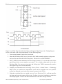
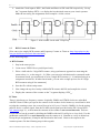
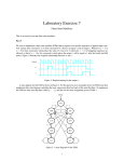
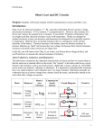
1|P a g e HDL & High Level Synthesize (EEET 2035) Laboratory – II Sequential Circuits with VHDL: DFF, Counter, TFF and Timer Objectives: Develop the behavioural style VHDL code for D-Flip Flop using gated, positive edge and negative edge clock modes Develop the Behavioural style VHDL code for 4-bit counter Develop the structural style VHDL code for 4-bit counter using T Flip Flop (use of generate statement, area-performance analysis after synthesize) Compile, synthesize and simulate each design entity and verify the functionality by creating vector waveform file Verify the circuit mapping by using technology viewer facility in Quartus Requirements: Standard PC with Quartuss-II software Altera DE-I board (Device: EP2C20F484C7) 1. Experimental Setup 1.1 D-type storage elements Digital circuits are major classified as combinational and sequential. The prime difference between two is one rely on present input values (combinational) and other on previous as well as present input values (sequential). Due to nature of storing previous values sequential circuits are also termed as memory elements. A single memory element is itself, a single sequential system that stores 1 bit of information. Any memory element has two stable states corresponding to its storing either a 0 or a 1. A flip-flop is a memory element whose output can change only at the time of its clock’s transition (edge). Synchronous and asynchronous terms are used in respect to the inputs of sequential systems. Sequential system operated at triggering of clock edge (i.e., positive or negative) are termed as synchronous inputs. Whereas sequential systems output changes regardless of the clock input i.e., preset, reset etc, is known as asynchronous inputs. Reset, preset etc can also be associated with clock edge (i.e., positive or negative) so called synchronous inputs some times. A pulse is a short duration change in a signal’s value called transition. Pulse transition from 1 to 0 is known as negative edge and pulse transition from 0 to 1. Signal transition is also known as edge. A clock signal is a train (sequence) of pulses used as a timing signal for the sequential system testing, generally. Sequential systems can be tested at positive edge of the clock (i.e., o to 1) or negative edge of the clock (i.e., 1 to 0). The third category is known as clocked or gated circuits where a sequential element is sensitive to its clock’s level. The circuit below contains three different types of storage element: a gated (transparent) D latch, a positive-edge triggered and negative edge triggered D-type flip-flops. Advanced FPGA Based System Design - Lab II : Sequential Circuits Prepared By: Dr. Tayab Din Memon 2|P a g e Figure 1(a): D Flip Flop (Gated, Positive Edge and Negative Edge) Figure 1(b): Timing Diagram for the verification of the circuit functionality. Do the following setup: 1. Create a new Quartus II project for your circuit. 2. Name the file and top entity as per your desire like; latch (remember again top entity name and your file name must be same in first place). The device is an EP2C20F484C7. 3. Write a VHDL file that instantiates the three storage elements. You can use the code for the gated D-type below as an example to get started. Use a similar coding style for the other flip-flops (Hint: You can use rising_edge and falling_edge VHDL statements for positive and negative edge of the clock transitions). 4. Compile your code and use the Technology Viewer (Tools –> Netlist Viewer –> Technology Map Viewer) to examine the implemented circuit and to determine how the synthesis process has allocated your circuit to the internal resources in the FPGA. 5. Using the waveform below as a guide, create a Vector Waveform File (.vwf) that specifies the inputs and expected outputs of the circuit. Perform a functional simulation to obtain the three output signals. Observe the different behaviour of the three storage elements. Advanced FPGA Based System Design - Lab II : Sequential Circuits Prepared By: Dr. Tayab Din Memon 3|P a g e 6. Note: you would need to write separate process statements for each DFF. 7. When you finish this part jump to part-2 that is related to the development of the counter. LIBRARY IEEE; USE ieee.std_logic_1164.all; ENTITY latch IS PORT (D, Clk: IN STD_LOGIC; Q: OUT STD_LOGIC); END latch; ARCHITECTURE Behavior OF latch IS BEGIN PROCESS (D, Clk) BEGIN IF Clk = ’1’ THEN Q <= D; END IF; END PROCESS; END Behavior; 1.2 Counters 1.2.1 Counters (Behavioural) Counters are sequential circuits that are simple examples of finite state machines. Their behaviour is to count events, generate time intervals, generate events, and divide down an input signal to create a lower frequency output signals. Present state and next state are important terms in counters that describes nothing but what next will appear at output on the clock edge (i.e., positive or negative). A synchronous counter is one in which all the flip-flops are clocked simultaneously by a common clock signal. A straightforward approach to the description of a counter involves use of arithmetic operators. An up counter increments the count at each clock edge and down counter does opposite of it. Counters operate properly when they are initialized with any value (generally ‘0’). Here we will consider two steps experimental setup on counters. Initially we will examine the sixteen-bit counter description with behavioural style of VHDL coding. Do the following steps: 1. Create a new vhdl file in the same project (File –>New –> VHDL file) 2. Copy and paste the vhdl code given below. Save it with a name as entity’s name (i.e., sixteen in this case). 3. Upto now top-level entity of your project is latch.vhd. Change it with sixteen.vhd as counter circuit can be analysed. Remember all the vhdl files included in your project are compiled but you can simulate only one that would be your top-level entity. That’s why you need to make sure the required vhdl file is top-level entity every time. 4. Now compile your project 5. Determine the maximum operating frequency (FMAX) for the circuit (timing simulation –> report) 6. Use the Technology Viewer to examine the implemented circuit and determine how many Logic Elements have been used or you can see this number in the compilation report as well. Advanced FPGA Based System Design - Lab II : Sequential Circuits Prepared By: Dr. Tayab Din Memon 4|P a g e 1. 2. 3. 4. 5. 6. 7. 8. 9. 10. 11. 12. 13. 14. 15. 16. 17. 18. 19. 20. 21. 22. LIBRARY IEEE; USE IEEE.STD_LOGIC_1164.ALL; USE IEEE.NUMERIC_STD.ALL; ENTITY HEX_COUNTER IS PORT (CLK, RST, ENB: IN STD_LOGIC; COUNTER: OUT STD_LOGIC_VECTOR (3 DOWNTO 0)); END HEX_COUNTER; ARCHITECTURE BEHAVIORAL OF HEX_COUNTER IS BEGIN COUNT_PROC: PROCESS (CLK, RST) VARIABLE COUNT: UNSIGNED (3 DOWNTO 0); BEGIN IF (RST='0') THEN COUNT: = (OTHERS => '0'); ELSIF (RISING_EDGE (CLK) AND ENB='1') THEN COUNT: = COUNT + 1; END IF; COUNTER <= STD_LOGIC_VECTOR (COUNT); END PROCESS COUNT_PROC; END BEHAVIORAL; Figure 2– HEX Counter 1.2.2 Counters (Structural) The figure below (figure 3) shows a 4-bit synchronous counter which uses four T-type (toggle) flipflops. Here counter increments on each positive edge of the clock if the enable signal is asserted. The counter is reset to 0 by using the Reset signal. Do the following steps: 1. Stay with the same project 2. Create a new VHDL file as you did previously. 3. Write a VHDL description of a single T-type and save it with a suitable name like TFF or any one as you desire. Remember: you would need to use this vhdl file as a component in the main counter file in next step because we are working in structural mode as we worked in lab-1 part-3 4. Again create a new VHDL file for the counter as shown in figure 3. 5. Create a structural description of a multi-bit counter using your T-type, use a loop— generate construct and a generic to specify the size of the counter. Here you would need instantiate your T-type FF vhdl entity that you created in steps 1 – 3. 6. Set the size at 16 and compile the circuit 7. Determine the number of logic elements that are used in the FPGA. What is the maximum operating frequency (FMAX) for this circuit? 8. Repeat this for counter sizes of 4 and 8. What is the relationship between size and FMAX? How does its performance compare with the previous behavioural version? Advanced FPGA Based System Design - Lab II : Sequential Circuits Prepared By: Dr. Tayab Din Memon 5|P a g e 9. Attach the Clock input to KEY0, the Enable and Reset to SW1 and SW0 respectively. Set up the 7-segment displays HEX3—0 to display the hexadecimal count as your circuit operates. Make the necessary pin assignments and recompile a 16-bit version. Figure 3: 4-bit counter circuit with T-Flip Flop 1.3 BCD Counter & Timer [You can review simply BCD counter and Frequency Counter or Timer at: http://hyperphysics.phyastr.gsu.edu/hbase/electronic/bincount.html] Do the following steps: A. BCD Counter 1. Stay in the same project 2. Create a new VHDL file as you did previously 3. Write a vhdl code for 3-digit BCD counter, using synchronous approach to truncating the count values (i.e., to the range 0—9). [Hint: you can write in behavioural or structural mode. In structural mode you would need to write a single BCD counter (0 – 9) and then bring it as component in main file. In behavioural mode, you can write a single process for all 3-digit BCD counters using if-else statement]. 4. Save the file with an entity name. 5. Now change the top-level entity with this BCD counter vhdl file and compile the circuit 6. Display the contents of the counter on the 7-segment displays, HEX2−0. B. Timer Timer is also known as frequency counter. Originally 50MHz and 27MHz clocks are embedded with DE-I board. When you operate the counter circuit at these clocks human eye would not be able to judge the counting events. An event will occur in 0.02 sec if clock is 50MHz. So for the testing purpose derive a control signal, from the 50-MHz clock signal provided on the DE-1 board (DE-1 user manual page 31), to increment the contents of the counter at one-second intervals. This onesecond interval can be created by dividing the 50MHz with itself. It will give us 1sec clock. Use the pushbutton switch KEY0 to asynchronously reset the counter to 0. Simulate to verify its behaviour. Set up the pin assignments, recompile and download to the board. Observe the outputs as the counter operates. Do the following steps in this regards: Advanced FPGA Based System Design - Lab II : Sequential Circuits Prepared By: Dr. Tayab Din Memon 6|P a g e 1. Stay in the same project 2. Create a new VHDL file as you did previously 3. Write a vhdl code for timer i.e., frequency counter that generate a control signal of 1sec 4. Save the file with an appropriate entity name 5. Now you would need to instantiate this entity into the BCD counter VHDL main file as it can be hooked-up with BCD counter clock 6. The top-level entity will remain same as we are not using timer as main file it is just helping us to derive the BCD counter with 1-sec (i.e., every count would appear in 1sec). 7. Display the contents of the counter on the 7-segment displays, HEX2−0. 8. NB: If you want to derive the BCD counter with 0.5 second, what number you would need to divide the clock? Advanced FPGA Based System Design - Lab II : Sequential Circuits Prepared By: Dr. Tayab Din Memon