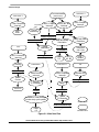
1
3-Phase BLDC Drive Using Variable DC Link
Six-Step Inverter
Designer Reference Manual
56800E
16-bit Digital Signal Controllers
DRM078
Rev. 1
05/2006
freescale.com
3-Phase BLDC Drive Using DC/DC Inverter
Designer Reference Manual
by: Jaroslav Musil
Freescale Czech Systems Laboratories
Roznov pod Radhostem, Czech Republic
To provide the most up-to-date information, the revision of our documents on the World Wide Web will be
the most current. Your printed copy may be an earlier revision. To verify you have the latest information
available, refer to:
http://www.freescale.com
The following revision history table summarizes changes contained in this document. For your
convenience, the page number designators have been linked to the appropriate location.
Revision History
Date
Revision
Level
March,
2006
0
Initial release
1
Changed hybrid controller to digital signal controller
Changed DC/DC inverter to variable DC link six-step inverter
Minor edits to clarify Chapter 1
Renamed Section 2.4 to better reflect contents and added information at end
of section
May, 2006
Description
Page
Number(s)
N/A
Various
Various
7
17
3-Phase BLDC Drive Using Variable DC Link Six-Step Inverter, Rev. 1
Freescale Semiconductor
3
Revision History
3-Phase BLDC Drive Using Variable DC Link Six-Step Inverter, Rev. 1
4
Freescale Semiconductor
Table of Contents
Chapter 1
Introduction
1.1
1.2
Introduction . . . . . . . . . . . . . . . . . . . . . . . . . . . . . . . . . . . . . . . . . . . . . . . . . . . . . . . . . . . . . . . . . 7
Freescale Controller Advantages and Features . . . . . . . . . . . . . . . . . . . . . . . . . . . . . . . . . . . . . 7
Chapter 2
Control Theory
2.1
2.2
2.3
2.4
BLDC Motor . . . . . . . . . . . . . . . . . . . . . . . . . . . . . . . . . . . . . . . . . . . . . . . . . . . . . . . . . . . . . . . .
BLDC Motor Control Using DC/DC Inverter . . . . . . . . . . . . . . . . . . . . . . . . . . . . . . . . . . . . . . . .
Commutation . . . . . . . . . . . . . . . . . . . . . . . . . . . . . . . . . . . . . . . . . . . . . . . . . . . . . . . . . . . . . . .
Speed Control . . . . . . . . . . . . . . . . . . . . . . . . . . . . . . . . . . . . . . . . . . . . . . . . . . . . . . . . . . . . . .
11
11
13
16
Chapter 3
System Concept
3.1
3.2
3.3
System Specification . . . . . . . . . . . . . . . . . . . . . . . . . . . . . . . . . . . . . . . . . . . . . . . . . . . . . . . . . 17
Application Description . . . . . . . . . . . . . . . . . . . . . . . . . . . . . . . . . . . . . . . . . . . . . . . . . . . . . . . 17
Control Process . . . . . . . . . . . . . . . . . . . . . . . . . . . . . . . . . . . . . . . . . . . . . . . . . . . . . . . . . . . . . 18
Chapter 4
Hardware
4.1
4.2
4.3
4.4
Hardware Implementation . . . . . . . . . . . . . . . . . . . . . . . . . . . . . . . . . . . . . . . . . . . . . . . . . . . . .
MC56F8013 Controller Board . . . . . . . . . . . . . . . . . . . . . . . . . . . . . . . . . . . . . . . . . . . . . . . . . .
3-Phase Power Stage with DC/DC Inverter Lite . . . . . . . . . . . . . . . . . . . . . . . . . . . . . . . . . . . .
Motor Specifications — Example . . . . . . . . . . . . . . . . . . . . . . . . . . . . . . . . . . . . . . . . . . . . . . . .
21
22
23
24
Chapter 5
Software Design
5.1
Introduction . . . . . . . . . . . . . . . . . . . . . . . . . . . . . . . . . . . . . . . . . . . . . . . . . . . . . . . . . . . . . . . .
5.2
Main Data Flow Chart . . . . . . . . . . . . . . . . . . . . . . . . . . . . . . . . . . . . . . . . . . . . . . . . . . . . . . . .
5.2.1
Speed Control . . . . . . . . . . . . . . . . . . . . . . . . . . . . . . . . . . . . . . . . . . . . . . . . . . . . . . . . . . .
5.2.2
Voltage Control . . . . . . . . . . . . . . . . . . . . . . . . . . . . . . . . . . . . . . . . . . . . . . . . . . . . . . . . . .
5.2.3
Commutation . . . . . . . . . . . . . . . . . . . . . . . . . . . . . . . . . . . . . . . . . . . . . . . . . . . . . . . . . . . .
5.2.4
Velocity Calculation . . . . . . . . . . . . . . . . . . . . . . . . . . . . . . . . . . . . . . . . . . . . . . . . . . . . . . .
5.3
Software Implementation . . . . . . . . . . . . . . . . . . . . . . . . . . . . . . . . . . . . . . . . . . . . . . . . . . . . . .
5.3.1
Initialization . . . . . . . . . . . . . . . . . . . . . . . . . . . . . . . . . . . . . . . . . . . . . . . . . . . . . . . . . . . . .
5.3.2
Interrupts . . . . . . . . . . . . . . . . . . . . . . . . . . . . . . . . . . . . . . . . . . . . . . . . . . . . . . . . . . . . . . .
5.3.3
Drive State Machine. . . . . . . . . . . . . . . . . . . . . . . . . . . . . . . . . . . . . . . . . . . . . . . . . . . . . . .
5.3.3.1
INIT State . . . . . . . . . . . . . . . . . . . . . . . . . . . . . . . . . . . . . . . . . . . . . . . . . . . . . . . . . . . . .
5.3.3.2
STOPPED State . . . . . . . . . . . . . . . . . . . . . . . . . . . . . . . . . . . . . . . . . . . . . . . . . . . . . . . .
25
25
25
27
28
28
29
29
30
31
32
32
3-Phase BLDC Drive Using Variable DC Link Six-Step Inverter, Rev. 1
Freescale Semiconductor
5
Table of Contents
5.3.3.3
RUNNING State . . . . . . . . . . . . . . . . . . . . . . . . . . . . . . . . . . . . . . . . . . . . . . . . . . . . . . . .
5.3.3.4
FAULT State. . . . . . . . . . . . . . . . . . . . . . . . . . . . . . . . . . . . . . . . . . . . . . . . . . . . . . . . . . .
5.4
Scaling of Quantities . . . . . . . . . . . . . . . . . . . . . . . . . . . . . . . . . . . . . . . . . . . . . . . . . . . . . . . . .
5.4.1
Voltage Scaling . . . . . . . . . . . . . . . . . . . . . . . . . . . . . . . . . . . . . . . . . . . . . . . . . . . . . . . . . .
5.4.2
Current Scaling . . . . . . . . . . . . . . . . . . . . . . . . . . . . . . . . . . . . . . . . . . . . . . . . . . . . . . . . . .
5.4.3
PI Controller Parameters . . . . . . . . . . . . . . . . . . . . . . . . . . . . . . . . . . . . . . . . . . . . . . . . . . .
5.4.4
Speed Calculation . . . . . . . . . . . . . . . . . . . . . . . . . . . . . . . . . . . . . . . . . . . . . . . . . . . . . . . .
5.5
FreeMASTER Software . . . . . . . . . . . . . . . . . . . . . . . . . . . . . . . . . . . . . . . . . . . . . . . . . . . . . . .
32
32
33
33
33
34
34
35
Chapter 6
Application Setup
6.1
6.1.1
6.1.2
6.2
6.2.1
6.3
6.4
Application Description . . . . . . . . . . . . . . . . . . . . . . . . . . . . . . . . . . . . . . . . . . . . . . . . . . . . . . .
Control Process . . . . . . . . . . . . . . . . . . . . . . . . . . . . . . . . . . . . . . . . . . . . . . . . . . . . . . . . . .
Drive Protection . . . . . . . . . . . . . . . . . . . . . . . . . . . . . . . . . . . . . . . . . . . . . . . . . . . . . . . . . .
Application Set-Up . . . . . . . . . . . . . . . . . . . . . . . . . . . . . . . . . . . . . . . . . . . . . . . . . . . . . . . . . . .
MC56F8013 Controller Board Application Setup . . . . . . . . . . . . . . . . . . . . . . . . . . . . . . . . .
Project Files . . . . . . . . . . . . . . . . . . . . . . . . . . . . . . . . . . . . . . . . . . . . . . . . . . . . . . . . . . . . . . . .
Application Build and Execute . . . . . . . . . . . . . . . . . . . . . . . . . . . . . . . . . . . . . . . . . . . . . . . . . .
37
37
38
40
41
43
44
3-Phase BLDC Drive Using Variable DC Link Six-Step Inverter, Rev. 1
6
Freescale Semiconductor
Chapter 1
Introduction
1.1 Introduction
This paper describes the design of a 3-phase BLDC drive using a variable DC link six-step inverter, based
on Freescale’s MC56F8013 dedicated motor control device.
Recently, small high-speed BLDC motors have become very popular in a wide application area. The
BLDC motor does not have a mechanical commutator and is, consequently, more reliable than the DC
motor. Small high-speed BLDC motors have very low inductance compared to conventional BLDC
motors. When PWM control is applied to the phases of a BLDC motor, the current follows the rectangular
PWM voltage shape. This rapidly changing current magnetizes and demagnetizes the motor iron at a
frequency equal to the PWM frequency. Due to magnetic hysteresis losses, the motor can become hot
enough to be damaged and the high current ripple will cause other losses. Because of the special control
required by the motor, the method adopted in this reference design uses a variable DC link six-step
inverter r to generate the desired voltage for the motor. The motor then requires only a conventional
three-phase inverter for commutation.
The concept of the application is a high-speed BLDC motor with closed-loop speed-control. It serves as
a design example of a 3-phase BLDC drive with variable DC link six-step inverter, using a Freescale
digital signal controller.
This reference design includes basic motor theory, system design concept, hardware implementation,
and the software design, including the FreeMASTER software visualization tool.
1.2 Freescale Controller Advantages and Features
The Freescale MC56F801x family is well suited to digital motor control, combining the DSP’s calculation
capability with the MCU’s controller features on a single chip. These digital signal controllers offer many
dedicated peripherals such as pulse width modulation (PWM) modules, analog-to-digital converters
(ADC), timers, communication peripherals (SCI, SPI, I2C), and on-board Flash and RAM.
The MC56F801x family members provide the following peripheral blocks:
• One PWM module (although with a limited pinout on the MC56F8014) with PWM outputs, fault
inputs, fault-tolerant design with dead time insertion, supporting both center-aligned and
edge-aligned modes
• 12-bit ADCs, supporting two simultaneous conversions; ADC and PWM modules can be
synchronized
• One dedicated 16-bit general purpose quad timer module
• One serial peripheral interface (SPI)
• One serial communications interface (SCI) with LIN slave functionality
• One inter-integrated circuit (I2C) port
• On-board 3.3V to 2.5V voltage regulator for powering internal logic and memories
3-Phase BLDC Drive Using Variable DC Link Six-Step Inverter, Rev. 1
Freescale Semiconductor
7
Introduction
•
•
•
•
•
•
Integrated power-on reset and low voltage interrupt module
All pins multiplexed with general purpose input/output (GPIO) pins
Computer operating properly (COP) watchdog timer
External reset input pin for hardware reset
JTAG/On-Chip Emulation (OnCE™) module for unobtrusive, processor-speed-independent
debugging
Phase-locked loop (PLL) based frequency synthesizer for the digital signal controller core clock,
with on-chip relaxation oscillator
Table 1-1. Memory Configuration
Memory Type
MC56F8013
MC56F8014
Program Flash
16 Kbyte
16 Kbyte
Unified Data/Program RAM
4 Kbyte
4 Kbyte
BLDC motor control benefits greatly from the flexible PWM module, fast ADC, and quad timer module.
The PWM offers flexibility in its configuration, enabling efficient control of the BLDC motor. The PWM
block has the following features:
• Three complementary PWM signal pairs, six independent PWM signals (or a combination)
• Complementary channel operation features
• Independent top and bottom dead time insertion (56F8013)
• Separate top and bottom pulse width correction via current status inputs or software
• Separate top and bottom polarity control
• Edge-aligned or center-aligned PWM reference signals
• 15-bit resolution
• Half-cycle reload capability
• Integral reload rates from one to sixteen periods
• Mask/swap capability
• Individual, software-controlled PWM output
• Programmable fault protection
• Polarity control
• 10mA or 16mA current sink capability on PWM pins
• Write-protectable registers
The PWM module is capable of controlling two PWM signals for the variable DC link six-step inverter. It
can be configured to a switching frequency of 100kHz with a resolution of 1 in 960, i.e. almost 10-bit. The
PWM module generates its reload signal; it can then be used to synchronize other modules to the PWM.
The four remaining PWM channels are used for phase A and phase B of the 3-phase inverter, which takes
care of the motor commutation using the mask feature of the DSC. Phase C is controlled by two GPIO
pins.
3-Phase BLDC Drive Using Variable DC Link Six-Step Inverter, Rev. 1
8
Freescale Semiconductor
Freescale Controller Advantages and Features
The ADC module has the following features:
• 12-bit resolution
• Dual ADCs per module; three input channels per ADC
• Maximum ADC clock frequency of 5.33MHz with a 187ns period
• Sampling rate of up to 1.78 million samples per second
• Single conversion time of 8.5 ADC clock cycles (8.5 x 187ns = 1.59ms)
• Additional conversion time of six ADC clock cycles (6 x 187ns = 1.125ms)
• Eight conversions in 26.5 ADC clock cycles (26.5 x 187ns = 4.97ms) using parallel mode
• Ability to use the SYNC input signal to synchronize with the PWM (provided the integration allows
the PWM to trigger a timer channel connected to the SYNC input)
• Ability to sequentially scan and store up to eight measurements
• Ability to scan and store up to four measurements on each of two ADCs operating simultaneously
and in parallel
• Ability to scan and store up to four measurements on each of two ADCs operating asynchronously
to each other in parallel
• Interrupt generating capabilities at the end of a scan when out-of-range limit is exceeded and on
zero crossing
• Optional sample correction by subtracting a pre-programmed offset value
• Signed or unsigned result
• Single-ended or differential inputs
• PWM outputs with hysteresis for three of the analog inputs
The ADC is used to measure DC bus voltage, variable DC link six-step inverter output voltage, DC bus
current, and +0.2V voltage and +1.65V current references.
The application uses the ADC block in simultaneous mode scan. It is synchronized to the PWM pulses.
This configuration allows the simultaneous conversion of the required analog values of current and
voltage within the required time.
The quad timer is an extremely flexible module, providing all required services relating to time events. It
has the following features:
• Four 16-bit counters/timers
• Count up/down
• Counters are cascadable
• Programmable count modulus
• Maximum count rate equal to the peripheral clock/2, when counting external events
• Maximum count rate equal to the peripheral clock/1, when using internal clocks
• Count once or repeatedly
• Counters are preloadable
• Counters can share available input pins
• Each counter has a separate prescaler
• Each counter has capture and compare capability
3-Phase BLDC Drive Using Variable DC Link Six-Step Inverter, Rev. 1
Freescale Semiconductor
9
Introduction
The application uses four channels of the quad timer for:
• PWM-to-ADC synchronization
• Hall sensor edge scanning used for speed calculation
• System base for ramp and speed control
• Commutation advance control
3-Phase BLDC Drive Using Variable DC Link Six-Step Inverter, Rev. 1
10
Freescale Semiconductor
Chapter 2
Control Theory
2.1 BLDC Motor
A brushless DC (BLDC) motor is a rotating electric machine where the stator is a classic 3-phase stator,
like that of an induction motor, and the rotor has surface-mounted permanent magnets (see Figure 2-1).
Stator
Stator winding
(in slots)
Shaft
Rotor
Air gap
Permanent magnets
Figure 2-1. BLDC Motor — Cross Section
In this respect, the BLDC motor is equivalent to a reversed DC commutator motor, in which the magnet
rotates while the conductors remain stationary. In the DC commutator motor, the current polarity is altered
by the commutator and brushes. On the contrary, in the brushless DC motor, the polarity reversal is
performed by power transistors switching in synchronization with the rotor position. Therefore, BLDC
motors often incorporate either internal or external position sensors to discern the actual rotor position;
alternatively, the position can be detected without sensors.
2.2 BLDC Motor Control Using a Variable DC Link Six-Step Inverter
The BLDC motor is driven by rectangular voltage waveforms coupled with the given rotor position (see
Figure 2-2). The generated stator flux interacts with the rotor flux generated by a rotor magnet, defining
the torque, and thus speed, of the motor. The voltage waveforms must be properly applied to the two
phases of the 3-phase winding system, to keep the angle between the stator flux and the rotor flux close
to 90° to generate maximum torque. To achieve this, the motor requires electronic control for proper
operation.
3-Phase BLDC Drive Using Variable DC Link Six-Step Inverter, Rev. 1
Freescale Semiconductor
11
Control Theory
Voltage
+UDCB
Phase A
-UDCB
+UDCB
Phase B
-UDCB
+UDCB
Phase C
-UDCB
30º
60º
90º
120º
150º
180º
210º
240º
270º
300º
3-phase
330º Electrical
angle
Figure 2-2. Voltage Waveforms Applied To the 3-phase BLDC Motor
For standard BLDC motors, a power stage with a 3-phase inverter is used. Control is provided by applying
PWM waveforms to the MOSFETs of the 3-phase inverter. However, there are small high-speed BLDC
motors with very low inductance. If PWM is applied to the MOSFETs of the 3-phase inverter of such a
motor, the current waveform will copy the PWM voltage waveform. Such a current waveform will rapidly
and frequently magnetize and demagnetize the metal causing huge thermal losses due to magnetic
hysteresis. Therefore, these BLDC motors require a special power stage with a variable DC link six-step
inverter, illustrated in Figure 2-3. The power stage uses six power transistors fully turned on/off to control
the commutation. The voltage level is controlled by two transistors in the variable DC link six-step inverter.
Brake
V_PWR
DC/DC Inverter
DCDC_Top
3-ph. Inverter
L
Brake
DCDC_Botom
PWM_AT
PWM_BT
PWM_CT
PWM_AB
PWM_BB
PWM_CB
C
GND_PWR
Phase_A Phase_B Phase_C
Figure 2-3. 3-Phase BLDC Power Stage with a Variable DC Link Six-Step Inverter
3-Phase BLDC Drive Using Variable DC Link Six-Step Inverter, Rev. 1
12
Freescale Semiconductor
Commutation
The variable DC link six-step inverter controls the voltage on the motor, while commutation is performed
by the 3-phase inverter. The variable DC link six-step inverter output is controlled by switching the
DCDC_Top MOSFET (Figure 2-3). Thus, the variable DC link six-step inverter uses the inductor L and
the capacitor C to keep output voltage at the desired level.
This variable DC link six-step inverter can also work in the opposite direction, i.e. during braking, it can
transfer energy to the power supply’s input voltage level. To reduce the load voltage level during motor
braking, the DCDC_Bottom MOSFET is used. If this MOSFET is turned on, the inductor is charged. In the
instant when the MOSFET is turned off, the energy accumulated in the inductor is transferred to the
variable DC link six-step inverter’s input. This temporarily causes a higher voltage at the input. For longer
operations, the input capacitor will not absorb all the energy, and the input voltage will be higher. In this
case, care must be taken, and the braking MOSFET must be turned on while the voltage is higher, to
reduce the voltage to a safe level.
The bottom MOSFET of the variable DC link six-step inverter operates in a different way to the top one,
i.e. whereas the top MOSFET can be switched from 0 to 100% of the duty cycle, the bottom one cannot.
The bottom MOSFET can only be switched from 0 to a certain percentage, because the inductor is
discharged when the MOSFET is turned off. This maximum duty cycle depends on the voltages at both
the input and the output.
The 3-phase inverter energizes two BLDC motor phases at the same time. The third phase is not powered
(see Figure 2-2). Thus, we have six voltage vectors that may be applied to the BLDC motor.
2.3 Commutation
Commutation provides the creation of a rotation field. As explained previously, for proper operation of a
BLDC motor it is necessary to keep the angle between the stator and rotor flux close to 90°. With six-step
control we get a total of six possible stator flux vectors. The stator flux vector must be changed at a certain
rotor position. The rotor position is usually sensed by Hall sensors. The Hall sensors generate three
signals also comprising six states. Each of the Hall sensor states corresponds to a certain stator flux
vector. All Hall sensor states with corresponding stator flux vectors are illustrated in Figure 2-4. The same
figure is illustrated in tables Table 2-1 and Table 2-2.
The next two figures depict the commutation process. The actual rotor position in Figure 2-5 corresponds
to the Hall sensors’ state ABC[110] (see Figure 2-4). The actual voltage pattern can be derived from the
Table 2-1. Phase A is connected to the positive DC bus voltage by the transistor PWM_AT, phase C is
connected to ground by transistor PWM_CB, and phase B is not powered.
As soon as the rotor reaches a certain position (see Figure 2-5), the Hall sensor state changes its value
from ABC[110] to ABC[100]. From Table 2-1 a new voltage pattern is selected and applied to the BLDC
motor.
As can be seen, with a six-step control technique there is no possibility of keeping the angle between the
rotor flux and the stator flux precisely at 90°. The real angle varies from 60° to 120°.
The commutation is repeated for each 60 electrical degrees. The angular (time) accuracy of the
commutation event is critical; any deviation causes torque ripples leading to variations in speed.
3-Phase BLDC Drive Using Variable DC Link Six-Step Inverter, Rev. 1
Freescale Semiconductor
13
Control Theory
Figure 2-4. Stator Flux Vectors with Six-Step Control
Table 2-1. Commutation Sequence for Clockwise Rotation
Hall Sensor A
Hall Sensor B
Hall Sensor C
Phase A
Phase B
Phase C
1
0
0
–VDCB
+VDCB
NC
1
0
1
NC
+VDCB
–VDCB
0
0
1
+VDCB
NC
–VDCB
0
1
1
+VDCB
–VDCB
NC
0
1
0
NC
–VDCB
+VDCB
1
1
0
–VDCB
NC
+VDCB
Table 2-2. Commutation Sequence for Counterclockwise Rotation
Hall Sensor A
Hall Sensor B
Hall Sensor C
Phase A
Phase B
Phase C
1
0
0
+VDCB
–VDCB
NC
1
1
0
+VDCB
NC
–VDCB
0
1
0
NC
+VDCB
–VDCB
0
1
1
–VDCB
+VDCB
NC
0
0
1
–VDCB
NC
+VDCB
1
0
1
NC
–VDCB
+VDCB
3-Phase BLDC Drive Using Variable DC Link Six-Step Inverter, Rev. 1
14
Freescale Semiconductor
Commutation
Figure 2-5. Situation Right Before Commutation
Figure 2-6. Situation Right After Commutation
3-Phase BLDC Drive Using Variable DC Link Six-Step Inverter, Rev. 1
Freescale Semiconductor
15
Control Theory
2.4 Speed and Voltage Control
Commutation ensures proper rotor rotation of the BLDC motor, while the motor speed depends only on
the amplitude of the applied voltage. The amplitude of the applied voltage is adjusted by the variable DC
link six-step inverter using pulse width modulation. The required speed is controlled by a speed controller.
The speed and voltage controllers are implemented as conventional PI controllers. The difference
between the actual and required speed (voltage) is the input to the PI controller. Using this difference, the
PI controller controls the duty cycle of PWM pulses fed to the variable DC link six-step inverter,
corresponding to the voltage amplitude required to keep the desired speed. See Figure 2-7.
M
+
Desired
Speed
Σ
-
Speed
Controller
+
Σ
-
Voltage
Controller
DC/DC
Inverter
3-ph.
Inverter
Actual Voltage
Actual Speed
PWM
Generator
Commutation
Hall Sensors
Figure 2-7. Speed Control
The speed controller calculates output voltage u(t) using a proportional-integral (PI) algorithm, in
accordance with the following equations:
1 t
u ( t ) = K c e ( t ) + ----- ∫ e ( τ ) dτ
TI 0
(2-1)
After transformation to a discrete time domain using an integral approximation by a Backward Euler
method, we get the following equations for the numerical PI controller calculation:
(2-2)
u( k )= u ( k ) + u ( k )
P
I
uP ( k ) = Kc ⋅ e ( k )
(2-3)
T
u I ( k ) = u I ( k – 1 ) + K c ----- ⋅ e ( k )
TI
(2-4)
where:
e(t)
=
Input error in time t
up(k)
=
Proportional output portion in step k
e(k)
=
Input error in step k
uI(k)
=
Integral output portion in step k
w(k)
=
Desired value in step k
uI(k-1)
=
Integral output portion in step k-1
m(k)
=
Measured value in step k
TI
=
Integral time constant
u(t)
=
Controller output in time t
=
Sampling time
u(k)
=
Controller output in step k
T
Kc
=
Controller gain
3-Phase BLDC Drive Using Variable DC Link Six-Step Inverter, Rev. 1
16
Freescale Semiconductor
Speed and Voltage Control
The voltage controller calculates the output PWM duty cycle for the variable DC link six-step inverter using
the same proportional-integral (PI) algorithm as the speed controller.
3-Phase BLDC Drive Using Variable DC Link Six-Step Inverter, Rev. 1
Freescale Semiconductor
17
Control Theory
3-Phase BLDC Drive Using Variable DC Link Six-Step Inverter, Rev. 1
18
Freescale Semiconductor
Chapter 3
System Concept
3.1 System Specification
The system is designed to drive a 3-phase BLDC motor. The application meets the following performance
specification:
• Voltage control of BLDC motor using Hall sensors
• Targeted at the MC56F8013 controller board
• Running on 3-Phase Power Stage with DC/DC Inverter Lite
• Control technique incorporating:
– Voltage BLDC motor control using variable DC link six-step inverter with voltage closed loop
– Closed-loop BLDC motor speed control
– Both directions of rotation (however, because an impeller is used in the application, the
FreeMASTER page is locked to one direction only)
– Both motor and generator modes
– Starting from any motor position without rotor alignment
– Minimum speed – 300 RPM
– Maximum speed – 38000 RPM
• FreeMASTER software control interface (motor start/stop, speed setup)
• FreeMASTER software monitor
– FreeMASTER software graphical control page (required speed, actual motor speed, start/stop
status, DC bus voltage level, motor current, system status)
– FreeMASTER software speed scope (observes actual and desired speeds)
– FreeMASTER software Hall sensor scope (observes actual Hall sensors’ state)
• DC bus overvoltage and undervoltage, overcurrent, Hall sensors cable fault protection
3.2 Application Description
A standard system concept is chosen for the drive (see Figure 3-1). The system incorporates the following
hardware boards:
• Power supply 24V DC, 5A
• 3-Phase Power Stage with DC/DC Inverter Lite
• BLDC motor with Hall sensors
• MC56F8013 controller board
The 3-Phase Power Stage with DC/DC Inverter Lite runs the main control algorithm. In response to the
user interface and feedback signals, it generates PWM signals for the variable DC link six-step inverter
and 3-phase output signals for a 3-phase inverter.
3-Phase BLDC Drive Using Variable DC Link Six-Step Inverter, Rev. 1
Freescale Semiconductor
19
System Concept
M C56F 8013
Contro ller B oard
V oltage
leve l contro l
Duty c ycle
PW M R eload
Q T_3
50kH z
V oltage
P I Controlle r
Voltage
D igital
filtering
Advance
D esired
voltage
C om m utation
Hand ler
S peed
P I Controlle r
S peed
Calculation
S peed
Ramp
1kH z
M O S FE T
P redrive r
G P IO _B 1
P W M _4
P W M _5
P ower
input
5V
3.3V
D C/D C
Inverter
M O S FE T
P redrive r
Trigger
50kH z
Voltage, current
ADC
Q T_1
P W M _0-3
G P IO _A 6
G P IO _B 3
3-p h . Pow er Stage w ith
D C /D C In ve rter Lite
M O S FE T
P redrive r
Freem aster
S CI
Interrupt
Application
State M achine
Q T_2
G P IO _B 0
3-phase
Inverter
H all sen sors
M
Q T_0
Speed
com m and
Pow er
Supply
B rake
Res istance
100kH z
G P IO _B 5
G P IO _B 2
Actual
speed
D esired
speed
15V
P ower
input
R S232
PC
FreeM A S TE R
Predriver
on/off
Figure 3-1. System Concept
3.3 Control Process
The state of the user interface is scanned periodically, while the speed of the motor is measured on each
new arriving edge from the Hall sensors (only one phase is used for speed measurement). The speed
command is calculated, according to the state of the control signals (Start/Stop, Speed from
FreeMASTER). Then the speed command is processed by means of the speed ramp algorithm. The
comparison between the actual speed command obtained from the ramp algorithm output and the
measured speed generates a speed error. The speed error is input to the speed PI controller, generating
a new desired voltage level for the voltage PI controller. The ADC is used to measure voltage at the
variable DC link six-step inverter output and a digital filter is applied to this value. Then the filtered voltage
is fed to the voltage PI controller. The comparison between the measured and desired voltages generates
a voltage error. The voltage error is input to the voltage PI controller, generating a new duty cycle for the
3-Phase BLDC Drive Using Variable DC Link Six-Step Inverter, Rev. 1
20
Freescale Semiconductor
Control Process
variable DC link six-step inverter. The duty cycle value creates the PWM output for the variable DC link
six-step inverter, and the commutation algorithm creates the output signals for the 3-phase inverter.
The Hall sensor signals are scanned independently of the speed control. Each new arriving edge of any
Hall sensor signal calls the interrupt routine, providing the commutation algorithm. From a certain speed
level the routine determines if the incoming Hall sensor edge is correct, by comparing it with a predicted
signal.
As there is a delay between the Hall sensor edge and current commutation, the current is not symmetrical.
To keep the current symmetrical, a so-called commutation advance is generated. The commutation is
applied using a timer countdown. The timer countdown period is calculated using the time between two
particular commutation edges in the previous step, i.e. there is a table of times for each commutation
sector. Owing to motor geometry inaccuracy (Hall sensors and winding position), it is necessary to store
timing information for each commutation sector.
In the case of a higher voltage at the variable DC link six-step inverter input, the brake resistance is turned
on to reduce voltage. When the voltage reaches a normal level, the brake resistance is turned off.
In the case of overvoltage, undervoltage, overcurrent or incorrect commutation edges within 200
commutations, the signals for the variable DC link six-step inverter and for the 3-phase inverter are
disabled and the fault state is displayed.
3-Phase BLDC Drive Using Variable DC Link Six-Step Inverter, Rev. 1
Freescale Semiconductor
21
System Concept
3-Phase BLDC Drive Using Variable DC Link Six-Step Inverter, Rev. 1
22
Freescale Semiconductor
Chapter 4
Hardware
4.1 Hardware Implementation
The application runs on Freescale’s motor control MC56F8013 Controller Board, Freescale’s 3-Phase
Power Stage with DC/DC Inverter Lite, and a 24V BLDC motor with Hall sensors and high speed impeller.
Both boards are integral parts of Freescale’s set of embedded motion control development tools. The
application hardware system configuration is shown in Figure 4-1.
B L DB CL D C
to or to r
M oM
M o to r
P hases
H a ll
S e n s o rs
A
J7
J202
3 -p h . P o w e r S ta g e w ith
D C /D C In v e rte r L ite
J206
M C56F8013
C o n tro lle r B o a rd
J201
U N I-3
J1
J6
J a c k 2 .1 m m
P o w e r In p u t
2 4 V /5 .4 A
RS232
Figure 4-1. Hardware System Configuration
3-Phase BLDC Drive Using Variable DC Link Six-Step Inverter, Rev. 1
Freescale Semiconductor
23
Hardware
All system parts are supplied and documented in these references:
• MC56F8013 Controller Board:
Using Freescale’s MC56F8013 as the controller
Supplied as MC56F8013 Controller Board
Described in the MC56F8013 Controller Board User’s Manual
• 3-Phase Power Stage with DC/DC Inverter Lite:
Using Freescale’s MC33883 MOSFET pre-drivers
Supplied as 3-Phase Power Stage with DC/DC Inverter Lite
Described in the 3-Phase Power Stage with DC/DC Inverter User’s Manual
A detailed description of each individual board can be found in the appropriate user manual, or on the
Freescale web site http://www.freescale.com. The user manuals include a schematic of the board, a
description of individual function blocks, and a bill of materials (parts list).
4.2 MC56F8013 Controller Board
The MC56F8013 controller board is based on an optimized PCB and power supply design. It
demonstrates the abilities of the MC56F8013 and provides a hardware tool to help in the development of
applications using the MC56F8013.
The MC56F8013 controller board is an evaluation module type of board; it includes an MC56F8013 part,
encoder interface, tacho-generator interface, communication options, digital and analog power supplies,
and peripheral expansion connectors. The expansion connectors are for signal monitoring and user
feature expandability. Test pads are provided for monitoring critical signals and voltage levels.
The MC56F8013 controller board is designed for the following purposes:
• To allow new users to become familiar with the features of the MC56F801x architecture.
• To serve as a platform for real-time software development. The tool suite allows you to develop
and simulate routines, download the software to on-chip memory, run the software, and debug it
TM
using a debugger via the JTAG/OnCE port. The breakpoint features of the OnCE port let you
specify complex break conditions easily and execute your software at full-speed, until the break
conditions are satisfied. The ability to examine and modify all user accessible registers, memory,
and peripherals through the OnCE port simplifies considerably the task of the developer.
• To serve as a platform for hardware development. The hardware platform enables external
hardware modules to be connected. The OnCE port's unobtrusive design means all of the memory
on the digital signal controller chip is available to the user.
The MC56F8013 Controller Board facilitates the evaluation of various features present in the
MC56F8013. The MC56F8013 Controller Board can be used to develop real-time software and hardware
products based on the MC56F8013. The MC56F8013 Controller Board provides the features necessary
to write and debug software, demonstrate the functionality of that software, and to interface with the
customer's application specific device(s). The MC56F8013 Controller Board is flexible enough to allow full
exploitation of the MC56F8013's features to optimize the performance of the user’s end product. See
Figure 4-2.
3-Phase BLDC Drive Using Variable DC Link Six-Step Inverter, Rev. 1
24
Freescale Semiconductor
3-Phase Power Stage with DC/DC Inverter Lite
MC56F8013
JTAG
Header
JTAG / OnCE /
GPIO PD
ADC
HEADER
PWM
HEADER
PWM LEDs
B2, B4, B5, B6
UNI-3
expansion
connector
PWM / GPIO PA
ADC / GPIO PC
Protection
Logic
FAULT 0 / GPIO PA6
RESET / GPIO PA7
GPIO PB
Buttons
& Switch
B0, B1, B3
UNI-3
expansion
connector
B6
User LED
B4, B5, B6
+3.3V Analog
Power Supply
VDDA ADC
+3.3V Digital
Power Supply
VDD IO
Encoder Interface
Tacho-Generator
Interface
B4
B6, B7
RS 232
Interface
B0, B1
EEPROM
Interface
+5V Power
Supply
+12V Power
Supply
GPIO PB
HEADER
SPI
HEADER
SCI
HEADER
Figure 4-2. Block Diagram of the MC56F8013 Controller Board
4.3 3-Phase Power Stage with DC/DC Inverter Lite
Freescale Semiconductor’s embedded motion control series 3-Phase Power Stage with DC/DC Inverter
Lite is a 12V – 42V, 10A, surface-mount power stage. In combination with one of the embedded motion
control series control boards, it provides a software development platform allowing algorithms to be
written and tested without the need to design and build a power stage. It supports algorithms that use Hall
sensors, and encoder and back EMF (electromotive force) signals for sensorless control.
The 3-Phase Power Stage with DC/DC Inverter Lite does not have any overcurrent protection
independent of the control board; therefore, care in its setup and use is required if a lower impedance
motor is used. Current measuring circuitry is set up for ±14.025A full scale. In a 25° ambient operation at
up to 9A continuous RMS (12A for 10 seconds), output current is within the board’s thermal limits.
Input connections are made via 40-pin ribbon cable connector J201. Power connections to the motor are
made on a 3-way output connector J202. Phase A, phase B, and phase C are labeled on the board. The
input current requirements are met by a single DC power supply capable of supplying 5A; however, it is
recommended to use a more powerful supply. The voltage requirements are met by a power supply of
12V – 42V. The voltage should be within these limits. The board will sustain at least 9V, with maximum
3-Phase BLDC Drive Using Variable DC Link Six-Step Inverter, Rev. 1
Freescale Semiconductor
25
Hardware
of 50V (depending on the populated components rating). The input power is supplied by means of a
2.1mm jack connector J206.
Table 4-1. Electrical Characteristics of the Power Stage
Characteristic
Symbol
Min
Typ
Max
Units
Vdc
9
12, 24, 42
50
V
ICC
—
1.7
—
mA
ICC5V
—
4.8
—
mA
ICC15V
—
5.9
—
mA
ICCSPL
—
8.9
—
mA
ICCALL
—
30.0
—
mA
Min Logic 1 Input Voltage
VIH
2.4
—
—
V
Max Logic 0 Input Voltage
VIL
—
—
0.8
V
Input Logic Resistance
RIn
—
4.7
—
kΩ
Analog Output Range
VOut
0
—
3.3
V
Bus Current Sense Voltage
ISense
—
118
—
mV/A
Bus Current Sense Offset
Ioffset
Bus Voltage Sense Voltage
VBus
Bus Voltage Sense Offset
Voffset
Power Supply Voltage
Quiescent
Current(1)
Quiescent Current: +5V Generation on
Quiescent Current: +15V Generation
(1)
on(1)
(1)
Quiescent Current: +5V, +15V Generation on
Quiescent Current: +5V, +15V, Drivers On Signal
(1)
Power MOSFET On Resistance
Continuous Output
Current(2)
Pulsed Output Current
Total Power Dissipation (per
MOSFET)(2)
Required Dead Time (generated by processor)
1.65
—
V
153
—
0.2
mV/V
V
RDS(On)
0.25
0.85
1.4
mΩ
ID
—
9
12
A
IDM
—
—
50
A
PD
—
1.85
3.75
W
toff
200
400
—
ns
1. Measured with the input power of 24V.
2. The values are measured at 25°C, for other temperatures the values may be different.
4.4 Motor Specifications — Example
The motor used in this application is a high-speed, low-inductance 24V BLDC motor equipped with Hall
sensors. The motor has the following specifications:
Table 4-2. Specifications of the Motor and Hall Sensors
Motor Specification:
Position Sensor Specification:
Motor Type:
3-Phase BLDC Motor
2-Poles
Speed Range:
< 38000 RPM
Line Voltage:
24V
Phase Current:
<5A
Sensor 1 Type:
3-Phase Hall Sensors
Sensor 2 Type:
None
3-Phase BLDC Drive Using Variable DC Link Six-Step Inverter, Rev. 1
26
Freescale Semiconductor
Chapter 5
Software Design
5.1 Introduction
This section describes the design of the drive’s software blocks. The software description comprises
these topics:
• Main Data Flow Chart
• Software Implementation
• Scaling of Quantities
• FreeMASTER Software
5.2 Main Data Flow Chart
The control algorithm of a closed-loop BLDC drive is described in Figure 5-1. The individual processes
are described in the following sections.
5.2.1 Speed Control
Speed control starts with the mfwOmegaRequiredMech variable. This variable is remotely set within
allowed limits by the FreeMASTER software on a PC. The variable mfwOmegaRequiredMech is fed to
the ramp algorithm periodically performed in the timer compare interrupt. It is calculated every 10ms. The
predefined ramp is 10000 RPM per 100ms. The ramp algorithm generates the fwDesiredSpeed
variable input to the speed PI controller as a reference value. The measured speed provides a second
input to this controller. The difference between these two values is the speed error. The speed PI
controller generates the desired variable DC link six-step inverter output voltage fwDesiredVoltage.
The commutation vector is calculated with respect to the polarity of the desired voltage, while its absolute
value is fed to the voltage PI controller as mfwDesiredDCDCVoltage.
If the actual speed absolute value is smaller than 4600 RPM and the desired voltage is smaller than 2V,
the required speed is set to 0, all bottom MOSFETs are turned on, and the motor is braked (the
muwwZeroDCDCVoltage variable is set to 1).
The system contains two speed PI controllers, one for the range 15000 to 40000 RPM created for an
acceleration of 15000 RPM per 100ms, and a second for the range 0 to 15000 RPM constructed with an
acceleration of 10000 RPM per 300ms. The speed controller is calculated every 1ms. The hysteresis
between these two PI controllers is 1500 RPM, meaning if the speed goes up, the higher speed PI
controller is switched on at the threshold of 15000 RPM, and when the speed goes down, the lower speed
PI controller is switched on at a speed of 13500 RPM.
3-Phase BLDC Drive Using Variable DC Link Six-Step Inverter, Rev. 1
Freescale Semiconductor
27
Software Design
Timer Compare
Interrupt
ADC
Start
Quad Timer 1
POSITION SENSOR
(Hall Sensors)
Quad Timer 3
one phase
only
Timer Compare
Interrupt
GPIO (B2, B5)
Interrupt
Timer 0 Capture
Interrupt
Period
Measuring
muwwHallSensorsState
miwDirectionSpinning
muwlMeasuredPeriod
Next HS State
Prediction
Mask and Swap
Calculation
Speed
Calculation
ADC
Predicted
com. time
mudtPWMState
ADC Conversion
Interrupt
Filtering
mfwOmegaActualMech
PWM
0-3
Timer 1
Update
GPIO
A6, B3
PWM Module
Quad Timer 2
SCI
PWM Reload
Interrupt
Timer Compare
Interrupt
FreeMASTER
mfwDCDCVoltage
Brake
Control
Voltage
PI Controller
GPIO B1
mwwDuty
Variable DC Link Six-Step
inverter duty cycle update
mfwOmegaDesiredMech
Ramp
fwDesiredSpeed
Speed
PI Controller
Software Block
mfwDesiredDCDCVoltage
PWM
4,5
Hardware Block
Figure 5-1. Main Data Flow
3-Phase BLDC Drive Using Variable DC Link Six-Step Inverter, Rev. 1
28
Freescale Semiconductor
Main Data Flow Chart
5.2.2 Voltage Control
The voltage control is based on the PWM reload interrupt established at a frequency of 100kHz, illustrated
in Figure 5-2.
m
u
w
w
A
D
C
T
r
i
g
g
e
r 0
1
0
1
0
T
i
m
e
rI
n
c
r
.
0
9
6
0
1
9
2
0
2
8
8
0
3
8
4
0
T
i
m
eµ
s
0
1
0
2
0
3
0
4
0
P
W
Mr
e
l
o
a
di
n
t
.
T
i
m
e
r3c
o
u
n
t
i
n
g
A
D
Cs
c
a
n
A
D
Ci
n
t
e
r
r
u
p
t
Figure 5-2. Voltage Control Scheduling
As stated, the PWM reload generates an interrupt every 10µs. The reload serves to synchronize some
processes to the variable DC link six-step inverter PWM period:
• The ADC start is situated at 1µs after the beginning of every second PWM period by means of
timer 3. This timer is started at the beginning of the PWM reload period. When timer 3 reaches its
compare period, it triggers the ADC scan. The PWM, timer and ADC are connected on a hardware
level, so no software interaction is required.
• When the ADC measures the desired values, it generates an interrupt where the measured values
are filtered and stored for further processing.
• When the PWM reload interrupt is called, the muwwADCTrigger is inverted (0/1). This variable
determines if the ADC is started in the current PWM period (0) and/or if the voltage PI controller is
calculated (1).
Timer 3 does not contain any routine attached to its interrupt, and serves only to start the ADC conversion
precisely 90 increments after the start of the PWM period. When the ADC finishes the conversion it reads
and filters the measured values. The ADC measurement uses only four channels in the simultaneous
mode due to the shortage of time. So ADC channel 0 is used for the variable DC link six-step inverter
output voltage measurement each ADC period (50kHz), and channel 1 is shared by the DC bus input
voltage and motor current that are then measured at a frequency of 25kHz. Channels 4 and 5 are used
to measure the voltage and current zero references. These two references are read and filtered until the
following PWM reload interrupt, when the voltage PI controller value is not calculated. However, the
filtered references are updated in the ADC offset registers in the period when the voltage PI controller
value is calculated
So, the variable DC link six-step inverter output voltage, DC bus input voltage and motor current are
measured. The measured values are subtracted from the measured references and then filtered. The
subtraction is performed by hardware using the ADC offset registers. If the measured DC bus voltage is
greater than 26V, the braking resistance MOSFET is turned on, and is turned off when the voltage falls
below 25V. If the voltage is higher than 25V or lower than 18V for longer than 100ms, the overvoltage or
undervoltage flag is generated. The overcurrent protection averages the measured current over the
interval of 16384 values. If this averaged current is higher than 3.5A the overcurrent flag is generated.
3-Phase BLDC Drive Using Variable DC Link Six-Step Inverter, Rev. 1
Freescale Semiconductor
29
Software Design
As stated, the voltage PI controller calculation is performed every second PWM reload interrupt routine
call, meaning it is calculated at a frequency of 50kHz (every 20µs). The measured and filtered variable
DC link six-step inverter output voltage is fed to the PI controller. The difference between the desired
voltage mfwDesiredDCDCVoltage and the measured voltage mfwDCDCVoltage is the error. This
controller’s output is just the duty cycle for the variable DC link six-step inverter MOSFETs mwwDuty. Its
absolute value is written either into PWM channel 4 or 5. If it is positive, channel 4 is loaded with the duty
cycle value and channel 5 is loaded with 0; vice versa if it is negative.
5.2.3 Commutation
On each new edge of the Hall sensor signals, a capture interrupt (phase A) and/or a GPIO interrupt
(phase B, C) is called. The interrupt routine saves the actual Hall sensor state to
muwwHallSensorsState. The muwwHallSensorsState variable is input to the mask and swap
calculation, determining the final shape of the output voltage. The output variable mudtPWMState is
written directly to the PWM block, channels 0 to 3, and GPIO A6 and B3. The next task performed by an
interrupt routine is the calculation of the spin direction. The result, miwDirectionSpinning, is used for
the speed calculation.
For speeds greater than 500 RPM, the system calculates the next Hall sensors commutation state in
every commutation interrupt. When the new commutation edge arrives, the system compares it with this
predicted state. If the real Hall sensor edge signal is different from predicted, the interrupt routine ends
and no commutation is performed. This means the commutation is performed as soon as the correct Hall
sensor signal arrives.
This routine also stores in the table the time between two commutation edges. Each commutation sector
has its own table record. If the speed is greater than 11600 RPM, commutation is advanced. Once the
controlled commutation advance technique is turned on, it is turned off when the speed goes below
8700 RPM.
The advance period is set by the muwwCommutationAdvance variable with a precision of 100ns. It is
set to 40µs, meaning the commutation is performed 40µs before the commutation edge arrives. It
improves the motor spinning and torque efficiency. This method uses timer 1, updated and synchronized
on every commutation Hall sensor edge.
If the system does not receive the predicted commutation edge within 200 commutations, a Hall sensors
cable fault is generated. During this period the system commutates using the timer and commutation
times table.
5.2.4 Velocity Calculation
The Hall sensors generate streams of pulses captured (phase A) by the timer 0 input capture function.
The speed can be calculated knowing the timer frequency and the time between two Hall sensor edges.
The application uses the two timers’ frequencies to enlarge the RPM range. The first frequency is 4MHz
for the range 3700 to 38000 RPM; the second frequency is 250kHz for the range 250 to 4700 RPM. The
timer frequency is derived from the 32MHz bus clock by applying the divider. For 4MHz the divider is 8,
and for 250kHz it is 128.
So, this divider is adjusted by the current speed. The motor starts with the divider at 128, allowing the
speed to be measurable from 250 RPM. As the speed goes up, the divider is switched to 8 at the
3700 RPM threshold. The system keeps this divider within the range up to 38000 RPM. When the speed
goes down, the divider is switched to 128 at the 4200 RPM threshold.
3-Phase BLDC Drive Using Variable DC Link Six-Step Inverter, Rev. 1
30
Freescale Semiconductor
Software Implementation
5.3 Software Implementation
The general software diagram incorporates the main routine (Main) entered from reset and the interrupt
states (see Figure 5-3).
The main routine initializes the digital signal controller and the application, then it enters an infinite
background loop. The background loop contains an application state machine.
The following interrupt service routines are utilized:
• PWM reload – voltage PI controller calculation and ADC references processing, PWM update
• ADC conversion complete – reads and filters measured values, braking resistance and fault control
• Timer 0 input capture and overflow – commutation and speed calculation
• GPIO B5 and B2 – commutation
• Timer 2 compare – speed PI controller calculation, ramp calculation
• Timer 1 compare – commutation advance
• SCI – services communication with the FreeMASTER software
Reset
Initialization
Interrupts
Main loop
(State Machine)
Figure 5-3. State Diagram — General Overview
5.3.1 Initialization
The Main routine initializes the DSP:
•
Disables interrupts
•
Initializes PLL
•
Disables COP and LVI
•
Initializes the system integration module
– enables PWM, SCI, timer, ADC modules
– connects the timer 3 input to the PWM reload_sync signal
– sets the timer clock source to 1x bus clock
– sets the PWM clock source to 3x bus clock
•
Initializes GPIO A and B modules
– GPIO A6 and B3 as outputs for PWM 4 and 5 MOSFETs
– GPIO B2 and B5 as inputs for Hall sensor signals
– GPIO B0 as the output for the brake resistance control
3-Phase BLDC Drive Using Variable DC Link Six-Step Inverter, Rev. 1
Freescale Semiconductor
31
Software Design
•
Initializes the SCI for FreeMASTER communication
•
Initializes the interrupt controller
•
Initializes the ADC
•
Initializes timer 3 for ADC sync to PWM reload
•
Initializes timer 1 for commutation advance
•
Initializes timer 0 for commutation and speed evaluation
•
Initializes the PWM module:
– Edged-aligned independent PWM mode, positive polarity
– PWM modulus 960 – defines the PWM frequency as 100kHz
– PWM reload – every opportunity
– Channels 0 – 3 for the 3-phase inverter MOSFETs
– Channels 4 – 5 for the variable DC link six-step inverter MOSFETs
•
Initializes the voltage PI controller parameters
•
Reads the Hall sensors signals and evaluates the rotor position
•
Clears GPIO B pending flags
•
Initializes timer 2 for ramp and speed control algorithms
•
Initializes the speed PI controllers parameters
•
Initializes FreeMASTER
•
Pre-sets the first state as the INIT state
•
Enables the interrupts
5.3.2 Interrupts
The interrupts have the following functions:
• PWM reload interrupt – triggered every PWM reload. On an even occurrence, the ADC zero
references are updated in the ADC offset registers and the voltage PI controller is calculated. PWM
channels 4 and 5 are updated by the duty cycle, calculated by the PI controller. The ADC is enabled
so as to start in the next state. On an odd occurrence, the voltage and current ADC zero references
are read and filtered.
• ADC conversion complete interrupt – the ADC is stopped for the next state. The variable DC link
six-step inverter output voltage is read and filtered. Then, depending on the odd or event state,
either the DC bus input voltage or the motor current is read and filtered. The overvoltage and
undervoltage flags are generated according to the measured voltage level, and/or the overcurrent
flag is generated according to the measured motor current level. Brake resistance is turned on and
off depending on the DC bus voltage level.
• Quad timer 0 interrupt – this interrupt has two sources. One of them is the overflow event. In this
event, the routine will remember that the timer overflowed, as information for further speed
calculation. The other source is the input capture signal. This event is used for commutation and
also for the speed calculation. This routine also saves the Hall sensor edge time of each sensor
and uses it to calculate the time of the next advanced commutation.
• GPIO B interrupt – this interrupt routine has two sources, pins 5 and 2. Both are connected to the
Hall sensor signals and serve for commutation.
3-Phase BLDC Drive Using Variable DC Link Six-Step Inverter, Rev. 1
32
Freescale Semiconductor
Software Implementation
•
•
Quad timer 2 interrupt – this interrupt is generated every 1ms. It generates the speed ramp and
calculates the speed PI controller. It also turns on and off the commutation control features, such
as prediction of the next Hall sensor state and commutation advance control.
Quad timer 1 interrupt – this interrupt occurs when the timer reaches the preset compare value
loaded in the quad timer 0 interrupt. This compare event causes advanced commutation and
calculates the time of the next advanced commutation, for the case where the Hall sensor edge
does not arrive in the next state.
5.3.3 Drive State Machine
The drive can be in one of the following states, illustrated in Figure 5-4, also showing transition conditions
among the drive states.
mintSwitchState = 1
Reset
INIT
State
mintSwitchState = 0
mfwOverCurrent <= TRESHOLD_OVERCURRENT
mwwOverVoltageCounter = 0
mwwUnderVoltageCounter = 0
mintSwitchState = 0
mfwOverCurrent <= TRESHOLD_OVERCURRENT
mwwOverVoltageCounter = 0
mwwUnderVoltageCounter = 0
FAULT
State
mwwOverVoltageCounter >= FAULT_COUNTER_OVER_VOLTAGE
mfwOverCurrent > TRESHOLD_OVERCURRENT
mwwUnderVoltageCounter >= FAULT_COUNTER_UNDER_VOLTAGE
STOPPED
State
mintSwitchState = 0
muwwMissedCommutationsCount >=
FAULT_COUNTER_HALL_SENSORSVOLTAGE
mintSwitchState = 1
RUNNING
State
Figure 5-4. Drive State Machine Transitions
3-Phase BLDC Drive Using Variable DC Link Six-Step Inverter, Rev. 1
Freescale Semiconductor
33
Software Design
5.3.3.1 INIT State
The INIT state initializes several state variables and sets up some peripherals:
• Turns off the MOSFET pre-drivers by GPIO B0
• Disables the MOSFET PWM signals by forcing them into tri-state (PWM 0 – 5, GPIO B2, B5)
• Disables the brake resistance control pin and forces it into tri-state (GPIO B1)
• Resets the required speed, desired variable DC link six-step inverter output voltage, variable DC
link six-step inverter PI controller integral portion, and fault occurrence variables.
• If the switch is turned off and no under or overvoltage or overcurrent condition is present the
STOPPED state is entered.
5.3.3.2 STOPPED State
The application remains in this state as long as the switch is turned off. If an undervoltage, overvoltage
or overcurrent fault is present, the FAULT state is entered. The MOSFET pre-drivers are still turned off
so no voltage should be present at the variable DC link six-step inverter output. The following variables
and peripherals are initialized:
• Resets the required speed and the desired variable DC link six-step inverter output voltage and low
speed PI controller integral portion variables.
• If the switch is turned on, the application enters the RUNNING state. At the same time, the variable
DC link six-step inverter duty cycle variable is set to 0, the MOSFET pre-drivers are switched on
by GPIO B0, all the bottom MOSFETs are turned on and the top MOSFETs are turned off, PWM
and GPIO B2 and B5 outputs are enabled, and the brake resistance output pin is enabled.
5.3.3.3 RUNNING State
The application remains in this state as long as the switch is turned on. If an undervoltage, overvoltage,
overcurrent, or Hall sensor signal fault is present, the FAULT state is entered. The MOSFET pre-drivers
are turned on. In this state, the inverters are controlled and the motor can be driven. If the switch is turned
off, the application enters the STOPPED state. At the same time, the PWM and GPIO B2 and B5 output
pins are disabled, forced into tri-state along with the brake resistance control pin GPIO B0.
5.3.3.4 FAULT State
This state is entered when a fault is generated by an overvoltage, undervoltage, overcurrent, or Hall
sensor signal. In this state, the PWM and GPIO B2 and B5 output pins are disabled, forced into tri-state
along with the brake resistance control pin GPIO B0. The MOSFET pre-drivers are turned off by GPIO
B0. The required speed and desired variable DC link six-step inverter output voltage variables are reset.
If the switch is turned off and no undervoltage, overvoltage or overcurrent condition is present, the INIT
state is entered.
3-Phase BLDC Drive Using Variable DC Link Six-Step Inverter, Rev. 1
34
Freescale Semiconductor
Scaling of Quantities
5.4 Scaling of Quantities
The BLDC motor control application uses a fractional representation for all real quantities except time.
The N-bit signed fractional format is represented using 1.[N-1] format (1 sign bit, N-1 fractional bits).
Signed fractional numbers (SF) lie in the following range:
– 1.0 ≤ SF ≤ +1.0 -2
–[ N – 1 ]
(5-1)
For word and long-word signed fractions, the most negative number that can be represented is -1.0,
whose internal representation is $8000 and $80000000, respectively. The most positive word is $7FFF
or 1.0 - 2-15, and the most positive long-word is $7FFFFFFF or 1.0 - 2-31.
The following equation shows the relationship between real and fractional representations:
Real Value
Fractional Value = -------------------------------------------------Real Quantity Range
(5-2)
where:
• Fractional Value is a fractional representation of the real value [Frac16]
• Real Value is the real value of the quantity [V, A, RPM, etc.]
• Real Quantity Range is the maximum range of the quantity, defined in the application [V, A, RPM,
etc.]
5.4.1 Voltage Scaling
The DC bus voltage and variable DC link six-step inverter output voltage sense is defined by the following
equation:
V MEASURED
voltage = -------------------------------- ⋅ 32767
V MAX
(5-3)
Where:
• voltage = variable of measured voltage
• VMEASURED = measured voltage
• VMAX = max. measurable voltage (VMAX = 31V for the 3-Phase Power Stage with DC/DC Inverter
Lite)
5.4.2 Current Scaling
The motor current sense is defined by the following equation:
I MEASURED
current = ------------------------------ ⋅ 32767
I MAX
(5-4)
Where:
• current = variable of measured current
• IMEASURED = measured current
• IMAX = max. measurable current (IMAX = 14.025A for the 3-Phase Power Stage with DC/DC
Inverter Lite)
3-Phase BLDC Drive Using Variable DC Link Six-Step Inverter, Rev. 1
Freescale Semiconductor
35
Software Design
5.4.3 PI Controller Parameters
The PI controller parameters consists of the gain and gain scale parameters of the proportional and
integral constants. The proportional, or integral gain parameter, lies in the fractional number 0 to 1
(representing 0 to 32767) and the gain scale parameter shifts the particular gain to the right if positive, or
to the left if negative. The gain scale number represents the number of shifts.
The limit parameters represent the minimum and maximum outputs from the PI controller. The output will
be within these limits.
5.4.4 Speed Calculation
The speed coefficient scaling is as follows:
1. The maximum speed of the motor is 36200 RPM, so the software maximum speed is set with small
reserve as
(5-5)
vmax = 38000RPM
And for the lower speed maximum, use the maximum higher speed divided by 8, because a
division by 8 can be performed very easily by register shifting, and is not very time consuming.
Therefore:
38000RPM
vmax_low = ---------------------------- = 4750RPM
8
(5-6)
2. We have to know the number of Hall sensor edges per revolution. The motor has one pole-pair,
meaning six edges per revolution (three rising, three falling for the three Hall sensors). But this
application uses only one Hall sensor, so there should be two edges per revolution. As it is a very
fast motor, it is enough to use just one edge (rising) for the speed calculation. So, the final number
of edges per revolution is one. Therefore:
1
1
position_difference = --------------- = --- = 1
edges
1
(5-7)
3. A 16-bit timer is used, meaning it overflows after 65535 increments. As mentioned above, for the
higher speeds the 8 divider is used, so the frequency is 32MHz/8 = 4MHz. The time period for the
timer overflow is then
65535
65535
max_period = ---------------------------- = ---------------- = 16.38375ms
timer_freq
4MHz
(5-8)
For the lower speed calculations, the frequency is 32MHz/128 = 250kHz.. So the time period for
the timer overflow is then
65535
65535
max_period_low = ---------------------------- = -------------------- = 262.14ms
timer_freq
250kHz
(5-9)
4. Knowing the maximum timer period, we can determine the minimum possible speed in RPM. So
the minimum speed limits are
position_difference
1
vmin = 60s ⋅ mi n – 1 ⋅ ----------------------------------------------------- = 60s ⋅ min – 1 ⋅ ------------------------------ = 3662RPM
max_period
16.38375ms
(5-10)
position_difference
1
vmin_low = 60s ⋅ mi n – 1 ⋅ ----------------------------------------------------- = 60s ⋅ min – 1 ⋅ ------------------------ = 237RPM
max_period_low
262.14ms
(5-11)
3-Phase BLDC Drive Using Variable DC Link Six-Step Inverter, Rev. 1
36
Freescale Semiconductor
FreeMASTER Software
5. Now we can calculate the coefficient for the speed calculation. Signed 16-bit fractional arithmetic
is used, so the maximum number can be 32767. The coefficients are then
vmin
3662RPM
mwwOMEGA_ACTUAL_MECH_CONST = 32767 ⋅ -------------- = 32767 ⋅ ---------------------------- = 3158
vmax
38000RPM
(5-12)
vmin_low
237RPM
mwwOMEGA_ACTUAL_MECH_CONST_LOW = 32767 ⋅ -------------------------- = 32767 ⋅ ------------------------- = 1579
vmax_low
4750RPM
(5-13)
6. The speed is then calculated simply using the information of timer increments between two Hall
sensor edges, so
mwwOMEGA_ACTUAL_MECH_CONST
mfwOmegaActualMech = -----------------------------------------------------------------------------------------------------------------counted_edges
(5-14)
However, since the lower speed limit is set by the higher speed limit divided by 8, the lower speed
result must be divided by 8 (meaning shifted by 3 to the right):
mwwOMEGA_ACTUAL_MECH_CONST_LOW
mfwOmegaActualMech = ------------------------------------------------------------------------------------------------------------------------------------ >> 3
counted_edges
(5-15)
7. And the speed in RPM is as follows: 32767 corresponds to 38000 (vmax), so
mfwOmegaActualMech
speed_in_RPM = ---------------------------------------------------------------- ⋅ vmax
32767
(5-16)
5.5 FreeMASTER Software
The FreeMASTER software was designed to provide an application debugging, diagnostic and
demonstration tool for the development of algorithms and applications. It runs on a PC connected to the
controller board via an RS232 serial cable. A small program resident in the digital signal controller
communicates with the FreeMASTER software to parse commands, return status information to the PC,
and process control information from the PC. FreeMASTER software, executing on a PC, uses part of
Microsoft Internet Explorer as the user interface.
The FreeMASTER software is part of the Freescale Semiconductor Quick Start and may be selectively
installed during the Quick Start installation.
The baud rate of the SCI communication for this application is 14400 baud. It is set automatically by the
FreeMASTER software driver and can be changed if necessary.
A detailed description of the FreeMASTER software is provided in the dedicated FreeMASTER for
Embedded Applications documentation.
The 3-phase BLDC motor control application utilizes FreeMASTER software for remote control from the
PC. It enables the user to:
• Control starting and stopping
• Set the motor speed
3-Phase BLDC Drive Using Variable DC Link Six-Step Inverter, Rev. 1
Freescale Semiconductor
37
Software Design
Variables read by the FreeMASTER software and displayed to the user are:
• Required motor speed and actual motor speed
• Application operational mode
• Start/stop status
• DC bus voltage, variable DC link six-step inverter output voltage, motor current
• Overvoltage, undervoltage, overcurrent and Hall sensor cable faults
• Hall sensor state using the on-line scope (The Hall sensor state must be watched at very low
speeds because of the RS232 serial communication speed limitation.)
The FreeMASTER software Control Page is illustrated in Figure 6-1. The profiles of the required and
actual speeds are available in the Speed Scope window.
3-Phase BLDC Drive Using Variable DC Link Six-Step Inverter, Rev. 1
38
Freescale Semiconductor
Chapter 6
Application Setup
6.1 Application Description
The application runs on the Freescale MC56F8013. The software generates all signals needed to control
the variable DC link six-step inverter and 3-phase inverter according to the user-required inputs,
measured and calculated signals.
The concept of the BLDC drive incorporates the following hardware components:
• BLDC motor set
• 3-Phase Power Stage with DC/DC Inverter Lite
• MC56F8013 Controller Board
The BLDC motor incorporates a 3-phase 24V BLDC motor with an attached high-speed impeller. The
BLDC motor has two poles. The Hall sensors are mounted inside the motor. The detailed motor
specifications are listed in Table 4-2.
The drive can be controlled from the FreeMASTER software only:
• To start/stop the drive application, click on the On/Off switch.
• Set the required speed by clicking on the speed gauge.
Measured quantities:
• DC bus voltage
• Motor current
• Rotor speed
The faults used for drive protection:
• Overvoltage
• Undervoltage
• Overcurrent
• Hall sensors cable error
6.1.1 Control Process
After reset, the drive enters the INIT state, in which the application is initialized; it then goes into the STOP
state. In the STOP state, all the control signals are disabled and the motor cannot spin. The operation
mode can be changed to the RUN state from the FreeMASTER software by clicking on the On/Off button.
Speed is controlled in the RUN state using the mfwOmegaRequiredMech variable. This variable is set
within allowed limits remotely by the FreeMASTER software on PC. The variable
mfwOmegaRequiredMech is fed to the ramp algorithm. The predefined ramp is 10000 RPM per 100ms.
The ramp algorithm generates the fwDesiredSpeed variable input to the speed PI controller as a
reference value, and a second input to this controller is the measured speed. The difference between
these two values is the speed error. The speed PI controller generates the desired variable DC link
3-Phase BLDC Drive Using Variable DC Link Six-Step Inverter, Rev. 1
Freescale Semiconductor
39
Application Setup
six-step inverter output voltage fwDesiredVoltage. The commutation vector is calculated with respect
to the polarity of the desired voltage, while its absolute value is fed to the voltage PI controller as
mfwDesiredDCDCVoltage.
The system measures the variable DC link six-step inverter output voltage fed to the PI controller. The
difference between the desired voltage mfwDesiredDCDCVoltage and the measured voltage
mfwDCDCVoltage is the error. This controller’s output is simply the duty cycle for the variable DC link
six-step inverter MOSFETs mwwDuty. Its absolute value is written either to PWM channel 4 or 5. If it is
positive, channel 4 is loaded with the duty cycle value and channel 5 is loaded with 0; vice versa if it is
negative.
According to the Hall sensor state, and the desired direction of spinning, the MOSFETs of the 3-phase
inverter are turned on and off and the motor spins.
6.1.2 Drive Protection
The DC bus voltage and motor current are measured during the control process. They protect the drive
from overvoltage, undervoltage and overcurrent. All protection is performed by software.
The Hall sensor cable signals are read during running. If the sensors return an unidentified commutation
vector, a Hall sensor cable fault is generated.
If any of the above mentioned faults occur, the variable DC link six-step inverter and 3-phase inverter
control signals are disabled to protect the drive, and the application enters the FAULT state. At the same
time, the MOSFET pre-drivers are disabled. If no overvoltage, undervoltage or overcurrent condition is
present, the application can be switched from the FAULT state to the STOP state by switching off the
switch.
Table 6-1. Motor Application States
Application State
Motor State
Pre-driver State
Gate Signals
Init
Stopped, gates tri-stated
Disabled
Tri-stated
Stopped
Stopped, gates tri-stated
Disabled
Tri-stated
Running
Spinning, gates active
Enabled
Logically active
Fault
Stopped, gates tri-stated
Disabled
Tri-stated
The following FreeMASTER software control actions are supported:
• Start the motor
• Stop the motor
• Set the required speed of the motor
The FreeMASTER software displays the following information:
• Required speed of the motor
• Actual speed of the motor
• Application status – INIT/STOP/RUN/FAULT
• DC bus voltage level
• Motor current
• Fault status – overvoltage, overcurrent, undervoltage, or Hall sensor cable error
3-Phase BLDC Drive Using Variable DC Link Six-Step Inverter, Rev. 1
40
Freescale Semiconductor
Application Description
Start the FreeMASTER software window’s application, bldc_hall_56F8013.pmp. Figure 6-1 illustrates the
FreeMASTER software control window for the application running.
Figure 6-1. FreeMASTER Software Control Window
3-Phase BLDC Drive Using Variable DC Link Six-Step Inverter, Rev. 1
Freescale Semiconductor
41
Application Setup
6.2 Application Set-Up
Figure 6-2 illustrates the hardware setup for the 3-Phase BLDC drive using variable DC link six-step
inverter application. The controller board, power stage and motor are mounted on a plexiglass board.
Power
S u p p ly
3 -p h . M o to r
C a b le
H a ll S e n s o r s
C a b le
BLD C
M o to r
MC56F8013
M
C
5
6
F
8
0
1
3
Controller
Board
C
o
n
t
r
o
lle
rB
o
a
r
d
U
N
I-3C
able
UNI-3
Cable
24V/5.4A
S
erial
Serial
Cable
C
able
3 -p h . P o w e r S ta g e
w ith D C /D C In v e rte r
Figure 6-2. Setup of the BLDC Drive using DC/DC Inverter
For detailed information, see the MC56F8013 Controller Board User’s Manual and the 3-Phase Power
Stage with DC/DC Inverter Lite User’s Manual. The serial cable is needed for the FreeMASTER software
control.
The system consists of the following components:
• High speed 24V BLDC motor
• MC56F8013 controller board
• 3-Phase Power Stage with DC/DC Inverter Lite
• Serial cables – required for the FreeMASTER software tool only
• Parallel cable with JTAG converter– required for the Metrowerks CodeWarrior debugging and
software loading
3-Phase BLDC Drive Using Variable DC Link Six-Step Inverter, Rev. 1
42
Freescale Semiconductor
Application Set-Up
6.2.1 MC56F8013 Controller Board Application Setup
To execute the 3-Phase BLDC drive using variable DC link six-step inverter the MC56F8013 Controller
Board and 3-phase Power Stage with DC/DC Inverter Lite require the strap settings shown in Figure 6-3
and Table 6-2, Table 6-3.
4
0
1 2 3
0
R2, R1
RS-232 Enable
7
8
9
J10
6
JP5
1
2
3
4
7
8
9
6
JP4
Q1
1
2
3
R62
2
1 2
1
1
J18 J16
J9
2
9 8 7
4
6
3 2 1
JP3
1 2
4 3 2 1
JP1
1
2
3
J11
2 1
J21
1 2
3 2 1
J15
J14
1 2
J20
J8
2 1
J17
R41
R45
Figure 6-3. MC56F8013 Controller Board
3-Phase BLDC Drive Using Variable DC Link Six-Step Inverter, Rev. 1
Freescale Semiconductor
43
Application Setup
Table 6-2. MC56F8013 Controller Board Jumper Options
#
Selector
JP1
SCI
Connections
Full-duplex serial mode
R1, R2
JP3
Function
2-3
RS 232 interface enabled
Encoder / UNI-3 BEMFZCx
R1, R2 present
Hall sensor 1 to PB4, Hall sensor 2 to PB5
4-5, 7-8
PHBIS/BEMFB / I_IN
+1.65V current reference to ANB1 (UNI-3 phase B current)
4-5
PHCIS/BEMFC / TEMP
+0.2V voltage reference to ANB2 (UNI-3 phase C current)
7-8
PHBIS / BEMFB
+1.65V current reference (phase B current) measurement selected
4-5
PHCIS / BEMFC
+0.2V voltage reference (phase C current) measurement selected
7-8
JP4
JP5
J8
START Switch
J9
PFC PWM
J10
USER LED / UNI-3 BRAKE
START switch disconnected from PB3
open
UNI-3 PFC PWM disconnected from PB2
open
USER LED output disconnected
open
UNI-3 BRAKE output disconnected
open
J11
TACHO / TEMP
DC bus voltage measurement (UNI-3 TEMP) -> ANA2 selected
1-2
J14
Tacho-dynamo measurement
Tacho-dynamo input -> digital output selected
2-3
J15
Tacho-generator
J16
UNI-3 +5V
CB digital power supply from UNI-3 +5V
closed
J18
UNI-3 +15V
CB analog power supply from UNI-3 +15V
closed
J17
WP
Serial EEPROM memory is write protected
open
J20
SCL
Serial EEPROM memory SCL input disconnected from PB0
open
J21
SDA
Serial EEPROM memory SDA I/O disconnected from PB1
open
Tacho-generator digital output disconnected from PB4
open
As the MC56F8013 Controller Board was not designed exactly for this application some additional
operations must be provided:
• Wire connection between JP3.1 and J9.2 – to connect Hall sensor 3 to PB2
• Wire connection between JP4.6 and J2.1 – to connect PB0 to UNI-3 #32 (DRV_EN)
• Wire connection between JP5.6 and J3.8 – to connect PA6 to UNI-3 #39 (PWM_CT)
• Wire connection between JP5.9 and J2.4 – to connect PB3 to UNI-3 #40 (PWM_CB)
• Wire connection between J10.3 and J2.2 – to connect PB1 to UNI-3 #29 (BRAKE)
• Remove R45 – to disconnect SW3 and 3.3V pullup voltage
• Remove R41 – to disconnect SW2 and 3.3V pullup voltage
• Remove R62, Q1 – to disconnect fault and 3.3V pullup voltage
Table 6-3. 3-Phase Power Stage with DC/DC Inverter Lite Jumper Options
#
Function
Connections
JP401
Pre driver enabled by the UNI-3 signal
2-3
JP501
+5V voltage generation enabled
closed
JP502
+15V voltage generation enabled
closed
3-Phase BLDC Drive Using Variable DC Link Six-Step Inverter, Rev. 1
44
Freescale Semiconductor
Project Files
CAUTION
Do not enable +15V generation on the 3-Phase Power Stage with
DC/DC Inverter without enabling +5V generation. The gate signals use
buffers to convert from 3.3V logic to 5V logic. As the brake resistance
pre-driver is always enabled, the absence of +5V could turn on the
brake resistance.
Some signals must be swapped on the UNI-3 cable according to Table 6-4.
Table 6-4. UNI-3 Cable changes
Power Stage
Controller Board
9
39
11
40
31
9
33
11
39
Not connected
40
Not connected
Not connected
31
Not connected
33
6.3 Project Files
The 3-Phase BLDC drive using variable DC link six-step inverter application is composed of the following
files:
• ...\bldc_hall_56F8013_qs21\bldc_hall_56F8013.c, main program
• ...\bldc_hall_56F8013_qs21\bldc_hall_56F8013_qs21.mcp, application project file
• ...\bldc_hall_56F8013_qs21\ApplicationConfig\appconfig.h, application configuration file
• ...\bldc_hall_56F8013_qs21\SystemConfig\SDM_pFlash.cmd, linker command file for Flash
• ...\bldc_hall_56F8013_qs21\Freemaster\bldc_hall_56F8013.pmp, FreeMASTER software file
These files are located in the application folder.
• ...\ramp.c, .h, source and header files for ramp generation
• ...\MCLIB56F800E_r2.0\MCLIB_56800ESDM.lib, motor control algorithms library
All necessary Quick Start resources (algorithms and peripheral drivers) are part of the application project
folder. All resources are copied into the following folder under the application folder so the libraries of the
DSP56800E_Quick_Start are no longer required:
• ...\bldc_hall_56F8013_qs21\src\include, folder for general C-header files
• ...\bldc_hall_56F8013_qs21\src\MC56F8013, folder for the device specific source files, e.g.
drivers
• ...\bldc_hall_56F8013_qs21\src\support\freemaster, folder for FreeMASTER software source
files
3-Phase BLDC Drive Using Variable DC Link Six-Step Inverter, Rev. 1
Freescale Semiconductor
45
Application Setup
6.4 Application Build and Execute
When building the 3-Phase BLDC drive using variable DC link six-step inverter, an application running
from pFlash is created. The project may be built by executing the Make command, illustrated in
Figure 6-4. This builds and links the 3-Phase BLDC drive using variable DC link six-step inverter
application and all required Metrowerks and Quick_Start libraries.
Figure 6-4. Execute Make Command
To execute the 3-Phase BLDC drive using variable DC link six-step inverter application, select
Project\Debug in the CodeWarrior IDE, followed by the Run command. For more help with these
commands, refer to the CodeWarrior tutorial documentation in the following file located in the
CodeWarrior installation folder:
<...>\Help\PDF\Targeting_DSP56800.pdf
CodeWarrior will automatically program the internal Flash of the controller with the executable generated
during Build. Once the Flash is programmed with the executable code, the parallel cable can be
disconnected and the software remains in the Flash after a power-down or reset.
Once the application is running, connect the serial cable and run the FreeMASTER software on your PC
to control the application.
3-Phase BLDC Drive Using Variable DC Link Six-Step Inverter, Rev. 1
46
Freescale Semiconductor
Appendix A
References
The following documents can be found on the Freescale web site: http://www.freescale.com.
1. MC56F8013 Controller Board User’s Manual, Freescale Semiconductor
2. 3-Phase Power Stage with DC/DC Inverter Lite User’s Manual, TPPSDDILUM, Freescale
Semiconductor
3. 56F8013 Data Sheet, MC56F8013, Freescale Semiconductor
4. CodeWarrior™ Development Studio for Freescale™ DSP56800/E Digital Signal Controllers,
Metrowerks
5. FreeMASTER for Embedded Applications, Freescale Semiconductor
6. DSP56800E_Quick_Start User’s Manual, Freescale Semiconductor
7. 56F83xx Motor Control Library Reference Manual, Freescale Semiconductor
3-Phase BLDC Drive Using Variable DC Link Six-Step Inverter, Rev. 1
Freescale Semiconductor
47
References
3-Phase BLDC Drive Using Variable DC Link Six-Step Inverter, Rev. 1
48
Freescale Semiconductor
Appendix B
Glossary
AC — alternating current
ADC — analog-to-digital converter
brush — a component transferring electrical power, from non-rotational terminals mounted on the stator,
to the rotor
BLDC — brushless direct current motor
commutator — A mechanical device alternating DC current in a DC commutator motor and providing
rotation of DC commutator motor
COP — computer operating properly (watchdog timer
DC — direct current
DC/DC or variable DC link six-step Inverter— power electronics module that converts DC voltage level
to a different DC voltage level
DSC — digital signal controller
MC56F80x — a Freescale family of 16-bit DSPs dedicated to motor control
DT — dead time: a short time that must be inserted between the turning off of one transistor in the inverter
half bridge and turning on of the complementary transistor due to the limited switching speed of the
transistors
duty cycle — the ratio of the amount of time the signal is on to the time it is off. Duty cycle is usually
quoted as a percentage
GPIO — general purpose input/output
Hall sensor — a position sensor giving six defined events (each 60 electrical degrees) per electrical
revolution (for a 3-phase motor)
interrupt — a temporary break in the sequential execution of a program to respond to signals from
peripheral devices by executing a subroutine
I/O — input/output interfaces between a computer system and the external world. A CPU reads an input
to sense the level of an external signal and writes to an output to change the level of an external signal
JTAG — Joint Test Action Group: acronym commonly used to refer to an interface allowing on-chip
emulation and programming
LED — light emitting diode
PI controller — proportional-integral controller
PLL — phase-locked loop: a clock generator circuit in which a voltage controlled oscillator produces an
oscillation that is synchronized to a reference signal
3-Phase BLDC Drive Using Variable DC Link Six-Step Inverter, Rev. 1
Freescale Semiconductor
49
Glossary
PWM — pulse width modulation
Quad timer — a module with four 16-bit timers
reset — to force a device to a known condition
RPM — revolutions per minute
SCI — serial communication interface module: a module that supports asynchronous communication
software — instructions and data that control the operation of a microcontroller
3-Phase BLDC Drive Using Variable DC Link Six-Step Inverter, Rev. 1
50
Freescale Semiconductor
How to Reach Us:
Home Page:
www.freescale.com
E-mail:
[email protected]
USA/Europe or Locations Not Listed:
Freescale Semiconductor
Technical Information Center, CH370
1300 N. Alma School Road
Chandler, Arizona 85224
+1-800-521-6274 or +1-480-768-2130
[email protected]
Europe, Middle East, and Africa:
Freescale Halbleiter Deutschland GmbH
Technical Information Center
Schatzbogen 7
81829 Muenchen, Germany
+44 1296 380 456 (English)
+46 8 52200080 (English)
+49 89 92103 559 (German)
+33 1 69 35 48 48 (French)
[email protected]
Japan:
Freescale Semiconductor Japan Ltd.
Headquarters
ARCO Tower 15F
1-8-1, Shimo-Meguro, Meguro-ku,
Tokyo 153-0064
Japan
0120 191014 or +81 3 5437 9125
[email protected]
Asia/Pacific:
Freescale Semiconductor Hong Kong Ltd.
Technical Information Center
2 Dai King Street
Tai Po Industrial Estate
Tai Po, N.T., Hong Kong
+800 2666 8080
[email protected]
For Literature Requests Only:
Freescale Semiconductor Literature Distribution Center
P.O. Box 5405
Denver, Colorado 80217
1-800-441-2447 or 303-675-2140
Fax: 303-675-2150
[email protected]
DRM078
Rev. 1, 05/2006
RoHS-compliant and/or Pb-free versions of Freescale products have the functionality
and electrical characteristics of their non-RoHS-compliant and/or non-Pb-free
counterparts. For further information, see http://www.freescale.com or contact your
Freescale sales representative.
For information on Freescale’s Environmental Products program, go to
http://www.freescale.com/epp.
Information in this document is provided solely to enable system and software
implementers to use Freescale Semiconductor products. There are no express or
implied copyright licenses granted hereunder to design or fabricate any integrated
circuits or integrated circuits based on the information in this document.
Freescale Semiconductor reserves the right to make changes without further notice to
any products herein. Freescale Semiconductor makes no warranty, representation or
guarantee regarding the suitability of its products for any particular purpose, nor does
Freescale Semiconductor assume any liability arising out of the application or use of any
product or circuit, and specifically disclaims any and all liability, including without
limitation consequential or incidental damages. “Typical” parameters that may be
provided in Freescale Semiconductor data sheets and/or specifications can and do vary
in different applications and actual performance may vary over time. All operating
parameters, including “Typicals”, must be validated for each customer application by
customer’s technical experts. Freescale Semiconductor does not convey any license
under its patent rights nor the rights of others. Freescale Semiconductor products are
not designed, intended, or authorized for use as components in systems intended for
surgical implant into the body, or other applications intended to support or sustain life,
or for any other application in which the failure of the Freescale Semiconductor product
could create a situation where personal injury or death may occur. Should Buyer
purchase or use Freescale Semiconductor products for any such unintended or
unauthorized application, Buyer shall indemnify and hold Freescale Semiconductor and
its officers, employees, subsidiaries, affiliates, and distributors harmless against all
claims, costs, damages, and expenses, and reasonable attorney fees arising out of,
directly or indirectly, any claim of personal injury or death associated with such
unintended or unauthorized use, even if such claim alleges that Freescale
Semiconductor was negligent regarding the design or manufacture of the part.
Freescale™ and the Freescale logo are trademarks of Freescale Semiconductor, Inc.
All other product or service names are the property of their respective owners.
© Freescale Semiconductor, Inc. 2006. All rights reserved.