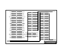
1
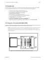
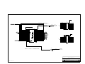
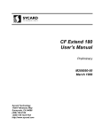
CF extend 160A & CF extend 160B CompactFlash™ Extender Cards User’s Manual Preliminary M200036-03 February 2002 Sycard Technology 1180-F Miraloma Way Sunnyvale, CA 94085 (408) 749-0130 (408) 749-1323 fax http://www.sycard.com CompactFlash™ is a trademark of the CompactFlash Association CF extend 160/160A/160B User’s Manual Page 1 1.0 Introduction Sycard Technology's CF extend 160, CF extend 160A and CF extend 160B CompactFlash extender cards are debug tool for CompactFlash development and test. CF extend 160/160A/160B offers the following features: • • • • • • • • • • • Push button switches simulates card removal/insertion cycle Low profile enclosure compatible with all CompactFlash hosts 4 layer construction to insure low noise environment All 50-pins available as test points Both I/O and memory mode signals clearly marked Vcc can be isolated through jumper blocks for current measurements Surface mount resistors can be added to any signal line Vcc LEDs indicate 3.3V or 5V operation Convenient grounding posts for scope probes or other test equipment Supports type I CompactFlash (3.3mm) cards - CF extend 160 Supports type I and type II CompactFlash (3.3mm and 5.0mm) cards - CF extend 160A/160B 2.0 Using the CF extend 160/160A/160B Using the CF extend 160/160A/160B is relatively straightforward. The extender card is inserted into the desired slot in the host system. Then the CompactFlash card under test is inserted into the card connector. Caution: Insertion and removal of the extender and CF card should be done with care. The CF Card's fragile connectors may be broken or bent if improper force is used. Both card and extender should be inserted straight without any lateral movement or force. Proper care and use of the extender card will insure years of trouble free operation. Vcc JP1 P1 1 -C D 2 D2 D0 A1 A3 A5 VCC A8 -OE CE1D6 D4 GN D JP3 G nd SW 2 J P2 GND GND -IO 1 6 D9 D1 B V D 1 A 0 -R E G A 2 -W A IT A 4 -V S 2 A6 VCC -W E A7 A 9 -IOR D A 1 0 -C E2 D7 D14 D5 D12 D3 -C D 1 SW 1 GND D10 D8 B V D2 -IN P RST -C S E L IR E Q -IO W R -V S 1 D15 D13 D11 P2 G nd PW R +5V JP4 Figure 2.0-1 The CF extend 160, CF extend 160A and CF extend 160B M200036-03 1999-2002 Sycard Technology Page 2 CF extend 160/160A/160B User’s Manual 2.1 Test Points All 68-pins of the interface are available to probe through clearly marked headers. The headers are standard 0.1” dual row headers with 0.025” posts designed to accept a wide variety of test probes and cable assemblies. 2.2 Power Indicators Two LED power indicators display the status of the socket’s Vcc. The PWR LED indicates that power is applied to the board. When both the PWR LED and the 5V LED are lit, a Vcc of greater than approximately 3.5V is present. When only the PWR LED is lit, the Vcc is at a level of less than 3.5V. Note: The power LEDs are designed to indicate the presence of power on the Vcc supply pins. The LEDs do not provide an accurate measurement of Vcc. Use a voltmeter to determine the actual operating voltage. 2.2 Current Measurements The Vcc power bus may be isolated from the CF Card socket through two jumper blocks labeled JP3 and JP4. Both jumpers must be removed to isolate the power. A current meter can be inserted to measure card current consumption. Caution: Care must be taken to insure that the current measuring device is inserted before turning on power to the host socket. Improper power sequencing may cause a damaging latchup condition. 2.3 Using the Card Detect Switches CF extend 160/160A160B includes two micro switches (SW1 and SW2) which can be used to momentarily interrupt the CD1- and CD2- signals. By interrupting the CD1- and CD2- signals, a card removal/insertion cycle can be simulated. To test the operation of the Card Detect switches, be sure that your CF Card Software drivers are loaded. Momentarily press both of the Card Detect switches. Most software drivers will issue a removal beep followed by an insertion beep. The software may also remove power from the socket when the card is removed. 2.4 Termination Area An area with SMT resistors is located between the test points and the card connector allows access to all CF Card signals. A series of surface mount pads allows the user to isolate a signal by cutting a trace. The user may also add series resistors to any signal. When shipped from the factory, the resistor pads are shorted with PCB traces. In order to insert series resistor, these traces must be cut prior to soldering the resistor to the board. Figure 2.4-1 and 2.4-2 illustrate the termination areas located on both sides of the CF extend 160 board. Use this guide when making modifications to the board, since the silk-screen designations may be difficult to read. 1999-2002 Sycard Technology M200036-03 CF extend 160/160A/160B User’s Manual Page 3 SW2 Vcc GND JP3 WP/IO16# R19 R21 CD2A# D1 R34 R35 D2 A0 R6 R33 D0 A2 R3 R20 A1 A3 R23 R22 A3 A6 R1 R24 A5 A7 R2 R26 A7 OE# R4 R28 A9 CE1# R5 R29 A10 D6 R39 R40 D7 D4 R37 R38 D5 R36 D3 SW1 JP4 GND Figure 2.4-1 Termination Area - Component Side D10 R43 R42 D9 D8 R41 R7 BVD1 BVD2 R8 R9 REG# INP# R11 R10 WAIT# RESET R13 R12 VS2# CSEL# R14 R16 RDY/IREQ WE# R15 R18 IOWR# IORD# R17 R30 VS1# CE2# R31 R48 D15 D14 R47 R46 D13 D12 R45 R44 D11 CD1A# R32 Figure 2.4-2 Termination Area - Solder Side M200036-03 1999-2002 Sycard Technology Appendix A A-1 Appendix A A. CompactFlash 50-Pin Interface Pin 1 2 3 4 5 6 7 8 9 10 11 12 13 14 15 16 17 18 19 20 21 22 23 24 25 Name GND D03 D04 D05 D06 D07 CE1# A10 OE# A09 A08 A07 VCC A06 A05 A04 A03 A02 A01 A00 D00 D01 D02 WP/IOIS16 CD2# M200036-03 Description Ground Data Bit 3 Data Bit 4 Data Bit 5 Data Bit 6 Data Bit 7 Card Enable 1 Address Bit 10 Output Enable Address Bit 9 Address Bit 8 Address Bit 7 Card Power Address Bit 6 Address Bit 5 Address Bit 4 Address Bit 3 Address Bit 2 Address Bit 1 Address Bit 0 Data Bit 0 Data Bit 1 Data Bit 2 Write Protect I/O is 16 Bits Card Detect 2 Pin 26 27 28 29 30 31 32 33 34 35 36 37 38 39 40 41 42 43 44 45 46 47 48 49 50 Name CD1# D11 D12 D13 D14 D15 CE2# VS1# IORD# IOWR# WE# RDY/BSY/IREQ VCC CSEL# VS2# RESET WAIT# INPACK# REG# BVD2 BVD1 D08 D09 D10 GND Description Card Detect 1 Data Bit 11 Data Bit 12 Data Bit 13 Data Bit 14 Data Bit 15 Card Enable 2 Voltage Sense 1 I/O Read Strobe I/O Write Strobe Write Enable Ready/Busy/Interrupt Request Card Power Master Slave Select Voltage Sense 2 Card Reset Extend Bus Cycle Input Port Acknowledge Register Select Battery Voltage Detect 2 Battery Voltage Detect 1 Data Bit 8 Data Bit 9 Data Bit 10 Ground 1999-2002 Sycard Technology Appendix B B-1 B. CF extend 160 Schematic M200036-03 1999-2002 Sycard Technology A[0..10] D[0..15] CD2# D2 D0 A1 A3 A5 A[0..10] D[0..15] SW1 CD1A# CD1# CD1A# VCC PUSHBUTTON D3 D4 D5 D6 D7 CE1# OE# CE1# A10 OE# A9 A8 A7 A6 VCC A5 A4 A3 A2 A1 A0 WP/IO16# D0 D1 D2 WP/IO16# 1 2 3 4 5 6 7 8 9 10 11 12 13 14 15 16 17 18 19 20 21 22 23 24 25 P1 GND CD1 D3 D11 D4 D12 D5 D13 D6 D14 D7 D15 CE1 CE2 A10 VS1 OE IORD A9 IOWR A8 WE A7 RDYIREQ VCCX VCCX A6 CSEL A5 VS2 A4 RESET A3 WAIT A2 INPACK A1 REG A0 BVD2 D0 BVD1 D1 D8 D2 D9 WP/IO16 D10 GND CD2 CF CARD 26 27 28 29 30 31 32 33 34 35 36 37 38 39 40 41 42 43 44 45 46 47 48 49 50 D11 D12 D13 D14 D15 CE2# VS1# IORD# IOWR# WE# RDY/IREQ VCC CSEL# VS2# RESET WAIT# INP# REG# BVD2 BVD1 D8 D9 D10 A8 OE# CE1# D6 D4 JP1 1 2 3 4 5 6 7 8 9 10 11 12 13 14 15 16 17 18 19 20 21 22 23 24 25 26 HEADER 13X2 WP/IO16# D1 A0 A2 A4 A6 A7 A9 A10 D7 D5 D3 JP2 1 2 3 4 5 6 7 8 9 10 11 12 13 14 15 16 17 18 19 20 21 22 23 24 25 26 HEADER 13X2 D10 D8 BVD2 INP# RESET CSEL# RDY/IREQ IOWR# VS1# D15 D13 D11 CE2# VS1# IORD# IOWR# WE# RDY/IREQ CSEL# VS2# RESET WAIT# INP# REG# BVD2 BVD1 D9 BVD1 REG# WAIT# VS2# VCC WE# IORD# CE2# D14 D12 CD1# CD2# SW2 CD2A# HOST SIDE CONNECTOR CD2A# PUSHBUTTON Sycard Technology Title FILE=CFEXT1.S31 CFextend 160 - Host Connector Size Document Number B 140015 Date: October 23, 1997 Sheet 1 of REV A 3 R21 CD2A# CD2AR# CD2A# AR[0..10] CD2AR# 0 OHM AR0 R4 OE# OER# OE# CE1R# AR1 CE1R# R3 A2 WP/IO16R# AR2 R22 A3 BVD1R AR3 R23 A4 BVD2R AR4 BVD2R R24 A5 REGR# AR5 REGR# R1 A6 WAITR# AR6 R26 A7 INPR# AR7 R2 A8 VS2R# AR8 VS2R# R28 A9 RESETR AR9 R42 D9 0 OHM RESETR DR9 0 OHM 0 OHM R29 A10 R14 CSEL# DR8 0 OHM R13 CSEL# R41 D8 0 OHM 0 OHM RESET DR7 0 OHM R12 RESET R40 D7 0 OHM INPR# 0 OHM VS2# DR6 0 OHM R11 VS2# R39 D6 0 OHM WAITR# 0 OHM INP# DR5 0 OHM R10 INP# R38 D5 0 OHM 0 OHM WAIT# DR4 0 OHM R9 WAIT# R37 D4 0 OHM 0 OHM REG# DR3 0 OHM R8 REG# R36 D3 0 OHM BVD1R 0 OHM BVD2 DR2 0 OHM R7 BVD2 R35 D2 0 OHM WP/IO16R# 0 OHM BVD1 DR1 0 OHM R19 BVD1 R34 D1 0 OHM 0 OHM WP/IO16# DR0 R20 A1 WP/IO16# D0 0 OHM R5 CE1# R33 0 OHM OER# 0 OHM CE1# AR[0..10] R6 A0 CSELR# AR10 R43 D10 0 OHM CSELR# DR10 0 OHM 0 OHM R44 WER# WE# R30 WER# VS1# 0 OHM VS1# VS1R# 0 OHM VS1R# 0 OHM R45 RDY/IREQ RDY/IREQR R31 RDY/IREQR CE2# 0 OHM CE2# CE2R# 0 OHM CE2R# 0 OHM R46 IORD# IORDR# R32 IORDR# CD1A# 0 OHM CD1A# CD1AR# 0 OHM CD1AR# 0 OHM IOWR# R47 DR14 D14 R18 IOWR# DR13 D13 R17 IORD# DR12 D12 R16 RDY/IREQ DR11 D11 R15 WE# IOWRR# IOWRR# 0 OHM 0 OHM R48 D15 DR15 0 OHM A[0..10] D[0..15] FILE=CFEXT2.S31 A[0..10] D[0..15] DR[0..15] DR[0..15] Sycard Technology Title CFextend 160 - Series Resistors Size Document Number B 140015 Date: November 21, 1997 Sheet 2 of REV A 3 5V LED R25 D2 D1 110 ohm RED LED 3.3V ZENER R27 D3 220 ohm VCC AR[0..10] DR[0..15] AR[0..10] DR[0..15] CD1AR# YEL LED POWER LED JP3 VCC2 DR3 DR4 DR5 DR6 DR7 JUMPER JP4 JUMPER CX1 0.1uF C1 0.1uF C2 0.1uF C3 3.3uF C4 3.3uF CE1R# OER# CX2 0.1uF WP/IO16R# CD2AR# CE1R# AR10 OER# AR9 AR8 AR7 VCC2 AR6 AR5 AR4 AR3 AR2 AR1 AR0 DR0 DR1 DR2 WP/IO16R# CD2AR# 1 2 3 4 5 6 7 8 9 10 11 12 13 14 15 16 17 18 19 20 21 22 23 24 25 P2 GND CD1 D3 D11 D4 D12 D5 D13 D6 D14 D7 D15 CE1 CE2 A10 VS1 OE IORD A9 IOWR A8 WE A7 RDYIREQ VCCX VCCX A6 CSEL A5 VS2 A4 RESET A3 WAIT A2 INPACK A1 REG A0 BVD2 D0 BVD1 D1 D8 D2 D9 WP/IO16 D10 GND CD2 CF HOST 26 27 28 29 30 31 32 33 34 35 36 37 38 39 40 41 42 43 44 45 46 47 48 49 50 DR11 DR12 DR13 DR14 DR15 CE2R# VS1R# IORDR# IOWRR# WER# RDY/IREQR VCC2 CSELR# VS2R# RESETR WAITR# INPR# REGR# BVD2R BVD1R DR8 DR9 DR10 CD1AR# CE2R# VS1R# IORDR# IOWRR# WER# RDY/IREQR CSELR# VS2R# RESETR WAITR# INPR# REGR# BVD2R BVD1R SOCKET SIDE CONNECTOR Sycard Technology Title FILE=CFEXT3.S31 CFextend 160 - Card Side Size Document Number B 140015 Date: November 21, 1997 Sheet 3 of REV A 3