1
Freescale Semiconductor, Inc...
Freescale Semiconductor, Inc.
OVERVIEW
1
SIGNAL DESCRIPTIONS
2
MEMORY, OPERATING MODES, AND INTERRUPTS
3
EXTERNAL MEMORY INTERFACE
4
SERIAL HOST INTERFACE
5
SERIAL AUDIO INTERFACE
6
GENERAL PURPOSE I/O
7
BOOTSTRAP CODE CONTENTS
A
PROGRAMMING REFERENCE
B
APPLICATION EXAMPLES
C
INDEX
I
For More Information On This Product,
Go to: www.freescale.com
Freescale Semiconductor, Inc...
Freescale Semiconductor, Inc.
1
OVERVIEW
2
SIGNAL DESCRIPTIONS
3
MEMORY, OPERATING MODES, AND INTERRUPTS
4
EXTERNAL MEMORY INTERFACE
5
SERIAL HOST INTERFACE
6
SERIAL AUDIO INTERFACE
7
GENERAL PURPOSE I/O
A
BOOTSTRAP CODE CONTENTS
B
PROGRAMMING SHEETS
C
APPLICATION EXAMPLES
I
INDEX
For More Information On This Product,
Go to: www.freescale.com
Freescale Semiconductor, Inc.
Freescale Semiconductor, Inc...
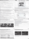
DSP56009
24-Bit Digital Signal Processor
User’s Manual
Motorola, Incorporated
Semiconductor Products Sector
DSP Division
6501 William Cannon Drive West
Austin, TX 78735-8598
For More Information On This Product,
Go to: www.freescale.com
Freescale Semiconductor, Inc.
This document (and other documents) can be viewed on the World Wide
Web at http://www.motorola-dsp.com.
This manual is one of a set of three documents. You need the following
manuals to have complete product information: Family Manual, User’s
Manual, and Technical Data.
Freescale Semiconductor, Inc...
OnCE is a trademark of Motorola, Inc.
MOTOROLA INC., 1996
Order this document by DSP56009UM/AD
Motorola reserves the right to make changes without further notice to any products
herein to improve reliability, function, or design. Motorola does not assume any
liability arising out of the application or use of any product or circuit described
herein; neither does it convey any license under its patent rights nor the rights of
others. Motorola products are not authorized for use as components in life support
devices or systems intended for surgical implant into the body or intended to
support or sustain life. Buyer agrees to notify Motorola of any such intended end use
whereupon Motorola shall determine availability and suitability of its product or
are registered trademarks of
products for the use intended. Motorola and
Motorola, Inc. Motorola, Inc. is an Equal Employment Opportunity /Affirmative
Action Employer.
For More Information On This Product,
Go to: www.freescale.com
Freescale Semiconductor, Inc.
Freescale Semiconductor, Inc...
TABLE OF CONTENTS
SECTION 1
OVERVIEW . . . . . . . . . . . . . . . . . . . . . . . . . . . . . . . 1-1
1.1
INTRODUCTION . . . . . . . . . . . . . . . . . . . . . . . . . . . . . . . . . . . . . .1-3
1.1.1
Manual Organization . . . . . . . . . . . . . . . . . . . . . . . . . . . . . 1-4
1.1.2
Manual Conventions . . . . . . . . . . . . . . . . . . . . . . . . . . . . . 1-5
1.2
DSP56009 FEATURES. . . . . . . . . . . . . . . . . . . . . . . . . . . . . . . .1-6
1.3
DSP56009 ARCHITECTURAL OVERVIEW . . . . . . . . . . . . . .1-8
1.3.1
Memory and Peripheral Modules. . . . . . . . . . . . . . . . . . . 1-10
1.3.2
DSP Core Processor . . . . . . . . . . . . . . . . . . . . . . . . . . . . 1-10
1.3.2.1
Data Arithmetic and Logic Unit (ALU) . . . . . . . . . . . . . 1-11
1.3.2.2
Address Generation Unit (AGU) . . . . . . . . . . . . . . . . . 1-11
1.3.2.3
Program Control Unit . . . . . . . . . . . . . . . . . . . . . . . . . 1-12
1.3.2.4
Data Buses . . . . . . . . . . . . . . . . . . . . . . . . . . . . . . . . . 1-12
1.3.2.5
Address Buses . . . . . . . . . . . . . . . . . . . . . . . . . . . . . . 1-12
1.3.2.6
Phase Lock Loop (PLL). . . . . . . . . . . . . . . . . . . . . . . . 1-12
1.3.2.7
On-Chip Emulation (OnCE) Port . . . . . . . . . . . . . . . . . 1-13
1.3.3
Memories . . . . . . . . . . . . . . . . . . . . . . . . . . . . . . . . . . . . . 1-13
1.3.3.1
Program Memory . . . . . . . . . . . . . . . . . . . . . . . . . . . . 1-13
1.3.3.2
X Data Memory . . . . . . . . . . . . . . . . . . . . . . . . . . . . . . 1-15
1.3.3.3
Y Data Memory . . . . . . . . . . . . . . . . . . . . . . . . . . . . . . 1-15
1.3.3.4
On-Chip Memory Configuration Bits . . . . . . . . . . . . . . 1-15
1.3.3.5
Bootstrap ROM . . . . . . . . . . . . . . . . . . . . . . . . . . . . . . 1-15
1.3.3.6
External Memory . . . . . . . . . . . . . . . . . . . . . . . . . . . . . 1-16
1.3.3.7
Reserved Memory Spaces . . . . . . . . . . . . . . . . . . . . . 1-16
1.3.4
Input/Output . . . . . . . . . . . . . . . . . . . . . . . . . . . . . . . . . . . 1-16
1.3.4.1
External Memory Interface . . . . . . . . . . . . . . . . . . . . . 1-18
1.3.4.2
Serial Host Interface (SHI) . . . . . . . . . . . . . . . . . . . . . 1-18
1.3.4.3
Serial Audio Interface (SAI). . . . . . . . . . . . . . . . . . . . . 1-19
1.3.4.4
General Purpose Input/Output . . . . . . . . . . . . . . . . . . 1-19
MOTOROLA
DSP56009 User’s Manual
For More Information On This Product,
Go to: www.freescale.com
iii
Freescale Semiconductor, Inc...
Freescale Semiconductor, Inc.
SECTION 2
SIGNAL DESCRIPTIONS . . . . . . . . . . . . . . . . . . . . 2-1
2.1
SIGNAL GROUPINGS . . . . . . . . . . . . . . . . . . . . . . . . . . . . . . . . 2-3
2.2
POWER . . . . . . . . . . . . . . . . . . . . . . . . . . . . . . . . . . . . . . . . . . . . . 2-5
2.3
GROUND. . . . . . . . . . . . . . . . . . . . . . . . . . . . . . . . . . . . . . . . . . . . 2-5
2.4
CLOCK AND PLL SIGNALS . . . . . . . . . . . . . . . . . . . . . . . . . . . 2-6
2.5
EXTERNAL MEMORY INTERFACE (EMI) . . . . . . . . . . . . . . . 2-7
2.6
INTERRUPT AND MODE CONTROL . . . . . . . . . . . . . . . . . . . 2-10
2.7
SERIAL HOST INTERFACE (SHI). . . . . . . . . . . . . . . . . . . . . 2-14
2.8
SERIAL AUDIO INTERFACE (SAI) . . . . . . . . . . . . . . . . . . . 2-18
2.8.1
SAI Receiver Section . . . . . . . . . . . . . . . . . . . . . . . . . . . 2-18
2.8.2
SAI Transmitter Section . . . . . . . . . . . . . . . . . . . . . . . . . 2-20
2.9
GENERAL PURPOSE I/O . . . . . . . . . . . . . . . . . . . . . . . . . . . . 2-21
2.10
ON-CHIP EMULATION (ONCE TM) PORT . . . . . . . . . . . . . . 2-22
SECTION
3.1
3.2
3.2.1
3.2.2
3.2.3
3.2.4
3.2.5
3.3
3.3.1
3.3.2
3.4
3.4.1
3.4.2
3.4.3
3.4.4
3.5
3.6
3.7
3.8
iv
3
MEMORY, OPERATING MODES,
AND INTERRUPTS . . . . . . . . . . . . . . . . . . . . . . . . . 3-1
INTRODUCTION . . . . . . . . . . . . . . . . . . . . . . . . . . . . . . . . . . . . . 3-3
DSP56009 DATA AND PROGRAM MEMORY . . . . . . . . . . . 3-3
X Data ROM . . . . . . . . . . . . . . . . . . . . . . . . . . . . . . . . . . . 3-4
Y Data ROM . . . . . . . . . . . . . . . . . . . . . . . . . . . . . . . . . . . 3-4
Program ROM . . . . . . . . . . . . . . . . . . . . . . . . . . . . . . . . . . 3-4
Bootstrap ROM . . . . . . . . . . . . . . . . . . . . . . . . . . . . . . . . . 3-4
Reserved Memory Spaces . . . . . . . . . . . . . . . . . . . . . . . . 3-5
DSP56009 DATA AND PROGRAM MEMORY MAPS. . . . . 3-5
Dynamic Switching of Memory Configurations . . . . . . . . . 3-8
Internal I/O Memory Map . . . . . . . . . . . . . . . . . . . . . . . . . 3-9
OPERATING MODE REGISTER (OMR) . . . . . . . . . . . . . . . . 3-11
DSP Operating Mode (MC, MB, MA)—Bits 4, 1, and 0. . 3-11
Program RAM Enable A (PEA)—Bit 2 . . . . . . . . . . . . . . 3-11
Program RAM Enable B (PEB)—Bit 3 . . . . . . . . . . . . . . 3-12
Stop Delay (SD)—Bit 6 . . . . . . . . . . . . . . . . . . . . . . . . . . 3-12
OPERATING MODES . . . . . . . . . . . . . . . . . . . . . . . . . . . . . . . . 3-12
INTERRUPT PRIORITY REGISTER . . . . . . . . . . . . . . . . . . . 3-14
PHASE LOCK LOOP (PLL) CONFIGURATION . . . . . . . . . . 3-18
HARDWARE RESET OPERATION . . . . . . . . . . . . . . . . . . . . 3-19
DSP56009 User’s Manual
For More Information On This Product,
Go to: www.freescale.com
MOTOROLA
Freescale Semiconductor, Inc...
Freescale Semiconductor, Inc.
SECTION 4
EXTERNAL MEMORY INTERFACE . . . . . . . . . . . . 4-1
4.1
INTRODUCTION . . . . . . . . . . . . . . . . . . . . . . . . . . . . . . . . . . . . . .4-3
4.1.1
Theory of Operation. . . . . . . . . . . . . . . . . . . . . . . . . . . . . . 4-3
4.1.2
EMI Features . . . . . . . . . . . . . . . . . . . . . . . . . . . . . . . . . . . 4-4
4.2
EMI PROGRAMMING MODEL. . . . . . . . . . . . . . . . . . . . . . . . . . .4-5
4.2.1
EMI Base Address Registers (EBAR0 and EBAR1) . . . . . 4-7
4.2.2
EMI Write Offset Register (EWOR) . . . . . . . . . . . . . . . . . . 4-7
4.2.3
EMI Offset Register (EOR) . . . . . . . . . . . . . . . . . . . . . . . . 4-8
4.2.4
EMI Data Write Registers (EDWR) . . . . . . . . . . . . . . . . . . 4-9
4.2.5
EMI Data Read Register (EDRR) . . . . . . . . . . . . . . . . . . . 4-9
4.2.6
EMI Data Register Buffer (EDRB) . . . . . . . . . . . . . . . . . . . 4-9
4.2.7
EMI Control/Status Register (ECSR) . . . . . . . . . . . . . . . . 4-10
4.2.7.1
EMI Data Bus Width (EBW)—Bit 0 . . . . . . . . . . . . . . . 4-10
4.2.7.2
EMI Word Length (EWL[2:0])—Bits 16,2, and 1 . . . . . 4-11
4.2.7.3
EMI Addressing Mode (EAM[3:0])—Bits 6–3 . . . . . . . 4-12
4.2.7.4
EMI Increment EBAR After Read (EINR)—Bit 7 . . . . . 4-16
4.2.7.5
EMI Increment EBAR After Write (EINW)—Bit 8 . . . . 4-16
4.2.7.6
EMI Interrupt Select (EIS[1:0])—Bits 9–10 . . . . . . . . . 4-17
4.2.7.7
EMI Memory-Wrap Interrupt Enable
(EMWIE)—Bit 11. . . . . . . . . . . . . . . . . . . . . . . . . . . . . 4-17
4.2.7.8
EMI Data Write Register Empty (EDWE)—Bit 12 . . . . 4-18
4.2.7.9
EMI Data Read Register Full (EDRF)—Bit 13 . . . . . . 4-18
4.2.7.10
EMI Data Register Buffer and Data Read Register
Full (EBDF)—Bit 14. . . . . . . . . . . . . . . . . . . . . . . . . . . 4-18
4.2.7.11
EMI Busy (EBSY)—Bit 15 . . . . . . . . . . . . . . . . . . . . . . 4-19
4.2.7.12
EMI Read Trigger Select (ERTS)—Bit 17 . . . . . . . . . . 4-19
4.2.7.13
EMI DRAM Memory Timing (EDTM)—Bit 18 . . . . . . . 4-19
4.2.7.14
EMI SRAM Memory Timing
(ESTM[3:0])— Bits 19–22 . . . . . . . . . . . . . . . . . . . . . . 4-20
4.2.7.15
EMI Enable (EME)—Bit 23 . . . . . . . . . . . . . . . . . . . . . 4-21
4.2.8
EMI Refresh Control Register (ERCR) . . . . . . . . . . . . . . 4-21
4.2.8.1
EMI Refresh Clock Divider (ECD[7:0])—Bits 0–7 . . . . 4-22
4.2.8.2
ERCR Reserved Bits—Bits 8–17, 21 . . . . . . . . . . . . . 4-22
4.2.8.3
EMI Refresh Clock Prescaler
(EPS[1:0])—Bits 18–19 . . . . . . . . . . . . . . . . . . . . . . . . 4-22
4.2.8.4
EMI One-Shot Refresh (EOSR)—Bit 20 . . . . . . . . . . . 4-22
MOTOROLA
DSP56009 User’s Manual
For More Information On This Product,
Go to: www.freescale.com
v
Freescale Semiconductor, Inc.
Freescale Semiconductor, Inc...
4.2.8.5
4.2.8.6
4.3
4.3.1
4.3.2
4.3.3
4.3.4
4.4
4.4.1
4.4.2
4.4.3
4.4.3.1
4.4.3.2
4.4.4
4.4.5
4.5
4.5.1
4.5.2
4.5.3
4.5.4
4.5.5
4.6
4.7
4.8
4.8.1
4.8.1.1
4.8.1.2
4.8.2
EMI Refresh Enable when Debugging (ERED)—Bit 22 . . .
4-22
ERCR Refresh Enable (EREF)—Bit 23 . . . . . . . . . . . 4-23
EMI ADDRESS GENERATION . . . . . . . . . . . . . . . . . . . . . . . . 4-23
SRAM Absolute Addressing . . . . . . . . . . . . . . . . . . . . . . 4-24
SRAM Relative Addressing. . . . . . . . . . . . . . . . . . . . . . . 4-25
DRAM Relative Addressing. . . . . . . . . . . . . . . . . . . . . . . 4-27
DRAM Absolute Addressing . . . . . . . . . . . . . . . . . . . . . . 4-30
DRAM REFRESH . . . . . . . . . . . . . . . . . . . . . . . . . . . . . . . . . . . . 4-31
DRAM Refresh Without Using The Internal Refresh
Timer . . . . . . . . . . . . . . . . . . . . . . . . . . . . . . . . . . . . . . . . 4-31
DRAM Refresh OnCE‰ Port Debug Mode
Consideration . . . . . . . . . . . . . . . . . . . . . . . . . . . . . . . . . 4-32
Using The Internal Refresh Timer . . . . . . . . . . . . . . . . . . 4-33
“On Line” Refresh . . . . . . . . . . . . . . . . . . . . . . . . . . . . 4-33
“Off Line” Refresh . . . . . . . . . . . . . . . . . . . . . . . . . . . . 4-34
Software Controlled Refresh . . . . . . . . . . . . . . . . . . . . . . 4-34
DRAM Refresh Timing . . . . . . . . . . . . . . . . . . . . . . . . . . 4-35
EMI OPERATING CONSIDERATIONS . . . . . . . . . . . . . . . . . 4-38
EMI Triggering and Pipelining . . . . . . . . . . . . . . . . . . . . . 4-38
Read Data Transfer. . . . . . . . . . . . . . . . . . . . . . . . . . . . . 4-40
Write-Data Transfer. . . . . . . . . . . . . . . . . . . . . . . . . . . . . 4-43
EMI Operation During Stop . . . . . . . . . . . . . . . . . . . . . . . 4-45
EMI Operation During Wait . . . . . . . . . . . . . . . . . . . . . . . 4-45
DATA-DELAY STRUCTURE . . . . . . . . . . . . . . . . . . . . . . . . . 4-46
EMI-TO-MEMORY CONNECTION . . . . . . . . . . . . . . . . . . . . . 4-48
EMI TIMING . . . . . . . . . . . . . . . . . . . . . . . . . . . . . . . . . . . . . . . . 4-50
Timing Diagrams for DRAM Addressing Modes . . . . . . . 4-51
Fast Timing Mode. . . . . . . . . . . . . . . . . . . . . . . . . . . . 4-52
Slow Timing Mode . . . . . . . . . . . . . . . . . . . . . . . . . . . 4-58
Timing Diagrams for SRAM Addressing Modes . . . . . . . 4-64
SECTION 5
SERIAL HOST INTERFACE . . . . . . . . . . . . . . . . . . 5-1
5.1
INTRODUCTION . . . . . . . . . . . . . . . . . . . . . . . . . . . . . . . . . . . . . 5-3
5.2
SERIAL HOST INTERFACE INTERNAL ARCHITECTURE. 5-4
5.2.1
SHI Clock Generator . . . . . . . . . . . . . . . . . . . . . . . . . . . . . 5-5
vi
DSP56009 User’s Manual
For More Information On This Product,
Go to: www.freescale.com
MOTOROLA
Freescale Semiconductor, Inc...
Freescale Semiconductor, Inc.
5.3
SERIAL HOST INTERFACE PROGRAMMING MODEL . . . . .5-5
5.3.1
SHI Input/Output Shift Register (IOSR)—Host Side . . . . . 5-8
5.3.2
SHI Host Transmit Data Register (HTX)—DSP Side. . . . . 5-8
5.3.3
SHI Host Receive Data FIFO (HRX)—DSP Side . . . . . . . 5-9
5.3.4
SHI Slave Address Register (HSAR)—DSP Side . . . . . . . 5-9
5.3.4.1
HSAR Reserved Bits—Bits 17–0,19 . . . . . . . . . . . . . . . 5-9
5.3.4.2
HSAR I2C Slave Address
(HA[6:3], HA1)—Bits 23–20,18 . . . . . . . . . . . . . . . . . . . 5-9
5.3.5
SHI Clock Control Register (HCKR)—DSP Side . . . . . . . . 5-9
5.3.5.1
Clock Phase and Polarity
(CPHA and CPOL)—Bits 1–0 . . . . . . . . . . . . . . . . . . . 5-10
5.3.5.2
HCKR Prescaler Rate Select (HRS)—Bit 2 . . . . . . . . 5-11
5.3.5.3
HCKR Divider Modulus Select
(HDM[5:0])—Bits 8–3 . . . . . . . . . . . . . . . . . . . . . . . . . 5-12
5.3.5.4
HCKR Reserved Bits—Bits 23–14, 11–9 . . . . . . . . . . 5-12
5.3.5.5
HCKR Filter Mode (HFM[1:0]) — Bits 13–12 . . . . . . . 5-12
5.3.6
SHI Control/Status Register (HCSR)—DSP Side . . . . . . 5-13
5.3.6.1
HCSR Host Enable (HEN)—Bit 0 . . . . . . . . . . . . . . . . 5-13
5.3.6.2
HCSR I2C/SPI Selection (HI2C)—Bit 1. . . . . . . . . . . . 5-13
5.3.6.3
HCSR Serial Host Interface Mode
(HM[1:0])—Bits 3–2. . . . . . . . . . . . . . . . . . . . . . . . . . . 5-14
5.3.6.4
HCSR Reserved Bits—Bits 23, 18, 16, and 4 . . . . . . . 5-14
5.3.6.5
HCSR FIFO-Enable Control (HFIFO)—Bit 5. . . . . . . . 5-14
5.3.6.6
HCSR Master Mode (HMST)—Bit 6 . . . . . . . . . . . . . . 5-14
5.3.6.7
HCSR Host-Request Enable
(HRQE[1:0])—Bits 8–7 . . . . . . . . . . . . . . . . . . . . . . . . 5-15
5.3.6.8
HCSR Idle (HIDLE)—Bit 9 . . . . . . . . . . . . . . . . . . . . . 5-15
5.3.6.9
HCSR Bus-Error Interrupt Enable (HBIE)—Bit 10 . . . 5-16
5.3.6.10
HCSR Transmit-Interrupt Enable (HTIE)—Bit 11 . . . . 5-16
5.3.6.11
HCSR Receive Interrupt Enable
(HRIE[1:0])—Bits 13–12 . . . . . . . . . . . . . . . . . . . . . . . 5-16
5.3.6.12
HCSR Host Transmit Underrun Error
(HTUE)—Bit 14 . . . . . . . . . . . . . . . . . . . . . . . . . . . . . . 5-17
5.3.6.13
HCSR Host Transmit Data Empty (HTDE)—Bit 15. . . 5-17
5.3.6.14
Host Receive FIFO Not Empty (HRNE)—Bit 17 . . . . . 5-18
5.3.6.15
Host Receive FIFO Full (HRFF)—Bit 19 . . . . . . . . . . . 5-18
MOTOROLA
DSP56009 User’s Manual
For More Information On This Product,
Go to: www.freescale.com
vii
Freescale Semiconductor, Inc...
Freescale Semiconductor, Inc.
5.3.6.16
Host Receive Overrun Error (HROE)—Bit 20 . . . . . . 5-18
5.3.6.17
Host Bus Error (HBER)—Bit 21 . . . . . . . . . . . . . . . . . 5-18
5.3.6.18
HCSR Host Busy (HBUSY)—Bit 22 . . . . . . . . . . . . . . 5-19
5.4
CHARACTERISTICS OF THE SPI BUS . . . . . . . . . . . . . . . . 5-19
5.4.1
Overview . . . . . . . . . . . . . . . . . . . . . . . . . . . . . . . . . . . . . 5-19
5.5
CHARACTERISTICS OF THE I2C BUS . . . . . . . . . . . . . . . . . 5-20
5.5.1
Overview . . . . . . . . . . . . . . . . . . . . . . . . . . . . . . . . . . . . . 5-20
5.5.2
I2C Data Transfer Formats . . . . . . . . . . . . . . . . . . . . . . . 5-22
5.6
SHI PROGRAMMING CONSIDERATIONS. . . . . . . . . . . . . . 5-23
5.6.1
SPI Slave Mode . . . . . . . . . . . . . . . . . . . . . . . . . . . . . . . 5-24
5.6.2
SPI Master Mode . . . . . . . . . . . . . . . . . . . . . . . . . . . . . . 5-25
5.6.3
I2C Slave Mode . . . . . . . . . . . . . . . . . . . . . . . . . . . . . . . . 5-26
5.6.3.1
Receive Data in I2C Slave Mode . . . . . . . . . . . . . . . . 5-26
5.6.3.2
Transmit Data In I2C Slave Mode. . . . . . . . . . . . . . . . 5-27
5.6.4
I2C Master Mode . . . . . . . . . . . . . . . . . . . . . . . . . . . . . . . 5-28
5.6.4.1
Receive Data in I2C Master Mode . . . . . . . . . . . . . . . 5-29
5.6.4.2
Transmit Data In I2C Master Mode. . . . . . . . . . . . . . . 5-30
5.6.5
SHI Operation During Stop . . . . . . . . . . . . . . . . . . . . . . . 5-31
SECTION 6
SERIAL AUDIO INTERFACE . . . . . . . . . . . . . . . . . 6-1
6.1
INTRODUCTION . . . . . . . . . . . . . . . . . . . . . . . . . . . . . . . . . . . . . 6-3
6.2
SERIAL AUDIO INTERFACE INTERNAL ARCHITECTURE 6-4
6.2.1
Baud-Rate Generator . . . . . . . . . . . . . . . . . . . . . . . . . . . . 6-4
6.2.2
Receive Section Overview . . . . . . . . . . . . . . . . . . . . . . . . 6-5
6.2.3
SAI Transmit Section Overview . . . . . . . . . . . . . . . . . . . . 6-6
6.3
SERIAL AUDIO INTERFACE PROGRAMMING MODEL . . . 6-8
6.3.1
Baud Rate Control Register (BRC) . . . . . . . . . . . . . . . . . . 6-9
6.3.1.1
Prescale Modulus select (PM[7:0])—Bits 7–0 . . . . . . 6-10
6.3.1.2
Prescaler Range (PSR)—Bit 8 . . . . . . . . . . . . . . . . . . 6-10
6.3.1.3
BRC Reserved Bits—Bits 15–9 . . . . . . . . . . . . . . . . . 6-10
6.3.2
Receiver Control/Status Register (RCS). . . . . . . . . . . . . 6-10
6.3.2.1
RCS Receiver 0 Enable (R0EN)—Bit 0 . . . . . . . . . . . 6-10
6.3.2.2
RCS Receiver 1 Enable (R1EN)—Bit 1 . . . . . . . . . . . 6-11
6.3.2.3
RCS Reserved Bit—Bits 13 and 2 . . . . . . . . . . . . . . . 6-11
6.3.2.4
RCS Receiver Master (RMST)—Bit 3 . . . . . . . . . . . . 6-11
viii
DSP56009 User’s Manual
For More Information On This Product,
Go to: www.freescale.com
MOTOROLA
Freescale Semiconductor, Inc.
Freescale Semiconductor, Inc...
6.3.2.5
RCS Receiver Word Length Control
(RWL[1:0])—Bits 4 and 5 . . . . . . . . . . . . . . . . . . . . . . 6-11
6.3.2.6
RCS Receiver Data Shift Direction (RDIR)—Bit 6 . . . 6-12
6.3.2.7
RCS Receiver Left Right Selection (RLRS)—Bit 7 . . . 6-12
6.3.2.8
RCS Receiver Clock Polarity (RCKP)—Bit 8 . . . . . . . 6-13
6.3.2.9
RCS Receiver Relative Timing (RREL)—Bit 9 . . . . . . 6-13
6.3.2.10
RCS Receiver Data Word Truncation
(RDWT)—Bit 10 . . . . . . . . . . . . . . . . . . . . . . . . . . . . . 6-14
6.3.2.11
RCS Receiver Interrupt Enable (RXIE)—Bit 11 . . . . . 6-15
6.3.2.12
RCS Receiver Interrupt Location (RXIL)—Bit 12 . . . . 6-15
6.3.2.13
RCS Receiver Left Data Full (RLDF)—Bit 14 . . . . . . . 6-16
6.3.2.14
RCS Receiver Right Data Full (RRDF)—Bit 15 . . . . . 6-16
6.3.3
SAI Receive Data Registers (RX0 and RX1). . . . . . . . . . 6-17
6.3.4
Transmitter Control/Status Register (TCS) . . . . . . . . . . . 6-17
6.3.4.1
TCS Transmitter 0 Enable (T0EN)—Bit 0 . . . . . . . . . . 6-17
6.3.4.2
TCS Transmitter 1 Enable (T1EN)—Bit 1 . . . . . . . . . . 6-17
6.3.4.3
TCS Transmitter 2 Enable (T2EN)—Bit 2 . . . . . . . . . . 6-18
6.3.4.4
TCS Transmitter Master (TMST)—Bit 3 . . . . . . . . . . . 6-18
6.3.4.5
TCS Transmitter Word Length Control
(TWL[1:0])—Bits 4 & 5 . . . . . . . . . . . . . . . . . . . . . . . . 6-18
6.3.4.6
TCS Transmitter Data Shift Direction (TDIR)—Bit 6 . . 6-18
6.3.4.7
TCS Transmitter Left Right Selection (TLRS)—Bit 7 . 6-19
6.3.4.8
TCS Transmitter Clock Polarity (TCKP)—Bit 8 . . . . . . 6-19
6.3.4.9
TCS Transmitter Relative Timing (TREL)—Bit 9. . . . . 6-20
6.3.4.10
TCS Transmitter Data Word Expansion
(TDWE)—Bit 10 . . . . . . . . . . . . . . . . . . . . . . . . . . . . . 6-20
6.3.4.11
TCS Transmitter Interrupt Enable (TXIE)—Bit 11 . . . . 6-21
6.3.4.12
TCS Transmitter Interrupt Location (TXIL)—Bit 12 . . . 6-22
6.3.4.13
TCS Reserved Bit—Bit 13. . . . . . . . . . . . . . . . . . . . . . 6-22
6.3.4.14
TCS Transmitter Left Data Empty (TLDE)—Bit 14 . . . 6-22
6.3.4.15
TCS Transmitter Right Data Empty (TRDE)—Bit 15. . 6-23
6.3.5
SAI Transmit Data Registers (TX2, TX1 and TX0) . . . . . 6-23
6.4
PROGRAMMING CONSIDERATIONS . . . . . . . . . . . . . . . . . 6-24
6.4.1
SAI Operation During Stop . . . . . . . . . . . . . . . . . . . . . . . 6-24
6.4.2
Initiating a Transmit Session . . . . . . . . . . . . . . . . . . . . . . 6-24
MOTOROLA
DSP56009 User’s Manual
For More Information On This Product,
Go to: www.freescale.com
ix
Freescale Semiconductor, Inc.
6.4.3
Freescale Semiconductor, Inc...
6.4.4
Using a Single Interrupt to Service Both Receiver
and Transmitter Sections . . . . . . . . . . . . . . . . . . . . . . . . 6-24
SAI State Machine . . . . . . . . . . . . . . . . . . . . . . . . . . . . . 6-25
SECTION 7
GENERAL PURPOSE INPUT/OUTPUT . . . . . . . . . 7-1
7.1
INTRODUCTION . . . . . . . . . . . . . . . . . . . . . . . . . . . . . . . . . . . . . 7-3
7.2
GPIO PROGRAMMING MODEL . . . . . . . . . . . . . . . . . . . . . . . . 7-3
7.3
GPIO REGISTER (GPIOR) . . . . . . . . . . . . . . . . . . . . . . . . . . . . 7-3
7.3.1
GPIOR Data Bits (GD[3:0])—Bits 3–0. . . . . . . . . . . . . . . . 7-4
7.3.2
GPIOR Reserved Bits—Bits 4–7, 12–15, and 20–23 . . . . 7-4
7.3.3
GPIOR Data Direction Bits (GDD[3:0])—Bits 11–8. . . . . . 7-4
7.3.4
GPIOR Control Bits (GC[3:0])—Bits 19–16. . . . . . . . . . . . 7-4
APPENDIX A BOOTSTRAP ROM CONTENTS . . . . . . . . . . . . . . A-1
A.1
INTRODUCTION . . . . . . . . . . . . . . . . . . . . . . . . . . . . . . . . . . . . . A-3
A.2
BOOTSTRAPPING THE DSP . . . . . . . . . . . . . . . . . . . . . . . . . . A-3
A.3
BOOTSTRAP PROGRAM LISTING. . . . . . . . . . . . . . . . . . . . . A-4
A.4
BOOTSTRAP FLOW CHART . . . . . . . . . . . . . . . . . . . . . . . . . . A-7
APPENDIX B PROGRAMMING REFERENCE . . . . . . . . . . . . . . . B-1
B.1
INTRODUCTION . . . . . . . . . . . . . . . . . . . . . . . . . . . . . . . . . . . . . B-3
B.2
PERIPHERAL ADDRESSES . . . . . . . . . . . . . . . . . . . . . . . . . . . B-3
B.3
INTERRUPT ADDRESSES . . . . . . . . . . . . . . . . . . . . . . . . . . . . B-3
B.4
INTERRUPT PRIORITIES. . . . . . . . . . . . . . . . . . . . . . . . . . . . . B-3
B.5
INSTRUCTION SET SUMMARY . . . . . . . . . . . . . . . . . . . . . . . B-3
B.6
PROGRAMMING SHEETS . . . . . . . . . . . . . . . . . . . . . . . . . . . . . B-3
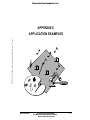
APPENDIX C APPLICATION EXAMPLES . . . . . . . . . . . . . . . . . . C-1
C.1
INTRODUCTION . . . . . . . . . . . . . . . . . . . . . . . . . . . . . . . . . . . . . C-3
C.2
TYPICAL SYSTEM TOPOLOGY . . . . . . . . . . . . . . . . . . . . . . . . C-3
C.3
TYPICAL AUDIO APPLICATION . . . . . . . . . . . . . . . . . . . . . . C-4
C.4
PROGRAM OVERLAY . . . . . . . . . . . . . . . . . . . . . . . . . . . . . . . . C-5
C.5
SINGLE DELAY LINE . . . . . . . . . . . . . . . . . . . . . . . . . . . . . . . . . C-5
C.6
EARLY REFLECTION FILTER . . . . . . . . . . . . . . . . . . . . . . . . . C-6
C.7
TWO CHANNEL COMB FILTER . . . . . . . . . . . . . . . . . . . . . . . . C-7
C.8
3-TAP FIR FILTER . . . . . . . . . . . . . . . . . . . . . . . . . . . . . . . . . C-10
x
DSP56009 User’s Manual
For More Information On This Product,
Go to: www.freescale.com
MOTOROLA
Freescale Semiconductor, Inc.
Freescale Semiconductor, Inc...
LIST OF FIGURES
Figure 1-1
DSP56009 Block Diagram. . . . . . . . . . . . . . . . . . . . . . . . . . . . . . 1-9
Figure 2-1
DSP56009 SIgnals . . . . . . . . . . . . . . . . . . . . . . . . . . . . . . . . . . . 2-4
Figure 3-1
Memory Maps for PEA = 0, PEB = 0 . . . . . . . . . . . . . . . . . . . . . . 3-6
Figure 3-2
Memory Maps for PEA = 1, PEB = 0 . . . . . . . . . . . . . . . . . . . . . . 3-6
Figure 3-3
Memory Maps for PEA = 0, PEB = 1 . . . . . . . . . . . . . . . . . . . . . . 3-7
Figure 3-4
Memory Maps for PEA = 1, PEB = 1 . . . . . . . . . . . . . . . . . . . . . . 3-7
Figure 3-5
Operating Mode Register (OMR). . . . . . . . . . . . . . . . . . . . . . . . 3-11
Figure 3-6
Interrupt Priority Register (Address X:$FFFF). . . . . . . . . . . . . . 3-14
Figure 3-7
PLL Configuration . . . . . . . . . . . . . . . . . . . . . . . . . . . . . . . . . . . 3-18
Figure 4-1
EMI Registers . . . . . . . . . . . . . . . . . . . . . . . . . . . . . . . . . . . . . . . 4-6
Figure 4-2
EMI Control/Status Register (ECSR). . . . . . . . . . . . . . . . . . . . . . 4-8
Figure 4-3
EMI Refresh Control Register (ERCR) . . . . . . . . . . . . . . . . . . . 4-21
Figure 4-4
EMI Address Generation Block Diagram. . . . . . . . . . . . . . . . . . 4-23
Figure 4-5
Refresh Timer Functional Diagram.. . . . . . . . . . . . . . . . . . . . . . 4-33
Figure 4-6
Timing Diagram of a DRAM Refresh Cycle (Fast). . . . . . . . . . . 4-37
Figure 4-7
Timing Diagram Of a DRAM Refresh Cycle (Slow) . . . . . . . . . . 4-37
Figure 4-8
EMI Pipeline . . . . . . . . . . . . . . . . . . . . . . . . . . . . . . . . . . . . . . . 4-39
Figure 4-9
Illustration of the Data-Delay Structure . . . . . . . . . . . . . . . . . . . 4-46
Figure 4-10
DRAM for Data Delay Buffers and for SRAM for Bootstrap . . . 4-48
Figure 4-11
SRAM for Data Delay Buffers and for Bootstrap . . . . . . . . . . . . 4-49
MOTOROLA
DSP56009 User’s Manual
For More Information On This Product,
Go to: www.freescale.com
xi
Freescale Semiconductor, Inc...
Freescale Semiconductor, Inc.
Figure 4-12
Replacing DRAMs with SRAMs for Large Arrays. . . . . . . . . . . . 4-50
Figure 4-13
Fast Read or Write DRAM Access Timing—1 . . . . . . . . . . . . . . 4-52
Figure 4-14
Fast Read or Write DRAM Access Timing—2 . . . . . . . . . . . . . . 4-53
Figure 4-15
Fast Read or Write DRAM Access Timing—3 . . . . . . . . . . . . . . 4-54
Figure 4-16
Fast Read or Write DRAM Access Timing—4 . . . . . . . . . . . . . . 4-55
Figure 4-17
Fast Read or Write DRAM Access Timing—5 . . . . . . . . . . . . . . 4-56
Figure 4-18
Fast Read or Write DRAM Access Timing—6 . . . . . . . . . . . . . . 4-57
Figure 4-19
Slow Read or Write DRAM Access Timing—1. . . . . . . . . . . . . . 4-58
Figure 4-20
Slow Read or Write DRAM Access Timing—2. . . . . . . . . . . . . . 4-59
Figure 4-21
Slow Read or Write DRAM Access Timing—3. . . . . . . . . . . . . . 4-60
Figure 4-22
Slow Read or Write DRAM Access Timing—4. . . . . . . . . . . . . . 4-61
Figure 4-23
Slow Read or Write DRAM Access Timing—5. . . . . . . . . . . . . . 4-62
Figure 4-24
Slow Read or Write DRAM Access Timing—6. . . . . . . . . . . . . . 4-63
Figure 4-25
SRAM Read/Write Timing . . . . . . . . . . . . . . . . . . . . . . . . . . . . . 4-64
Figure 5-1
Serial Host Interface Block Diagram . . . . . . . . . . . . . . . . . . . . . . 5-4
Figure 5-2
SHI Clock Generator . . . . . . . . . . . . . . . . . . . . . . . . . . . . . . . . . . 5-5
Figure 5-3
SHI Programming Model—Host Side. . . . . . . . . . . . . . . . . . . . . . 5-5
Figure 5-4
SHI Programming Model—DSP Side. . . . . . . . . . . . . . . . . . . . . . 5-6
Figure 5-5
SHI I/O Shift Register (IOSR). . . . . . . . . . . . . . . . . . . . . . . . . . . . 5-8
Figure 5-6
SPI Data-To-Clock Timing Diagram . . . . . . . . . . . . . . . . . . . . . . 5-10
Figure 5-7
I2C Bit Transfer. . . . . . . . . . . . . . . . . . . . . . . . . . . . . . . . . . . . . . 5-20
Figure 5-8
I2C Start and Stop Events . . . . . . . . . . . . . . . . . . . . . . . . . . . . . 5-21
xii
DSP56009 User’s Manual
For More Information On This Product,
Go to: www.freescale.com
MOTOROLA
Freescale Semiconductor, Inc...
Freescale Semiconductor, Inc.
Figure 5-9
Acknowledgment on the I2C Bus. . . . . . . . . . . . . . . . . . . . . . . . 5-22
Figure 5-10
I2C Bus Protocol For Host Write Cycle . . . . . . . . . . . . . . . . . . . 5-23
Figure 5-11
I2C Bus Protocol For Host Read Cycle . . . . . . . . . . . . . . . . . . . 5-23
Figure 6-1
SAI Baud-Rate Generator Block Diagram . . . . . . . . . . . . . . . . . . 6-4
Figure 6-2
SAI Receive Section Block Diagram . . . . . . . . . . . . . . . . . . . . . . 6-5
Figure 6-3
SAI Transmit Section Block Diagram . . . . . . . . . . . . . . . . . . . . . 6-7
Figure 6-4
SAI Registers. . . . . . . . . . . . . . . . . . . . . . . . . . . . . . . . . . . . . . . . 6-8
Figure 6-5
Receiver Data Shift Direction (RDIR) Programming . . . . . . . . . 6-12
Figure 6-6
Receiver Left/Right Selection (RLRS) Programming. . . . . . . . . 6-12
Figure 6-7
Receiver Clock Polarity (RCKP) Programming . . . . . . . . . . . . . 6-13
Figure 6-8
Receiver Relative Timing (RREL) Programming . . . . . . . . . . . . 6-14
Figure 6-9
Receiver Data Word Truncation (RDWT) Programming . . . . . . 6-14
Figure 6-10
Transmitter Data Shift Direction (TDIR) Programming . . . . . . . 6-19
Figure 6-11
Transmitter Left/Right Selection (TLRS) Programming . . . . . . . 6-19
Figure 6-12
Transmitter Clock Polarity (TCKP) Programming . . . . . . . . . . . 6-20
Figure 6-13
Transmitter Relative Timing (TREL) Programming . . . . . . . . . . 6-20
Figure 6-14
Transmitter Data Word Expansion (TDWE) Programming . . . . 6-21
Figure 7-1
GPIO Control/Data Register . . . . . . . . . . . . . . . . . . . . . . . . . . . . 7-3
Figure 7-2
GPIO Circuit Diagram . . . . . . . . . . . . . . . . . . . . . . . . . . . . . . . . . 7-5
MOTOROLA
DSP56009 User’s Manual
For More Information On This Product,
Go to: www.freescale.com
xiii
Freescale Semiconductor, Inc.
Freescale Semiconductor, Inc...
LIST OF TABLES
Table 1-1
High True / Low True Signal Conventions . . . . . . . . . . . . . . . . . . 1-6
Table 1-2
Interrupt Starting Addresses and Sources . . . . . . . . . . . . . . . . . 1-13
Table 1-3
Internal Memory Configurations . . . . . . . . . . . . . . . . . . . . . . . . . 1-15
Table 1-4
On-chip Peripheral Memory Map . . . . . . . . . . . . . . . . . . . . . . . . 1-16
Table 2-1
DSP56009 Functional Group Signal Allocations . . . . . . . . . . . . . 2-3
Table 2-2
Power Inputs . . . . . . . . . . . . . . . . . . . . . . . . . . . . . . . . . . . . . . . . 2-5
Table 2-3
Grounds . . . . . . . . . . . . . . . . . . . . . . . . . . . . . . . . . . . . . . . . . . . . 2-5
Table 2-4
Clock and PLL Signals . . . . . . . . . . . . . . . . . . . . . . . . . . . . . . . . . 2-6
Table 2-5
External Memory Interface (EMI) Signals. . . . . . . . . . . . . . . . . . . 2-7
Table 2-6
EMI Operating States . . . . . . . . . . . . . . . . . . . . . . . . . . . . . . . . . . 2-9
Table 2-7
Interrupt and Mode Control Signals . . . . . . . . . . . . . . . . . . . . . . 2-10
Table 2-8
Serial Host Interface (SHI) signals . . . . . . . . . . . . . . . . . . . . . . . 2-14
Table 2-9
Serial Audio Interface (SAI) Receiver signals . . . . . . . . . . . . . . 2-18
Table 2-10
Serial Audio Interface (SAI) Transmitter signals . . . . . . . . . . . . 2-20
Table 2-11
General Purpose I/O (GPIO) Signals . . . . . . . . . . . . . . . . . . . . . 2-21
Table 2-12
On-Chip Emulation Port Signals. . . . . . . . . . . . . . . . . . . . . . . . . 2-22
Table 3-1
Internal Memory Configurations . . . . . . . . . . . . . . . . . . . . . . . . . . 3-3
Table 3-2
Internal I/O Memory Map . . . . . . . . . . . . . . . . . . . . . . . . . . . . . . 3-10
Table 3-3
Operating Modes . . . . . . . . . . . . . . . . . . . . . . . . . . . . . . . . . . . . 3-13
Table 3-4
Interrupt Priorities . . . . . . . . . . . . . . . . . . . . . . . . . . . . . . . . . . . . 3-15
xiv
DSP56009 User’s Manual
For More Information On This Product,
Go to: www.freescale.com
MOTOROLA
Freescale Semiconductor, Inc...
Freescale Semiconductor, Inc.
Table 3-5
Interrupt Vectors . . . . . . . . . . . . . . . . . . . . . . . . . . . . . . . . . . . . 3-16
Table 4-1
EMI Interrupt Vector . . . . . . . . . . . . . . . . . . . . . . . . . . . . . . . . . . 4-5
Table 4-2
EMI Internal Interrupt Priorities . . . . . . . . . . . . . . . . . . . . . . . . . . 4-5
Table 4-3
EMI Memory Accesses and Locations Per Word . . . . . . . . . . . 4-10
Table 4-4
EMI Word Length. . . . . . . . . . . . . . . . . . . . . . . . . . . . . . . . . . . . 4-11
Table 4-5
EMI Addressing Modes . . . . . . . . . . . . . . . . . . . . . . . . . . . . . . . 4-12
Table 4-6
EMI Maximum SRAM Size . . . . . . . . . . . . . . . . . . . . . . . . . . . . 4-13
Table 4-7
EMI Maximum DRAM Size (Relative Addressing). . . . . . . . . . . 4-14
Table 4-8
EMI Maximum DRAM Size (Absolute Addressing) . . . . . . . . . . 4-15
Table 4-9
EMI Read/Write Interrupt Select . . . . . . . . . . . . . . . . . . . . . . . . 4-17
Table 4-10
EMI DRAM Timing (clock cycles per word transfer) . . . . . . . . . 4-19
Table 4-11
EMI SRAM Timing (clock cycles per word transfer) . . . . . . . . . 4-20
Table 4-12
Relative Addressing Extension Bits. . . . . . . . . . . . . . . . . . . . . . 4-24
Table 4-13
Word Address to Physical Address Mapping for SRAM . . . . . . 4-26
Table 4-14
Word-Address-to-Physical-Address Mapping for DRAM. . . . . . 4-28
Table 4-15
Address Generation For DRAM Relative Addressing . . . . . . . . 4-29
Table 4-16
Word-to-Physical-Address Mapping for DRAM Absolute
Addressing. . . . . . . . . . . . . . . . . . . . . . . . . . . . . . . . . . . . . . . . . 4-31
Table 4-17
Typical DRAM Refresh Timing Requirements. . . . . . . . . . . . . . 4-35
Table 4-18
Continuous Refresh: Timings And Settings For EPS[1:0] and
ECD[7:0] . . . . . . . . . . . . . . . . . . . . . . . . . . . . . . . . . . . . . . . . . . 4-36
Table 4-19
Burst Refresh: Timings And Settings For EPS[1:0] and
ECD[7:0] . . . . . . . . . . . . . . . . . . . . . . . . . . . . . . . . . . . . . . . . . . 4-36
MOTOROLA
DSP56009 User’s Manual
For More Information On This Product,
Go to: www.freescale.com
xv
Freescale Semiconductor, Inc...
Freescale Semiconductor, Inc.
Table 4-20
Maximum DSP Clock Frequencies When Using DRAM . . . . . . 4-50
Table 4-21
Maximum DSP Clock Frequencies When Using SRAM. . . . . . . 4-51
Table 4-22
Maximum DSP Clock Frequencies When Using EPROM . . . . . 4-51
Table 5-1
SHI Interrupt Vectors . . . . . . . . . . . . . . . . . . . . . . . . . . . . . . . . . . 5-7
Table 5-2
SHI Internal Interrupt Priorities . . . . . . . . . . . . . . . . . . . . . . . . . . . 5-7
Table 5-3
SHI Noise Reduction Filter Mode . . . . . . . . . . . . . . . . . . . . . . . . 5-12
Table 5-4
SHI Data Size. . . . . . . . . . . . . . . . . . . . . . . . . . . . . . . . . . . . . . . 5-14
Table 5-5
HREQ Function In SHI Slave Modes . . . . . . . . . . . . . . . . . . . . . 5-15
Table 5-6
HCSR Receive Interrupt Enable Bits . . . . . . . . . . . . . . . . . . . . . 5-17
Table 6-1
SAI Interrupt Vector Locations . . . . . . . . . . . . . . . . . . . . . . . . . . . 6-9
Table 6-2
SAI Internal Interrupt Priorities . . . . . . . . . . . . . . . . . . . . . . . . . . . 6-9
Table 6-3
Receiver Word Length Control . . . . . . . . . . . . . . . . . . . . . . . . . . 6-11
Table 6-4
Transmitter Word Length . . . . . . . . . . . . . . . . . . . . . . . . . . . . . . 6-18
Table 7-1
GPIO Pin Configuration . . . . . . . . . . . . . . . . . . . . . . . . . . . . . . . . 7-4
xvi
DSP56009 User’s Manual
For More Information On This Product,
Go to: www.freescale.com
MOTOROLA
Freescale Semiconductor, Inc.
SECTION 1
Freescale Semiconductor, Inc...
OVERVIEW
MOTOROLA
DSP56009 User’s Manual
For More Information On This Product,
Go to: www.freescale.com
1-1
Freescale Semiconductor, Inc.
Overview
INTRODUCTION . . . . . . . . . . . . . . . . . . . . . . . . . . . . . . . . . . . . . 1-3
DSP56009 FEATURES . . . . . . . . . . . . . . . . . . . . . . . . . . . . . . . 1-6
DSP56009 ARCHITECTURAL OVERVIEW . . . . . . . . . . . . . 1-8
Freescale Semiconductor, Inc...
1.1
1.2
1.3
1-2
DSP56009 User’s Manual
For More Information On This Product,
Go to: www.freescale.com
MOTOROLA
Freescale Semiconductor, Inc.
Overview
Introduction
1.1
INTRODUCTION
Freescale Semiconductor, Inc...
This manual describes in detail the DSP56009 24-bit Digital Signal Processor (DSP),
its memory, operating modes, and peripheral modules. This manual is intended to be
used with the DSP56000 Family Manual (DSP56KFAMUM/AD) and the DSP56009
Technical Data sheet (DSP56009/D). The family manual describes the Central
Processing Unit (CPU), programming models, and the instruction set. The data sheet
provides electrical specifications, timing, pinouts, and packaging descriptions. These
documents, as well as Motorola’s DSP development tools, can be obtained through a
local Motorola Semiconductor Sales Office or authorized distributor.
To receive the latest information, access the Motorola DSP home page located at
http://www.motorola-dsp.com
The DSP56009 is a high-performance audio DSP based on the DSP56000 core
architecture and implemented in the same scalable technology as the DSP56002,
DSP56004, DSP56005, DSP56007, and other 24-bit DSP56000 modular products.
Because of its processing power and large memory capacity, it supports a variety of
digital audio decompression functions, such as Dolby AC-3® Surround, MPEG1
Layer 2, and Digital Theater Systems™ (DTS). The DSP56009 also provides the
following on-chip peripherals to support these audio functions:
• External Memory Interface (EMI)— interfaces DRAM, SRAM, and EPROM;
the DRAM interface is specifically designed to provide access to a large,
inexpensive memory space, such as that required by many audio applications
• Serial Host Interface (SHI)—simple communications and control interface
between a host processor and the DSP
• Serial Audio Interface (SAI)—user-programmable interface that provides
support for a wide variety of serial audio formats to support a number of
standard audio devices
• Dedicated General Purpose Input/Output (GPIO) Signals— four additional
individually controlled input or output signals
The DSP56009 has the power and ease-of-programming required for stand-alone,
embedded applications. The versatile, on-board peripherals allow the DSP to be
easily connected to almost any other processor with little or no additional logic. The
low pin-count (80 pins) allows the DSP56009 to be available in a small, inexpensive
package.
MOTOROLA
DSP56009 User’s Manual
For More Information On This Product,
Go to: www.freescale.com
1-3
Freescale Semiconductor, Inc.
Overview
Introduction
1.1.1
Manual Organization
This manual includes the following sections:
• Section 1—Overview furnishes an description of the manual organization and
provides a brief description of the DSP56009.
Freescale Semiconductor, Inc...
• Section 2—Signal Descriptions describes the DSP56009 signals and signal
groupings.
• Section 3—Memory, Operating Modes, and Interrupts describes the internal
memory organization, operating modes, interrupt processing, and chip
initialization during hardware reset.
• Section 4—External Memory Interface describes the External Memory Interface
(EMI) port (Port A), its registers, and its controls.
• Section 5—Serial Host Interface describes the operation, registers, and control of
the Serial Host Interface (SHI).
• Section 6—Serial Audio Interface describes the operation of the Serial Audio
Interface (SAI), its registers, and its controls.
• Section 7—General Purpose I/O describes the four dedicated General Purpose
Input/Output (GPIO) pins, the GPIO registers, and GPIO control.
• Appendix A—Bootstrap Code Listings lists the code used to bootstrap the
DSP56009.
• Appendix B—Programming Reference provides a quick reference for the
instructions and registers used by the DSP56009. These sheets are provided
with the expectation that they be photocopied and used by programmers
when programming the registers.
• Appendix C—Application Examples provides a selection of typical circuit block
diagrams and coding examples.
1-4
DSP56009 User’s Manual
For More Information On This Product,
Go to: www.freescale.com
MOTOROLA
Freescale Semiconductor, Inc.
Overview
Introduction
1.1.2
Manual Conventions
The following conventions are used in this manual:
Freescale Semiconductor, Inc...
• The word “reset” is used in three different contexts in this manual. There is a
reset pin that is always written as “RESET,” there is a reset instruction that is
always written as “RESET”, and the word reset, used to refer to the reset
function, is written in lower case (with a leading capital letter as grammar
dictates.)
• Bits within a register are indicated AA[n:0] when more than one bit is
involved in a description. For purposes of description, the bits are presented
as if they are contiguous within the register; however, this is not always the
case. Refer to the programming model diagrams or to the programming sheets
to see the exact location of bits within a register.
• When a bit is described as “set,” its value is 1. When a bit is described as
“cleared,” its value is 0.
• Hex (hexadecimal) values are indicated with a dollar sign ($) preceding the
hex value, as in “$FFFB is the X memory address for the Interrupt Priority
Register (IPR).”
• Code examples are displayed in a monospaced font, as shown in
Example 1-1.
Example 1-1 Sample Code Listing
movep #0,x:EOR0
; drive 2nd read trigger
bset #ERTS,x:ECSR
; set read triggers by reading EDDR
do #(N-2),end_OL
; loop to drive more (N-2) triggers
• Pins or signals listed in code examples that are asserted low have a tilde (~) in
front of their names.
• The word “assert” means that a high true (active high) signal is pulled high (to
VCC) or that a low true (active low) signal is pulled low (to ground).
• The word “deassert” means that a high true signal is pulled low (to ground) or
that a low true signal is pulled high (to VCC).
• Overbars are used to indicate a signal that is active when pulled to ground
(see Table 1-1). For example, the RESET pin is active when pulled to ground.
Therefore, references to the RESET pin will always have an overbar. Such pins
and signals are also said to be “active low” or “low true.”
MOTOROLA
DSP56009 User’s Manual
For More Information On This Product,
Go to: www.freescale.com
1-5
Freescale Semiconductor, Inc.
Overview
DSP56009 Features
Freescale Semiconductor, Inc...
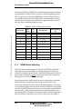
Table 1-1 High True / Low True Signal Conventions
Signal/Symbol
Logic State
Signal State
Voltage
PIN1
True
Asserted
VCC3
PIN1
False
Deasserted
Ground2
PIN1
True
Asserted
Ground2
PIN1
False
Deasserted
VCC3
Note:
Note:
PIN is a generic term for any pin on the device.
Ground is an acceptable low voltage level. See the appropriate data sheet for the range of
acceptable low voltage levels (typically a TTL logic low).
VCC is an acceptable high voltage level. See the appropriate data sheet for the range of
acceptable high voltage levels (typically a TTL logic high).
Note:
1.2
DSP56009 FEATURES
The DSP56009 consists of the DSP56000 core, program and data memory, and
peripherals useful for embedded control applications. The following paragraphs
provide a list of DSP56009 features and a brief description of its core and peripheral
components.
• General Features
1-6
–
Harvard architecture, with four 24-bit internal data buses and three 16-bit
internal address buses, permitting simultaneous accesses to program
memory and two data memories
–
Software-programmable, Phase Lock Loop (PLL) frequency synthesizer for
the core clock with a wide range of frequency multiplications (1 to 4096)
and power-saving clock divider (2i, where i = 0 to 15) for reduced clock
noise
–
On-Chip Emulation (OnCE) port for unobtrusive, comprehensive,
processor speed-independent hardware/software debugging
–
Stop and Wait low-power standby modes
–
Efficient, object code compatible, 24-bit 56000-family DSP engine
DSP56009 User’s Manual
For More Information On This Product,
Go to: www.freescale.com
MOTOROLA
Freescale Semiconductor, Inc.
Overview
Freescale Semiconductor, Inc...
DSP56009 Features
–
Up to 40.5 Million Instructions Per Second (MIPS)—24.69 ns instruction
cycle at 81 MHz
–
Up to 324 Million Operations Per Second (MOPS) at 81 MHz
–
On-chip peripheral registers memory-mapped in data memory space
–
Three external interrupt request pins
–
Data Arithmetic Logic Unit (ALU), Program Control (PC), and Address
Generation Unit (AGU) all integral to the core processor
–
Bootstrap loading from SHI or EMI (in absolute SRAM mode)
–
Completely pin-compatible with DSP56004 and DSP56007 for easy
upgrades
–
Fully static, HCMOS design for operating frequencies from 81 MHz down
to DC
–
80-pin plastic Quad Flat Pack surface-mount package; 14 × 14 × 2.45 mm;
0.65 mm lead pitch
–
Highly parallel instruction set with unique DSP addressing modes
–
Two 56-bit accumulators, including extension byte
–
Parallel 24 × 24-bit multiply-accumulate in 1 instruction cycle (2 clock
cycles)
–
Double precision 48 × 48-bit multiply with 96-bit result in 6 instruction
cycles
–
56-bit addition/subtraction in 1 instruction cycle
–
Fractional and integer arithmetic with support for multiprecision
arithmetic
–
Hardware support for block-floating point Fast Fourier Transforms (FFTs)
–
Zero-overhead fast interrupts (2 instruction cycles)
–
Nested hardware DO loops
• Memory Modules:
–
On-chip 4352 × 24-bit Y data RAM and 1792 × 24-bit Y data ROM
–
On-chip 4608 × 24-bit X data RAM and 3072 × 24-bit X data ROM
–
On-chip 10240 × 24-bit Program ROM
–
On-chip 512 × 24-bit Program RAM and 64 × 24-bit bootstrap ROM
MOTOROLA
DSP56009 User’s Manual
For More Information On This Product,
Go to: www.freescale.com
1-7
Freescale Semiconductor, Inc.
Overview
DSP56009 Architectural Overview
–
Up to 2304 × 24-Bit from X and Y data RAM can be switched to Program
RAM for a total of 2816 × 24-bit Program RAM
• Peripheral modules:
–
External Memory Interface (EMI), implemented as a peripheral,
supporting:
• Direct connection of page-mode DRAMs: 64 K × 4 bits, 64 K × 8 bits, 256
K × 4 bits, 256 K × 8 bits, 1 M × 4 bits, 1 M × 8 bits, 4 M × 4 bits, and 4 M
× 8 bits
Freescale Semiconductor, Inc...
• SRAMs (one to four): 256 K × 8 bits
• Bootstrap from EPROM
• Data bus may be 4 or 8 bits wide
• Data words may be 8, 12, 16, 20, or 24 bits wide
1.3
–
Serial Host Interface (SHI): SPI and I2C protocols, single master capability,
10-word receive FIFO register, support for 8-, 16-, and 24-bit words
–
Serial Audio Interface (SAI) includes two receivers and three transmitters,
master or slave capability, and implementation of Philips, Sony, and
Matsushita audio protocols; two complete sets of SAI interrupt vectors
–
Four independent, programmable GPIO lines
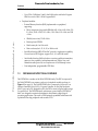
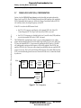
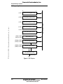
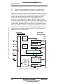
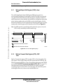
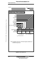
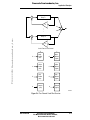
DSP56009 ARCHITECTURAL OVERVIEW
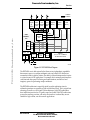
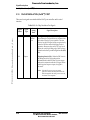
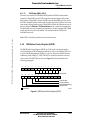
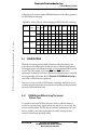
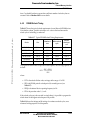
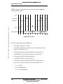
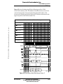
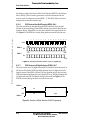
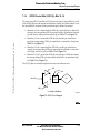
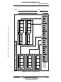
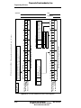
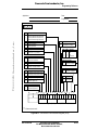
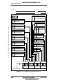
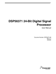
The DSP56009 is a member of the 24-bit DSP56000 family. The DSP is composed of
the 24-bit DSP56000 core, memory, and a set of peripheral modules as shown in
Figure 1-1 on page 1-9. The 24-bit DSP56000 core is composed of a Data ALU, an
Address Generation Unit (AGU), a Program Controller, an On-Chip Emulation
(OnCE) port, and a PLL designed to allow the DSP to run at full speed while using a
low-speed clock. The DSP56000-family architecture, upon which the DSP56009 is
built, was designed to maximize throughput in data-intensive digital signal
processing applications. The result is a dual-natured, expandable architecture with
sophisticated on-chip peripherals and versatile GPIO.
1-8
DSP56009 User’s Manual
For More Information On This Product,
Go to: www.freescale.com
MOTOROLA
Freescale Semiconductor, Inc.
Overview
DSP56009 Architectural Overview
4
General
Purpose
I/O
Freescale Semiconductor, Inc...
(GPIO)
Serial
Audio
Interface
(SAI)
Serial
Host
Interface
(SHI)
16-Bit Bus
24-Bit Bus
29
External
Memory
Interface
(EMI)
Program
Memory
X Data
Memory
Y Data
Memory
PAB
XAB
YAB
Address
Generation
Unit
24-Bit
DSP56000
Core
GDB
Internal
Data
Bus
Switch
PDB
XDB
YDB
OnCETM Port
Program
Decode
Controller
Interrupt
Control
Clock
PLL
Gen.
3
5
9
Program Control Unit
4
Program
Address
Generator
Data ALU
24 × 24 + 56 → 56-Bit MAC
Two 56-Bit Accumulators
4
IRQA, IRQB
NMI, RESET
AA0248k
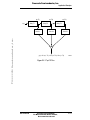
Figure 1-1 DSP56009 Block Diagram
The DSP56000 core is dual-natured in that there are two independent, expandable
data memory spaces, two address arithmetic units, and a Data ALU that has two
accumulators and two shifter/limiters. The duality of the architecture makes it easier
to write software for DSP applications. For example, data is naturally partitioned into
coefficient and data spaces for filtering and transformations, and into real and
imaginary spaces for performing complex arithmetic.
The DSP56000 architecture is especially suited for audio applications since its
arithmetic operations are executed on 24-bit or 48-bit data words. This is a significant
advantage for audio over 16-bit and 32-bit architectures: 16-bit DSP architectures
have insufficient precision for CD-quality sound, and while 32-bit DSP architectures
possess the necessary precision, with extra silicon and cost overhead they are not
suitable for high-volume, cost-driven audio applications.
MOTOROLA
DSP56009 User’s Manual
For More Information On This Product,
Go to: www.freescale.com
1-9
Freescale Semiconductor, Inc.
Overview
DSP56009 Architectural Overview
1.3.1
Memory and Peripheral Modules
Freescale Semiconductor, Inc...
The following memory and peripheral modules are included on the DSP56009:
• External Memory Interface (EMI)—The EMI provides simple connection to
external DRAM and/or SRAM and/or EPROM memories. This memory
interface is designed to provide a simple and inexpensive connection to large
DRAM memories (up to two 4 M × 4 bits) for audio delay lines. The port is
configurable as either 4 or 8 bits wide, providing a convenient interface to
standard DRAM, EPROM, and SRAM parts. Data word packing/unpacking is
automatic to simplify and accelerate converting between memory word size
and data word size. Absolute addressing can be used for random memory
access, program bootstrap, overlays, and to access external peripherals.
Relative addressing, assisted by base-offset registers, can easily be used to set
up delay lines.
• Serial Host Interface (SHI)—The SHI provides a fast, yet simple serial
interface to connect the DSP56009 to a host processor or to another serial
peripheral device. Two serial protocols are available: the Motorola Serial
Peripheral Interface (SPI) bus and the Philips Inter Integrated-circuit Control
(I2C) bus. The SHI will operate with 8-, 16-, and 24-bit words and the receiver
has an optimal 10-word FIFO register to reduce the receive interrupt rate.
• Serial Audio Interface (SAI)—The SAI provides a synchronous serial
interface that allows the DSP56009 to communicate using a wide range of
standard serial data formats used by audio manufacturers at bit rates up to
one-third the DSP core clock rate (e.g., 27 MHz for a 81 MHz clock). There are
three synchronized data transmission lines and two synchronized data
reception lines, all of which are double-buffered.
• General Purpose Input/Output (GPIO)—The GPIO has four dedicated
signals that can be independently programmed to be inputs, standard TTL
outputs, open collector outputs, or disconnected.
1.3.2
DSP Core Processor
The 24-bit DSP56000 core is composed of a Data ALU, an AGU, a Program Controller
(PC), and the buses that connect them together. The OnCE port and a PLL are
integral parts of this processor. Figure 1-1 on page 1-9 illustrates the DSP block
diagram, showing the components of the core processor, as well as the peripherals
specific to the DSP56009. The following paragraphs present a brief overview of the
DSP56000 core processor. For more thorough detail, refer to the DSP56000 Family
Manual.
1-10
DSP56009 User’s Manual
For More Information On This Product,
Go to: www.freescale.com
MOTOROLA
Freescale Semiconductor, Inc.
Overview
Freescale Semiconductor, Inc...
DSP56009 Architectural Overview
1.3.2.1
Data Arithmetic and Logic Unit (ALU)
The Data Arithmetic and Logic Unit (ALU) has been designed to be fast and provide
the capability to process signals having a wide dynamic range. Special circuitry has
been provided to facilitate the processing of data overflows and round-off errors. The
Data ALU performs all of the arithmetic and logical operations on data operands.
The Data ALU consists of four 24-bit input registers, two 48-bit accumulator
registers (also usable as four 24-bit accumulators), two 8-bit accumulator extension
registers, an accumulator shifter, two data shifter/limiters, and a parallel
single-cycle non-pipelined Multiply-Accumulator (MAC). Data ALU operations use
fractional two’s-complement arithmetic. Data ALU registers may be read or written
over the X Data Bus (XDB) and Y Data Bus (YDB) as 24- or 48-bit operands. The 24-bit
data words provide 144 dB of dynamic range. This is sufficient for most real-world
applications, including high-quality audio applications, since the majority of
Analog-to-Digital (A/D) and Digital-to-Analog (D/A) converters are 16 bits or less,
and certainly not greater than 24 bits. The 56-bit accumulation internal to the Data
ALU provides 336 dB of internal dynamic range, assuring no loss of precision due to
intermediate processing.
Two data shifter/limiters provide special post-processing on data reads (from the
ALU accumulator registers and directed to the XDB or YDB). The data shifters are
capable of shifting data one bit to the left or to the right as well as passing the data
unshifted. Each data shifter has a 24-bit output with overflow indication. The data
shifters are controlled by scaling-mode bits. These shifters permit no-overhead
dynamic scaling of fixed point data by simply programming the scaling mode bits.
This permits block floating-point algorithms to be implemented efficiently. For
example, Fast Fourier Transform (FFT) routines can use this feature to selectively
scale each butterfly pass. Saturation arithmetic is accommodated to minimize errors
due to overflow. Overflow occurs when a source operand requires more bits for
accurate representation than there are available in the destination. To minimize the
error due to overflow, “limiting” causes the maximum (or minimum, if negative)
value to be written to the destination with an error flag.
1.3.2.2
Address Generation Unit (AGU)
The Address Generation Unit (AGU) performs all address storage and effective
address calculations necessary to access data operands in memory. It implements
three types of arithmetic to update addresses—linear, modulo, and reverse carry.
This unit operates in parallel with other chip resources to minimize address
generation overhead. The AGU contains eight address registers R[7:0] (i.e., Rn), eight
offset registers N[7:0] (i.e., Nn), and eight modifier registers M[7:0] (i.e., Mn). The Rn
are 16-bit registers that may contain an address or data. Each Rn register may
provide addresses to the X memory Address Bus (XAB), Y memory Address Bus
(YAB), and the Program Address Bus (PAB). The Nn and Mn registers are 16-bit
registers that are normally used to update the Rn registers, but may be used for data.
MOTOROLA
DSP56009 User’s Manual
For More Information On This Product,
Go to: www.freescale.com
1-11
Freescale Semiconductor, Inc.
Overview
DSP56009 Architectural Overview
Freescale Semiconductor, Inc...
AGU registers may be read from or written to via the Global Data Bus as 16-bit
operands. The AGU has two modulo arithmetic units that can generate two
independent 16-bit addresses every instruction cycle for any two of the XAB, YAB, or
PAB.
1.3.2.3
Program Control Unit
The program control unit performs instruction prefetch, instruction decoding,
hardware DO loop control, and exception processing. It contains six directly
addressable registers—the Program Counter (PC), Loop Address (LA), Loop Counter
(LC), Status Register (SR), Operating Mode Register (OMR), and Stack Pointer (SP).
The program control unit also contains a 15 level by 32-bit system stack memory. The
16-bit PC can address 65,536 (64 K) locations in program memory space.
1.3.2.4
Data Buses
Data movement on the chip occurs over four bidirectional 24-bit buses—the X Data
Bus (XDB), the Y Data Bus (YDB), the Program Data Bus (PDB), and the Global Data
Bus (GDB). Certain instructions concatenate XDB and YDB to form a 48-bit data bus.
Data transfers between the Data ALU and the two data memories, X and Y, occur
over the XDB and YDB, respectively. These transfers can occur simultaneously on the
DSP, maximizing data throughput. All other data transfers, such as I/O transfers to
internal peripherals, occur over the GDB. Instruction word pre-fetches take place
over the PDB in parallel with data transfers. Transfers between buses are
accomplished through the internal bus switch.
1.3.2.5
Address Buses
Addresses are specified for internal X data memory and Y data memory using two
unidirectional 16-bit buses—the X Address Bus (XAB) and the Y Address Bus (YAB).
program memory addresses are specified using the 16-bit Program Address Bus
(PAB).
1.3.2.6
Phase Lock Loop (PLL)
The Phase Lock Loop (PLL) reduces the need for multiple oscillators in a system
design, thus reducing the overall system cost. An additional benefit of the PLL is that
it permits the use of a low-frequency external clock with no sacrifice of processing
speed. The PLL converts the low-frequency external clock to the high speed internal
clock needed to run the DSP at maximum speed. This diminishes the electromagnetic
interference generated by high frequency clocking. The PLL performs frequency
multiplication to allow the processor to use almost any available external system
clock for full-speed operation. It also improves the synchronous timing of the
processor’s external memory port, significantly reducing the timing skew between
EXTAL and the internal chip phases when the Multiplication Factor (MF) ≤ 4. The
PLL is unique in that it provides a low power divider on its output, which can reduce
or restore the chip operating frequency without losing the PLL lock.
1-12
DSP56009 User’s Manual
For More Information On This Product,
Go to: www.freescale.com
MOTOROLA
Freescale Semiconductor, Inc.
Overview
DSP56009 Architectural Overview
1.3.2.7
On-Chip Emulation (OnCE) Port
The On-Chip Emulation (OnCE) port provides a sophisticated debugging tool that
allows simple, inexpensive, and speed-independent access to the processor’s internal
registers and peripherals. The OnCE port tells the application programmer the exact
status of most of the on-chip registers, memory locations, and buses, as well as
storing the addresses of the last five instructions that were executed.
Freescale Semiconductor, Inc...
1.3.3
Memories
The three independent memory spaces of the DSP56009—X data, Y data, and
program—and their configurations are discussed briefly here. See Section 3,
Memory, Operating Modes, and Interrupts for more detail.
1.3.3.1
Program Memory
The on-chip program memory is 24-bits wide. Addresses are received from the
Program Control Logic (usually the Program Counter) over the Program Address
Bus (PAB). Program memory may be written using MOVEM instructions. The
interrupt vectors are located in the bottom 128 locations of program memory.
Table 1-2 lists the interrupt vector addresses and indicates the Interrupt Priority
Level (IPL) of each interrupt source.
Program RAM has many advantages. It provides a means to develop code efficiently.
Programs can be changed dynamically, allowing efficient overlaying of DSP software
algorithms. In this way the on-chip Program RAM operates as a fixed cache, thereby
minimizing accesses to slower external memory.
The Bootstrap mode, described in Appendix A, provides a convenient, low-cost
method to load the DSP56009 Program RAM from a single, inexpensive EPROM
connected to the EMI, or through the SHI, using either SPI or I2C formats, after a
power-on reset.
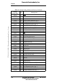
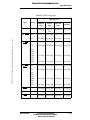
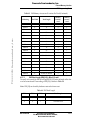
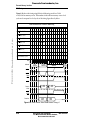
Table 1-2 Interrupt Starting Addresses and Sources
Interrupt
Starting Address
IPL
P:$0000
3
Hardware RESET
P:$0002
3
Stack Error
P:$0004
3
Trace
P:$0006
3
SWI
P:$0008
0–2
MOTOROLA
Interrupt Source
IRQA
DSP56009 User’s Manual
For More Information On This Product,
Go to: www.freescale.com
1-13
Freescale Semiconductor, Inc.
Overview
DSP56009 Architectural Overview
Table 1-2 Interrupt Starting Addresses and Sources (Continued)
IPL
P:$000A
0–2
Freescale Semiconductor, Inc...
Interrupt
Starting Address
IRQB
P:$000C
Reserved
P:$000E
Reserved
P:$0010
0–2
SAI Left Channel Transmitter if TXIL = 0
P:$0012
0–2
SAI Right Channel Transmitter if TXIL = 0
P:$0014
0–2
SAI Transmitter Exception if TXIL = 0
P:$0016
0–2
SAI Left Channel Receiver if RXIL = 0
P:$0018
0–2
SAI Right Channel Receiver if RXIL = 0
P:$001A
0–2
SAI Receiver Exception if RXIL = 0
P:$001C
Reserved
P:$001E
3
P:$0020
0–2
SHI Transmit Data
P:$0022
0–2
SHI Transmit Underrun Error
P:$0024
0–2
SHI Receive FIFO Not Empty
P:$0026
NMI
Reserved
P:$0028
0–2
SHI Receive FIFO Full
P:$002A
0–2
SHI Receive Overrun Error
P:$002C
0–2
SHI Bus Error
P:$002E
1-14
Interrupt Source
Reserved
P:$0030
0–2
EMI Write Data
P:$0032
0–2
EMI Read Data
P:$0034
0–2
EMI EBAR0 Memory Wrap
P:$0036
0–2
EMI EBAR1 Memory Wrap
P:$0038
Reserved
P:$003A
Reserved
P:$003C
Reserved
P:$003E
3
Illegal Instruction
P: $0040
0–2
SAI Left Channel Transmitter if TXIL = 1
P: $0042
0–2
SAI Right Channel Transmitter if TXIL = 1
P: $0044
0–2
SAI Transmitter Exception if TXIL = 1
P: $0046
0–2
SAI Left Channel Receiver if RXIL = 1
P: $0048
0–2
SAI Right Channel Receiver if RXIL = 1
DSP56009 User’s Manual
For More Information On This Product,
Go to: www.freescale.com
MOTOROLA
Freescale Semiconductor, Inc.
Overview
DSP56009 Architectural Overview
Table 1-2 Interrupt Starting Addresses and Sources (Continued)
Interrupt
Starting Address
IPL
P: $004A
0–2
Interrupt Source
SAI Receiver Exception if RXIL = 1
P: $004C
Reserved
:
:
Freescale Semiconductor, Inc...
P: $007E
Reserved
1.3.3.2
X Data Memory
The on-chip X data memory is 24 bits wide. Addresses are received from the XAB,
and data transfers to the Data ALU occur on the XDB.
1.3.3.3
Y Data Memory
The on-chip Y data memory is 24 bits wide. Addresses are received from the YAB,
and data transfers to the Data ALU occur on the YDB.
1.3.3.4
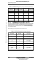
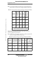
On-Chip Memory Configuration Bits
Through the use of bits PEA and PEB in the OMR, four different memory
configurations are possible. These configurations provide appropriate memory sizes
for a variety of applications (see Table 1-3). Section 3 provides detailed information
about memory configuration.
Table 1-3 Internal Memory Configurations
No Switch
(PEA = 0,
PEB = 0)
Switch A
(PEA = 1,
PEB = 0)
Switch B
(PEA = 0,
PEB = 1)
Switch A + B
(PEA = 1,
PEB = 1)
Program RAM
0.5 K
1.25 K
2.0 K
2.75 K
X data RAM
4.5 K
3.75 K
3.75 K
3.0 K
Y data RAM
4.25 K
4.25 K
3.5 K
3.5 K
Program ROM
10.0 K
10.0 K
10.0 K
10.0 K
X data ROM
3.0 K
3.0 K
3.0 K
3.0 K
Y data ROM
1.75 K
1.75 K
1.75 K
1.75 K
1.3.3.5
Bootstrap ROM
The bootstrap ROM occupies locations 0–31 ($0–$1F) and 256–287 ($100–$11F) in two
areas in the memory map on the DSP56009. The bootstrap ROM is
factory-programmed to perform the bootstrap operation following hardware reset; it
either jumps to the user’s ROM starting address (P:$2000) or downloads up to 512
words of user program from either the EMI port or the SHI port (in SPI or I2C
format). The bootstrap ROM activity is controlled by the bits MA, MB, and MC,
MOTOROLA
DSP56009 User’s Manual
For More Information On This Product,
Go to: www.freescale.com
1-15
Freescale Semiconductor, Inc.
Overview
DSP56009 Architectural Overview
which are located in the OMR. When in the Bootstrap mode, the first 512 words of
Program RAM are read-disabled but write-accessible. The contents of the bootstrap
ROM are listed in Appendix A.
Freescale Semiconductor, Inc...
1.3.3.6
External Memory
The DSP56009 does not extend internal memory off chip. However, external memory
can be added using the EMI. See Section 4, External Memory Interface for a detailed
description of the EMI.
1.3.3.7
Reserved Memory Spaces
The memory spaces marked as reserved should not be accessed by the user. They are
reserved for the expansion of future versions or variants of this DSP. Write
operations to the reserved range are ignored. Read operations from addresses in the
reserved range (with values greater than or equal to $2C00 in X memory space and
$2700 in Y memory space, and values from the reserved area of program memory
space), return the value $000005, which is the opcode for the ILLEGAL instruction. If
a read access is performed from the reserved area below address $2000 in X or Y data
memory, the resulting data will be undetermined. If an instruction fetch is attempted
from addresses in the reserved area, the value returned is $000005, which is the
opcode for the ILLEGAL instruction, causing an illegal instruction interrupt service.
1.3.4
Input/Output
A variety of system configurations are facilitated by the DSP56009 Input/Output
(I/O) structure. Each I/O interface has its own control, status, and double-buffered
data registers that are memory-mapped in the X data memory space (see Table 1-4).
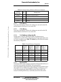
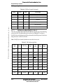
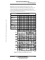
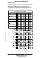
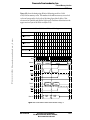
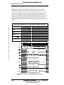
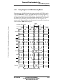
Table 1-4 On-chip Peripheral Memory Map
Address
Register
X:$FFFF
Interrupt Priority Register (IPR)
X:$FFFE
Reserved
X:$FFFD
PLL Control Register (PCTL)
X:$FFFC
Reserved
X:$FFFB
Reserved
X:$FFFA
Reserved
X:$FFF9
Reserved
X:$FFF8
Reserved
X:$FFF7
GPIO Control/Data Register (GPIOR)
1-16
DSP56009 User’s Manual
For More Information On This Product,
Go to: www.freescale.com
MOTOROLA
Freescale Semiconductor, Inc.
Overview
DSP56009 Architectural Overview
Table 1-4 On-chip Peripheral Memory Map (Continued)
Freescale Semiconductor, Inc...
Address
Register
X:$FFF6
EMI Write Offset Register (EWOR)
X:$FFF5
Reserved
X:$FFF4
Reserved
X:$FFF3
SHI Receive FIFO/Transmit Register (HRX/HTX)
X:$FFF2
SHI I2C Slave Address Register (HSAR)
X:$FFF1
SHI Host Control/Status Register (HCSR)
X:$FFF0
SHI Host Clock Control Register (HCKR)
X:$FFEF
EMI Refresh Control Register (ERCR)
X:$FFEE
EMI Data Register 1 (EDRR1/EDWR1)
X:$FFED
EMI Offset Register 1 (EOR1)
X:$FFEC
EMI Base Address Register 1 (EBAR1)
X:$FFEB
EMI Control/Status Register (ECSR)
X:$FFEA
EMI Data Register 0 (EDRR0/EDWR0)
X:$FFE9
EMI Offset Register 0 (EOR0)
X:$FFE8
EMI Base Address Register 0 (EBAR0)
X:$FFE7
SAI TX2 Data Register (TX2)
X:$FFE6
SAI TX1 Data Register (TX1)
X:$FFE5
SAI TX0 Data Register (TX0)
X:$FFE4
SAI TX Control/status Register (TCS)
X:$FFE3
SAI RX1 Data Register (RX1)
X:$FFE2
SAI RX0 Data Register (RX0)
X:$FFE1
SAI RX Control/Status Register (RCS)
X:$FFE0
SAI Baud Rate Control Register (BRC)
X:$FFDF
Reserved
:
:
X:$FFC0
Reserved
The EMI, SHI, and SAI also have several dedicated interrupt vector addresses and
control bits to enable and disable interrupts (see Table 1-2 on page 1-13). These
interrupt vectors minimize the overhead associated with servicing an interrupt by
immediately executing the appropriate service routine. Each interrupt can be
programmed to one of three maskable priority levels.
MOTOROLA
DSP56009 User’s Manual
For More Information On This Product,
Go to: www.freescale.com
1-17
Freescale Semiconductor, Inc.
Overview
DSP56009 Architectural Overview
1.3.4.1
External Memory Interface
The External Memory Interface (EMI) is an I/O interface that enables the DSP to
access external dynamic and/or static memory with little or no additional logic. The
EMI is implemented as a buffered peripheral rather than a transparent extension to
internal memory. This interface facilitates the storage of audio samples for digital
reverberation algorithms and permits simple implementation of large data delay
buffers in external memory. The EMI on the DSP56009 is designed to connect directly
to Dynamic RAM (DRAM) of the following sizes:
Freescale Semiconductor, Inc...
• One or two 256 K × 4 bit chips
• One or two 1 M × 4 bit chips
• One or two 4 M × 4 bits chips
When using Static RAM (SRAM), the EMI may directly access up to 256 K × 8 bits.
The external data bus width may be 4 or 8 bits. Data words of 8, 12, 16, 20 or 24 bits
may be stored and retrieved via the EMI with automatic packing and unpacking. In
addition, the EMI may be selected to operate in the SRAM/EPROM absolute
addressing mode. This allows connection to external memory devices for program
bootstrap and data storage, as well as general parallel access to peripheral devices.
1.3.4.2
Serial Host Interface (SHI)
The Serial Host Interface (SHI) provides a serial path for communication and
program/coefficient data transfers between the DSP and an external host processor
or other serial peripheral devices. This interface can connect directly to one of two
well-known and widely-used synchronous serial buses: the Serial Peripheral
Interface (SPI) bus defined by Motorola and the Inter Integrated-circuit Control (I2C)
bus defined by Philips. The SHI handles both SPI and I2C bus protocols as required
from a slave or a single-master device. In order to minimize DSP overhead, the SHI
supports single-, double-, and triple-byte data transfers. An optimal ten-word receive
FIFO register reduces the DSP overhead for data reception.
1-18
DSP56009 User’s Manual
For More Information On This Product,
Go to: www.freescale.com
MOTOROLA
Freescale Semiconductor, Inc.
Overview
DSP56009 Architectural Overview
1.3.4.3
Serial Audio Interface (SAI)
The DSP can communicate with other devices through the SAI. The SAI provides a
synchronous full-duplex serial port for serial connection with a variety of audio
devices such as Analog-to-Digital (A/D) converters, Digital-to-Analog (D/A)
converters, Compact Disk (CD) devices, etc. The SAI implements a wide range of
serial data formats in use by audio manufacturers. Examples are:
• I2S format (Philips)
• CDP format (Sony)
Freescale Semiconductor, Inc...
• MEC format (Matsushita)
• Most industry-standard serial A/D and D/A formats
The SAI consists of independent transmit and receive sections and a common baud
rate generator. The transmitter consists of three transmitters controlled by one
transmitter controller. This enables simultaneous data transmission to as many as
three stereo audio devices, or transmission of three separate stereo pairs of audio
channels. The receiver consists of two receivers and a single receive controller. This
enables simultaneous data reception from up to two stereo audio devices. The
transmit and receive sections are fully asynchronous and may transmit and receive at
different rates.
1.3.4.4
General Purpose Input/Output
The General Purpose Input/Output (GPIO) signals are used for control and
handshake functions between the DSP and external circuitry. The GPIO port has four
dedicated signals (GPIO0–GPIO3) that are controlled through a memory-mapped
register. Associated with each GPIO signal is a data bit, a control bit, and a data
direction bit that configures the pin as an input or an output, open-collector or
normal. See Section 7 for detailed information about GPIO operation.
MOTOROLA
DSP56009 User’s Manual
For More Information On This Product,
Go to: www.freescale.com
1-19
Freescale Semiconductor, Inc.
Overview
Freescale Semiconductor, Inc...
DSP56009 Architectural Overview
1-20
DSP56009 User’s Manual
For More Information On This Product,
Go to: www.freescale.com
MOTOROLA
Freescale Semiconductor, Inc.
SECTION 2
Freescale Semiconductor, Inc...
SIGNAL DESCRIPTIONS
MOTOROLA
DSP56009 User’s Manual
For More Information On This Product,
Go to: www.freescale.com
2-1
Freescale Semiconductor, Inc.
Freescale Semiconductor, Inc...
Signal Descriptions
2.1
2.2
2.3
2.4
2.5
2.6
2.7
2.8
2.9
2.10
2-2
SIGNAL GROUPINGS . . . . . . . . . . . . . . . . . . . . . . . . . . . . . . . . 2-3
POWER . . . . . . . . . . . . . . . . . . . . . . . . . . . . . . . . . . . . . . . . . . . . . 2-5
GROUND. . . . . . . . . . . . . . . . . . . . . . . . . . . . . . . . . . . . . . . . . . . . 2-5
CLOCK AND PLL SIGNALS . . . . . . . . . . . . . . . . . . . . . . . . . . . 2-6
EXTERNAL MEMORY INTERFACE (EMI) . . . . . . . . . . . . . . . 2-7
INTERRUPT AND MODE CONTROL . . . . . . . . . . . . . . . . . . . 2-10
SERIAL HOST INTERFACE (SHI). . . . . . . . . . . . . . . . . . . . . 2-14
SERIAL AUDIO INTERFACE (SAI) . . . . . . . . . . . . . . . . . . . 2-18
GENERAL PURPOSE I/O . . . . . . . . . . . . . . . . . . . . . . . . . . . . 2-21
ON-CHIP EMULATION (OnCE TM) PORT. . . . . . . . . . . . . . . 2-22
DSP56009 User’s Manual
For More Information On This Product,
Go to: www.freescale.com
MOTOROLA
Freescale Semiconductor, Inc.
Signal Descriptions
Signal Groupings
2.1
SIGNAL GROUPINGS
The DSP56009 input and output signals are organized into the nine functional
groups, as shown in Table 2-1. The individual signals are illustrated in Figure 2-1.
Table 2-1 DSP56009 Functional Group Signal Allocations
Number of Signals
Detailed
Description
Power (VCC)
9
Table 2-2
Ground (GND)
13
Table 2-3
Phase Lock Loop (PLL)
3
Table 2-4
External Memory Interface (EMI)
29
Table 2-5 and
Table 2-6
Interrupt and Mode Control
4
Table 2-7
Serial Host Interface (SHI)
5
Table 2-8
Serial Audio Interface (SAI)
9
Table 2-9 and
Table 2-10
General Purpose Input/Output (GPIO)
4
Table 2-11
On-Chip Emulation (OnCE) port
4
Table 2-12
Freescale Semiconductor, Inc...
Functional Group
Total
MOTOROLA
80
DSP56009 User’s Manual
For More Information On This Product,
Go to: www.freescale.com
2-3
Freescale Semiconductor, Inc.
Signal Descriptions
Signal Groupings
Power Inputs
VCCP
3
VCCQ
2
VCCA
VCCD
2
VCCS
Ground
GNDP
Freescale Semiconductor, Inc...
GNDQ
GNDA
GNDD
GNDS
DSP56009
MOSI/HA0
SS/HA2
Port B
Serial Host
Interface
MISO/SDA
SCK/SCL
HREQ
3
4
2
3
Port C
Serial Audio
Interface
WSR
PCAP
SCKR
PINIT
PLL
Rec0
Rec1
EXTAL
SDI0
SDI1
WST
MA0–MA14
MD0–MD7
SCKT
15
8
MA15/MCS3
MA16/MCS2/MCAS
MA17/MCS1/MRAS
MCS0
Tran0
SDO0
Tran1
SDO1
Tran2
SDO2
Port A
External Memory
Interface
GPIO
MWR
4
GPIO0–GPIO3
MRD
DSCK/OS1
MODC/NMI
MODB/IRQB
MODA/IRQA
RESET
Mode/Interrupt
Control
OnCE™
Port
Reset
DSI/OS0
DSO
DR
80 signals
AA0249G
Figure 2-1 DSP56009 SIgnals
2-4
DSP56009 User’s Manual
For More Information On This Product,
Go to: www.freescale.com
MOTOROLA
Freescale Semiconductor, Inc.
Signal Descriptions
Power
2.2
POWER
Table 2-2 Power Inputs
Freescale Semiconductor, Inc...
Power Name
Description
VCCP
PLL Power —VCCP provides isolated power for the Phase Lock Loop
(PLL). The voltage should be well-regulated and the input should be
provided with an extremely low impedance path to the VCC power rail.
VCCQ
Quiet Power—VCCQ provides isolated power for the internal processing
logic. This input must be tied externally to all other chip power inputs.
The user must provide adequate external decoupling capacitors.
VCCA
Address Bus Power —VCCA provides isolated power for sections of the
address bus I/O drivers. This input must be tied externally to all other
chip power inputs. The user must provide adequate external decoupling
capacitors.
VCCD
Data Bus Power —VCCD provides isolated power for sections of the data
bus I/O drivers. This input must be tied externally to all other chip
power inputs. The user must provide adequate external decoupling
capacitors.
VCCS
Serial Interface Power —VCCS provides isolated power for the SHI and
SAI. This input must be tied externally to all other chip power inputs. The
user must provide adequate external decoupling capacitors.
2.3
GROUND
Table 2-3 Grounds
Ground Name
Description
GNDP
PLL Ground —GNDP is ground dedicated for PLL use. The connection
should be provided with an extremely low-impedance path to ground.
VCCP should be bypassed to GNDP by a 0.47 µF capacitor located as close
as possible to the chip package.
GNDQ
Quiet Ground —GNDQ provides isolated ground for the internal
processing logic. This connection must be tied externally to all other chip
ground connections. The user must provide adequate external
decoupling capacitors.
GNDA
Address Bus Ground —GNDA provides isolated ground for sections of
the address bus I/O drivers. This connection must be tied externally to all
other chip ground connections. The user must provide adequate external
decoupling capacitors.
MOTOROLA
DSP56009 User’s Manual
For More Information On This Product,
Go to: www.freescale.com
2-5
Freescale Semiconductor, Inc.
Signal Descriptions
Clock and PLL signals
Table 2-3 Grounds (Continued)
Freescale Semiconductor, Inc...
Ground Name
Description
GNDD
Data Bus Ground —GNDD provides isolated ground for sections of the
data bus
I/O drivers. This connection must be tied externally to all other chip
ground connections. The user must provide adequate external
decoupling capacitors.
GNDS
Serial Interface Ground —GNDS provides isolated ground for the SHI and SAI.
This connection must be tied externally to all other chip ground connections. The
user must provide adequate external decoupling capacitors.
2.4
CLOCK AND PLL SIGNALS
Note: While the PLL on this DSP is identical to the PLL described in the DSP56000
Family Manual, two of the signals have not been implemented externally.
Specifically, there is no PLOCK signal or CKOUT signal available. Therefore,
the internal clock is not directly accessible and there is no external indication
that the PLL is locked. These signals were omitted to reduce the number of
pins and allow this DSP to be put in a smaller, less expensive package.
Table 2-4 Clock and PLL Signals
Signal
Name
EXTAL
2-6
Signal
Type
Input
State
during
Reset
Input
Signal Description
External Clock/Crystal —This input should be connected
to an external clock source. If the PLL is enabled, this
signal is internally connected to the on-chip PLL. The PLL
can multiply the frequency on the EXTAL pin to generate
the internal DSP clock. The PLL output is divided by two
to produce a four-phase instruction cycle clock, with the
minimum instruction time being two PLL output clock
periods. If the PLL is disabled, EXTAL is divided by two
to produce the four-phase instruction cycle clock.
DSP56009 User’s Manual
For More Information On This Product,
Go to: www.freescale.com
MOTOROLA
Freescale Semiconductor, Inc.
Signal Descriptions
External Memory Interface (EMI)
Table 2-4 Clock and PLL Signals (Continued)
Signal
Name
Freescale Semiconductor, Inc...
PCAP
Signal
Type
Input
State
during
Reset
Input
Signal Description
PLL Filter Capacitor—This input is used to connect a
high-quality (high “Q” factor) external capacitor needed
for the PLL filter. The capacitor should be as close as
possible to the DSP with heavy, short traces connecting
one terminal of the capacitor to PCAP and the other
terminal to VCCP. The required capacitor value is
specified in the DSP56009 Technical Data sheets.
When short lock time is critical, low dielectric absorption
capacitors such as polystyrene, polypropylene, or teflon
are recommended.
If the PLL is not used (i.e., it remains disabled at all
times), there is no need to connect a capacitor to the
PCAP pin. It may remain unconnected, or be tied to
either Vcc or GND.
PINIT
2.5
Input
Input
PLL Initialization (PINIT)—During the assertion of
hardware reset, the value on the PINIT line is written into
the PEN bit of the PCTL register. When set, the PEN bit
enables the PLL by causing it to derive the internal clocks
from the PLL voltage controlled oscillator output. When
the bit is cleared, the PLL is disabled and the DSP’s
internal clocks are derived from the clock connected to
the EXTAL signal. After hardware RESET is deasserted,
the PINIT signal is ignored.
EXTERNAL MEMORY INTERFACE (EMI)
Table 2-5 External Memory Interface (EMI) Signals
Signal Name
MA0–MA14
MOTOROLA
Signal
Type
State
during
Reset
Output
Table 2-6
Signal Description
Memory Address Lines 0–14—MA0–MA10
provide the multiplexed row/column
addresses for DRAM accesses and MA0–MA14
provide the non-multiplexed address lines 0–14
for SRAM accesses.
DSP56009 User’s Manual
For More Information On This Product,
Go to: www.freescale.com
2-7
Freescale Semiconductor, Inc.
Signal Descriptions
External Memory Interface (EMI)
Table 2-5 External Memory Interface (EMI) Signals (Continued)
Signal
Type
State
during
Reset
MA15/MCS3
Output
Table 2-6
Memory Address Line 15 (MA15)/Memory
Chip Select 3 (MCS3)—This line functions as
the non-multiplexed address line 15 or as
memory chip select 3 for SRAM accesses.
MA16/MCS2/
MCAS
Output
Table 2-6
Memory Address Line 16 (MA16)/Memory
Chip Select 2 (MCS2)/Memory Column
Address Strobe (MCAS)— This line functions
as the non-multiplexed address line 16 or as
memory chip select 2 for SRAM accesses. This
line also functions as the Memory Column
Address Strobe (MCAS) during DRAM
accesses.
MA17/MCS1/
MRAS
Output
Table 2-6
Memory Address Line 17 (MA17)/Memory
Chip Select 1 (MCS1)/Memory Row Address
Strobe (MRAS)—This line functions as the
non-multiplexed address line 17 or as chip
select 1 for SRAM accesses. This line also
functions as the Memory Row Address Strobe
during DRAM accesses.
MCS0
Output
Table 2-6
Memory Chip Select 0—This line functions as
memory chip select 0 for SRAM accesses.
MWR
Output
Table 2-6
Memory Write Strobe—This line is asserted
when writing to external memory.
MRD
Output
Table 2-6
Memory Read Strobe—This line is asserted
when reading external memory.
Freescale Semiconductor, Inc...
Signal Name
MD0–MD7
2-8
BiTri-stated
directional
Signal Description
Data Bus—These signals provide the
bidirectional data bus for EMI accesses. They
are inputs during reads from external memory,
outputs during writes to external memory, and
tri-stated if no external access is taking place. If
the data bus width is defined as four bits wide,
only signals MD0–MD3 are active, while signals
MD4–MD7 remain tri-stated. While tri-stated,
MD0–MD7 are disconnected from the pins and
do not require external pull-ups.
DSP56009 User’s Manual
For More Information On This Product,
Go to: www.freescale.com
MOTOROLA
Freescale Semiconductor, Inc.
Signal Descriptions
External Memory Interface (EMI)
.
Table 2-6 EMI Operating States
Operating Mode
Signal
MA0–MA14
—
Hardware
Reset
Software
Reset
Driven High
Previous
State
Individual
Reset
Stop Mode
Previous State Previous State
MA15
Driven High
Driven High Previous State Previous State
MCS3
Driven High
Driven High
MA16/MCS2/ MA16
MCAS
Driven High
Driven High Previous State Previous State
MCS2
Driven High
Driven High
Driven High
Driven High
MCAS:
DRAM
refresh
disabled
DRAM
refresh
enabled
Driven High
Driven High
Driven High
Driven High
Driven High
Driven High
Driven Low
Driven High
MA17/MCS1/ MA17
MRAS
Driven High
Driven High Previous State Previous State
MCS1
Driven High
Driven High
Driven High
Driven High
MRAS:
DRAM
refresh
disabled
DRAM
refresh
enabled
Driven High
Driven High
Driven High
Driven High
Driven High
Driven High
Driven Low
Driven High
MA15/MCS3
Freescale Semiconductor, Inc...
Function
Driven High
Driven High
MCS0
—
Driven High
Driven High
Driven High
Driven High
MWR
—
Driven High
Driven High
Driven High
Driven High
MRD
—
Driven High
Driven High
Driven High
Driven High
MOTOROLA
DSP56009 User’s Manual
For More Information On This Product,
Go to: www.freescale.com
2-9
Freescale Semiconductor, Inc.
Signal Descriptions
Interrupt and Mode Control
2.6
INTERRUPT AND MODE CONTROL
The interrupt and mode control signals select the DSP’s operating mode as it comes
out of hardware reset and receives interrupt requests from external sources after
reset.
Table 2-7 Interrupt and Mode Control Signals
Freescale Semiconductor, Inc...
Signal
Name
MODA
Signal
Type
Input
State during
Reset
Input
(MODA)
Signal Description
Mode Select A—This input signal has three
functions:
•
•
•
to work with the MODB and MODC signals
to select the DSP’s initial operating mode,
to allow an external device to request a DSP
interrupt after internal synchronization, and
to turn on the internal clock generator when
the DSP in the Stop processing state, causing
the DSP to resume processing.
MODA is read and internally latched in the DSP
when the processor exits the Reset state. The logic
state present on the MODA, MODB, and MODC pins
selects the initial DSP operating mode. Several clock
cycles after leaving the Reset state, the MODA signal
changes to the external interrupt request IRQA. The
DSP operating mode can be changed by software
after reset.
IRQA
External Interrupt Request A (IRQA)—The IRQA
input is a synchronized external interrupt request. It
may be programmed to be level-sensitive or
negative-edge-triggered. When the signal is edge
triggered, triggering occurs at a voltage level and is
not directly related to the fall time of the interrupt
signal. However, as the fall time of the interrupt
signal increases, the probability that noise on IRQA
will generate multiple interrupts also increases.
While the DSP is in the Stop mode, asserting IRQA
gates on the oscillator and, after a clock stabilization
delay, enables clocks to the processor and
peripherals. Hardware reset causes this input to
function as MODA.
2-10
DSP56009 User’s Manual
For More Information On This Product,
Go to: www.freescale.com
MOTOROLA
Freescale Semiconductor, Inc.
Signal Descriptions
Interrupt and Mode Control
Table 2-7 Interrupt and Mode Control Signals (Continued)
Signal
Name
MODB
Signal
Type
Input
State during
Reset
Input
(MODB)
Signal Description
Mode Select B— This input signal has two functions:
•
Freescale Semiconductor, Inc...
•
to work with the MODA and MODC signals
to select the DSP’s initial operating mode, and
to allow an external device to request a DSP
interrupt after internal synchronization.
MODB is read and internally latched in the DSP
when the processor exits the Reset state. The logic
state present on the MODA, MODB, and MODC pins
selects the initial DSP operating mode. Several clock
cycles after leaving the Reset state, the MODB signal
changes to the external interrupt request IRQB. The
DSP operating mode can be changed by software
after reset.
IRQB
External Interrupt Request B (IRQB)—The IRQB
input is a synchronized external interrupt request. It
may be programmed to be level-sensitive or
negative-edge-triggered. When the signal is
edge-triggered, triggering occurs at a voltage level
and is not directly related to the fall time of the
interrupt signal. However, as the fall time of the
interrupt signal increases, the probability that noise
on IRQB will generate multiple interrupts also
increases. Hardware reset causes this input to
function as MODB.
MOTOROLA
DSP56009 User’s Manual
For More Information On This Product,
Go to: www.freescale.com
2-11
Freescale Semiconductor, Inc.
Signal Descriptions
Interrupt and Mode Control
Table 2-7 Interrupt and Mode Control Signals (Continued)
Signal
Name
MODC/
NMI
Signal
Type
State during
Reset
Input,
Input
edge(MODC)
triggered
Signal Description
Mode Select C—This input signal has two functions:
•
•
to work with the MODA and MODB signals
to select the DSP’s initial operating mode, and
to allow an external device to request a DSP
interrupt after internal synchronization.
Freescale Semiconductor, Inc...
MODC is read and internally latched in the DSP
when the processor exits the Reset state. The logic
state present on the MODA, MODB, and MODC pins
selects the initial DSP operating mode. Several clock
cycles after leaving the Reset state, the MODC signal
changes to the Non-Maskable Interrupt request,
NMI. The DSP operating mode can be changed by
software after reset.
Non-Maskable Interrupt Request—The NMI input
is a negative-edge-triggered external interrupt
request. This is a level 3 interrupt that can not be
masked out. Triggering occurs at a voltage level and
is not directly related to the fall time of the interrupt
signal. However, as the fall time of the interrupt
signal increases, the probability that noise on NMI
will generate multiple interrupts also increases.
Hardware reset causes this input to function as
MODC.
2-12
DSP56009 User’s Manual
For More Information On This Product,
Go to: www.freescale.com
MOTOROLA
Freescale Semiconductor, Inc.
Signal Descriptions
Interrupt and Mode Control
Table 2-7 Interrupt and Mode Control Signals (Continued)
Signal
Name
input
Freescale Semiconductor, Inc...
RESET
Signal
Type
State during
Reset
active
Signal Description
RESET—This input causes a direct hardware reset of
the processor. When RESET is asserted, the DSP is
initialized and placed in the Reset state. A
Schmitt-trigger input is used for noise immunity. When
the reset signal is deasserted, the initial DSP operating
mode is latched from the MODA, MODB, and MODC
signals. The DSP also samples the PINIT signal and
writes its status into the PEN bit of the PLL Control
Register. When the DSP comes out of the Reset state,
deassertion occurs at a voltage level and is not
directly related to the rise time of the RESET signal.
However, the probability that noise on RESET will
generate multiple resets increases with increasing
rise time of the RESET signal.
For proper hardware reset to occur, the clock must be
active, since a number of clock ticks are required for
proper propagation of the hardware reset state.
MOTOROLA
DSP56009 User’s Manual
For More Information On This Product,
Go to: www.freescale.com
2-13
Freescale Semiconductor, Inc.
Signal Descriptions
Serial Host Interface (SHI)
2.7
SERIAL HOST INTERFACE (SHI)
The Serial Host Interface (SHI) has five I/O signals, which may be configured to
operate in either SPI or I2C mode. Table 2-8 lists the SHI signals.
Table 2-8 Serial Host Interface (SHI) signals
Freescale Semiconductor, Inc...
Signal Name
Signal
Type
SCK
Input or
Output
SCL
Input or
Output
2-14
State
during
Reset
Tri-stated
Signal Description
SPI Serial Clock (SCK)—The SCK signal is an
output when the SPI is configured as a master, and
a Schmitt-trigger input when the SPI is configured
as a slave. When the SPI is configured as a master,
the SCK signal is derived from the internal SHI
clock generator. When the SPI is configured as a
slave, the SCK signal is an input, and the clock
signal from the external master synchronizes the
data transfer. The SCK signal is ignored by the SPI
if it is defined as a slave and the Slave Select (SS)
signal is not asserted. In both the master and slave
SPI devices, data is shifted on one edge of the SCK
signal and is sampled on the opposite edge where
data is stable. Edge polarity is determined by the
SPI transfer protocol.
I2C Serial Clock (SCL)—SCL carries the clock for
bus transactions in the I2C mode. SCL is a
Schmitt-trigger input when configured as a slave,
and an open-drain output when configured as a
master. SCL should be connected to VCC through a
pull-up resistor. The maximum allowed internally
generated bit clock frequency is Fosc/4 for the SPI
mode and Fosc/6 for the I2C mode where Fosc is the
clock on EXTAL. The maximum allowed
externally generated bit clock frequency is Fosc/3
for the SPI mode and Fosc/5 for the I2C mode. This
signal is tri-stated during hardware reset, software
reset, or individual reset (no need for external
pull-up in this state).
DSP56009 User’s Manual
For More Information On This Product,
Go to: www.freescale.com
MOTOROLA
Freescale Semiconductor, Inc.
Signal Descriptions
Serial Host Interface (SHI)
Table 2-8 Serial Host Interface (SHI) signals (Continued)
Freescale Semiconductor, Inc...
Signal Name
Signal
Type
MISO
Input or
Output
SDA
Input or
Output
State
during
Reset
Tri-stated
Signal Description
SPI Master-In-Slave-Out (MISO)— When the SPI
is configured as a master, MISO is the master data
input line. The MISO signal is used in conjunction
with the MOSI signal for transmitting and
receiving serial data. This signal is a
Schmitt-trigger input when configured for the SPI
Master mode, an output when configured for the
SPI Slave mode, and tri-stated if configured for the
SPI Slave mode when SS is deasserted.
I2C Serial Data and Acknowledge (SDA)—In I2C
mode, SDA is a Schmitt-trigger input when
receiving and an open-drain output when
transmitting. SDA should be connected to VCC
through a pull-up resistor. SDA carries the data for
I2C transactions. The data in SDA must be stable
during the high period of SCL. The data in SDA is
only allowed to change when SCL is low. When
the bus is free, SDA is high. The SDA line is only
allowed to change during the time SCL is high in
the case of Start and Stop events. A high-to-low
transition of the SDA line while SCL is high is an
unique situation, and is defined as the Start event.
A low-to-high transition of SDA while SCL is high
is an unique situation, and is defined as the Stop
event.
Note: This line is tri-stated during hardware reset,
software reset, or individual reset (no need for
external pull-up in this state).
MOTOROLA
DSP56009 User’s Manual
For More Information On This Product,
Go to: www.freescale.com
2-15
Freescale Semiconductor, Inc.
Signal Descriptions
Serial Host Interface (SHI)
Table 2-8 Serial Host Interface (SHI) signals (Continued)
Freescale Semiconductor, Inc...
Signal Name
Signal
Type
MOSI
Input or
Output
HA0
Input
State
during
Reset
Tri-stated
Signal Description
SPI Master-Out-Slave-In (MISO)—When the SPI
is configured as a master, MOSI is the master data
output line. The MOSI signal is used in
conjunction with the MISO signal for transmitting
and receiving serial data. MOSI is the slave data
input line when the SPI is configured as a slave.
This signal is a Schmitt-trigger input when
configured for the SPI Slave mode.
I2C Slave Address 0 (HA0)—This signal uses a
Schmitt-trigger input when configured for the I2C
mode. When configured for I2C Slave mode, the
HA0 signal is used to form the slave device
address. HA0 is ignored when the SHI is
configured for the I2C Master mode.
Note: This signal is tri-stated during hardware reset,
software reset, or individual reset (no need for
external pull-up in this state).
SS
Input
HA2
Input
Tri-stated
SPI Slave Select (SS)—This signal is an active low
Schmitt-trigger input when configured for the SPI
mode. When configured for the SPI Slave mode,
this signal is used to enable the SPI slave for
transfer. When configured for the SPI Master
mode, this signal should be kept deasserted. If it is
asserted while configured as SPI master, a bus
error condition will be flagged.
I2C Slave Address 2 (HA2)—This signal uses a
Schmitt-trigger input when configured for the I2C
mode. When configured for the I2C Slave mode,
the HA2 signal is used to form the slave device
address. HA2 is ignored in the I2C Master mode. If
SS is deasserted, the SHI ignores SCK clocks and
keeps the MISO output signal in the
high-impedance state.
Note: This signal is tri-stated during hardware reset,
software reset, or individual reset (no need for
external pull-up in this state).
2-16
DSP56009 User’s Manual
For More Information On This Product,
Go to: www.freescale.com
MOTOROLA
Freescale Semiconductor, Inc.
Signal Descriptions
Serial Host Interface (SHI)
Table 2-8 Serial Host Interface (SHI) signals (Continued)
Signal Name
Freescale Semiconductor, Inc...
HREQ
Signal
Type
Input or
Output
State
during
Reset
Tri-stated
Signal Description
Host Request—This signal is an active low
Schmitt-trigger input when configured for the
Master mode, but an active low output when
configured for the Slave mode. When configured
for the Slave mode, HREQ is asserted to indicate
that the SHI is ready for the next data word
transfer and deasserted at the first clock pulse of
the new data word transfer. When configured for
the Master mode, HREQ is an input and when
asserted by the external slave device, it will trigger
the start of the data word transfer by the master.
After finishing the data word transfer, the master
will await the next assertion of HREQ to proceed
to the next transfer.
Note: This signal is tri-stated during hardware,
software, individual reset, or when the
HREQ[1:0] bits (in the HCSR) are cleared (no
need for external pull-up in this state).
MOTOROLA
DSP56009 User’s Manual
For More Information On This Product,
Go to: www.freescale.com
2-17
Freescale Semiconductor, Inc.
Signal Descriptions
Serial Audio Interface (SAI)
2.8
SERIAL AUDIO INTERFACE (SAI)
The SAI is composed of separate receiver and transmitter sections.
2.8.1
SAI Receiver Section
Freescale Semiconductor, Inc...
Table 2-9 Serial Audio Interface (SAI) Receiver signals
Signal
Name
SDI0
Signal
Type
Input
State
during
Reset
Tri-stated
Signal Description
Serial Data Input 0—While in the high
impedance state, the internal input buffer is
disconnected from the pin and no external
pull-up is necessary. SDI0 is the serial data
input for receiver 0.
Note: This signal is high impedance during
hardware or software reset, while receiver 0
is disabled (R0EN = 0), or while the DSP is
in the Stop state.
SDI1
Input
Tri-stated
Serial Data Input 1—While in the high
impedance state, the internal input buffer is
disconnected from the pin and no external
pull-up is necessary. SDI1 is the serial data
input for receiver 1.
Note: This signal is high impedance during
hardware or software reset, while receiver 1
is disabled (R1EN = 0), or while the DSP is
in the Stop state.
SCKR
Input or
Output
Tri-stated
Receive Serial Clock—SCKR is an output if the
receiver section is programmed as a master,
and a Schmitt-trigger input if programmed as a
slave. While in the high impedance state, the
internal input buffer is disconnected from the
pin and no external pull-up is necessary.
Note: SCKR is high impedance if all receivers are
disabled (individual reset) and during
hardware or software reset, or while the
DSP is in the Stop state.
2-18
DSP56009 User’s Manual
For More Information On This Product,
Go to: www.freescale.com
MOTOROLA
Freescale Semiconductor, Inc.
Signal Descriptions
Serial Audio Interface (SAI)
Table 2-9 Serial Audio Interface (SAI) Receiver signals (Continued)
Signal
Name
Input or
Output
Freescale Semiconductor, Inc...
WSR
Signal
Type
State
during
Reset
Tri-stated
Signal Description
Word Select Receive (WSR)—WSR is an
output if the receiver section is configured as a
master, and a Schmitt-trigger input if
configured as a slave. WSR is used to
synchronize the data word and to select the
left/right portion of the data sample.
Note: WSR is high impedance if all receivers are
disabled (individual reset), during
hardware reset, during software reset, or
while the DSP is in the Stop state. While in
the high impedance state, the internal input
buffer is disconnected from the signal and
no external pull-up is necessary.
MOTOROLA
DSP56009 User’s Manual
For More Information On This Product,
Go to: www.freescale.com
2-19
Freescale Semiconductor, Inc.
Signal Descriptions
Serial Audio Interface (SAI)
2.8.2
SAI Transmitter Section
Table 2-10 Serial Audio Interface (SAI) Transmitter signals
Freescale Semiconductor, Inc...
Signal
Name
Signal
Type
State
during
Reset
Signal Description
SDO0
Output
Driven
High
Serial Data Output 0 (SDO0)—SDO0 is the serial
output for transmitter 0. SDO0 is driven high if
transmitter 0 is disabled, during individual reset,
hardware reset, and software reset, or when the DSP
is in the Stop state.
SDO1
Output
Driven
High
Serial Data Output 1 (SDO1)—SDO1 is the serial
output for transmitter 1. SDO1 is driven high if
transmitter 1 is disabled, during individual reset,
hardware reset and software reset, or when the DSP
is in the Stop state.
SDO2
Output
Driven
High
Serial Data Output 2 (SDO2)—SDO2 is the serial
output for transmitter 2. SDO2 is driven high if
transmitter 2 is disabled, during individual reset,
hardware reset and software reset, or when the DSP
is in the Stop state.
SCKT
Input or
Output
Tri-stated
Serial Clock Transmit (SCKT)—This signal
provides the clock for the SAI. SCKT can be an
output if the transmit section is configured as a
master, or a Schmitt-trigger input if the transmit
section is configured as a slave. When the SCKT is an
output, it provides an internally generated SAI
transmit clock to external circuitry. When the SCKT
is an input, it allows external circuitry to clock data
out of the SAI.
Note: SCKT is high impedance if all transmitters are
disabled (individual reset), during hardware reset,
software reset, or while the DSP is in the Stop
state. While in the high impedance state, the
internal input buffer is disconnected from the pin
and no external pull-up is necessary.
2-20
DSP56009 User’s Manual
For More Information On This Product,
Go to: www.freescale.com
MOTOROLA
Freescale Semiconductor, Inc.
Signal Descriptions
General Purpose I/O
Table 2-10 Serial Audio Interface (SAI) Transmitter signals (Continued)
Signal
Name
WST
Freescale Semiconductor, Inc...
State
during
Reset
Signal
Type
Input or
Output
Tri-stated
Signal Description
Word Select Transmit (WST)—WST is an output if
the transmit section is programmed as a master, and
a Schmitt-trigger input if it is programmed as a slave.
WST is used to synchronize the data word and select
the left/right portion of the data sample.
Note: WST is high impedance if all transmitters are
disabled (individual reset), during hardware or
software reset, or while the DSP is in the Stop
state. While in the high impedance state, the
internal input buffer is disconnected from the pin
and no external pull-up is necessary.
2.9
GENERAL PURPOSE I/O
Table 2-11 General Purpose I/O (GPIO) Signals
Signal
Name
GPIO0–
GPIO3
Signal
Type
State during
Reset
Standard
Output,
Open-drain
Output, or
Input
Disconnected
Signal Description
GPIO lines can be used for control and
handshake functions between the DSP and
external circuitry. Each GPIO line can be
configured individually as disconnected,
open-drain output, standard output, or an
input.
Note: Hardware reset or software reset
configures all the GPIO lines as
disconnected (external circuitry
connected to these pins may need
pull-ups until the pins are configured
for operation).
MOTOROLA
DSP56009 User’s Manual
For More Information On This Product,
Go to: www.freescale.com
2-21
Freescale Semiconductor, Inc.
Signal Descriptions
On-Chip Emulation (OnCETM) Port
2.10
ON-CHIP EMULATION (OnCETM) PORT
There are four signals associated with the OnCE port controller and its serial
interface.
Table 2-12 On-Chip Emulation Port Signals
Freescale Semiconductor, Inc...
Signal
Name
Signal
Type
DSI
Input
OS0
Output
State
during
Reset
Output,
Driven
Low
Signal Description
Debug Serial Input (DSI)—The DSI signal is the
signal through which serial data or commands are
provided to the OnCE port controller. The data
received on the DSI signal will be recognized only
when the DSP has entered the Debug mode of
operation. Data must have valid TTL logic levels
before the serial clock falling edge. Data is always
shifted into the OnCE port Most Significant Bit (MSB)
first.
Operating Status 0 (OS0)—When the DSP is not in
the Debug mode, the OS0 signal provides
information about the DSP status if it is an output
and used in conjunction with the OS1 signal. When
switching from output to input, the signal is
tri-stated.
Note: If the OnCE port is in use, an external
pull-down resistor should be attached to the
DSI/OS0 signal. If the OnCE port is not in use,
the resistor is not required.
2-22
DSP56009 User’s Manual
For More Information On This Product,
Go to: www.freescale.com
MOTOROLA
Freescale Semiconductor, Inc.
Signal Descriptions
On-Chip Emulation (OnCETM) Port
Table 2-12 On-Chip Emulation Port Signals (Continued)
Freescale Semiconductor, Inc...
Signal
Name
Signal
Type
DSCK
Input
OS1
Output
State
during
Reset
Output,
Driven
Low
Signal Description
Debug Serial Clock (DSCK)—The DSCK/OS1
signal, when an input, is the signal through which
the serial clock is supplied to the OnCE port. The
serial clock provides pulses required to shift data
into and out of the OnCE port. Data is clocked into
the OnCE port on the falling edge and is clocked
out of the OnCE port on the rising edge.
Operating Status 1 (OS1)—If the OS1 signal is an
output and used in conjunction with the OS0
signal, it provides information about the DSP
status when the DSP is not in the Debug mode. The
debug serial clock frequency must be no greater
than 1/8 of the processor clock frequency. The
signal is tri-stated when it is changing from input
to output.
Note: If the OnCE port is in use, an external
pull-down resistor should be attached to the
DSCK/OS1 pin. If the OnCE port is not in use,
the resistor is not required.
MOTOROLA
DSP56009 User’s Manual
For More Information On This Product,
Go to: www.freescale.com
2-23
Freescale Semiconductor, Inc.
Signal Descriptions
On-Chip Emulation (OnCETM) Port
Table 2-12 On-Chip Emulation Port Signals (Continued)
Signal
Name
Freescale Semiconductor, Inc...
DSO
Signal
Type
Output
State
during
Reset
Driven
High
Signal Description
Debug Serial Output (DSO)—The DSO line
provides the data contained in one of the OnCE
port controller registers as specified by the last
command received from the command controller.
The Most Significant Bit (MSB) of the data word is
always shifted out of the OnCE port first. Data is
clocked out of the OnCE port on the rising edge of
DSCK.
The DSO line also provides acknowledge pulses to
the external command controller. When the DSP
enters the Debug mode, the DSO line will be
pulsed low to indicate that the OnCE port is
waiting for commands. After receiving a read
command, the DSO line will be pulsed low to
indicate that the requested data is available and the
OnCE port is ready to receive clock pulses in order
to deliver the data. After receiving a write
command, the DSO line will be pulsed low to
indicate that the OnCE port is ready to receive the
data to be written; after the data is written, another
acknowledge pulse will be provided.
Note: During hardware reset and when idle, the DSO
line is held high.
2-24
DSP56009 User’s Manual
For More Information On This Product,
Go to: www.freescale.com
MOTOROLA
Freescale Semiconductor, Inc.
Signal Descriptions
On-Chip Emulation (OnCETM) Port
Table 2-12 On-Chip Emulation Port Signals (Continued)
Signal
Name
Input
Freescale Semiconductor, Inc...
DR
Signal
Type
State
during
Reset
Input
Signal Description
Debug Request (DR)—The debug request input
provides a means of entering the Debug mode of
operation. This signal, when asserted (pulled low),
will cause the DSP to finish the current instruction
being executed, to save the instruction pipeline
information, to enter the Debug mode, and to wait
for commands to be entered from the debug serial
input line. While the DSP is in the Debug mode, the
user can reset the OnCE port controller by
asserting DR, waiting for an acknowledge pulse on
DSO, and then deasserting DR. It may be necessary
to reset the OnCE port controller in cases where
synchronization between the OnCE port controller
and external circuitry is lost. Asserting DR when
the DSP is in the Wait or the Stop mode, and
keeping it asserted until an acknowledge pulse in
the DSP is produced, puts the DSP into the Debug
mode. After receiving the acknowledge pulse, DR
must be deasserted before sending the first OnCE
port command. For more information, see Methods
Of Entering The Debug Mode in the DSP56000
Family Manual.
Note: If the OnCE port is not in use, an external
pull-up resistor should be attached to the DR
line.
MOTOROLA
DSP56009 User’s Manual
For More Information On This Product,
Go to: www.freescale.com
2-25
Freescale Semiconductor, Inc.
Signal Descriptions
Freescale Semiconductor, Inc...
On-Chip Emulation (OnCETM) Port
2-26
DSP56009 User’s Manual
For More Information On This Product,
Go to: www.freescale.com
MOTOROLA
Freescale Semiconductor, Inc.
SECTION 3
Freescale Semiconductor, Inc...
MEMORY, OPERATING MODES,
AND INTERRUPTS
For More Information On This Product,
Go to: www.freescale.com
Freescale Semiconductor, Inc.
Memory, Operating Modes, and Interrupts
INTRODUCTION . . . . . . . . . . . . . . . . . . . . . . . . . . . . . . . . . . . . . 3-3
DSP56009 DATA AND PROGRAM MEMORY . . . . . . . . . . . 3-3
DSP56009 DATA AND PROGRAM MEMORY MAPS. . . . . 3-5
OPERATING MODE REGISTER (OMR) . . . . . . . . . . . . . . . . 3-11
OPERATING MODES . . . . . . . . . . . . . . . . . . . . . . . . . . . . . . . . 3-12
INTERRUPT PRIORITY REGISTER . . . . . . . . . . . . . . . . . . . 3-14
PHASE LOCK LOOP (PLL) CONFIGURATION . . . . . . . . . . 3-18
HARDWARE RESET OPERATION . . . . . . . . . . . . . . . . . . . . 3-19
Freescale Semiconductor, Inc...
3.1
3.2
3.3
3.4
3.5
3.6
3.7
3.8
3-2
DSP56009 User’s Manual
For More Information On This Product,
Go to: www.freescale.com
MOTOROLA
Freescale Semiconductor, Inc.
Memory, Operating Modes, and Interrupts
Introduction
Freescale Semiconductor, Inc...
3.1
INTRODUCTION
The DSP56009 program and data memories are independent, and the on-chip data
memory is divided into two separate memory spaces, X and Y. There are also two
on-chip data ROMs in the X and Y data memory spaces, and a bootstrap ROM that
can overlay part of the Program RAM. The data memories are divided into two
independent spaces to work with the two address ALUs to feed two operands
simultaneously to the Data ALU. Through the use of Program RAM Enable bits (PEA
and PEB) in the Operating Mode Register (OMR), four different memory
configurations are possible to provide appropriate memory sizes for a variety of
applications (see Table 3-1).
Table 3-1 Internal Memory Configurations
Memory
No Switch
(PEA = 0,
PEB = 0)
Switch A
(PEA = 1,
PEB = 0)
Switch B
(PEA = 0,
PEB = 1)
Switch A + B
(PEA = 1,
PEB = 1)
Program RAM
0.5 K
1.25 K
2.0 K
2.75 K
X data RAM
4.5 K
3.75 K
3.75 K
3.0 K
Y data RAM
4.25 K
4.25 K
3.5 K
3.5 K
Program ROM
10.0 K
10.0 K
10.0 K
10.0 K
X data ROM
3.0 K
3.0 K
3.0 K
3.0 K
Y data ROM
1.75 K
1.75 K
1.75 K
1.75 K
This section also includes details of the interrupt vectors and priorities and describes
the effect of a hardware reset on the PLL Multiplication Factor (MF).
3.2
DSP56009 DATA AND PROGRAM MEMORY
External memory cannot be accessed as a direct extension of the internal memory.
The internal data and program memory configurations are shown in Table 3-1.
MOTOROLA
DSP56009 User’s Manual
For More Information On This Product,
Go to: www.freescale.com
3-3
Freescale Semiconductor, Inc.
Memory, Operating Modes, and Interrupts
DSP56009 Data And Program Memory
3.2.1
X Data ROM
The X data ROM occupies locations $2000–$2BFF in the X data memory space. The
functions contained in the X data ROM are listed in the DSP56009 Technical Data
sheet. For more detailed information, contact the Motorola DSP technical help line.
Freescale Semiconductor, Inc...
3.2.2
Y Data ROM
The Y data ROM occupies locations $2000–$26FF in the Y data memory space. The
functions contained in the Y data ROM are listed in the DSP56009 Technical Data
sheet. For more detailed information, contact the Motorola DSP technical help line.
3.2.3
Program ROM
The program ROM occupies locations $2000–$47FF in the program memory space.
The functions contained in the program ROM are listed in the DSP56009 Technical
Data sheet. For more detailed information, contact the Motorola DSP technical help
line.
3.2.4
Bootstrap ROM
The bootstrap ROM occupies locations 0–31 ($0–$1F) and 256–287 ($100–$11F) in two
areas in the bootstrap memory map. The bootstrap ROM is factory-programmed to
perform the bootstrap operation following hardware reset. It either jumps to the
user’s ROM starting address (P:$2000), or downloads up to 512 words of user
program from an external Erasable Programmable ROM (EPROM) attached to the
EMI port, or from the SHI port in SPI or I2C formats. The bootstrap ROM activity is
controlled by the Mode bits (MA, MB, and MC) in the OMR. When in the Bootstrap
mode, the first 512 words of Program RAM are disabled for read but accessible for
write.
Programs are loaded from external EPROM if MC:MB:MA = 001. The internal
Program RAM is loaded with 1,536 consecutive bytes from an EPROM connected to
the EMI. The EPROM is located at the EMI address $0, when operating the EMI in the
Absolute Addressing SRAM mode (EAM[2:0] = 000). It is assumed that the EPROM
is selected (enabled) through the GPIO3 pin, which is driven low in this Bootstrap
mode. The GPIO3 output is programmed to be of the active high/active low type.
3-4
DSP56009 User’s Manual
For More Information On This Product,
Go to: www.freescale.com
MOTOROLA
Freescale Semiconductor, Inc.
Memory, Operating Modes, and Interrupts
DSP56009 Data And Program Memory Maps
The bytes will be packed into 512 24-bit words and stored in contiguous Program
RAM memory locations starting at P:$0000.
Note: The routine loads data starting with the least significant byte of P:$0000.
Freescale Semiconductor, Inc...
Programs can be loaded from the SHI in the SPI mode if MC:MB:MA = 101, or in the
I2C mode if MC:MB:MA = 111. The internal Program RAM is loaded with up to 512
words that are 24-bits long and are received through the SHI. The SHI operates in the
Slave mode, with the 10-word FIFO enabled, and with the HREQ pin enabled for
receive operation. The OnCE port is enabled by the bootstrap code.
The contents of the bootstrap ROM are provided in Appendix A.
3.2.5
Reserved Memory Spaces
The reserved memory spaces should not be accessed by the user. They are reserved
for future expansion. Write operations to the reserved range are ignored. Read
operations from addresses in the reserved range return the value $000005. If an
instruction fetch is attempted from an address in the reserved area, the value
returned is $000005, which is the opcode for the ILLEGAL instruction.
3.3
DSP56009 DATA AND PROGRAM MEMORY MAPS
The memory in the DSP56009 can be mapped into four different configurations
according to the PEA and PEB bits in the OMR. Memory maps for each of the four
configurations are shown in Figure 3-1, Figure 3-2, Figure 3-3, and Figure 3-4 on
the following pages.
MOTOROLA
DSP56009 User’s Manual
For More Information On This Product,
Go to: www.freescale.com
3-5
Freescale Semiconductor, Inc.
Memory, Operating Modes, and Interrupts
DSP56009 Data And Program Memory Maps
X Data
$FFFF
$FFC0
$FFBF
$2C00
$2BFF
Internal I/O
Reserved
Freescale Semiconductor, Inc...
$1200
$11FF
$2700
$26FF
Program
$FFFF
Reserved
Reserved
Internal
ROM
$2000
$1FFF
Y Data
$FFFF
Reserved
$4800
$47FF
Internal
ROM
Internal
ROM
$2000
$1FFF
$2000
$1FFF
Reserved
$1100
$10FF
Internal
RAM
$0000
Reserved
Internal
RAM
$0200
$01FF
$0000
$0000
Internal RAM
AA0287
Figure 3-1 Memory Maps for PEA = 0, PEB = 0
X Data
$FFFF
$FFC0
$FFBF
$2C00
$2BFF
Internal I/O
$1200
$11FF
$0F00
$0EFF
$0C00
$0BFF
Reserved
Internal
Ram
$2700
$26FF
Reserved
$4800
$47FF
Internal
ROM
Internal
ROM
$2000
$1FFF
$2000
$1FFF
Reserved
Reserved
$1100
$10FF
Reserved
Internal
RAM
Internal
RAM
$0000
Program
$FFFF
Reserved
Reserved
Internal
ROM
$2000
$1FFF
Y Data
$FFFF
$0000
$0B00
$0AFF
$0800
$07FF
Internal RAM
$0200
$01FF
$0000
Internal RAM
Reserved
AA0288
Figure 3-2 Memory Maps for PEA = 1, PEB = 0
3-6
DSP56009 User’s Manual
For More Information On This Product,
Go to: www.freescale.com
MOTOROLA
Freescale Semiconductor, Inc.
Memory, Operating Modes, and Interrupts
DSP56009 Data And Program Memory Maps
X Data
$FFFF
$FFC0
$FFBF
$2C00
$2BFF
Y Data
Internal I/O
$FFFF
Reserved
Reserved
$2700
$26FF
Internal
ROM
Reserved
$4800
$47FF
Internal
ROM
Internal
ROM
$2000
$1FFF
$2000
$1FFF
$2000
$1FFF
Reserved
Freescale Semiconductor, Inc...
Program
$FFFF
$0F00
$0EFF
Reserved
Reserved
$0E00
$0DFF
Internal
RAM
Internal
RAM
$0000
$0000
$0800
$07FF
Internal
RAM
$0000
AA0289
Figure 3-3 Memory Maps for PEA = 0, PEB = 1
X Data
$FFFF
$FFC0
$FFBF
$2C00
$2BFF
Y Data
Internal I/O
$FFFF
Reserved
Reserved
$2700
$26FF
Internal
ROM
$2000
$1FFF
$4800
$47FF
Internal
ROM
$2000
$1FFF
Reserved
Reserved
$0E00
$0DFF
Internal
RAM
Internal
RAM
$0000
Reserved
Internal
ROM
$2000
$1FFF
$0C00
$0BFF
Program
$FFFF
$0000
Reserved
$0B00
$0AFF
Internal
RAM
$0000
AA0290
Figure 3-4 Memory Maps for PEA = 1, PEB = 1
MOTOROLA
DSP56009 User’s Manual
For More Information On This Product,
Go to: www.freescale.com
3-7
Freescale Semiconductor, Inc.
Memory, Operating Modes, and Interrupts
DSP56009 Data And Program Memory Maps
3.3.1
Dynamic Switching of Memory Configurations
Freescale Semiconductor, Inc...
The internal memory configuration is altered by re-mapping RAM modules from X
and Y data memories into program memory space and vise-versa. Data contents of
the switched RAM modules are preserved.
The memory can be dynamically switched from one configuration to another by
changing PEA and PEB bits in OMR. The address ranges that are directly affected by
the switch operation are P:$0200...$0AFF, X:$0C00...$11FF and Y:$0E00...$10FF (see
Figure 3-1 on page 3-6, Figure 3-2 on page 3-6, Figure 3-3 on page 3-7, and
Figure 3-4). The memory switch can be accomplished provided that the affected
address ranges are not being accessed during the instruction cycle in which the
switch operation takes place. Specifically, these two conditions must be observed for
troublefree dynamic switching:
• No accesses to or from X:$0C00...$11FF or Y:$0E00...$10FF are allowed during
the switch cycle.
• No accesses (including instruction fetches) to/from P:$0200...$0AFF are
allowed during the switch cycle.
Note: The switch actually occurs 3 instruction cycles after the instruction that
modifies PEA/PEB bits.
Any sequence that complies with the switch conditions is valid. For example, if the
program flow executes in the address range that is not affected by the switch (other
than P:$0200...$0AFF), the switch conditions can be met very easily. In this case a
switch can be accomplished by just changing PEA/PEB bits in OMR in the regular
program flow, assuming no accesses to X:$0C00...$11FF or Y:$0E00...$10FF occur up
to 3 instructions after the instruction that changes the OMR bits.
A more intricate case is that in which a switch memory operation takes place while
the program flow is being executed (or should proceed) in the affected program
address range (P:$0200...$0AFF). In this case, a particular switch sequence should be
performed. Interrupts must be disabled before executing the switch sequence, since
an interrupt could cause the DSP to fetch instructions out of sequence. The interrupts
must be disabled at least 4 instruction cycles before switching, due to pipeline latency
of the interrupt processing.
Special attention should be given when running a memory switch routine using the
OnCE port. Running the switch routine in Trace mode, for example, can cause the
switch to complete after the PEA/PEB bit changes while the DSP is in Debug mode.
As a result, subsequent instructions might be fetched according to the new memory
configuration (after the switch), and thus might execute improperly. A general
3-8
DSP56009 User’s Manual
For More Information On This Product,
Go to: www.freescale.com
MOTOROLA
Freescale Semiconductor, Inc.
Memory, Operating Modes, and Interrupts
DSP56009 Data And Program Memory Maps
Freescale Semiconductor, Inc...
purpose routine in which the switch conditions are always met, independent of
where the program flow originates (before the switch) or where it proceeds (after the
switch) is shown below:
;Switch to Program RAM enabled:
ORI
#03,MR
; Disable interrupts
INST1
; Four instruction cycles guarantee no interrupts
INST2
; after interrupts were disabled.
INST3
; INST# denotes a one-word instruction, however,
INST4
; two one-word instructions can be replaced by
; one two-word instruction.
ORI
#$C,OMR
; Set PEA/PEB bits in OMR
ANDI
#$FC,MR
; Allow a delay for remapping,
; meanwhile re-enable interrupts
JMP
>Next_Address
; 2-word (long) jump instruction (uninterruptable)
;Switch to Program RAM disabled:
ORI
#03,MR
; Disable interrupts
INST1
; Four instruction cycles guarantee no interrupts
INST2
; after interrupts were disabled.
INST3
; INST# denotes any one-word instruction, however,
INST4
; two one-word instructions can be replaced by
; one two-word instruction.
ANDI
#$F3,OMR
; Clear PEA/PEB bit in OMR
ANDI
#$FC,MR
; Allow a delay for remapping,
; meanwhile re-enable interrupts
JMP
>Next_Address
; 2-word (long) jump instruction (uninterruptable)
Note: “Next_Address” is any valid program address in the new memory
configuration (after the switch). The 2-word instruction “JMP
>Next_Address” can be replaced by a sequence of an NOP followed by a
1-word “JMP <Next_Address” (jump short) instruction. In cases in which
interrupts are already disabled, the sequence would be a write to OMR with
PE modified (ORI/ANDI/MOVEC), followed by an NOP as a delay for
remapping, and then followed by a JMP >long (or another NOP and JMP
<short instead).
3.3.2
Internal I/O Memory Map
The DSP56009 on-chip peripheral modules have their register files programmed to
the addresses in the internal I/O memory range as shown in Table 3-2 on page 3-10.
Note: Location X:$FFFE is the Bus Control Register (BCR) for the DSP56000 core.
Although labelled reserved on the DSP56009, the BCR remains active. The
BCR is cleared by reset and should remain cleared (i.e., do not write to this
location) since the DSP56009 does not make use of the BCR function.
MOTOROLA
DSP56009 User’s Manual
For More Information On This Product,
Go to: www.freescale.com
3-9
Freescale Semiconductor, Inc.
Memory, Operating Modes, and Interrupts
DSP56009 Data And Program Memory Maps
Freescale Semiconductor, Inc...
Table 3-2 Internal I/O Memory Map
3-10
Location
Register
X: $FFFF
Interrupt Priority Register (IPR)
X: $FFFE
Reserved
X: $FFFD
PLL Control Register (PCTL)
X: $FFFC
Reserved
X: $FFFB
Reserved
X: $FFFA
Reserved
X: $FFF9
Reserved
X: $FFF8
Reserved
X: $FFF7
GPIO Control/Data Register (GPIOR)
X: $FFF6
EMI Write Offset Register (EWOR)
X: $FFF5
Reserved
X: $FFF4
Reserved
X: $FFF3
SHI Receive FIFO/Transmit Register (HRX/HTX)
X: $FFF2
SHI I2C Slave Address Register (HSAR)
X: $FFF1
SHI Host Control/Status Register (HCSR)
X: $FFF0
SHI Host Clock Control Register (HCKR)
X: $FFEF
EMI Refresh Control Register (ERCR)
X: $FFEE
EMI Data Register 1 (EDRR1/EDWR1)
X: $FFED
EMI Offset Register 1 (EOR1)
X: $FFEC
EMI Base Address Register 1 (EBAR1)
X: $FFEB
EMI Control/Status Register (ECSR)
X: $FFEA
EMI Data Register 0 (EDRR0/EDWR0)
X: $FFE9
EMI Offset Register 0 (EOR0)
X: $FFE8
EMI Base Address Register 0 (EBAR0)
X: $FFE7
SAI TX2 Data Register (TX2)
X: $FFE6
SAI TX1 Data Register (TX1)
X: $FFE5
SAI TX0 Data Register (TX0)
X: $FFE4
SAI TX Control/Status Register (TCS)
X: $FFE3
SAI RX1 Data Register (RX1)
X: $FFE2
SAI RX0 Data Register (RX0)
X: $FFE1
SAI RX Control/Status Register (RCS)
X: $FFE0
SAI Baud Rate Control Register (BRC)
X: $FFDF
Reserved
DSP56009 User’s Manual
For More Information On This Product,
Go to: www.freescale.com
MOTOROLA
Freescale Semiconductor, Inc.
Memory, Operating Modes, and Interrupts
Operating Mode Register (OMR)
Table 3-2 Internal I/O Memory Map (Continued)
Location
Register
:
:
X: $FFC0
3.4
Reserved
OPERATING MODE REGISTER (OMR)
Freescale Semiconductor, Inc...
The Operating Mode Register (OMR) is illustrated in Figure 3-5.
23
7
6
SD
5
4
3
2
1
MC PEB PEA MB
0
MA
Operating Mode A,B
Program RAM Enable A
Program RAM Enable B
Operating Mode C
Stop Delay
Bits 5 and 7–23 are reserved, read as 0s, and should be written with 0s
for future compatibility.
AA0291k
Figure 3-5 Operating Mode Register (OMR)
3.4.1
DSP Operating Mode (MC, MB, MA)—Bits 4, 1, and
0
The DSP operating mode bits, MC, MB, and MA, select the operating mode of the
DSP56009. These operating modes are described in Section 3.5 Operating Modes
on the following page. On hardware reset, MC, MB, and MA are loaded from the
external mode select pins MODC, MODB, and MODA, respectively. After the DSP
leaves the reset state, MC, MB, and MA can be changed under software control.
3.4.2
Program RAM Enable A (PEA)—Bit 2
The Program RAM Enable A (PEA) bit is used to map 768 words of the internal X
data memory into internal Program RAM. When PEA is set, 768 words of X data
RAM (locations $0C00–$0EFF) are mapped into the program memory space
(locations $0800–$0AFF). The internal memory maps, as controlled by the PEA bit,
MOTOROLA
DSP56009 User’s Manual
For More Information On This Product,
Go to: www.freescale.com
3-11
Freescale Semiconductor, Inc.
Memory, Operating Modes, and Interrupts
Operating Modes
are shown in Figure 3-1 on page 3-6 and Figure 3-2 on page 3-6. PEA is cleared by
hardware reset.
Freescale Semiconductor, Inc...
3.4.3
Program RAM Enable B (PEB)—Bit 3
The Program RAM Enable B (PEB) bit is used to map 768 words of the internal X data
memory and 768 words of the internal Y data memory into internal Program RAM.
When PEB is set, 768 words of X data RAM (locations $0F00–$11FF) and 768 words of
Y data RAM (locations $0E00–$10FF) are mapped into the program space (locations
$0200–$07FF). The internal memory maps, as controlled by the PEB bit, are shown in
Figure 3-3 on page 3-7 and Figure 3-4 on page 3-7. PEB is cleared by hardware reset.
3.4.4
Stop Delay (SD)—Bit 6
When leaving the Stop state, the Stop Delay (SD) bit is interrogated. If cleared
(SD = 0), a 65,535 core clock cycle delay (131,072 T states) is implemented before
continuation of the STOP instruction cycle. If the SD bit is set (SD = 1), the delay
before continuation of the STOP instruction cycle is set as eight clock cycles (16 T
states). When the DSP is driven by a stable external clock source, setting the SD bit
before executing the STOP instruction will allow a faster start up of the DSP.
3.5
OPERATING MODES
The DSP56009 operating modes are defined as described below and summarized in
Table 3-3 on page 3-13. The operating modes are latched from pins MODA, MODB,
and MODC during reset and can be changed by writing to the OMR. The operating
modes defined are compatible with the DSP56004. One new mode was defined,
mode 2, which ends up in the first location of the Program ROM (address $2000).
Each operating mode is described below.
• Mode 0—In this mode, the internal Program RAM is enabled and the
bootstrap ROM is disabled. All bootstrap programs end by selecting this
operating mode. This is identical to the DSP56001/DSP56002 Mode 0. It is not
possible to reach this operating mode during hardware reset. If an attempt is
made, the chip will default to Mode 1. Mode 1 bootstrap terminates by setting
the operating mode to 0 and jumping to the reset vector at address $0000.
3-12
DSP56009 User’s Manual
For More Information On This Product,
Go to: www.freescale.com
MOTOROLA
Freescale Semiconductor, Inc.
Memory, Operating Modes, and Interrupts
Operating Modes
• Mode 1—In this mode, the bootstrap ROM is enabled and the bootstrap
program is executed after hardware reset. The internal Program RAM is
loaded with up to 512 words from an external byte-wide static memory
connected to the External Memory Interface (EMI). The EMI operates in the
SRAM Absolute Addressing mode with the slowest SRAM timing. It is
assumed that the chip select control for the external memory is the GPIO3 pin.
Freescale Semiconductor, Inc...
• Mode 2—In this mode, the bootstrap ROM is enabled and the bootstrap
program is executed after hardware reset. The bootstrap program ends up in
the first location of the Program ROM (program address $2000).
• Mode 3—Reserved—It is not possible to reach this operating mode during
hardware reset. If an attempt is made, the chip will default to mode 1.
• Mode 4—Reserved
• Mode 5—In this mode, the bootstrap ROM is enabled and the bootstrap
program is executed after hardware reset. The internal Program RAM is
loaded with up to 512 words from the Serial Host Interface (SHI). The SHI
operates in the SPI Slave mode, with 24-bit word width. Mode 5 bootstrap
terminates by setting the operating mode to 0 and jumping to the reset vector
at address $0000.
• Mode 6—Reserved
• Mode 7—In this mode, the bootstrap ROM is enabled and the bootstrap
program is executed after hardware reset. The internal Program RAM is
loaded with up to 512 words from the Serial Host Interface (SHI). The SHI
operates in the I2C Slave mode, with 24-bit word width. Mode 7 bootstrap
terminates by setting the operating mode to 0 and jumping to the reset vector
at address $0000.
Table 3-3 Operating Modes
Mode
MMM
CBA
0
000
Normal operation, bootstrap disabled
1
001
Bootstrap from EMI
2
010
Wake up in Program ROM address $2000
3
011
Reserved
4
100
Reserved
5
101
Bootstrap from SHI (SPI mode)
6
110
Reserved
7
111
Bootstrap from SHI (I2C mode)
MOTOROLA
Operating Mode
DSP56009 User’s Manual
For More Information On This Product,
Go to: www.freescale.com
3-13
Freescale Semiconductor, Inc.
Memory, Operating Modes, and Interrupts
Interrupt Priority Register
Note: The OnCE port operation is enabled at hardware reset. This means the device
can enter the Debug mode at any time after hardware reset.
Freescale Semiconductor, Inc...
3.6
INTERRUPT PRIORITY REGISTER
Interrupt priorities are determined in the 24-bit Interrupt Priority Register (IPR). The
Interrupt Priority Level (IPL) for each on-chip peripheral device and for two of the
external interrupt sources, can be programmed, under software control, to one of
three maskable priority levels (IPL 0,1, or 2). IPLs are set by writing to the IPR. The
IPR configuration is shown in Figure 3-6.
11
10
9
8
7
6
SAL1 SAL0
5
4
3
2
1
0
IBL2 IBL1 IBL0 IAL2 IAL1 IAL0
IRQA Mode
IRQB Mode
Reserved
SAI IPL
23
22
21
20
19
18
17
16
15
14
13
12
EML1 EML0 SHL1 SHL0
SHI IPL
EMI IPL
Reserved
Reserved, read as 0, and should be written with 0s for future compatibility.
AA0292
Figure 3-6 Interrupt Priority Register (Address X:$FFFF)
• Bits 0–5 of the IPR are used by the DSP56000 core for two of the external
interrupt request inputs, IRQA (IAL[2:0]) and IRQB (IBL[2:0]). Assuming the
same IPL, IRQA has higher priority than IRQB.
• Bits 6–9 and 16–23 are reserved for future use.
• Bits 10–15 are available for determining IPLs for each peripheral (EMI, SHI,
SAI). Two IPL bits are required for each peripheral interrupt group.
The interrupt priorities are shown in Table 3-4 and the interrupt vectors are shown
in Table 3-5.
3-14
DSP56009 User’s Manual
For More Information On This Product,
Go to: www.freescale.com
MOTOROLA
Freescale Semiconductor, Inc.
Memory, Operating Modes, and Interrupts
Interrupt Priority Register
Table 3-4 Interrupt Priorities
Priority
Interrupt
Level 3 (Nonmaskable)
Highest
Hardware RESET
Illegal Instruction
NMI
Freescale Semiconductor, Inc...
Stack Error
Lowest
Trace
SWI
Levels 0, 1, 2 (Maskable)
Highest
IRQA
IRQB
SAI Receiver Exception
SAI Transmitter Exception
SAI Left Channel Receiver
SAI Left Channel Transmitter
SAI Right Channel Receiver
SAI Right Channel Transmitter
SHI Bus Error
SHI Receive Overrun Error
SHI Transmit Underrun Error
SHI Receive FIFO Full
SHI Transmit Data
SHI Receive FIFO Not Empty
EMI EBAR0 Memory Wrap
EMI EBAR1 Memory Wrap
EMI Read Data
Lowest
MOTOROLA
EMI Write Data
DSP56009 User’s Manual
For More Information On This Product,
Go to: www.freescale.com
3-15
Freescale Semiconductor, Inc.
Memory, Operating Modes, and Interrupts
Interrupt Priority Register
Freescale Semiconductor, Inc...
Table 3-5 Interrupt Vectors
Address
Interrupt Source
P: $0000
Hardware RESET
P: $0002
Stack Error
P: $0004
Trace
P: $0006
SWI
P: $0008
IRQA
P: $000A
IRQB
P: $000C
Reserved
P: $000E
Reserved
P: $0010
SAI Left Channel Transmitter if TXIL = 0
P: $0012
SAI Right Channel Transmitter if TXIL = 0
P: $0014
SAI Transmitter Exception if TXIL = 0
P: $0016
SAI Left Channel Receiver if RXIL = 0
P: $0018
SAI Right Channel Receiver if RXIL = 0
P: $001A
SAI Receiver Exception if RXIL = 0
P: $001C
Reserved
P: $001E
NMI
P: $0020
SHI Transmit Data
P: $0022
SHI Transmit Underrun Error
P: $0024
SHI Receive FIFO Not Empty
P: $0026
Reserved
P: $0028
SHI Receive FIFO Full
P: $002A
SHI Receive Overrun Error
P: $002C
SHI Bus Error
P: $002E
Reserved
P: $0030
EMI Write Data
P: $0032
EMI Read Data
P: $0034
EMI EBAR0 Memory Wrap
P: $0036
EMI EBAR1 Memory Wrap
P: $0038
Reserved
:
3-16
:
DSP56009 User’s Manual
For More Information On This Product,
Go to: www.freescale.com
MOTOROLA
Freescale Semiconductor, Inc.
Memory, Operating Modes, and Interrupts
Interrupt Priority Register
Freescale Semiconductor, Inc...
Table 3-5 Interrupt Vectors (Continued)
Address
Interrupt Source
P: $003C
Reserved
P: $003E
Illegal Instruction
P: $0040
SAI Left Channel Transmitter if TXIL = 1
P: $0042
SAI Right Channel Transmitter if TXIL = 1
P: $0044
SAI Transmitter Exception if TXIL = 1
P: $0046
SAI Left Channel Receiver if RXIL = 1
P: $0048
SAI Right Channel Receiver if RXIL = 1
P: $004A
SAI Receiver Exception if RXIL = 1
P: $004C
Reserved
:
:
P: $007E
MOTOROLA
Reserved
DSP56009 User’s Manual
For More Information On This Product,
Go to: www.freescale.com
3-17
Freescale Semiconductor, Inc.
Memory, Operating Modes, and Interrupts
Phase Lock Loop (PLL) Configuration
3.7
PHASE LOCK LOOP (PLL) CONFIGURATION
Section 9 of the DSP56000 Family Manual provides detailed information about the
Phase Lock Loop (PLL). The PLL Multiplication Factor (MF) and the clock applied to
EXTAL determine the frequency at which the Voltage Controlled Oscillator (VCO)
will oscillate, that is, the output frequency of the PLL.
Freescale Semiconductor, Inc...
If the PLL is used as the DSP internal clock:
• the PLL VCO output is used directly as the internal DSP clock if the PLL
Control Register (PCTL) Chip Clock Source Bit (CSRC) is set, and
• the PLL VCO frequency is divided by the Low Power Divider (LPD) and then
used as the internal DSP clock if CSRC is cleared.
The DSP56009 PLL multiplication factor is set to 3 during hardware reset, which
means that the Multiplication Factor bits (MF[11:0]) in the PCTL are set to $002. The
PLL may be disabled (PEN = 0) upon reset by pulling the PINIT pin low. The DSP
will subsequently operate at the frequency of the clock applied to the EXTAL pin
until the PEN bit is set. This reset value cannot be modified by the user until the DSP
comes out of reset. The Low Power Divider (LPD) Division Factor bits (DF[3:0] in the
PCTL) are cleared during hardware reset. Once the PEN bit is set, it cannot be cleared
by software.
EXTAL
Phase
Detector
(PD)
Charge
Pump
Loop
Filter
Voltage
Controlled
Oscillator
(VCO)
Low
Power
Divider
20 to 215
Divider Out
DF[3:0]
VCO Out
Frequency
Multiplier
Multiplication
Factor
1 to 4096
MF[11:0]
AA0293k
Figure 3-7 PLL Configuration
3-18
DSP56009 User’s Manual
For More Information On This Product,
Go to: www.freescale.com
MOTOROLA
Freescale Semiconductor, Inc.
Memory, Operating Modes, and Interrupts
Hardware Reset Operation
3.8
HARDWARE RESET OPERATION
The processor enters the Reset processing state after the external RESET pin is
asserted (hardware reset occurs) for the specified minimum time (See DSP56009
Technical Data sheet). The Reset state:
• resets internal peripheral devices by initializing their control registers as
described in the individual peripheral sections,
Freescale Semiconductor, Inc...
• sets the modifier registers to $FFFF,
• clears the Interrupt Priority Register (IPR),
• clears the Stack Pointer (SP),
• clears the Scaling mode (S[1:0]), Trace mode (T), Loop Flag (LF), Double
precision Multiply mode (DM), and Condition Code Register (CCR) bits in the
Status Register (SR) and sets the Interrupt mask (I[1:0]) bits, and
• clears the Stop Delay (SD) bit and the Program RAM Enable (PEA and PEB)
bits in the OMR.
The DSP remains in the Reset state until the RESET pin is deasserted. When the
processor leaves the Reset state it:
• loads the chip operating mode (MC, MB, and MA) bits of the OMR from the
external mode select pins (MODC, MODB, MODA), and
• begins program execution of the bootstrap ROM starting at address $0000.
Note: Refer to the DSP56000 Family Manual for detailed information about the IPR,
SR, and OMR.
MOTOROLA
DSP56009 User’s Manual
For More Information On This Product,
Go to: www.freescale.com
3-19
Freescale Semiconductor, Inc.
Memory, Operating Modes, and Interrupts
Freescale Semiconductor, Inc...
Hardware Reset Operation
3-20
DSP56009 User’s Manual
For More Information On This Product,
Go to: www.freescale.com
MOTOROLA
Freescale Semiconductor, Inc.
SECTION 4
Freescale Semiconductor, Inc...
EXTERNAL MEMORY INTERFACE
MOTOROLA
DSP56009 User’s Manual
For More Information On This Product,
Go to: www.freescale.com
4-1
Freescale Semiconductor, Inc.
External Memory Interface
INTRODUCTION . . . . . . . . . . . . . . . . . . . . . . . . . . . . . . . . . . . . . 4-3
EMI PROGRAMMING MODEL. . . . . . . . . . . . . . . . . . . . . . . . . . 4-5
EMI ADDRESS GENERATION . . . . . . . . . . . . . . . . . . . . . . . . 4-23
DRAM REFRESH . . . . . . . . . . . . . . . . . . . . . . . . . . . . . . . . . . . . 4-31
EMI OPERATING CONSIDERATIONS . . . . . . . . . . . . . . . . . 4-38
DATA-DELAY STRUCTURE . . . . . . . . . . . . . . . . . . . . . . . . . 4-47
EMI-TO-MEMORY CONNECTION . . . . . . . . . . . . . . . . . . . . . 4-49
EMI TIMING . . . . . . . . . . . . . . . . . . . . . . . . . . . . . . . . . . . . . . . . 4-51
Freescale Semiconductor, Inc...
4.1
4.2
4.3
4.4
4.5
4.6
4.7
4.8
4-2
DSP56009 User’s Manual
For More Information On This Product,
Go to: www.freescale.com
MOTOROLA
Freescale Semiconductor, Inc.
External Memory Interface
Introduction
Freescale Semiconductor, Inc...
4.1
INTRODUCTION
The External Memory Interface (EMI) enables the DSP to access external dynamic
and/or static memory with no (or minimal) additional logic. The EMI permits simple
implementation of data-delay buffers in external memory and is often used for audio
sample storage, as required by digital reverberation algorithms. The EMI is designed
to connect directly to one or two page-mode DRAM devices of the following sizes: 64
K × 4, 256 K × 4, 1 M × 4, and 4 M × 4 bits. When using SRAMs, the EMI can directly
access up to 256 K × 8 bits. The data bus width can be 4- or 8-bits wide. Data words of
8-, 12-, 16-, 20- or 24-bits can be stored and retrieved via the EMI with automatic
packing and unpacking. In addition, the EMI can be configured to operate in the
Absolute Addressing mode. This allows connection to external memory devices for
program bootstrap and data storage, as well as general parallel access to external
memory-mapped peripheral devices.
4.1.1
Theory of Operation
The DSP views the EMI as a memory-mapped peripheral. The EMI functions as a
memory-mapped peripheral in which data transfers are performed by moving data
to/from data registers, and control is exercised by polling status flags in the
control/status register or by servicing interrupts. An external memory write is
executed by writing the data into the EMI Data Write Register (EDWR). This will
trigger the EMI operation in which the EDWR contents are transferred to the external
memory device. The EDWR is free for the next write operation when signalled by a
status bit or by an interrupt request. An external memory read is triggered by either
writing to the EMI Offset Register (EOR) or reading the EMI Data Read Register
(EDRR). This will trigger an EMI read operation in which the data is read from the
external memory device and is stored in the EDRR. The end of operation is signaled
by a status bit or by an interrupt request.
MOTOROLA
DSP56009 User’s Manual
For More Information On This Product,
Go to: www.freescale.com
4-3
Freescale Semiconductor, Inc.
External Memory Interface
Introduction
4.1.2
EMI Features
The main features of the EMI are:
Freescale Semiconductor, Inc...
• Direct connection to several possible memory device configurations:
–
One or two DRAM devices of 64 K × 4, 256 K × 4, 1 M × 4 or 4 M × 4 bits
–
SRAM addressing with one device select and 256 K address range
–
SRAM addressing with two device selects and 128 K address range
–
SRAM addressing with four device selects and 32 K address range
–
Additional SRAM or peripheral addressing with address range of 32 K
–
Data bus can be 4 or 8 bits wide
–
Data words can be 8, 12, 16, 20 or 24 bits long
–
Automatic data pack/unpack to fit and orient external bus width and
external word length to internal 24-bit word format
• Programmable timing features:
–
Independently selectable timing for SRAM or DRAM
–
Automatic DRAM refresh by internal refresh timer
–
Two timing modes for DRAM, sixteen timing modes for SRAM
• Address Features:
4-4
–
Relative Addressing for data-delay buffers
–
DRAM Absolute Addressing for efficient data storage
–
Absolute Addressing for program bootstrap and overlays (SRAM or
EPROM), and to access external peripherals
–
Two base registers to handle two delay buffers in parallel
–
Base-offset address calculation for data-delay buffers
–
Optional base address post update (increment)
DSP56009 User’s Manual
For More Information On This Product,
Go to: www.freescale.com
MOTOROLA
Freescale Semiconductor, Inc.
External Memory Interface
EMI Programming Model
4.2
EMI PROGRAMMING MODEL
Freescale Semiconductor, Inc...
The EMI registers available to the programmer are shown in Figure 4-1 on page 4-6.
All accessible registers are mapped into the internal I/O memory space. These
registers can be accessed through regular MOVE instructions or by peripheral move
(MOVEP) instructions. The registers are described in the following sections. The
interrupt vector table for the EMI is shown in Table 4-1. The interrupts generated by
the EMI are prioritized, as shown in Table 4-2. Since either a read condition or a
write condition (but not both) can trigger an interrupt, the read data and write data
interrupts share the same level of priority.
Table 4-1 EMI Interrupt Vector
Address
Interrupt Source
P: $0030
EMI Write Data
P: $0032
EMI Read Data
P: $0034
EMI EBAR0 Memory Wrap
P: $0036
EMI EBAR1 Memory Wrap
Table 4-2 EMI Internal Interrupt Priorities
Priority
Interrupt Source
highest
EMI EBAR0 Memory Wrap
EMI EBAR1 Memory Wrap
lowest
MOTOROLA
EMI Read or Write Data
DSP56009 User’s Manual
For More Information On This Product,
Go to: www.freescale.com
4-5
Freescale Semiconductor, Inc.
External Memory Interface
EMI Programming Model
23
X: $FFEF
0
Refresh Control Register (ERCR)
23
X: $FFEB
0
Control/Status Register (ECSR)
23
X: $FFE8
0
Freescale Semiconductor, Inc...
23
X: $FFEC
0
Base Address Register 1 (EBAR1)
X: $FFF6 23
0
Write Offset Register (EWOR)
23
(EOR0) X: $FFE9
(EOR1) X: $FFED
0
Global Data Bus (GDB)
Base Address Register 0 (EBAR0)
Offset Register (EOR)
23
(EDRR0) X: $FFEA
(EDRR1) X: $FFEE
0
Data Read Register (EDRR)
23
(EDWR0) X: $FFEA
(EDWR1) X: $FFEE
0
Data Write Register (EDWR)
23
0
Data Register Buffer (EDRB)
To EMI Data Bus
Figure 4-1 EMI Registers
4-6
DSP56009 User’s Manual
For More Information On This Product,
Go to: www.freescale.com
MOTOROLA
Freescale Semiconductor, Inc.
External Memory Interface
EMI Programming Model
4.2.1
EMI Base Address Registers (EBAR0 and EBAR1)
Freescale Semiconductor, Inc...
The read/write 24-bit EMI Base Address Registers (EBAR0 and EBAR1) contain the
base address used by the EMI to calculate the address (in external memory) of the
word to be accessed. During a read access, the word address is formed by subtracting
the value in the EOR from the value in either EBAR0 or EBAR1 (EBARx). During a
write access, the word address is formed by subtracting the contents of the Write
Offset Register (EWOR) from the contents of EBARx. The EBARx contents can be
incremented after the memory access. The increment operates on all 24 bits of
EBARx. The base address is stored in 24-bit unsigned integer format.
4.2.2
EMI Write Offset Register (EWOR)
The read/write 24-bit EMI Write Offset Register (EWOR) is used by the EMI to
calculate the address (in external memory) of the word to be accessed during write
operations. The address is formed by subtracting the contents of the EWOR from the
contents of EBARx. The offset is stored in 24-bit unsigned integer format. The EWOR
contains a displacement value (from the start of the data-delay buffer) and is used to
access a delayed data sample location. For example, assuming that EBARx points to
the sample at time 0, then in order to write the data sample delayed by N, the value
of N should be written into the EWOR.
Note: The EWOR is cleared by hardware reset and software reset.
MOTOROLA
DSP56009 User’s Manual
For More Information On This Product,
Go to: www.freescale.com
4-7
Freescale Semiconductor, Inc.
External Memory Interface
EMI Programming Model
Freescale Semiconductor, Inc...
4.2.3
EMI Offset Register (EOR)
The EMI uses the read/write 24-bit EMI Offset Register (EOR) to calculate the
address (in external memory) of the word to be accessed during read operations. The
EOR is a single 24-bit register that is mapped to two different memory locations
(EOR0 and EOR1). The address is formed by subtracting the contents of the EOR
from the contents of EBARx. The offset is stored in 24-bit unsigned integer format.
The EOR contains a displacement value (from the start of the data-delay buffer) and
is used to access delayed data samples. For example, assuming that EBARx points to
the sample at time 0, then to read the data sample delayed by N, the value of N is
written into the EOR. The EOR has two addresses: $XFFE9 (EOR0) and $XFFED
(EOR1). When the ECSR EMI Read Trigger Select (ERTS) bit (see Figure 4-2) is
cleared, writing to EOR0 triggers an EMI memory read operation that will use the
value in the EOR and the value in the EBAR0 for address calculation. Writing to
EOR1 when the ERTS bit is cleared triggers an EMI memory read operation that will
use the values in the EOR and the EBAR1 for address calculation. The EOR is cleared
by hardware reset and software reset. See Section 4.2.5 EMI Data Read Register
(EDRR) on page 4-9 for a description of operation when the ERTS bit is set.
11
10
EMWIE EIS1
9
8
7
EIS0
EINW
EINR
6
5
4
3
2
1
EAM3 EAM2 EAM1 EAM0 EWL1 EWL0
0
EBW
EMI Data Bus Width
EMI Data Word Length
EMI Addressing Mode
Increment EBAR (Read)
Increment EBAR (Write)
Read/Write Interrupt Select
Memory-Wrap Interrupt Enable
23
22
21
20
19
18
17
16
15
14
13
12
EME ESTM3 ESTM2 ESTM1 ESTM0 EDTM ERTS EWL2 EBSY EBDF EDRF EDWE
EDWR Empty
EDRR Full
EDRB & EDRR Full
EMI Busy Status
EMI Data Word Length
EMI Read Trigger Select
EMI DRAM Timing
EMI SRAM Timing
EMI Enable
AA0402
Figure 4-2 EMI Control/Status Register (ECSR)
4-8
DSP56009 User’s Manual
For More Information On This Product,
Go to: www.freescale.com
MOTOROLA
Freescale Semiconductor, Inc.
External Memory Interface
EMI Programming Model
Freescale Semiconductor, Inc...
4.2.4
EMI Data Write Registers (EDWR)
The EMI Data Write Register (EDWR) is a single 24-bit write-only register that is
mapped to two memory addresses and is used when writing data to memory. Data
to be transferred to external memory is written into either EDWR0 or EDWR1. The
contents of the written register are transferred to the Data Register Buffer for
memory writes. All transfers to/from EDWR0 or EDWR1 are 24-bit transfers.
Writing to EDWR0 ($FFEA) triggers an EMI memory write operation that will use
EBAR0 and EWOR to generate the word address. Writing to EDWR1 ($FFEA)
triggers an EMI memory write operation that will use EBAR1 and EWOR to generate
the word address.
4.2.5
EMI Data Read Register (EDRR)
The EMI Data Read Register (EDRR) is a single 24-bit read-only register that is
mapped to two memory addresses and is used when reading data from memory.
Data to be received from external memory arrives in the EDRR, and can be read from
either the $FFEA (EDRR0) or the $FFEE (EDRR1) memory location. The contents of
the Data Register Buffer are transferred to the EDRR at the end of a memory read if
the EDRR is empty. All transfers to/from the EDRR are 24-bit transfers. Reading
EDRR0 ($FFEA) when the ERTS bit (in the ECSR) is set triggers an EMI memory read
operation that will use EBAR0 and EOR to generate the word address. Reading
EDRR1 when the ERTS bit (in the ECSR) is set triggers an EMI memory read
operation that will use EBAR1 and EOR to generate the word address. See Section
4.2.3 EMI Offset Register (EOR) on page 4-8 for a description of the operation when
ERTS is cleared.
4.2.6
EMI Data Register Buffer (EDRB)
Data pack and unpack procedures during memory accesses are performed in the
24-bit EMI Data Register Buffer (EDRB). Since the EMI data bus is either 4- or 8-bits
wide and the words for transfer are 8-, 12-, 16-, 20-, or 24-bits wide, the data word
must be sliced (unpacked) into data-bus-width segments for storage in memory, or
must be packed when reading memory. When writing 8-bit or 16-bit words to
external memory, only the most significant 8 or 16 bits of the EDRB contents are
transferred. When reading 8-bit or 16-bit words from external memory, the words are
left-aligned and zero-extended (to the right) before being transferred to the EDRR.
When writing 12-bit or 20-bit words to external memory via a 4-bit data bus, only the
most significant 12 or 20 bits of the EDRB contents are transferred. Similarly, when
MOTOROLA
DSP56009 User’s Manual
For More Information On This Product,
Go to: www.freescale.com
4-9
Freescale Semiconductor, Inc.
External Memory Interface
EMI Programming Model
reading 12-bit or 20-bit words from external memory via a 4-bit data bus, the words
are left-aligned and zero-extended to the right before being transferred to the EDRR.
When 12-bit or 20-bit words are transferred via 8-bit data bus, 16 or 24 bits, are
transferred in both read and write directions. While packing or unpacking, the data
word is held in the EDRB. During memory writes, the data to be written is
transferred from the EDWR to the EDRB for unpacking. The EDRB cannot be
accessed by the DSP directly.
Freescale Semiconductor, Inc...
4.2.7
EMI Control/Status Register (ECSR)
The EMI Control/Status Register (ECSR) is a 24-bit read/write register used by the
DSP to control and interrogate the EMI operation. The ECSR bits are shown in
Figure 4-2 and described in the following paragraphs.
Note: If ECSR control bits are changed while the EMI is busy (with the exception of
the ECSR interrupt controls EMWIE, EIS[1:0], and the read trigger select
ERTS), improper operation can result.
4.2.7.1
EMI Data Bus Width (EBW)—Bit 0
The read/write control bit EMI Data Bus Width (EBW) defines the width of the EMI
data bus. When EBW is cleared (EBW = 0), the data bus is 4 bits wide. When EBW is
set (EBW = 1), the data bus is 8 bits wide. The bus width affects the number of
memory accesses and address generation required for a data word transfer. The
number of memory accesses performed by the EMI during a word transfer and the
number of memory locations required for a word storage (for words of different
lengths), in both Relative and Absolute Addressing modes, is shown in Table 4-3.
Note: EBW is cleared by hardware reset and software reset.
Table 4-3 EMI Memory Accesses and Locations Per Word
Addressing
Bus Width
Word Length
Memory
locations/
word
Memory
accesses/
word
Relative
4
8
2
2
Relative
4
12
4
3
Relative
4
16
4
4
Relative
4
20
8
5
Relative
4
24
8
6
Relative
4
16 Data/24 Address
8
4
4-10
DSP56009 User’s Manual
For More Information On This Product,
Go to: www.freescale.com
MOTOROLA
Freescale Semiconductor, Inc.
External Memory Interface
EMI Programming Model
Freescale Semiconductor, Inc...
Table 4-3 EMI Memory Accesses and Locations Per Word (Continued)
Addressing
Bus Width
Word Length
Memory
locations/
word
Memory
accesses/
word
Relative
8
8
1
1
Relative
8
12
2
2
Relative
8
16
2
2
Relative
8
20
4
3
Relative
8
24
4
3
Relative
8
16 Data/24 Address
4
2
Absolute
4
8
2
2
Absolute
4
12
3
3
Absolute
4
16
4
4
Absolute
4
20
5
5
Absolute
4
24
6
6
Absolute
4
16 Data/24 Address
4
4
Absolute
8
8
1
1
Absolute
8
12
2
2
Absolute
8
16
2
2
Absolute
8
20
3
3
Absolute
8
24
3
3
Absolute
8
16 Data/24 Address
2
2
4.2.7.2
EMI Word Length (EWL[2:0])—Bits 16,2, and 1
The read/write control bits EMI Word Length (EWL[2:0]) select the length of the data
word to be transferred. The encoding of EWL[2:0] is shown in Table 4-4.
Note: EWL[2:0] are cleared by hardware reset and software reset.
Table 4-4 EMI Word Length
EWL2
EWL1
EWL0
Word Length
0
0
0
8-bit data word
0
0
1
16-bit data word
MOTOROLA
DSP56009 User’s Manual
For More Information On This Product,
Go to: www.freescale.com
4-11
Freescale Semiconductor, Inc.
External Memory Interface
EMI Programming Model
Freescale Semiconductor, Inc...
Table 4-4 EMI Word Length (Continued)
EWL2
EWL1
EWL0
Word Length
0
1
0
24-bit data word
0
1
1
16-bit data word/24-bit data addressing
1
0
0
Reserved
1
0
1
12-bit data word
1
1
0
20-bit data word
1
1
1
Reserved
4.2.7.3
EMI Addressing Mode (EAM[3:0])—Bits 6–3
The read/write EMI Addressing Mode (EAM[3:0]) control bits select the addressing
mode of the EMI. The addressing modes are shown in Table 4-5. The values in
EAM[3:0] select which functions will be performed by the EMI pins and if the device
being accessed is an SRAM or DRAM.
Note: EAM[3:0] are cleared by hardware reset and software reset.
Table 4-5 EMI Addressing Modes
EAM
[3:0]
Type
Addressing
Address
Lines
Chip
Select
RAS/
CAS
Address
Range
00001,2
SRAM
Absolute
MA[14:0]
None
Refresh
only
32 K
0001
SRAM
Relative
MA[17:0]
MCS0
n.a.
256 K
0010
SRAM
Relative
MA[16:0]
MCS[1:0]
n.a.
256 K
0011
SRAM
Relative
MA[14:0]
MCS[3:0]
n.a.
128 K
0100
DRAM
Relative
MA[7:0]
na
yes
64 K
0101
DRAM
Relative
MA[8:0]
na
yes
256 K
0110
DRAM
Relative
MA[9:0]
na
yes
1M
0111
DRAM
Relative
MA[10:0]
na
yes
4M
na
yes
64 K
10xx
11002
4-12
Reserved
DRAM
Absolute
MA[7:0]
DSP56009 User’s Manual
For More Information On This Product,
Go to: www.freescale.com
MOTOROLA
Freescale Semiconductor, Inc.
External Memory Interface
EMI Programming Model
Table 4-5 EMI Addressing Modes (Continued)
EAM
[3:0]
Type
Addressing
Address
Lines
Chip
Select
RAS/
CAS
Address
Range
11012
DRAM
Absolute
MA[8:0]
na
yes
256 K
11102
DRAM
Absolute
MA[9:0]
na
yes
1M
11112
DRAM
Absolute
MA[10:0]
na
yes
4M
Freescale Semiconductor, Inc...
Note:
1.
2.
In this mode, MCS0 and MA15 are held high. MRAS and MCAS, if enabled, are
active only during DRAM refresh cycles. Devices to be addressed using this mode
should be enabled with some hardware external to the EMI, such as a GPIO pin.
In the Absolute Addressing modes, if post-increment of EBAR is enabled and
multiple memory accesses are required for a word transfer, EBAR will be
incremented after each memory access.
The maximum number of word locations that can be stored in the external memory
when using the SRAM addressing modes is shown in Table 4-6. The maximum
number of word locations that can be stored in the external memory when using the
DRAM, in both Relative and Absolute Addressing modes, is shown in Table 4-7
on page 4-14 and Table 4-8 on page 4-15. When using the 16-bit word length with
24-bit addressing (EWL[2:0] = 011), the number of available word locations is the
same as those for 16-bit word length in the Absolute Addressing modes and the same
as those for 24-bit length in the Relative Addressing modes.
Table 4-6 EMI Maximum SRAM Size
EAM[3:0]
Bus Width
Word Length
Number of Words
0000
4
8
16 K
0000
4
12
10,922
0000
4
16
8K
0000
4
20
6,553
0000
4
24
5,461
0000
8
8
32 K
0000
8
12 or 16
16 K
0000
8
20 or 24
10,922
0001 and 0010
4
8
128 K
MOTOROLA
DSP56009 User’s Manual
For More Information On This Product,
Go to: www.freescale.com
4-13
Freescale Semiconductor, Inc.
External Memory Interface
EMI Programming Model
Freescale Semiconductor, Inc...
Table 4-6 EMI Maximum SRAM Size (Continued)
EAM[3:0]
Bus Width
Word Length
Number of Words
0001 and 0010
4
12 or 16
64 K
0001 and 0010
4
20 or 24
32 K
0001 and 0010
8
8
256 K
0001 and 0010
8
12 or 16
128 K
0001 and 0010
8
20 or 24
64 K
0011
4
8
64 K
0011
4
12 or 16
32 K
0011
4
20 or 24
16 K
0011
8
8
128 K
0011
8
12 or 16
64 K
0011
8
20 or 24
32 K
Table 4-7 EMI Maximum DRAM Size (Relative Addressing)
EAM[3:0]
Bus Width
Word Length
DRAM devices
Number of
Words
0100
4
8
64 K × 4
32 K
0100
4
12 or 16
64 K × 4
16 K
0100
4
20 or 24
64 K × 4
8K
0100
8
8
2 × 64 K × 4
64 K
0100
8
12 or 16
2 × 64 K × 4
32 K
0100
8
20 or 24
2 × 64 K × 4
16 K
0101
4
8
256 K × 4
128 K
0101
4
12 or 16
256 K × 4
64 K
0101
4
20 or 24
256 K × 4
32 K
0101
8
8
2 × 256 K × 4
256 K
0101
8
12 or 16
2 × 256 K × 4
128 K
4-14
DSP56009 User’s Manual
For More Information On This Product,
Go to: www.freescale.com
MOTOROLA
Freescale Semiconductor, Inc.
External Memory Interface
EMI Programming Model
Freescale Semiconductor, Inc...
Table 4-7 EMI Maximum DRAM Size (Relative Addressing) (Continued)
EAM[3:0]
Bus Width
Word Length
DRAM devices
Number of
Words
0101
8
20 or 24
2 × 256 K × 4
64 K
0110
4
8
1M×4
512 K
0110
4
12 or 16
1M×4
256 K
0110
4
20 or 24
1M×4
128 K
0110
8
8
2×1M×4
1M
0110
8
12 or 16
2×1M×4
512 K
0110
8
20 or 24
2×1M×4
256 K
0111
4
8
4M×4
2M
0111
4
12 or 16
4M×4
1M
0111
4
20 or 24
4M×4
512 K
0111
8
8
2×4M×4
4M
0111
8
12 or 16
2×4M×4
2M
0111
8
20 or 24
2×4M×4
1M
Table 4-8 EMI Maximum DRAM Size (Absolute Addressing)
EAM[3:0]
Bus Width
Word Length
DRAM devices
Number of
Words
1100
4
8
64 K × 4
32 K
1100
4
12
64 K × 4
21,845
1100
4
16
64 K × 4
16 K
1100
4
20
64 K × 4
13,107
1100
4
24
64 K × 4
10,922
1100
8
8
2 × 64 K × 4
64 K
1100
8
12 or 16
2 × 64 K × 4
32 K
1100
8
20 or 24
2 × 64 K × 4
21,845
1101
4
8
256 K × 4
128 K
1101
4
12
256 K × 4
87,381
1101
4
16
256 K × 4
64 K
1101
4
20
256 K × 4
52,428
MOTOROLA
DSP56009 User’s Manual
For More Information On This Product,
Go to: www.freescale.com
4-15
Freescale Semiconductor, Inc.
External Memory Interface
EMI Programming Model
Freescale Semiconductor, Inc...
Table 4-8 EMI Maximum DRAM Size (Absolute Addressing) (Continued)
EAM[3:0]
Bus Width
Word Length
DRAM devices
Number of
Words
1101
4
24
256 K × 4
43,690
1101
8
8
2 × 256 K × 4
256 K
1101
8
12 or 16
2 × 256 K × 4
128 K
1101
8
20 or 24
2 × 256 K × 4
87,381
1110
4
8
1M×4
512 K
1110
4
12
1M×4
349,525
1110
4
16
1M×4
256 K
1110
4
20
1M×4
209,715
1110
4
24
1M×4
174,762
1110
8
8
2×1M×4
1M
1110
8
12 or 16
2×1M×4
512 K
1110
8
20 or 24
2×1M×4
349,525
1111
4
8
4M×4
2M
1111
4
12
4M×4
1,398,101
1111
4
16
4M×4
1M
1111
4
20
4M×4
838,860
1111
4
24
4M×4
699,050
1111
8
8
2×4M×4
4M
1111
8
12 or 16
2×4M×4
2M
1111
8
20 or 24
2×4M×4
1,398,101
4.2.7.4
EMI Increment EBAR After Read (EINR)—Bit 7
The read/write control bit EMI Increment EBAR after Read (EINR) enables the
function of incrementing the contents of the relevant EBARx after a read operation. If
EINR is cleared, EBARx will not be modified after read operations. If EINR is set, the
contents of EBARx will be incremented by one after generating the address for the
read operation. This bit affects all operating modes.
Note: EINR is cleared by hardware reset and software reset.
4.2.7.5
EMI Increment EBAR After Write (EINW)—Bit 8
The read/write control bit EMI Increment EBAR after Write (EINW) enables the
function of incrementing the contents of the relevant EBARx after a write operation.
4-16
DSP56009 User’s Manual
For More Information On This Product,
Go to: www.freescale.com
MOTOROLA
Freescale Semiconductor, Inc.
External Memory Interface
EMI Programming Model
Freescale Semiconductor, Inc...
If EINW is cleared, EBARx will not be modified after write operations. If EINW is set,
the contents of EBARx will be incremented by one after generating the address for
the write operation. This bit affects all operating modes. EINW is cleared by
hardware reset and software reset.
4.2.7.6
EMI Interrupt Select (EIS[1:0])—Bits 9–10
The read/write EMI Interrupt Select (EIS[1:0]) control bits are used to select the
condition that will trigger an EMI read/write interrupt. When EIS[1:0] = 00, EMI read
and write interrupts are disabled. When EIS[1:0] = 01, a write-interrupt vector will be
generated when the EDWR becomes empty (EDWE = 1). When EIS[1:0] = 10, a
read-interrupt vector will be generated when the EDRR becomes full (EDRF = 1).
When EIS[1:0] = 11, a read- interrupt vector will be generated when both the EDRB
and the EDRR are full (EBDF = 1). Table 4-9 summarizes the functionality of the
interrupt select bits.
Note: EIS[1:0] are cleared by hardware reset and software reset.
Note: Clearing EIS[1:0] will mask pending EMI interrupts, but after a
one-instruction-cycle delay. If EIS[1:0] are cleared in a long interrupt service
routine, it is recommended that at least one other instruction should separate
the instruction that clears EIS[1:0] and the RTI instruction at the end of the
interrupt service routine.
Table 4-9 EMI Read/Write Interrupt Select
EIS1
EIS0
Word Length
0
0
Read and Write Interrupts Disabled
0
1
Write Interrupt Enabled
1
0
Read Interrupt Enabled if EDRF = 1
1
1
Read Interrupt Enabled if EBDF = 1
4.2.7.7
EMI Memory-Wrap Interrupt Enable (EMWIE)—Bit 11
The read/write control bit EMI Memory-Wrap Interrupt Enable (EMWIE) enables
interrupts when the relevant EBAR is incremented by one (controlled by EINR and
EINW) and wrapped around from the largest word address in the pre-programmed
memory space. When EMWIE is cleared, memory-wrap interrupts are disabled.
When EMWIE is set, memory-wrap interrupts are enabled with separate interrupt
vectors for each of EBAR0 and EBAR1. The largest word address is reached when the
value of the significant bits in EBARx is all 1s. The number of the significant bits in
EBARx involved with address generation can be concluded from Table 4-13
MOTOROLA
DSP56009 User’s Manual
For More Information On This Product,
Go to: www.freescale.com
4-17
Freescale Semiconductor, Inc.
External Memory Interface
EMI Programming Model
Freescale Semiconductor, Inc...
on page 4-26, Table 4-15 on page 4-29, and Table 4-16 on page 4-31, always starting
at A0 and ignoring the relative addressing extension bits.
The memory-wrap interrupt is generated when the significant bits in EBARx change
from all 1s to all 0s following the EBARx post-increment, for any particular selection
of addressing mode, word length, and bus width. For example, it can be seen from
Table 4-16 that for a selection of EAM[3:0] = 1101 there are 18 significant bits in
EBARx (A[17:0]) that determine the word address, therefore, in this case an EBARx
memory-wrap interrupt is generated when the 18 Least Significant Bits (LSBs) in
EBARx change from all 1s to all 0s as a result of the EBARx post-increment operation.
Similarly, for a selection of EAM[3:0] = 0101, EWL[2:0] = 001 and EBW = 0 there are
16 significant bits in EBARx (A[15:0]) that determine the word address.
Note: When EINR and EINW bits are cleared, memory-wrap interrupts cannot be
generated since no EBARx is post-incremented. EMWIE is cleared by
hardware or software reset.
4.2.7.8
EMI Data Write Register Empty (EDWE)—Bit 12
The EMI Data Write Register Empty (EDWE) read-only status bit indicates the state
of the EDWR. EDWE is set (EDWR empty) by the EMI controller when transferring a
data word from the EDWR to the EDBR during a memory write operation. EDWE is
cleared (EDWR full) when data is written into the EDWR when starting a memory
write operation.
Note: EDWE is set by hardware reset, software reset, individual reset, and while the
device is in the Stop state.
4.2.7.9
EMI Data Read Register Full (EDRF)—Bit 13
The EMI Data Read Register Full (EDRF) read-only status bit indicates the state of the
EDRR. EDRF is set (EDRR full) by the EMI controller when transferring a data word
from the EDRB to the EDRR at the end of a memory read operation.
Note: EDRF is cleared (EDRR empty) when EDRR is read by the DSP core.EDRF is
also cleared by hardware reset, software reset, individual reset, and while the
device is in the Stop state.
4.2.7.10
EMI Data Register Buffer and Data Read Register Full
(EBDF)—Bit 14
The EMI data register Buffer and Data read register Full (EBDF) read-only status bit
indicates the status of the EDRB and EDRR during read operations. EBDF is set when
both the EDRB and the EDRR contain data after memory read operations. EBDF is
cleared otherwise.
Note: EBDF is cleared by hardware reset, software reset, individual reset, and while
the DSP is in the Stop state.
4-18
DSP56009 User’s Manual
For More Information On This Product,
Go to: www.freescale.com
MOTOROLA
Freescale Semiconductor, Inc.
External Memory Interface
EMI Programming Model
4.2.7.11
EMI Busy (EBSY)—Bit 15
The EMI Busy (EBSY) read-only status bit indicates the EMI state. EBSY is set when
the EMI is busy transferring data or when there is a pending transfer request. EBSY is
cleared when no transfers currently are being done and no requests are pending.
Freescale Semiconductor, Inc...
Note: EBSY is cleared by hardware reset, software reset, individual reset, and while
the DSP is in the Stop state.
4.2.7.12
EMI Read Trigger Select (ERTS)—Bit 17
The read/write EMI Read Trigger Select (ERTS) control bit selects the trigger event
for read operations. When ERTS is cleared, read operations are triggered by a write
to the EOR. When ERTS is set, read operations are triggered by reading the EDRR.
Note: ERTS is cleared by hardware reset and software reset.
4.2.7.13
EMI DRAM Memory Timing (EDTM)—Bit 18
The read/write EMI DRAM Memory Timing (EDTM) control bit selects the EMI
DRAM Timing mode of operation. When EDTM is set, EMI DRAM mode accesses
and DRAM refresh cycles operate in the Slow Timing mode. When EDTM is cleared,
EMI DRAM mode accesses and DRAM refresh cycles operate in the Fast Timing
mode. The EDTM bit does not affect the timing of SRAM accesses. See Section 4.8
EMI Timing for more detailed information.
Note: EDTM is set by hardware reset and software reset.
Table 4-10 EMI DRAM Timing (clock cycles per word transfer)
Addressing
Word Length
Bus Width
EDTM = 1
(slow)
EDTM = 0 (fast)
Relative
8
4
16
11
Relative
8
8
12
8
Relative
12
4
20
14
Relative
16
4
24
17
Relative
12 or 16
8
16
11
Relative
20
4
28
20
Relative
24
4
32
23
Relative
20 or 24
8
20
14
Absolute
8
4
2 × 12 = 24
2 × 8 = 16
Absolute
8
8
1 × 12 = 12
1×8=8
MOTOROLA
DSP56009 User’s Manual
For More Information On This Product,
Go to: www.freescale.com
4-19
Freescale Semiconductor, Inc.
External Memory Interface
EMI Programming Model
Freescale Semiconductor, Inc...
Table 4-10 EMI DRAM Timing (clock cycles per word transfer) (Continued)
Addressing
Word Length
Bus Width
EDTM = 1
(slow)
EDTM = 0 (fast)
Absolute
12
4
3 × 12 = 36
3 × 8 = 24
Absolute
16
4
4 × 12 = 48
4 × 8 = 32
Absolute
12 or 16
8
2 × 12 = 24
2 × 8 = 16
Absolute
20
4
5 × 12 = 60
5 × 8 = 40
Absolute
24
4
6 × 12 = 72
6 × 8 = 48
Absolute
20 or 24
8
3 × 12 = 36
3 × 8 = 24
Refresh Cycle
—
—
13
9
4.2.7.14
EMI SRAM Memory Timing (ESTM[3:0])— Bits 19–22
The read/write EMI SRAM Memory Timing (ESTM[3:0]) control bits select the EMI
SRAM Timing mode of operation. The ESTM[3:0] bits do not affect the timing of
DRAM mode accesses or of DRAM refresh cycles. See Section 4.8 EMI Timing for
more detailed information.
Note: ESTM[3:0] are set by hardware reset and software reset.
Table 4-11 EMI SRAM Timing (clock cycles per word transfer)
Word Length
Bus Width
Clock Cycles
8
4
2 × (4 + ESTM)
8
8
1 × (4 + ESTM)
12
4
3 × (4 + ESTM)
16
4
4 × (4 + ESTM)
12 or 16
8
2 × (4 + ESTM)
20
4
5 × (4 + ESTM)
24
4
6 × (4 + ESTM)
20 or 24
8
3 × (4 + ESTM)
Where ESTM is the value of the ESTM[3:0] bits, ranging from 0 to 15
4-20
DSP56009 User’s Manual
For More Information On This Product,
Go to: www.freescale.com
MOTOROLA
Freescale Semiconductor, Inc.
External Memory Interface
EMI Programming Model
Freescale Semiconductor, Inc...
4.2.7.15
EMI Enable (EME)—Bit 23
The read/write control bit EMI Enable (EME) enables the EMI for data-transfer
operations. When EME is set, the EMI accepts data transfer triggers and executes
data transfers. When EME is cleared, the EMI enters the individual reset state, that is,
the EMI is disabled for data transfers and the status flags in the ECSR are reset to the
same states as during hardware reset. When EME is cleared, the EMI pins are reset to
the state defined in Section 2: Pin Descriptions but the control bits are unaffected.
The individual reset state is entered one instruction cycle after clearing EME. DRAM
refresh operation, if previously enabled, will continue while the EMI is in the
individual reset state.
Note: EME is cleared by hardware reset and software reset.
4.2.8
EMI Refresh Control Register (ERCR)
The EMI Refresh Control Register (ERCR) is a 24-bit read/write register used to
control the refresh of DRAM memories. Refresh can only occur while the EMI is set
to work with DRAM memories (EAM[3:0] = x1xx) or while in the SRAM Absolute
Addressing mode (EAM[3:0] = 0000). The ERCR is cleared by hardware reset and
software reset. The ERCR bits are shown in Figure 4-3 and are described in the
following paragraphs.
11
10
9
8
7
6
5
4
3
2
1
0
ECD7 ECD6 ECD5 ECD4 ECD3 ECD2 ECD1 ECD0
Refresh Rate
23
22
21
EREF ERED
20
19
18
17
16
15
14
13
12
EOSR EPS1 EPS0
Prescaler Rate
One-Shot Refresh
Refresh Enable(Debug)
Refresh Enable
Reserved Bit
AA0295
Figure 4-3 EMI Refresh Control Register (ERCR)
MOTOROLA
DSP56009 User’s Manual
For More Information On This Product,
Go to: www.freescale.com
4-21
Freescale Semiconductor, Inc.
External Memory Interface
EMI Programming Model
4.2.8.1
EMI Refresh Clock Divider (ECD[7:0])—Bits 0–7
The read/write EMI Refresh Clock Divider (ECD[7:0]) bits are used to preset an 8-bit
counter that generates the DRAM refresh requests (if DRAM refresh is enabled). The
counter itself is not accessible to the user. When the counter reaches zero, it is
reloaded from the ECD[7:0] bits. The divide rate range is between 1 (ECD[7:0]= $00)
and 256 (ECD[7:0] = $FF).
Freescale Semiconductor, Inc...
Note: The ECD[7:0] bits are cleared by hardware reset and software reset.
4.2.8.2
ERCR Reserved Bits—Bits 8–17, 21
These bits in the ERCR are reserved and unused. They read as 0s and should be
written with 0s for future compatibility.
4.2.8.3
EMI Refresh Clock Prescaler (EPS[1:0])—Bits 18–19
The read/write EMI refresh clock Prescaler (EPS[1:0]) bits control a prescaler that is
connected in series with the refresh clock divider. These bits are used to extend the
range of the refresh clock divider when a slower refresh clock rate is desired. When
EPS[1:0] = 00, a divide-by-64 prescaler is connected in series with the refresh clock
divider. When EPS[1:0] = 01, a divide-by-8 prescaler is connected in series with the
refresh clock divider. When EPS[1:0] = 10, the prescaler is bypassed. EPS[1:0] = 11 is
reserved for future expansion.
Note: The EPS[1:0] bits are cleared by hardware reset and software reset.
4.2.8.4
EMI One-Shot Refresh (EOSR)—Bit 20
The read/write EMI One-Shot Refresh (EOSR) bit is used to trigger one DRAM
refresh cycle under software control. When EOSR is set, one Column Address Strobe
(CAS) before Row Address Strobe (RAS) refresh cycle is generated, independent of
the state of bits EREF and ERED (see below). The EOSR bit is automatically cleared
by the EMI hardware after the refresh cycle has been generated. The refresh cycle will
be generated immediately if no word transfer is occurring, or at the end of the
current word access if a word transfer is in progress.
Note: The EOSR bit is cleared by hardware reset and software reset.
4.2.8.5
EMI Refresh Enable when Debugging (ERED)—Bit 22
The read/write control bit EMI Refresh Enable when Debugging (ERED) is used to
enable DRAM refresh cycles when the DSP enters Debug mode if EREF is cleared.
When ERED is set, CAS before RAS refresh cycles are inserted between data word
transfers while the DSP is in the Debug mode independent of the state of EREF.
Refresh cycle requests are generated according to the output clock rate of the refresh
timer. If ERED is cleared, refresh cycle insertion is disabled when the DSP leaves the
Debug mode.
4-22
DSP56009 User’s Manual
For More Information On This Product,
Go to: www.freescale.com
MOTOROLA
Freescale Semiconductor, Inc.
External Memory Interface
EMI Address Generation
Note: The ERED bit is cleared by hardware reset and software reset.
4.2.8.6
ERCR Refresh Enable (EREF)—Bit 23
The read/write control bit EREF is used to enable DRAM refresh cycles. When set,
CAS before RAS refresh cycles are inserted between data word transfers for both
regular DSP operation and if the DSP is in the Debug mode. Refresh cycle requests
are generated according to the output clock rate of the refresh timer. If EREF is
cleared, refresh cycle insertion is disabled.
Freescale Semiconductor, Inc...
Note: The EREF bit is cleared by hardware reset and software reset.
4.3
EMI ADDRESS GENERATION
Address generation for external memory accesses is done by the EMI in the Address
Generation Unit (AGU). A block diagram of the AGU is shown in Figure 4-4. The
AGU forms a word address for a read operation by subtracting the contents of the
EOR from the contents of the appropriate EBAR. For a write operation, the word
address is formed by subtracting the contents of the EWOR from the contents of the
appropriate EBAR. The word address must then be transformed into one or more
physical addresses as required for loading/storing the data word. The mapping from
word address to physical addresses is described in the following sections. The Base
Address Register in use can be optionally incremented by one after calculating the
word address.
+1
Base Address
Offset Register
24
24
ALU
Word Address: A23–A0
24
3
C2–C0
Relative Addressing
Extension Bits
Address Format
Conversion
EMI Address and Chip Select Pins
AA0296
Figure 4-4 EMI Address Generation Block Diagram
MOTOROLA
DSP56009 User’s Manual
For More Information On This Product,
Go to: www.freescale.com
4-23
Freescale Semiconductor, Inc.
External Memory Interface
EMI Address Generation
When using the SRAM or DRAM Relative Addressing modes, the physical addresses
are generated by the Address Format Conversion circuit after appending extension
bits to the right of the word address. Table 4-12 shows the extension bits used for
every possible combination of word length and bus width, the number of accesses
required (equal to the number of physical addresses generated) and the states that
the extension bits run through during the accesses.
Freescale Semiconductor, Inc...
Table 4-12 Relative Addressing Extension Bits
Word Length
Bus
Width
No.
Access
Running Order
Active Extension
Bits
8
4-bit
2
0,1
C0
8
8-bit
1
none
none
12
4-bit
3
01, 10, 11
C1, C0
16
4-bit
4
00, 01, 10,11
C1, C0
12 or 16
8-bit
2
0,1
C0
20
4-bit
5
011, 100, 101, 110, 111
C2, C1, C0
24
4-bit
6
010, 011, 100, 101, 110, 111
C2, C1, C0
20 or 24
8-bit
3
01, 10, 11
C1, C0
16 (24 Address)
4-bit
4
100, 101, 110,111
C2, C1, C0
16 (24 Address)
8-bit
2
10, 11
C1, C0
4.3.1
SRAM Absolute Addressing
The SRAM Absolute Addressing mode is selected when EAM[3:0] = 0000. In this
addressing mode, the physical address is formed by writing the 15 LSBs of the
calculated word address (A[14:0]) directly to the MA[14:0] address pins. The A[23:15]
portion of the word address is ignored. No extension bits are used in the physical
address generation. MA15 and MCS0 are held high.
If more than one physical address must be accessed to complete the word transfer,
EBARx must be post-incremented by one after each physical address access,
otherwise the same physical address will be accessed more than once. In this case, it
is required that the appropriate control bit be set in the ECSR (EINR for reads, EINW
for writes). The EMI will execute the series of accesses required, incrementing EBARx
after each access, packing (during a read operation) or unpacking (during a write
operation) the data word segment. The accesses proceed from the least significant to
the most significant portion of the word. For each of the accesses, the contents of
4-24
DSP56009 User’s Manual
For More Information On This Product,
Go to: www.freescale.com
MOTOROLA
Freescale Semiconductor, Inc.
External Memory Interface
Freescale Semiconductor, Inc...
EMI Address Generation
EBARx and EOR are written to the ALU. The contents of EBARx or EOR should not
be changed during word transfers. The SRAM Absolute Addressing mode is useful
when accessing external peripherals or memories that contain program segments,
cases where it is important to have a one-to-one correspondence between the word
address and the external physical location. This mode can be used concurrently with
either the SRAM Relative Addressing or the DRAM Relative Addressing; that is, it is
possible to access static memory devices or peripherals using the Absolute
Addressing mode while having data-delay buffers implemented in either SRAM or
DRAM memories. Note that it is assumed that the device select for the devices being
addressed with the Absolute Addressing mode is provided by circuits that are
external to the EMI, such as a GPIO signal. While in the SRAM Absolute Addressing
mode, refresh of DRAMs connected to the EMI will continue if the refresh is enabled
in the ERCR.
4.3.2
SRAM Relative Addressing
The SRAM Relative Addressing modes (EAM[3:0] = 0001, 0010, 0011) are used to
implement data-delay buffers in SRAM. In this addressing mode, the physical
addresses required are formed by taking some LSBs of the calculated word address
and appending from 0 to 3 extension bits to the right of the word address (forming
the LSBs of the physical address). The extension bits are then used to generate the
number of physical addresses required.
• When EAM[3:0]= 0001, it is possible to connect directly a single 4-bit or 8-bit
wide SRAM device of up to 256 K addresses, since only MCS0 is active for any
access.
• When EAM[3:0] = 0010, it is possible to connect directly up to two 4-bit or 8-bit
wide SRAM devices with up to 128 K addresses each, since MCS0 and MCS1
are active.
• When EAM[3:0] = 0011, it is possible to connect directly up to four 4-bit or
8-bit wide SRAM devices with up to 32 K addresses each, since MCS0, MCS1,
MCS2, and MCS3 are active.
Note: In this addressing mode, if the word length is 20 bits or 24 bits (or 16 bits using
24-bit addressing), it is possible to connect only three SRAMs (and save
memory), since MCS0 will not be activated at all.
Table 4-13 summarizes the address generation for the SRAM Addressing modes.
MOTOROLA
DSP56009 User’s Manual
For More Information On This Product,
Go to: www.freescale.com
4-25
Freescale Semiconductor, Inc.
External Memory Interface
EMI Address Generation
Table 4-13 Word Address to Physical Address Mapping for SRAM
EAM SRAM EWL
EBW
[3:0] Max size [2:0]
0000 1 × 32 K
MRAS
MCAS
MA15
MA [14:0]
xx
x
High
MRAS
MCAS
High
A [14:0]
0001 1 × 256 K 000
0
Low
A16
A15
A14
A [13:0], C0
1
Low
A17
A16
A15
A [14:0]
0
Low
A15
A14
A13
A[12:0], C0,
C1
1
Low
A16
A15
A14
A[13:0], C0
0
Low
A14
A13
A12
A[11:0],
C0,C1, C2
1
Low
A15
A14
A13
A[12:0], C0,
C1
0
MCS0 = C0 MCS1 = C0 A16
A15
A [14:0]
1
MCS0 = A0 MCS1 = A0 A17
A16
A [15:1]
0
MCS0 = C1 MCS1 = C1 A15
A14
A[13:0], C0
1
MCS0 = C0 MCS1 = C0 A16
A15
A [14:0]
0
MCS0 = C2 MCS1 = C2 A14
A13
A[12:0], C0,
C1
1
MCS0 = C1 MCS1 = C1 A15
A14
A[13:0], C0
X01
Freescale Semiconductor, Inc...
MCS0
X1X
0010 2 × 128 K 000
X01
X1X
4-26
DSP56009 User’s Manual
For More Information On This Product,
Go to: www.freescale.com
MOTOROLA
Freescale Semiconductor, Inc.
External Memory Interface
EMI Address Generation
Table 4-13 Word Address to Physical Address Mapping for SRAM (Continued)
EAM SRAM EWL
EBW
[3:0] Max size [2:0]
0011
4 × 32 K
000
MCS0
MRAS
MCAS
MA15
0
A [15:1]
MCS0 =
A0 & C0
MCS1 =
A0 & C0
MCS2 =
A0 & C0
MCS3 =
A0 & C0
Freescale Semiconductor, Inc...
1
X01
A [16:2]
MCS0 =
A1 & C0
MCS1 =
A1 & A0
MCS2 =
A1 & A0
MCS3 =
A1 & A0
MCS0 =
C0 & C1
MCS1 =
C0 & C1
MCS2 =
C0 & C1
MCS3 =
C0 & C1
MCS0 =
A0 & C0
MCS1 =
A0 & C0
MCS2 =
A0 & C0
MCS3 =
A0 & C0
0
A [14:0]
1
X1X
A [15:1]
0
A[13:0], C0
MCS0 =
C1 & C2
MCS1 =
C1 & C2
MCS2 =
C1 & C2
MCS3 =
C1 & C2
1
A [14:0]
MCS0 =
C0 & C1
4.3.3
MA [14:0]
MCS1 =
C0 & C1
MCS2 =
C0 & C1
MCS3 =
C0 & C1
DRAM Relative Addressing
The DRAM Relative Addressing modes (EAM[3:0] = 01xx) are used when
implementing data-delay buffers in DRAM. In DRAM relative addressing, each
word access is translated into physical addresses by first generating the row address
and then following with one or more column addresses. The row access is an
out-of-page (i.e., slow) access, while the subsequent column accesses are in-page
(i.e., fast) accesses. The row address is formed by taking part of the calculated word
address (the number of bits will be determined by the number of rows in the DRAM).
The column addresses are generated by taking the remaining bits of the word
address and appending from 0 to 3 extension bits to the right (forming the LSBs of
the column addresses). The extension bits are then used to generate the number of
column addresses required. Address pins that are not required are kept at the
MOTOROLA
DSP56009 User’s Manual
For More Information On This Product,
Go to: www.freescale.com
4-27
Freescale Semiconductor, Inc.
External Memory Interface
EMI Address Generation
low-logic level. Device select pins are deasserted. Table 4-14 describes the
word-address-to-physical-address mapping for DRAM. Table 4-15 on page 4-29
summarizes the address generation for DRAM relative addressing.
Table 4-14 Word-Address-to-Physical-Address Mapping for DRAM
EAM DRAM ROW/ EWL
EBW MA10 MA9 MA8 MA7 MA[6:3] MA2 MA1 MA0
[2:0]
size
COL [1:0]
100
64 K
R
00
0
0
0
0
A7
A[6:3]
A2
A1
A0
0
0
0
A14
A[13:10]
A9
A8
C0
1
0
0
0
A15
A[14:11]
A10
A9
A8
0
0
0
0
A13
A[12:9]
A8
C0
C1
1
0
0
0
A14
A[13:10]
A9
A8
C0
0
0
0
0
A12
A[11:8]
C0
C1
C2
1
0
0
0
A13
A[12:9]
A8
C0
C1
0
0
0
A8
A7
A[6:3]
A2
A1
A0
0
0
A16
A15
A[14:11]
A10
A9
C0
1
0
0
A17
A16
A[15:12]
A11 A10
A9
0
0
0
A15
A14
A[13:10]
A9
C0
C1
1
0
0
A16
A15
A[14:11]
A10
A9
C0
0
0
0
A14
A13
A[12:9]
C0
C1
C2
1
0
0
A15
A14
A[13:10]
A9
C0
C1
0
0
A9
A8
A7
A[6:3]
A2
A1
A0
0
A18 A17
A16
A[15:12]
A11 A10
C0
1
0
A19 A18
A17
A[16:13]
A12 A11 A10
0
0
A17 A16
A15
A[14:11]
A10
C0
C1
1
0
A18 A17
A16
A[15:12]
A11 A10
C0
0
0
A16 A15
A14
A[13:10]
C0
C1
C2
1
0
A17 A16
A15
A[14:11]
A10
C0
C1
0
A10
A9
A8
A7
A[6:3]
A2
A1
A0
A20
A19 A18
A17
A[16:13]
A12 A11
C0
1
A21
A20 A19
A18
A[17:14]
A13 A12 A11
0
A19
A18 A17
A16
A[15:12]
A11
C0
C1
1
A20
A19 A18
A17
A[16:13]
A12 A11
C0
0
A18
A17 A16
A15
A[14:11]
C0
C1
C2
1
A19
A18 A17
A16
A[15:12]
A11
C0
C1
Freescale Semiconductor, Inc...
C
C
C
01
C
C
1X
C
101
256 K
R
00
C
C
C
01
C
C
1X
C
110
1M
R
00
C
C
C
01
C
C
1X
C
111
4M
R
00
C
C
C
01
C
C
C
4-28
1X
DSP56009 User’s Manual
For More Information On This Product,
Go to: www.freescale.com
MOTOROLA
Freescale Semiconductor, Inc.
External Memory Interface
EMI Address Generation
Table 4-15 Address Generation For DRAM Relative Addressing
EAM DRAM ROW/ EWL
MA
EBW MA10 MA9 MA8 MA7 MA[6:3] MA2 MA1
[3:0]
size
COL [2:0]
0
0100
64 K
R
—
—
0
0
0
A7
A2
A1
A0
C
000
0
0
0
0
A14 A[13:10] A9
A8
C0
1
0
0
0
A15 A[14:11] A10
A9
A8
0
0
0
0
A13 A[12:9]
A8
C0
C1
1
0
0
0
A14 A[13:10] A9
A8
C0
0
0
0
0
A12 A[11:8]
C0
C1
C2
1
0
0
0
A13 A[12:9]
A8
C0
C1
C
C
X01
C
Freescale Semiconductor, Inc...
C
X1X
C
0101
256 K
R
—
—
0
0
A8
A7
A2
A1
A0
C
000
0
0
0
A16
A15 A[14:11] A10
A9
C0
1
0
0
A17
A16 A[15:12] A11 A10
A9
0
0
0
A15
A14 A[13:10] A9
C0
C1
1
0
0
A16
A15 A[14:11] A10
A9
C0
0
0
0
A14
A13 A[12:9]
C0
C1
C2
1
0
0
A15
A14 A[13:10] A9
C0
C1
C
C
X01
C
C
X1X
C
0110
1M
—
—
0
A9
A8
A7
A1
A0
C
000
0
0
A18
A17
A16 A[15:12] A11 A10
C0
1
0
A19
A18
A17 A[16:13] A12 A11 A10
0
0
A17
A16
A15 A[14:11] A10
C0
C1
1
0
A18
A17
A16 A[15:12] A11 A10
C0
0
0
A16
A15
A14 A[13:10] C0
C1
C2
1
0
A17
A16
A15 A[14:11] A10
C0
C1
C
X01
C
C
X1X
C
4M
A[6:3]
—
—
A10
A9
A8
A7
A1
A0
C
000
0
A20
A19
A18
A17 A[16:13] A12 A11
C0
1
A21
A20
A19
A18 A[17:14] A13 A12 A11
0
A19
A18
A17
A16 A[15:12] A11
C0
C1
1
A20
A19
A18
A17 A[16:13] A12 A11
C0
0
A18
A17
A16
A15 A[14:11] C0
C1
C2
1
A19
A18
A17
A16 A[15:12] A11
C0
C1
C
X01
C
C
C
X1X
DSP56009 User’s Manual
A[6:3]
A2
R
C
MOTOROLA
A[6:3]
R
C
0111
A[6:3]
For More Information On This Product,
Go to: www.freescale.com
A2
4-29
Freescale Semiconductor, Inc.
External Memory Interface
EMI Address Generation
4.3.4
DRAM Absolute Addressing
The DRAM Absolute Addressing mode is selected when EAM[3:0] = 11xx. In this
addressing mode, no extension bits are used in the physical address generation.
Freescale Semiconductor, Inc...
• EAM[3:0] = ‘1100’—The physical address is formed by multiplexing the
sixteen LSBs of the calculated word address (A[15:0]) into the MA[7:0] address
pins. The row address is formed by the least significant part (A[7:0]) and the
column address is formed by the remaining bits of the word address (A[15:8]).
• EAM[3:0] = ‘1101’—The physical address is formed by multiplexing the
eighteen LSBs of the calculated word address (A[17:0]) into the MA[8:0]
address pins. The row address is formed by the least significant part (A[8:0])
and the column address is formed by the remaining bits of the word address
(A[17:9]).
• EAM[3:0] = ‘1110’—The physical address is formed by multiplexing the
twenty LSBs of the calculated word address (A[19:0]) into the MA[9:0] address
pins. The row address is formed by the least significant part (A[9:0]) and the
column address is formed by the remaining bits of the word address
(A[19:10]).
• EAM[3:0] = ‘1111’—The physical address is formed by multiplexing the
twenty-two LSBs of the calculated word address (A[21:0]) into the
MA[10:0]address pins. The row address is formed by the least significant part
(A[10:0]) and the column address is formed by the remaining bits of the word
address (A[21:11]).
If more than one physical address must be accessed to complete the word transfer,
EBARx must be post-incremented by one after each physical address access,
otherwise the same physical address will be accessed more than once. To prevent this
occurrence, the appropriate ECSR control bit should be set (EINR for reads, EINW for
writes). The EMI will execute the series of accesses required, incrementing EBARx
after each access, packing (during a read operation) or unpacking (during a write
operation) the data word segments. The accesses proceed from the least significant to
the most significant portion of the word. For each of the accesses, the contents of
EBARx and EOR/EWOR are written to the ALU. The contents of the relevant EBARx
and EOR/EWOR should not be changed during the word transfers.
In the DRAM Absolute Addressing mode, each physical address access is executed
as an independent “out-of-page” DRAM access. As a result, a data word transfer
when executed in the DRAM Absolute Addressing mode is slower than a transfer
executed in the DRAM Relative Addressing mode (see Table 4-10 on page 4-19). The
DRAM Absolute Addressing modes, however, are useful when 20- or 24-bit data
words are used and the wasted memory locations that appear in the DRAM Relative
4-30
DSP56009 User’s Manual
For More Information On This Product,
Go to: www.freescale.com
MOTOROLA
Freescale Semiconductor, Inc.
External Memory Interface
DRAM Refresh
Addressing modes are not acceptable. Table 4-16 summarizes the address generation
for DRAM absolute addressing.
Table 4-16 Word-to-Physical-Address Mapping for DRAM Absolute Addressing
EAM[3:0]
1100
Freescale Semiconductor, Inc...
1101
1110
1111
4.4
DRAM ROW/ EWL
EBW MA10 MA9 MA8 MA7 MA[6:3] MA2 MA1 MA0
size
COL [2:0]
64 K
256 K
1M
4M
R
—
—
0
0
0
A7
A1
A0
C
XXX
X
0
0
0
A15 A[14:11] A10 A9
A8
R
—
—
0
0
A8
A7
A0
C
XXX
X
0
0
A17 A16 A[15:12] A11 A10 A9
R
—
—
0
A9
C
XXX
X
0
A19 A18 A17 A[16:13] A12 A11 A10
R
—
—
A10
A9
C
XXX
X
A21
A20 A19 A18 A[17:14] A13 A12 A11
A8
A8
A7
A7
A[6:3]
A[6:3]
A[6:3]
A[6:3]
A2
A2
A2
A2
A1
A1
A1
A0
A0
DRAM REFRESH
DRAM devices require periodic refresh of the data stored in their memory cells
(typically every few milliseconds). The EMI can carry out DRAM refresh either by
accessing the memory cells frequently enough, or by using dedicated DRAM refresh
accesses. The EMI is capable of generating CAS before RAS refresh cycles
automatically or under software control. The refresh cycle insertion rate is controlled
by a programmable refresh timer. Refer to Section 4.4.5 DRAM Refresh Timing for
more details on DRAM refresh requirements.
There are four ways to refresh a DRAM memory connected to the EMI. The way in
which the refresh is achieved has a major influence on the EMI real-time performance
and on the EMI channel bandwidth.
4.4.1
DRAM Refresh Without Using The Internal
Refresh Timer
It is possible to refresh the DRAM by data access itself if a sufficient number of
accesses are performed in the required refresh time, and all rows are accessed. This,
however, must be assured. The EMI address translation is performed in such a way
that it is possible to satisfy these requirements by carefully choosing the base
addresses of the different data-delay buffers.
MOTOROLA
DSP56009 User’s Manual
For More Information On This Product,
Go to: www.freescale.com
4-31
Freescale Semiconductor, Inc.
External Memory Interface
DRAM Refresh
The EMI physical address is generated using the LSBs of the calculated addresses to
represent row addresses, so running sequentially through the address space of a
large data buffer during a whole DRAM refresh cycle should cause a refresh of all of
the rows. The time to complete a refresh cycle can be halved by using two data
buffers such that their base addresses use different LSBs (row addresses) for half of
the required DRAM row addresses. The user must, however, run through both data
buffers sequentially at the same frequency.
Example 4-1 Refresh Cycle
Freescale Semiconductor, Inc...
Assume that:
• A 44.1 KHz audio sampling frequency is used and the main code loops once
every sample period.
• The external memory has 512 rows (256 K × 4 or × 8), and needs to refresh all
of its rows every 8 ms.
• Two data-delay buffers are used and one access to each buffer is performed
in every sample period. The EMI increments the base address during each
access.
• The LSBs of the base addresses are chosen as follows:
–
Buffer 1: EBAR (Most Significant Bits (MSBs)) arbitrary;
EBAR[8:0] = 000000000;
–
Buffer 2: EBAR (MSBs) arbitrary; EBAR[8:0] = 100000000;
Running through 256 sequential locations in both data buffers assures that all the
rows are refreshed. The main code loops 352 times in 8 ms, accessing all DRAM
memory locations of the 9 LSBs of the physical address using the Incremented
Addressing mode. Since the LSBs of the physical addresses correspond to the row
addresses, all rows are refreshed. The same implementation can be extended using
4, 8, or 16 data-delay buffers.
4.4.2
DRAM Refresh OnCE
Consideration
Port Debug Mode
While the On-Chip Emulation (OnCE) port is in the Debug mode, regular operation
of the DSP core is suspended and no regular access to the DRAMs can occur. Stored
data can therefore be lost. In order to avoid such a situation the user should set the
ERED bit in the ERCR—see Section 4.2.8 EMI Refresh Control Register (ERCR).
4-32
DSP56009 User’s Manual
For More Information On This Product,
Go to: www.freescale.com
MOTOROLA
Freescale Semiconductor, Inc.
External Memory Interface
DRAM Refresh
Refresh cycles will then be initiated by the internal refresh timer according to the
ERCR setting.
Freescale Semiconductor, Inc...
4.4.3
Using The Internal Refresh Timer
Refresh cycles can be periodically inserted by the EMI. The refresh cycle insertion
rate is controlled by the programmable refresh timer. The refresh activity is enabled
or disabled according to the EREF and ERED bits in the ERCR and refresh is active
only in the EMI DRAM operating modes, or in the concurrent SRAM mode where the
multiplexed pins are defined as CAS and RAS.
The EMI always completes its current operation and then checks for pending read or
write triggers. The refresh request has the highest priority, otherwise the channel
could be kept too busy by the user to ensure all of the DRAM data is refreshed.
The CAS before RAS refresh cycles are inserted between memory accesses when the
EMI controller is in its idle state and a refresh request has been delivered by the
refresh timer. The refresh request is internally reset at the end of the external refresh
cycle. The selected refresh cycle rate must take into account the DSP clock frequency
and the DRAM device refresh requirements.
The refresh timer block diagram is illustrated in Figure 4-5. The DSP clock is first
divided by a factor ranging between 1 and 256 (according to the ECD bits in ERCR),
and then by 1, 8, or 64 using a prescaler (selected by bits EPS[1:0]), to achieve the
required refresh rate.
FOSC
(DSP Clock)
Divider
Divide by
1 to 256
Prescaler
Divide by
1, 8, or 64
ECD[7:0]
EPS[1:0]
Refresh Request Rate
AA0297k
Figure 4-5 Refresh Timer Functional Diagram.
4.4.3.1
“On Line” Refresh
During initialization, the user should set the ECSR EDTM bit and the ERCR bits for
the required DRAM refresh cycle timing, refresh enable (EREF), and refresh rate.
After this the user does not have to consider refresh cycles, as the internal refresh
timer will continuously initiate refresh cycles at the programmed rate. Refer to
Section 4.4.5 for more details.
MOTOROLA
DSP56009 User’s Manual
For More Information On This Product,
Go to: www.freescale.com
4-33
Freescale Semiconductor, Inc.
External Memory Interface
DRAM Refresh
Note: Special attention should be given to cases in which data transfers are
performed when the DSP is not polling status bits or receiving EMI interrupts,
as the predetermined number of instruction cycles can change due to the
insertion of external refresh cycles.
Freescale Semiconductor, Inc...
4.4.3.2
“Off Line” Refresh
If the user application has a real-time loop, in which the program initiates external
data accesses after which the EMI channel is idle, it is possible to use this idle-time
window to refresh the DRAM in a burst manner. This method is useful for real-time
applications where data transfers should be performed at maximum speed and the
number of instruction cycles per data transfer is critical.
During initialization the user should set the ECSR EDTM bit and the applicable bits
in the ERCR for the appropriate DRAM Timing mode and refresh rate. During the
time window, when no external data accesses are executed, the user should set the
ERCR refresh Enable bit (EREF), turning it off before exiting the time window. When
the EREF bit is set, the refresh timer will initiate refresh cycles and this bit is cleared
once more. Care should be taken to ensure that a sufficient number of refresh cycles
are executed during the time EREF is set. Refer to Section 4.4.5 for more details.
4.4.3.2.1
OnCE Port Debug Mode Consideration
OnCE port operation does not affect the internal refresh timer. No special
consideration is necessary when using the “on line” refresh method. If using the “off
line” refresh method, however, the execution can stop when the refresh timer is off
and data stored in the DRAM can be lost. In order to avoid this situation, the user
should set the ERCR ERED bit, and refresh cycles will be initiated by the internal
refresh timer according to the ERCR setting only when the OnCE port is in the Debug
mode.
4.4.4
Software Controlled Refresh
If the user application has a real-time loop, where the program initiates external data
accesses after which the EMI channel is idle, it is possible to use this idle time
window to refresh the DRAM in a burst manner. This method is useful for real-time
applications where data transfers should be performed at maximum speed and the
number of instruction cycles-per-data-transfer is critical.
During initialization the user should set the ECSR EDTM bit (and the applicable bits
in the ERCR) to select the appropriate DRAM Timing mode and refresh rate. During
the time window, when no external data accesses are executed, the user should set
the ERCR one-shot refresh enable bit (EOSR), thus inserting one refresh cycle at a
4-34
DSP56009 User’s Manual
For More Information On This Product,
Go to: www.freescale.com
MOTOROLA
Freescale Semiconductor, Inc.
External Memory Interface
DRAM Refresh
time. Care should be taken to ensure that a sufficient number of refresh cycles are
executed. Refer to Section 4.4.5 for more details.
4.4.5
DRAM Refresh Timing
Freescale Semiconductor, Inc...
Table 4-17 shows the typical refresh requirements of some Motorola DRAM devices.
Note that the column “periodic refresh per row” refers to the time between the
refresh cycles if refreshing is continuous.
Table 4-17 Typical DRAM Refresh Timing Requirements
Device
Size
Number of
rows
Whole refresh
cycle
Periodic
refresh per
row
MCM514256A
256 K × 4
512
8 ms
15.6 µs
MCM51L4256A
256 K × 4
512
64 ms
124.8 µs
MCM514400
1M×4
1024
16 ms
15.6 µs
MCM51L4400
1M×4
1024
128 ms
124.8 µs
MCM84000
4M×8
1024
16 ms
15.6 µs
MCM8L4000
4M×8
1024
128 ms
124.8 µs
To program the refresh timer for periodic refresh requests, the following equation can
be used:
PRF × FREQ
ECD ≤ ---------------------------------EPS
where:
• ECD is the refresh divider value, an integer in the range of 1 to 256.
• PRF is the DRAM periodic refresh period (in seconds) per row (see
Table 4-17).
• FREQ is the internal device operating frequency in Hz.
• EPS is the prescaler value: 1, 8, or 64.
If the refresh cycles are to be executed in a single burst, it is possible to program the
refresh timer for the highest refresh request rate possible.
Table 4-18 shows the timings and bit settings for continuous refresh cycles, cross
referenced with appropriate clock frequencies.
MOTOROLA
DSP56009 User’s Manual
For More Information On This Product,
Go to: www.freescale.com
4-35
Freescale Semiconductor, Inc.
External Memory Interface
DRAM Refresh
Note: For the continuous method, the DRAMs require a certain time between the
refresh of each row. This time does not change for DRAMs of different sizes.
Freescale Semiconductor, Inc...
Table 4-18 Continuous Refresh: Timings And Settings For EPS[1:0] And ECD[7:0]
DSP Clock
Frequency
Max Time
Between
Refresh
Cycles
40 MHz
Actual
Time
Between
Refresh
Cycles
EPS
Setting
ECD
Setting
15.6 µs
124.8 µs
01
00
77
77
15.6 µs
124.8 µs
50 MHz
15.6 µs
124.8 µs
01
00
96
96
15.52 µs
124.2 µs
66 MHz
15.6 µs
124.8 µs
01
00
127
127
15.52 µs
124.2 µs
81 MHz
15.6 µs
124.8 µs
01
00
157
157
15.6 µs
124.8 µs
Note:
Timer resolution is for a prescaling of 8. The refresh timer
initiates a refresh request every (ECD set + 1) × prescale.
Table 4-19 shows the timings and bit settings for burst refresh cycles, crossreferenced to appropriate clock frequencies.
Note: The DRAMs are usually required to refresh all rows within a certain time. This
time does not change for DRAMs of different sizes.
Table 4-19 Burst Refresh: Timings And Settings For EPS[1:0] And ECD[7:0]
DSP Clock
Frequency
Fast Timing Mode/
Slow Timing Mode
(1 Refresh Cycle)
Max Time
To Refresh
512 Rows
EPS
Setting
ECD
Setting
% Of Execution
Code Time EREF
is Set
(Fast/Slow)
40 MHz
0.225 µs
0.325 µs
8 ms
64 ms
10
10
8
12
1.44% / 2.08%
0.18% / 0.26%
50 MHz
0.180 µs
0.260 µs
8 ms
64 ms
10
10
8
12
1.15% / 1.66%
0.14% / 0.21%
66 MHz
0.136 µs
0.197 µs
8 ms
64 ms
10
10
8
12
0.87% / 1.26%
0.11% / 0.16%
4-36
DSP56009 User’s Manual
For More Information On This Product,
Go to: www.freescale.com
MOTOROLA
Freescale Semiconductor, Inc.
External Memory Interface
DRAM Refresh
Table 4-19 Burst Refresh: Timings And Settings For EPS[1:0] And ECD[7:0]
DSP Clock
Frequency
Fast Timing Mode/
Slow Timing Mode
(1 Refresh Cycle)
Max Time
To Refresh
512 Rows
EPS
Setting
ECD
Setting
% Of Execution
Code Time EREF
is Set
(Fast/Slow)
n.a.
0.161 µs
8 ms
64 ms
n.a.
10
n.a.
12
n.a. / 1.03%
n.a. / 0.13%
81 MHz
Freescale Semiconductor, Inc...
Figure 4-6 shows the timing for a DRAM refresh cycle when fast timing is selected.
Figure 4-7 shows the timing for a DRAM refresh cycle when slow timing is selected.
Note: Timer resolution is for a prescaling of 8. The refresh timer initiates a refresh
request every (ECD set + 1) × prescale.
1
2
3
4
5
6
7
8
9
1
2
CLK
MRAS
MCAS
During a Refresh Cycle: MCSx, MRD and MWR are deasserted (high),
data lines remain high impedance, and
address lines remain unchanged.
AA0298k
Figure 4-6 Timing Diagram of a DRAM Refresh Cycle (Fast)
1
2
3
4
5
6
7
8
9
10
11
12
13
1
2
CLK
MRAS
MCAS
During a Refresh Cycle: MCSx, MRD and MWR are deasserted (high),
data lines remain high impedance, and
address lines remain unchanged.
AA0299
Figure 4-7 Timing Diagram Of a DRAM Refresh Cycle (Slow)
MOTOROLA
DSP56009 User’s Manual
For More Information On This Product,
Go to: www.freescale.com
4-37
Freescale Semiconductor, Inc.
External Memory Interface
EMI Operating Considerations
4.5
EMI OPERATING CONSIDERATIONS
Freescale Semiconductor, Inc...
This section describes aspects of EMI operation that should be particularly noted by
designers of applications using the EMI.
4.5.1
EMI Triggering and Pipelining
The EMI is double-buffered in both the address and the data paths. This feature
allows for pipelined operation of consecutive read or write accesses. Thus, while a
memory access is being performed, the next access can be triggered, proceed through
to the address calculation stage where it is kept on hold until the current access is
completed. As a result, the EMI performance is increased since the address
calculation overlaps with actual memory access, and while the DSP side is
interrupted for service, the next access is being executed on the memory side.
The EMI accepts three types of triggering: DRAM refresh, write transfer, and read
transfer. The EMI always completes its current operation before checking for
pending triggers. The DRAM refresh has the highest priority. Write and read
transfers have the same priority and are serviced according to the arrival order.
When the EMI is idle, two consecutive operations can be triggered without the need
to check status bits for any combination of read and write triggers. As long as a
trigger is pending, any additional trigger will override and replace the pending one.
For better reference to the DSP core activity, EMI data accesses can be measured in
instruction cycles (Icyc) where one Icyc equals two processor clock cycles. EMI data
access durations are denoted by “N” Icyc. N can easily be obtained from Table 4-10
on page 4-19 and Table 4-11 on page 4-20 by dividing the number of clock cycles by
2. For cases where the number of clock cycles is odd, N can be rounded up
(conservative approach), or for consecutive EMI accesses N can be rounded
alternately up and down.
The EMI pipeline mechanism operates according to the following rules:
• If both read and write data paths are free (EBSY = 0 and EBDF = 0), and a
trigger is generated, it is considered as the first trigger. When this occurs:
4-38
DSP56009 User’s Manual
For More Information On This Product,
Go to: www.freescale.com
MOTOROLA
Freescale Semiconductor, Inc.
External Memory Interface
EMI Operating Considerations
–
EBSY is set immediately,
–
the address calculation is executed at the next Icyc, and
–
the external access starts at the next cycle after Icyc and ends N Icyc later.
Freescale Semiconductor, Inc...
• If an access is being processed (EBSY = 1), an additional trigger can be
generated. This trigger will be considered pending if:
–
the address calculation is executed overlapping the last Icyc of the current
access, and/or
–
the external access immediately follows, thus providing full bus
bandwidth.
• EBAR is incremented and updated (if EINR = 1 for read, or EINW = 1 for
write) one Icyc after the address calculation time frame.
• Following a read access, the data is available on EDRR, and can be read by the
DSP core:
–
SRAM modes—at the first Icyc after completing the external access
–
Fast DRAM mode—at the last Icyc of the external access
–
Slow DRAM mode—at the Icyc after the last Icyc of the external access
Special consideration should be given when triggering a new access after two read
accesses since the EMI Data Register Buffer (EDRB) can be full if the EMI Data Read
Register (EDRR) is also full. In this case the new trigger will remain pending and the
new access will not take place until the EDRB is empty. The status of the EDRB can be
verified by checking the ECSR EBDF flag. If EBDF = 0 after a read operation, the
MOTOROLA
DSP56009 User’s Manual
For More Information On This Product,
Go to: www.freescale.com
4-39
Freescale Semiconductor, Inc.
External Memory Interface
EMI Operating Considerations
EDRB is empty and it is possible to start a new access immediately. Figure 4-8
illustrates the EMI pipeline.
Icyc Flow
Core Operation
Freescale Semiconductor, Inc...
EMI Operation
I–1
I0
I1
I2
I3
IN–1 IN
read
EBAR trig2
trig1
comp1 incr1
IN+1 IN+2 IN+3
read
EDRR
trig3
comp2 incr2
EBSY
External Access
Data Access # 1
Data Access # 2
AA0300k
Figure 4-8 EMI Pipeline
The following assumptions apply to Figure 4-8:
• First trigger is generated at I–1 (trig1)
• The address computation of trig1 is done at I0. The external access of trig1
begins at I1. Its duration is N Icyc.
• The optional increment and update of EBAR due to trig1 is done at I1.
• Updated EBAR of trig1 can be read from the core starting from I2.
• Next trigger (trig2) can be driven starting from I0.
• The address computation of trig2 is done at IN.
• The optional increment and update of EBAR due to trig2 is done at IN + 1.
• If access #1 is a read access, the data can be read at the DSP core at:
4-40
–
IN + 1 for SRAM
–
IN for Fast DRAM mode
–
IN – 1 for Slow DRAM mode
DSP56009 User’s Manual
For More Information On This Product,
Go to: www.freescale.com
MOTOROLA
Freescale Semiconductor, Inc.
External Memory Interface
EMI Operating Considerations
Freescale Semiconductor, Inc...
4.5.2
Read Data Transfer
When ERTS = 0, read accesses are triggered by writing an offset to the EOR. When
ERTS = 1, read accesses are triggered by reading the EDRR. The word address for a
read access is generated by subtracting the offset (stored in the EOR) from the base
address (stored in one of the EBARx). After obtaining the word address, it is
transformed into one or more physical addresses for the actual read accesses. A data
word read can require one, two, three, four, or six memory accesses, as specified by
the bits EWL[1:0] and EBW. The nibbles or bytes read are held in the EDRB until the
whole word is formed. After completing the required number of memory accesses,
the data word formed in the EDRB is transferred to the EDRR, setting the EDRF
status bit, if EDRR is empty. Optionally, the read interrupt can be generated if read
interrupts are enabled. If another data-word-read transfer is pending and the EDRB
is empty, the EMI controller executes the new memory transfer. If the DSP has read
the data from the EDRR (clearing EDRF), the contents of the EDRB (if full) is
transferred to the EDRR again, setting the EDRF status bit. If no other read request is
pending, memory accesses cease. The EMI read interrupt can also be generated when
both the EDRB and the EDRR are full. In this case, a single fast interrupt service with
two MOVEP instructions can read two data words.
The memory read transfer starts only if the EDRB is empty. Data formed in the EDRB
is transferred to the EDRR only if the EDRR is empty. This feature ensures
synchronization between DSP reads of data and memory reads, even if the DSP is not
emptying the EDRR in real time, as can happen while debugging via the OnCE port.
The EBARx can optionally be post-incremented by one after each read transfer. In
this case, the incremented value will be available in the EBARx at the end of the first
MOTOROLA
DSP56009 User’s Manual
For More Information On This Product,
Go to: www.freescale.com
4-41
Freescale Semiconductor, Inc.
External Memory Interface
EMI Operating Considerations
executed instruction after all memory read accesses have occurred for this particular
memory-read transfer.
Example 4-2 Successive Memory-Read Transfers with ERTS = 0
Freescale Semiconductor, Inc...
The following procedure describes a sequence of successive memory-read
transfers with ERTS = 0. This procedure utilizes the pipeline property for better
performance.
movep
movep
movep
#RAM,X:<<ECSR
#BAR0,X:<<EBAR0
#OFF_1,X:<<EOR0
movep
#OFF_2,X:<<EOR0
movep
movep
-
X:<<EDRR0,X0
#OFF_3,X:<<EOR0
movep
movep
-
X:<<EDRR0,X0
#OFF_4,X:<<EOR0
movep
-
X:<<EDRR0,X0
movep
X:<<EDRR0,X0
4-42
;
;
;
;
;
;
;
;
;
;
;
;
;
;
;
;
;
;
;
;
;
;
;
;
;
;
;
;
;
;
define memory access mode
define base address
trigger first memory read transfer
(using EBAR0)
initiate the second read transfer
(pipelined)
this will be pending until the
previous transfer terminates
perform other operations
or poll EDRF for EDRR full
or wait a sufficient number of Icyc
and then,
read the data delayed by OFF_1
initiate the next memory read transfer
perform other operations
or poll EDRF for EDRR full
or wait a sufficient number of Icyc
and then,
read the data delayed by OFF_2
initiate the next memory read transfer
perform other operations
or poll EDRF for EDRR full
or wait a sufficient number of Icyc
and then,
read the data delayed by OFF_3
perform other operations
or poll EDRF for EDRR full
or wait a sufficient number of Icyc
and then,
read the data delayed by OFF_4
DSP56009 User’s Manual
For More Information On This Product,
Go to: www.freescale.com
MOTOROLA
Freescale Semiconductor, Inc.
External Memory Interface
EMI Operating Considerations
Example 4-3 Successive Memory-Read Transfers with ERTS = 1
Freescale Semiconductor, Inc...
The following procedure describes a sequence of successive memory-read
transfers when ERTS = 1. This procedure utilizes the pipeline property for better
performance. Note that the first two memory-read transfers are triggered by
writing to the EOR (ERTS = 0) and then switching over to triggering by reading the
EDRR (ERTS = 1). Since all subsequent read triggers are done by reading the
EDRR, this method of triggering is most efficient when combined with
post-increment of EBAR while keeping the offset constant.
movep
movep
movep
movep
#RAM,X:<<ECSR
#BAR0,X:<<EBAR0
#OFF_1,X:<<EOR0
#OFF_2,X:<<EOR0
bset
#ERTS,X:<<ECSR
movep
-
X:<<EDRR0,X0
movep
-
X:<<EDRR0,X0
movep
X:<<EDRR0,X0
-
movep
X:<<EDRR0,X0
bclr
#ERTS,X:<<ECSR
-
MOTOROLA
;
;
;
;
;
;
;
;
;
;
;
;
;
;
;
;
;
;
;
;
;
;
;
;
;
;
;
;
;
;
;
;
;
;
;
;
;
;
define access mode with ERTS = 0
define base address
trigger first read transfer
initiate the second read transfer
(pipelined)
typically OFF_1 = OFF_2
change trigger mode: set ERTS = 1
perform other operations
or poll EDRF for EDRR full
or wait a sufficient number of Icyc
and then,
read the data triggered by writing
OFF_1 perform other operations
or poll EDRF for EDRR full
or wait a sufficient number of Icyc
and then,
read the data triggered by writing
OFF_2 perform other operations
or poll EDRF for EDRR full
or wait a sufficient number of Icyc
and then,
read the data triggered by the first
EDRR read.
perform other operations
or poll EDRF for EDRR full
or wait a sufficient number of Icyc
and then,
read the data triggered by the
second EDRR read
read EDRR as required
then when only two more reads
are required, turn-off
triggering from EDRR
set ERTS=0 (turn off EDRR triggering)
perform other operations
or poll EDRF for EDRR full
or wait a sufficient number of Icyc
and then,
DSP56009 User’s Manual
For More Information On This Product,
Go to: www.freescale.com
4-43
Freescale Semiconductor, Inc.
External Memory Interface
EMI Operating Considerations
Example 4-3 Successive Memory-Read Transfers with ERTS = 1 (Continued)
movep
X:<<EDRR0,X0
-
Freescale Semiconductor, Inc...
movep
4.5.3
X:<<EDRR0,X0
;
;
;
;
;
;
;
;
read the data triggered by
the (n–3) EDRR read.
perform other operations
or poll EDRF for EDRR full
or wait a sufficient number of Icyc
and then,
read the data triggered by
the (n–2) EDRR read
Write-Data Transfer
Write transfers are triggered by writing data into the EMI Data Write Register
(EDWR). The word address for a write transfer is obtained by subtracting the
contents of the EWOR from the contents of the EBARx (the contents of EOR is of no
significance in a memory-write transfer). When new data is written into the EDWR,
the EDWE status bit is cleared (data register full). The data is then transferred to the
EDRB (if the EDRB is empty), setting EDWE. The EMI controller then performs a
number of memory write cycles. A data-word-write transfer can require one, two,
three, four, or six memory accesses, as specified by bits EWL[1:0] and EBW. The
nibbles or bytes written are read from the EDRB until the whole word is stored. If
EDWR is empty, the next data word to be written to memory can be stored in EDWR,
triggering a pending (pipelined) write operation. A pending-write operation will
proceed as soon as the EDRB is empty, permitting the transfer of the contents of
EDWR to the buffer. The DSP programmer can interrogate the EDWE status bit or,
optionally, the write interrupt can be generated when EDWE is set. Alternatively, the
DSP programmer can choose to write to EDWR after a minimum number of
instruction cycles such that EDWR can be guaranteed to be empty.
A memory-write transfer only starts when the EDRB is full (loaded with the data to
be stored to memory). Data is only transferred from EDWR to the EDRB if the buffer
is empty. This feature ensures synchronization between memory writes and DSP
writes, as long as the DSP ensures that writes to EDWR occur only if EDWR is empty.
4-44
DSP56009 User’s Manual
For More Information On This Product,
Go to: www.freescale.com
MOTOROLA
Freescale Semiconductor, Inc.
External Memory Interface
EMI Operating Considerations
Example 4-4 Successive Memory-Write Transfers
Freescale Semiconductor, Inc...
The following procedure describes a sequence of successive memory-write
transfers. This procedure utilizes the pipeline property for better performance.
Note that EBARx should either be post-incremented by one after each write or a
new base address should be stored in EBARx before the write trigger, otherwise
the same word address (and the same physical addresses) will be written.
movep
movep
movep
movep
movep
#RAM,X:<<ECSR
#OFF,X:<<EWOR
#BAR0,X:<<EBAR0
#DATA_1,X:<<EDWR0
#DATA_2,X:<<EDWR0
movep
-
#DATA_3,X:<<EDWR0
movep
#DATA_4,X:<<EDWR0
MOTOROLA
;
;
;
;
;
;
;
;
;
;
;
;
;
;
;
;
;
;
;
define the memory transfer mode
store address offset to be used
store base address
trigger first memory write transfer
trigger the second write transfer
(pipelined)
this will be pending until the
previous transfer terminates
perform other operations
or poll EDWE for EDWR empty
or wait a sufficient number of Icyc
and then,
trigger the next memory write
transfer perform other operations
or poll EDWE for EDWR empty
or wait a sufficient number of Icyc
and then,
trigger the next memory write
transfer
DSP56009 User’s Manual
For More Information On This Product,
Go to: www.freescale.com
4-45
Freescale Semiconductor, Inc.
External Memory Interface
EMI Operating Considerations
Example 4-5 Block Transfer from Internal to External Memory
Freescale Semiconductor, Inc...
The following procedure performs a block-data transfer of N words (N>1) from
internal DSP memory to external memory, without checking status flags or using
interrupts. Using this method, it is necessary to know how much time is taken by
each memory access. For this particular example, it is assumed that the EMI is
accessing an external SRAM with zero wait states, transferring 24-bit words over
an 8-bit bus, resulting in 12 clock cycles (6 instruction cycles) per word transfer.
wr_transfer
move
#w_buff,r7
movep
#w_off,x:EWOR
movep
#w_base,x:EBAR0
movep
#RAM,x:ECSR
movep
y:(r7)+,x:EDWR0
do
#(N–1),end_w
movep
y:(r7)+,x:EDWR0
rep
#2
nop
end_w
4.5.4
;
;
;
;
;
;
;
;
;
;
pointer to internal memory
write offset
write base address
EINW = 1
first write
N>1
initiate next write
wait 8 clock cycles
(4 inst cycles)
or do something useful
EMI Operation During Stop
The EMI operation cannot continue when the DSP is in the Stop state, since no DSP
clocks are active. Note that DRAM refresh cycles are suspended, effectively causing
the loss of data in the DRAMs. While the DSP is in the Stop state, the EMI will remain
in the individual reset state and the status bits in ECSR will be cleared. No control
bits in the ECSR and ERCRs are affected.
4.5.5
EMI Operation During Wait
The EMI will continue operating even if the DSP is in the Wait state. Ongoing and
pending EMI accesses will complete normally. Then, the EMI will remain in the Idle
state until more read- or write-access triggers arrive from the DSP core, after the
device exits the Wait state. No control or status bits in the ECSR and ERCR are
affected by the Wait state.
4-46
DSP56009 User’s Manual
For More Information On This Product,
Go to: www.freescale.com
MOTOROLA
Freescale Semiconductor, Inc.
External Memory Interface
Data-delay Structure
4.6
DATA-DELAY STRUCTURE
Freescale Semiconductor, Inc...
Delayed data structures, commonly used in audio DSP algorithms, can be
implemented by means of data-delay buffers in memory. A data-delay buffer is a
bank of memory in which data samples are stored in a sequential manner and where
a relationship exists between time delay and memory location. The longest delay for
a given data sequence corresponds to the length of the data-delay buffer (the size of
the memory bank). Data-delay buffers of any length, within the available memory
range, are supported by the EMI.
A memory buffer for delayed data is defined in terms of a base address and a
collection of offset values (the taps). Data-delay buffers are implemented in the EMI
by means of “windows” that move over all the memory address range. The base
address points to the latest stored (newest) data sample, and offset values are
subtracted from the base address to generate addresses that point to delayed data
samples. The amount of the delay is defined by the offset value. Normally, the base
address of each data-delay buffer is incremented every time a new data sample is
stored and this causes the window to move one position ahead in the range of
physical memory addresses. The data-delay structure is illustrated in Figure 4-9.
Points to Delayed
Data Sample.
Offset
Value
Base Address
(Points to Latest Data Sample).
Buffer 1
Pointer
(EBAR)
Ascending
Address
Progression
Over The
Entire
Memory
Space.
Buffer 0
Pointer
(EBAR)
Illustration of One data-delay Buffer
Moving Along the Memory Address Range
Illustration of Two Independent
Data-delay Buffers of Different Lengths
Region of valid delayed data
AA0401
Figure 4-9 Illustration of the Data-Delay Structure
MOTOROLA
DSP56009 User’s Manual
For More Information On This Product,
Go to: www.freescale.com
4-47
Freescale Semiconductor, Inc.
External Memory Interface
Data-delay Structure
The EMI architecture is capable of managing several concurrent data-delay
processes. Each data-delay buffer is defined by its own base address. Multiple
data-delay buffers can be implemented by saving and restoring the contents of the
EBARx as required. The maximum delay required in a data sequence implicitly
determines the data-delay buffer length. Two restrictions must be considered:
Freescale Semiconductor, Inc...
• The programmer must define non-overlapping initial memory regions for the
data-delay buffers within the available memory address range.
• The data-delay buffers must be updated at the same speed; that is, new data
samples are stored at the same rate in all buffers. This ensures that no
data-delay buffer will overwrite the data of another buffer.
Normally, the DSP programmer determines the base address values arbitrarily such
that non-overlapped buffers are guaranteed. This is done in the initialization stage
only. Afterwards, the programmer need not be concerned with the base address
value.
To summarize, the data-delay buffer is normally handled, in the steady state (after
initialization and buffer-filling stage), as follows:
• Upon receiving a new data sample, the data sample is temporarily saved in an
internal memory location. It might be used in many audio algorithms as the
most recent data sample.
• Any number of random-delayed samples are read from the specific buffer in
the external memory by requesting read operations with different offset
values while EBARx is loaded with the base address for the specific data
buffer. This is operation is accomplished by writing the desired offset values
to the EOR, triggering the read operation. The contents of EBARx should be
kept constant during the read operations; that is, keep EINR = 0 in the ECSR.
• The most recent data sample (temporarily held in an internal memory
location) is stored to the specified data buffer in the external memory by
writing the data word to the Data Write Register when EINW (in the ECSR) is
set. In this way the new sample is stored in the external memory data buffer
while EBARx is incremented, preparing the base address for the next sample.
• The contents of EBARx should now be saved to an internal memory location
to be used in future accesses to this data-delay buffer.
4-48
DSP56009 User’s Manual
For More Information On This Product,
Go to: www.freescale.com
MOTOROLA
Freescale Semiconductor, Inc.
External Memory Interface
EMI-to-Memory Connection
4.7
EMI-TO-MEMORY CONNECTION
Freescale Semiconductor, Inc...
The EMI can be easily interfaced directly to both SRAM and DRAM devices via its
external pins. No interface logic is required. Usually the hardware designer will
connect DRAM or SRAM to the EMI to implement data buffers that will be accessed
using the Relative Addressing modes. It is possible to concurrently connect an
additional static memory device if one of the GPIO pins or another external source is
used as device select for the device and if the device is accessed using the Absolute
Addressing mode. The Absolute Addressing mode is useful for program bootstrap or
overlays.
Figure 4-10 shows how to connect two 256 K × 4 DRAM devices for the data buffers
and an SRAM for program bootstrap or overlays.
MA[14:0]
MD[7:0]
A[14:0]
DQ[7:0]
Absolute
Addressing
SRAM
(MCM60256A)
GPIO3
MWR
MRD
DSP
(EMI)
E
W
G
DRAM
Relative
Addressing
A[8:0]
DQ[3:0]
DRAM
MCM514256A
MRAS
MCAS
W
G
RAS
CAS
A[8:0]
DQ[3:0]
DRAM
MCM514256A
W
G
RAS
CAS
AA0260k
Figure 4-10 DRAM for Data Delay Buffers and for SRAM for Bootstrap
MOTOROLA
DSP56009 User’s Manual
For More Information On This Product,
Go to: www.freescale.com
4-49
Freescale Semiconductor, Inc.
External Memory Interface
EMI-to-Memory Connection
Figure 4-11 shows how to connect four 32 K × 8 SRAM devices for the data buffers
and an SRAM for program bootstrap or overlays. For applications requiring SRAM
devices for implementation of the data-delay buffers (e.g., for noise considerations)
and requiring addressing of more than 256 K × 8 physical locations, it is possible to
use the DRAM Addressing modes with a large array of SRAM devices. An external
latch must be used to demultiplex the row and column addresses and in this way to
obtain the SRAM address.
Freescale Semiconductor, Inc...
MA[14:0]
MD[7:0]
A[14:0]
A[14:0]
DQ[7:0]
A[14:0]
DQ[7:0]
SRAM
A[14:0]
DQ7:0
SRAM
MDM6206
DQ[7:0]
SRAM
MDM6206
W
SRAM
MDM6206
GW
MCM6206
W
EG W
EG
EG
E
MWR
MRD
MCS0
MCS1
MCS2
MCS3
DSP
(EMI)
SRAM
Relative
Addressing
A[14:0]
DQ[7:0]
SRAM
MCM60256A
GPIO3
Absolute
Addressing
E
W
G
AA0261k
Figure 4-11 SRAM for Data Delay Buffers and for Bootstrap
4-50
DSP56009 User’s Manual
For More Information On This Product,
Go to: www.freescale.com
MOTOROLA
Freescale Semiconductor, Inc.
External Memory Interface
EMI Timing
Figure 4-12 shows how to connect a 512 K × 8 SRAM to the EMI.
MA[14:0]
MA[9:0]
D[9:0]
D–FF
IDT74FCT821A
CLK
Freescale Semiconductor, Inc...
MRAS
Q[9:0]
DSP
(EMI)
A[18:0]
DQ[7:0]
MD[7:0]
IDTMP4008S
MWR
MRD
MCAS
W
G
CS
DRAM
Relative
Addressing
AA0262k
Figure 4-12 Replacing DRAMs with SRAMs for Large Arrays
4.8
EMI TIMING
Table 4-20 shows the maximum DSP clock frequencies while using typical DRAM
devices:
Table 4-20 Maximum DSP Clock Frequencies When Using DRAM
DRAM
Max Freq
EDTM
MCM54400A—60 ns
66 MHz
81 MHz
0
1
MCM54400A—70 ns
50 MHz
81 MHz
0
1
MOTOROLA
DSP56009 User’s Manual
For More Information On This Product,
Go to: www.freescale.com
4-51
Freescale Semiconductor, Inc.
External Memory Interface
EMI Timing
Table 4-21 shows the maximum DSP clock frequencies while using typical SRAM
devices):
Freescale Semiconductor, Inc...
Table 4-21 Maximum DSP Clock Frequencies When Using SRAM
SRAM
Max Freq
ESTM[3:0]
MCM6226—25 ns
81 MHz
0000
MCM6206—35 ns
66 MHz
0000
Table 4-22 shows the maximum DSP clock frequencies while using typical EPROMs
using the absolute addressing SRAM mode devices:
Table 4-22 Maximum DSP Clock Frequencies When Using EPROM
4.8.1
EPROM
Max Freq
ESTM[3:0]
WS57C256—35 ns
66 MHz
0000
WS57C256—70 ns
50 MHz
0000
WS57C256—90 ns
50 MHz
0001
WS57C256—120 ns
46 MHz
0010
Timing Diagrams for DRAM Addressing Modes
When operating in the DRAM modes, the timing is defined by the ECSR EDTM bit.
The timing is classified as Fast (EDTM = 0) or Slow (EDTM = 1).
4-52
DSP56009 User’s Manual
For More Information On This Product,
Go to: www.freescale.com
MOTOROLA
Freescale Semiconductor, Inc.
External Memory Interface
EMI Timing
4.8.1.1
Fast Timing Mode
Figure 4-13 shows the Absolute Addressing mode timing for an 8-bit word/8-bit bus
memory access or physical memory access. The numbers in the table are
memory-access clock cycles and correspond to clock cycles of the timing figure
directly below. Data accesses are left-justified such that the 8-bit word is read from
and written into the upper-most byte of the 24-bit word (bits 23–16).
Freescale Semiconductor, Inc...
8-bit word/8-bit bus—Relative Addressing, or each physical access in
the Absolute Addressing modes
Set up row address
1
2
3
R/W Bits 23–16
4
5
6
Finish last R/W cycle
7
Start new memory
cycle
8
1
2
CLK
Address
Row
Address
Column
Address
Row
Address
MRAS
MCAS
Read
MRD
MWR
Data In
Valid
Data
Write
MWR
MRD
Data Out
Valid
Data
AA0403
Figure 4-13 Fast Read or Write DRAM Access Timing—1
MOTOROLA
DSP56009 User’s Manual
For More Information On This Product,
Go to: www.freescale.com
4-53
Freescale Semiconductor, Inc.
External Memory Interface
EMI Timing
Figure 4-14 shows the timing using Relative Addressing mode for a 16-bit
word/8-bit bus memory access or an 8-bit word/4-bit bus memory access. The
numbers in the table are memory access clock cycles and correspond to clock cycles
of the timing figure directly below. Data accesses are left-justified such that the 16-bit
word is read from and written into the upper-most two bytes of the 24-bit word
(bits 23–8). Data is transferred one byte at a time for 16-bit words or four bits at time
for 8-bit words.
Freescale Semiconductor, Inc...
16-bit word/8-bit bus, or 8-bit word/4-bit bus—Relative Addressing
Set up row address
1
2
3
R/W Bits 23–16; 23–20
4
5
6
R/W Bits 15–8; 19–16
7
8
9
Finish last R/W cycle
10
11
New memory cycle
1
2
CLK
Address
Row
Address
Column
Address
Last Column
Address
Row
Address
MRAS
MCAS
Read
MRD
MWR
Data In
Valid
Data
Valid
Data
Write
MWR
MRD
Data Out
Valid
Data
Valid
Data
AA0404
Figure 4-14 Fast Read or Write DRAM Access Timing—2
4-54
DSP56009 User’s Manual
For More Information On This Product,
Go to: www.freescale.com
MOTOROLA
Freescale Semiconductor, Inc.
External Memory Interface
EMI Timing
Figure 4-15 shows the timing using Relative Addressing mode for a 16-bit
word/4-bit bus memory access. The numbers in the table are memory-access clock
cycles and correspond to clock cycles of the timing figure directly below. Data
accesses are left-justified such that the 16-bit word is read from and written into the
upper-most two bytes of the 24-bit word (bits 23–8).
16-bit word/4-bit bus—Relative Addressing
Freescale Semiconductor, Inc...
Set up row address
1
2
3
R/W Bits 23–16
4
5
6
R/W Bits 19–16
7
8
9
R/W Bits 15–12
10
11
12
R/W Bits 11–8
13
14
15
Finish last R/W cycle
16
New memory cycle
17
1
2
CLK
Address
Row
Address
Column
Address
Last Column
Address
Row
Address
MRAS
MCAS
Read
MRD
MWR
Data In
Valid
Data
Valid
Data
Write
MWR
MRD
Data Out
Valid
Data
Valid
Data
AA0405
Figure 4-15 Fast Read or Write DRAM Access Timing—3
MOTOROLA
DSP56009 User’s Manual
For More Information On This Product,
Go to: www.freescale.com
4-55
Freescale Semiconductor, Inc.
External Memory Interface
EMI Timing
Figure 4-16 shows the timing using Relative Addressing mode for a 20-bit
word/8-bit bus memory access, 24-bit word/8-bit bus memory access, or 12-bit
word/4-bit bus memory access. The numbers in the table are memory-access clock
cycles and correspond to clock cycles of the timing figure directly below. Data
accesses are left-justified such that the 20-bit, 24-bit, or 12-bit word is read from and
written into the upper-most 20, 24, or 12 bits of the 24-bit word. Data is transferred
one byte at a time for 16- and 20-bit words or four bits at time for 12-bit words.
Freescale Semiconductor, Inc...
20-bit or 24-bit word/8-bit bus, or 12-bit word/4-bit bus—Relative Addressing
Set up row address
1
2
3
R/W Bits 23–16
4
5
6
R/W Bits 15–8
7
8
9
R/W Bits 7–4/0
10
11
12
Finish last R/W cycle
13
14
New memory cycle
1
2
CLK
Address
Row
Address
Column
Address
Last Column
Address
Row
Address
MRAS
MCAS
Read
MRD
MWR
Data In
Valid
Data
Valid
Data
Write
MWR
MRD
Data Out
Valid
Data
Valid
Data
AA0406
Figure 4-16 Fast Read or Write DRAM Access Timing—4
4-56
DSP56009 User’s Manual
For More Information On This Product,
Go to: www.freescale.com
MOTOROLA
Freescale Semiconductor, Inc.
External Memory Interface
EMI Timing
Figure 4-17 shows the timing using Relative Addressing mode for a 20-bit
word/4-bit bus memory access. The numbers in the table are memory-access clock
cycles and correspond to clock cycles of the timing figure directly below. Data
accesses are left-justified such that the 20-bit word is read from and written into the
upper-most portion of the 24-bit word (bits 23–4).
20-bit word/4-bit bus—Relative Addressing
Freescale Semiconductor, Inc...
Set up row address
1
2
3
R/W Bits 23–20
4
5
6
R/W Bits 19–16
7
8
9
R/W Bits 15–12
10
11
12
R/W Bits 11–8
13
14
15
R/W Bits 7–4
16
17
18
Finish last R/W cycle
19
New memory cycle
20
1
2
CLK
Address
Row
Address
Column
Address
Last Column
Address
Row
Address
MRAS
MCAS
Read
MRD
MWR
Data In
Valid
Data
Valid
Data
Write
MWR
MRD
Data Out
Valid
Data
Valid
Data
AA0407
Figure 4-17 Fast Read or Write DRAM Access Timing—5
MOTOROLA
DSP56009 User’s Manual
For More Information On This Product,
Go to: www.freescale.com
4-57
Freescale Semiconductor, Inc.
External Memory Interface
EMI Timing
Figure 4-18 shows the timing using Relative Addressing mode for a 24-bit
word/4-bit bus memory access. The numbers in the table are memory-access clock
cycles and correspond to clock cycles of the timing figure directly below.
24-bit word/4-bit bus—Relative Addressing
Freescale Semiconductor, Inc...
Set up row address
1
2
3
R/W Bits 23–20
4
5
6
R/W Bits 19–16
7
8
9
R/W Bits 15–12
10
11
12
R/W Bits 11–8
13
14
15
R/W Bits 7–4
16
17
18
R/W Bits 3–0
19
20
21
Finish last R/W cycle
22
23
New memory cycle
1
2
CLK
Address
Row
Address
Column
Address
Last Column
Address
Row
Address
MRAS
MCAS
Read
MRD
MWR
Data In
Valid
Data
Valid
Data
Write
MWR
MRD
Data Out
Valid
Data
Valid
Data
AA0408
Figure 4-18 Fast Read or Write DRAM Access Timing—6
4-58
DSP56009 User’s Manual
For More Information On This Product,
Go to: www.freescale.com
MOTOROLA
Freescale Semiconductor, Inc.
External Memory Interface
EMI Timing
4.8.1.2
Slow Timing Mode
Figure 4-19 shows the Absolute Addressing mode timing for an 8-bit word/8-bit bus
memory access or physical memory access. The numbers in the table are
memory-access clock cycles and correspond to clock cycles of the timing figure
directly below. Data accesses are left-justified such that the 8-bit word is read from
and written into the upper-most byte of the 24-bit word (bits 23–16).
Freescale Semiconductor, Inc...
8-bit word/8-bit bus—Relative Addressing, or each physical access in the
Absolute Addressing modes
Set up row address
1
2
3
4
R/W Bits 23–16
5
6
7
8
Finish last R/W cycle
9 10 11 12
New memory cycle
1
2
CLK
Address
Row
Address
Column
Address
Row
Address
MRAS
MCAS
Read
MRD
MWR
Data In
Valid
Data
Write
MWR
MRD
Data Out
Valid
Data
AA0409
Figure 4-19 Slow Read or Write DRAM Access Timing—1
MOTOROLA
DSP56009 User’s Manual
For More Information On This Product,
Go to: www.freescale.com
4-59
Freescale Semiconductor, Inc.
External Memory Interface
EMI Timing
Figure 4-20 shows the timing using Relative Addressing mode for a 16-bit
word/8-bit bus memory access or 8-bit word/4-bit bus memory access. The numbers
in the table are memory access clock cycles and correspond to clock cycles of the
timing figure directly below. Data accesses are left justified such that the 16-bit word
is read from and written into the upper-most two bytes of the 24-bit word (bits 23–8).
Data is transferred one byte at a time for 16-bit words or four bits at time for 8-bit
words.
Freescale Semiconductor, Inc...
16-bit word/8-bit bus, or 8 bit word/4-bit bus—Relative Addressing
Set up row address
1
2
3
R/W bits 23–16; 23–20
4
5
6
7
8
R/W bits 15–8; 19–16
9 10 11 12
Finish last R/W cycle
13 14 15 16
New memory cycle
1
2
CLK
Address
Row
Address
Column
Address
Last Column
Address
Row
Address
MRAS
MCAS
Read
MRD
MWR
Data In
Valid
Data
Valid
Data
Write
MWR
MRD
Data Out
Valid
Data
Valid
Data
AA0410
Figure 4-20 Slow Read or Write DRAM Access Timing—2
4-60
DSP56009 User’s Manual
For More Information On This Product,
Go to: www.freescale.com
MOTOROLA
Freescale Semiconductor, Inc.
External Memory Interface
EMI Timing
Figure 4-21 shows the timing using Relative Addressing mode for a 16-bit
word/4-bit bus memory access. The numbers in the table are memory access clock
cycles and correspond to clock cycles of the timing figure directly below. Data
accesses are left justified such that the 16-bit word is read from and written into the
upper-most two bytes of the 24-bit word (bits 23–8).
16-bit word/4-bit bus—Relative Addressing
Freescale Semiconductor, Inc...
Set up row address
1
2
3
4
R/W Bits 23–20
5
R/W Bits 19–16
9 10 11 12
R/W Bits 15–12
13 14 15 16
6
7
8
R/W Bits 11–8
17 18 19 20
Finish last R/W cycle
21 22 23 24
New memory cycle
1
2
CLK
Address
Row
Address
Column
Address
Last Column
Address
Row
Address
MRAS
MCAS
Read
MRD
MWR
Data In
Valid
Data
Valid
Data
Write
MWR
MRD
Data Out
Valid
Data
Valid
Data
AA0411
Figure 4-21 Slow Read or Write DRAM Access Timing—3
MOTOROLA
DSP56009 User’s Manual
For More Information On This Product,
Go to: www.freescale.com
4-61
Freescale Semiconductor, Inc.
External Memory Interface
EMI Timing
Figure 4-22 shows the timing using Relative Addressing mode for an 20-bit
word/8-bit bus memory access, 24-bit word/8-bit bus memory access, or 12-bit
word/4-bit bus memory access. The numbers in the table are memory access clock
cycles and correspond to clock cycles of the timing figure directly below. Data
accesses are left justified such that the 20-bit, 24-bit, or 12-bit word is read from and
written into the upper-most 20-bits, 24-bits, or 12-bits of the 24-bit word. Data is
transferred one byte at a time for 16-bit and 12-bit words or four bits at time for 12-bit
words.
Freescale Semiconductor, Inc...
20-bit or 24-bit word/8-bit bus, or 12-bit word/4-bit bus—Relative Addressing
Set up row address
1
2
3
4
R/W Bits 23–16; 23–20
5
R/W Bits 15–8; 19–16
9 10 11 12
6
7
8
R/W Bits 7–4/0; 15–12
13 14 15 16
Finish last R/W cycle
17 18 19 20
New memory cycle
1
2
CLK
Address
Row
Address
Column
Address
Last Column
Address
Row
Address
MRAS
MCAS
Read
MRD
MWR
Data In
Valid
Data
Valid
Data
Write
MWR
MRD
Data Out
Valid
Data
Valid
Data
AA0412
Figure 4-22 Slow Read or Write DRAM Access Timing—4
4-62
DSP56009 User’s Manual
For More Information On This Product,
Go to: www.freescale.com
MOTOROLA
Freescale Semiconductor, Inc.
External Memory Interface
EMI Timing
Figure 4-23 shows the timing using Relative Addressing mode for a 20-bit
word/4-bit bus memory access. The numbers in the table are memory access clock
cycles and correspond to clock cycles of the timing figure directly below. Data
accesses are left justified such that the 20-bit word is read from and written into the
upper-most portion of the 24-bit word (bits 23–4).
20-bit word/4-bit bus—Relative Addressing
Freescale Semiconductor, Inc...
Set up row address
1
2
3
4
R/W Bits 23–20
5
R/W Bits 19–16
9 10 11 12
R/W Bits 15–12
13 14 15 16
R/W Bits 11–8
17 18 19 20
6
7
8
R/W Bits 7–4
21 22 23 24
Finish last R/W cycle
25 26 27 28
New memory cycle
1
2
CLK
Address
Row
Address
Column
Address
Last Column
Address
Row
Address
MRAS
MCAS
Read
MRD
MWR
Data In
Valid
Data
Valid
Data
Write
MWR
MRD
Data Out
Valid
Data
Valid
Data
AA0413
Figure 4-23 Slow Read or Write DRAM Access Timing—5
MOTOROLA
DSP56009 User’s Manual
For More Information On This Product,
Go to: www.freescale.com
4-63
Freescale Semiconductor, Inc.
External Memory Interface
EMI Timing
Figure 4-24 shows the timing using Relative Addressing mode for a 24-bit
word/4-bit bus memory access. The numbers in the table are memory access clock
cycles and correspond to clock cycles of the timing figure directly below.
24-bit word/4-bit bus—Relative Addressing
Freescale Semiconductor, Inc...
Set up row address
1
2
3
4
R/W Bits 23–20
5
R/W Bits 19–16
9 10 11 12
R/W Bits 15–12
13 14 15 16
R/W Bits 11–8
17 18 19 20
R/W Bits 7–4
21 22 23 24
6
7
8
R/W Bits 3–0
25 26 27 28
Finish last R/W cycle
29 30 31 32
New memory cycle
1
2
CLK
Address
Row
Address
Column
Address
Last Column
Address
Row
Address
MRAS
MCAS
Read
MRD
MWR
Data In
Valid
Data
Valid
Data
Write
MWR
MRD
Data Out
Valid
Data
Valid
Data
AA0414
Figure 4-24 Slow Read or Write DRAM Access Timing—6
4-64
DSP56009 User’s Manual
For More Information On This Product,
Go to: www.freescale.com
MOTOROLA
Freescale Semiconductor, Inc.
External Memory Interface
EMI Timing
4.8.2
Timing Diagrams for SRAM Addressing Modes
Freescale Semiconductor, Inc...
When operating in the SRAM modes, the timing is selected by the ESTM bits in the
ECSR (see Section 4.2.7 on page 4-10). Figure 4-25 shows the timing diagrams for
read and write operations to/from SRAM memory. The cycle timing is shown at the
top; there are two clock cycles to set up the transfer and then from 1 to 16 cycles (as
determined by the ESTM bits), followed by the last cycle. This completes one
memory access. There can be from one to six memory accesses needed to transfer one
word, as shown in Table 4-11 on page 4-20.
One Nibble or Byte Access
1
2
Repeat
ESTM + 1
last
1
CLK
Address
MCS
MRAS
MCAS
Read
MWR
MRD
Data In
Valid
Data
Write
MWR
MRD
Data Out
Valid
Data
AA0415
Figure 4-25 SRAM Read/Write Timing
MOTOROLA
DSP56009 User’s Manual
For More Information On This Product,
Go to: www.freescale.com
4-65
Freescale Semiconductor, Inc.
External Memory Interface
Freescale Semiconductor, Inc...
EMI Timing
4-66
DSP56009 User’s Manual
For More Information On This Product,
Go to: www.freescale.com
MOTOROLA
Freescale Semiconductor, Inc.
SECTION 5
Freescale Semiconductor, Inc...
SERIAL HOST INTERFACE
MOTOROLA
DSP56009 User’s Manual
For More Information On This Product,
Go to: www.freescale.com
5-1
Freescale Semiconductor, Inc.
Serial Host Interface
INTRODUCTION . . . . . . . . . . . . . . . . . . . . . . . . . . . . . . . . . . . . . 5-3
SERIAL HOST INTERFACE INTERNAL ARCHITECTURE. 5-4
SERIAL HOST INTERFACE PROGRAMMING MODEL . . . . 5-5
CHARACTERISTICS OF THE SPI BUS . . . . . . . . . . . . . . . . 5-20
CHARACTERISTICS OF THE I2C BUS . . . . . . . . . . . . . . . . . 5-21
SHI PROGRAMMING CONSIDERATIONS. . . . . . . . . . . . . . 5-24
Freescale Semiconductor, Inc...
5.1
5.2
5.3
5.4
5.5
5.6
5-2
DSP56009 User’s Manual
For More Information On This Product,
Go to: www.freescale.com
MOTOROLA
Freescale Semiconductor, Inc.
Serial Host Interface
Introduction
Freescale Semiconductor, Inc...
5.1
INTRODUCTION
The Serial Host Interface (SHI) is a serial I/O interface that provides a path for
communication and program/coefficient data transfers between the DSP and an
external host processor. The SHI can also communicate with other serial peripheral
devices. The SHI can interface directly to either of two well-known and widely used
synchronous serial buses: the Motorola Serial Peripheral Interface (SPI) bus and the
Philips Inter-Integrated-circuit Control (I2C) bus. The SHI supports either the SPI or
I2C bus protocol, as required, from a slave or a single-master device. To minimize
DSP overhead, the SHI supports single-, double-, and triple-byte data transfers. The
SHI has a 10-word receive FIFO that permits receiving up to 30 bytes before
generating a receive interrupt, reducing the overhead for data reception.
When configured in the SPI mode, the SHI can:
• Identify its slave selection (in Slave mode)
• Simultaneously transmit (shift out) and receive (shift in) serial data
• Directly operate with 8-, 16- and 24-bit words
• Generate vectored interrupts, separately for receive and transmit events, and
update status bits
• Generate a separate vectored interrupt in the event of a receive exception
• Generate a separate vectored interrupt in the event of a bus-error exception
• Generate the serial clock signal (in Master mode)
When configured in the I2C mode, the SHI can:
• Detect/generate Start and Stop events
• Identify its slave (ID) address (in Slave mode)
• Identify the transfer direction (receive/transmit)
• Transfer data byte-wise according to the SCL clock line
• Generate ACK signal following a byte receive
• Inspect ACK signal following a byte transmit
• Directly operate with 8-, 16- and 24-bit words
• Generate vectored interrupts separately for receive and transmit events and
update status bits
• Generate a separate vectored interrupt in the event of a receive exception
• Generate a separate vectored interrupt in the event of a bus error exception
• Generate the clock signal (in Master mode)
MOTOROLA
DSP56009 User’s Manual
For More Information On This Product,
Go to: www.freescale.com
5-3
Freescale Semiconductor, Inc.
Serial Host Interface
Serial Host Interface Internal Architecture
Freescale Semiconductor, Inc...
5.2
SERIAL HOST INTERFACE INTERNAL ARCHITECTURE
The DSP views the SHI as a memory-mapped peripheral in the X data memory space.
The DSP may use the SHI as a normal memory-mapped peripheral using standard
polling or interrupt programming techniques. Memory mapping allows DSP
communication with the SHI registers to be accomplished using standard
instructions and addressing modes. In addition, the MOVEP instruction allows
interface-to-memory and memory-to-interface data transfers without going through
an intermediate register. The single master configuration allows the DSP to directly
connect to dumb peripheral devices. For that purpose, a programmable baud-rate
generator is included to generate the clock signal for serial transfers. The host side
invokes the SHI, for communication and data transfer with the DSP, through a shift
register that may be accessed serially using either the I2C or the SPI bus protocols.
Figure 5-1 shows the SHI block diagram.
Host Accessible
DSP Accessible
DSP
Global
Data
Bus
Clock
Generator
SCK/SCL
HCKR
HCSR
MISO/SDA
MOSI/HA0
Controller
Logic
Pin
Control
Logic
HTX
INPUT/OUTPUT Shift Register
(IOSR)
SS/HA2
HREQ
Slave
Address
Recognition
Unit
(SAR)
HRX
(FIFO)
HSAR
24 BIT
AA0416
Figure 5-1 Serial Host Interface Block Diagram
5-4
DSP56009 User’s Manual
For More Information On This Product,
Go to: www.freescale.com
MOTOROLA
Freescale Semiconductor, Inc.
Serial Host Interface
Serial Host Interface Programming Model
5.2.1
SHI Clock Generator
The SHI clock generator generates the serial clock to the SHI if the interface operates
in the Master mode. The clock generator is disabled if the interface operates in the
Slave mode. When the SHI operates in the Slave mode, the clock is external and is
input to the SHI (HMST = 0). Figure 5-2 illustrates the internal clock path
connections. It is the user’s responsibility to select the proper clock rate within the
range as defined in the I2C and SPI bus specifications.
Freescale Semiconductor, Inc...
HMST
SHI Clock
SCK/SCL
FOSC
Divide
By 2
HMST = 0
Divide By 1
To
Divide By 64
Divide By
1 or 8
HDM0–HDM5
HRS
Clock
Logic
SHI
Controller
HMST = 1
CPHA, CPOL, HI2C
AA0417k
Figure 5-2 SHI Clock Generator
5.3
SERIAL HOST INTERFACE PROGRAMMING MODEL
The Serial Host Interface programming model is divided in two parts:
• Host side—see Figure 5-3 below and Section 5.3.1 on page 5-8
• DSP side—see Figure 5-4 on page 5-6 and Sections 5.3.2 on page 5-8
through 5.3.6 on page 5-14 for detailed information
23
0
IOSR
I/O Shift Register (IOSR)
AA0418
Figure 5-3 SHI Programming Model—Host Side
MOTOROLA
DSP56009 User’s Manual
For More Information On This Product,
Go to: www.freescale.com
5-5
5-6
HA4
HA5
HA6
HA3
20
22
21
20
21
HBER
22
HBUSY
HROE
20
DSP56009 User’s Manual
For More Information On This Product,
Go to: www.freescale.com
HRFF
19
19
19
18
18
HA1
18
HRNE
17
17
17
16
16
16
HTDE
15
15
15
HTUE
14
14
14
11
11
11
HTIE
9
HIDLE
HBIE
HTX
9
9
10
10
10
FIFO (10 Words Deep)
HRX
HRIE1 HRIE0
12
HFM0
HFM1
13
12
12
13
13
HRQE1
8
6
6
5
HDM2
5
5
4
4
4
HDM1
HMST HFIFO
6
HDM3
HRQE0
7
7
HDM4
HDM5
7
8
8
Figure 5-4 SHI Programming Model—DSP Side
Reserved bit, read as 0, should be written with 0 for future compatibility.
SHI Transmit Data Register (HTX)
(write only, X: $FFF3)
23
SHI Receive Data FIFO (HRX)
(read only, X: $FFF3)
23
23
SHI Control/Status Register (HCSR)
X: $FFF1
23
SHI Clock Control Register (HCKR)
X: $FFF0
21
22
23
SHI I2C Slave Address Register (HSAR)
X: $FFF2
Freescale Semiconductor, Inc...
HM1
3
HDM0
3
3
HM0
2
HRS
2
2
HEN
AA0419k
0
0
0
HI2C
CPHA
0
0
1
CPOL
1
1
Serial Host Interface
Freescale Semiconductor, Inc.
Serial Host Interface Programming Model
MOTOROLA
Freescale Semiconductor, Inc.
Serial Host Interface
Serial Host Interface Programming Model
The interrupt vector table for the Serial Host Interface is shown in Table 5-1 and the
exceptions generated by the SHI are prioritized as shown in Table 5-2 on page 5-7.
Table 5-1 SHI Interrupt Vectors
Freescale Semiconductor, Inc...
Address
Interrupt Source
P: $0020
SHI Transmit Data
P: $0022
SHI Transmit Underrun Error
P: $0024
SHI Receive FIFO Not Empty
P: $0026
Reserved
P: $0028
SHI Receive FIFO Full
P: $002A
SHI Receive Overrun Error
P: $002C
SHI Bus Error
Table 5-2 SHI Internal Interrupt Priorities
Priority
Highest
Interrupt
SHI Bus Error
SHI Receive Overrun Error
SHI Transmit Underrun Error
SHI Receive FIFO Full
SHI Transmit Data
Lowest
MOTOROLA
SHI Receive FIFO Not Empty
DSP56009 User’s Manual
For More Information On This Product,
Go to: www.freescale.com
5-7
Freescale Semiconductor, Inc.
Serial Host Interface
Serial Host Interface Programming Model
5.3.1
SHI Input/Output Shift Register (IOSR)—Host
Side
Freescale Semiconductor, Inc...
The variable length Input/Output Shift Register (IOSR) can be viewed as a
serial-to-parallel and parallel-to-serial buffer in the SHI. The IOSR is involved with
every data transfer in both directions (read and write). In compliance with the I2C
and SPI bus protocols, data is shifted in and out MSB first. In single-byte data transfer
modes, the most significant byte of the IOSR is used as the shift register. In 16-bit
data transfer modes, the two most significant bytes become the shift register. In 24-bit
transfer modes, the shift register uses all three bytes of the IOSR (see Figure 5-5).
Note: The IOSR cannot be accessed directly either by the host processor or by the
DSP. It is fully controlled by the SHI controller logic.
23
15
16
Mode of Operation
8-Bit Data
Mode
8
7
16-Bit Data
Mode
0
24-Bit Data
Mode
Stops Data When Data Mode is Selected
Passes Data When Data Mode is Selected
AA0420k
Figure 5-5 SHI I/O Shift Register (IOSR)
5.3.2
SHI Host Transmit Data Register (HTX)—DSP
Side
The Host Transmit data register (HTX) is used for DSP-to-Host data transfers. The
HTX register is 24 bits wide. Writing to the HTX register clears the HTDE flag. The
DSP may program the HTIE bit to cause a Host transmit data interrupt when HTDE
is set (see 5.3.6.10 HCSR Transmit-Interrupt Enable (HTIE)—Bit 11 on page 5-17).
Data should not be written to the HTX until HTDE is set in order to prevent
overwriting the previous data. HTX is reset to the empty state when in Stop mode
and during hardware reset, software reset, and individual reset.
5-8
DSP56009 User’s Manual
For More Information On This Product,
Go to: www.freescale.com
MOTOROLA
Freescale Semiconductor, Inc.
Serial Host Interface
Serial Host Interface Programming Model
In the single-byte data transfer mode the most significant byte of the HTX is
transmitted; in the double-byte mode the two most significant bytes, and in the
triple-byte mode all the HTX is transferred.
Freescale Semiconductor, Inc...
5.3.3
SHI Host Receive Data FIFO (HRX)—DSP Side
The 24-bit Host Receive data FIFO (HRX) is a 10-word deep, First-In-First-Out (FIFO)
register used for Host-to-DSP data transfers. The serial data is received via the shift
register and then loaded into the HRX. In the single-byte data transfer mode, the
most significant byte of the shift register is transferred to the HRX (the other bits are
filled with 0s); in the double-byte mode the two most significant bytes are transferred
(the least significant byte is filled with 0s), and in the triple-byte mode, all 24 bits are
transferred to the HRX. The HRX may be read by the DSP while the FIFO is being
loaded from the shift register. The HRX is reset to the empty state (cleared) when the
chip is in Stop mode, and during hardware reset, software reset, and individual reset.
5.3.4
SHI Slave Address Register (HSAR)—DSP Side
The 24-bit Slave Address Register (HSAR) is used when the SHI operates in the I2C
Slave mode and is ignored in the other operational modes. HSAR holds five bits of
the 7-bit slave address of the device. The SHI also acknowledges the general call
address (all 0s, 7-bit address, and a 0 R/W bit) specified by the I2C protocol. HSAR
cannot be accessed by the host processor.
5.3.4.1
HSAR Reserved Bits—Bits 17–0,19
These bits are reserved and unused. They read as 0s and should be written with 0s
for future compatibility.
5.3.4.2
HSAR I2C Slave Address (HA[6:3], HA1)—Bits 23–20,18
2C slave device address is stored in the read/write HA[6:3], HA1 bits of
Part of the I
HSAR. The full 7-bit slave device address is formed by combining the HA[6:3], HA1
bits with the HA0 and HA2 pins to obtain the HA[6:0] slave device address. The full
7-bit slave device address is compared to the received address byte whenever an I2C
master device initiates an I2C bus transfer. During hardware reset or software reset,
HA[6:3] = 1011 while HA1 is cleared; this results in a default slave device address of
1011_HA2_0_HA0.
MOTOROLA
DSP56009 User’s Manual
For More Information On This Product,
Go to: www.freescale.com
5-9
Freescale Semiconductor, Inc.
Serial Host Interface
Serial Host Interface Programming Model
5.3.5
SHI Clock Control Register (HCKR)—DSP Side
Freescale Semiconductor, Inc...
The SHI Clock Control Register (HCKR) is a 24-bit read/write register that controls
the SHI clock generator operation. The HCKR bits should be modified only while the
SHI is in the individual reset state (HEN = 0 in the HCSR).
Note: The maximum-allowed internally generated bit clock frequency is fosc/4 for
the SPI mode and fosc/6 for the I2C mode (the maximum-allowed externally
generated bit clock frequency is fosc/3 for the SPI mode and fosc/5 for the I2C
mode). The programmer should not use the combination HRS = 1 and
HDM[5:0] = 000000, since it may cause synchronization problems and
improper operation (it is therefore considered an illegal combination).
Note: The HCKR bits are cleared during hardware reset or software reset, except for
CPHA, which is set. The HCKR is not affected by the Stop state.
The HCKR bits are described in the following paragraphs.
5.3.5.1
Clock Phase and Polarity (CPHA and CPOL)—Bits 1–0
The programmer may select any of four combinations of Serial Clock (SCK) phase
and polarity when operating in the SPI mode (refer to Figure 5-6 on page 5-11). The
clock polarity is determined by the Clock Polarity (CPOL) control bit, which selects
an active-high or active-low clock. When CPOL is cleared, it produces a steady-state
low value at the SCK pin of the master device whenever data is not being transferred.
If the CPOL bit is set, a high value is produced at the SCK pin of the master device
whenever data is not being transferred.
5-10
DSP56009 User’s Manual
For More Information On This Product,
Go to: www.freescale.com
MOTOROLA
Freescale Semiconductor, Inc.
Serial Host Interface
Serial Host Interface Programming Model
SS
SCK (CPOL = 0, CPHA = 0)
SCK (CPOL = 0, CPHA = 1)
Freescale Semiconductor, Inc...
SCK (CPOL = 1, CPHA = 0)
SCK (CPOL = 1, CPHA = 1)
MISO/
MOSI
MSB
6
5
4
3
2
1
Internal Strobe for Data Capture
LSB
AA0421
Figure 5-6 SPI Data-To-Clock Timing Diagram
The Clock Phase (CPHA) bit controls the relationship between the data on the MISO
and MOSI pins and the clock produced or received at the SCK pin. This control bit is
used in conjunction with the CPOL bit to select the desired clock-to-data relationship.
The CPHA bit, in general, selects the clock edge that captures data and allows it to
change states. It has its greatest impact on the first bit transmitted (MSB) in that it
does or does not allow a clock transition before the data capture edge.
When in Slave mode and CPHA = 0, the SS line must be deasserted and asserted by
the external master between each successive word transfer. SS must remain asserted
between successive bytes within a word. The DSP core should write the next data
word to HTX when HTDE = 1, clearing HTDE. However, the data will be transferred
to the shift register for transmission only when SS is deasserted. HTDE is set when
the data is transferred from HTX to the shift register.
When in Slave mode and CPHA = 1, the SS line may remain asserted between
successive word transfers. The SS must remain asserted between successive bytes
within a word. The DSP core should write the next data word to HTX when
HTDE = 1, clearing HTDE. The HTX data will be transferred to the shift register for
transmission as soon as the shift register is empty. HTDE is set when the data is
transferred from HTX to the shift register.
MOTOROLA
DSP56009 User’s Manual
For More Information On This Product,
Go to: www.freescale.com
5-11
Freescale Semiconductor, Inc.
Serial Host Interface
Serial Host Interface Programming Model
When in Master mode and CPHA = 0, the DSP core should write the next data word
to HTX when HTDE = 1, clearing HTDE; the data is transferred immediately to the
shift register for transmission. HTDE is set only at the end of the data word
transmission.
Freescale Semiconductor, Inc...
Note: The master is responsible for deasserting and asserting the slave device SS line
between word transmissions.
When in Master mode and CPHA = 1, the DSP core should write the next data word
to HTX when HTDE = 1, clearing HTDE. The HTX data will be transferred to the shift
register for transmission as soon as the shift register is empty. HTDE is set when the
data is transferred from HTX to the shift register.
The clock phase and polarity should be identical for both the master and slave SPI
devices. CPHA and CPOL are functional only when the SHI operates in the SPI
mode, and are ignored in the I2C mode. The CPHA bit is set and the CPOL bit is
cleared during hardware reset and software reset.
5.3.5.2
HCKR Prescaler Rate Select (HRS)—Bit 2
The HRS bit controls a prescaler in series with the clock generator divider. This bit is
used to extend the range of the divider when slower clock rates are desired. When
HRS is set, the prescaler is bypassed. When HRS is cleared, the fixed divide-by-eight
prescaler is operational. HRS is ignored when the SHI operates in the Slave mode.
The HRS bit is cleared during hardware reset and software reset.
5.3.5.3
HCKR Divider Modulus Select (HDM[5:0])—Bits 8–3
The HDM[5:0] bits specify the divide ratio of the clock generator divider. A divide
ratio between 1 and 64 (HDM[5:0] = 0 to $3F) may be selected. When the SHI operates
in the Slave mode, the HDM[5:0] bits are ignored. The HDM[5:0] bits are cleared
during hardware reset and software reset.
5.3.5.4
HCKR Reserved Bits—Bits 23–14, 11–9
These bits in HCKR are reserved and unused. They are read as 0s and should be
written with 0s for future compatibility.
5.3.5.5
HCKR Filter Mode (HFM[1:0]) — Bits 13–12
The read/write control bits HFM[1:0] specify the operational mode of the noise
reduction filters as described in Table 5-3 on page 5-13. The filters are designed to
eliminate undesired spikes that might occur on the clock and data-in lines and allow
the SHI to operate in noisy environments when required. One filter is located in the
input path of the SCK/SCL line and the other is located in the input path of the data
5-12
DSP56009 User’s Manual
For More Information On This Product,
Go to: www.freescale.com
MOTOROLA
Freescale Semiconductor, Inc.
Serial Host Interface
Serial Host Interface Programming Model
line (i.e., the SDA line when in I2C mode, the MISO line when in SPI Master mode,
and the MOSI line when in SPI Slave mode).
Freescale Semiconductor, Inc...
Table 5-3 SHI Noise Reduction Filter Mode
HFM1
HFM0
Description
0
0
Bypassed (Disabled)
0
1
Reserved
1
0
Narrow Spike Tolerance
1
1
Wide Spike Tolerance
When HFM[1:0] are cleared, the filter is bypassed (spikes are not filtered out). This
mode is useful when higher bit-rate transfers are required and the SHI operates in a
noise-free environment.
When HFM1 = 1 and HFM0 = 0, the narrow-spike-tolerance filter mode is selected. In
this mode the filters eliminate spikes with durations of up to 20ns. This mode is
suitable for use in mildly noisy environments and imposes some limitations on the
maximum achievable bit-rate transfer.
When HFM1 = 1 and HFM0 = 1, the wide-spike-tolerance filter mode is selected. In
this mode the filters eliminate spikes up to 100 ns. This mode is recommended for use
in noisy environments; the bit-rate transfer is strictly limited. The wide-spiketolerance filter mode is highly recommended for use in I2C bus systems as it fully
conforms to the I2C bus specification and improves noise immunity.
Note: HFM[1:0] are cleared during hardware reset and software reset.
After changing the filter bits in the HCKR to a non-bypass mode (HFM[1:0] not equal
to ‘00’), the programmer should wait at least ten times the tolerable spike width
before enabling the SHI (setting the HEN bit in the HCSR). Similarly, after changing
the I2C bit in the HCSR or the CPOL bit in the HCKR, while the filter mode bits are in
the non-bypass mode (HFM[1:0] not equal to ‘00’), the programmer should wait at
least ten times the tolerable spike width before enabling the SHI (setting HEN in the
HCSR).
MOTOROLA
DSP56009 User’s Manual
For More Information On This Product,
Go to: www.freescale.com
5-13
Freescale Semiconductor, Inc.
Serial Host Interface
Serial Host Interface Programming Model
5.3.6
SHI Control/Status Register (HCSR)—DSP Side
Freescale Semiconductor, Inc...
The HCSR is a 24-bit read/write register that controls the SHI operation and reflects
its status. Each bit is described in one of the following paragraphs. When in the Stop
state or during individual reset, the HCSR status bits are reset to their hardware-reset
state, while the control bits are not affected.
5.3.6.1
HCSR Host Enable (HEN)—Bit 0
The read/write control bit Host Enable (HEN) enables the overall operation of the
SHI. When HEN is set, SHI operation is enabled. When HEN is cleared, the SHI is
disabled (individual reset state, see below). The HCKR and the HCSR control bits are
not affected when HEN is cleared. When operating in Master mode, HEN should be
cleared only after the SHI is idle (HBUSY = 0). HEN is cleared during hardware reset
and software reset.
5.3.6.1.1
SHI Individual Reset
While the SHI is in the individual reset state, SHI input pins are inhibited, output and
bidirectional pins are disabled (high impedance), the HCSR status bits and the
transmit/receive paths are reset to the same state produced by hardware reset or
software reset. The individual reset state is entered following a one-instruction-cycle
delay after clearing HEN.
5.3.6.2
HCSR I2C/SPI Selection (HI2C)—Bit 1
The read/write control bit HI2C selects whether the SHI operates in the I2C or SPI
modes. When HI2C is cleared, the SHI operates in the SPI mode. When HI2C is set,
the SHI operates in the I2C mode. HI2C affects the functionality of the SHI pins as
described in Section 2 Pin Descriptions. It is recommended that an SHI individual
reset be generated (HEN cleared) before changing HI2C. HI2C is cleared during
hardware reset and software reset.
5.3.6.3
HCSR Serial Host Interface Mode (HM[1:0])—Bits 3–2
The read/write control bits HM[1:0] select the size of the data words to be
transferred, as shown in Table 5-4 on page 5-14. HM[1:0] should be modified only
when the SHI is idle (HBUSY = 0). HM[1:0] are cleared during hardware reset and
software reset.
Table 5-4 SHI Data Size
5-14
HM1
HMO
Description
0
0
8-bit data
0
1
16-bit data
DSP56009 User’s Manual
For More Information On This Product,
Go to: www.freescale.com
MOTOROLA
Freescale Semiconductor, Inc.
Serial Host Interface
Serial Host Interface Programming Model
Table 5-4 SHI Data Size (Continued)
HM1
HMO
Description
1
0
24-bit data
1
1
Reserved
Freescale Semiconductor, Inc...
5.3.6.4
HCSR Reserved Bits—Bits 23, 18, 16, and 4
These bits in HCSR are reserved and unused. They are read as 0s and should be
written with 0s for future compatibility.
5.3.6.5
HCSR FIFO-Enable Control (HFIFO)—Bit 5
The read/write control bit HCSR FIFO-enable control (HFIFO) selects the size of the
receive FIFO. When HFIFO is cleared, the FIFO has a single level. When HFIFO is set,
the FIFO has 10 levels. It is recommended that an SHI individual reset be generated
(HEN cleared) before changing HFIFO. HFIFO is cleared during hardware reset and
software reset.
5.3.6.6
HCSR Master Mode (HMST)—Bit 6
The read/write control bit HCSR Master (HMST) determines the operating mode of
the SHI. If HMST is set, the interface operates in the Master mode. If HMST is
cleared, the interface operates in the Slave mode. The SHI supports a single-master
configuration, in both I2C and SPI modes. When configured as an SPI Master, the SHI
drives the SCK line and controls the direction of the data lines MOSI and MISO. The
SS line must be held deasserted in the SPI Master mode; if the SS line is asserted
when the SHI is in SPI Master mode, a bus error will be generated (the HCSR HBER
bit will be set—see Section 5.3.6.17 Host Bus Error (HBER)—Bit 21). When
configured as an I2C Master, the SHI controls the I2C bus by generating Start events,
clock pulses, and Stop events for transmission and reception of serial data. It is
recommended that an SHI individual reset be generated (HEN cleared) before
changing HMST. HMST is cleared during hardware reset and software reset.
5.3.6.7
HCSR Host-Request Enable (HRQE[1:0])—Bits 8–7
The read/write Host-Request Enable control bits (HRQE[1:0]) are used to enable the
operation of the HREQ pin. When HRQE[1:0] are cleared, the HREQ pin is disabled
and held in the high impedance state. If either HRQE0 or HRQE1 are set and the SHI
is operating in a Master mode, the HREQ pin becomes an input that controls SCK:
deasserting HREQ will suspend SCK. If either HRQE0 or HRQE1 are set and the SHI
is operating in a Slave mode, HREQ becomes an output and its operation is defined
in Table 5-5. HRQE[1:0] should be modified only when the SHI is idle (HBUSY = 0).
HRQE[1:0] are cleared during hardware reset and software reset.
MOTOROLA
DSP56009 User’s Manual
For More Information On This Product,
Go to: www.freescale.com
5-15
Freescale Semiconductor, Inc.
Serial Host Interface
Serial Host Interface Programming Model
Freescale Semiconductor, Inc...
Table 5-5 HREQ Function In SHI Slave Modes
HRQE1
HRQE0
HREQ Pin Operation
0
0
High impedance
0
1
Asserted if IOSR is ready to receive a new word
1
0
Asserted if IOSR is ready to transmit a new word
1
1
I2C: Asserted if IOSR is ready to transmit or receive
SPI: Asserted if IOSR is ready to transmit and receive
5.3.6.8
HCSR Idle (HIDLE)—Bit 9
The read/write control/status bit Host Idle (HIDLE) is used only in the I2C Master
mode; it is ignored otherwise. It is only possible to set the HIDLE bit during writes to
the HCSR. HIDLE is cleared by writing to HTX. To ensure correct transmission of the
slave device address byte, HIDLE should be set only when HTX is empty (HTDE =
1). After HIDLE is set, a write to HTX will clear HIDLE and cause the generation of a
Stop event, a Start event, and then the transmission of the eight MSBs of the data as
the slave device address byte. While HIDLE is cleared, data written to HTX will be
transmitted ‘as is.’ If the SHI completes transmitting a word and there is no new data
in HTX, the clock will be suspended after sampling ACK.
HIDLE determines the acknowledge that the receiver sends after correct reception of
a byte. If HIDLE is cleared, the reception will be acknowledged by sending a ‘0’ bit on
the SDA line at the ACK clock tick. If HIDLE is set, the reception will not be
acknowledged (a ‘1’ bit is sent). It is used to signal an end-of-data to a slave
transmitter by not generating an ACK on the last byte. As a result, the slave
transmitter must release the SDA line to allow the master to generate the Stop event.
If the SHI completes receiving a word and the HRX FIFO is full, the clock will be
suspended before transmitting an ACK. While HIDLE is cleared the bus is busy, that
is, the Start event was sent but no Stop event was generated. Setting HIDLE will
cause a Stop event.
Note: HIDLE is set while the SHI is not in the I2C Master mode. HIDLE is set during
hardware reset, software reset, individual reset, and while the chip is in the
Stop state.
5.3.6.9
HCSR Bus-Error Interrupt Enable (HBIE)—Bit 10
The read/write HCSR Bus-error Interrupt Enable (HBIE) control bit is used to enable
the SHI bus-error interrupt. If HBIE is cleared, bus-error interrupts are disabled, and
the HBER status bit must be polled to determine if an SHI bus error occurred. If both
5-16
DSP56009 User’s Manual
For More Information On This Product,
Go to: www.freescale.com
MOTOROLA
Freescale Semiconductor, Inc.
Serial Host Interface
Serial Host Interface Programming Model
HBIE and HBER are set, the SHI will request SHI bus-error interrupt service from the
interrupt controller. HBIE is cleared by hardware reset and software reset.
Freescale Semiconductor, Inc...
Note: Clearing HBIE will mask a pending bus-error interrupt only after a
one-instruction-cycle delay. If HBIE is cleared in a long interrupt service
routine, it is recommended that at least one other instruction separate the
instruction that clears HBIE and the RTI instruction at the end of the interrupt
service routine.
5.3.6.10
HCSR Transmit-Interrupt Enable (HTIE)—Bit 11
The read/write HCSR Transmit-Interrupt Enable (HTIE) control bit is used to enable
the SHI transmit data interrupts. If HTIE is cleared, transmit interrupts are disabled,
and the HTDE status bit must be polled to determine if the SHI transmit-data register
is empty. If both HTIE and HTDE are set and HTUE is cleared, the SHI will request
SHI transmit-data interrupt service from the interrupt controller. If both HTIE and
HTUE are set, the SHI will request SHI transmit-underrun-error interrupt service
from the interrupt controller. HTIE is cleared by hardware reset and software reset.
Note: Clearing HTIE will mask a pending transmit interrupt only after a
one-instruction cycle-delay. If HTIE is cleared in a long interrupt service
routine, it is recommended that at least one other instruction separate the
instruction that clears HTIE and the RTI instruction at the end of the interrupt
service routine.
5.3.6.11
HCSR Receive Interrupt Enable (HRIE[1:0])—Bits 13–12
The read/write HCSR Receive Interrupt Enable (HRIE[1:0]) control bits are used to
enable the SHI receive-data interrupts. If HRIE[1:0] are cleared, receive interrupts are
disabled, and the HRNE and HRFF (bits 17 and 19, see below) status bits must be
polled to determine if there is data in the receive FIFO. If HRIE[1:0] are not cleared,
receive interrupts will be generated according to Table 5-6.
Table 5-6 HCSR Receive Interrupt Enable Bits
HRIE[1:0]
Interrupt
Condition
00
Disabled
Not applicable
01
Receive FIFO not empty
Receive Overrun Error
HRNE = 1 and HROE = 0
HROE = 1
10
Reserved
Not applicable
11
Receive FIFO full
Receive Overrun Error
HRFF = 1 and HROE = 0
HROE = 1
MOTOROLA
DSP56009 User’s Manual
For More Information On This Product,
Go to: www.freescale.com
5-17
Freescale Semiconductor, Inc.
Serial Host Interface
Serial Host Interface Programming Model
Note: HRIE[1:0] are cleared by hardware and software reset.
Freescale Semiconductor, Inc...
Note: Clearing HRIE[1:0] will mask a pending receive interrupt only after a
one-instruction-cycle delay. If HRIE[1:0] are cleared in a long interrupt service
routine, it is recommended that at least one other instruction separate the
instruction that clears HRIE[1:0] and the RTI instruction at the end of the
interrupt service routine.
5.3.6.12
HCSR Host Transmit Underrun Error (HTUE)—Bit 14
The read-only status bit Host Transmit Underrun Error (HTUE) indicates that a
transmit-underrun error occurred. Transmit-underrun errors can occur only when
operating in a Slave mode (in a Master mode, transmission takes place on demand
and no underrun can occur). It is set when both the shift register and the HTX
register are empty and the external master begins reading the next word:
• When operating in the I2C mode, HTUE is set in the falling edge of the ACK
bit. In this case, the SHI will retransmit the previously transmitted word.
• When operating in the SPI mode, HTUE is set at the first clock edge if
CPHA = 1; it is set at the assertion of SS if CPHA = 0.
If a transmit interrupt occurs with HTUE set, the transmit-underrun interrupt vector
will be generated. If a transmit interrupt occurs with HTUE cleared, the regular
transmit-data interrupt vector will be generated. HTUE is cleared by reading the
HCSR and then writing to the HTX register. HTUE is cleared by hardware reset,
software reset, SHI individual reset, and during the Stop state.
5.3.6.13
HCSR Host Transmit Data Empty (HTDE)—Bit 15
The read-only status bit Host Transmit Data Empty (HTDE) indicates that the HTX
register is empty and can be written by the DSP. HTDE is set when the data word is
transferred from HTX to the shift register, except for a special case in SPI Master
mode when CPHA = 0 (see HCKR). When operating in the SPI Master mode with
CPHA = 0, HTDE is set after the end of the data word transmission. HTDE is cleared
when HTX is written by the DSP. HTDE is set by hardware reset, software reset, SHI
individual reset, and during the Stop state.
5.3.6.14
Host Receive FIFO Not Empty (HRNE)—Bit 17
The read-only status bit Host Receive FIFO Not Empty (HRNE) indicates that the
Host Receive FIFO (HRX) contains at least one data word. HRNE is set when the
FIFO is not empty. HRNE is cleared when HRX is read by the DSP, reducing the
number of words in the FIFO to 0. HRNE is cleared during hardware reset, software
reset, SHI individual reset, and during the Stop state.
5-18
DSP56009 User’s Manual
For More Information On This Product,
Go to: www.freescale.com
MOTOROLA
Freescale Semiconductor, Inc.
Serial Host Interface
Serial Host Interface Programming Model
Freescale Semiconductor, Inc...
5.3.6.15
Host Receive FIFO Full (HRFF)—Bit 19
The read-only status bit Host Receive FIFO Full (HRFF) indicates that the Host
Receive FIFO (HRX) is full. HRFF is set when the HRX FIFO is full. HRFF is cleared
when HRX is read by the DSP and at least one place is available in the FIFO. HRFF is
cleared by hardware reset, software reset, SHI individual reset, and during the Stop
state.
5.3.6.16
Host Receive Overrun Error (HROE)—Bit 20
The read-only status bit Host Receive Overrun Error (HROE) indicates that a
data-receive overrun error occurred. Receive-overrun errors can not occur when
operating in the I2C Master mode, since the clock is suspended if the receive FIFO is
full. HROE is set when the shift register (IOSR) is filled and ready to transfer the data
word to the HRX FIFO and the FIFO is already full (HRFF is set). When a
receive-overrun error occurs, the shift register is not transferred to the FIFO. If a
receive interrupt occurs with HROE set, the receive-overrun interrupt vector will be
generated. If a receive interrupt occurs with HROE cleared, the regular receive-data
interrupt vector will be generated. HROE is cleared by reading the HCSR with HROE
set, followed by reading HRX. HROE is cleared by hardware reset, software reset,
SHI individual reset, and during the Stop state.
5.3.6.17
Host Bus Error (HBER)—Bit 21
The read-only status bit Host Bus Error (HBER) indicates that an SHI bus error
occurred when operating as a master (HMST set). In I2C mode, HBER is set if the
transmitter does not receive an acknowledge after a byte is transferred; in this case, a
Stop event will be generated and then transmission will be suspended. In SPI mode,
the bit is set if SS is asserted; in this case, transmission is suspended at the end of
transmission of the current word. HBER is cleared only by hardware reset, software
reset, SHI individual reset, and during the Stop state.
5.3.6.18
HCSR Host Busy (HBUSY)—Bit 22
The read-only status bit Host Busy (HBUSY) indicates that the I2C bus is busy (when
in the I2C mode) or that the SHI itself is busy (when in the SPI mode). When
operating in the I2C mode, HBUSY is set after the SHI detects a Start event and
remains set until a Stop event is detected. When operating in the Slave SPI mode,
HBUSY is set while SS is asserted. When operating in the Master SPI mode, HBUSY is
set if the HTX register is not empty or if the IOSR is not empty. HBUSY is cleared
otherwise. HBUSY is cleared by hardware reset, software reset, SHI individual reset,
and during the Stop state.
MOTOROLA
DSP56009 User’s Manual
For More Information On This Product,
Go to: www.freescale.com
5-19
Freescale Semiconductor, Inc.
Serial Host Interface
Characteristics Of The SPI Bus
5.4
CHARACTERISTICS OF THE SPI BUS
The SPI bus consists of two serial data lines (MISO and MOSI), a clock line (SCK),
and a Slave Select line (SS).
Freescale Semiconductor, Inc...
5.4.1
Overview
During an SPI transfer, a byte is shifted out one data pin while a different byte is
simultaneously shifted in through a second data pin. It can be viewed as two 8-bit
shift registers connected together in a circular manner, where one shift register is
located on the master side and the other on the slave side. Thus the data bytes in the
master device and slave device are effectively exchanged. The MISO and MOSI data
pins are used for transmitting and receiving serial data. When the SPI is configured
as a master, MISO is the master data input line, and MOSI is the master data output
line. When the SPI is configured as a slave device, these pins reverse roles.
Clock control logic allows a selection of clock polarity and a choice of two
fundamentally different clocking protocols to accommodate most available
synchronous serial peripheral devices. When the SPI is configured as a master, the
control bits in the HCKR select the appropriate clock rate, as well as the desired clock
polarity and phase format (see Figure 5-6 on page 5-11).
The SS line allows individual selection of a slave SPI device; slave devices that are not
selected do not interfere with SPI bus activity (i.e., they keep their MISO output pin
in the high-impedance state). When the SHI is configured as an SPI master device,
the SS line should be held high. If the SS line is driven low when the SHI is in SPI
Master mode, a bus error will be generated (the HCSR HBER bit will be set).
5-20
DSP56009 User’s Manual
For More Information On This Product,
Go to: www.freescale.com
MOTOROLA
Freescale Semiconductor, Inc.
Serial Host Interface
Characteristics Of The I2C Bus
5.5
CHARACTERISTICS OF THE I2C BUS
The I2C serial bus consists of two bi-directional lines, one for data signals (SDA) and
one for clock signals (SCL). Both the SDA and SCL lines must be connected to a
positive supply voltage via a pull-up resistor.
Freescale Semiconductor, Inc...
Note: Within the I2C bus specifications, a low-speed mode (2 kHz clock rate) and a
high-speed mode (100 kHz clock rate) are defined. The SHI operates in the
high-speed mode only.
5.5.1
Overview
The I2C bus protocol must conform to the following rules:
• Data transfer may be initiated only when the bus is not busy.
• During data transfer, the data line must remain stable whenever the clock line
is high. Changes in the data line when the clock line is high will be interpreted
as control signals (see Figure 5-7).
SDA
SCL
Data Line
Stable:
Data Valid
Change
of Data
Allowed
AA0422
Figure 5-7 I2C Bit Transfer
Accordingly, the I2C bus protocol defines the following events:
• Bus not busy—Both data and clock lines remain high.
• Start data transfer—The Start event is defined as a change in the state of the
data line, from high to low, while the clock is high (see Figure 5-8).
MOTOROLA
DSP56009 User’s Manual
For More Information On This Product,
Go to: www.freescale.com
5-21
Freescale Semiconductor, Inc.
Serial Host Interface
Characteristics Of The I2C Bus
• Stop data transfer—The Stop event is defined as a change in the state of the
data line, from low to high, while the clock is high (see Figure 5-8).
•
SDA
SCL
S
P
Freescale Semiconductor, Inc...
Start Event
Stop Event
AA0423
Figure 5-8 I2C Start and Stop Events
• Data valid—The state of the data line represents valid data when, after a Start
event, the data line is stable for the duration of the high period of the clock
signal. The data on the line may be changed during the low period of the clock
signal. There is one clock pulse per bit of data.
Each 8-bit word is followed by one acknowledge bit. This acknowledge bit is a high
level put on the bus by the transmitter when the master device generates an extra
acknowledge-related clock pulse. A slave receiver that is addressed is obliged to
generate an acknowledge after the reception of each byte. Also, a master receiver
must generate an acknowledge after the reception of each byte that has been clocked
out of the slave transmitter. The device that acknowledges has to pull down the SDA
line during the acknowledge clock pulse in such a way that the SDA line is stable low
during the high period of the acknowledge-related clock pulse (see Figure 5-9).
Start
Event
SCL From
Master Device
Clock Pulse For
Acknowledgment
1
2
8
9
Data Output
by Transmitter
Data Output
by Receiver
S
AA0424
I2C
Figure 5-9 Acknowledgment on the
Bus
By definition, a device that generates a signal is called a “transmitter,” and the device
that receives the signal is called a “receiver.” The device that controls the signal is
called the “master” and the devices that are controlled by the master are called
5-22
DSP56009 User’s Manual
For More Information On This Product,
Go to: www.freescale.com
MOTOROLA
Freescale Semiconductor, Inc.
Serial Host Interface
Characteristics Of The I2C Bus
Freescale Semiconductor, Inc...
“slaves”. A master receiver must signal an end-of-data to the slave transmitter by not
generating an acknowledge on the last byte that has been clocked out of the slave
device. In this case the transmitter must leave the data line high to enable the master
generation of the Stop event. Handshaking may also be accomplished by use of the
clock synchronizing mechanism. Slave devices can hold the SCL line low, after
receiving and acknowledging a byte, to force the master into a wait state until the
slave device is ready for the next byte transfer. The SHI supports this feature when
operating as a master device and will wait until the slave device releases the SCL line
before proceeding with the data transfer.
5.5.2
I
2
C Data Transfer Formats
I2C bus data transfers follow the following format: after the Start event, a slave device
address is sent. This address is 7 bits wide, the eighth bit is a data direction bit
(R/W); ‘0’ indicates a transmission (write), and ‘1’ indicates a request for data (read).
A data transfer is always terminated by a Stop event generated by the master device.
However, if the master device still wishes to communicate on the bus, it can generate
another Start event, and address another slave device without first generating a Stop
event (this feature is not supported by the SHI when operating as an I2C master
device). This method is also used to provide indivisible data transfers. Various
combinations of read/write formats are illustrated in Figure 5-10 and Figure 5-11.
ACK from
Slave Device
S Slave Address
Start
Bit
0
R/W
A
First Data Byte
ACK from
Slave Device
A
ACK from
Slave Device
Data Byte
N = 0 to M
Data Bytes
A S, P
Start or
Stop Bit
AA0425
Figure 5-10 I2C Bus Protocol For Host Write Cycle
MOTOROLA
DSP56009 User’s Manual
For More Information On This Product,
Go to: www.freescale.com
5-23
Freescale Semiconductor, Inc.
Serial Host Interface
SHI Programming Considerations
ACK from
Slave Device
S Slave Address
Start
Bit
1
A
R/W
ACK from
Master Device
No ACK
from Master Device
A
1
Data Byte
Last Data Byte
N = 0 to M
Data Bytes
P
Stop
Bit
AA0426
Freescale Semiconductor, Inc...
Figure 5-11 I2C Bus Protocol For Host Read Cycle
Note: The first data byte in a write-bus cycle can be used as a user-predefined
control byte (e.g., to determine the location to which the forthcoming data
bytes should be transferred).
5.6
SHI PROGRAMMING CONSIDERATIONS
The SHI implements both SPI and I2C bus protocols and can be programmed to
operate as a slave device or a single-master device. Once the operating mode is
selected, the SHI may communicate with an external device by receiving and/or
transmitting data. Before changing the SHI operational mode, an SHI individual reset
should be generated by clearing the HEN bit. The following paragraphs describe
programming considerations for each operational mode.
5.6.1
SPI Slave Mode
The SPI Slave mode is entered by enabling the SHI (HEN = 1), selecting the SPI mode
(HI2C = 0), and selecting the Slave mode of operation (HMST = 0). The programmer
should verify that the CPHA and CPOL bits (in the HCKR) correspond to the
external host clock phase and polarity. Other HCKR bits are ignored. When
configured in the SPI Slave mode, the SHI external pins operate as follows:
• SCK/SCL is the SCK serial clock input.
• MISO/SDA is the MISO serial data output.
• MOSI/HA0 is the MOSI serial data input.
• SS/HA2 is the SS Slave Select input.
• HREQ is the Host Request output.
5-24
DSP56009 User’s Manual
For More Information On This Product,
Go to: www.freescale.com
MOTOROLA
Freescale Semiconductor, Inc.
Serial Host Interface
SHI Programming Considerations
Freescale Semiconductor, Inc...
In the SPI Slave mode, a receive, transmit, or full-duplex data transfer may be
performed. Actually, the interface simultaneously performs both data receive and
transmit. The status bits of both receive and transmit paths are active, however, the
programmer may disable undesired interrupts and ignore non-relevant status bits. It
is recommended that an SHI individual reset (HEN cleared) be generated before
beginning data reception in order to reset the HRX FIFO to its initial (empty) state
(e.g., when switching from transmit to receive data).
If a write to HTX occurs, its contents are transferred to IOSR between data word
transfers. The IOSR data is shifted out (via MISO) and received data is shifted in (via
MOSI). The DSP may write HTX if the HTDE status bit is set. If no writes to HTX
occurred, the contents of HTX are not transferred to IOSR, so the data that is shifted
out when receiving is the same as the data present in the IOSR shift register at the
time. The HRX FIFO contains valid receive data, which may be read by the DSP, if
the HRNE status bit is set.
The HREQ output pin, if enabled for receive (HRQE1–HRQE0 = 01), is asserted when
the IOSR is ready for receive and the HRX FIFO is not full; this operation guarantees
that the next received data word will be stored in the FIFO. The HREQ output pin, if
enabled for transmit (HRQE1–HRQE0 = 10), is asserted when the IOSR is loaded
from HTX with a new data word to transfer. If HREQ is enabled for both transmit
and receive (HRQE1–HRQE0 = 11), it is asserted when the receive and transmit
conditions are true simultaneously. HREQ is deasserted at the first clock pulse of the
next data word transfer. The HREQ line may be used to interrupt the external master
device. Connecting the HREQ line between two SHI-equipped DSPs, one operating
as an SPI master device and the other as an SPI slave device, enables full hardware
handshaking if operating with CPHA = 1.
The SS line should be kept asserted during a data word transfer. If the SS line is
deasserted before the end of the data word transfer, the transfer is aborted and the
received data word is lost.
5.6.2
SPI Master Mode
The SPI Master mode is initiated by enabling the SHI (HEN = 1), selecting the SPI
mode (HI2C = 0), and selecting the Master mode of operation (HMST = 1). Before
enabling the SHI as an SPI master device, the programmer should program the
proper clock rate, phase, and polarity in HCKR. When configured in the SPI Master
mode, the SHI external pins operate as follows:
• SCK/SCL is the SCK serial clock output.
MOTOROLA
DSP56009 User’s Manual
For More Information On This Product,
Go to: www.freescale.com
5-25
Freescale Semiconductor, Inc.
Serial Host Interface
SHI Programming Considerations
• MISO/SDA is the MISO serial data input.
• MOSI/HA0 is the MOSI serial data output.
• SS/HA2 is the SS input. It should be kept deasserted (high) for proper
operation.
Freescale Semiconductor, Inc...
• HREQ is the Host Request input.
The external slave device can be selected either by using external logic or by
activating a GPIO pin connected to its SS pin. However, the SS input pin of the SPI
master device should be held deasserted (high) for proper operation. If the SPI
master device SS pin is asserted, the Host Bus Error status bit (HBER) is set. If the
HBIE bit is also set, the SHI issues a request to the DSP interrupt controller to service
the SHI Bus Error interrupt.
In the SPI Master mode the DSP must write to HTX to receive, transmit, or perform a
full-duplex data transfer. Actually, the interface performs simultaneous data receive
and transmit. The status bits of both receive and transmit paths are active; however,
the programmer may disable undesired interrupts and ignore non-relevant status
bits. In a data transfer, the HTX is transferred to IOSR, clock pulses are generated, the
IOSR data is shifted out (via MOSI) and received data is shifted in (via MISO). The
DSP programmer may write HTX (if the HTDE status bit is set) to initiate the transfer
of the next word. The HRX FIFO contains valid receive data, which may be read by
the DSP, if the HRNE status bit is set.
Note: Motorola recommends that an SHI individual reset (HEN cleared) be
generated before beginning data reception in order to reset the receive FIFO to
its initial (empty) state, such as when switching from transmit to receive data.
The HREQ input pin is ignored by the SPI master device if the HRQE[1:0] bits are
cleared, and considered if any of them is set. When asserted by the slave device,
HREQ indicates that the external slave device is ready for the next data transfer. As a
result, the SPI master sends clock pulses for the full data word transfer. HREQ is
deasserted by the external slave device at the first clock pulse of the new data
transfer. When deasserted, HREQ will prevent the clock generation of the next data
word transfer until it is asserted again. Connecting the HREQ line between two
SHI-equipped DSPs, one operating as an SPI master device and the other as an SPI
slave device, enables full hardware handshaking if CPHA = 1. For CPHA = 0, HREQ
should be disabled by clearing HRQE[1:0].
5-26
DSP56009 User’s Manual
For More Information On This Product,
Go to: www.freescale.com
MOTOROLA
Freescale Semiconductor, Inc.
Serial Host Interface
SHI Programming Considerations
5.6.3
I
2
C Slave Mode
The I2C Slave mode is entered by enabling the SHI (HEN = 1), selecting the I2C mode
(HI2C = 1), and selecting the Slave mode of operation (HMST = 0). In this operational
mode the contents of HCKR are ignored. When configured in the I2C Slave mode, the
SHI external pins operate as follows:
• SCK/SCL is the SCL serial clock input.
Freescale Semiconductor, Inc...
• MISO/SDA is the SDA open drain serial data line.
• MOSI/HA0 is the HA0 slave device address input.
• SS/HA2 is the HA2 slave device address input.
• HREQ is the Host Request output.
When the SHI is enabled and configured in the I2C Slave mode, the SHI controller
inspects the SDA and SCL lines to detect a Start event. Upon detection of the Start
event, the SHI receives the slave device address byte and enables the slave device
address recognition unit. If the slave device address byte was not identified as its
personal address, the SHI controller will fail to acknowledge this byte by not driving
low the SDA line at the ninth clock pulse (ACK = 1). However, it continues to poll the
SDA and SCL lines to detect a new Start event. If the personal slave device address
was correctly identified, the slave device address byte is acknowledged (ACK = 0 is
sent) and a receive/transmit session is initiated according to the eighth bit of the
received slave device address byte (i.e., the R/W bit).
5.6.3.1
Receive Data in I2C Slave Mode
A receive session is initiated when the personal slave device address has been
correctly identified and the R/W bit of the received slave device address byte has
been cleared. Following a receive initiation, data in the SDA line is shifted into IOSR
MSB first. Following each received byte, an acknowledge (ACK = 0) is sent at the
ninth clock pulse via the SDA line. Data is acknowledged bytewise, as required by
the I2C bus protocol, and is transferred to the HRX FIFO when the complete word
(according to HM0–HM1) is filled into IOSR. It is the responsibility of the
programmer to select the correct number of bytes in an I2C frame so that they fit in a
complete number of words. For this purpose, the slave device address byte does not
count as part of the data, and therefore, it is treated separately.
In a receive session, only the receive path is enabled and HTX to IOSR transfers are
inhibited. The HRX FIFO contains valid data, which may be read by the DSP if the
HRNE status bit is set. When the HRX FIFO is full and IOSR is filled, an overrun
error occurs and the HROE status bit is set. In this case, the last received byte will not
be acknowledged (ACK = 1 is sent) and the word in the IOSR will not be transferred
MOTOROLA
DSP56009 User’s Manual
For More Information On This Product,
Go to: www.freescale.com
5-27
Freescale Semiconductor, Inc.
Serial Host Interface
SHI Programming Considerations
to the HRX FIFO. This may inform the external I2C master device of the occurrence of
an overrun error on the slave side. Consequently the I2C master device may
terminate this session by generating a Stop event.
Freescale Semiconductor, Inc...
The HREQ output pin, if enabled for receive (HRQE1–HRQE0 = 01), is asserted when
the IOSR is ready to receive and the HRX FIFO is not full; this operation guarantees
that the next received data word will be stored in the FIFO. HREQ is deasserted at the
first clock pulse of the next received word. The HREQ line may be used to interrupt
the external I2C master device. Connecting the HREQ line between two
SHI-equipped DSPs, one operating as an I2C master device and the other as an I2C
slave device, enables full hardware handshaking.
5.6.3.2
Transmit Data In I2C Slave Mode
A transmit session is initiated when the personal slave device address has been
correctly identified and the R/W bit of the received slave device address byte has
been set. Following a transmit initiation, the IOSR is loaded from HTX (assuming the
latter was not empty) and its contents are shifted out, MSB first, on the SDA line.
Following each transmitted byte, the SHI controller samples the SDA line at the ninth
clock pulse, and inspects the ACK status. If the transmitted byte was acknowledged
(ACK = 0), the SHI controller continues and transmits the next byte. However, if it
was not acknowledged (ACK = 1), the transmit session is stopped and the SDA line is
released. Consequently, the external master device may generate a Stop event in
order to terminate the session.
HTX contents are transferred to IOSR when the complete word (according to
HM0–HM1) has been shifted out. It is, therefore, the responsibility of the
programmer to select the correct number of bytes in an I2C frame so that they fit in a
complete number of words. For this purpose, the slave device address byte does not
count as part of the data, and therefore, it is treated separately.
In a transmit session, only the transmit path is enabled and the IOSR-to-HRX FIFO
transfers are inhibited. When the HTX transfers its valid data word to IOSR, the
HTDE status bit is set and the DSP may write a new data word to HTX. If both IOSR
and HTX are empty, an underrun condition occurs, setting the HTUE status bit; if
this occurs, the previous word will be retransmitted.
The HREQ output pin, if enabled for transmit (HRQE1–HRQE0 = 10), is asserted
when HTX is transferred to IOSR for transmission. When asserted, HREQ indicates
that the slave device is ready to transmit the next data word. HREQ is deasserted at
the first clock pulse of the next transmitted data word. The HREQ line may be used to
interrupt the external I2C master device. Connecting the HREQ line between two
SHI-equipped DSPs, one operating as an I2C master device and the other as an I2C
slave device, enables full hardware handshaking.
5-28
DSP56009 User’s Manual
For More Information On This Product,
Go to: www.freescale.com
MOTOROLA
Freescale Semiconductor, Inc.
Serial Host Interface
SHI Programming Considerations
5.6.4
I
2
C Master Mode
The I2C Master mode is entered by enabling the SHI (HEN = 1), selecting the I2C
mode (HI2C = 1) and selecting the master mode of operation (HMST = 1). Before
enabling the SHI as an I2C master, the programmer should program the appropriate
clock rate in HCKR.
When configured in the I2C Master mode, the SHI external pins operate as follows:
Freescale Semiconductor, Inc...
• SCK/SCL is the SCL serial clock output.
• MISO/SDA is the SDA open drain serial data line.
• MOSI/HA0 is the HA0 slave device address input.
• SS/HA2 is the HA2 slave device address input.
• HREQ is the Host Request input.
In the I2C Master mode, a data transfer session is always initiated by the DSP by
writing to the HTX register when HIDLE is set. This condition ensures that the data
byte written to HTX will be interpreted as being a slave address byte. This data byte
must specify the slave device address to be selected and the requested data transfer
direction.
Note: The slave address byte should be located in the high portion of the data word,
whereas the middle and low portions are ignored. Only one byte (the slave
address byte) will be shifted out, independent of the word length defined by
the HM0–HM1 bits.
In order for the DSP to initiate a data transfer the following actions are to be
performed:
• The DSP tests the HIDLE status bit.
• If the HIDLE status bit is set, the DSP writes the slave device address and the
R/W bit to the most significant byte of HTX.
• The SHI generates a Start event.
• The SHI transmits one byte only, internally samples the R/W direction bit
(last bit), and accordingly initiates a receive or transmit session.
• The SHI inspects the SDA level at the ninth clock pulse to determine the ACK
value. If acknowledged (ACK = 0), it starts its receive or transmit session
according to the sampled R/W value. If not acknowledged (ACK = 1), the
MOTOROLA
DSP56009 User’s Manual
For More Information On This Product,
Go to: www.freescale.com
5-29
Freescale Semiconductor, Inc.
Serial Host Interface
SHI Programming Considerations
Freescale Semiconductor, Inc...
HBER status bit in HCSR is set, which will cause an SHI Bus Error interrupt
request if HBIE is set, and a Stop event will be generated.
The HREQ input pin is ignored by the I2C master device if HRQE1 and HRQE0 are
cleared, and considered if either of them is set. When asserted, HREQ indicates that
the external slave device is ready for the next data transfer. As a result, the I2C master
device sends clock pulses for the full data word transfer. HREQ is deasserted by the
external slave device at the first clock pulse of the next data transfer. When
deasserted, HREQ will prevent the clock generation of the next data word transfer
until it is asserted again. Connecting the HREQ line between two SHI-equipped
DSPs, one operating as an I2C master device and the other as an I2C slave device,
enables full hardware handshaking.
5.6.4.1
Receive Data in I2C Master Mode
A receive session is initiated if the R/W direction bit of the transmitted slave device
address byte is set. Following a receive initiation, data in SDA line is shifted into
IOSR MSB first. Following each received byte, an acknowledge (ACK = 0) is sent at
the ninth clock pulse via the SDA line if the HIDLE control bit is cleared. Data is
acknowledged bytewise, as required by the I2C bus protocol, and is transferred to the
HRX FIFO when the complete word (according to HM0–HM1) is filled into IOSR. It
is the responsibility of the programmer to select the correct number of bytes in an I2C
frame so that they fit in a complete number of words. For this purpose, the slave
device address byte does not count as part of the data, and therefore, it is treated
separately.
If the I2C slave transmitter is acknowledged, it should transmit the next data byte. In
order to terminate the receive session, the programmer should set the HIDLE bit at
the last required data word. As a result, the last byte of the next received data word is
not acknowledged, the slave transmitter releases the SDA line, and the SHI generates
the Stop event and terminates the session.
In a receive session, only the receive path is enabled and the HTX-to-IOSR transfers
are inhibited. If the HRNE status bit is set, the HRX FIFO contains valid data, which
may be read by the DSP. When the HRX FIFO is full, the SHI suspends the serial
clock just before acknowledge. In this case, the clock will be reactivated when the
FIFO is read (the SHI gives an ACK = 0 and proceeds receiving) or when HIDLE is set
(the SHI gives ACK = 1, generates the Stop event, and ends the receive session).
5.6.4.2
Transmit Data In I2C Master Mode
A transmit session is initiated if the R/W direction bit of the transmitted slave device
address byte is cleared. Following a transmit initiation, the IOSR is loaded from HTX
(assuming HTX is not empty) and its contents are shifted out, MSB-first, on the SDA
line. Following each transmitted byte, the SHI controller samples the SDA line at the
ninth clock pulse, and inspects the ACK status. If the transmitted byte was
5-30
DSP56009 User’s Manual
For More Information On This Product,
Go to: www.freescale.com
MOTOROLA
Freescale Semiconductor, Inc.
Serial Host Interface
SHI Programming Considerations
acknowledged (ACK = 0), the SHI controller continues transmitting the next byte.
However, if it was not acknowledged (ACK = 1), the HBER status bit is set to inform
the DSP side that a bus error (or overrun, or any other exception in the slave device)
has occurred. Consequently, the I2C master device generates a Stop event and
terminates the session.
Freescale Semiconductor, Inc...
HTX contents are transferred to the IOSR when the complete word (according to
HM0–HM1) has been shifted out. It is, therefore, the responsibility of the
programmer to select the right number of bytes in an I2C frame so that they fit in a
complete number of words. Remember that for this purpose, the slave device address
byte does not count as part of the data.
In a transmit session, only the transmit path is enabled and the IOSR-to-HRX FIFO
transfers are inhibited. When the HTX transfers its valid data word to the IOSR, the
HTDE status bit is set and the DSP may write a new data word to HTX. If both IOSR
and HTX are empty, the SHI will suspend the serial clock until new data is written
into HTX (when the SHI proceeds with the transmit session) or HIDLE is set (the SHI
reactivates the clock to generate the Stop event and terminate the transmit session).
5.6.5
SHI Operation During Stop
The SHI operation cannot continue when the DSP is in the Stop state, since no DSP
clocks are active. While the DSP is in the Stop state, the SHI will remain in the
individual reset state.
While in the individual reset state:
• SHI input pins are inhibited.
• Output and bidirectional pins are disabled (high impedance).
• The HCSR status bits and the transmit/receive paths are reset to the same
state produced by hardware reset or software reset.
• The HCSR and HCKR control bits are not affected.
Note: Motorola recommends that the SHI be disabled before entering the Stop state.
MOTOROLA
DSP56009 User’s Manual
For More Information On This Product,
Go to: www.freescale.com
5-31
Freescale Semiconductor, Inc.
Serial Host Interface
Freescale Semiconductor, Inc...
SHI Programming Considerations
5-32
DSP56009 User’s Manual
For More Information On This Product,
Go to: www.freescale.com
MOTOROLA
Freescale Semiconductor, Inc.
SECTION 6
Freescale Semiconductor, Inc...
SERIAL AUDIO INTERFACE
MOTOROLA
DSP56009 User’s Manual
For More Information On This Product,
Go to: www.freescale.com
6-1
Freescale Semiconductor, Inc.
Serial Audio Interface
INTRODUCTION . . . . . . . . . . . . . . . . . . . . . . . . . . . . . . . . . . . . . 6-3
SERIAL AUDIO INTERFACE INTERNAL ARCHITECTURE 6-4
SERIAL AUDIO INTERFACE PROGRAMMING MODEL . . . 6-8
PROGRAMMING CONSIDERATIONS. . . . . . . . . . . . . . . . . . 6-24
Freescale Semiconductor, Inc...
6.1
6.2
6.3
6.4
6-2
DSP56009 User’s Manual
For More Information On This Product,
Go to: www.freescale.com
MOTOROLA
Freescale Semiconductor, Inc.
Serial Audio Interface
Introduction
6.1
INTRODUCTION
The DSP communicates with data sources and sinks through its Serial Audio
Interface (SAI). The SAI is a synchronous serial interface dedicated for audio data
transfers. It provides a full duplex serial port for serial connection with a variety of
audio devices such as Analog-to-Digital (A/D) converters, Digital-to-Analog (D/A)
converters, CD devices, etc. The SAI implements a wide range of serial data formats
currently in use by audio manufacturers. Examples are:
Freescale Semiconductor, Inc...
• I2S (Inter Integrated-circuit Sound) format (Philips)
• CDP format (Sony)
• MEC format (Matsushita)
• Most Industry-Standard A/D and D/A
The SAI consists of independent transmit and receive sections and a shared
baud-rate generator. The transmitter and receiver sections may each operate in either
the Master or Slave mode. In the Master mode the serial clock and the word select
lines are driven internally according to the baud-rate generator programming. In the
Slave mode these signals are supplied from an external source. The transmitter
consists of three transmit-data registers, three fully synchronized output- shift
registers, and three serial-data output lines controlled by one transmitter controller.
This permits data transmission to one, two, or three stereo audio devices
simultaneously. The receiver consists of two receive-data registers, two fully
synchronized input-shift registers, and two serial data input lines controlled by one
receiver controller. This permits data reception from one or two stereo audio devices
simultaneously.
The following is a short list of the SAI features:
• Programmable serial clock generator with high resolution:
fsck = fosc/2i (for i > 1)
• Maximum external serial clock rate equal to one third of the DSP core clock
• Separate transmit and receive sections
• Master or Slave operating modes
• Three synchronized data transmission lines
• Two synchronized data reception lines
• Double-buffered
MOTOROLA
DSP56009 User’s Manual
For More Information On This Product,
Go to: www.freescale.com
6-3
Freescale Semiconductor, Inc.
Serial Audio Interface
Serial Audio Interface Internal Architecture
• User programmable to support a wide variety of serial audio formats
• Three receive interrupt vectors: Receive Left Channel, Receive Right Channel,
and Receive with Exception
• Three transmit interrupt vectors: Transmit Left Channel, Transmit Right
Channel, and Transmit with Exception
Freescale Semiconductor, Inc...
6.2
SERIAL AUDIO INTERFACE INTERNAL ARCHITECTURE
The SAI is functionally divided into three parts: the baud-rate generator, the receiver
section, and the transmitter section. The receive and transmit sections are completely
independent and can operate concurrently or separately. The following paragraphs
describe the operation of these sections.
6.2.1
Baud-Rate Generator
The baud-rate generator produces the internal serial clock for the SAI if either or both
of the receiver and transmitter sections are configured in the Master mode. The
baud-rate generator is disabled if both receiver and transmitter sections are
configured as slaves. Figure 6-1 illustrates the internal clock path connections. The
receiver and transmitter clocks can be internal or external depending on the
configuration of the Receive Master (RMST) and Transmit Master (TMST) control
bits.
TMST = 0
TClock
Tx
SCKT
TMST = 1
TMST
RMST = 0
RClock
Rx
SCKR
RMST = 1
Internal Clock
RMST
FOSC
Divide
By 2
Prescale
Divide By 1
or
Divide By 8
Divider
Divide By 1
To
Divide By 256
PSR
PM0–PM7
AA0427k
Figure 6-1 SAI Baud-Rate Generator Block Diagram
6-4
DSP56009 User’s Manual
For More Information On This Product,
Go to: www.freescale.com
MOTOROLA
Freescale Semiconductor, Inc.
Serial Audio Interface
Serial Audio Interface Internal Architecture
Freescale Semiconductor, Inc...
6.2.2
Receive Section Overview
The receive section contains two receivers and consists of a 16-bit control/status
register, two 24-bit shift registers, and two 24-bit data registers. These two receivers
share the same control mechanism, therefore the bit clock, word select line, and all
control signals generated in the receive section simultaneously affect both receivers.
The receiver section can be configured as a master driving its bit clock and word
select lines from the internal baud-rate generator, or as a slave receiving these signals
from an external source. When both receivers are disabled, the receive controller
becomes idle, the status bits RLDF and RRDF (see Section 6.3.2 Receiver
Control/Status Register (RCS), below) are cleared, and the receive section external
pins are tri-stated. The block diagram of the receiver section is shown in Figure 6-2.
Global Data Bus (GDB)
15
23
0
0
RX0 Data Register
Rx Control/Status (RCS)
23
0
SDI0
RX0 Shift Register
23
RCLOCK
0
Status
RX1 Data Register
Rx Controller
23
0
Control
SDI1
RX1 Shift Register
AA0428
Figure 6-2 SAI Receive Section Block Diagram
The 24-bit shift registers receive the incoming data from the Serial Data In pins (SDI0
and SDI1, or SDIx). Data is shifted in at the transitions of the serial receive clock
SCKR. Data is assumed to be received MSB first if RDIR is cleared, and LSB first if
RDIR is set. Data is transferred to the SAI receive data registers after 16, 24, or 32 bits
have been shifted in, as determined by the word length control bits RWL1 and
RWL0. A special control mechanism is used to emulate a 32-bit shift register in the
event that the word length is defined as 32 bits. This is done by disabling eight data
shifts at the beginning/end of the data word transfer, according to the RDWT bit in
the RCS register. These shift registers cannot be directly accessed by the DSP.
MOTOROLA
DSP56009 User’s Manual
For More Information On This Product,
Go to: www.freescale.com
6-5
Freescale Semiconductor, Inc.
Serial Audio Interface
Serial Audio Interface Internal Architecture
Freescale Semiconductor, Inc...
6.2.3
SAI Transmit Section Overview
The transmit section contains three transmitters and consists of a 16-bit
control/status register, three 24-bit shift registers, and three 24-bit data registers.
These three transmitters are controlled by the same control mechanism, therefore, the
bit clock, word select line, and all control signals generated in the transmit section
equally affect all three transmitters. The transmit section can be configured as a
master driving its bit clock and word select lines from the internal baud-rate
generator, or as a slave receiving these signals from an external source. Each of the
three transmitters can be enabled separately. When a transmitter is disabled, its
associated Serial Data Out (SDO) pin goes to high level. When all transmitters are
disabled, the transmit controller becomes idle, the status bits TRDE and TLDE are
cleared, and the transmit section external pins, Word Select Transmit (WST) and
Serial Clock Transmit (SCKT), are tri-stated. The transmitter section is illustrated in
Figure 6-3.
6-6
DSP56009 User’s Manual
For More Information On This Product,
Go to: www.freescale.com
MOTOROLA
Freescale Semiconductor, Inc.
Serial Audio Interface
Serial Audio Interface Internal Architecture
Global Data Bus (GDB)
23
15
0
0
TX0 Data Register
Transmit Control/Status (TCS)
0
23
SDO0
Freescale Semiconductor, Inc...
TX0 Shift Register
0
23
Status
TCLOCK
TX1 Data Register
Transmit Controller
0
23
Control
SDO1
TX1 Shift Register
23
0
TX2 Data Register
23
0
SDO2
TX2 Shift Register
AA0429k
Figure 6-3 SAI Transmit Section Block Diagram
.
The transmitter section data path consists of three fully synchronized sets of data and
shift registers capable of operating simultaneously. In each set, the 24-bit shift
register contains the data being transmitted. Data is shifted out to the associated SDO
pin at the transitions of the serial transmit clock SCKT. Data is shifted out MSB first if
TDIR is cleared, and LSB first if TDIR is set. The number of bits shifted out before the
shift register is considered empty and ready to be reloaded can be 16, 24, or 32 bits as
determined by the TWL1 and TWL0 control bits in the TCS register. A special control
mechanism is used to emulate a 32-bit shift register if the word length is defined as 32
bits. This is done by enabling eight data shifts at the beginning/end of the data word
transfer, according to the TDWE bit in the TCS register. These shift registers cannot
be directly accessed by the DSP.
MOTOROLA
DSP56009 User’s Manual
For More Information On This Product,
Go to: www.freescale.com
6-7
Freescale Semiconductor, Inc.
Serial Audio Interface
Serial Audio Interface Programming Model
6.3
SERIAL AUDIO INTERFACE PROGRAMMING MODEL
The Serial Audio Interface registers that are available to the programmer are shown
in Figure 6-4. The registers are described in the following paragraphs.
Baud Rate Control Register (BRC) X: $FFE0
23
16
15
14
13
12
11
10
9
8
7
6
5
4
3
2
PSR
PM7
PM6
PM5
PM4
PM3
PM2
3
2
1
0
PM1 PM0
Freescale Semiconductor, Inc...
Receive Control/Status Register (RCS) X: $FFE1
23
16
15
14
13
RRDF RLDF
12
11
10
9
8
7
6
5
4
RXIL RXIE RDWT RREL RCKP RLRS RDIR RWL1 RWL0 RMST
1
0
R1EN R0EN
Transmit Control/Status Register (TCS) X: $FFE4
23
16
15
14
13
TRDE TLDE
12
TXIL
11
10
9
8
7
6
5
4
3
2
1
0
TXIE TDWE TREL TCKP TLRS TDIR TWL1 TWL0 TMST T2EN T1EN T0EN
23
0
Receiver 0 Data Register
read-only
X: $FFE2
23
0
Receiver 1 Data Register
read-only
X: $FFE3
23
0
Transmitter 0 Data Register
write-only
X: $FFE5
23
0
Transmitter 1 Data Register
write-only
X: $FFE6
23
0
Transmitter 2 Data Register
write-only
X: $FFE7
Reserved Bit(s)
AA0430k
Figure 6-4 SAI Registers
The SAI interrupt vectors can be located in either of two different regions in memory.
The transmit interrupt vector locations are controlled by TXIL bit in the Transmit
Control Status (TCS) register. Similarly, the receive interrupt vector locations are
controlled by RXIL bit in the Receive Control Status (RCS) register. The interrupt
vector locations for the SAI are shown in Table 6-1. The interrupts generated by the
SAI are prioritized as shown in Table 6-2.
6-8
DSP56009 User’s Manual
For More Information On This Product,
Go to: www.freescale.com
MOTOROLA
Freescale Semiconductor, Inc.
Serial Audio Interface
Serial Audio Interface Programming Model
Freescale Semiconductor, Inc...
Table 6-1 SAI Interrupt Vector Locations
Interrupt
TXIL = 0
TXIL = 1
RXIL = 0
RXIL = 1
Left Channel Transmit
P: $0010
P: $0040
—
—
Right Channel Transmit
P: $0012
P: $0042
—
—
Transmit Exception
P: $0014
P: $0044
—
—
Left Channel Receive
—
—
P: $0016
P: $0046
Right Channel Receive
—
—
P: $0018
P: $0048
Receive Exception
—
—
P: $001A
P: $004A
Table 6-2 SAI Internal Interrupt Priorities
Priority
Highest
Interrupt
SAI Receive
SAI Transmit
SAI Left Channel Receive
SAI Left Channel Transmit
SAI Right Channel Receive
Lowest
6.3.1
SAI Right Channel Transmit
Baud Rate Control Register (BRC)
The serial clock frequency is determined by the control bits in the Baud Rate Control
register (BRC) as described in the following paragraphs. The BRC is illustrated in
Figure 6-4 on page 6-8. The maximum allowed internally generated bit clock
frequency is fosc/4 and the maximum allowed external bit clock frequency is fosc/3.
BRC bits should be modified only when the baud-rate generator is disabled (i.e.,
when both receiver and transmitter sections are defined as slaves or when both are in
the individual reset state); otherwise improper operation may result. When read by
the DSP, the BRC appears on the two low-order bytes of the 24-bit word, and the
high-order byte is read as 0s. The BRC is cleared during hardware reset and software
reset.
MOTOROLA
DSP56009 User’s Manual
For More Information On This Product,
Go to: www.freescale.com
6-9
Freescale Semiconductor, Inc.
Serial Audio Interface
Serial Audio Interface Programming Model
6.3.1.1
Prescale Modulus select (PM[7:0])—Bits 7–0
The PM[7:0] bits specify the divide ratio of the prescale divider in the SAI baud-rate
generator. A divide ratio between 1 and 256 (PM[7:0] = $00 to $FF) may be selected.
The PM[7:0] bits are cleared during hardware reset and software reset.
Freescale Semiconductor, Inc...
Note: The programmer should not use the combination PSR = 1 and
PM[7:0] = 00000000, since it may cause synchronization problems and
improper operation (it is considered an illegal combination).
6.3.1.2
Prescaler Range (PSR)—Bit 8
The Prescaler Range (PSR) bit controls a fixed divide-by-eight prescaler connected in
series with the variable prescale divider. This bit is used to extend the range of the
prescaler for those cases in which a slower clock rate is desired. When PSR is set, the
fixed prescaler is bypassed. When PSR is cleared, the fixed divide-by-eight prescaler
is operational. The PSR bit is cleared during hardware reset and software reset.
6.3.1.3
BRC Reserved Bits—Bits 15–9
Bits 15–9 in the BRC are reserved and unused. They read as 0s and should be written
with 0s for future compatibility.
6.3.2
Receiver Control/Status Register (RCS)
The Receiver Control/Status register (RCS) is a 16-bit read/write control/status
register used to direct the operation of the receive section in the SAI (see Figure 6-4
on page 6-8). The control bits in the RCS determine the serial format of the data
transfers, whereas the status bits of the RCS are used by the DSP programmer to
interrogate the status of the receiver. Receiver-enable and interrupt-enable bits are
also provided in the RCS. When read by the DSP, the RCS appears on the two
low-order bytes of the 24-bit word, and the high-order byte is read as 0s. Hardware
reset and software reset clear all the bits in the RCS. If both R0EN and R1EN bits are
cleared, the receiver section is disabled and it enters the individual reset state. The
individual reset state is entered 1 instruction cycle after bits R0EN and R1EN are
cleared. While in the Stop or individual reset state, the status bits in RCS are also
cleared. Stop or individual reset do not affect the RCS control bits. The programmer
should change the RCS control bits (except for RXIE) only while the receiver section
is in the individual reset state (i.e., disabled), otherwise improper operation may
result. The RCS bits are described in the following paragraphs.
6.3.2.1
RCS Receiver 0 Enable (R0EN)—Bit 0
The read/write Receiver 0 Enable (R0EN) control bit enables the operation of SAI
Receiver 0. When R0EN is set, Receiver 0 is enabled. When R0EN is cleared, Receiver
0 is disabled. If both R0EN and R1EN are cleared, the receiver section is disabled,
6-10
DSP56009 User’s Manual
For More Information On This Product,
Go to: www.freescale.com
MOTOROLA
Freescale Semiconductor, Inc.
Serial Audio Interface
Serial Audio Interface Programming Model
which is equivalent to the individual reset state. The R0EN bit is cleared during
hardware reset and software reset.
Freescale Semiconductor, Inc...
6.3.2.2
RCS Receiver 1 Enable (R1EN)—Bit 1
The read/write Receiver 1 Enable (R1EN) control bit enables the operation of SAI
Receiver 1. When R1EN is set, Receiver 1 is enabled. When R1EN is cleared, Receiver
1 is disabled. If both R0EN and R1EN are cleared, the receiver section is disabled,
which is equivalent to the individual reset state. The R1EN bit is cleared during
hardware reset and software reset.
6.3.2.3
RCS Reserved Bit—Bits 13 and 2
Bits 13 and 2 in the RCS are reserved and unused. They read as 0s and should be
written with 0s for future compatibility.
6.3.2.4
RCS Receiver Master (RMST)—Bit 3
The read/write control bit Receiver Master (RMST) switches the operation of the
receiver section between Master and Slave modes. When RMST is set, the SAI
receiver section is configured as a master. In the Master mode the receiver drives the
SCKR and WSR pins. When RMST is cleared, the SAI receiver section is configured as
a slave. In the Slave mode, the SCKR and WSR pins are driven from an external
source. The RMST bit is cleared during hardware reset and software reset.
6.3.2.5
RCS Receiver Word Length Control (RWL[1:0])—Bits 4 and 5
The read/write Receiver Word Length (RWL[1:0]) control bits are used to select the
length of the data words received by the SAI. The data word length is defined by the
number of serial clock cycles between two edges of the word select signal. Word
lengths of 16, 24, or 32 bits may be selected as shown in Table 6-3.
Table 6-3 Receiver Word Length Control
RWL1
RWL0
Number of Bits/Word
0
0
16
0
1
24
1
0
32
1
1
Reserved
The receive data registers are always loaded with 24 bits when a new data word
arrives. If the 16-bit word length is selected, the received 16-bit data word will be
placed in the 16 most significant bits of the receive data register, independent of the
Receiver data shift Direction bit (RDIR, see below), while the 8 least significant bits of
the receive data register are cleared. If a 32-bit word length is selected, 8 bits are
MOTOROLA
DSP56009 User’s Manual
For More Information On This Product,
Go to: www.freescale.com
6-11
Freescale Semiconductor, Inc.
Serial Audio Interface
Serial Audio Interface Programming Model
discarded according to the Receiver Data Word Truncation (RDWT) control bit (see
below). RWL[1:0] are also used to generate the word select indication when the
receiver section is configured as master (RMST = 1). The RWL[1:0] bits are cleared
during hardware reset and software reset.
Freescale Semiconductor, Inc...
6.3.2.6
RCS Receiver Data Shift Direction (RDIR)—Bit 6
The read/write Receiver data shift Direction (RDIR) control bit selects the shift
direction of the received data. When RDIR is cleared, receive data is shifted in most
significant bit first. When RDIR is set, the data is shifted in least significant bit first
(see Figure 6-5). The RDIR bit is cleared during hardware reset and software reset.
1
2
3
4
5
6
7
8
9
10
11
12
13
14
15
16
SCKR
RDIR = 0
MSB
LSB
LSB
MSB
SDI
RDIR = 1
SDI
AA0431
Figure 6-5 Receiver Data Shift Direction (RDIR) Programming
6.3.2.7
RCS Receiver Left Right Selection (RLRS)—Bit 7
The read/write Receiver Left Right Selection (RLRS) control bit selects the polarity of
the Receiver Word Select (WSR) signal that identifies the Left or Right word in the
input bit stream. When RLRS is cleared, WSR low identifies the Left data word and
WSR high identifies the Right data word. When RLRS is set, WSR high identifies the
Left data word and WSR low identifies the Right data word (see Figure 6-6). The
RLRS bit is cleared during hardware reset and software reset.
RLRS = 0
WSR
Left
WSR
RLRS = 1
Left
Right
Right
AA0432
Figure 6-6 Receiver Left/Right Selection (RLRS) Programming
6-12
DSP56009 User’s Manual
For More Information On This Product,
Go to: www.freescale.com
MOTOROLA
Freescale Semiconductor, Inc.
Serial Audio Interface
Serial Audio Interface Programming Model
Freescale Semiconductor, Inc...
6.3.2.8
RCS Receiver Clock Polarity (RCKP)—Bit 8
The read/write Receiver Clock Polarity (RCKP) control bit selects the polarity of the
receiver serial clock. When RCKP is cleared, the receiver clock polarity is negative.
When RCKP is set, the receiver clock polarity is positive. Negative polarity means
that the Word Select Receive (WSR) and Serial Data In (SDIx) lines change
synchronously with the negative edge of the clock, and are considered valid during
positive transitions of the clock. Positive polarity means that the WSR and SDIx lines
change synchronously with the positive edge of the clock, and are considered valid
during negative transitions of the clock (see Figure 6-7). The RCKP bit is cleared
during hardware reset and software reset.
RCKP = 0
RCKP = 1
SCKR
SCKR
SDI
SDI
WSR
WSR
AA0433
Figure 6-7 Receiver Clock Polarity (RCKP) Programming
6.3.2.9
RCS Receiver Relative Timing (RREL)—Bit 9
The read/write Receiver Relative timing (RREL) control bit selects the relative timing
of the Word Select Receive (WSR) signal as referred to the serial data input lines
(SDIx). When RREL is cleared, the transition of WSR, indicating start of a data word,
occurs together with the first bit of that data word. When RREL is set, the transition
of WSR occurs one serial clock cycle earlier (together with the last bit of the previous
data word), as required by the I2S format (see Figure 6-8). The RREL bit is cleared
during hardware reset and software reset.
MOTOROLA
DSP56009 User’s Manual
For More Information On This Product,
Go to: www.freescale.com
6-13
Freescale Semiconductor, Inc.
Serial Audio Interface
Serial Audio Interface Programming Model
RREL = 0
Left
WSR
Right
MSB
LSB
MSB
LSB MSB
SDI
RREL = 1
Freescale Semiconductor, Inc...
WSR
Left
Right
LSB MSB
LSB MSB
LSB MSB
SDI
AA0434
Figure 6-8 Receiver Relative Timing (RREL) Programming
6.3.2.10
RCS Receiver Data Word Truncation (RDWT)—Bit 10
The read/write Receiver Data Word Truncation (RDWT) control bit selects which
24-bit portion of a received 32-bit word will be transferred from the shift register to
the data register. When RDWT is cleared, the first 24 bits received are transferred to
the data register. When RDWT is set, the last 24 bits received are transferred to the
data register. The RDWT bit is ignored if RWL[1:0] are set for a word length other
than 32 bits (see Figure 6-9 on page 6-14).The RDWT bit is cleared during hardware
reset and software reset.
1 2 4 6 8 10 12 14 16 18 20 22 24 26 28 30 321 2 4 6 8 10 12 14 16 18 20 22 24 26 28 30 32
SCKR
WSR
Left
Right
RDWT = 0
SDI
RDWT = 1
SDI
AA0435k
Figure 6-9 Receiver Data Word Truncation (RDWT) Programming
6-14
DSP56009 User’s Manual
For More Information On This Product,
Go to: www.freescale.com
MOTOROLA
Freescale Semiconductor, Inc.
Serial Audio Interface
Serial Audio Interface Programming Model
Freescale Semiconductor, Inc...
6.3.2.11
RCS Receiver Interrupt Enable (RXIE)—Bit 11
When the read/write Receiver Interrupt Enable (RXIE) control bit is set, receiver
interrupts for both left and right data words are enabled, and the DSP is interrupted
if either the RLDF or RRDF status bit is set. When RXIE is cleared, receiver interrupts
are disabled, however, RLDF and RRDF bits still indicate the receive data register full
conditions and can be polled for status. Note that clearing RXIE will mask a pending
receiver interrupt only after a one-instruction-cycle delay. If RXIE is cleared in a long
interrupt service routine, it is recommended that at least one other instruction should
be inserted between the instruction that clears RXIE and the RTI instruction at the
end of the interrupt service routine.
There are three different receive data interrupts that have separate interrupt vectors:
1. Left Channel Receive interrupt is generated when RXIE = 1, RLDF = 1, and
RRDF = 0.
2. Right Channel Receive interrupt is generated when RXIE = 1, RLDF = 0, and
RRDF = 1.
3. Receive interrupt with exception (overrun) is generated when RXIE = 1,
RLDF = 1, and RRDF = 1. This means that the previous data in the receive data
register was lost and an overrun occurred.
To clear RLDF or RRDF during Left or Right channel interrupt service, the receive
data registers of the enabled receivers must be read. Clearing RLDF or RRDF will
clear the respective interrupt request. If the “Receive interrupt with exception”
indication is signaled (RLDF = RRDF = 1) then RLDF and RRDF are both cleared by
reading the RCS register, followed by reading the receive data register of the enabled
receivers.
Note: Receivers 0 and 1 share the same controller. This means that the enabled
receivers will be operating in parallel and any interrupt signaled will indicate
a condition on all enabled receive data registers. The RXIE bit is cleared
during hardware reset and software reset.
6.3.2.12
RCS Receiver Interrupt Location (RXIL)—Bit 12
The read/write Receiver Interrupt Location (RXIL) control bit determines the
location of the receiver interrupt vectors. When RXIL = 0, the Left Channel Receiver,
the Right Channel Receiver and the Receiver Exception interrupt vectors are located
in Program addresses $16, $18, and $1A, respectively. When RXIL = 1, the Left
Channel Receiver, the Right Channel Receiver and the Receiver Exception interrupt
vectors are located in program addresses $46, $48, and $4A, respectively. The RXIL
bit is cleared during hardware reset and software reset. Refer to Table 6-1
on page 6-9.
MOTOROLA
DSP56009 User’s Manual
For More Information On This Product,
Go to: www.freescale.com
6-15
Freescale Semiconductor, Inc.
Serial Audio Interface
Freescale Semiconductor, Inc...
Serial Audio Interface Programming Model
6.3.2.13
RCS Receiver Left Data Full (RLDF)—Bit 14
Receiver Left Data Full (RLDF) is a read-only status bit that, together with RRDF (see
below), indicates the status of the enabled receive data registers. RLDF is set when
the left data word (as indicated by WSR pin and the RLRS bit in the RCS) is
transferred to the receive data registers after it was shifted in via the shift register of
the enabled receiver. Since audio data samples are composed of left and right data
words that are read alternately, normal operation of the receivers occurs when either
RLDF or RRDF is set, in a corresponding alternating sequence. A receive overrun
condition is indicated when both RLDF and RRDF are set. RLDF is cleared when the
DSP reads the receive data register of the enabled receiver, provided that
(RLDF ⊕ RRDF = 1). In case of a receive overrun condition, (RLDF • RRDF = 1),
RLDF is cleared by first reading the RCS, followed by reading the receive data
register of the enabled receivers. RLDF is also cleared by hardware and software
reset, when the DSP is in the Stop state, and when all receivers are disabled (R0EN
and R1EN cleared). If RXIE is set, an interrupt request will be issued when RLDF is
set. The vector of the interrupt request will depend on the state of the receive overrun
condition. The RLDF bit is cleared during hardware reset and software reset.
6.3.2.14
RCS Receiver Right Data Full (RRDF)—Bit 15
Receiver Right Data Full (RRDF) is a read-only status bit which, in conjunction with
RLDF, indicates the status of the enabled receive data register. RRDF is set when the
right data word (as indicated by the WSR pin and the RLRS bit in RCS) is transferred
to the receive data registers after being shifted in via the shift register of the enabled
receiver. Since audio data samples are composed of left and right data words that are
read alternately, normal operation of the receivers occurs when either RLDF or RRDF
is set, in a corresponding alternating sequence. A receive overrun condition is
indicated when both RLDF and RRDF are set. RRDF is cleared when the DSP reads
the receive data register of the enabled receiver, provided that (RLDF ⊕ RRDF = 1).
In case of a receive overrun condition, (RLDF • RRDF = 1), RRDF is cleared by first
reading the RCS, followed by reading the receive data register of the enabled
receiver. RRDF is also cleared by hardware reset and software reset, when the DSP is
in the Stop state, and when all receivers are disabled (R0EN and R1EN cleared). If
RXIE is set, an interrupt request will be issued when RRDF is set. The vector of the
interrupt request will depend on the state of the receive overrun condition. The
RRDF bit is cleared during hardware reset and software reset.
6-16
DSP56009 User’s Manual
For More Information On This Product,
Go to: www.freescale.com
MOTOROLA
Freescale Semiconductor, Inc.
Serial Audio Interface
Serial Audio Interface Programming Model
6.3.3
SAI Receive Data Registers (RX0 and RX1)
The Receive data registers (RX0 and RX1) are 24-bit read-only registers that accept
data from the receive shift registers when all bits of the incoming data words have
been received. The receive data registers alternately contain left-channel and
right-channel data. The first data to appear in the data registers, after enabling
operation of the respective receivers, will be the data for the left channel.
Freescale Semiconductor, Inc...
6.3.4
Transmitter Control/Status Register (TCS)
The TCS is a 16-bit read/write control/status register used to direct the operation of
the transmit section in the SAI. The TCS register is shown in Figure 6-4 on page 6-8.
The control bits in the TCS determine the serial format of the data transfers. The
status bits of the TCS are used by the DSP programmer to interrogate the status of the
transmitter section. Separate transmit enable and interrupt enable bits are also
provided in the TCS. When read by the DSP, the TCS appears on the two low-order
bytes of the 24-bit word, and the high-order byte is read as 0s. Hardware reset and
software reset clear all the bits in TCS. When the T0EN, T1EN, and T2EN bits are
cleared, the SAI transmitter section is disabled and it enters the individual reset state
after a one instruction cycle delay. While in the Stop or individual reset state, the
status bits in TCS are cleared. Stop or individual reset do not affect the TCS control
bits. The programmer should change TCS control bits (except for TXIE) only while
the transmitter section is in the individual reset state, otherwise improper operation
may result. The TCS bits are described in the following paragraphs.
6.3.4.1
TCS Transmitter 0 Enable (T0EN)—Bit 0
The read/write control bit T0EN enables the operation of the SAI Transmitter 0.
When T0EN is set, Transmitter 0 is enabled. When T0EN is cleared, Transmitter 0 is
disabled and the SDO0 line is set to high level. If T0EN, T1EN, and T2EN are cleared,
the SAI transmitter section is disabled and enters the individual reset state. The T0EN
bit is cleared during hardware reset and software reset.
6.3.4.2
TCS Transmitter 1 Enable (T1EN)—Bit 1
The read/write control bit T1EN enables the operation of the SAI Transmitter 1.
When T1EN is set, Transmitter 1 is enabled. When T1EN is cleared, Transmitter 1 is
disabled and the SDO1 line is set to high level. If T0EN, T1EN and T2EN are cleared,
the SAI transmitter section is disabled and enters the individual reset state. The T1EN
bit is cleared during hardware reset and software reset.
MOTOROLA
DSP56009 User’s Manual
For More Information On This Product,
Go to: www.freescale.com
6-17
Freescale Semiconductor, Inc.
Serial Audio Interface
Serial Audio Interface Programming Model
Freescale Semiconductor, Inc...
6.3.4.3
TCS Transmitter 2 Enable (T2EN)—Bit 2
The read/write control bit T2EN enables the operation of the SAI Transmitter 2.
When T2EN is set, Transmitter 2 is enabled. When T2EN is cleared, Transmitter 2 is
disabled and the SDO2 line is set to high level. If T0EN, T1EN, and T2EN are cleared,
the SAI transmitter section is disabled and enters the individual reset state. The T2EN
bit is cleared during hardware reset and software reset.
6.3.4.4
TCS Transmitter Master (TMST)—Bit 3
The read/write control bit Transmitter Master (TMST) determines whether the
transmitter section operates in the Master or Slave mode. When TMST is set, the SAI
transmit section is configured as master. In the Master mode the transmitter drives
the SCKT and WST pins. When TMST is cleared, the SAI transmitter section is
configured as a slave. In the Slave mode, the SCKT and WST pins are driven from an
external source. The TMST bit is cleared during hardware reset and software reset.
6.3.4.5
TCS Transmitter Word Length Control (TWL[1:0])—Bits 4 & 5
The read/write control bits Transmitter Word Length (TWL[1:0]) are used to select
the length of the data words transmitted by the SAI. The data word length is defined
by the number of serial clock cycles between two edges of the word select signal.
Word lengths of 16, 24, or 32 bits may be selected as shown in Table 6-4.
Table 6-4 Transmitter Word Length
TWL1
TWL0
Number of Bits per Word
0
0
16
0
1
24
1
0
32
1
1
Reserved
If the 16-bit word length is selected, the 16 MSBs of the transmit data registers will be
transmitted according to the data shift direction selected (see TDIR bit, below). If
32-bit word length is selected, the 24-bit data word from the transmit data register is
expanded to 32 bits according to the TDWE control bit (see TDWE, below). TWL[1:0]
are also used to generate the word select indication when the transmitter is
configured as master (TMST = 1). The TWL[1:0] bits are cleared during hardware
reset and software reset.
6.3.4.6
TCS Transmitter Data Shift Direction (TDIR)—Bit 6
The read/write Transmitter data shift Direction (TDIR) control bit selects the shift
direction of the transmitted data. When TDIR is cleared, transmit data is shifted out
MSB first. When TDIR is set, the data is shifted out LSB first (see Figure 6-10). The
TDIR bit is cleared during hardware reset and software reset.
6-18
DSP56009 User’s Manual
For More Information On This Product,
Go to: www.freescale.com
MOTOROLA
Freescale Semiconductor, Inc.
Serial Audio Interface
Serial Audio Interface Programming Model
1
2
3
4
5
6
7
8
9
10
11
12
13
14
15
16
SCKT
MSB
LSB
LSB
MSB
SDO
TDIR = 0
TDIR = 1
SDO
Freescale Semiconductor, Inc...
AA0436k
Figure 6-10 Transmitter Data Shift Direction (TDIR) Programming
6.3.4.7
TCS Transmitter Left Right Selection (TLRS)—Bit 7
The read/write Transmitter Left Right Selection (TLRS) control bit switches the
polarity of the Word Select Transmit (WST) signal that identifies the left or right
word in the output bit stream. When TLRS is cleared, WST low identifies the left data
word and WST high identifies the right data word. When TLRS is set, WST high
identifies the left data word and WST low identifies the right data word (see
Figure 6-11). The TLRS bit is cleared during hardware reset and software reset.
TLRS = 0
WST
Left
TLRS = 1 WST
Left
Right
Right
AA0437k
Figure 6-11 Transmitter Left/Right Selection (TLRS) Programming
6.3.4.8
TCS Transmitter Clock Polarity (TCKP)—Bit 8
The read/write Transmitter Clock Polarity (TCKP) control bit switches the polarity
of the transmitter serial clock. When TCKP is cleared, the transmitter clock polarity is
negative. Negative polarity means that the Word Select Transmit (WST) and Serial
Data Out (SDOx) lines change synchronously with the negative edge of the clock,
and are considered valid during positive transitions of the clock. When TCKP is set,
the transmitter clock polarity is positive. Positive polarity means that the WST and
SDOx lines change synchronously with the positive edge of the clock, and are
considered valid during negative transitions of the clock (see Figure 6-12). The TCKP
bit is cleared during hardware reset and software reset.
MOTOROLA
DSP56009 User’s Manual
For More Information On This Product,
Go to: www.freescale.com
6-19
Freescale Semiconductor, Inc.
Serial Audio Interface
Serial Audio Interface Programming Model
TCKP = 0
TCKP = 1
SCKT
SCKT
SDO
SDO
WST
WST
Freescale Semiconductor, Inc...
AA0438k
Figure 6-12 Transmitter Clock Polarity (TCKP) Programming
6.3.4.9
TCS Transmitter Relative Timing (TREL)—Bit 9
The read/write Transmitter Relative timing (TREL) control bit selects the relative
timing of the WST signal as referred to the serial data output lines (SDOx). When
TREL is cleared, the transition of WST, indicating the start of a data word, occurs
together with the first bit of that data word. When TREL is set, the transition of WST
occurs one serial clock cycle earlier (together with the last bit of the previous data
word), as required by the I2S format (see Figure 6-13).The TREL bit is cleared during
hardware reset and software reset.
TREL = 0
Left
WST
MSB
Right
LSB
MSB
LSB MSB
SDO
TREL = 1
WST
Left
LSB MSB
Right
LSB MSB
LSB MSB
SDO
AA0439
Figure 6-13 Transmitter Relative Timing (TREL) Programming
6.3.4.10
TCS Transmitter Data Word Expansion (TDWE)—Bit 10
The read/write Transmitter Data Word Expansion (TDWE) control bit selects the
method used to expand a 24-bit data word to 32 bits during transmission. When
TDWE is cleared, after transmitting the 24-bit data word from the transmit data
6-20
DSP56009 User’s Manual
For More Information On This Product,
Go to: www.freescale.com
MOTOROLA
Freescale Semiconductor, Inc.
Serial Audio Interface
Serial Audio Interface Programming Model
register, the last bit is transmitted eight times. When TDWE is set, the first bit is
transmitted 8 times and then the 24-bit data word from the transmit data register is
transmitted. The TDWE bit is ignored if TWL[1:0] are set for a word length other than
32 bits (see Figure 6-14). The TDWE bit is cleared during hardware reset and
software reset.
1 2 4 6 8 10 12 14 16 18 20 22 24 26 28 30 321 2 4 6 8 10 12 14 16 18 20 22 24 26 28 30 32
Freescale Semiconductor, Inc...
SCKT
WST
Left
Right
TDWE = 0
SDI
TDWE = 1
SDO
AA0440k
Figure 6-14 Transmitter Data Word Expansion (TDWE) Programming
6.3.4.11
TCS Transmitter Interrupt Enable (TXIE)—Bit 11
When the read/write Transmitter Interrupt Enable (TXIE) control bit is set,
transmitter interrupts for both left and right data words are enabled, and the DSP is
interrupted if either the TLDE or TRDE status bit is set. When TXIE is cleared,
transmitter interrupts are disabled. However, the TLDE and TRDE bits still signal the
transmit data register empty conditions. Clearing TXIE will mask a pending
transmitter interrupt only after a one-instruction-cycle delay. If TXIE is cleared in a
long interrupt service routine, it is recommended that at least one other instruction
should be inserted between the instruction that clears TXIE and the RTI instruction at
the end of the interrupt service routine.
There are three different transmit data interrupts that have separate interrupt
vectors:
1. Left Channel Transmit interrupt is generated when TXIE = 1, TLDE = 1, and
TRDE = 0. The transmit data registers should be loaded with the left data
words.
2. Right Channel Transmit interrupt is generated when TXIE = 1, TLDE = 0, and
TRDE = 1. The transmit data registers should be loaded with the right data
words.
3. Transmit interrupt with exception (underrun) is generated when TXIE = 1,
TLDE = 1, and TRDE = 1. This means that old data is being retransmitted.
MOTOROLA
DSP56009 User’s Manual
For More Information On This Product,
Go to: www.freescale.com
6-21
Freescale Semiconductor, Inc.
Serial Audio Interface
Serial Audio Interface Programming Model
To clear TLDE or TRDE during left or right channel interrupt service, the transmit
data registers of the enabled transmitters must be written. Clearing TLDE or TRDE
will clear the respective interrupt request. If the “Transmit interrupt with exception”
indication is signaled (TLDE = TRDE = 1) then TLDE and TRDE are both cleared by
reading the TCS register, followed by writing to the transmit data register of the
enabled transmitters.
Freescale Semiconductor, Inc...
Note: Transmitters 0, 1, and 2 share the same controller. This means that the enabled
transmitters will be operating in parallel and any interrupt that is signaled will
indicate a condition on all enabled transmit data registers. The TXIE bit is
cleared during hardware reset and software reset.
6.3.4.12
TCS Transmitter Interrupt Location (TXIL)—Bit 12
The read/write Transmitter Interrupt Location (TXIL) control bit selects the location
of the transmitter interrupt vectors. When TXIL = 0, the Left Channel Transmitter, the
Right Channel Transmitter, and the Transmitter Exception interrupt vectors are
located in program addresses $10, $12, and $14, respectively. When TXIL = 1, the Left
Channel Transmitter, the Right Channel Transmitter, and the Transmitter Exception
interrupt vectors are located in program addresses $40, $42, and $44, respectively.
The TXIL bit is cleared during hardware reset and software reset. Refer to Table 6-1
on page 6-9.
6.3.4.13
TCS Reserved Bit—Bit 13
Bit 13 in TCS is reserved and unused. It is read as 0s and should be written with 0 for
future compatibility.
6.3.4.14
TCS Transmitter Left Data Empty (TLDE)—Bit 14
Transmitter Left Data Empty (TLDE) is a read-only status bit that, in conjunction
with TRDE, indicates the status of the enabled transmit data registers. TLDE is set
when the right data words (as indicated by the TLRS bit in TCS) are simultaneously
transferred from the transmit data registers to the transmit shift registers in the
enabled transmitters. This means that the transmit data registers are now free to be
loaded with the left data words. Since audio data samples are composed of left and
right data words that are transmitted alternately, normal operation of the
transmitters is achieved when only one of the status bits (TLDE or TRDE) is set at a
time. A transmit underrun condition is indicated when both TLDE and TRDE are set.
TLDE is cleared when the DSP writes to the transmit data registers of the enabled
transmitters, provided that (TLDE ⊕ TRDE = 1). When a transmit underrun
condition occurs, (TLDE • TRDE = 1), the previous data (which is still present in the
data registers) will be re-transmitted. In this case, TLDE is cleared by first reading the
TCS register, followed by writing the transmit data registers of the enabled
transmitters. If TXIE is set, an interrupt request will be issued when TLDE is set. The
vector of the interrupt request will depend on the state of the transmit underrun
6-22
DSP56009 User’s Manual
For More Information On This Product,
Go to: www.freescale.com
MOTOROLA
Freescale Semiconductor, Inc.
Serial Audio Interface
Serial Audio Interface Programming Model
Freescale Semiconductor, Inc...
condition. TLDE is cleared by hardware reset and software reset, when the DSP is in
the Stop state, and when all transmitters are disabled (T2EN, T1EN, and T0EN
cleared).
6.3.4.15
TCS Transmitter Right Data Empty (TRDE)—Bit 15
Transmitter Right Data Empty (TRDE) is a read-only status bit that, in conjunction
with TLDE, indicates the status of the enabled transmit data registers. TRDE is set
when the left data words (as indicated by the TLRS bit in TCS) are simultaneously
transferred from the transmit data registers to the transmit shift registers in the
enabled transmitters. This indicates that the transmit data registers are now free to be
loaded with the right data words. Since audio data samples are composed of left and
right data words that are transmitted alternately, normal operation of the
transmitters is achieved when only one of the status bits (TLDE or TRDE) is set at a
time. A transmit underrun condition is indicated when both TLDE and TRDE are set.
TRDE is cleared when the DSP writes to the transmit data register of the enabled
transmitters, provided that (TLDE ⊕ TRDE = 1). When a transmit underrun
condition occurs, (TLDE • TRDE = 1), the previous data (which is still present in
the data registers) will be re-transmitted. In this case, TRDE is cleared by first reading
the TCS register, followed by writing the transmit data registers of the enabled
transmitters. If TXIE is set, an interrupt request will be issued when TRDE is set. The
vector of the interrupt request will depend on the state of the transmit underrun
condition. The TRDE is cleared by hardware and software reset, when the DSP is in
the Stop state, and when all transmitters are disabled (T2EN, T1EN and T0EN
cleared).
6.3.5
SAI Transmit Data Registers (TX2, TX1 and TX0)
The three Transmit data registers (TX2, TX1, and TX0) are each 24 bits wide. Data to
be transmitted is written to these registers and is automatically transferred to the
associated shift register after the last bit is shifted out. The transmit data registers
should be written with left channel and right channel data alternately. The first word
to be transmitted, after enabling the operation of the respective transmitter, will be
the left channel word.
MOTOROLA
DSP56009 User’s Manual
For More Information On This Product,
Go to: www.freescale.com
6-23
Freescale Semiconductor, Inc.
Serial Audio Interface
Programming Considerations
6.4
PROGRAMMING CONSIDERATIONS
This section discusses some important considerations for programming the SAI.
Freescale Semiconductor, Inc...
6.4.1
SAI Operation During Stop
The SAI operation cannot continue when the DSP is in the Stop state, since no DSP
clocks are active. Incoming serial data will be ignored. While the DSP is in the Stop
state, the SAI sections will remain in the individual reset state and the status bits in
the RCS and TCS registers will be cleared. No control bits in the RCS and TCS
registers are affected. It is recommended that the SAI be disabled before entering the
Stop state.
6.4.2
Initiating a Transmit Session
The recommended method of initializing a transmit session is to first write valid data
to the transmit data registers and then enable the transmit operation. This will ensure
that known data will be transmitted as soon as the transmitters are enabled (if
operating in the Master mode), or as soon as the word select event for the Left word
is detected on the WST pin (if operating in the Slave mode). Note that even though
the TRDE and TLDE status flags are always cleared while the transmitter section is in
the individual reset state, the transmit data registers may be written in this state. The
data will remain in the transmit data registers while the transmitter section is in the
individual reset state, and will be transferred to the transmit shift registers only after
the respective transmitters are enabled and when the Left word transmission slot
occurs (immediately for Master mode, or according to WST for Slave mode).
6.4.3
Using a Single Interrupt to Service Both
Receiver and Transmitter Sections
It is possible to use a single interrupt routine to service both the receiver and
transmitter sections if both sections are fully synchronized. To ensure full
synchronization, both sections must operate with the same protocol and the same
clock source. Only the receive interrupts (RXIE = 1) should be enabled for proper
operation in this configuration. When the condition arises for the receive interrupt to
occur, the same interrupt service routine may be used to read data from the receiver
section and to write data to the transmitter section.
6-24
DSP56009 User’s Manual
For More Information On This Product,
Go to: www.freescale.com
MOTOROLA
Freescale Semiconductor, Inc.
Serial Audio Interface
Programming Considerations
When operating in the Master mode, the following initialization procedure is
recommended:
1. Write the Left data words to the transmit data registers.
2. Enable the operation of the SAI receivers while ensuring that RXIE = 1 (RCS
register).
Freescale Semiconductor, Inc...
3. Enable the operation of the SAI transmitters while ensuring that TXIE = 0 (TCS
register). Enabling the transmitters will transfer the Left data words from the
transmit data registers to the shift registers.
4. Poll the TRDE status bit in the TCS register to detect when it is possible to load
the Right data words into the transmit data registers. Write the Right data
words to the transmit data registers when TRDE is set.
5. From now on, the receive interrupts should be used to service both the
transmitters and receivers. When the Left channel receive interrupt is
generated, the interrupt service routine should write the Left data words to
the transmitters and read the received Left data words from the receivers
(repeat this methodology for the Right channel receivers/transmitters).
6.4.4
SAI State Machine
When the SAI operates in the Slave mode and the bit clock and word select inputs
change unexpectedly, irregular or unexpected operation might result. In particular,
this can happen when SCKR (SCKT) runs freely and WSR/WST transitions occur
earlier or later than expected (in terms of complete bit clock cycles). In order to
explore the SAI reaction in such irregular conditions, the operation of the SAI state
machine is described here. After completion of a data word transfer (or upon exiting
the individual reset state) the SAI searches for the particular WSR/WST transition
with regard to the Left/Right orientation of the next expected word. For example,
after completion of a Right data word transfer or upon exiting the individual reset
state, the SAI searches for a WSR/WST transition, which determines the start of a
Left data word transfer. Similarly, after completion of a Left data word transfer, the
SAI searches for a WSR/WST transition, which determines the start of a Right data
word transfer. As soon as the correct transition is detected the SAI begins to shift the
data in (receive) or out (transmit) one shift per bit-clock cycle. A data word transfer is
complete when the number of the incoming bit clocks in SCKR (SCKT) since the
detection of the correct WSR/WST transition reaches the value of the
pre-programmed data word length. During a data word transfer (i.e., before
completion), all transitions in WSR/WST are ignored. After completion of a data
word transfer the SAI stops shifting data in and out until the next correct WSR/WST
transition is detected.
MOTOROLA
DSP56009 User’s Manual
For More Information On This Product,
Go to: www.freescale.com
6-25
Freescale Semiconductor, Inc.
Serial Audio Interface
Programming Considerations
As a result, when the WSR/WST transition appears earlier than expected, the
transition is ignored and the next pair of data words (right and left) is lost. Likewise,
when the WSR/WST transition appears later than expected, in the time period
between the completion of the previous word and the appearance of the late
WSR/WST transition, the data bits being received are ignored and no data is
transmitted.
Freescale Semiconductor, Inc...
These characteristics can be used to disable reception or transmission of undesired
data words by keeping SCKR (SCKT) running freely and gating WSR/WST for a
certain number of bit-clock cycles.
6-26
DSP56009 User’s Manual
For More Information On This Product,
Go to: www.freescale.com
MOTOROLA
Freescale Semiconductor, Inc.
SECTION 7
Freescale Semiconductor, Inc...
GENERAL PURPOSE INPUT/OUTPUT
MOTOROLA
DSP56009 User’s Manual
For More Information On This Product,
Go to: www.freescale.com
7-1
Freescale Semiconductor, Inc.
General Purpose Input/Output
INTRODUCTION . . . . . . . . . . . . . . . . . . . . . . . . . . . . . . . . . . . . . 7-3
GPIO PROGRAMMING MODEL . . . . . . . . . . . . . . . . . . . . . . . . 7-3
GPIO REGISTER (GPIOR) . . . . . . . . . . . . . . . . . . . . . . . . . . . . 7-3
Freescale Semiconductor, Inc...
7.1
7.2
7.3
7-2
DSP56009 User’s Manual
For More Information On This Product,
Go to: www.freescale.com
MOTOROLA
Freescale Semiconductor, Inc.
General Purpose Input/Output
Introduction
7.1
INTRODUCTION
The General Purpose Input/Output (GPIO) pins are used for control and handshake
functions between the DSP and external circuitry. The GPIO port has four I/O
signals (GPIO0–GPIO3) that are controlled through a memory-mapped register. Each
GPIO signal may be individually programmed as an output or as an input.
Freescale Semiconductor, Inc...
7.2
GPIO PROGRAMMING MODEL
The GPIO pins are controlled through the GPIO control/data Register (GPIOR),
which is illustrated in Figure 7-1. The register is described in the following
paragraphs.
7
15
6
14
5
13
4
3
2
1
0
GD3
GD2
GD1
GD0
11
10
9
8
12
GPIOR
X:$FFF7
GDD3 GDD2 GDD1 GDD0
23
22
21
20
19
18
17
16
GC3
GC2
GC1
GC0
Reserved Bit
AA0441
Figure 7-1 GPIO Control/Data Register
7.3
GPIO REGISTER (GPIOR)
The GPIO Register (GPIOR) is a 24-bit read/write control/data register used to
operate and configure the GPIO pins. The control bits in the GPIOR select the
direction of data transfer for each pin, whereas the data bits in the GPIOR are used to
read from or write to the GPIO pins. Hardware reset and software reset clear all the
bits in GPIOR. The GPIOR bits are described in the following paragraphs.
MOTOROLA
DSP56009 User’s Manual
For More Information On This Product,
Go to: www.freescale.com
7-3
Freescale Semiconductor, Inc.
General Purpose Input/Output
GPIO Register (GPIOR)
7.3.1
GPIOR Data Bits (GD[3:0])—Bits 3–0
The read/write GPIO Data bits (GD[3:0]) are used to read from or write to the
corresponding GPIO[3:0] pins. If the GPIOx pin is defined as an input, the GDx bit
will reflect the logic value present on the GPIOx pin. If the GPIOx pin is defined as an
output, the GPIOx pin will reflect the value written to the GDx bit. The GD[3:0] bits
are cleared during hardware reset and software reset.
Freescale Semiconductor, Inc...
7.3.2
GPIOR Reserved Bits—Bits 4–7, 12–15, and
20–23
These bits are reserved and unused. They read as 0s and should be written with 0s
for future compatibility.
7.3.3
GPIOR Data Direction Bits (GDD[3:0])—Bits 11–8
The read/write GPIO Data Direction bits (GDD[3:0]) select the direction of data
transfer for each of the GPIO[3:0] pins (see Table 7-1). When the GDDx bit is cleared,
the corresponding GPIOx pin is defined as an input. When the GDDx bit is set, the
corresponding GPIOx pin is defined as an output. The GDD[3:0] bits are cleared
during hardware reset and software reset.
Table 7-1 GPIO Pin Configuration
7-4
GDDx
GCx
GPIO Pin Definition
0
0
Disconnected
0
1
Input
1
0
Standard active high/active low output
1
1
Open-drain output
DSP56009 User’s Manual
For More Information On This Product,
Go to: www.freescale.com
MOTOROLA
Freescale Semiconductor, Inc.
General Purpose Input/Output
GPIO Register (GPIOR)
7.3.4
GPIOR Control Bits (GC[3:0])—Bits 19–16
The read/write GPIO Control bits (GC[3:0]) select the type of output buffer for each
of the GPIO[3:0] pins when the pins are defined as outputs, and select whether or not
the input buffer is connected to the pin when the pin is defined as an input.
Freescale Semiconductor, Inc...
• When the GCx bit is cleared and the GDDx bit is cleared (the pin is defined as
an input), the corresponding GPIOx pin input buffer is disconnected from the
pin and does not require an external pull-up (see Table 7-1 and Figure 7-2).
• When the GCx bit is set and the GDDx bit is cleared (the pin is defined as
input), the corresponding GPIOx pin input buffer is connected to the pin (see
Table 7-1 and Figure 7-2).
• When the GCx bit is cleared and the GDDx bit is set (the pin is defined as
output), the corresponding GPIOx pin output buffer is defined as a standard
active high/active low type (see Table 7-1 and Figure 7-2).
• When the GCx bit is set and the GDDx bit is set (the pin is defined as output),
the corresponding GPIOx pin output buffer is defined as an open-drain type
(see Table 7-1 and Figure 7-2).
The GC[3:0] bits are cleared during hardware reset and software reset.
GDD
GC
GDD
Buffer
Control*
GD0-GD3
PIN
GDD
* See Table 7-1 GPIO Pin
AA0442k
Figure 7-2 GPIO Circuit Diagram
MOTOROLA
DSP56009 User’s Manual
For More Information On This Product,
Go to: www.freescale.com
7-5
Freescale Semiconductor, Inc.
General Purpose Input/Output
Freescale Semiconductor, Inc...
GPIO Register (GPIOR)
7-6
DSP56009 User’s Manual
For More Information On This Product,
Go to: www.freescale.com
MOTOROLA
Freescale Semiconductor, Inc.
APPENDIX A
Freescale Semiconductor, Inc...
BOOTSTRAP ROM CONTENTS
00
11
00
00
0100101001011010
1
0
0
1010101010110110
0
1010101010010111
0
1
0100101001011010
1
0
0
0101001010010111
1
00
11
1010101010110110
0
11
1000101010100100
0
1010101010010111
0
1
0100010101011101
00 0101001010010111
11
1
1
0
11
0
1000101010100100
00
1
0100010101011101
1
0
MOTOROLA
DSP56009 User’s Manual
For More Information On This Product,
Go to: www.freescale.com
1
A-1
Freescale Semiconductor, Inc.
Bootstrap ROM Contents
INTRODUCTION . . . . . . . . . . . . . . . . . . . . . . . . . . . . . . . . . . . . . A-3
BOOTSTRAPPING THE DSP . . . . . . . . . . . . . . . . . . . . . . . . . . A-3
BOOTSTRAP PROGRAM LISTING. . . . . . . . . . . . . . . . . . . . . A-4
BOOTSTRAP FLOW CHART . . . . . . . . . . . . . . . . . . . . . . . . . . A-7
Freescale Semiconductor, Inc...
A.1
A.2
A.3
A.4
A-2
DSP56009 User’s Manual
For More Information On This Product,
Go to: www.freescale.com
MOTOROLA
Freescale Semiconductor, Inc.
Bootstrap ROM Contents
A.1
INTRODUCTION
This section presents the bootstrap programs (ROM code) contained in the DSP.
Freescale Semiconductor, Inc...
A.2
BOOTSTRAPPING THE DSP
The bootstrap ROM occupies locations 0–31 ($0–$1F) and 256–287 ($100–$11F) in two
areas in the bootstrap memory map. The bootstrap ROM is factory-programmed to
perform the bootstrap operation following hardware reset. It either jumps to the
user’s ROM starting address (P:$2000), or downloads up to 512 words of user
program from an external EPROM attached to the EMI port or from the SHI port in
SPI or I2C formats. The bootstrap ROM activity is controlled by the MC:MB:MA bits
in the OMR. When in the Bootstrap mode, the first 512 words of Program RAM are
disabled for read, but accessible for write.
Programs are loaded from external EPROM if MC:MB:MA = 001. The internal
Program RAM is loaded with 1,536 consecutive bytes from an EPROM connected to
the EMI. The EPROM is located at the EMI address $0, when operating the EMI in the
Absolute Addressing SRAM mode (EAM2-EAM0 = 000). It is assumed that the
EPROM is selected (enabled) through the GPIO3 pin, which is driven low in this
Bootstrap mode. The GPIO3 output is programmed to be of the active high/active
low type. The bytes will be packed into 512 24-bit words and stored in contiguous
Program RAM memory locations starting at P:$0000.
Note: The routine loads data starting with the least significant byte of P:$0000.
Programs can be loaded from the SHI in the SPI mode if MC:MB:MA = 101, or in the
I2C mode if MC:MB:MA = 111. The internal Program RAM is loaded with 512 words
that are 24-bits long and are received through the SHI. The SHI operates in the Slave
mode, with the 10-word FIFO enabled, and with the HREQ pin enabled for receive
operation. The OnCETM port is enabled by the bootstrap code.
The bootstrap program listing is shown on the following page.
MOTOROLA
DSP56009 User’s Manual
For More Information On This Product,
Go to: www.freescale.com
A-3
Freescale Semiconductor, Inc.
Bootstrap ROM Contents
A.3
Freescale Semiconductor, Inc...
;
;
;
;
;
;
BOOTSTRAP PROGRAM LISTING
BOOTSTRAP CODE FOR DSP56009—(C) Copyright 1995 Motorola Inc.
Revised April 16, 1995.
Bootstrap through EMI, SHI-SPI and SHI-I2C, according to op-modes MC:MB:MA.
Occupies 32 words of bootstrap ROM in the address range P:$0-P:$1F
bcr
equ
$fffe
; BCR Register
gpior
gdd3
gd3
equ
equ
equ
$fff7
11
3
; GPIO Control/Data Register
; direction bit for GPIO3
; data bit for GPIO3
ecsr
edrr0
ebar0
eor0
edrf
equ
equ
equ
equ
equ
$ffeb
$ffea
$ffe8
$ffe9
13
;
;
;
;
;
EMI
EMI
EMI
EMI
EMI
Control/Status Register
Data Read Register
Base Address Register 0
Offset Register
EDRR Full flag
hrne
hrx
hcsr
hi2c
equ
equ
equ
equ
17
$fff3
$fff1
1
;
;
;
;
SHI
SHI
SHI
SHI
FIFO Not Empty flag
HRX FIFO
Control/Status Register
IIC Enable Control Bit
ma
mb
mc
equ
equ
equ
0
1
4
; OMR Mode A
; OMR Mode B
; OMR Mode C
org
p:$0
; bootstrap code starts at $0
clr a
bset
jclr
#<0,r0
#13,a0
#ma,omr,exit
;
;
;
;
clr a
#$A9,r1
; clear a0—Program ROM starting
; address,prepare SHI control
; value in r1
start
;
;
;
;
;
movep
jset
r0 points to internal Program RAM
Program ROM starting address ($2000)
if MC:MB:MA = xx0 goto Program ROM
downld
HEN = 1, HI2C = 0, HM1-HM0 = 10,
HFIFO = 1, HMST = 0,
HRQE1-HRQE0 = 01, HIDLE = 0,
HBIE = 0, HTIE = 0,
HRIE1-HRIE0 = 00
; EPROM starting address
; If MC:MB:MA = 1x1 load from
; SHI
; This is the routine that loads from external EPROM.
A-4
a1,x:ebar0
#mc,omr,shild
DSP56009 User’s Manual
For More Information On This Product,
Go to: www.freescale.com
MOTOROLA
Freescale Semiconductor, Inc.
Bootstrap ROM Contents
Freescale Semiconductor, Inc...
;
;
;
;
;
;
;
;
;
;
;
If MC:MB:MA = 001, the internal Program RAM is loaded with 768
consecutive bytes from an EPROM connected to the EMI. The
EPROM is located at the EMI address $0, when operating the EMI
in the Absolute Addressing SRAM mode (EAM[3:0] = 0000). It is
assumed that the EPROM is selected (enabled) through the GPIO3
pin, which is driven low by this Bootstrap mode. The GPIO3
output is programmed to be of the active high/active low type.
The bytes will be condensed into 512 24-bit words and stored in
contiguous Program RAM memory locations starting at P:$0. Note that
the routine loads data starting with the least significant byte
of P:$0.
epromld
movep
#$FC0085,x:ecsr
;
;
;
;
;
;
;
EMI control
EBW = 1, EWL1-EWL0 = 10,
EAM2-EAM0 = 000, EINR = 1,
EINW = 0, EIS1-EIS0 = 00,
ERTS = 0, ETDM = 1,
ESTM3-ESTM0 = 1111,
EME = 1
bset
#gdd3,x:gpior
;
;
;
;
enable EPROM (GPIO3 = 0)
GD[3:0] = 0000,
GDD[3:0] = 1000,
GC[3:0] = 0000
do
movep
jclr
movep
#512,_loop1
a1,x:eor0
#edrf,x:ecsr,*
x:edrr0,p:(r0)+
bset
#gd3,x:gpior
; disable EPROM (GPIO3 = 1)
; GD[3:0] = 1000, GDD[3:0] = 1000,
; GC[3:0] = 0000
jmp
<exit
; Exit bootstrap ROM
; trigger read
; wait for EDRR full
; store in Program RAM
_loop1
;
;
;
;
;
;
;
;
;
This is the routine that loads from the Serial Host Interface.
MC:MB:MA = 101—Bootstrap from SHI (SPI)
MC:MB:MA = 111—Bootstrap from SHI (IIC)
If MC:MB:MA = 1x1, the internal Program RAM is loaded with 512 words
received through the Serial Host Interface (SHI). The SHI
operates in the Slave mode, with the 10-word FIFO enabled, and
with the HREQ pin enabled for receive operation. The word size
for transfer is 24 bits. The SHI operates in the SPI or in the
IIC mode, according to the Bootstrap mode.
shild
jclr
#mb,omr,shi_loop;
;If MC:MB:MA = 101, then
bset
#hi2c,r1
; IIC (HI2C = 1)
SPI
MOTOROLA
DSP56009 User’s Manual
For More Information On This Product,
Go to: www.freescale.com
A-5
Freescale Semiconductor, Inc.
Bootstrap ROM Contents
shi_loop
movep
do
jclr
movep
r1,x:hcsr
#512,exit
#hrne,x:hcsr,*
x:hrx,p:(r0)+
clr a
a0,r0
andi
#$ec,omr
movep
a1,x:bcr
jmp
(r0)
; enable SHI
; wait for HRX not empty
; store in Program RAM
Freescale Semiconductor, Inc...
exit
A-6
;
;
;
;
;
;
;
;
;
Exit bootstrap ROM
r0 points to destination
address
set operating mode to 0
(and trigger an exit from
Bootstrap mode).
Delay needed for Op. Mode
change used to clear BCR.
Then go to destination address.
DSP56009 User’s Manual
For More Information On This Product,
Go to: www.freescale.com
MOTOROLA
Freescale Semiconductor, Inc.
Bootstrap ROM Contents
A.4
BOOTSTRAP FLOW CHART
Wake up on Bootstrap Mode
with OnCE Enabled
RESET
Freescale Semiconductor, Inc...
Mode A?
0
1
Mode C?
0
1
0
Mode B?
No
Download
SHI/SPI
Download
SHI/I2C
Download
EMI
Switch to
Normal Mode &
Go to P:$0
Switch to
Normal Mode &
Go to P:$2000
AA0443k
Figure A-1 Bootstrap Flow Chart
MOTOROLA
DSP56009 User’s Manual
For More Information On This Product,
Go to: www.freescale.com
A-7
Freescale Semiconductor, Inc.
Freescale Semiconductor, Inc...
Bootstrap ROM Contents
A-8
DSP56009 User’s Manual
For More Information On This Product,
Go to: www.freescale.com
MOTOROLA
Freescale Semiconductor, Inc.
APPENDIX B
Freescale Semiconductor, Inc...
PROGRAMMING REFERENCE
MOTOROLA
DSP56009 User’s Manual
For More Information On This Product,
Go to: www.freescale.com
B-1
Freescale Semiconductor, Inc.
Programming Reference
INTRODUCTION . . . . . . . . . . . . . . . . . . . . . . . . . . . . . . . . . . . . . B-3
PERIPHERAL ADDRESSES . . . . . . . . . . . . . . . . . . . . . . . . . . . B-3
INTERRUPT ADDRESSES . . . . . . . . . . . . . . . . . . . . . . . . . . . . B-3
INTERRUPT PRIORITIES. . . . . . . . . . . . . . . . . . . . . . . . . . . . . B-3
INSTRUCTION SET SUMMARY . . . . . . . . . . . . . . . . . . . . . . . B-3
PROGRAMMING SHEETS . . . . . . . . . . . . . . . . . . . . . . . . . . . . . B-3
Freescale Semiconductor, Inc...
B.1
B.2
B.3
B.4
B.5
B.6
B-2
DSP56009 User’s Manual
For More Information On This Product,
Go to: www.freescale.com
MOTOROLA
Freescale Semiconductor, Inc.
Programming Reference
B.1
INTRODUCTION
Freescale Semiconductor, Inc...
This section has been compiled as a reference for programmers. It contains a memory
map showing the addresses of all the DSP’s memory-mapped peripherals, an
interrupt priority table, an instruction set summary, and programming sheets for all
the programmable registers on the DSP. The programming sheets are grouped by the
central processor and each peripheral, and provide room to write in the value of each
bit and the hexadecimal value for each register. The programmer can photocopy
these sheets and reuse them for each application development project.
B.2
PERIPHERAL ADDRESSES
Figure B-1 is a memory map of the on-chip peripherals showing their addresses in
memory.
B.3
INTERRUPT ADDRESSES
Table B-1 on page B-5 lists the interrupt starting addresses and sources.
B.4
INTERRUPT PRIORITIES
Table B-2 on page B-6 lists the priorities of specific interrupts within interrupt
priority levels.
B.5
INSTRUCTION SET SUMMARY
Table B-3 on page B-7 summarizes the instruction set. For more detailed information
about the instructions, consult the DSP56000 Family Manual.
B.6
PROGRAMMING SHEETS
Figure B-2 on page B-14 through Figure B-17 on page B-29 are programming sheets
for the complete set of programmable registers on the DSP.
MOTOROLA
DSP56009 User’s Manual
For More Information On This Product,
Go to: www.freescale.com
B-3
Freescale Semiconductor, Inc.
Programming Reference
Freescale Semiconductor, Inc...
23
16 15
87
0
X:$FFFF
X:$FFFE
X:$FFFD
X:$FFFC
X:$FFFB
X:$FFFA
X:$FFF9
X:$FFF8
X:$FFF7
X:$FFF6
X:$FFF5
X:$FFF4
X:$FFF3
X:$FFF2
X:$FFF1
X:$FFF0
X:$FFEF
X:$FFEE
X:$FFED
X:$FFEC
X:$FFEB
X:$FFEA
X:$FFE9
X:$FFE8
X:$FFE7
X:$FFE6
X:$FFE5
X:$FFE4
X:$FFE3
X:$FFE2
X:$FFE1
X:$FFE0
X:$FFDF
X:$FFDE
X:$FFDD
X:$FFDC
X:$FFDB
X:$FFDA
X:$FFD9
X:$FFD8
X:$FFD7
X:$FFD6
X:$FFD5
X:$FFD4
X:$FFD3
Interrupt Priority Register (IPR)
Reserved
PLL Control Register (PCTL)
Reserved
Reserved
Reserved
Reserved
Reserved
GPIO Control/Data Register (GPIOR)
EMI Write Offset Register (EWOR)
Reserved
Reserved
SHI Receive FIFO/Transmit Register (HRX/HTX)
SHI I2C Slave Address Register (HSAR)
SHI Host Control/Status Register (HCSR)
SHI Host Clock Control Register (HCKR)
EMI Refresh Control Register (ERCR)
EMI Data Register 1 (EDRR1/EDWR1)
EMI Offset Register 1 (EOR1)
EMI Base Address Register 1 (EBAR1)
EMI Control/Status Register (ECSR)
EMI Data Register 0 (EDRR0/EDWR0)
EMI Offset Register 0 (EOR0)
EMI Base Address Register 0 (EBAR0)
SAI TX2 Data Register (TX2)
SAI TX1 Data Register (TX1)
SAI TX0 Data Register (TX0)
SAI TX Control/Status Register (TCS)
SAI RX1 Data Register (RX1)
SAI RX0 Data Register (RX0)
SAI RX Control/Status Register (RCS)
SAI Baud Rate Control Register (BRC)
Reserved
Reserved
Reserved
Reserved
Reserved
Reserved
Reserved
Reserved
Reserved
Reserved
Reserved
Reserved
Reserved
X:$FFC0
Reserved
= Unused and reserved. Read as a random number. To ensure future compatibility, do not write to these registers.
= Unused and reserved. Consult the appropriate chapter for information on how to ensure future compatibility.
Figure B-1 On-chip Peripheral Memory Map
B-4
DSP56009 User’s Manual
For More Information On This Product,
Go to: www.freescale.com
MOTOROLA
Freescale Semiconductor, Inc.
Programming Reference
Freescale Semiconductor, Inc...
Table B-1 Interrupt Starting Addresses and Sources
Interrupt
Starting
Address
IPL
P:$0000
3
Hardware RESET
P:$0002
3
Stack Error
P:$0004
3
Trace
P:$0006
3
SWI
P:$0008
0–2 IRQA
P:$000A
0–2 IRQB
P:$000C
Reserved
P:$000E
Reserved
P:$0010
0–2 SAI Left Channel Transmitter if TXIL = 0
P:$0012
0–2 SAI Right Channel Transmitter if TXIL = 0
P:$0014
0–2 SAI Transmitter Exception if TXIL = 0
P:$0016
0–2 SAI Left Channel Receiver if RXIL = 0
P:$0018
0–2 SAI Right Channel Receiver if RXIL = 0
P:$001A
0–2 SAI Receiver Exception if RXIL = 0
P:$001C
P:$001E
Reserved
3
NMI
P:$0020
0–2 SHI Transmit Data
P:$0022
0–2 SHI Transmit Underrun Error
P:$0024
0–2 SHI Receive FIFO Not Empty
P:$0026
Reserved
P:$0028
0–2 SHI Receive FIFO Full
P:$002A
0–2 SHI Receive Overrun Error
P:$002C
0–2 SHI Bus Error
P:$002E
Reserved
P:$0030
0–2 EMI Write Data
P:$0032
0–2 EMI Read Data
P:$0034
0–2 EMI EBAR0 Memory Wrap
P:$0036
0–2 EMI EBAR1 Memory Wrap
P:$0038
Reserved
P:$003A
Reserved
P:$003C
Reserved
P:$003E
MOTOROLA
Interrupt Source
3
Illegal Instruction
P: $0040
0–2 SAI Left Channel Transmitter if TXIL = 1
P: $0042
0–2 SAI Right Channel Transmitter if TXIL = 1
DSP56009 User’s Manual
For More Information On This Product,
Go to: www.freescale.com
B-5
Freescale Semiconductor, Inc.
Programming Reference
Table B-1 Interrupt Starting Addresses and Sources (Continued)
Interrupt
Starting
Address
IPL
Interrupt Source
P: $0044
0–2 SAI Transmitter Exception if TXIL = 1
P: $0046
0–2 SAI Left Channel Receiver if RXIL = 1
P: $0048
0–2 SAI Right Channel Receiver if RXIL = 1
P: $004A
0–2 SAI Receiver Exception if RXIL = 1
P: $004C
Reserved
Freescale Semiconductor, Inc...
:
:
P: $007E
Reserved
Table B-2 Interrupt Priorities Within an IPL
Priority
Highest
Lowest
Highest
Lowest
B-6
Interrupt
Level 3 (Nonmaskable)
Hardware RESET
Illegal Instruction
NMI
Stack Error
Trace
SWI
Levels 0, 1, 2 (Maskable)
IRQA (External Interrupt)
IRQB (External Interrupt)
SAI Receiver Exception
SAI Transmitter Exception
SAI Left Channel Receiver
SAI Left Channel Transmitter
SAI Right Channel Receiver
SAI Right Channel Transmitter
SHI Bus Error
SHI Receive Overrun Error
SHI Transmit Underrun Error
SHI Receive FIFO Full
SHI Transmit Data
SHI Receive FIFO Not Empty
EMI EBAR0 Memory Wrap
EMI EBAR1 Memory Wrap
EMI Read Data
EMI Write Data
DSP56009 User’s Manual
For More Information On This Product,
Go to: www.freescale.com
MOTOROLA
Freescale Semiconductor, Inc.
Programming Reference
Table B-3 Instruction Set Summary (Sheet 1 of 7)
Freescale Semiconductor, Inc...
Mnemoni
c
Syntax
ABS
ADC
ADD
ADDL
ADDR
AND
AND(I)
ASL
ASR
BCHG
Parallel Moves
Instructi
on
Program
Words
1 + mv
1 + mv
1 + mv
1 + mv
1 + mv
1 + mv
1
1 + mv
1 + mv
1 + ea
Osc.
Clock
Cycle
s
2 + mv
2 + mv
2 + mv
2 + mv
2 + mv
2 + mv
2
2 + mv
2 + mv
4 + mvb
Status Request
Bits:
S L E U N Z V C
D
(parallel move)
* * * * * * *
S,D
(parallel move)
* * * * * * *
S,D
(parallel move)
* * * * * * *
S,D
(parallel move)
* * * * * * ?
S,D
(parallel move)
* * * * * * *
S,D
(parallel move)
* * —— ? ? 0
#xx,D
? ? ? ? ? ? ?
D
(parallel move)
* * * * * * ?
D
(parallel move)
* * * * * * 0
#n,X:<aa>
? ? ? ? ? ? ?
#n,X:<pp>
#n,X:<ea>
#n,Y:<aa>
#n,Y:<pp>
#n,Y:<ea>
#n,D
BCLR
#n,X:<aa>
1 + ea
4 + mvb ? ? ? ? ? ? ?
#n,X:<pp>
#n,X:<ea>
#n,Y:<aa>
#n,Y:<pp>
#n,Y:<ea>
#n,D
BSET
#n,X:<aa>
1 + ea
4 + mvb ? ? ? ? ? ? ?
#n,X:<pp>
#n,X:<ea>
#n,Y:<aa>
#n,Y:<pp>
#n,Y:<ea>
#n,D
— indicates that the bit is unaffected by the operation
* indicates that the bit may be set according to the definition, depending on parallel move conditions
? indicates that the bit is set according to a special definition. See the instruction descriptions in
Appendix A of the DSP56000 Family Manual (DSP56KFAMUM/AD)
0 indicates that the bit is cleared
MOTOROLA
DSP56009 User’s Manual
For More Information On This Product,
Go to: www.freescale.com
—
*
*
*
*
—
?
?
?
?
?
?
B-7
Freescale Semiconductor, Inc.
Programming Reference
Table B-3 Instruction Set Summary (Sheet 2 of 7)
Mnemoni
c
Freescale Semiconductor, Inc...
BTST
CLR
CMP
CMPM
DEBUG
DEBUGcc
DEC
DIV
DO
ENDDO
EOR
ILLEGAL
INC
Jcc
JCLR
Syntax
#n,X:<aa>
#n,X:<pp>
#n,X:<ea>
#n,Y:<aa>
#n,Y:<pp>
#n,Y:<ea>
#n,D
D
S1,S2
S1,S2
Parallel Moves
on
Program
Words
1 + ea
(parallel move)
(parallel move)
(parallel move)
D
S,D
X:<ea>,expr
X:<aa>,expr
Y:<ea>,expr
Y:<aa>,expr
#xxx,expr
S,expr
S,D
D
xxx
#n,X:<ea>,xxxx
#n,X:<aa>,xxxx
#n,X:<pp>,xxxx
#n,Y:<ea>,xxxx
#n,Y:<aa>,xxxx
#n,Y:<pp>,xxxx
#n,S,xxxx
Instructi
(parallel move)
Osc. Status Request
Clock
Bits:
Cycle S L E U N Z V C
s
4 + mvb — * —— — —— ?
1 + mv
1 + mv
1 + mv
1
1
1
1
2
2 + mv
2 + mv
2 + mv
4
4
2
2
6 + mv
* * ? ? ? ? ?—
* * * * * * * *
* * * * * * * *
———— — ———
———— — ———
—* * * * * * *
— * —— — — ? ?
* * —— — ———
1
1 + mv
1
1
1 + ea
2
2
2 + mv
8
2
4 + jx
6 + jx
———— — ———
* * —— ? ? 0 —
———— — ———
—* * * * * * *
———— — ———
* * —— — ———
— indicates that the bit is unaffected by the operation
* indicates that the bit may be set according to the definition, depending on parallel move conditions
? indicates that the bit is set according to a special definition. See the instruction descriptions in
Appendix A of the DSP56000 Family Manual (DSP56KFAMUM/AD)
0 indicates that the bit is cleared
B-8
DSP56009 User’s Manual
For More Information On This Product,
Go to: www.freescale.com
MOTOROLA
Freescale Semiconductor, Inc.
Programming Reference
Table B-3 Instruction Set Summary (Sheet 3 of 7)
Mnemoni
c
Syntax
Freescale Semiconductor, Inc...
JMP
Parallel Moves
Instructi
on
Program
Words
1 + ea
Osc. Status Request
Clock
Bits:
Cycle S L E U N Z V C
s
4 + jx ———— — ———
xxxx
ea
JScc
xxxx
1 + ea
4 + jx ———— — ———
ea
JSCLR
#n,X:<ea>,xxxx
2
6 + jx * * —— — ———
#n,X:<aa>,xxxx
#n,X:<pp>,xxxx
#n,Y:<ea>,xxxx
#n,Y:<aa>,xxxx
#n,Y:<pp>,xxxx
#n,S,xxxx
JSET
#n,X:<ea>,xxxx
2
6 + jx * * —— — ———
#n,X:<aa>,xxxx
#n,X:<pp>,xxxx
#n,Y:<ea>,xxxx
#n,Y:<aa>,xxxx
#n,Y:<pp>,xxxx
#n,S,xxxx
JSR
xxx
1 + ea
4 + jx ———— — ———
ea
JSSET
#n,X:<ea>,xxxx
2
6 + jx * * —— — ———
#n,X:<aa>,xxxx
#n,X:<pp>,xxxx
#n,Y:<ea>,xxxx
#n,Y:<aa>,xxxx
#n,Y:<pp>,xxxx
#n,S,xxxx
LSL
D
(parallel move)
1 + mv
2 + mv * * —— ? ? 0 ?
LSR
D
(parallel move)
1 + mv
2 + mv * * —— ? ? 0 ?
LUA
<ea>,D
1
4
———— — ———
MAC
(±)S2,S1,D
(parallel move)
1 + mv
2 + mv * * * * * * * —
(±)S1,S2,D
(parallel move)
— indicates that the bit is unaffected by the operation
* indicates that the bit may be set according to the definition, depending on parallel move conditions
? indicates that the bit is set according to a special definition. See the instruction descriptions in
Appendix A of the DSP56000 Family Manual (DSP56KFAMUM/AD)
0 indicates that the bit is cleared
MOTOROLA
DSP56009 User’s Manual
For More Information On This Product,
Go to: www.freescale.com
B-9
Freescale Semiconductor, Inc.
Programming Reference
Table B-3 Instruction Set Summary (Sheet 4 of 7)
Freescale Semiconductor, Inc...
Mnemoni
c
Syntax
(±)S,#n,D
MACR
(±)S2,S1,D
(±)S1,S2,D
(±)S,#n,D
MOVE
S,D
No parallel data move
Immediate short
data move
Register to register
data move
Address register update
X memory data move
Register and X memory
data move
Y memory data move
Register and Y memory
data move
Parallel Moves
Instructi
(no parallel move)
(parallel move)
(parallel move)
(no parallel move)
(.....)
(.....)#xx,D
on
Program
Words
1
1 + mv
Osc. Status Request
Clock
Bits:
Cycle S L E U N Z V C
s
2
2 + mv * * * * * * * —
1
1 + mv
mv
mv
2
2 + mv * * —— — ———
mv ———— — ———
mv ———— — ———
(.....)S,D
mv
mv
* * —— — ———
(.....)ea
(.....)X:<ea>,D
(.....)X:<aa>,D
(.....)S,X:<ea>
(.....)S,X:<aa>
(.....)#xxxxxx,D
(.....)X:<ea>,D1
(.....)S1,X:<ea>
(.....)#xxxxxx,D1
(.....)A,X:<ea>
(.....)B,X:<ea>
(.....)Y:<ea>,D
(.....)Y:<aa>,D
(.....)S,Y:<ea>
(.....)S,Y:<aa>
(.....)#xxxxxx,D
(.....)S1,D1
(.....)S1,D1
(.....)S1,D1
(.....)Y0,A
(.....)Y0,B
mv
mv
mv
mv
———— — ———
* * —— — ———
mv
mv
* * —— — ———
mv
mv
* * —— — ———
mv
mv
* * —— — ———
S2,D2
S2,D2
S2,D2
X0,A
X0,B
Y:<ea>,D2
S2,Y:<ea>
#xxxxxx,D2
A,Y:<ea>
B,Y:<ea>
— indicates that the bit is unaffected by the operation
* indicates that the bit may be set according to the definition, depending on parallel move conditions
? indicates that the bit is set according to a special definition. See the instruction descriptions in
Appendix A of the DSP56000 Family Manual (DSP56KFAMUM/AD)
0 indicates that the bit is cleared
B-10
DSP56009 User’s Manual
For More Information On This Product,
Go to: www.freescale.com
MOTOROLA
Freescale Semiconductor, Inc.
Programming Reference
Table B-3 Instruction Set Summary (Sheet 5 of 7)
Mnemoni
c
Syntax
Long memory data move
Freescale Semiconductor, Inc...
XY memory data move
MOVE(C)
MOVE(M)
X:<ea>,D1
X:<aa>,D1
S1,X:<ea>
S1,X:<aa>
Y:<ea>,D1
Y:<aa>,D1
S1,Y:<ea>
S1,Y:<aa>
S1,D2
S2,D1
#xxxx,D1
#xx,D1
P:<ea>,D
Parallel Moves
(.....)L:<ea>,D
(.....)L:<aa>,D
(.....)S,L:<ea>
(.....)S,L:<aa>
(.....)X:<eax>,D1
(.....)X:<eax>,D1
(.....)S1,X:<eax>
(.....)S1,X:<eax>
Instructi
on
Program
Words
mv
Y:<eay>,D2
S2,Y:<eay>
Y:<eay>,D2
S2,Y:<eay>
mv
1 + ea
1 + ea
Osc. Status Request
Clock
Bits:
Cycle S L E U N Z V C
s
mv
* * —— — ———
mv
* * —— — ———
2 + mvc ? ? ? ? ? ? ? ?
2+
mvm
? ? ? ? ? ? ? ?
S,P:<ea>
S,P:<aa>
P:<aa>,D
MOVE(P) X:<pp>,D
1 + ea
2 + mvp ? ? ? ? ? ? ? ?
X:<pp>,X:<ea>
X:<pp>,Y:<ea>
X:<pp>,P:<ea>
S,X:<pp>
#xxxxxx,X:<pp>
X:<ea>,X:<pp>
— indicates that the bit is unaffected by the operation
* indicates that the bit may be set according to the definition, depending on parallel move conditions
? indicates that the bit is set according to a special definition. See the instruction descriptions in
Appendix A of the DSP56000 Family Manual (DSP56KFAMUM/AD)
0 indicates that the bit is cleared
MOTOROLA
DSP56009 User’s Manual
For More Information On This Product,
Go to: www.freescale.com
B-11
Freescale Semiconductor, Inc.
Programming Reference
Table B-3 Instruction Set Summary (Sheet 6 of 7)
Freescale Semiconductor, Inc...
Mnemoni
c
Syntax
Parallel Moves
Instructi
on
Program
Words
Osc. Status Request
Clock
Bits:
Cycle S L E U N Z V C
s
MOVE(P) Y:<ea>,X:<pp>
(continued)
P:<ea>,X:<pp>
Y:<pp>,D
Y:<pp>,X:<ea>
Y:<pp>,Y:<ea>
Y:<pp>,P:<ea>
S,Y:<pp>
#xxxxxx,Y:<pp>
X:<ea>,Y:<pp>
Y:<ea>,Y:<pp>
P:<ea>,Y:<pp>
MPY
(±)S2,S1,D
(parallel move)
1 + mv
2 + mv * * * * * * * —
(±)S1,S2,D
(parallel move)
(±)S,#n,D
(no parallel move)
1
2
MPYR
(±)S2,S1,D
(parallel move)
1 + mv
2 + mv * * * * * * * —
(±)S1,S2,D
(parallel move)
(±)S,#n,D
(no parallel move)
1
2
NEG
D
(parallel move)
1 + mv
2 + mv * * * * * * * —
NOP
1
2
———— — ———
NORM
Rn,D
1
2
—* * * * * ?—
NOT
D
(parallel move)
1 + mv
2 + mv * * —— ? ? 0 —
OR
S,D
(parallel move)
1 + mv
2 + mv * * —— ? ? 0 —
ORI
#xx,D
1
2
? ? ? ? ? ? ? ?
REP
X:<ea>
1
4 + mv ? ? —— — ———
X:<aa>
Y:<ea>
Y:<aa>
S
#xxx
RESET
1
4
———— — ———
RND
D
(parallel move)
1 + mv
2 + mv * * * * * * * —
— indicates that the bit is unaffected by the operation
* indicates that the bit may be set according to the definition, depending on parallel move conditions
? indicates that the bit is set according to a special definition. See the instruction descriptions in
Appendix A of the DSP56000 Family Manual (DSP56KFAMUM/AD)
0 indicates that the bit is cleared
B-12
DSP56009 User’s Manual
For More Information On This Product,
Go to: www.freescale.com
MOTOROLA
Freescale Semiconductor, Inc.
Programming Reference
Table B-3 Instruction Set Summary (Sheet 7 of 7)
Freescale Semiconductor, Inc...
Mnemoni
c
ROL
ROR
RTI
RTS
SBC
STOP
SUB
SUBL
SUBR
SWI
Tcc
Syntax
Parallel Moves
D
D
(parallel move)
(parallel move)
S,D
(parallel move)
S,D
S,D
S,D
(parallel move)
(parallel move)
(parallel move)
S1,D1
S1,D1 S2,D2
S,D
S
Instructi
on
Program
Words
1 + mv
1 + mv
1
1
1 + mv
1
1 + mv
1 + mv
1 + mv
1
1
Osc.
Clock
Cycle
s
2 + mv
2 + mv
4 + rx
4 + rx
2 + mv
n/a
2 + mv
2 + mv
2 + mv
8
2
Status Request
Bits:
S L E U N Z V C
* * —— ? ? 0 ?
* * —— ? ? 0 ?
? ? ? ? ? ? ? ?
———— — ———
* * * * * * * *
———— — ———
* * * * * * * *
* * * * * * ? *
* * * * * * * *
———— — ———
———— — ———
TFR
(parallel move)
1 + mv
2 + mv * * —— — ———
TST
(parallel move)
1 + mv
2 + mv * * * * * * 0 —
WAIT
1
n/a ———— — ———
— indicates that the bit is unaffected by the operation
* indicates that the bit may be set according to the definition, depending on parallel move conditions
? indicates that the bit is set according to a special definition. See the instruction descriptions in
Appendix A of the DSP56000 Family Manual (DSP56KFAMUM/AD)
0 indicates that the bit is cleared
MOTOROLA
DSP56009 User’s Manual
For More Information On This Product,
Go to: www.freescale.com
B-13
Freescale Semiconductor, Inc.
Programming Reference
Date:
Application:
Programmer:
Sheet 1 of 4
Freescale Semiconductor, Inc...
CENTRAL PROCESSOR
Carry
Overflow
Zero
Negative
Unnormalized
Extension
Limit
FFT Scaling
Interrupt Mask
Scaling Mode
Reserved
Trace Mode
Double Precision Multiply Mode
Loop Flag
15 14 13 12 11 10 9
Status Register (SR)
Read/Write
Reset = $0300
LF DM
T
*0
S1
S0
I1
8
7
6
5
4
3
2
1
0
I0
S
L
E
U
N
Z
V
C
Mode Register (MR)
Condition Code Register (CCR)
* = Reserved, write as 0
Note: The operation and function of the Status Register is detailed in the
DSP56000 Family Manual
Figure B-2 Status Register (SR)
B-14
DSP56009 User’s Manual
For More Information On This Product,
Go to: www.freescale.com
MOTOROLA
MOTOROLA
EM I IPL
For More Information On This Product,
Go to: www.freescale.com
DSP56009 User’s Manual
IPL
—
0
1
2
ILA2
0
1
ILA2
0
1
Trigger
Level
Neg. Edge
Trigger
Level
Neg. Edge
*
0
= Reserved, write as 0
0
*0 *0 *0 *0 *0 *0 *0 *0
EML1 EML0 SHL1 SHL0 SAL1 SAL0
23 22 21 20 19 18 17 16 15 14 13 12 11 10
EML0 Enabled
0
No
1
Yes
0
Yes
1
Yes
IPL
—
0
1
2
IPL
—
0
1
2
IAL0
0
1
0
1
8
7
6
IBL0
0
1
0
1
*0 *0 *0 *0
9
IBL1
0
0
1
1
IRQB Mode
IAL1
0
0
1
1
IRQA Mode
IBL2
5
IBL1
4
Enabled
No
Yes
Yes
Yes
Enabled
No
Yes
Yes
Yes
IBL0
3
IPL
—
0
1
2
IPL
—
0
1
2
2
IAL2
1
IAL1
0
IAL0
Application:
Interrupt Priority
Register (IPR)
X:$FFFF Read/Write
Reset = $000000
EML1
0
0
1
1
SHL1 SHL0 Enabled
0
0
No
0
1
Yes
1
0
Yes
1
1
Yes
SHI IPL
SAL1 SAL0 Enabled
0
0
No
0
1
Yes
1
0
Yes
1
1
Yes
SAI IPL
CENTRAL PROCESSOR
Freescale Semiconductor, Inc...
Freescale Semiconductor, Inc.
Programming Reference
Date:
Programmer:
Sheet 2 of 4
Figure B-3 Interrupt Priority Register (IPR)
B-15
B-16
Operating Mode
Register (OMR)
Read/Write
Reset = $000000
DSP56009 User’s Manual
For More Information On This Product,
Go to: www.freescale.com
0
0
* = Bits 5 and 7 through 23 are reserved, write as 0
0
0
*0
1
*0 *0 *0 *0 *0 *0 *0 *0 *0 *0 *0 *0 *0 *0 *0 *0 *0
2
4
MC PEB PEA MB
5
6
SD
3
MA
0
Normal operation, bootstrap disabled
Bootstrap from EMI
Wake up in PROM address $2000
Reserved
Reserved
Bootstrap from SHI (SPI)
Reserved
Bootstrap from SHI (I2C)
Operating Mode
7
8
Stop Delay
0 = 128K T Stabilization
1 = 16 T Stabilization
Mode M M M
CBA
0
000
1
001
2
010
3
011
4
100
5
101
6
110
7
111
Application:
23 22 21 20 19 18 17 16 15 14 13 12 11 10 9
RAM Memory
Switch
CENTRAL PROCESSOR
Freescale Semiconductor, Inc...
Programming Reference
Freescale Semiconductor, Inc.
Date:
Programmer:
Sheet 3 of 4
Figure B-4 Operating Mode Register (OMR)
MOTOROLA
MOTOROLA
For More Information On This Product,
Go to: www.freescale.com
DSP56009 User’s Manual
*0 *0
PEN PSTP
* = Reserved, write as 0
*0 *0
CSRC
*0
DF3
DF2
DF1
9
DF0 MF11 MF10 MF9
23 22 21 20 19 18 17 16 15 14 13 12 11 10
PLL Enable Bit
(PEN)
0 = Disable PLL
MF8
8
MF7
7
MF6
6
MF5
5
MF4
4
MF3
3
Division Factor Bits
DF0–DF11
DF11–DF0
Division Factor
MF
0
$0
2
$1
21
$2
22
•
•
•
•
•
•
$E
214
$F
215
Multiplication Factor Bits
MF0–MF11
MF11–MF0
Multiplication
Factor MF
$000
1
$001
2
$002
3
•
•
•
•
•
•
$FFE
4095
2
MF2
1
MF1
0
MF0
Application:
PLL Control
Register (PCTL)
X:$FFFD Read/Write
Reset = $000002(PINIT = GND)
Reset = $040002 (PINIT=Vcc)
Chip Clock Source Bit
(CSRC)
0 = Output from Low Power Divider
Stop Processing State Bit (PSTP)
0 = PLL Disabled during Stop Processing State
1 = PLL Enabled during Stop Processing State
CENTRAL PROCESSOR
Freescale Semiconductor, Inc...
Freescale Semiconductor, Inc.
Programming Reference
Date:
Programmer:
Sheet 4 of 4
Figure B-5 PLL Control Register (PCTL)
B-17
B-18
DSP56009 User’s Manual
For More Information On This Product,
Go to: www.freescale.com
EMI Control/Status
Register (ECSR)
X:$FFEB Write/Read
Reset = $7C0000
Type
Addressing
Absolute
Relative
Relative
Relative
Relative
Relative
Relative
Relative
Absolute
Absolute
Absolute
Absolute
0
1
0
1
Read/Write Interrupt Select
9
Read/Write Interrupts disabled
Write Int. Vector on EDWE = 1
Read Int. Vector on EDRF = 1
Read Int. Vector on EBDF = 1
20 19 18 17 16 15 14 13 12 11 10
0
0
1
1
EIS1 EIS0
8
ECSR Increment EBAR After Write (EINW)
0 = EBAR unmodified after write
1 = EBAR incremented after write
7
Chip Select
6
RAS/CAS
refresh only
n.a.
n.a.
n.a.
yes
yes
yes
yes
yes
yes
yes
yes
5
4
3
2
1
0
ECSR Data Bus
Width (EBW)
0 = 4 Bits
1 = 8 Bits
Word Length
8 bit data word
16 bit data word
24 bit data word
16 bit data/24 bit addr.
Reserved
12 bit data word
20 bit data word
Reserved
ECSR Memory Wrap
Interrupt Enable (EMWIE)
0 = Interrupt Disabled
1 = Interrupt Enabled
none
MCS0
MCS(1:0)
MCS(3:0)
n.a.
n.a.
n.a.
n.a.
n.a.
n.a.
n.a.
n.a.
EWL(2:0)
000
001
010
011
100
101
110
111
Address Lines
MA(14:0)
MA(17:0)
MA(16:0)
MA(14:0)
MA(7:0)
MA(8:0)
MA(9:0)
MA(10:0)
MA(7:0)
MA(8:0)
MA(9:0)
MA(10:0)
ECSR Increment EBAR After Read (EINR)
0 = EBAR unmodified after read
1 = EBAR incremented after read
SRAM
SRAM
SRAM
SRAM
DRAM
DRAM
DRAM
DRAM
DRAM
DRAM
DRAM
DRAM
EME ESTM3 ESTM2 ESTM1 ESTM0 EDTM ERTS EWL2 EBSY EBDF EDRF EDWE EMWIE EIS1 EIS0 EINW EINR EAM3 EAM2 EAM1 EAM0 EWL1 EWL0 EBW
23 22 21
EAM (3:0)
0000
0001
0010
0011
0100
0101
0110
0111
1100
1101
1110
1111
EMI Addressing Modes
ECSR Data Write Register Empty (EDWE)
0 = EDWR full1 = EDWR empty
Read Only Status Bit
Application:
ECSR EMI Enable (EME)
0 = Individual Reset
1 = Transfers Enabled
ECSR SRAM Timing (ESTM0–ESTM3)
Word Length Bus Width
Clock Cycles
8
4
2 × (4 + ESTM)
8
8
1 × (4 + ESTM)
12
4
3 × (4 + ESTM)
16
4
4 × (4 + ESTM)
12 or 16
8
2 × (4 + ESTM)
20
4
5 × (4 + ESTM)
24
4
6 × (4 + ESTM)
20 or 24
8
3 × (4 + ESTM)
EMI DRAM Timing (Absolute Addressing)
N × 12for EDTM = 1
N × 8 for EDTM = 0
Where N is the No. of accesses in a word transfer
EMI DRAM Timing (Relative Addressing)
Word Length Bus Width EDTM=1 EDTM=0
4
8
16
11
8
8
12
8
4
12
20
14
4
16
24
17
8
12 or 16
16
11
20
4
28
20
24
4
32
23
20 or 24
8
20
14
refresh
—
12
8
ECSR EMI Busy (EBSY) —
Read Only Status Bit
0 = No Transfers, No Requests pending
1 = Transfers and/or Requests pending
ECSR Data Register Buffer
and Data Read Register Full (EBDF) —
Read Only Status Bit
0 = Input Registers not full
1 = Data Register Buffer and Data Read Register Full
E.M.I.
ECSR Data Read Register Full (EDRF)
0 = EDDR empty1 = EDRR full
Read Only Status Bit
Freescale Semiconductor, Inc...
ECSR Read Trigger Select (ERTS)
0 = Triggered by Write to EOR
1 = Triggered by Read from EDRR
Programming Reference
Freescale Semiconductor, Inc.
Date:
Programmer:
Sheet 1 of 4
Figure B-6 EMI Control/Status Register (ECSR)
MOTOROLA
MOTOROLA
7
8
8
For More Information On This Product,
Go to: www.freescale.com
DSP56009 User’s Manual
EMI Write Offset 23 22 21 20 19 18 17 16 15 14 13 12 11 10 9
Register (EWOR)
X:$FFE6 Read/Write
Reset = $000000
EMI Write Offset Register (EWOR)
8
7
7
7
6
6
6
6
5
5
5
5
4
4
4
4
3
3
3
3
2
2
2
2
1
1
1
1
0
0
0
0
Application:
Write Offset Register Contents
EMI Read Offset 23 22 21 20 19 18 17 16 15 14 13 12 11 10 9
Register—Read/Write
X:$FFE9 (EOR0)
X:$FFED (EOR1)
EMI Read Offset Register — Read/Write
Reset = $000000
Read Offset Register Contents
EMI Base Address 23 22 21 20 19 18 17 16 15 14 13 12 11 10 9
Register 1 (EBAR1)
X:$FFEC Read/Write
Reset = $xxxxxx
EMI Base Address Register 1 (EBAR1)
Base Address Register 1 Contents
8
Base Address Register 0 Contents
EMI Base Address 23 22 21 20 19 18 17 16 15 14 13 12 11 10 9
Register 0 (EBAR0)
X:$FFE8 Read/Write
Reset = $xxxxxx
EMI Base Address Register 0 (EBAR0)
E.M.I.
Freescale Semiconductor, Inc...
Freescale Semiconductor, Inc.
Programming Reference
Date:
Programmer:
Sheet 2 of 4
Figure B-7 EMI Base Address and Offset Registers
B-19
B-20
EMI Data Write 23 22 21 20 19 18 17 16 15 14 13 12 11 10 9
Register—Write Only
X:$FFEA (EDWR0)
X:$FFEE (EDWR1)
Reset = $xxxxxx
EMI Data Write Register — Write Only
8
Data Write Register Contents
8
Data Read Register Contents
EMI Data Read 23 22 21 20 19 18 17 16 15 14 13 12 11 10 9
Register—Read Only
X:$FFEA (EDRR0)
X:$FFEE (EDRR1)
Reset = $xxxxxx
EMI Data Read Register — Read Only
E.M.I.
7
7
6
6
5
5
Freescale Semiconductor, Inc...
4
4
3
3
2
2
1
1
0
0
Programming Reference
Freescale Semiconductor, Inc.
Application:
Date:
Programmer:
Sheet 3 of 4
Figure B-8 EMI Data Registers
DSP56009 User’s Manual
For More Information On This Product,
Go to: www.freescale.com
MOTOROLA
MOTOROLA
EMI Refresh Control
Register (ERCR)
X:$FFEF Read/Write
Reset = $000000
*0
EOSR EPS1 EPS0
For More Information On This Product,
Go to: www.freescale.com
DSP56009 User’s Manual
0
0
*0 *0 *0 *0 *0 *0 *0 *0 *0 *0
6
5
4
3
2
1
0
ECD7 ECD6 ECD5 ECD4 ECD3 ECD2 ECD1 ECD0
7
Refresh Rate Preset Value
Application:
* = Reserved, write as 0
EREF ERED
8
ERCR Refresh Clock Prescaler (EPS0–EPS1)
EPS1 EPS0
Interrupt Select
0
0
Divide By 64
0
1
Divide by 8
1
0
Prescaler bypassed
1
1
Reserved
ERCR One-Shot Refresh (EOSR)
0 = No refresh
1 = Refresh trigger
23 22 21 20 19 18 17 16 15 14 13 12 11 10 9
ERCR Refresh Enable (EREF)
0 = Refresh Cycle insertion disabled
1 =CAS before RAS Refresh Cycle
inserted
ERCR Refresh Enable When
Debugging (ERED)
0 = Don’t override EREF
1 = Refresh during Debug—override
EREF
E.M.I.
Freescale Semiconductor, Inc...
Freescale Semiconductor, Inc.
Programming Reference
Date:
Programmer:
Sheet 4 of 4
Figure B-9 EMI Refresh Control Register (ERCR)
B-21
B-22
HA6
HA5
HA4
HA3
DSP56009 User’s Manual
For More Information On This Product,
Go to: www.freescale.com
0
7
6
5
4
3
2
1
0
0
Result
Prescaler operational
Prescaler bypassed
*0 *0 *0
9
0
7
6
5
4
3
2
1
0
HDM5 HDM4 HDM3 HDM2 HDM1 HDM0 HRS CPOL CPHA
8
HCKR Divider Modulus Select
HRS
0
1
0
* = Reserved, writeSHIasClock
Control Register (HCKR)
0
*0 *0 *0 *0 *0 *0 *0 *0 *0 *0
HFM1 HFM0
0
CPOL CPHA Result
0
0
SCK active low, strobe on rising edge
0
1
SCK active low, strobe on falling edge
1
0
SCK active high, strobe on falling edge
1
1
SCK active high, strobe on rising edge
23 22 21 20 19 18 17 16 15 14 13 12 11 10
0
8
Application:
SHI Clock Control
Register (HCKR)
X:$FFF0
Reset = $000001
9
*0 *0 *0 *0 *0 *0 *0 *0 *0 *0 *0 *0 *0 *0 *0 *0 *0 *0
SHI Slave Address Register (HSAR)
*0
HA1
23 22 21 20 19 18 17 16 15 14 13 12 11 10
HSAR I2C Slave Address
Slave address = Bits HA6–HA3, HA1 and external pins HA2, HA0
Slave address after reset = 1011_HA2_0_HA0
HFM1 HFM0 SHI Noise Reduction Filter Mode
0
0
Bypassed (Filter disabled)
0
1
Reserved
1
0
Narrow spike tolerance
1
1
Wide spike tolerance
SHI Slave Address
Register (HSAR)
X:$FFF2
Reset = $Bx0000
S.H.I.
Freescale Semiconductor, Inc...
Programming Reference
Freescale Semiconductor, Inc.
Date:
Programmer:
Sheet 1 of 3
Figure B-10 SHI Slave Address and Clock Control Registers
MOTOROLA
MOTOROLA
7
8
7
6
6
5
5
4
4
3
3
2
2
1
1
0
0
Application:
For More Information On This Product,
Go to: www.freescale.com
DSP56009 User’s Manual
SHI Host Receive Data Register (HRX)
SHI Host Receive 23 22 21 20 19 18 17 16 15 14 13 12 11 10 9
Data Register (HRX)
X:$FFF3 Read Only
Reset = $xxxxxx
Host Receive Data Register Contents
SHI Host Transmit Data Register (HTX)
8
Host Transmit Data Register Contents
SHI Host Transmit 23 22 21 20 19 18 17 16 15 14 13 12 11 10 9
Data Register (HTX)
X:$FFF3 Write Only
Reset = $xxxxxx
S.H.I.
Freescale Semiconductor, Inc...
Freescale Semiconductor, Inc.
Programming Reference
Date:
Programmer:
Sheet 2 of 3
Figure B-11 SHI Host Data Registers
B-23
B-24
No error
DSP56009 User’s Manual
For More Information On This Product,
Go to: www.freescale.com
Figure B-12 SHI Control/Status Register (HCSR)
MOTOROLA
*0
19
17 16
*0
*0
HRNE
18
SS detected
(Slave)
-orHTX/IOSR not
empty (master)
HBER HROE HRFF
21 20
SPI Mode
Not Busy
= Reserved, write as 0
22
SHI detects
Start
1
HBUSY
Stop event
0
23
I2C
HBUSY
15
14
13
12
11 10
HTUE HRIE1 HRIE0 HTIE HBIE
9
HIDLE
7
6
5
HMST HFIF0
*0
4
HM1
3
HM0
2
0
HEN
1
HI2C
HI2C Result
0 SPI mode
1 I2C mode
HEN Description
0 SHI disabled
1 SHI enabled
Description
8 bit data
16 bit data
24 bit data
Reserved
HMST Result
0
Slave mode
1
Master mode
HRQE1 HRQE0
8
HM0
0
1
0
1
HFIFO Description
0
1 level FIFO
1
10 level FIFO
HM1
0
0
1
1
SHI Control/Status Register (HCSR) X:$FFF1 Reset = $008200
HTDE
HTIE Description
0
Transmit Interrupt disabled
1
Transmit Interrupt activated
HBIE Description
0
Bus Error Interrupt disabled
1
Bus Error Interrupt enabled
HIDLE Description
0
Bus busy
1
Stop event
Condition
n.a.
HRNE=1 & HROE=0
HROE=1
n.a.
HRFF=1 & HROE=0
HROE=1
HRQE1 HRQE0 HREQ Pin Operation
0
0
High impedance
0
1
Asserted if IOSR ready to receive new word
1
0
Asserted if IOSR ready to transmit new word
1
1
I2C: Asserted if IOSR ready to transmit or receive
SPI: Asserted if IOSR ready to transmit and receive
Application:
*
No error
SPI Mode
No acknowledge SS asserted
0
1
I2C
HBER
Host Receive Overrun Error
Read Only Status Bit
Host Receive FIFO Full
Read Only Status Bit
Host Receive FIFO Not Empty
Read Only Status Bit
Host Transfer Data Empty
Read Only Status Bit
Host Transmit Underrun Error
Read Only Status Bit
HRIE1 HRIE0
Interrupt
0
0
disabled
1
Receive FIFO not empty
0
0
Receive Overrun Error
1
reserved
1
Receive FIFO full
1
Receive Overrun Error
S.H.I.
Freescale Semiconductor, Inc...
Programming Reference
Freescale Semiconductor, Inc.
Date:
Programmer:
Sheet 3 of 3
Freescale Semiconductor, Inc.
Programming Reference
Date:
Application:
Programmer:
Sheet 1 of 4
S.A.I.
RLRS
0
Freescale Semiconductor, Inc...
1
Description
WSR low identifies Left data word;
WSR high identifies Right data word
WSR high identifies Left data word;
WSR low identifies Right data word
RDIR
0
1
RCKP Description
0
Polarity is negative
1
Polarity is positive
RREL
0
1
Description
WSR occurs with 1st bit
WSR occurs 1 cycle earlier
RWL1 RWL0 Bits/Word
0
0
16
0
1
24
1
0
32
1
1
Reserved
RDWT Description
0
First 24 bits transferred
1
Last 24 bits transferred
RXIE
0
1
Description
Data shifted in MSB first
Data shifted in LSB first
Description
Receiver interrupts disabled
Receiver interrupts enabled
RXIL
0
1
Description
Rx interrupt vector location at $1x
Rx interrupt vector location at $4x
RLDF
0
1
Description—Read Only Status Bit
Left data register empty
Left data register full
R0EN
0
1
Description
Receiver 0 disabled
Receiver 0 enabled
R1EN
0
1
Description
Receiver 1 disabled
Receiver 1 enabled
RMST Description
0
SAI slave
1
SAI master
RRDF Description—Read Only
0
Right data register empty
1
Right data register full
23
16 15 14 13 12 11 10
*0
RRDF RLDF
*0
9
8
7
6
5
4
3
RXIL RXIE RDWT RREL RCKP RLRS RDIR RWL1 RWL0 RMST
Receiver Control/Status
Register (RCS)
2
*0
1
0
R1EN R0EN
X:$FFE1
Reset = $0000
* = Reserved, write as 0
Figure B-13 SAI Receiver Control/Status Register (RCS)
MOTOROLA
DSP56009 User’s Manual
For More Information On This Product,
Go to: www.freescale.com
B-25
Freescale Semiconductor, Inc.
Programming Reference
Date:
Application:
Programmer:
Sheet 2 of 4
TLRS
0
S.A.I.
Freescale Semiconductor, Inc...
TCKP
0
1
TREL
0
1
1
Description
Polarity is negative
Polarity is positive
TDIR
0
1
Description
WSR occurs with 1st bit
WSR occurs 1 cycle earlier
TXIE
0
1
Description
Transmitter interrupts disabled
Transmitter interrupts enabled
TXIL
0
1
Description
Tx interrupt vector location at $1x
Tx interrupt vector location at $4x
TLDE
0
1
Description—Read Only
Left data register full
Left data register empty
TRDE
0
1
Description—Read Only
Right data register full
Right data register empty
16 15 14 13 12 11 10
*0
* = Reserved, write as 0
Description
Data shifted out MSB first
Data shifted out LSB first
TWL1 TWL0 Number of Bits/Word
0
0
16
0
1
24
1
0
32
1
1
Reserved
TDWE Description
0
Last bit transmitted 8 times
1
First bit transmitted 8 times
23
Description
WST low identifies Left data word;
WST high identifies Right data word
WST high identifies Left data word;
WST low identifies Right data word
TRDE TLDE
*0
9
T0EN
0
1
Description
Transmitter 0 disabled
Transmitter 0 enabled
T1EN
0
1
Description
Transmitter 1 disabled
Transmitter 1 enabled
T2EN
0
1
Description
Transmitter 2 disabled
Transmitter 2 enabled
TMST
0
1
Description
SAI slave
SAI master
8
7
6
5
4
3
2
1
0
TXIL TXIE TDWE TREL TCKP TLRS TDIR TWL1 TWL0 TMST T2EN T1EN T0EN
Transmitter
Status
Control/
Register (TCS)
X:$FFE4Reset = $0000
Figure B-14 SAI Transmitter Control/Status Register (TCS)
B-26
DSP56009 User’s Manual
For More Information On This Product,
Go to: www.freescale.com
MOTOROLA
MOTOROLA
*0
0
*0 *0 *0 *0 *0 *0 *0
16 15 14 13 12 11 10 9
7
6
4
Receive Data Register 0 Contents
For More Information On This Product,
Go to: www.freescale.com
DSP56009 User’s Manual
SAI Receive Data Register 1 (RX1)
23 22 21 20 19 18 17 16 15 14 13 12 11 10 9
8
Receive Data Register 1 Contents
8
3
2
7
7
6
6
PM4 PM3 PM2
1
0
5
5
4
4
PM1 PM0
3
3
2
2
1
1
0
0
Application:
SAI Receive Data
Register 1 (RX1)
X:$FFE3 Read Only
Reset = $xxxxxx
5
PSR PM7 PM6 PM5
8
Prescale Modulus Select for SAI
Baud Rate Generator
Baud Rate Control Register (BRC)
* = Bits 9 through 23 are reserved. write as 0
23
PSR Description
0
Divide by 8 prescaler operational
1
Divide by 8 prescaler bypassed
SAI Receive Data 23 22 21 20 19 18 17 16 15 14 13 12 11 10 9
Register 0 (RX0)
X:$FFE2 Read Only
Reset = $xxxxxx
SAI Receive Data Register 0 (RX0)
Baud Rate Control
Register (BRC)
X:$FFE0
Reset = $0000
S.A.I.
Freescale Semiconductor, Inc...
Freescale Semiconductor, Inc.
Programming Reference
Date:
Programmer:
Sheet 3 of 4
Figure B-15 SAI Baud Rate Control and Receive Data Registers
B-27
B-28
DSP56009 User’s Manual
8
For More Information On This Product,
Go to: www.freescale.com
SAI Transmit Data Register 2 (TX2)
8
7
7
7
6
6
6
5
5
5
4
4
4
3
3
3
2
2
2
1
1
1
0
0
0
Application:
SAI Transmit Data 23 22 21 20 19 18 17 16 15 14 13 12 11 10 9
Register 2 (TX2)
X:$FFE7 Write Only
Reset = $xxxxxx
Transmit Data Register 2 Contents
SAI Transmit Data Register 1 (TX1)
SAI Transmit Data 23 22 21 20 19 18 17 16 15 14 13 12 11 10 9
Register 1 (TX1)
X:$FFE6 Write Only
Reset = $xxxxxx
Transmit Data Register 1 Contents
SAI Transmit Data Register 0 (TX0)
8
Transmit Data Register 0 Contents
SAI Transmit Data 23 22 21 20 19 18 17 16 15 14 13 12 11 10 9
Register 0 (TX0)
X:$FFE5 Write Only
Reset = $xxxxxx
S.A.I.
Freescale Semiconductor, Inc...
Programming Reference
Freescale Semiconductor, Inc.
Date:
Programmer:
Sheet 4 of 4
Figure B-16 SAI Transmit Data Registers
MOTOROLA
MOTOROLA
GPIO Control/Data
Register (GPIOR)
X:$FFF7
Reset = $000000
GPIO
GDDx
0
1
0
1
GPIO Pin Definition
Disconnected
Standard output
Input
Open-drain output
GC2
GC1 GC0
0
*0 *0 *0 *0
9
8
GDD3 GDD2 GDD1 GDD0
6
5
4
0
*0 *0 *0 *0
7
2
GD3 GD2
3
0
GD1 GD0
1
GPIO Data Bits
Application:
For More Information On This Product,
Go to: www.freescale.com
DSP56009 User’s Manual
* = Reserved, write as 0
0
*0 *0 *0 *0
GC3
23 22 21 20 19 18 17 16 15 14 13 12 11 10
GCx
0
0
1
1
Freescale Semiconductor, Inc...
Freescale Semiconductor, Inc.
Programming Reference
Date:
Programmer:
Sheet 1 of 1
Figure B-17 GPIO Control/Data Register (GPIOR)
B-29
Freescale Semiconductor, Inc.
Freescale Semiconductor, Inc...
Programming Reference
B-30
DSP56009 User’s Manual
For More Information On This Product,
Go to: www.freescale.com
MOTOROLA
Freescale Semiconductor, Inc.
APPENDIX C
Freescale Semiconductor, Inc...
APPLICATION EXAMPLES
MOTOROLA
DSP56009 User’s Manual
For More Information On This Product,
Go to: www.freescale.com
C-1
Freescale Semiconductor, Inc.
Application Examples
INTRODUCTION . . . . . . . . . . . . . . . . . . . . . . . . . . . . . . . . . . . . . C-3
TYPICAL SYSTEM TOPOLOGY . . . . . . . . . . . . . . . . . . . . . . . . C-3
TYPICAL AUDIO APPLICATION . . . . . . . . . . . . . . . . . . . . . . C-4
PROGRAM OVERLAY . . . . . . . . . . . . . . . . . . . . . . . . . . . . . . . . C-5
SINGLE DELAY LINE . . . . . . . . . . . . . . . . . . . . . . . . . . . . . . . . . C-5
EARLY REFLECTION FILTER . . . . . . . . . . . . . . . . . . . . . . . . . C-6
TWO CHANNEL COMB FILTER . . . . . . . . . . . . . . . . . . . . . . . . C-7
3-TAP FIR FILTER . . . . . . . . . . . . . . . . . . . . . . . . . . . . . . . . . C-10
Freescale Semiconductor, Inc...
C.1
C.2
C.3
C.4
C.5
C.6
C.7
C.8
C-2
DSP56009 User’s Manual
For More Information On This Product,
Go to: www.freescale.com
MOTOROLA
Freescale Semiconductor, Inc.
Application Examples
C.1
INTRODUCTION
Several examples illustrating the use of the DSP in common audio applications are
presented in this section. The examples assume that the DSP is in the SRAM mode
and configured for 0 wait states, 24-bit words, and an 8-bit bus (12 clock
cycles-per-word transfer).
Freescale Semiconductor, Inc...
C.2
TYPICAL SYSTEM TOPOLOGY
Figure C-1 shows the topology of a typical DSP audio application.
SRAM/
DRAM
Left front
Stereo D/A
MA17:0
Stereo A/D
Stereo A/D
I 2S/SONY
I 2S/SONY
MD7:0
Right front
TR0
I 2S/SONY
REC0
Left rear
CONSUMER
AUDIO DSP
TR1
I 2S/SONY
Stereo D/A
Right rear
REC1
TR2
GPIO
SHI
I 2S/SONY
EXTAL
Left effects
Stereo D/A
Right effects
HOST
PROCESSOR
External Sinusoidal Clock Source
AA0259k
Figure C-1 Topology of DSP Typical Audio Application
MOTOROLA
DSP56009 User’s Manual
For More Information On This Product,
Go to: www.freescale.com
C-3
Freescale Semiconductor, Inc.
Application Examples
C.3
TYPICAL AUDIO APPLICATION
Figure C-2 depicts a sample configuration using the DSP56009 for AC3 Surround or
DTS.
Freescale Semiconductor, Inc...
Host
Microcontroller
Right
Stereo DAC
SHI
Left
SAI Tx
Center
DSP56009
ICE 958 Rx
SAI Rx
SAI Tx
Stereo DAC
Subwoofer
SAI Tx
Surround L
EMI
Stereo DAC
Surround R
EEPROM
Optional memory for soundfield
effects, DTS decoding, buffering, and booting
(not required for AC3 applications)
AA0444
SRAM
Figure C-2 Using the DSP56009 for Surround Sound
C-4
DSP56009 User’s Manual
For More Information On This Product,
Go to: www.freescale.com
MOTOROLA
Freescale Semiconductor, Inc.
Application Examples
C.4
PROGRAM OVERLAY
The following routine illustrates a program overlay by replacing N instruction words
in the internal program memory. The EMI operates in the linear SRAM mode (EAM
(3:0) = 0) with 0 wait states. It is also assumed that the external memory device
(EPROM/SRAM) receives its chip select from GPIO3.
Freescale Semiconductor, Inc...
overlay
movep
movep
movep
movep
move
movep
bset
do
rep
nop
#OL_SRAM,x:ECSR
$000f07x,x:GPIOR
#>EXT_PROG_BUF,x:EBAR0
#0,x:EOR0
#>INT_PROG_BUF,r0
#0,x: EOR0
#ERTS,x:ECSR
#(N-2),end_OL
#1
;
;
;
;
;
;
;
;
RAM definition
assert GPIO3 - enable CS
start address of external buffer
drive 1st read trigger
start address of internal buffer
drive 2nd read trigger
set read triggers by reading EDDR
loop to drive more (N-2) triggers
movep
x:EDRR0,p:(r0)+
; move previous read data to PMEM and
; trigger next read cycle
#ERTS,x:ECSR
x:EDRR0,p:(r0)+
x: EDRR0,p:(r0)+
#GPIOR,x:GPIOR
;
;
;
;
end_OL
bclr
movep
movep
bset
C.5
turn off read triggers by EDRR read
move instruction #N-1 to PMEM
move instruction #N to PMEM
negate GPIO3 - disable CS
SINGLE DELAY LINE
The following routine is an example of a single delay line, as illustrated in
Figure C-3. This type of routine is typically used in surround sound or reverb
applications.
Delay_Line
movep
movep
movep
movep
movep
movep
nop
movep
#RAM,x:ECSR
y:Write_Off,x:EWOR
y:Delay Base,x:EBAR0
#(T_dly-1),x:EOR0
x:SAMPLE,x:EDWR0
x:EBAR0,y:Delay_Base
x:EDRR0,y0
MOTOROLA
;
;
;
;
;
;
;
;
use EINR = 1.
optional change of write offset
load base address
read trigger for delayed sample
write trigger for current sample
store updated base address
nop or other
read the delayed data
DSP56009 User’s Manual
For More Information On This Product,
Go to: www.freescale.com
C-5
Freescale Semiconductor, Inc.
Application Examples
x(n)
Current Sample
Delay T
x(n - T)
Delayed Sample
AA0447
Figure C-3 Single Delay Line
Freescale Semiconductor, Inc...
C.6
EARLY REFLECTION FILTER
The following routine is an example of an N-taps Early Reflection filter to perform
the following computation:
y (n) = SUM [{i = 1...N} g(i) x(n-T (i))]
movep
move
move
movep
movep
clr a
#RAM,x:ECSR
#GAIN_Base,r4
#Off_Base,r0
y:FIR_Base,x:EBAR0
x:(r0)+,x:EOR0
x:(r0)+,x0 y:(r4)+,y0
do
movep
#(N-1),end_E
x0,x:EOR0
nop
nop
movep
mac
x:EDRR0,x1
x1,y0,a x:(r0)+,x0 y:(r4)+,y0
;
;
;
;
;
;
ECSR with EINW = 1
gain table base
offset table base
FIR base address
drive 1st read cycle
fetch 1st gain and 2nd delay
;
;
;
;
;
initiate next read
trigger
nop or other
nop or other
read current data
; sum, fetch next gain and offset
; nop or other
nop
end_E
movep
x:SAMPLE,x:EDWR0
nop
movep
macr
movep
move
x:EDRR0,x1
x1,y0,a
x:EBAR0,y:FIR_Base
a,x:FIR_output
C-6
;
;
;
;
;
;
;
write current sample to delay line.
EWOR = 0
nop or other
read last data
compute the output
store FIR base
store result in internal memory
DSP56009 User’s Manual
For More Information On This Product,
Go to: www.freescale.com
MOTOROLA
Freescale Semiconductor, Inc.
Application Examples
Freescale Semiconductor, Inc...
C.7
TWO CHANNEL COMB FILTER
The following program implements a two channel (left and right) comb filter
structure in which gain and delays are not equal. This type of program is typically
used in surround sound and reverb applications. The filter structure is illustrated in
Figure C-4. This example makes extensive use of the dual channel capability and
pipeline mechanism of the EMI. The code is optimized for SRAM (0 wait-state) 24-bit
words and 8-bit bus (6 instruction cycles per access). In the event that another EMI
mode is being selected, NOP instructions might be added in the noted points (#1, #2,
and #3). The optimized code for Fast DRAM mode, 24-bit words and 8-bit bus (7 I cyc
per access and data available for read at last Icyc of the access) is achieved by adding
4 NOP instructions at point #3. This code assumes EWOR is already loaded with
offset zero.
; dual_comb
move
move
move
move
move
move
move
movep
#<Base_buff,r0
#<Off_buff,r1
#<Gain_buff,r2
#<SAMPLE,r4
#0,x0
#0,x1
#0,y1
#MODE,x:ECSR
;
;
;
;
do
#N,end_comb
move
movep
movep
movep
movep
add
x1,b
x:(r0),x:EBAR0
x:(r1),x:EOR0
y:(r0),x:EBAR1
y:(r1),x:EOR1
x0,b x:(r2),x0 y:(r4),a
movep
x:EBAR0,x:(r0)
base address values
offset (delay)values
gains values
left/right samples
;
;
;
;
;
load
base
read
base
read
right channel output
address of left channel
trigger of left channel
address of right channel
trigger of right channel
; get left sample and gain values
; update base address left
movep
macr
x:EDRR0,y0
x0,y0,a d,x1
movep
move
add
movep
a,x:EDWR0
y1,b
y0,b y;(r2)+,y0 x:(r4),a
x:EBAR1,y:(r0)+
MOTOROLA
to
to
to
to
; x1 accumulates right comb outputs
; x1 accumulates left comb outputs
; EINR = 1, ERTS = 0
; point (#1}
; point (#2}
pointer
pointer
pointer
pointer
;
;
;
;
;
;
;
;
;
insert “nop or other”
instructions if required
read data of left channel
compute input to delay buffer
(left) and store right channel output
insert input in delay buffer (left)
load left channel output
get right sample and gain values
update base address (right)
; insert “nop or other”
; instructions if required
DSP56009 User’s Manual
For More Information On This Product,
Go to: www.freescale.com
C-7
Freescale Semiconductor, Inc.
Application Examples
movep
macr
x:EDRR1,x0
x0,y0,a b,y1
movep
a,x:EDWR1
; point (#3}
Freescale Semiconductor, Inc...
nop
nop
end comb
move
add
move
C-8
x1,b
x0,b y1,y:out_left
b,x:out_right
;
;
;
;
read data of right channel
compute input to delay buffer (right) and
store left channel output
insert input in delay buffer (right)
;
;
;
;
insert “nop or other”
instructions if required
nop or other
nop or other
; store left output
; store right output
DSP56009 User’s Manual
For More Information On This Product,
Go to: www.freescale.com
MOTOROLA
Freescale Semiconductor, Inc.
Application Examples
+
Delay T1
G1
∑
•
•
•
Freescale Semiconductor, Inc...
+
Delay TN
GN
Comb Filters for One Channel
X
Y
r0
Base
Buffers
(Left)
r0
Base
Buffers
(Right)
r1
Offset
Buffers
(Left)
r1
Offset
Buffers
(Right)
r2
Gain
Buffers
(Left)
r2
Gain
Buffers
(Right)
r4
Sample
(Left)
r4
Sample
(Right)
AA0448
Figure C-4 Two-Channel Comb Filter Structure
MOTOROLA
DSP56009 User’s Manual
For More Information On This Product,
Go to: www.freescale.com
C-9
Freescale Semiconductor, Inc.
Application Examples
C.8
3-TAP FIR FILTER
The following program implements a 3-tap FIR filter. This type of program is
typically used in generating early reflection information for surround sound and
reverb applications. The filter structure is illustrated in Figure C-5. This code
segment assumes accesses of 16-bit words on an 8-bit bus, “fast” DRAM timing (26
instruction cycles), and 0-wait state SRAM timing (20 instruction cycles).
Freescale Semiconductor, Inc...
Number of memory storage locations = T3(seconds) × fs (Hz).
For a 50 ms delay and 44.1 KHz sampling rate: 0.05 × 44100 = 2205 locations.
FIR Filter Assembler Code (EMI mode: increment EBAR on write operation):
movep
movep
movep
clr a
movep
movep
mac
movep
mac
movep
movep
mac
C-10
x:FIR_BASE,x:EBAR0
#T1_OFF,x:EOR0
; set FIR base address
; offset T1 and trigger mem. read
; wait 3 (DRAM) or 1 (SRAM) inst.
; cycles or do other tasks
#T2_OFF,x:EOR0
; offset T2 and trigger mem. read
x:G1,x0
; get G1,clear accumulator
x:EDRR0,y0
; get x(n-T1)
#T3_OFF,x:EOR0
; offset T3 and trigger r mem. read
x0,y0,a
x:G2,x0
; y(n) = G1 x(n-T1),get G2
; wait 2 (DRAM) or 0(SRAM)
; inst. cycles or do other tasks
x:EDRR0,y0
; get x(n-T2)
x0,y0,a x:G3,x0 y(n) = y(n)+G2 x(n-T2)
; get G3, wait 4 (DRAM)or 2 (SRAM) inst. cycles
; or do other tasks
x:EDRR0,y0
; get x(n-T3)
x:SAMPLE,x:EDWR0
; store x(n) in mem.
x0,y0,a
; calculate y(n) = y(n) + G3 x(n-T3)
DSP56009 User’s Manual
For More Information On This Product,
Go to: www.freescale.com
MOTOROLA
Freescale Semiconductor, Inc.
Application Examples
x(n-T1)
x(n)
Delay T1
Delay T2
Gain G1
Freescale Semiconductor, Inc...
x(n-T2)
x(n-T3)
Delay T3
Gain G2
Gain G3
+
y(n) = G1 x (n - T1) + G2 x (n - T2) + G3 x (n - T3)
AA0449
Figure C-5 3 Tap FIR Filter
MOTOROLA
DSP56009 User’s Manual
For More Information On This Product,
Go to: www.freescale.com
C-11
Freescale Semiconductor, Inc.
Freescale Semiconductor, Inc...
Application Examples
C-12
DSP56009 User’s Manual
For More Information On This Product,
Go to: www.freescale.com
MOTOROLA
Freescale Semiconductor, Inc.
Freescale Semiconductor, Inc...
INDEX
A
E
Address Buses 1-12
Address Generation Unit 1-11
Application Examples C-1
Application Examples — See Appendix D
Applications
Early Reflection Filter C-6
Program Overlay C-5
Single Delay Line C-5
Two Channel Comb Filter C-7
EAM0-EAM3 (ECSR EMI Addressing
Mode) 4-12
Early Reflection Filter Program C-6
EBARO and EBAR1 (EMI Base Address
Registers) 4-7
EBDF (EMI Data Register Buffer and Data Read
Register Full) 4-18
EBRB (EMI Data Register Buffer) 4-9
EBSY (ECSR EMI Busy) 4-19
EBW (ECSR Data Bus Width) 4-10
ECD0-ECD7 (EMI Refresh Clock Divider) 4-22
ECSR (EMI Control/Status Register) 4-10
EDAR0 and EDRR1 (EMI Data Read
Registers) 4-9
EDRF (EMI Data Read Register Full) 4-18
EDTM (EMI DRAM Memory Timing) 4-19
EDWE (EMI Data Write Register Empty) 4-18
EDWR0 and EDWR1 (EMI Data Write
Registers) 4-9
EINR (EMI Increment EBAR After Read) 4-16
EINW (EMI Increment EBAR After Write) 4-16
EIS0-EIS1 (ECSR EMI Read/ Write Interrupt
Select 4-17
EME (ECSR EMI Enable) 4-21
EME (EMI Enable) 4-21
EMI 1-18, 4-3
Address Generation 4-23
Address Generation Block Diagram 4-23
Addressing Extension Bits 4-24
Addressing Modes 4-12
Base Address Registers 4-7
Burst Refresh 4-36
Control/Status Register 4-10
Control/Status Register (ECSR) 4-8
Data Read Register 4-9
Data Register Buffer 4-9
Data Write Register 4-9
DRAM
Absolute Addressing 4-30
Absolute Word Storage Locations 4-15
Refresh 4-31
Refresh Timing 4-35
Relative Addressing 4-27
Relative Word Storage Locations 4-14
Timing 4-19
ECSR
B
Base Address Registers (EMI) 4-7
Bootstrap Flow Chart A-7
bootstrap ROM 1-15
Bootstrap ROM — See Appendix A
Burst Refresh 4-36
C
CDP Format 1-19, 6-3
Clock and PLL Signals 2-6
Clock Signals 2-6
Comb Filter (Two Channel) C-7
Comb Filter Program C-7
Continuous Refresh 4-36
CPHA and CPOL (HCKR Clock Phase and
Polarity Controls) 5-10
D
Data ALU 1-11
Data Buses 1-12
Data Delay Structure Illustration 4-46
DRAM Absolute Addressing 4-30
Word to Physical Address Mapping 4-31
DRAM Refresh 4-31
Cycle (Fast) Timing Diagram 4-37
Cycle (Slow) Timing Diagram 4-37
Timing 4-35
Timing Requirements 4-35
DRAM Word Address to Physical Address
Mapping 4-28
MOTOROLA
DSP56009 User’s Manual
For More Information On This Product,
Go to: www.freescale.com
Index-1
Freescale Semiconductor, Inc.
Freescale Semiconductor, Inc...
F
Memory Wrap Interrupt Enable 4-17
Read/Write Interrupt Select 4-17
EOR 4-8
ERCR
Refresh Enable 4-23
Exception Prioriies 4-5
External Memory Interface 1-10
Features 4-4
Interrupt Select 4-17
Interrupt Vectors 4-5
Locations Per Word 4-10
Memory Accesses Per Word 4-10
Off Line Refresh 4-34
Offset Register 4-7, 4-8
On Line Refresh 4-33
Operating Considerations 4-38
Operation During STOP 4-45
Operation During WAIT 4-45
Pipeline 4-39
Programming Model 4-5
Read Data Transfer 4-40
Refresh Control Register 4-21
Refresh Timer 4-33
Software Controlled Refresh 4-34
SRAM Absolute Addressing 4-24
SRAM Relative Addressing 4-25
SRAM Timing 4-20
SRAM Word Storage Locations 4-13
Timing 4-50
Triggering and Pipelining 4-38
Word Length 4-11
Write Data Transfer 4-43
Write Ofset Register (EWOR) 4-7
EMI Operating States 2-9
EMWIE (ECSR EMI Memory Wrap Interrupt
Enable 4-17
EOSR (EMI One-Shot Refresh) 4-22
EOSR (ERCR One-Shot Refresh) 4-22
EPS0-EPS1 (EMI Refresh Clock Prescaler) 4-22
ERCR (EMI Refresh Control Register) 4-21
ERED (EMI Refresh Enable When
Debugging) 4-22
ERED (ERCR Refresh Enable When
Debugging) 4-22
EREF (EMI Refresh Enable) 4-23
ERTS (EMI Read Trigger Select) 4-19
ESTM0-ESTM3 (EMI SRAM Memory
Timing) 4-20
EWL0-EWL2 (EMI Word Length) 4-11
Index-2
EWOR (EMI Write Offset Register) 4-7
Examples C-1
External
Memory Interface — See Section 4
External Memory Interface (EMI) 1-10
External Memory Interface (EMI) Signals 2-7
F
Fast Read or Write DRAM Access Timing 4-52,
4-53, 4-54, 4-55, 4-56, 4-57
FIR Filter (3 Tap) C-10
FIR Filter Program C-10
Frequency Multiplication by the PLL 1-12
G
GC0-GC3 (GPIOR Control Bits) 7-4
GD0-GD3 (GPIOR Data Bits) 7-4
GDD0-GDD3 (GPIOR Data Direction Bits) 7-4
General Purpose I/O — See Section 7
General Purpose I/O (GPIO) 1-19
General Purpose I/O Signal Descriptions 2-21
General Purpose Input/Output (GPIO) 1-10
GPIO
Circuit Diagram 7-5
Control/Data Register 7-3
GPIOR
Control Bits 7-4
Data Bits 7-4
Data Direction Bits 7-4
Pin Definition 7-4
Programming Model 7-3
GPIO (General Purpose I/O) 1-19
Ground 2-5
PLL 2-5
H
HA1, HA3-HA6 (HSAR I2C Slave Address) 5-9
HBER (HCSR Bus Error) 5-18
HBIE (HCSR Bus Error Interrupt Enable) 5-16
HBUSY (HCSR Host Busy) 5-19
HCKR (SHI Clock Control Register) 5-9
HCSR
Receive Interrupt Enable Bits 5-17
SHI Control/Status Register 5-13
HDM0-HDM5 (HCKR Divider Modulus
Select) 5-12
HEN (HCSR SHI Enable) 5-13
DSP56009 User’s Manual
For More Information On This Product,
Go to: www.freescale.com
MOTOROLA
Freescale Semiconductor, Inc.
Freescale Semiconductor, Inc...
I
HFIFO (HCSR FIFO Enable Control) 5-14
HFM0-HFM1 (HCKR Filter Mode) 5-12
HI2C (HCSR Serial Host Interface I2C/SPI
Selection) 5-13
HIDLE (HCSR Idle) 5-15
HM0-HM1 (HCSR Serial Host Interface
Mode) 5-14
HMST (HCSR Master Mode) 5-14
Host
Receive Data FIFO (HRX) 5-9
Receive Data FIFO—DSP Side 5-9
Transmit Data Register (HTX) 5-8
Transmit Data Register—DSP Side 5-8
HREQ Function In SHI Slave Modes 5-15
HRFF (HCSR Host Receive FIFO Full) 5-18
HRIE0-HRIE1 (HCSR Receive Interrupt
Enable) 5-16
HRNE (HCSR Host Receive FIFO Not
Empty) 5-18
HROE (HCSR Host Receive Overrun Error) 5-18
HRQE0-HRQE1 (HCSR Host Request
Enable) 5-15
HTDE (HCSR Host Transmit Data Empty) 5-17
HTIE (HCSR Transmit Interrupt Enable) 5-16
HTUE (HCSR Host Transmit Underrun
Error) 5-17
I
I2C 1-18, 5-3, 5-20
Bit Transfer 5-20
Bus Protocol For Host Read Cycle 5-23
Bus Protocol For Host Write Cycle 5-23
Data Transfer Formats 5-22
Master Mode 5-28
Protocol for Host Read Cycle 5-23
Protocol for Host Write Cycle 5-23
Receive Data In Master Mode 5-29
Receive Data In Slave Mode 5-26
Slave Mode 5-26
Start and Stop Events 5-21
Transmit Data In Master Mode 5-30
Transmit Data In Slave Mode 5-27
I2C Bus Acknowledgment 5-22
I2C Mode 5-3
I2S Format 1-19, 6-3
Input/Output 1-16
Instruction Set Summary B-7
Inter Integrated Circuit Bus 1-18, 5-3
Internal Exception Priorities
SHI 5-7
MOTOROLA
Internal Interrupt Priorities
SAI 6-9
Interrupt
Sources 1-13, B-5
Starting Addresses 1-13, B-5
Interrupt and Mode Control Signals 2-10
Interrupt Priority Level (IPL) 3-14
Interrupt Priority Register (IPR) 3-14
Interrupt Vectors
EMI 4-5
SHI 5-7
Interrupts — See Section 3
L
Low Power Divider 1-12
M
Manual Conventions 1-5
Maximum DSP Clock Frequencies
when using DRAM 4-50
when using EROM 4-51
when using SRAM 4-51
MEC Format 1-19, 6-3
Memories 1-13
Memory — See Section 3
Memory Maps 1-16, B-4
MF0-MF11 (PLL Multiplication Factor bits) 3-18
Multiplication Factor (MF0-MF11) 3-18
O
OMR (Operating Mode Register) B-16
On 2-22
OnCE Debug Mode Consideration 4-32, 4-34
OnCE port signal descriptions 2-22
OnCE port Signals 2-22
On-Chip Emulation (OnCE) Port 1-13
On-Chip Emulation Port Signals 2-22
On-chip Peripherals Memory Map 1-16, B-4
Operating Mode Bits 3-11
Operating Mode Bits (MC, MB, MA) 3-11
Operating Mode Register (OMR) 3-11, B-16
Operating Modes 3-12, 3-13
Operating Modes — See Section 3
P
PCTL (PLL Control Register) B-17
PEN (PLL Enable) 2-7
Peripheral Memory Map 1-16, B-4
DSP56009 User’s Manual
For More Information On This Product,
Go to: www.freescale.com
Index-3
Freescale Semiconductor, Inc.
Freescale Semiconductor, Inc...
R
Phase Lock Loop (PLL) 1-12
PLL (Phase Lock Loop)
Multiplication Factor (MF) bits 3-18
PLL (Phase-Locked Loop)
Control Register (PCTL) B-17
PLL Signals 2-6
PLL Filter Off-Chip Capacitor (PCAP) 2-7
PM0-PM7 (BRC Prescale Modulus Select) 6-10
Port A (External Memory Interface) 1-18
Program Control Unit 1-12
Program Memory 1-13
Program Overlay C-5
Program RAM Enable A (PEA) bit 3-11
Program RAM Enable B (PEB) bit 3-12
Programming
3 Tap FIR Filter C-10
Early Reflection Filter C-6
Overlay C-5
SAI Considerations 6-24
Single Delay Line C-5
Transmitter Clock Polarity (TCKP) 6-20
Transmitter Data Shift Direction (TDIR) 6-19
Transmitter Data Word Expansion
(TDWE) 6-21
Transmitter Left Right Selection (TLRS) 6-19
Two Channel Comb Filter C-7
Programming Model
EMI 4-5
GPIO 7-3
SAI 6-8
SHI—DSP Side 5-6
SHI—Host Side 5-5
Programming Sheets — See Appendix B
PSR (BRC Prescaler Range) 6-10
R
R0EN (RCS Receiver 0 Enable) 6-10
R1EN (RCS Receiver 1 Enable) 6-11
RCKP (RCS Receiver Clock Polarity) 6-13
RCS (Receiver Control/Status Register) 6-10
RDIR (RCS Receiver Data Shift Direction) 6-12
RDWT (RCS Receiver Data Word
Truncation) 6-14
RLDF (RCS Receiver Left Data Full) 6-16
RLRS (RCS Receiver Left Right Selection) 6-12
RMST (RCS Receiver Master) 6-11
RRDF (RCS Receiver Right Data Full) 6-16
Index-4
RWL0-RWL1 (RCS Receiver Word Length
Control) 6-11
RX0 and RX1 (Receive Data Registers) 6-17
RXIE (RCS Receiver Interrupt Enable) 6-15
RXIL (RCS Receiver Interrupt Location) 6-15
S
SAI 6-3
Baud Rate Control Register (BRC) 6-9
Baud Rate Generator 6-4
BRC
Prescale Modulus Select 6-10
Prescaler Range 6-10
Reserved Bits 6-10
Initiating A Transmit Session 6-24
Internal Architecture 6-4
Internal Interrupt Priorities 6-9
Operation During Stop 6-24
Operation Under Irregular Conditions 6-25
Programming Considerations 6-24
Programming Model 6-8
RCS
Receiver 0 Enable 6-10
Receiver 1 Enable 6-11
Receiver Clock Polarity 6-13
Receiver Data Shift Direction 6-12
Receiver Data Word Truncation 6-14
Receiver Interrupt Enable 6-15
Receiver Interrupt Location 6-15
Receiver Left Data Full 6-16
Receiver Left Right Selection 6-12
Receiver Master 6-11
Receiver Relative Timing 6-13
Receiver Right Data Full 6-16
Receiver Word Length Control 6-11
Receive Data Registers 6-17
Receive Section 6-5
Receive Section Block Diagram 6-5
Receiver Clock Polarity (RCKP)
Programming 6-13
Receiver Clock Polarity Programming 6-13
Receiver Control/Status Register 6-10
Receiver Data Shift Direction (RDIR)
Programming 6-12
Receiver Data Word Truncation (RDWT)
Programming 6-14
Receiver Left Right Selection (RLRS)
Programming 6-12
DSP56009 User’s Manual
For More Information On This Product,
Go to: www.freescale.com
MOTOROLA
Freescale Semiconductor, Inc.
Freescale Semiconductor, Inc...
S
Receiver Relative Timing (RREL)
Programming 6-14
Registers 6-8
Single Interrupt To Service Receiver And
Transmitter 6-24
TCS
Transmitter 0 Enable 6-17
Transmitter 1 Enable 6-17
Transmitter 2 Enable 6-18
Transmitter Clock Polarity 6-19
Transmitter Data Shift Direction 6-18
Transmitter Data Word Expansion 6-20
Transmitter Interrupt Enable 6-21
Transmitter Interrupt Location 6-22
Transmitter Left Data Empty 6-22
Transmitter Left Right Selection 6-19
Transmitter Master 6-18
Transmitter Relative Timing 6-20
Transmitter Right Data Empty 6-23
Transmitter Word Length Control 6-18
Transmit Data Registers 6-23
Transmit Section 6-6
Transmit Section Block Diagram 6-7
Transmitter Clock Polarity
Programming 6-20
Transmitter Control/Status Register
(TCS) 6-17
Transmitter Data Shift Direction
Programming 6-19
Transmitter Data Word Expansion
Programming 6-21
Transmitter Left Right Selection
Programming 6-19
Serial Audio Interface — See Section 6
Serial Audio Interface (SAI) 1-10, 1-19, 6-3
Serial Audio Interface (SAI) Receiver
signals 2-18
Serial Audio Interface (SAI) Transmitter
signals 2-20
Serial Audio Interface Signal Descriptions 2-18
Serial Host Interface (SHI) 1-10, 1-18, 5-3
Serial Host Interface (SHI) signals 2-14
Serial Host Interface—See Section 5
Serial Peripheral Interface Bus 1-18, 5-3
SHI 1-18, 5-3
Block Diagram 5-4
Clock Control Register—DSP Side 5-9
Clock Generator 5-5
Control/Status Register—DSP Side 5-13
Data Size 5-14
Exception Priorities 5-7
MOTOROLA
HCKR
Clock Phase and Polarity Controls 5-10
Divider Modulus Select 5-12
Prescaler Rate Select 5-11
HCKR Filter Mode 5-12
HCSR
Bus Error Interrupt Enable 5-16
FIFO Enable Control 5-14
Host Request Enable 5-15
Idle 5-15
Master Mode 5-14
Serial Host Interface I2C/SPI
Selection 5-13
Serial Host Interface Mode 5-14
SHI Enable 5-13
Host Receive Data FIFO—DSP Side 5-9
Host Transmit Data Register—DSP Side 5-8
HREQ
Function In SHI Slave Modes 5-15
HSAR
I2C Slave Address 5-9
Slave Address Register 5-9
I/O Shift Register 5-8
Input/Output Shift Register—Host Side 5-8
Internal Architecture 5-4
Internal Interrupt Priorities 5-7
Interrupt Vectors 5-7
Introduction 5-3
Operation During Stop 5-31
Programming Considerations 5-23
Programming Model 5-5
Programming Model—DSP Side 5-6
Programming Model—Host Side 5-5
Slave Address Register—DSP Side 5-9
SHI Noise Reduction Filter Mode 5-12
Single Delay Line C-5
Single Delay Line Application C-5
Slow Read or Write DRAM Access Timing 4-58,
4-59, 4-60, 4-61, 4-62, 4-63
SPI 1-18, 5-3, 5-19
HCSR
Bus Error 5-18
Host Busy 5-19
Host Receive FIFO Full 5-18
Host Receive FIFO Not Empty 5-18
Host Receive Overrun Error 5-18
Host Transmit Data Empty 5-17
Host Transmit Underrun Error 5-17
Receive Interrupt Enable 5-16
Master Mode 5-25
Slave Mode 5-24
DSP56009 User’s Manual
For More Information On This Product,
Go to: www.freescale.com
Index-5
Freescale Semiconductor, Inc.
T
SPI Data-To-Clock Timing 5-10
SPI Data-To-Clock Timing Diagram 5-10
SPI Mode 5-3
SR (Status Register) B-14
SRAM Read/Write Timing 4-64
SRAM Word Address to Physical Address
Mapping 4-26
Status Register (SR) B-14
Stop Delay (SD) bit 3-12
Freescale Semiconductor, Inc...
T
T0EN (TCS Transmitter 0 Enable) 6-17
T1EN (TCS Transmitter 1 Enable) 6-17
T2EN (TCS Transmitter 2 Enable) 6-18
TCKP (TCS Transmitter Clock Polarity) 6-19
TCS 6-22
TDIR (TCS Transmitter Data Shift
Direction) 6-18
TDWE (TCS Transmitter Data Word
Expansion) 6-20
Timing Diagrams for DRAM Addressing
Modes 4-51
Timing Diagrams for SRAM Addressing
Modes 4-64
Timing Skew 1-12
TLDE (TCS Transmitter Left Data Empty) 6-22
TMST (TCS Transmitter Master) 6-18
TRDE (TCS Transmitter Right Data Empty) 6-23
TREL (TCS Transmitter Relative Timing) 6-20
TWL0-TWL1 (TCS Transmitter Word Length
Control) 6-18
TX0, TX1 and TX2 (SAI Transmit Data
Registers) 6-23
TXIE (TCS Transmitter Interrupt Enable) 6-21
TXIL (TCS Transmitter Interrupt Location) 6-22
Typical DSP56004/007 System Topology C-3
X
X Data Memory 1-15
Y
Y Data Memory 1-15
MOTOROLA
DSP56009 User’s Manual
For More Information On This Product,
Go to: www.freescale.com
Index-6