1
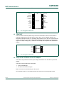
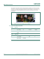
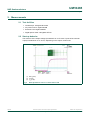
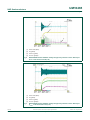
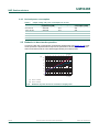
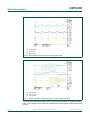
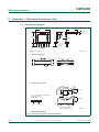
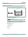
UM10465 TEA1713 and TEA1795 demo board for 150 W all-in-one PC adapter Rev. 1 — 28 September 2011 User manual Document information Info Content Keywords TEA1713T, TEA1795T, 150 W, all-in-one PC adapter, GreenChip-SR, synchronous rectification, LLC, resonant, half-bridge, PFC, controller, converter, burst mode, power supply, demo board Abstract The TEA1713T includes a Power Factor Correction (PFC) controller and a controller for a Half-Bridge resonant Converter (HBC). This user manual describes a 150 W resonant Switching Mode Power Supply (SMPS) for a typical all-in-one PC adapter design based on the TEA1713T and TEA1795T. The board provides an output of 19.5 V/7.7 A. It operates in normal mode for medium and high-power levels and in burst mode for low-power levels. Burst mode operation provides a reduction of power losses to increase performance. The efficiency at high power is well above 90 % and the no load power consumption is well below 500 mW. UM10465 NXP Semiconductors TEA1713 and TEA1795 demo board for 150 W all-in-one PC adapter Revision history Rev Date Description v.1 20110928 first release Contact information For more information, please visit: http://www.nxp.com For sales office addresses, please send an email to: [email protected] UM10465 User manual All information provided in this document is subject to legal disclaimers. Rev. 1 — 28 September 2011 © NXP B.V. 2011. All rights reserved. 2 of 33 UM10465 NXP Semiconductors TEA1713 and TEA1795 demo board for 150 W all-in-one PC adapter 1. Introduction WARNING Lethal voltage and fire ignition hazard The non-insulated high voltages that are present when operating this product, constitute a risk of electric shock, personal injury, death and/or ignition of fire. This product is intended for evaluation purposes only. It shall be operated in a designated test area by personnel qualified according to local requirements and labor laws to work with non-insulated mains voltages and high-voltage circuits. This product shall never be operated unattended. 1.1 Scope of this document This document describes the 150 W all-in-one PC adapter demo board using the TEA1713T and TEA1795T. A functional description is provided, supported by a set of measurements to show the all-in-one PC adapter characteristics. 1.2 TEA1713T The TEA1713T integrates a controller for PFC and a controller for an HBC. It provides the drive function for the discrete MOSFET of the up-converter and for the two discrete power MOSFETs in a resonant half-bridge configuration. The resonant controller part is a high-voltage controller for a Zero Voltage Switching (ZVS) LLC resonant converter. It includes a high-voltage level shift circuit and several protection features such as OverCurrent Protection (OCP), Open-Loop Protection (OLP), Capacitive Mode Protection (CMP) and a general purpose latched protection input. In addition to the resonant controller, the TEA1713T contains a PFC controller. The efficient operation of the PFC is obtained by functions such as quasi-resonant operation at high-power levels and quasi-resonant operation with valley skipping at lower power levels. OCP, OverVoltage Protection (OVP) and demagnetization sensing, ensures safe operation in all conditions. The proprietary high-voltage BCD power logic process makes direct start-up from the rectified universal mains voltage in an efficient way possible. A second low voltage Silicon-On-Insulator (SOI) IC is used for accurate, hi-speed protection functions and control. The combination of PFC and a resonant controller in one IC makes the TEA1713T suitable for all-in-one PC adapters. UM10465 User manual All information provided in this document is subject to legal disclaimers. Rev. 1 — 28 September 2011 © NXP B.V. 2011. All rights reserved. 3 of 33 UM10465 NXP Semiconductors TEA1713 and TEA1795 demo board for 150 W all-in-one PC adapter COMPPFC 1 24 SNSBOOST SNSMAINS 2 23 RCPROT SNSAUXPFC 3 22 SSHBC/EN SNSCURPFC 4 21 SNSFB SNSOUT 5 20 RFMAX SUPIC 6 GATEPFC 7 PGND 8 17 SNSCURHBC SUPREG 9 16 n.c. GATELS 10 15 HB 19 CFMIN TEA1713T 18 SGND 14 SUPHS n.c. 11 13 GATEHS SUPHV 12 014aaa826 Fig 1. Pin configuration TEA1713T 1.3 TEA1795T The TEA1795T GreenChip-SR is a synchronous rectification control IC that needs no external components to tune the timing. Used in all-in-one PC adapter designs, the GreenChip-SR offers a wide VCC operating range between 8.5 V and 38 V, minimizing the number of external components required and enabling simpler designs. In addition, the high driver output voltage (10 V) makes the GreenChip-SR compatible with all MOSFET brands. SSA 1 GND 2 8 SSB 7 VCC TEA1795T GDA 3 6 GDB DSA 4 5 DSB 014aaa976 Fig 2. Pin configuration TEA1795T 1.4 Setup of the 150 W all-in-one PC adapter The board can operate at a mains input voltage of between 90 V and 264 V (universal mains). The demo board contains two subcircuits: • A PFC of BCM-type • An HBC of resonant LLC-type Both converters are controlled by the TEA1713T. At low-power levels, the converters operate in burst mode to reduce power losses. UM10465 User manual All information provided in this document is subject to legal disclaimers. Rev. 1 — 28 September 2011 © NXP B.V. 2011. All rights reserved. 4 of 33 UM10465 NXP Semiconductors TEA1713 and TEA1795 demo board for 150 W all-in-one PC adapter The purpose of the demo board is to demonstrate the operation of the TEA1713T and TEA1795T in a single output supply including burst mode operation. The performance is according today’s general standards and can be used as a starting point for further development. 019aac558 Fig 3. TEA1713T demo board 150 W all-in-one PC adapter 1.5 Input and output properties Table 1. Symbol Description Conditions Specification Unit Vi input voltage AC 90 to 264 V (RMS) fi input frequency - 47 to 60 Hz Pi(no load) no load input power 230 V, 50 Hz < 500 mW Table 2. UM10465 User manual Input data Output data Symbol Description Conditions Specification Unit Vo output voltage - 19.5 V Vo(ripple)(p-p) peak-to-peak ripple voltage 20 MHz bandwidth < 150 mV Io output current continuous 0 to 7.7 A All information provided in this document is subject to legal disclaimers. Rev. 1 — 28 September 2011 © NXP B.V. 2011. All rights reserved. 5 of 33 UM10465 NXP Semiconductors TEA1713 and TEA1795 demo board for 150 W all-in-one PC adapter 2. Measurements 2.1 Test facilities • • • • Oscilloscope: Yokogawa DL1640L AC power source: Agilent 6812B Electronic load: Agilent 6063B Digital power meter: Yokogawa WT210 2.2 Start-up behavior The rise time of the output voltage (measured from 10 % to 90 % point of the nominal output) is between 8 ms to 15 ms, depending on the output current load. (1) (2) (3) 019aac560 (1) HBC (green). (2) IO (blue). (3) VO (purple). Fig 4. UM10465 User manual Start-up behavior at Vmains = 230 V and no load All information provided in this document is subject to legal disclaimers. Rev. 1 — 28 September 2011 © NXP B.V. 2011. All rights reserved. 6 of 33 UM10465 NXP Semiconductors TEA1713 and TEA1795 demo board for 150 W all-in-one PC adapter (1) (2) (3) 019aac563 (1) HBC (green). (2) IO (blue). (3) VO (purple). Fig 5. Start-up behavior at Vmains = 100 V and full load 2.3 Protection levels on SNSCURHBC and SNSOUT during start-up During start-up the voltage at pin RCPROT (protection timer) always rises. SNSCURHBC detects the initial high primary current and SNSOUT starts at a low voltage. After the first switching cycles the levels become normal for operation and the charging of RCPROT ends. The voltage level on RCPROT now decreases to zero again by the external discharge resistor that is part of the RCPROT system. During normal start-up the initial charging of RCPROT must not trigger a protection (4 V level). UM10465 User manual All information provided in this document is subject to legal disclaimers. Rev. 1 — 28 September 2011 © NXP B.V. 2011. All rights reserved. 7 of 33 UM10465 NXP Semiconductors TEA1713 and TEA1795 demo board for 150 W all-in-one PC adapter (1) (2) (3) (4) 019aac564 (1) VSNSCURHBC (blue). (2) VO (yellow). (3) VSNSOUT (green). (4) VRCPROT (purple). Fig 6. SNSCURHBC and/or SNSOUT initially charges the protection timer. Start-up at Vmains = 230 V and no-load (0 A) 019aac565 (1) VSNSCURHBC (blue). (2) VO (yellow). (3) VSNSOUT (green). (4) VRCPROT (purple). Fig 7. UM10465 User manual SNSCURHBC and/or SNSOUT initially charges the protection timer. Start-up at Vmains = 100 V and full load (7.7 A) All information provided in this document is subject to legal disclaimers. Rev. 1 — 28 September 2011 © NXP B.V. 2011. All rights reserved. 8 of 33 UM10465 NXP Semiconductors TEA1713 and TEA1795 demo board for 150 W all-in-one PC adapter 2.4 Efficiency 2.4.1 Efficiency characteristics Efficiency measurements were made measuring the output voltage on the board (not taking into account the losses in an output connection cable). Table 3. Efficiency results Conditions Energy star 2.0 Efficiency (%) efficiency Average 25 % load 50 % load requirement (%) 75 % load 100 % load 100 V, 60 Hz > 87 91.2 89.1 91.4 92.1 92.3 230 V, 50 Hz > 87 92.2 89.3 92.6 93.2 93.6 019aac566 100 η (%) 80 (1) (2) 60 40 20 0 0 30 60 90 120 150 Po (W) (1) Input of 230 V (2) Input 100 V Fig 8. Efficiency at an input voltage of 100 V and 230 V 2.4.2 Power Factor Correction (PFC) Table 4. UM10465 User manual Power Factor correction (PFC) Condition Energy Star 2.0 requirement Output power (W) Power factor 90 V, 60 Hz - 150 0.99 100 V, 60 Hz - 150 0.99 115 V, 60 Hz 0.9 150 0.99 230 V, 50 Hz - 150 0.95 264 V, 50 Hz - 150 0.92 All information provided in this document is subject to legal disclaimers. Rev. 1 — 28 September 2011 © NXP B.V. 2011. All rights reserved. 9 of 33 UM10465 NXP Semiconductors TEA1713 and TEA1795 demo board for 150 W all-in-one PC adapter 2.4.3 No-load power consumption Table 5. Output voltage and power consumption at no-load Condition Energy Star 2.0 requirement (mW) Output voltage (V) No load power consumption (mW) 90 V, 60 Hz 500 mW 19.5 220 100 V, 60 Hz 500 mW 19.5 230 115 V, 60 Hz 500 mW 19.5 240 230 V, 50 Hz 500 mW 19.5 250 264 V, 50 Hz 500 mW 19.5 260 2.5 Behavior in burst mode operation In order to reach the no load power consumption requirements (seeSection 2.4.3), burst mode operation is implemented to improve the performance at low output load. For the demo board burst mode is active below approximately 5 W output power. 019aac567 14 Pin-Po (W) 12 10 8 (1) (2) 6 4 2 0 0 30 60 90 120 150 Po (W) (1) Vmains = 100 V (2) Vmains = 230 V Fig 9. UM10465 User manual Reduction of power losses as a function of output power All information provided in this document is subject to legal disclaimers. Rev. 1 — 28 September 2011 © NXP B.V. 2011. All rights reserved. 10 of 33 UM10465 NXP Semiconductors TEA1713 and TEA1795 demo board for 150 W all-in-one PC adapter (1) (2) (3) 019aac568 (1) VSNSFB (blue). (2) VO (purple). (3) HBC (yellow). Fig 10. Burst mode operation at Vmains = 230 V and no-load (1) (2) (3) 019aac569 (1) HBC (green). (2) VSNSOUT (blue). (3) PFC (yellow). Fig 11. Switch on/off PFC and HBC by VSNSOUT in burst mode operation The interruptive character of burst mode can lead to the generation of unwanted audible noise. As the supply in burst mode only operates at low-power levels, audible noise levels are low. UM10465 User manual All information provided in this document is subject to legal disclaimers. Rev. 1 — 28 September 2011 © NXP B.V. 2011. All rights reserved. 11 of 33 UM10465 NXP Semiconductors TEA1713 and TEA1795 demo board for 150 W all-in-one PC adapter 2.6 Transient response Normal load transients lead to a ripple on the output voltage of < 800 mV. (1) (2) 019aac570 (1) IO (blue) (2) VO (purple) Fig 12. Load-step behavior; typical load-step from zero to full load 2.7 Output ripple voltage and noise Ripple and noise are measured at full output load, buffered with a 10 F capacitor in parallel with a high-frequency 0.1 F capacitor. The varying input voltage of the resonant converter causes a frequency component in the output ripple voltage that is related to the mains voltage frequency: 50 Hz or 60 Hz. The switching frequency of the resonant converter causes the other component in the output ripple voltage. Table 6. UM10465 User manual Ripple and noise test results Mains voltage Mains frequency Output power Ripple frequency Voltage ripple 90 V to 264 V 50 Hz or 60 Hz 150 W 50 Hz or 60 Hz 52 mV (p-p) 90 V to 264 V 50 Hz or 60 Hz 150 W 215 kHz 68 mV (p-p) All information provided in this document is subject to legal disclaimers. Rev. 1 — 28 September 2011 © NXP B.V. 2011. All rights reserved. 12 of 33 UM10465 NXP Semiconductors TEA1713 and TEA1795 demo board for 150 W all-in-one PC adapter (1) (2) (3) 019aac571 (1) VO (yellow). (2) VO(ripple)(p-p) (purple). (3) IO (blue). Fig 13. Output voltage ripple at full load (2 ms/div scale) (1) (2) (3) 019aac572 (1) VO (yellow). (2) VO(ripple)(p-p) (purple). (3) IO (blue). Fig 14. Output voltage ripple at full load (20 s/div scale) UM10465 User manual All information provided in this document is subject to legal disclaimers. Rev. 1 — 28 September 2011 © NXP B.V. 2011. All rights reserved. 13 of 33 UM10465 NXP Semiconductors TEA1713 and TEA1795 demo board for 150 W all-in-one PC adapter 2.8 OverPower Protection (OPP) Tested with a higher current (dynamic overload) on the output voltage, the OPP is activated when the current exceeds 10 A (195 W). This corresponds to a load condition that is 30 % higher than the rated power for continuous use. The OPP is detected by the SNSCURHBC function of the TEA1713T that monitors the primary resonant current. When the voltage on the SNSCURHBC pin exceeds 0.5 V (or 0.5 V) the protection timer is started. (1) (2) (3) 019aac573 (1) VSNSCURHBC (purple). (2) IO (blue). (3) VRCPROT (yellow). Fig 15. Dynamic current load leading to OPP 2.9 Hold-up time The output is set to full load and the mains supply voltage of 100 V is disconnected. The time that passes before the output voltage falls below 90 % of its initial value is then measured. The hold-up time is 39 ms. UM10465 User manual All information provided in this document is subject to legal disclaimers. Rev. 1 — 28 September 2011 © NXP B.V. 2011. All rights reserved. 14 of 33 UM10465 NXP Semiconductors TEA1713 and TEA1795 demo board for 150 W all-in-one PC adapter (1) (2) (3) 019aac574 (1) IO (blue). (2) VO (purple). (3) Vmains (green and yellow). Fig 16. Hold-up time 2.10 Short-circuit protection A short circuit on the output of the resonant converter causes the primary current to increase. This is detected by the SNSCURHBC function leading to running on maximum frequency until the protection timer RCPROT reaches its protection level (4 V). The RCPROT function performs its restart timer function and restarts again when the voltage has dropped to 0.5 V. When the short-circuit is removed, the converter starts up and operates as normal. This is the main protection mechanism. Under certain conditions, other protections can be activated during the output short circuit test. UM10465 User manual All information provided in this document is subject to legal disclaimers. Rev. 1 — 28 September 2011 © NXP B.V. 2011. All rights reserved. 15 of 33 UM10465 NXP Semiconductors TEA1713 and TEA1795 demo board for 150 W all-in-one PC adapter (1) (2) (3) (4) 019aac575 (1) VSNSCURHBC (purple) (2) VRCPROT (yellow) (3) IO (blue) (4) VO (green) Fig 17. Protection and restart at output short-circuit 2.11 Resonant current measurements (1) (2) (3) (4) 019aac576 (1) Iresonant_primary (blue) (2) VCFMIN (yellow) (3) VHB (green) (4) VGATE_MOSFET_LS (purple) Fig 18. Resonant current (full load Io = 7.7 A) UM10465 User manual All information provided in this document is subject to legal disclaimers. Rev. 1 — 28 September 2011 © NXP B.V. 2011. All rights reserved. 16 of 33 UM10465 NXP Semiconductors TEA1713 and TEA1795 demo board for 150 W all-in-one PC adapter (1) (2) (3) (4) 019aac577 (1) Iresonant_primary (blue). (2) VCFMIN (yellow). (3) VHB (green). (4) VGATE_MOSFET_LS (purple). Fig 19. Resonant current (low load Io = 0.5 A) (1) (2) (3) (4) 019aac578 (1) Iresonant_primary (blue). (2) VCFMIN (yellow). (3) VHB (green). (4) VGATE_MOSFET_LS (purple). Fig 20. Resonant current (no-load Io = 0 A) UM10465 User manual All information provided in this document is subject to legal disclaimers. Rev. 1 — 28 September 2011 © NXP B.V. 2011. All rights reserved. 17 of 33 UM10465 NXP Semiconductors TEA1713 and TEA1795 demo board for 150 W all-in-one PC adapter 2.12 Synchronous Rectification The TEA1795T IC is used for synchronous rectification and replaces the rectifier diodes at the secondary side of the resonant adapter. (1) VDRAIN (purple) (2) VGATE (blue) (3) Iresonant_secundary (red) Fig 21. Resonant, switching and secondary currents at nominal output UM10465 User manual All information provided in this document is subject to legal disclaimers. Rev. 1 — 28 September 2011 © NXP B.V. 2011. All rights reserved. 18 of 33 xxxx xxxxxxxxxxxxxxxxxxxxxxxxxxxxxx x xxxxxxxxxxxxxx xxxxxxxxxx xxx xxxxxx xxxxxxxxxxxxxxxxxxxxxxx xxxxxxxxxxxxxxxxxxxxxx xxxxx xxxxxx xx xxxxxxxxxxxxxxxxxxxxxxxxxxxxx xxxxxxxxxxxxxxxxxxxxxx xxxxxxxxxxx xxxxxxx xxxxxxxxxxxxxxxxxxx xxxxxxxxxxxxxxxx xxxxxxxxxxxxxx xxxxxx xx xxxxxxxxxxxxxxxxxxxxxxxxxxxxxxxx xxxxxxxxxxxxxxxxxxxxxxxx xxxxxxx xxxxxxxxxxxxxxxxxxxxxxxxxxxxxxxxxxxxxxxxxxxxxx xxxxxxxxxxx xxxxx x x L101 C103 0.47 μF L 1N5408 BD101 GBU408 L102 L104 PQ2625 315 μH 3 1 L103 D102 Vbulk_cap 6 R102 1.5 MΩ 1206 5 BYV29X-600 Q101 60R199CP TO-220 N SG FG inlet C101 220 pF (400 V) PG C102 220 pF (400 V) BC101 R107 C104 0.68 μF (450 V) C105 1 μF (450 V) D103 NC 0805 NC SOD123 R109 2.2 Ω 0805 PG Q102 PMBT4403 R110 0.05 Ω (2 W) 2512 C107 4.7 nF (25 V) 0603 R114 64.9 kΩ 0603 PG R117 12 kΩ 0603 R115 0Ω 1206 IC101 (PART) TEA1713 (PART) SO-24 GATEPFC SNSAUXPFC R103 SNSMAINS 523 kΩ 1206 PGND C108 2.2 μF (16 V) 1206 7 4 3 24 2 12 8 1 R116 2.2 kΩ 0603 SNSCURPFC C113 NC 0603 SNSBOOST PG SUPHV R118 COMPPFC C108-1 2.2 μF (16 V) 1206 19 of 33 © NXP B.V. 2011. All rights reserved. Fig 22. Circuit diagram TEA1713T 150 W demo board (PFC part) C111 150 nF (25 V) 0603 PG PG 33 kΩ 0603 C112 470 nF (25 V) 0603 019aac579 UM10465 PG C110-1 NC 1206 R114-1 3 MΩ 0603 SG C109 47 nF (25 V) 0603 R104 40.2 kΩ 0603 C110 180 μF (420 V) R113 3.3 MΩ 1206 3 R108 R106 NC 0603 R112 3.3 MΩ 1206 C106 100 pF (630 V) 1206 1 10 Ω 0805 R105 5.1 kΩ 0603 C105-1 NC 1206 2 TEA1713 and TEA1795 demo board for 150 W all-in-one PC adapter Rev. 1 — 28 September 2011 All information provided in this document is subject to legal disclaimers. C104-1 NC 1206 R111 3.3 MΩ 1206 4 NXP Semiconductors R101 1.5 MΩ 1206 3. Circuit diagram UM10465 User manual D101 F101 3.15 A (250 V) xxxxxxxxxxxxxxxxxxxxx xxxxxxxxxxxxxxxxxxxxxxxxxx xxxxxxx x x x xxxxxxxxxxxxxxxxxxxxxxxxxxxxxx xxxxxxxxxxxxxxxxxxx xx xx xxxxx xxxxxxxxxxxxxxxxxxxxxxxxxxx xxxxxxxxxxxxxxxxxxx xxxxxx xxxxxxxxxxxxxxxxxxxxxxxxxxxxxxxxxxx xxxxxxxxxxxx x x xxxxxxxxxxxxxxxxxxxxx xxxxxxxxxxxxxxxxxxxxxxxxxxxxxx xxxxx xxxxxxxxxxxxxxxxxxxxxxxxxxxxxxxxxxxxxxxxxxxxxxxxxx xxxxxxxx xxxxxxxxxxxxxxxxxxxxxxxxx xxxxxxxxxxxxxxxxxxxx xxx NXP Semiconductors UM10465 User manual Vbulk_cap D201 R202 NC NC 0805 SOD123 R201 10 Ω 0805 Q201 2SK3569 TO-220 2 Q301 PSMN7R6-60PS TO-220 C201 NC 1206 1 R203 NC 1206 R301 C301 NC 1206 NC 1206 2 3 3 Vout 1 4 L201 6 D202 R205 NC NC 0805 SOD123 R204 10 Ω 0805 Q202 2SK3569 TO-220 T1 2 C202 NC 1206 1 R206 NC 1206 R303 NC 0805 C315 NC 0603 9 1 DSA D206 ES1J SMA C211 470 pF (1 kV) 1206 2 IC301 5 0.33 μF (25 V) 0805 SUPHS C214 HB R214 n.c. D209 1 kΩ SNSCURHBC BAV99 0603 C215 SGND SOT23 R228 R216 SG CFMIN 0Ω 270 pF 1206 18.2 kΩ SG (25 V) RFMAX 0603 0603 SG SG SNSFB C218 4.7 nF (25 V) 0603 C216 0.22 μF (25 V) 0805 SG 13 12 14 11 15 10 16 9 17 8 2 2.2 nF (25 V) 1206 NC 1206 SUPREG GATELS C219 0.1 μF (25 V) 0603 SUPREG PGND C204 10 μF (50 V) C205 0.1 μF (50 V) 0603 C203 220 μF (50 V) Q206 NC SOT-23 1 kΩ 0603 4 6 R315 NC 0603 3 2 R211 100 kΩ 0603 RT210 100 kΩ C222 10 nF (25 V) 0603 R223 2 kΩ 0603 R212 294 kΩ 0603 SG Q205 NC SOT-23 N-INV1 INV1 SG Fig 23. Circuit diagram TEA1713T 150 W demo board (HBC part) 3 7 5 2 LM293 SO-8 6 8 4 C312 OUT1 OUT2 1 INV1 1 3 2 8 GND R310 4.53 kΩ 0603 R310-1 294 kΩ 0603 R313 191 Ω 0603 R313-1 NC 0603 N-INV1 N-INV2 5 AP4310A 7 4 IC303 6 INV2 VCC C310 IC305 LTV817A 3 R219 1 kΩ 0603 SUPREG Vcc+ C220 10 nF (25 V) 0603 Vcc- 100 kΩ 0603 NC 0603 SUPREG SG IC201 10 kΩ 0603 SG C225 NC 0603 249 kΩ 0603 1 R312 4 C213 10 pF (50 V) 0603 R217 OUT2 SUPREG SG R218 2.2 kΩ 0603 OUT1 R225 C311 0.1 μF (25 V) 0603 ES1B SMA R311 300 kΩ 0603 R220 392 kΩ 0603 C221 1 nF (25 V) 0603 N-INV2 INV2 R221 100 kΩ 0603 2 C223 0.1 F (25 V) 1206 R317 51 kΩ 0603 C313 1 nF (25 V) 0603 0.1 μF (25 V) 0603 C401 680 pF SG SG 019aac580 UM10465 20 of 33 © NXP B.V. 2011. All rights reserved. C224 NC 0603 PG R309 30.9 kΩ 0603 C314 NC 0603 R316 D204 5 PG R318 NC 0603 1 IC304 LTV817A PG SUPREG R208 BAS16H SOD123 SG NC 0603 C227 NC 0603 SG R308 10 kΩ 0603 R314 4 R209 40.2 kΩ 0603 33 kΩ 0603 SG C309 0.1 μF (25 V) 0603 GATEPFC 1 ZD201 NC SOT-23 GND D203 n.c. C308 NC 0603 R307 0.012 Ω 2W 2512 ES1B SMA R208 332 kΩ 0603 C307 820 μF (25 V) 3 NC 1206 SUPHV C306 820 μF (25 V) C305 820 μF (25 V) Q302 PSMN7R6-60PS TO-220 C302 R222 3 C304 0.1 μF (50 V) 0603 GND SSB 1 R304 IC101 C217 2.2 μF (25 V) 0805 Vcc R305 4.7 Ω 0805 C212 SUPREG R216 150 kΩ 0603 8 2 GDB R306 1 kΩ 0805 22 nF (600 V) 18 TEA1713T 7 PG SUPIC SO-24 19 6 SNSOUT 20 5 C210 SNSCURPFC 21 4 10 nF SSHBC/EN SNSAUXPFC (25 V) 22 3 1206 PCPROT SNSMAINS 23 2 SG SNSBOOST COMPPFC 24 1 SG 6 DSB 12 R213 10 Ω 1206 GATEHS 7 TEA1713 and TEA1795 demo board for 150 W all-in-one PC adapter Rev. 1 — 28 September 2011 All information provided in this document is subject to legal disclaimers. SG R210 1 SO-8 C200 12.4 Ω 1206 SSA 3 FLY1 C316 NC 0603 SUPREG GDA 4 TEA1795 3 PG R302 4.7 Ω 0805 xxxxxxxxxxxxxxxxxxxxx xxxxxxxxxxxxxxxxxxxxxxxxxx xxxxxxx x x x xxxxxxxxxxxxxxxxxxxxxxxxxxxxxx xxxxxxxxxxxxxxxxxxx xx xx xxxxx xxxxxxxxxxxxxxxxxxxxxxxxxxx xxxxxxxxxxxxxxxxxxx xxxxxx xxxxxxxxxxxxxxxxxxxxxxxxxxxxxxxxxxx xxxxxxxxxxxx x x xxxxxxxxxxxxxxxxxxxxx xxxxxxxxxxxxxxxxxxxxxxxxxxxxxx xxxxx xxxxxxxxxxxxxxxxxxxxxxxxxxxxxxxxxxxxxxxxxxxxxxxxxx xxxxxxxx xxxxxxxxxxxxxxxxxxxxxxxxx xxxxxxxxxxxxxxxxxxxx xxx NXP Semiconductors UM10465 User manual Vbulk_cap disabling OCP function (OCP remains) D201 R202 n.c. SOD123 n.c. 0805 Q201 2SK3569 TO-220 R201 R202 Vout GDA 4 SSA 3 1 C202 n.c. 1206 2 7 FLY1 bootstrap function for high side driver supply 2 5 R210 12.4 Ω 1206 6 DSB 12 C316 n.c. 0603 R306 1 kΩ 0805 C211 optional circuit to optimize SR switching 2.2 nF 25 V 1206 C304 0.1 μF 50 V 0603 C305 820 μF 25 V SSB R305 4.7 Ω 0805 Q302 1 PSMN7R6-60PS TO-220 C307 820 μF 25 V C306 820 μF 25 V C308 n.c. 0603 TEA1795 syncrec switching R307 3 2 470 pF 1 kV 1206 GND 8 GDB 22 nF 600 V PG C212 SG IC301 TEA1795 SO-8 3 VCC GND R304 C302 n.c. 1206 n.c. 1206 C309 0.1 μF 25 V 0603 output voltage sensing and regulation by error amplifier and optocoupler 0.012 Ω 2W 2512 R308 10 kΩ 0603 R314 oscillator and frequency range preset R215 18.2 kΩ 0603 SUPHS HB n.c. R214 1 kΩ C215 0603 SNSCURHCB SGND SG 270 pF 25 V SG 0603 SG GATEHS C214 0.33 μF 25 V 0805 CFMIN RFMAX SNSFB SSHBC/EN PCPROT C217 2.2 μF 25 V 0805 R216 150 kΩ 0603 SNSBOOST 13 12 14 11 15 10 16 9 17 8 18 7 19 6 20 5 21 4 22 3 23 2 24 1 SUPHV n.c. SUPREG PGND 21 of 33 © NXP B.V. 2011. All rights reserved. SG softstart time preset C204 10 μF 50 V R209 40.2 kΩ 0603 SNSCURPFC SNSMAINS COMPPFC D208 BAS16H SOD123 SG timing PFC burst C222 10 nF 25 V 0603 Q206 n.c. SOT-23 1 RT201 100 kΩ R211 100 kΩ 0603 R223 2 kΩ 0603 R212 294 kΩ 0603 ZD201 n.c. SOT-23 R227 n.c. 0603 C224 n.c. 0603 SG 3 10 kΩ 0603 2 C311 0.1 μF 25 V 0603 SG ES1B SMA C213 10 pF 50 V 0603 C217 SG SUPREG C225 n.c. 0603 249 kΩ 0603 OUT2 R225 SUPREG 33 kΩ 0603 IC201 LM293 SO-8 Fig 24. Circuit diagram TEA1713T 150 W demo board (HBC part) enable burst mode switch N-INV1 3 2 1 8 VCC+ VCC- 75 N-INV2 6 4 INV2 C220 10 nF 25 V 0603 SG 3 Q204 PMBT4401 SOT-23 C221 1 nF 25 V 0603 SG 1 R220 392 kΩ 0603 R221 100 kΩ 0603 R310 4.53 kΩ 0603 n.c. 0603 INV1 1 2 5 7 4 8 6 GND R310-1 294 kΩ 0603 R312 100 kΩ 0603 N-INV1 3 2 IC303 AP4310A IC305 LTV817A R219 1 kΩ 0603 INV1 4 current sensing for eabling burst mode C312 OUT2 SUPREG R311 300 kΩ 0603 R309 n.c. 0603 C314 n.c. 0603 OUT1 R218 2.2 kΩ 0603 burst mode comparator circuit OUT1 Q203 PMBT4401 SOT-23 SG R316 R315 n.c. 0603 5 SG SG Q205 n.c. SOT-23 1 SUPREG n.c. 0603 3 4 PG PG R318 n.c. 0603 IC304 LTV817A PG mesuring output voltage for OVP and UVP C210 10 nF 25 V 1206 SNSAUXPFC 1 kΩ 0603 4 6 C203 220 μF 50 V D204 SG SNSOUT R222 C205 0.1 μF 50 V 0603 PG SUPIC SUPREG D203 ES1B SMA N-INV2 INV2 C313 1 nF 25 V 0603 VCC C310 R313 191 Ω 0603 R313-1 n.c. 0603 0.1 μF 25 V 0603 C401 C223 0.1 μF 25 V 1206 R317 51 kΩ 0603 680 pF aaa-000111 UM10465 SG C218 4.7 nF 25 V 0603 R208 332 kΩ 0603 GATEPFC SG C216 0.22 μF 25 V 0805 C219 0.1 μF 25 V 0603 GATELS IC101 TEA1713T SO-24 preset of RC-timer SUPREG TEA1713 and TEA1795 demo board for 150 W all-in-one PC adapter Rev. 1 — 28 September 2011 All information provided in this document is subject to legal disclaimers. primary current sensing: OCR/OCP R213 10 Ω 1206 R302 4.7 Ω 0805 DSA C315 n.c. 0603 9 2 C200 D206 ES1J SMA 3 R303 1 kΩ 0805 T1 R206 n.c. 1206 optional circuit to optimize SR switching Q301 1 PSMN7R6-60PS TO-220 1 10 Ω 0805 SUPREG n.c. 1206 1 R204 optional compensation of OCR+OCP for input voltage variations C301 n.c. 1206 3 Q202 2SK3569 TO-220 n.c. 0805 n.c. SOD123 R301 2 4 L201 6 R202 SG C201 n.c. 1206 R203 n.c. 1206 optional circuit to limit gate drive current R228 0Ω 1206 2 1 10 Ω 0805 D209 BAV99 SOT23 optional capacitors to optimize transitions xxxxxxxxxxxxxxxxxxxxx xxxxxxxxxxxxxxxxxxxxxxxxxx xxxxxxx x x x xxxxxxxxxxxxxxxxxxxxxxxxxxxxxx xxxxxxxxxxxxxxxxxxx xx xx xxxxx xxxxxxxxxxxxxxxxxxxxxxxxxxx xxxxxxxxxxxxxxxxxxx xxxxxx xxxxxxxxxxxxxxxxxxxxxxxxxxxxxxxxxxx xxxxxxxxxxxx x x xxxxxxxxxxxxxxxxxxxxx xxxxxxxxxxxxxxxxxxxxxxxxxxxxxx xxxxx xxxxxxxxxxxxxxxxxxxxxxxxxxxxxxxxxxxxxxxxxxxxxxxxxx xxxxxxxx xxxxxxxxxxxxxxxxxxxxxxxxx xxxxxxxxxxxxxxxxxxxx xxx 3.15 A 250 V L101 C103 0.47 μF R101 1.5 MΩ 1206 BD101 GBU408 L102 L104 PQ2625 315 μH L103 L 3 R101 1.5 MΩ 1206 N D102 BYV29X-600 Vbulk_cap 1 6 5 Q101 60R199CP TO-220 4 PG mains input filters inlet C101 220 pF 400 V NXP Semiconductors UM10465 User manual D101 1N5408 F101 C102 220 pF 400 V SG C104 0.68 μF 450 V C104-1 n.c. 1206 PG R107 C105-1 n.c. 1206 10 Ω 0805 R105 5.1 kΩ 0603 R108 R109 2.2 Ω 0805 R110 0.05 Ω 2W 2512 Q102 PMBT4403 SG R113 3.3 MΩ 1206 D103 R106 n.c. 0603 C107 4.7 nF 25 V 0603 optional circuit to limit gate drive current coil state sensing R112 3.3 MΩ 1206 C106 100 pF 630 V 1206 3 n.c. n.c. 0805 SOD123 PFC filter 2 BC101 1 R114 64.9 kΩ 0603 C110 180 μF 420 V C110-1 n.c. 1206 R114-1 3 MΩ 0603 PG bus voltage sensing C109 47 nF 25 V 0603 R117 12 kΩ 0603 current sensing and soft-start preset GATEPFC SNSAUXPFC R103 523 kΩ 1206 R104 40.2 kΩ 0603 C108 2.2 μF 16 V 1206 PGND C108-1 2.2 μF 16 V 1206 SG 4 3 24 2 12 8 1 C113 n.c. 0603 SNSBOOST SG SUPHV R118 COMPPFC C111 150 nF 25 V 0603 PG high voltage startup SNSCURPFC SG 33 kΩ 0603 C112 470 nF 25 V 0603 preset of gain compensation for mains voltage aaa-000112 Fig 25. Circuit diagram TEA1713T 150 W demo board (PFC part) UM10465 22 of 33 © NXP B.V. 2011. All rights reserved. sensing mains voltage SNSMAINS 7 R115 0Ω 1206 R116 2.2 kΩ 0603 IC101 (PART) TEA1713 (PART) SO-24 TEA1713 and TEA1795 demo board for 150 W all-in-one PC adapter Rev. 1 — 28 September 2011 All information provided in this document is subject to legal disclaimers. PG C105 1 μF 450 V R111 3.3 MΩ 1206 UM10465 NXP Semiconductors TEA1713 and TEA1795 demo board for 150 W all-in-one PC adapter 4. PCB layout HS1 J16 FG C101 Q101 F101 T3.15A/250V C102 J2 J1 D102 J17 Q201 Q202 BC101 J10 C200 L201 J6 J15 J18 T1 C401 INLET L101 J3 C103 J4 C203 C110 L104 C307 Vout J9 GND C204 J7 J8 C105 APBADC056 D101 J5 C306 RT210 L103 L102 Fly J12 J19 J14 BD101 Ver. A C104 HS2 IC305 J11 IC304 C305 J13 Q302 Q301 HS3 019aac581 Fig 26. Demo board PCB layout (copper tracks and areas) 5. Bill Of Materials (BOM) Table 7 provides detailed component information for the TEA1713T and TEA1795T demo board for 150 W all-in-one PC adapter. Table 7. BOM for the TEA1713T and TEA1795Tdemo board Item Location Quantity Description 1 BC101 1 bead core; axial lead; WBRH3.5*4.7*0.8; 3L 2 BD101 1 bridge diode; GBU408; Lite-On 4 A; 800 V 3 C101; C102 2 ceramic; Y1-capacitor; KX/Murata 220 pF; 250 V (AC) 4 C103 1 MKP/HJC; X-capacitor; 0.47 F; 275 V (AC) 5 C104 1 MPPN/HJC; radial lead 680 nF; 450 V (DC) 6 C105 1 MPPN/HJC; radial lead 1 F; 450 V (DC) 7 C106 1 MLCC; SMD 1206; NPO; 100 pF; 630 V 8 C107; C218 2 MLCC; SMD 0603; X7R; 4.7 nF; 25 V 9 C108; C108-1 2 MLCC; SMD 1206; X7R; 2.2 F; 16 V 10 C109 1 MLCC; SMD 0603; X7R; 47 nF; 25 V 11 C110 1 electrolytic capacitor; NCC; 180 F/420 V; KMQ (W 30 mm H 25 mm) 12 C111 1 MLCC; SMD 0603; X7R; 150 nF; 25 V 13 C112 1 MLCC; SMD 0603; X7R; 470 nF; 25 V 14 C200 1 MP3/HJC; radial lead 22 nF; 600 V 15 C203 1 E/C; radial lead; 105 C; 10 16 mm; KY/NCC 220 F; 50 V 16 C204 1 E/C; radial lead; 105 C; 5 11 mm; KY/NCC 10 F; 50 V UM10465 User manual All information provided in this document is subject to legal disclaimers. Rev. 1 — 28 September 2011 © NXP B.V. 2011. All rights reserved. 23 of 33 UM10465 NXP Semiconductors TEA1713 and TEA1795 demo board for 150 W all-in-one PC adapter Table 7. BOM for the TEA1713T and TEA1795Tdemo board …continued Item Location Quantity Description 17 C205; C304 2 MLCC; SMD 0603; X7R; 100 nF; 50 V 18 C210 1 MLCC; SMD 1206; X7R; 10 nF; 25 V 19 C211 1 MLCC; SMD 1206; NPO; 470 pF; 1 kV 20 C212 1 MLCC; SMD 1206; X7R; 2.2 nF; 25 V 21 C213 1 MLCC; SMD 0603; X7R; 10 pF; 50 V 22 C214 1 MLCC; SMD 0805; X7R; 330 nF; 25 V 23 C215 1 MLCC; SMD 0603; X7R; 270 pF; 25 V 24 C216 1 MLCC; SMD 0805; X7R; 220 nF; 25 V 25 C217 1 MLCC; SMD 0805; X7R; 2.2 F; 25 V 26 C219; C309; C310; C311 4 MLCC; SMD 0603; X7R; 100 nF; 25 V 27 C220; C222 2 MLCC; SMD 0603; X7R; 10 nF; 25 V 28 C221; C313 2 MLCC; SMD 0603; X7R; 1 nF; 25 V 29 C223 1 MLCC; SMD 1206; X7R; 100 nF; 25 V 30 C305; C306; C307 3 electrolytic capacitor; NCC; 820 F; 25 V; KZH (W 10 mm H 20 mm) 31 C401 1 ceramic; Y1-capacitor; KX/Murata; 680 pF; 250 V (AC) 32 D101 1 general purpose diode; NXP Semiconductors; 1N5408; 3 A; 1 KV 33 D102 1 ultrafast power diode; BYV29X-600 34 D203; D204 2 ultrafast rectifier; SMA; ES1B; 1 A; 100 V 35 D206 1 ultrafast rectifier; SMA; ES1J; 1 A; 600 V 36 D208 1 high speed switching diode; SOD123F; BAS16H; 100 V 37 D209 1 high speed double diode; SOT23; BAV99; 75 V 38 F101 1 fuse; MST(CONQUER); 3.15 A; 250 V 39 IC101 1 resonant power supply control IC with PFC; NXP Semiconductors; SO24; TEA1713T 40 IC201 1 low power dual voltage comparator; SO8; LM293 41 IC301 1 GreenChip synchronous rectifier controller; SO8; TEA1795T; NXP Semiconductors 42 IC303 1 dual opamp and voltage reference; SO8; AP4310A; BCD 43 IC304; IC305 2 high density mounting type photocoupler; DIP 4; LTV817A; LiteOn 44 Inlet 1 AC inlet 3P 45 L101 1 EMI choke; 7.35 mH; SA382/HJC 46 L102 1 EMI choke; 11.07 mH; SA383/HJC 47 L103 1 filter choke 170 H; SA384/HJC 48 L104 1 PFC choke; PQ2625/315uH; SA136/HJC 49 L201 1 choke; ATQ2116.8/44 H; SA135/HJC 50 T1 1 XFMR; PQ3221/800uH; SA137/HJC 51 Q101 1 MOSFET; IPA60R199CP; TO220; Infineon; 16 A; 600 V 52 Q102 1 PNP switching transistor; PMBT4403; SOT23; NXP Semiconductors 53 Q201; Q202 2 MOSFET; 2SK3569; TO220; Toshiba; 10 A; 600 V 54 Q203; Q204 2 NPN switching transistor; SOT23; NXP Semiconductors; PMBT4401 55 Q301; Q302 2 MOSFET; PSMN7R6-60PS; TO220AB; NXP Semiconductors; 92 A; 60 V UM10465 User manual All information provided in this document is subject to legal disclaimers. Rev. 1 — 28 September 2011 © NXP B.V. 2011. All rights reserved. 24 of 33 UM10465 NXP Semiconductors TEA1713 and TEA1795 demo board for 150 W all-in-one PC adapter Table 7. BOM for the TEA1713T and TEA1795Tdemo board …continued Item Location Quantity Description 56 R101; R102 2 resistor; SMD 1206; thin film; 1.5 M; 5 % 57 R103 1 resistor; SMD 1206; thin film; 523 k; 1 % 58 R104 1 resistor; SMD 0603; thin film; 40.2 k; 1% 59 R105 1 resistor; SMD 0603; thin film; 5.1 k; 1 % 60 R107; R201; R204 3 resistor; SMD 0805; thin film; 10 ; 5 % 61 R109 1 resistor; SMD 0805; thin film; 2.2 ; 5 % 62 R110 1 resistor; SMD 2512/2W RLP; thin film; 0.05 ; 1 %; TAI 63 R111; R112; R113 3 Resistor; SMD 1206; thin film; 3.3 M; 1 % 64 R114 1 resistor; SMD 0603; thin film; 64.9 k; 1 % 65 R114-1 1 resistor; SMD 0603; thin film; 3 M; 1 % 66 R115; RJ1; RJ2; RJ3; RJ4; 17 RJ5; RJ6; RJ7; RJ8; RJ9; RJ10; RJ11; RJ12; RJ13; RJ14; RJ15; R228 resistor; SMD 1206; thin film; 0 ; 5 % 67 R214; R219; R314 3 resistor; SMD 0603; thin film; 1 K; 1 % 68 R117 1 resistor; SMD 0603; thin film; 12 k; 5 % 69 R118; R225 2 resistor; SMD 0603; thin film; 33 k; 5 % 70 R208 1 resistor; SMD 0603; thin film; 332 k; 1 % 71 R209 1 resistor; SMD 0603; thin film; 40.2 k; 1 % 72 R210 1 resistor; SMD 1206; thin film; 12.4 ; 1 % 73 R213 1 resistor; SMD 1206; thin film; 10 m; 1 % 74 R211; R221; R312 3 resistor; SMD 0603; thin film; 100 k; 1 % 75 R212 1 resistor; SMD 0603; thin film; 294 k; 1 % 76 R215 1 resistor; SMD 0603; thin film; 18.2 k; 1 % 77 R216 1 resistor; SMD 0603; thin film; 150 k; 1 % 78 R217 1 resistor; SMD 0603; thin film; 249 k; 1 % 79 R116; R218 2 resistor; SMD 0603; thin film; 2.2 k; 5 % 80 R220 1 resistor; SMD 0603; thin film; 392 k; 1% 81 R223 1 resistor; SMD 0603; thin film; 2 k; 1 % 82 R308; R316 2 resistor; SMD 0603; thin film; 10 k; 1% 83 RT201 1 NTC thermistor; TTC3A104F4192EY; Thinking; 100 k; 1% 84 R302; R305 2 resistor; SMD 0805; thin film; 4.7 ; 5 % 85 R303; R306 2 resistor; SMD 0805; thin film; 1 k; 1 % 86 R307 1 resistor; SMD 2512/2W RLP; TAI; thin film; 12 m; 1 % 87 R309 1 resistor; SMD 0603; thin film; 30.9 k; 1 % 88 R310 1 resistor; SMD 0603; thin film; 4.53 k; 1 % 89 R310-1 1 resistor; SMD 0603; thin film; 294 k; 1 % 90 R311 1 resistor; SMD 0603; thin film; 300 k; 1 % 91 R313 1 resistor; SMD 0603; thin film; 191 ; 1 % 92 R317 1 resistor; SMD 0603; thin film; 51 k; 1 % UM10465 User manual All information provided in this document is subject to legal disclaimers. Rev. 1 — 28 September 2011 © NXP B.V. 2011. All rights reserved. 25 of 33 UM10465 NXP Semiconductors TEA1713 and TEA1795 demo board for 150 W all-in-one PC adapter Table 7. BOM for the TEA1713T and TEA1795Tdemo board …continued Item Location Quantity Description 93 HS1 1 heatsink-HS1 for Q101; D102; Q201; Q202 94 HS2 1 heatsink-HS2; for BD101 95 HS3 1 heatsink-HS3; for Q301; Q302 UM10465 User manual All information provided in this document is subject to legal disclaimers. Rev. 1 — 28 September 2011 © NXP B.V. 2011. All rights reserved. 26 of 33 UM10465 NXP Semiconductors TEA1713 and TEA1795 demo board for 150 W all-in-one PC adapter 6. Appendix 1 - Resonant transformer data 6.1 Transformer diagram 35.5 max. 18 ± 2.0 2.5 max. 4 ± 0.5 24 max. tape 3.5 ± 0.5 1 6 6 0.8 ± 0.1 7 core add epoxy dimensions in mm aaa-000104 a. Side and end views 7.6 ± 0.5 1 6 12 7 HJC-SA137D HJC xxxx 30.5 ± 0.5 36 max 12 7 dimensions in mm 1 6 5 ± 0.3 aaa-000105 b. Bottom and top views 8.0 min 1. pin 7,10 cut off. pin 8,11 cut off 2/3 2. gap core on top. 3. date code. YEAR 10.0 min WEEK yellow mylar tape at pin 7 & 12 bottom side aaa-000106 c. Mounting instructions Fig 27. Resonant transformer data: HJC-SA137D UM10465 User manual All information provided in this document is subject to legal disclaimers. Rev. 1 — 28 September 2011 © NXP B.V. 2011. All rights reserved. 27 of 33 UM10465 NXP Semiconductors TEA1713 and TEA1795 demo board for 150 W all-in-one PC adapter winding construction: instruction tape: 1 mil tape pin top 2 Ts N9 (6 -5) 2UEW 0.2 x 1 N8 (4 -6) 2UEW 0.2 x 1 4 Ts 4 Ts spaced winding N7 (FLY1 -9) TEX-ELZ 0.2 / 7 N7 (12 - FLY1) TEX-ELZ 0.2 / 7 3 Ts 3 Ts closed winding N5 (FLY1 -9) TEX-ELZ 0.3 / 7 N4 (12 - FLY1) TEX-ELZ 0.3 / 7 3 Ts 3 Ts closed winding N3 (FLY1 -9) TEX-ELZ 0.3 / 7 N2 (12 - FLY1) TEX-ELZ 0.3 / 7 3 Ts 3 Ts closed winding 1T 1T teflon tube 1T 1 N1 2 12 N2,N4,N6 4 1T Fly1 N8 N3,N5,N7 6 N9 9 closed winding 5 E1 copper foil 1 mil x 6 mm(w) leadwire dia 0.3 to pin 6 1.1 Ts 1T N1 (1 -2) Litz 0.1 / 30 copper foil 6 E1 primary 31 Ts closed winding bobbin secondary aaa-000107 margin tape 1.5 mm Fig 28. Transformer schematic diagram and winding overview 6.2 Transformer electrical specification Table 8. Electrical specification See Table note 1, Table note 2 and Table note 3 for the relevant measuring conditions. Parameter Start Finish Specification Inductance[1] 1 2 800 H; 3 % Leakage inductance[1] 1 1 sec short; 15 H maximum DC resistance[2] 1 2 165 m maximum 4 5 490 m maximum Voltage ratio[3]; input 1, 2 UM10465 User manual 12 fly1 6.10 m maximum 4 5 2.58 V (RMS) 0.08 V (RMS) 12 fly1 0.975 V (RMS) 0.08 V (RMS) fly1 9 0.975 V (RMS) 0.08 V (RMS) [1] Measured with HP: 4284A LCR meter (or equivalent), f = 100 kHz, V = 1 V (RMS) at 25 C. [2] Measured with CHEN HWA 502 AC meter (or equivalent) at 25 C. [3] Measured with CHEN HWA 310 meter (or equivalent); 20 kHz, 10 V (RMS). All information provided in this document is subject to legal disclaimers. Rev. 1 — 28 September 2011 © NXP B.V. 2011. All rights reserved. 28 of 33 UM10465 NXP Semiconductors TEA1713 and TEA1795 demo board for 150 W all-in-one PC adapter 7. Appendix 2 - PFC coil data 7.1 Transformer schematic diagram and winding specification winding construction: instruction tape: 1 mil tape pin side 2 Ts teflon tube N1 (5 -4) 2UEW 0.25 mm x 1 5 3 3 Ts spaced winding 53 Ts closed winding N2 N1 4 1 primary top side 1T secondary N1 (3 -1) Litz 0.1 mm x 55 bobbin aaa-000108 margin tape 3.2 mm 2 Ts Fig 29. Transformer schematic diagram and winding overview 7.2 Transformer electrical specification Table 9. Electrical specification See Table note 1 for the relevant measuring conditions. Parameter Start Finish Specification Inductance[1] 3 1 315 H; 3 % Leakage inductance[1] 3 1 not applicable [1] Measured with HP: 4284A LCR meter (or equivalent), f = 100 kHz, V = 1 V (RMS) at 25 C. 7.3 Core, bobbin and marking Core and bobbin: • Core: PQ2625 (JPP-44A) • Bobbin: PM9820 • Ae: 120 mm2 Marking: • HJC-SA136A UM10465 User manual All information provided in this document is subject to legal disclaimers. Rev. 1 — 28 September 2011 © NXP B.V. 2011. All rights reserved. 29 of 33 UM10465 NXP Semiconductors TEA1713 and TEA1795 demo board for 150 W all-in-one PC adapter 8. Appendix - Choke coil data 8.1 Choke coil schematic diagram and winding specification winding construction: instruction tape: 1 mil tape pin side top side 2 Ts teflon tube 4 N1 N1 (4 -6) Litz 0.1 mm x 30 6 primary closed winding 40 Ts secondary bobbin aaa-000109 Fig 30. Transformer schematic diagram and winding overview 8.2 Transformer electrical specification Table 10. Electrical specification See Table note 1 and Table note 2 or the relevant measuring conditions. Parameter Start Finish Specification Inductance[1] 4 6 44 H; 3 % 3 1 not applicable 4 6 145 M maximum Leakage inductance[1] DC resistance[2] [1] Measured with HP: 4284A LCR meter (or equivalent), f = 100 kHz, V = 1 V (RMS) at 25 C. [2] Measured with CHEN HWA 502 AC meter (or equivalent) at 25 C. 8.3 Core, bobbin and marking Core and bobbin: • Core: ATQ21/16.8 (JPP-44A) • Bobbin: PM9820 Marking: • HJC-SA135 UM10465 User manual All information provided in this document is subject to legal disclaimers. Rev. 1 — 28 September 2011 © NXP B.V. 2011. All rights reserved. 30 of 33 UM10465 NXP Semiconductors TEA1713 and TEA1795 demo board for 150 W all-in-one PC adapter 9. Abbreviations Table 11. Abbreviations Acronym Description BCM Boundary conduction Mode CMP Capacitive Mode Protection EMC ElectroMagnetic Compatibility EMI ElectroMagnetic Interference HBC Half-Bridge resonant Converter MOSFET Metal-Oxide Semiconductor Field-Effect Transistor OCP OverCurrent Protection OPP OverPower Protection OVP OverVoltage Protection OLP Open-Loop Protection PCB Printed-Circuit Board PFC Power Factor Correction SOI Silicon-On-Insulator ZVS Zero Voltage Switching 10. References UM10465 User manual [1] TEA1713T — data sheet - resonant power supply control IC with PFC [2] TEA1795T — data sheet - GreenChip synchronous rectifier [3] AN10881 — application note - resonant power supply control IC with PFC [4] UM10379 — user manual - 250 W LCD-TV demo board [5] UM10450 — user manual - 90 W notebook adaptor demo board [6] Calculation sheet — http://www.nxp.com/technical_support/designportal/llc All information provided in this document is subject to legal disclaimers. Rev. 1 — 28 September 2011 © NXP B.V. 2011. All rights reserved. 31 of 33 UM10465 NXP Semiconductors TEA1713 and TEA1795 demo board for 150 W all-in-one PC adapter 11. Legal information 11.1 Definitions Draft — The document is a draft version only. The content is still under internal review and subject to formal approval, which may result in modifications or additions. NXP Semiconductors does not give any representations or warranties as to the accuracy or completeness of information included herein and shall have no liability for the consequences of use of such information. 11.2 NXP Semiconductors does not accept any liability related to any default, damage, costs or problem which is based on any weakness or default in the customer’s applications or products, or the application or use by customer’s third party customer(s). Customer is responsible for doing all necessary testing for the customer’s applications and products using NXP Semiconductors products in order to avoid a default of the applications and the products or of the application or use by customer’s third party customer(s). NXP does not accept any liability in this respect. Export control — This document as well as the item(s) described herein may be subject to export control regulations. Export might require a prior authorization from competent authorities. Disclaimers Limited warranty and liability — Information in this document is believed to be accurate and reliable. However, NXP Semiconductors does not give any representations or warranties, expressed or implied, as to the accuracy or completeness of such information and shall have no liability for the consequences of use of such information. In no event shall NXP Semiconductors be liable for any indirect, incidental, punitive, special or consequential damages (including - without limitation - lost profits, lost savings, business interruption, costs related to the removal or replacement of any products or rework charges) whether or not such damages are based on tort (including negligence), warranty, breach of contract or any other legal theory. Notwithstanding any damages that customer might incur for any reason whatsoever, NXP Semiconductors’ aggregate and cumulative liability towards customer for the products described herein shall be limited in accordance with the Terms and conditions of commercial sale of NXP Semiconductors. Right to make changes — NXP Semiconductors reserves the right to make changes to information published in this document, including without limitation specifications and product descriptions, at any time and without notice. This document supersedes and replaces all information supplied prior to the publication hereof. Suitability for use — NXP Semiconductors products are not designed, authorized or warranted to be suitable for use in life support, life-critical or safety-critical systems or equipment, nor in applications where failure or malfunction of an NXP Semiconductors product can reasonably be expected to result in personal injury, death or severe property or environmental damage. NXP Semiconductors accepts no liability for inclusion and/or use of NXP Semiconductors products in such equipment or applications and therefore such inclusion and/or use is at the customer’s own risk. Applications — Applications that are described herein for any of these products are for illustrative purposes only. NXP Semiconductors makes no representation or warranty that such applications will be suitable for the specified use without further testing or modification. Customers are responsible for the design and operation of their applications and products using NXP Semiconductors products, and NXP Semiconductors accepts no liability for any assistance with applications or customer product design. It is customer’s sole responsibility to determine whether the NXP Semiconductors product is suitable and fit for the customer’s applications and products planned, as well as for the planned application and use of customer’s third party customer(s). Customers should provide appropriate design and operating safeguards to minimize the risks associated with their applications and products. Safety of high-voltage evaluation products — The non-insulated high voltages that are present when operating this product, constitute a risk of electric shock, personal injury, death and/or ignition of fire. This product is intended for evaluation purposes only. It shall be operated in a designated test area by personnel that is qualified according to local requirements and labor laws to work with non-insulated mains voltages and high-voltage circuits. The product does not comply with IEC 60950 based national or regional safety standards. NXP Semiconductors does not accept any liability for damages incurred due to inappropriate use of this product or related to non-insulated high voltages. Any use of this product is at customer’s own risk and liability. The customer shall fully indemnify and hold harmless NXP Semiconductors from any liability, damages and claims resulting from the use of the product. Evaluation products — This product is provided on an “as is” and “with all faults” basis for evaluation purposes only. NXP Semiconductors, its affiliates and their suppliers expressly disclaim all warranties, whether express, implied or statutory, including but not limited to the implied warranties of non-infringement, merchantability and fitness for a particular purpose. The entire risk as to the quality, or arising out of the use or performance, of this product remains with customer. In no event shall NXP Semiconductors, its affiliates or their suppliers be liable to customer for any special, indirect, consequential, punitive or incidental damages (including without limitation damages for loss of business, business interruption, loss of use, loss of data or information, and the like) arising out the use of or inability to use the product, whether or not based on tort (including negligence), strict liability, breach of contract, breach of warranty or any other theory, even if advised of the possibility of such damages. Notwithstanding any damages that customer might incur for any reason whatsoever (including without limitation, all damages referenced above and all direct or general damages), the entire liability of NXP Semiconductors, its affiliates and their suppliers and customer’s exclusive remedy for all of the foregoing shall be limited to actual damages incurred by customer based on reasonable reliance up to the greater of the amount actually paid by customer for the product or five dollars (US$5.00). The foregoing limitations, exclusions and disclaimers shall apply to the maximum extent permitted by applicable law, even if any remedy fails of its essential purpose. 11.3 Trademarks Notice: All referenced brands, product names, service names and trademarks are the property of their respective owners. GreenChip — is a trademark of NXP B.V. UM10465 User manual All information provided in this document is subject to legal disclaimers. Rev. 1 — 28 September 2011 © NXP B.V. 2011. All rights reserved. 32 of 33 UM10465 NXP Semiconductors TEA1713 and TEA1795 demo board for 150 W all-in-one PC adapter 12. Contents 1 1.1 1.2 1.3 1.4 1.5 2 2.1 2.2 2.3 2.4 2.4.1 2.4.2 2.4.3 2.5 2.6 2.7 2.8 2.9 2.10 2.11 2.12 3 4 5 6 6.1 6.2 7 7.1 7.2 7.3 8 8.1 8.2 8.3 9 10 11 11.1 11.2 11.3 Introduction . . . . . . . . . . . . . . . . . . . . . . . . . . . . 3 Scope of this document . . . . . . . . . . . . . . . . . . 3 TEA1713T . . . . . . . . . . . . . . . . . . . . . . . . . . . . 3 TEA1795T . . . . . . . . . . . . . . . . . . . . . . . . . . . . 4 Setup of the 150 W all-in-one PC adapter . . . . 4 Input and output properties. . . . . . . . . . . . . . . . 5 Measurements . . . . . . . . . . . . . . . . . . . . . . . . . . 6 Test facilities . . . . . . . . . . . . . . . . . . . . . . . . . . . 6 Start-up behavior . . . . . . . . . . . . . . . . . . . . . . . 6 Protection levels on SNSCURHBC and SNSOUT during start-up. . . . . . . . . . . . . . . . . . 7 Efficiency . . . . . . . . . . . . . . . . . . . . . . . . . . . . . 9 Efficiency characteristics . . . . . . . . . . . . . . . . . 9 Power Factor Correction (PFC) . . . . . . . . . . . . 9 No-load power consumption . . . . . . . . . . . . . . 10 Behavior in burst mode operation. . . . . . . . . . 10 Transient response . . . . . . . . . . . . . . . . . . . . . 12 Output ripple voltage and noise . . . . . . . . . . . 12 OverPower Protection (OPP) . . . . . . . . . . . . . 14 Hold-up time . . . . . . . . . . . . . . . . . . . . . . . . . . 14 Short-circuit protection . . . . . . . . . . . . . . . . . . 15 Resonant current measurements . . . . . . . . . . 16 Synchronous Rectification . . . . . . . . . . . . . . . 18 Circuit diagram . . . . . . . . . . . . . . . . . . . . . . . . 19 PCB layout . . . . . . . . . . . . . . . . . . . . . . . . . . . . 23 Bill Of Materials (BOM) . . . . . . . . . . . . . . . . . . 23 Appendix 1 - Resonant transformer data . . . 27 Transformer diagram . . . . . . . . . . . . . . . . . . . 27 Transformer electrical specification . . . . . . . . 28 Appendix 2 - PFC coil data . . . . . . . . . . . . . . . 29 Transformer schematic diagram and winding specification . . . . . . . . . . . . . . . . . . . . . . . . . . 29 Transformer electrical specification . . . . . . . . 29 Core, bobbin and marking . . . . . . . . . . . . . . . 29 Appendix - Choke coil data. . . . . . . . . . . . . . . 30 Choke coil schematic diagram and winding specification . . . . . . . . . . . . . . . . . . . . . . . . . . 30 Transformer electrical specification . . . . . . . . 30 Core, bobbin and marking . . . . . . . . . . . . . . . 30 Abbreviations . . . . . . . . . . . . . . . . . . . . . . . . . . 31 References . . . . . . . . . . . . . . . . . . . . . . . . . . . . 31 Legal information. . . . . . . . . . . . . . . . . . . . . . . 32 Definitions . . . . . . . . . . . . . . . . . . . . . . . . . . . . 32 Disclaimers . . . . . . . . . . . . . . . . . . . . . . . . . . . 32 Trademarks. . . . . . . . . . . . . . . . . . . . . . . . . . . 32 12 Contents. . . . . . . . . . . . . . . . . . . . . . . . . . . . . . 33 Please be aware that important notices concerning this document and the product(s) described herein, have been included in section ‘Legal information’. © NXP B.V. 2011. All rights reserved. For more information, please visit: http://www.nxp.com For sales office addresses, please send an email to: [email protected] Date of release: 28 September 2011 Document identifier: UM10465