1
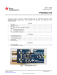
UM10469 48 V/150 W demo board using the SSL4101 Rev. 1.2 — 29 December 2014 User manual Document information Info Content Keywords SSL4101, GreenChip III+, SSL, low cost, LED driver, mains supply, user manual Abstract This document explains the basic operation and application of the 150 W SSL4101 Solid-State Lighting (SSL) driver evaluation board. The SSL4101 is designed to meet the needs of universal mains SSL drivers used in industrial and commercial lighting applications. UM10469 NXP Semiconductors 48 V/150 W demo board using the SSL4101 Revision history Rev Date Description v.1.2 20141229 third issue v.1.1 20120522 second issue v.1 20110517 first issue Contact information For more information, please visit: http://www.nxp.com For sales office addresses, please send an email to: [email protected] UM10469 User manual All information provided in this document is subject to legal disclaimers. Rev. 1.2 — 29 December 2014 © NXP Semiconductors N.V. 2014. All rights reserved. 2 of 17 UM10469 NXP Semiconductors 48 V/150 W demo board using the SSL4101 1. Introduction WARNING Lethal voltage and fire ignition hazard The non-insulated high voltages that are present when operating this product, constitute a risk of electric shock, personal injury, death and/or ignition of fire. This product is intended for evaluation purposes only. It shall be operated in a designated test area by personnel qualified according to local requirements and labor laws to work with non-insulated mains voltages and high-voltage circuits. This product shall never be operated unattended. This document explains the basic operation and application of the 150 W SSL4101 Solid-State Lighting (SSL) driver evaluation board. The device is designed to meet the requirements of universal mains SSL drivers used in industrial and commercial lighting applications. Both Constant Current Mode (CCM) or Constant Voltage Mode (CVM) outputs are supported over power ranges from 100 W to 280 W delivered to the load with minor modifications. The SSL4101 uses NXP Semiconductors GreenChip III+ Switched Mode Power Supply (SMPS) controller IC technology. The SSL4101 combines a controller for Power Factor Correction (PFC) and a flyback controller. The SSL4101’s high level of integration allows design of a cost-effective LED lighting applications in a small form factor using low number of components. Remark: In this user manual, all voltages are in V (AC) unless otherwise specified. 019aac388 Fig 1. UM10469 User manual SSL4101 demo board All information provided in this document is subject to legal disclaimers. Rev. 1.2 — 29 December 2014 © NXP Semiconductors N.V. 2014. All rights reserved. 3 of 17 UM10469 NXP Semiconductors 48 V/150 W demo board using the SSL4101 2. Safety warning The board can be connected to a mains voltage between 108 V and 305 V. A different mains voltage range can be selected with minor modifications. The output connected to the LEDs is designed for reinforced isolation from the mains. The demo board is designed to meet UL1950, UL8750 and EN61347 but was not submitted for safety compliance. Touching the reference board during operation must be avoided at all times. An isolated housing for the board and the LED's is mandatory when used in uncontrolled, non-laboratory environments. Therefore the board must be connected to the mains supply via a galvanic isolated (variable) transformer. These devices can be recognized by the symbols shown in Figure 2. 019aab174 019aab173 a. Isolated Fig 2. b. Not isolated Variac isolation symbols 3. SSL4101 driver board specifications Table 1. SSL4101 driver board specifications Symbol Parameter Name Minimum Units Remarks Toper operating temperature 25 to +60; 40 to +85; +5 to +95 +0 to +95 Target C/% ambient temperature; non-condensing relative humidity VI input voltage (mains AC) 108 to 305 85 to 305 V - fi input frequency 49 to 61 47 to 63 Hz - Vo output voltage - 48; 2 % V output voltage must always stay below 60 V to meet the Class II operating requirements Io(max) maximum output current 3.1 - A unit must keep constant voltage output from no-load through maximum output current efficiency 91*/94 ** - % * measured with VI set to 120 V ** measured with VI set to 277 V (full load) PF Power Factor 0.95*** 0.9**** - Measured with VI set to 120 V; 230 V and 277 V *** at full load **** for loads from 50 % to full load Pstb standby power < 500 < 300 mW power in mW at no-load td(start) start-up delay time < 300 < 200 ms startup delay time from power-up until Io is above 90 % of its rated output current measured at maximum load UM10469 User manual All information provided in this document is subject to legal disclaimers. Rev. 1.2 — 29 December 2014 © NXP Semiconductors N.V. 2014. All rights reserved. 4 of 17 UM10469 NXP Semiconductors 48 V/150 W demo board using the SSL4101 4. SSL4101 driver overview The SSL4101 is part of NXP Semiconductors GreenChip III+ (third generation) of green Switched Mode Power Supply (SMPS) controller ICs. The SSL4101T combines both a controller for Power Factor Correction (PFC) and a flyback controller. The integrated green functions provide high-efficiency at all power levels. This applies to quasi-resonant operation at high power levels, quasi-resonant operation with valley skipping, as well as to reduced frequency operation at lower power levels. At low power levels, the PFC switches off to maintain the SSL4101’s high-efficiency. During low power conditions, the flyback controller switches to frequency reduction mode and limits the peak current to 25 % of its maximum value. This ensures high-efficiency at low power and good standby power performance while minimizing audible noise from the transformer. The SSL4101T is a MultiChip Module (MCM) containing two chips. The proprietary high voltage BCD800 process which makes direct start-up possible from the rectified universal mains voltage in an effective and green way. The second low voltage SIlicon On Insulator (SIO) is used for accurate, high speed protection functions and control. The SSL4101T enables extremely efficient and reliable LED lighting application power supplies with power requirements from 10 W to 300 W to be designed easily using the minimum number of additional components. UM10469 User manual All information provided in this document is subject to legal disclaimers. Rev. 1.2 — 29 December 2014 © NXP Semiconductors N.V. 2014. All rights reserved. 5 of 17 UM10469 NXP Semiconductors 48 V/150 W demo board using the SSL4101 PFCDRIVER PFC DRIVER 1.12 V PFC GATE 3.5 V FBDRIVER 12 13 DRV FB DRIVER 80 μA DRV 5 LATCH FB GATE EXT PROT LOW VIN 1.25 V VINSENSE 7 PROT MAX PFCCOMP 6 R PFC PROT PROT ENABLE PFC R Q Q S LOW POWER PFC OSC 3.7 V 2.50 V PFC PROT VoSTART FB VoSHORT PFCSENSE 11 SMPS CONTROL EXT PROT OTP FBOVP LATCH RESET BLANK OPP STARTFB START STOP PFC 3 FBCTRL MIN OCP FB DRIVER S S LATCHED S PROTECTION R TIMEOUT TON MAX VoSHORT VUVLO PFC DRIVER ENABLE PFC BLANK 10 FBSENSE SOFT START S SAFE S S RESTART PROTECTION R PROT EXT PROT Vstartup Vth(UVLO) 60 μA START STOP PFC ENABLE FB VCC GOOD CHARGE CHARGE CONTROL OPP OVP OvpFB INTERNAL SUPPLY OTP ZCS OPP VALLEY DETECT VALLEY DETECT PFCGATE 60 μA START SOFT START FB TIMER 4 μs PFCAUX 8 TIME OUT PROT OCP 500 mV 30 μA Freq. Red. VCC GOOD VoSTART FB LOW POWER EXT PROT LOW VIN FB OSC TON MAX 2.7 V VoOVP 3.5 V LOW POWER 1.25 V VOSENSE 9 2.5 V Freq Red. ENABLE FB S COUNTER 4 FBAUX CHARGE Vstartup FB GATE ZCS TIMER 50 μs Vth(UVLO) OTP TEMP 80 mV 100 mV 16 2 1 HV VCC GND 001aan671 Remark: The time-out is the safe restart for the SSL4101T. Fig 3. Block diagram 5. Pin description 5.1 Pin configuration VCC 1 16 HV GND 2 15 HVS FBCTRL 3 14 HVS FBAUX 4 13 FBDRIVER SSL4101T LATCH 5 12 PFCDRIVER PFCCOMP 6 11 PFCSENSE VINSENSE 7 10 FBSENSE PFCAUX 8 9 VOSENSE 001aan672 Fig 4. UM10469 User manual Pin configuration diagram All information provided in this document is subject to legal disclaimers. Rev. 1.2 — 29 December 2014 © NXP Semiconductors N.V. 2014. All rights reserved. 6 of 17 UM10469 NXP Semiconductors 48 V/150 W demo board using the SSL4101 5.2 Pin description Table 2. Pin description Symbol Pin Description VCC 1 supply voltage GND 2 ground FBCTRL 3 control input for flyback FBAUX 4 input from auxiliary winding for demagnetization timing and overvoltage protection for flyback LATCH 5 general purpose protection input PFCCOMP 6 frequency compensation pin for PFC VINSENSE 7 sense input for mains voltage PFCAUX 8 input from auxiliary winding for demagnetization timing for PFC VOSENSE 9 sense input for PFC output voltage FBSENSE 10 programmable current sense input for flyback PFCSENSE 11 programmable current sense input for PFC PFCDRIVER 12 gate driver output for PFC FBDRIVER 13 gate driver output for flyback HVS 14; 15 high voltage safety spacer; not connected HV 16 high voltage start-up and valley sensing of flyback part 6. Schematic SSL4101 demo board The major components of a typical SSL4101 application are shown in Figure 5. The following remarks are very important when designing your application. Remark: Minimize both the perimeters and the areas encircled by the indicated loops. Remark: Power and signal GND must have only one connection between the C22 ground pin and the C7 minus pin. Remark: In Figure 5 the connections for some capacitors must be soldered directly to the capacitors solder point on the PCB and from that point connected to the next component. Remark: Components that are not parts of the power loops, particularly the ICs and the filter capacitors must not be enclosed by a power loop. Moreover, they should be kept as far from them as possible. UM10469 User manual All information provided in this document is subject to legal disclaimers. Rev. 1.2 — 29 December 2014 © NXP Semiconductors N.V. 2014. All rights reserved. 7 of 17 xxxxxxxxxxxxxxxxxxxxx xxxxxxxxxxxxxxxxxxxxxxxxxx xxxxxxx x x x xxxxxxxxxxxxxxxxxxxxxxxxxxxxxx xxxxxxxxxxxxxxxxxxx xx xx xxxxx xxxxxxxxxxxxxxxxxxxxxxxxxxx xxxxxxxxxxxxxxxxxxx xxxxxx xxxxxxxxxxxxxxxxxxxxxxxxxxxxxxxxxxx xxxxxxxxxxxx x x xxxxxxxxxxxxxxxxxxxxx xxxxxxxxxxxxxxxxxxxxxxxxxxxxxx xxxxx xxxxxxxxxxxxxxxxxxxxxxxxxxxxxxxxxxxxxxxxxxxxxxxxxx xxxxxxxx xxxxxxxxxxxxxxxxxxxxxxxxx xxxxxxxxxxxxxxxxxxxx xxx L2 5 mH L3 C3 4.7 nF Y2 C1 470 nF X2 3 C2 4.7 nF Y2 E1 1.5 Arms 2 R3 1 MΩ 1 % HV C4 100 nF X2 E3 primary D1 GBU806 +441 V (DC) 696 μH R2 1 MΩ 1 % HV L4 D2 L6 LPB-320u-4A3FX BYV25D-600 L5 R4 4.7 MΩ 1 % HV C6 470 nF X2 68 μH (1) C5 108-305 V (AC) E3 100 nF X2 E2 D6 (2) PMEG2005ET R10 J1 D12 1 D16 SMBJ78A C26 33 μF (35 V) BAS21J 2 D3 SMBJ78A +48 V (DC) TB2 15 A R8 20 kΩ (0.5 W) C8 4.7 nF Y2 R6 53.6 kΩ 1% C12 10 nF C10 1 nF (350 V) C9 10 nF (1 kV) R5 4.7 MΩ 1 % HV (1) (1) C7 68 μF (500 V) +19 V (DC) secondary T1 TPK-710u-2A6FX C28 390 μF (63 V) D4 C27 1 C29 390 μF (63 V) R31 SMAJ100A 150 pF 220 Ω (200 V) (2) Q1 IPA60R385CP (1) E3 E3 Q3 PSMN057-200P HES_3323_B R16 2Ω (0.25 W) R17 1 kΩ R11 R12 12 kΩ C13 0.091 Ω 1 % (1 W) D5 MUR1100E E4 D7 PMEG2005ET 100 nF R18 2Ω (0.25 W) 10 Ω (0.25 W) 10 11 1 kΩ 15 kΩ 1 kΩ R15 0.16 Ω 1 % (1 W) C15 13 14 15 (1) BAS21J C23 33 μF (35 V) R9 220 Ω U3 8 C17 3 D10 PMBD914 output power loop Aux. supply power loops R23 61.9 kΩ (2) C18 2.2 μF (10 V) (2) R25 33 kΩ C19 470 nF (16 V) (2) C21 10 nF (2) (2) R27 NTC 100 kΩ (2) (1) Primary power GND, all connections go to the C7 minus pin. (2) Primary signal GND, all connections go to the C22 ground pin. Fig 5. Schematic SSL4101 demo board R45 0Ω 4 6 5 +19 V (DC) C33 +48 V (DC) R44 1 nF 10 kΩ 19 V (DC) C22 100 nF (2) R46 100 kΩ D11 C32 100 nF 3 C34 PMBD914 R41 220 Ω R29 R30 287 kΩ 1% 66.5 kΩ 1% 4 R26 10 kΩ C20 150 nF (16 V) 3 1 R28 39 kΩ C35 R37 10 nF 10 kΩ R39 93.1 kΩ 1% U2 HCPL-817-W6CE R38 47 nF 10 kΩ R43 R36 287 kΩ 1% C36 22 nF 1 MΩ R40 4.99 kΩ 1% (3) (3) C24 10 nF (2) C25 330 nF (16 V) (2) 3 2 (2) 019aac283 UM10469 8 of 17 © NXP Semiconductors N.V. 2014. All rights reserved. flyback power loop +19 V (DC) 1 (2) (2) PFC unductor discharge loop 2 VCC FBAUX LATCH 4 GND 5 FBCTRL 6 PFCCMP VINSNS PFCAUX R24 1 MΩ 1% PFC unductor charge loop 7 7 VCC (2) 8 2 R47 2Ω (0.25 W) TEA1761 SSL4101 1 nF (100 V) (3) 1 C11 220 pF (100 V) U1 16 E5 Q4 PBSS4032NT D15 PMEG2005ET D8 HV n.c. 220 nF n.c. FBDRV 12 R35 4.99 kΩ 1% R20 ISENSE 9 R14 (2) PFCDRV PFCSNS FBSNS VOSNS C16 470 pF R19 GND R22 1 MΩ 1% R34 2Ω (0.25 W) R33 1 kΩ R13 SRSENSE (2) C31 68 nF X2 (3) (1) Q2 SPA08N80C3 C14 470 pF 0.015 Ω 2010 48 V/150 W demo board using the SSL4101 Rev. 1.2 — 29 December 2014 All information provided in this document is subject to legal disclaimers. R21 5.1 kΩ 2 R32 (1) 10 Ω (0.25 W) H1 C30 100 nF DRIVER 4A n.c. NTC 7R-2A 68 μH OPTO L1 4 mH F1 1 VSENSE R1 NXP Semiconductors UM10469 User manual TB1 8 A (300 V) UM10469 NXP Semiconductors 48 V/150 W demo board using the SSL4101 7. Bill of materials Table 3. Bill of materials Component Qty Description Manufacturer and type C1; C6 2 film capacitor; 470 nF; 305 V (AC); X2 EPCOS; B32922C3474M C2; C3; C8 3 ceramic capacitor; 4.7 nF; 300 V (AC); Y2; disc Vishay; VY2472M49Y5US63V7 C4 1 film capacitor; 100 nF; 305 V (AC); X2; 10 mm LdSp EPCOS; B32921C3104M C5 1 film capacitor; 100 nF; 305 V (AC); X2; 15 mm LdSp EPCOS; B32922A2104M C7 1 electrolytic capacitor; 68 F; 500 V; 0.78 A to 1.1 A Panasonic; ECO-S2HP680CA (RMS) C9 1 ceramic capacitor; 10 nF; 1 kV; 20 to +80 %; disc Murata; DEBE33A103ZA3B C10 1 ceramic capacitor; 1 nF; 300 V (AC); Y2; disc Vishay; VY2102M29Y5US63V7 C11 1 MLCC; 220 pF; 100 V; 10 %; X7R; SMD 0805 AVX; 08051C221KAT2A C12; C21; C24 3 MLCC; 10 nF; 50 V; 10 %; X7R; SMD 0805 AVX; 08055C103KAT2A C13; C22 2 MLCC; 100 nF; 100 V; 10 %; X7R; SMD 0805 TDK; C2012X7R2A104K C14; C16 2 MLCC; 470 pF; 100 V; 5 %; NPO; SMD 0805 TDK; C2012COG2A471J C15 1 MLCC; 220 nF; 16 V; 10 %; X7R; SMD 0805 Murata; GRM219R71C224KA01D C17; C33 2 MLCC; 1 nF; 100 V; 10 %; X7R; SMD 0805 AVX; 08051C102KAT2A C18 1 MLCC; 2.2 ?F; 10 V; 10 %; X7R; SMD 0805 Murata; GRM21BR71A225KA01L C19 1 MLCC; 470 nF; 16 V; 10 %; X7R; SMD 0805 Panasonic; ECJ-2FB1C474K C20 1 MLCC; 150 nF; 16 V; 10 %; X7R; SMD 0805 AVX; 0805YC153KAT2A C23; C26 2 electrolytic capacitor; 33 F; 35 V; 105 C; 0.175 A Nippon Chemi-Con; ELXZ350ELL330MEB5D (RMS) C25 1 MLCC; 330 nF; 16 V; 10 %; X7R; SMD 0805 AVX; 0805YC334KAT2A C27 1 MLCC; 150 pF; 200 V; 10 %; NPO; SMD 1206 - C31 1 film capacitor; 68 nF; 305 V (AC); X2 Vishay; BFC233820683 C28; C29 2 electrolytic capacitor; 390 F; 63 V; 1.9 A (RMS) Nippon Chemi-Con; EKZE630ELL391MK25S C30; C32 2 MLCC; 100 nF; 100 V; 10 %; X7R; SMD 0805 TDK; C2012X7R2A104K C35 1 MLCC; 47 nF; 50 V; 10 %; X7R; SMD 0805 AVX; 08055C473KAT2A C34 1 MLCC; 10 nF; 50 V; 10 %; X7R; SMD 0805 AVX; 08055C103KAT2A C36 1 MLCC; 22 nF; 50 V; 10 %; X7R; SMD 0805 AVX; 08055C223KAT2A D1 1 diode bridge; 8 A; 600 V; GBU806 Diodes Incorporated; GBU806 D2 1 diode; 5 A; 600 V; ultrafast; DPAK NXP Semiconductors; BYV25D-600 D3; D16 2 diode; Zener; 91 V; 5 %; 5 W; SMB Littelfuse; SMBJ78A D4 1 diode; Zener; 117 V; 5 %; 3 W; SMA Littelfuse; SMAJ100A D5 1 diode; 1 A; 1 kV; ultrafast; DO-41 ON Semiconductor; MUR1100E D6; D7 2 diode; Schottky; 0.5 A; 20 V; SOT23 NXP Semiconductors; PMEG2005ET D8; D12 2 diode; 0.25 A; 300 V; fast recovery; SOD323F NXP Semiconductors; BAS21J D10; D11 2 diode; 0.2 A; 100 V; high speed switching; SOT23 NXP Semiconductors; PMBD914 D15 1 diode; Schottky; 0.5 A; 20 V; SOT23 NXP Semiconductor; PMEG2005ET F1 1 fuse; 4 A; 300 V; time-lag Littelfuse; 3691400044 UM10469 User manual All information provided in this document is subject to legal disclaimers. Rev. 1.2 — 29 December 2014 © NXP Semiconductors N.V. 2014. All rights reserved. 9 of 17 UM10469 NXP Semiconductors 48 V/150 W demo board using the SSL4101 Table 3. Bill of materials …continued Component Qty Description Manufacturer and type H1 1 heat sink spreader; D1; Q1; Q2; D13/Q3 Custom; HCC-8706-BlkA1 case 1 case; 12.45 mm 6.35 mm 3.89 mm (4.90" 2.50" 1.53"); yellow anodized Custom; HCC-4925-YelA1 case top 1 case top; 12.45 mm 6.05 mm 0.51 mm (4.90" 2.38" 0.20"); yellow anodized Custom; HCC-4924-YelA1 J1 1 connector; RCPT; 2 POS; .100";SNGL GOLD Samtec Inc; CES-102-01-S-S L1 1 inductor; common mode; 4 mH; 2 A; 10 k; split Würth Elektronik 750312184 L2 1 inductor; common mode; 5 mH; 2 A; 10 k; bifilar Würth Elektronik 750312185 L3; L4 2 inductor; differential mode; 68 H; 2 A Murata; 13R683C L5 1 inductor; differential mode; 696 H; 2 A; high flux 160 u Würth Elektronik 750341186 L6 1 inductor; 320 H; RM10-3C95; 47.5T; 40/38 SPNSN Served Litz Würth Elecktronik 750312188 R1 1 NTC resistor; 7 ; 2 A Ametherm; SL08 7R002 R2; R3 2 resistor; 1 M; 1 %; SMD 1206; high voltage Rohm; KTR18EZPF1004 R4; R5 2 resistor; 4.7 M; 1 %; SMD 1206; high voltage Rohm; KTR18EZPF4704 R6 1 resistor; 53.6 k; 0.125 W; 1 %; SMD 0805 Yageo; RC0805FR-0753K6L R8 1 resistor; 20 k; 0.5 W; 1 %; SMD 1206 Stackpole Electronics; RNCP1206FTD20K0 R9 1 resistor; 220 ; 0.125 W; 5 %; SMD 0805 Stackpole Electronics; RMCF0805JT220R R10; R13 2 resistor; 10 ; 0.25 W; 5 %; SMD 1206 Stackpole Electronics; RMCF1206JT10R0 R11 1 resistor; 12 k; 0.125 W; 5 %; SMD 0805 Stackpole Electronics; RMCF 1/10 12K 5% R R14 1 resistor; 15 k; 0.125 W; 5 %; SMD 0805 Stackpole Electronics; RMCF 1/10 15K 5% R R12 1 resistor; 0.091 ; 1 W; 1 %; SMD 2010 Stackpole Electronics; CSRN2010FKR091 R15 1 resistor; 0.16 ; 1 W; 1 %; SMD 2010 Stackpole Electronics; CSRN2010FKR160 R16; R18 2 resistor; 2 ; 0.25 W; 5 %; SMD 1206 Panasonic; ERJ-8GEYJ2R0V R17; R19; R20 3 resistor; 1 k; 0.125 W; 5 %; SMD 0805 Stackpole Electronics; RMCF 1/10 1K 5% R R21 1 resistor; 5.1 k; 0.125 W; 5 %; SMD 0805 Stackpole Electronics; RMCF 1/10 5.1K 5% R R22; R24 2 resistor; 1 M; 1 %; SMD 0805 Stackpole Electronics; RMCF0805FT1M00 R23 1 resistor; 61.9 k; 0.125 W; 1 %; SMD 0805 Yageo; RC0805FR-0761K9L R25 1 resistor; 33 k; 0.125 W; 5 %; SMD 0805 Stackpole Electronics; RMCF 1/10 33K 5% R R26 1 resistor; 10 k; 0.125 W; 1 %; SMD 0805 Stackpole Electronics; RMCF 1/10 10K 1% R R27 1 NTC Resistor; 100 k; 5 %; 3950-4400 B25/50 Cantherm; MF52A104J3950 R28 1 resistor; 39 k; 0.125 W; 5 %; SMD 0805 Stackpole Electronics; RMCF 1/10 39K 5% R R29; R36 2 resistor; 287 k; 0.125 W; 1 %; SMD 0805 Stackpole Electronics; RMCF0805FT287K R30 1 resistor; 66.5 k; 0.125 W; 1 %; SMD 0805 Yageo; RC0805FR-0766K5L R31; R41 2 resistor; 220 ; 0.125 W; 5 %; SMD 0805 Stackpole Electronics; RMCF 1/10 220 5% R R33 1 resistor; 1 k; 0.125 W; 5 %; SMD 0805 Stackpole Electronics; RMCF 1/10 1K 5% R R32 1 resistor; 0.015 ; 1 W; 1 %; SMD 2010 Stackpole Electronics; CSRN2010FKR015 R34; R47 2 resistor; 2 ; 0.25 W; 5 %; SMD 1206 Panasonic; ERJ-8GEYJ2R0V R35; R40 2 resistor; 4.99 k; 0.125 W; 1 %; SMD 0805 Stackpole Electronics; RMCF 1/10 4.99K 1% R R37; R38; R44 3 resistor; 10 k; 0.125 W; 1 %; SMD 0805 Stackpole Electronics; RMCF 1/10 10K 1% R R39 1 resistor; 93.1 k; 0.125 W; 1 %; SMD 0805 Stackpole Electronics; RMCF0805FG93K1 UM10469 User manual All information provided in this document is subject to legal disclaimers. Rev. 1.2 — 29 December 2014 © NXP Semiconductors N.V. 2014. All rights reserved. 10 of 17 UM10469 NXP Semiconductors 48 V/150 W demo board using the SSL4101 Table 3. Bill of materials …continued Component Qty Description Manufacturer and type R43 1 resistor; 1 M; 1 %; SMD 0805 Stackpole Electronics; RMCF0805FT1M00 R45 1 resistor; 0 ; SMD 0805 Stackpole Electronics; Jumper R46 1 resistor; 100 k; 0.125 W; 1 %; SMD 0805 Stackpole Electronics; RMCF0805FT100K SMPS designed; ADx-yyyW-PCBC1 PCB1 1 PCB; double-sided Q1 1 MOSFET; 650 V; 5.7 A; 0.63 at 100 C; TO220F Infineon; IPA60R385CP Q2 1 MOSFET; 800 V; 5.1 A; 1.08 at 100 C; TO220F Infineon; SPA08N80C3 Q3 1 MOSFET; 200 V; 27 A; 73 m at 100 C; TO220 NXP Semiconductor; PSMN057-200P Q4 1 NPN; 30 V; 2 A; SOT23 NXP Semiconductor; PBSS4032NT T1 1 transformer; flyback; PQ32/20-3C95; 710 H; 40 : 10: 4 : 4 Würth Elecktronik 750341026 TB1 1 terminal block; 3 15 A; 300 V (AC) On-Shore Technology; OSTTC032162 TB2 1 terminal block; 2 16 A; 250 V (AC) On-Shore Technology; OSTTC020162 U1 1 IC; GreenChip III SMPS Controller NXP Semiconductors; SSL4101 U2 1 optocoupler; CTR = 200-400 Avago Technologies; HCPL-817-W6CE U3 1 IC; GreenChip synchronous rectifier controller NXP Semiconductor; TEA1761T (C7) 1 nomex insulator; 0.254 mm (10 mil); 2.67 mm (1.050") - (case top) 6 screw; #2-56; 3.17 mm (1/8") length; flat head; undercut; stainless steel McMaster; 91771A074 1 copper shield; 0.127 mm (5 mil); 5.51 mm 1.78 mm (2.170" 0.700") - (case) 2 nomex strip; 1.63 mm 12.31 mm (0.640" 4.850") - (D1; Q1; Q2; D13/Q3) 4 screw; #4-40; 7.94 mm (5/16") length; flat head; undercut; stainless steel McMaster; 91099A160 (D1; Q1; Q2; D13/Q3) 4 belleville washer; #4 McMaster; 9713K54 (D1; Q1; Q2; D13/Q3) 4 hex nut; #4; stainless steel McMaster; 91841A005 (E1-E5) 5 screw; #4-40; 6.35 mm (1/4"); pan head; external washer; zinc plated steel McMaster; 90402A106 (H1) 6 screw; #4-40; 1/8" length; flat head; undercut; stainless steel McMaster; 91771A103 (L5) 1 nomex insulator; 0.254 mm (10 mil); 1.27 mm 2.54 mm (0.500" 1.000") - (L6) 1 nomex insulator; 0.254 mm (10 mil); 2.54 mm 2.54 mm (1.000" 1.000") - (R27) 2 heatshrink tubing; 0.127 mm (0.050"); long 0.76 mm (0.300") - (T1) 1 nomex insulator; 0.254 mm (10 mil); 3.43 mm 3.56 mm (1.350" 1.400") - UM10469 User manual All information provided in this document is subject to legal disclaimers. Rev. 1.2 — 29 December 2014 © NXP Semiconductors N.V. 2014. All rights reserved. 11 of 17 UM10469 NXP Semiconductors 48 V/150 W demo board using the SSL4101 8. Operation and connection line SSL4101 AC VIN neutral ACTIVE PFC AND FLYBACK SSL DRIVER TB2-1 +output TB2-2 -output J1-1 +AUX out J1-2 -AUX out 019aac389 earth GND Fig 6. General connection of the SSL4101 demo board 019aac390 Fig 7. Input side UM10469 User manual 019aac391 Fig 8. Output side All information provided in this document is subject to legal disclaimers. Rev. 1.2 — 29 December 2014 © NXP Semiconductors N.V. 2014. All rights reserved. 12 of 17 UM10469 NXP Semiconductors 48 V/150 W demo board using the SSL4101 9. Measurements 019aac392 97 η (%) (1) 95 (2) 93 (3) 91 89 0 50 100 150 DC load (W) (1) 277 V (AC). (2) 230 V (AC). (3) 120 V (AC). Fig 9. Efficiency () as a function of as a function of DC output power (Po) 019aac393 1.00 (3) PF 0.95 (2) 0.90 (1) 0.85 0.80 0 50 100 150 DC load (W) (1) 277 V (AC). (2) 230 V (AC). (3) 120 V (AC). Fig 10. Power factor as a function of as a function of DC output power (Po) UM10469 User manual All information provided in this document is subject to legal disclaimers. Rev. 1.2 — 29 December 2014 © NXP Semiconductors N.V. 2014. All rights reserved. 13 of 17 UM10469 NXP Semiconductors 48 V/150 W demo board using the SSL4101 019aac394 19 II THD (%) 14 (1) (2) 9 (3) 4 0 50 100 150 DC load (W) (1) 277 V (AC). (2) 230 V (AC). (3) 120 V (AC). Fig 11. Input current (II) THD as a function of DC output power (Po) 019aac395 500 Pstby (mW) 400 (1) 300 200 100 100 (2) 150 200 250 300 RMS input voltage (V) (1) 80 mW. (2) No-load. Fig 12. Standby power (Pstby) as a function of as a function of input voltage (VI (RMS)) UM10469 User manual All information provided in this document is subject to legal disclaimers. Rev. 1.2 — 29 December 2014 © NXP Semiconductors N.V. 2014. All rights reserved. 14 of 17 UM10469 NXP Semiconductors 48 V/150 W demo board using the SSL4101 10. PCB layouts 019aac396 a. Top view 019aac397 b. Bottom view Fig 13. SSL4101 Gerber files 11. References UM10469 User manual [1] AN11054 — GreenChip III+ SSL4101 integrated PFC and flyback controller application note. [2] SSL4101T — Data sheet. All information provided in this document is subject to legal disclaimers. Rev. 1.2 — 29 December 2014 © NXP Semiconductors N.V. 2014. All rights reserved. 15 of 17 UM10469 NXP Semiconductors 48 V/150 W demo board using the SSL4101 12. Legal information 12.1 Definitions Draft — The document is a draft version only. The content is still under internal review and subject to formal approval, which may result in modifications or additions. NXP Semiconductors does not give any representations or warranties as to the accuracy or completeness of information included herein and shall have no liability for the consequences of use of such information. NXP Semiconductors does not accept any liability related to any default, damage, costs or problem which is based on any weakness or default in the customer’s applications or products, or the application or use by customer’s third party customer(s). Customer is responsible for doing all necessary testing for the customer’s applications and products using NXP Semiconductors products in order to avoid a default of the applications and the products or of the application or use by customer’s third party customer(s). NXP does not accept any liability in this respect. Export control — This document as well as the item(s) described herein may be subject to export control regulations. Export might require a prior authorization from competent authorities. 12.2 Disclaimers Limited warranty and liability — Information in this document is believed to be accurate and reliable. However, NXP Semiconductors does not give any representations or warranties, expressed or implied, as to the accuracy or completeness of such information and shall have no liability for the consequences of use of such information. NXP Semiconductors takes no responsibility for the content in this document if provided by an information source outside of NXP Semiconductors. In no event shall NXP Semiconductors be liable for any indirect, incidental, punitive, special or consequential damages (including - without limitation - lost profits, lost savings, business interruption, costs related to the removal or replacement of any products or rework charges) whether or not such damages are based on tort (including negligence), warranty, breach of contract or any other legal theory. Notwithstanding any damages that customer might incur for any reason whatsoever, NXP Semiconductors’ aggregate and cumulative liability towards customer for the products described herein shall be limited in accordance with the Terms and conditions of commercial sale of NXP Semiconductors. Right to make changes — NXP Semiconductors reserves the right to make changes to information published in this document, including without limitation specifications and product descriptions, at any time and without notice. This document supersedes and replaces all information supplied prior to the publication hereof. Suitability for use — NXP Semiconductors products are not designed, authorized or warranted to be suitable for use in life support, life-critical or safety-critical systems or equipment, nor in applications where failure or malfunction of an NXP Semiconductors product can reasonably be expected to result in personal injury, death or severe property or environmental damage. NXP Semiconductors and its suppliers accept no liability for inclusion and/or use of NXP Semiconductors products in such equipment or applications and therefore such inclusion and/or use is at the customer’s own risk. Applications — Applications that are described herein for any of these products are for illustrative purposes only. NXP Semiconductors makes no representation or warranty that such applications will be suitable for the specified use without further testing or modification. Customers are responsible for the design and operation of their applications and products using NXP Semiconductors products, and NXP Semiconductors accepts no liability for any assistance with applications or customer product design. It is customer’s sole responsibility to determine whether the NXP Semiconductors product is suitable and fit for the customer’s applications and products planned, as well as for the planned application and use of customer’s third party customer(s). Customers should provide appropriate design and operating safeguards to minimize the risks associated with their applications and products. Evaluation products — This product is provided on an “as is” and “with all faults” basis for evaluation purposes only. NXP Semiconductors, its affiliates and their suppliers expressly disclaim all warranties, whether express, implied or statutory, including but not limited to the implied warranties of non-infringement, merchantability and fitness for a particular purpose. The entire risk as to the quality, or arising out of the use or performance, of this product remains with customer. In no event shall NXP Semiconductors, its affiliates or their suppliers be liable to customer for any special, indirect, consequential, punitive or incidental damages (including without limitation damages for loss of business, business interruption, loss of use, loss of data or information, and the like) arising out the use of or inability to use the product, whether or not based on tort (including negligence), strict liability, breach of contract, breach of warranty or any other theory, even if advised of the possibility of such damages. Notwithstanding any damages that customer might incur for any reason whatsoever (including without limitation, all damages referenced above and all direct or general damages), the entire liability of NXP Semiconductors, its affiliates and their suppliers and customer’s exclusive remedy for all of the foregoing shall be limited to actual damages incurred by customer based on reasonable reliance up to the greater of the amount actually paid by customer for the product or five dollars (US$5.00). The foregoing limitations, exclusions and disclaimers shall apply to the maximum extent permitted by applicable law, even if any remedy fails of its essential purpose. Safety of high-voltage evaluation products — The non-insulated high voltages that are present when operating this product, constitute a risk of electric shock, personal injury, death and/or ignition of fire. This product is intended for evaluation purposes only. It shall be operated in a designated test area by personnel that is qualified according to local requirements and labor laws to work with non-insulated mains voltages and high-voltage circuits. The product does not comply with IEC 60950 based national or regional safety standards. NXP Semiconductors does not accept any liability for damages incurred due to inappropriate use of this product or related to non-insulated high voltages. Any use of this product is at customer’s own risk and liability. The customer shall fully indemnify and hold harmless NXP Semiconductors from any liability, damages and claims resulting from the use of the product. Translations — A non-English (translated) version of a document is for reference only. The English version shall prevail in case of any discrepancy between the translated and English versions. 12.3 Trademarks Notice: All referenced brands, product names, service names and trademarks are the property of their respective owners. GreenChip — is a trademark of NXP Semiconductors N.V. UM10469 User manual All information provided in this document is subject to legal disclaimers. Rev. 1.2 — 29 December 2014 © NXP Semiconductors N.V. 2014. All rights reserved. 16 of 17 UM10469 NXP Semiconductors 48 V/150 W demo board using the SSL4101 13. Contents 1 2 3 4 5 5.1 5.2 6 7 8 9 10 11 12 12.1 12.2 12.3 13 Introduction . . . . . . . . . . . . . . . . . . . . . . . . . . . . 3 Safety warning . . . . . . . . . . . . . . . . . . . . . . . . . . 4 SSL4101 driver board specifications . . . . . . . . 4 SSL4101 driver overview . . . . . . . . . . . . . . . . . 5 Pin description . . . . . . . . . . . . . . . . . . . . . . . . . . 6 Pin configuration . . . . . . . . . . . . . . . . . . . . . . . . 6 Pin description . . . . . . . . . . . . . . . . . . . . . . . . . 7 Schematic SSL4101 demo board . . . . . . . . . . . 7 Bill of materials . . . . . . . . . . . . . . . . . . . . . . . . . 9 Operation and connection . . . . . . . . . . . . . . . 12 Measurements . . . . . . . . . . . . . . . . . . . . . . . . . 13 PCB layouts . . . . . . . . . . . . . . . . . . . . . . . . . . . 15 References . . . . . . . . . . . . . . . . . . . . . . . . . . . . 15 Legal information. . . . . . . . . . . . . . . . . . . . . . . 16 Definitions . . . . . . . . . . . . . . . . . . . . . . . . . . . . 16 Disclaimers . . . . . . . . . . . . . . . . . . . . . . . . . . . 16 Trademarks. . . . . . . . . . . . . . . . . . . . . . . . . . . 16 Contents . . . . . . . . . . . . . . . . . . . . . . . . . . . . . . 17 Please be aware that important notices concerning this document and the product(s) described herein, have been included in section ‘Legal information’. © NXP Semiconductors N.V. 2014. All rights reserved. For more information, please visit: http://www.nxp.com For sales office addresses, please send an email to: [email protected] Date of release: 29 December 2014 Document identifier: UM10469