1
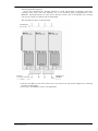
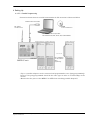
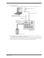
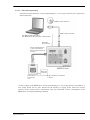
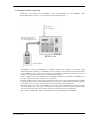
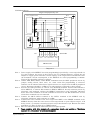
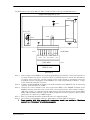
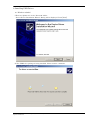
Multifunctional
Flash Microcomputer
Programmer
S550-MFW1U
Operation Manual
Sunny Giken Inc.
Multifunctional Flash Microcomputer Programmer
S550-MFW1U
The contents of this manual may be revised without notice.
We, Sunny Giken Inc. shall not be responsible for any damages and/or losses
caused by using this product and/or the software attached to this product claimed
by users and/or any intermediaries.
Specifications of this product and/or the software attached to this product may
be modified without notice for improvement.
The names of systems, products, and/or services used in this manual are either
registered trademarks or trademarks of each manufacturer.
The captions of the TM and (R) are not mentioned in this manual.
Multifunctional Flash Microcomputer [S550-MFW1U]
Operation Manual
1
1 Outline ........................................................................................................................................................3
1.1 Precautions ..........................................................................................................................................3
1.2 System Configuration..........................................................................................................................4
2 Specifications ..............................................................................................................................................5
2.1 General Specifications.........................................................................................................................5
2.2 Function Specifications .......................................................................................................................6
2.3 Programmable Devices........................................................................................................................7
3 Panel Description .......................................................................................................................................8
3.1 MFW1U Unit .......................................................................................................................................8
3.2 Parallel Adapter.................................................................................................................................10
4 Setting Up.................................................................................................................................................12
4.1 PC + Parallel Programming..............................................................................................................12
4.2 PC + Serial Programming .................................................................................................................13
4.3 PC + Onboard Programming ............................................................................................................14
4.4 Standalone Parallel Programming ...................................................................................................15
4.5 Standalone Serial Programming ......................................................................................................16
4.6 Standalone Onboard Programming..................................................................................................17
5 Connector Pin Specifications for Serial Programming ..........................................................................18
5.1 Connector (MFW1U Unit).................................................................................................................18
5.2 Pin Assignment (MFW1U Unit) .......................................................................................................18
5.3 Serial Programming Cable................................................................................................................19
5.4 Connection Circuit Example for the MFW1U .................................................................................20
6 Updating Firmware..................................................................................................................................38
7 MFW1U Standalone Operation...............................................................................................................39
7.1 Standalone Programming to Parallel Adapter ................................................................................39
7.2 Standalone Programming to Serial Adapter....................................................................................40
7.3 Standalone Programming to User Target Board.............................................................................40
7.4 Initializing Memory...........................................................................................................................41
7.5 List of LED Status.............................................................................................................................42
7.6 List of Beep Sounds ...........................................................................................................................42
8 Contact Check...........................................................................................................................................43
9 Installing USB Driver ..............................................................................................................................44
9.1 Windows 7(32bit) ...............................................................................................................................44
9.2 Windows 7(64bit) ...............................................................................................................................46
9.3 Others (Windows XP, 2000, Me, 98) .................................................................................................48
Multifunctional Flash Microcomputer [S550-MFW1U]
Operation Manual
2
1 Outline
1.1 Precautions
Thank you for purchasing our product S550-MFW1U, the Multifunctional Flash
Microcomputer Programmer.
Please read this operation manual carefully to understand the function of this product for
effective and stable operation. Please beware that Sunny Giken Inc. shall have no liability
for any damage and/or troubles caused by misuse or careless handling.
1) General Caution
Please follow the precautions mentioned below to avoid hazards such as fire, burns, electric
shock, and/or injures.
• Make sure that the power switch of this product is turned OFF and your hands are clean
and dry when an AC adapter is plugged in.
• Use this product under proper environment.
• Never place this product up-side-down or lateral side facing to table.
• Handle this product with care to avoid fall and/or physical shock.
• Never take this product apart and/or modify by yourself.
2) Use Environment
• Unusable environment
Dusty place
Place in the presence of corrosive gasses
Place exposed to direct sunlight
Place surrounded by equipment which originates noises
Place with severe mechanical shock and/or constant mechanical vibration
• Ambient temperature
0°C to +40°C
Humidity: below 80% (non condensing)
• Prevention of electrostatic buildup for operation of this product and devices is
recommended.
3) Storage
• Place this product into the packing box which had been delivered when your purchase and
store at shaded place with the ambient temperature of -10°C to +40°C and below 80% of
humidity (non condensing) for long term storage.
4) Transportation
• In case the product is needed to be relocated, use the packing box which had been delivered
when your purchase.
5) Cleaning
• Wipe the product with soft and clean fabric. Never use any sort of organic solvent such as
benzine that may cause this product deteriorated.
Multifunctional Flash Microcomputer [S550-MFW1U]
Operation Manual
3
1.2 System Configuration
The entire system configuration of the Multifunctional Flash Microcomputer Programmer
(hereinafter called “MFW1U”) is illustrated below.
MFW Control Software
USB Connecting Cable
PC: IBM PC/AT Compatible
OS: Windows98, Me, 2000, XP,
Windows7(32bit/64bit)
DC Cable
(for Oversea)
Parallel adapter
Cable for serial programming
(hereinafter called the "serialcable")
Target board or connector at the serial
adapter side should be prepare by
user.)
MFW1U unit
Serial adapter
Target board
Prepared by user
Up to 8 adapters can be
attached. Gang prgramming)
* The AC adapter is not attached for the export-product.
* Refer to the “4. Setting Up” for detailed and varied connection.
Multifunctional Flash Microcomputer [S550-MFW1U]
Operation Manual
4
2 Specifications
2.1 General Specifications
Unit of the MFW1U
MFW1U
DC + 9V lower than 1A AC adapter attached (for domestic use only)
Power capacity
(Use an attached DC cable for oversea use.)
Ambient temperature: 0°C to 40°C
Use environment
Humidity:
below 80% (non condensing)
Storage
Ambient temperature: -10°C to +40°C
environment
Power draw
AC 100V lower than 15VA 50/60 Hz (AC adapter)
Outer dimensions
125 (W) x 100 (D) x 25 (H) mm (Projection not included)
Weight
Less than 400g (only unit)
CE mark obtained (EMI: EN55011 Group1 Class A, EMS: EN61000-6-2)
Oversea
standards
FCC compliance
This device complies with part 15 of the FCC Rules. Operation is subject to the following two
conditions;
(1) This device may not cause harmful interference, and (2) this device must accept any
interference received, including interference that may cause undesired operation.
Parallel Adapter
Outer
162 (W) x 53 (D) x 16 (H) mm (Projection not included)
dimensions
Weight
Less than 400g
* Beware that the shape of the IC socket of the parallel adapter is varied from to be attached
device type. The height (16mm) mentioned at the above “Outer dimensions” is only size of
the case.
The polarity of this DC cable is illustrated below.
500mm
Wire color
Multifunctional Flash Microcomputer [S550-MFW1U]
Operation Manual
RED:DC+9V
BLACK:GND
5
2.2 Function Specifications
Programmable
MCU
Operation Mode
Renesas Electronics On-chip Flash Memory Microcomputer
Parallel I/O mode (gang programmable: up to 8 devices can be programmed
at once.) <Auto device set number detection and contact check function
are available>
Standard serial I/O mode (clock synchronous serial I/O and single wire
clock asynchronous serial I/O(applicable to R8C Family ))
* Clock asynchronous serial I/O mode not supported.
PC + parallel programming
PC + serial programming
Program Mode
PC + onboard programming
Standalone parallel programming
Standalone serial programming
Standalone onboard programming
Program data
Size
PC control
Software
Interface
Max: 1Mbyte
All the operation can be achieved from your PC with easy-to-operate GUI
(graphic user interface).
Applicable to the Win98, Me, 2000, XP,
7(32bit/64bit)
USB 1.1 supported (Full-speed Mode)
Multifunctional Flash Microcomputer [S550-MFW1U]
Operation Manual
6
2.3 Programmable Devices
The devices from the Renesas Electronics On-chip Flash Memory Microcomputer M16C
Family are programmable by the MFW1U. Some of devices are still under evaluation or
not programmable. Refer to the file “Programmable Device List” in an attachment floppy
disk.Contact Sunny Giken Inc. for the latest information.
Multifunctional Flash Microcomputer [S550-MFW1U]
Operation Manual
7
3 Panel Description
3.1 MFW1U Unit
External views of the MFW1U are shown and its parts such as switches, LEDs, and
connectors are also described.
• Top view
S550-MFW1U
M ult i Flash W riter
SERIAL
SOCKET
TARGET
PARALLEL
SOCKET
POWER
START
PASS
ID ERR
Switch/LED
POWER
Switch
LED
Buzzer
FAIL
Function
Power Off/ON switch (Power lamp available)
PARALLEL
SOCKET
SERIAL
SOCKET
SERIAL
TARGET
PASS
Starts programming. Data that had been loaded can be cleared by
pressing the “START” switch more than 5 seconds.
Turns it ON when programming target is parallel adapter with
definition by PC.
Turns it ON when programming target is serial adapter with
definition by PC.
Turns it ON when programming target is user target board with
definition by PC.
Turns it ON when serial programming is successful.
ID ERR
Turns it ON when result of serial programming is ID_ERR.
FAIL
Turns it ON when serial programming is failed.
START
Sounds when operation is completed or error is issued.
Multifunctional Flash Microcomputer [S550-MFW1U]
Operation Manual
8
• Back view
USB
DC9VIN
Connector
Function
DC9VIN
DC + 9V power jack
φ5.15 holes, Center φ1.65mm (compliance:EIAJ RC-5320 class3)
USB
USB communication connector (connected to PC)
• Left-hand side view
SERIAL
Connector
SERIAL
Function
Serial programming connector for target board or serial adapter.
• Right-hand side view
PARALLEL
Connector
PARALLEL
Function
Parallel programming connector for parallel adapter.
Multifunctional Flash Microcomputer [S550-MFW1U]
Operation Manual
9
3.2 Parallel Adapter
At the next, external views of the parallel adapter are shown and its parts such as LEDs and
connectors are also described.
LED/Connector
Function
Socket
Mounter socket for device programming.
PASS LED
Turns it ON when parallel programming is successful.
FAIL LED
Turns it ON when parallel programming is failed.
Connector 1
Parallel programming connector from the MFW1U.
Gang parallel programming connector when more than one parallel
Connector 2
adapters attached.
* The shape of the IC socket of the parallel adapter is varied from to be attached device type.
Refer to separate “Programmable Device List” for your order.
* Up to 8 parallel adapters can be connected and programmed at once (gang programming). But to be
gang programmed devices should be the same type to avoid breakage of devices.
Multifunctional Flash Microcomputer [S550-MFW1U]
Operation Manual
10
Attaching parallel adapters
Secure the attachment by placing latch(es) to avoid fail-to-make of adapters and safer
carriage when more than one adapters are to be attached (gang programming) to the
MFW1U. Latch-placement for only device mounter socket side is acceptable but securing
also at the topside is reliable and recommended.
The attachment figure is shown below
Latch(es) at
the top side
Latch(es)
at mounter socket side
M2.6 Screw
* Unscrew the M2.6 screws that hold a case cover and screw and attach adapters by referring
the above illustration.
* Screwing to the MFW1U unit is not applicable.
Multifunctional Flash Microcomputer [S550-MFW1U]
Operation Manual
11
4 Setting Up
4.1 PC + Parallel Programming
Connection instructions for parallel programming by PC operation is illustrated below.
USB Connection Cable
DC Cable
(for Oversea)
MFW
Control Software
PC: IBM PC/AT Compatible
OS: Windows98, Me, 2000, XP, 7(32bit/64bit)
Parallel adapter #1 Parallel adapter #2
MFW1U unit
Parallel adapter #8
Up to 8 adapters
can be attached.
Gang
prgramming)
* Up to 8 parallel adapters can be connected and programmed at once (gang programming).
Devices to be gang programmed should be the same type in order to avoid breakage of the
devices.
* Beware that the power of the MFW1U is OFF when attaching parallel adapter(s).
Multifunctional Flash Microcomputer [S550-MFW1U]
Operation Manual
12
4.2 PC + Serial Programming
Connection instructions for serial programming by PC operation is illustrated below.
MFW Control Software
USB Connection Cable
PC: IBM PC/AT Compatible
OS: Windows98, Me, 2000, XP, 7(32bit/64bit)
DC Cable
(for Oversea)
Serial cable
(Connector at the serial
adapter side shuold be
prepared by user.)
MFW1U unit
Serial adapter
* Power supply to the serial adapter for serial programming is provided by the MFW1U via
Vcc pins. (Particular power supply is not required.)
* A serial adapter can be prepared by obtaining the IC socket type programming board made
by Renesas Electronics. Some modification to the board is needed since the board mounts
Vcc3.3V/5V switch circuit. Please contact Sunny Giken Inc. before operation.
Multifunctional Flash Microcomputer [S550-MFW1U]
Operation Manual
13
4.3 PC + Onboard Programming
Connection instructions for serial programming to a user target board by PC operation is
illustrated below.
MFW Control Software
USB Connection Cable
PC: IBM PC/AT Compatible
OS: Windows98, Me, 2000, XP, 7(32bit/64bit)
DC Cable
(for Oversea)
Serial cable(Connector
at the serial adapter
side shuold be prepared
by user.)
MFW1U unit
DC power
for board
Target board
Prepared by
user
V cc
Usage should be Vcc=3.3V ± 5%
or 5V ± 5%
* Power supply to the MFW1U for serial programming to a user target board is provided by a
user target board via Vcc pins. Attach the AC adapter to supply power when the current
capacity of the target board is insufficient since the maximum current consumption of the
MFW1U for serial programming is 200mA.
Multifunctional Flash Microcomputer [S550-MFW1U]
Operation Manual
14
4.4 Standalone Parallel Programming
Connection instructions for standalone parallel programming by the MFW1U after
downloading data from PC is illustrated below.
DC Cable
(for Oversea)
Parallel adapter #1
MFW1U unit
Parallel adapter #2
Parallel adapter #8
Up to 8 adapters can
be attached. (Gang
prgramming)
* Standalone parallel programming is available unless data update is occurred since
downloaded data from PC to the MFW1U such as lock bit, data and several settings retains
at the MFW1U even if the power switch is turned OFF. Simple operation for everyone
without a complicated setting to PC is available by selecting
* Up to 8 parallel adapters can be connected and programmed at once (gang programming).
Devices to be gang programmed should be the same type in order to avoid breakage of
devices.
* Beware that the power of the MFW1U is OFF when attaching parallel adapter(s).
* Not connect a USB cable, when standalone parallel programming by the MFW1U.
Multifunctional Flash Microcomputer [S550-MFW1U]
Operation Manual
15
4.5 Standalone Serial Programming
Connection instructions for standalone serial programming by the MFW1U after
downloading data from PC to a serial adapter is illustrated below.
DC Cable
(for Oversea)
Serial cable (Connector at
the serial adapter side
shuold be prepared by user.)
MFW1U unit
Serial adapter
* Standalone serial programming is available unless data update is occurred since
downloaded data from PC to the MFW1U such as lock bit, data and several settings retains
at the MFW1U even if the power switch is turned OFF. Simple operation for everyone
without a complicated setting to PC is available by selecting
* Power supply to the serial adapter for serial programming is provided by the MFW1U via
Vcc pins. (Particular power supply is not required.)
* A serial adapter can be prepared by obtaining the IC socket type programming board made
by Renesas Electronics. Some modification to the board is needed since the board mounts
Vcc3.3V/5V switch circuit. Please contact Sunny Giken Inc. before operation.
* All the settings are stored at the MFW1U unit at the time of termination of the PC control
software (mfw1.exe). Therefore, when Erase, Program, or Verify is desired, please make
sure the Action setting is set to Erase, Program, and Verify before termination.
* Not connect a USB cable, when standalone serial programming by the MFW1U.
Multifunctional Flash Microcomputer [S550-MFW1U]
Operation Manual
16
4.6 Standalone Onboard Programming
Connection instructions for standalone serial programming by the MFW1U after
downloading data from PC to a user target board is illustrated below.
DC Cable
(for Oversea)
Serial cable (Connector
at the serial adapter
side shuold be prepared
by user.)
DC power
for board
Target board
Prepared by
user
Vcc
MFW1U
unit
Usage should be V cc=3.3V
5% or 5V
* Standalone serial programming is available unless data update is occurred since
downloaded data from PC to the MFW1U such as lock bit, data and several settings retains
at the MFW1U even if the power switch is turned OFF. Simple operation for everyone
without a complicated setting to PC is available by selecting.
* Power supply of the MFW1U for serial programming is provided by a user target board via
Vcc pins. Attach the AC adapter to supply power when the current capacity of the target
board is insufficient since the maximum current consumption of the MFW1U for serial
programming is 200mA.
* All the settings are stored at the MFW1U unit at the time of termination of the PC control
software (mfw1.exe). Therefore, when Erase, Program, or Verify is desired, please make
sure the Action setting is set to Erase, Program, and Verify before termination.
* Not connect a USB cable, when standalone serial programming by the MFW1U.
Multifunctional Flash Microcomputer [S550-MFW1U]
Operation Manual
17
5 Connector Pin Specifications for Serial Programming
5.1 Connector (MFW1U Unit)
Model Name: HIF2FC-10PA-2.54DS Made by Hirose Electric
5.2 Pin Assignment (MFW1U Unit)
The signal name and the direction are what was seen from the writer side.
Pin No.
Signal
Name
Description
Direction
-
1
Vcc
When to be programmed target is:
Serial adapter: power is supplied to serial adapter from the
MFW1U via Vcc pins.
User prepared target board: power is supplied to the MFW1U via
Vcc pins from target board prepared by user.
(Note 1)
2
BUSY
Busy signal input for serial programming
3
CLK
Clock signal output for serial programming
Output
4
TXD
Transmission data for serial programming
Output
5
CE
CE signal output for serial programming
Output
6
EPM
EPM signal output for serial programming
Output
7
GND
Signal ground
8
RESET
RESET signal output for serial programming
Output
9
CNVss
CNVss (Vpp) signal output for serial programming
Output
10
RXD
Receiving data for serial programming
Input
-
Input
Note 1: Attach the AC adapter to supply power when the current capacity of the target board
is insufficient since the maximum current consumption of the MFW1U for serial
programming is 200mA. Usage of Vcc should be 3.3V±5% or 5V±5%.
9Pin
1Pin
SERIAL
10Pin
Multifunctional Flash Microcomputer [S550-MFW1U]
Operation Manual
2Pin
18
5.3 Serial Programming Cable
Attached Serial Programming Cable is designed as a straight cable. Cut one-side of the
connection part and attach a proper connector to your board by reference of the
pin-assignment shown above if the connection part is not matched. In this case, a cable
length for a serial programming cable should be less than 500mm. Be sure to arrange the
total length between cable and the target CPU is less than 500mm even if the length of a
serial cable is less than 500mm.
The following figure shows the cable polarity:
1Pin
500mm
Connector Model: HIF3BA-10D-2.54R Manufactured by Hirose Electrics
* As for serial I/O mode of M16C/20 and M16C/21 Group, an exclusive programming connector
‘MFW-20SP’ is necessary.
Serial cable
Multifunctional Flash Microcomputer [S550-MFW1U]
Operation Manual
MFW-20S
MFW1U unit
19
5.4 Connection Circuit Example for the MFW1U
Circuit diagram examples for serial programming under customer oriented MCU circuit design are
described below
(1) M16C/60([double power supplies] removed), M16C/80, M32C/80([double power supplies] removed)
, R32C/100([double power supplies] removed) Series, M16C/24 Group
Target board prepared by user
MCU peripheral circuit
MCU
TXD
Vcc
RXD
SCLK
BUSY
Note2
Note3
CE
EPM
Note4
Reset circuit
CNVss
Note6
Pull-up
or
Pull-down
Note5
Note1
1 2 3 4 5 6 7 8 9 10
RESET Vss
Serial cable
Vcc
CLK
CE
GND CNVss
BUSY TXD EPM RESET
RXD
MFW1U unit
Diagram 1
Note 1. Power supply of the MFW1U for serial programming is provided by a user target board via
Vcc pins. Connect the power of the board to the Vcc terminal directory. Attach the AC
adapter to supply power when the current capacity of the target board is insufficient since
the maximum current consumption of the MFW1U for serial programming is 200mA.
Usage of Vcc should be 3.3V±5% or 5V±5%.
Note 2. Isolate TXD, RXD, SCLK, and/or BUSY terminals from the MCU peripheral circuit by
jumper, analog switch, three state, etc. when serial programming is achieved. Isolation
can be omitted when those signal statuses are output from the MCU peripheral circuit.
Resistance should be 4.7KΩ or over when pull-up is achieved to these signals.
Note 3. Execute the same procedure as “Note 2” for CE and EPM terminals. Or only isolation
process by achieving “pull up/down” without the MFW1U connection is also applicable.
On-board direct fix is also available of the CE terminal for H level and the EPM terminal
Multifunctional Flash Microcomputer [S550-MFW1U]
Operation Manual
20
for L level when these terminals are not connected.
Note 4. Connect the MCU CNVss terminal to the CNVss terminal of the MFW1U unit by
achieving “pull up/down” with resistance of 4.7KΩ. It also can be defined to H level by
switching the jumper as well as CE and EPM terminals when serial programming. No
connection to the MFW1U is not required for this operation.
Note 5. Connect the reset terminal of the user target board MCU to the RESET terminal of the
MFW1U directly when the reset circuit of the user target board is “open collector output”,
“CR delay circuit”, or constant current load circuit is less than dozens of μA. Execute the
same procedure as “Note 2” when it is “CMOS output”.
Note 6. The Vss terminal should be connected since it is signal ground.
* Please combine with this example of a connection circuit, and confirm a "Hardware
manual" or a "Data sheet" of each microcomputer.
Multifunctional Flash Microcomputer [S550-MFW1U]
Operation Manual
21
(2) M16C/60[double power supplies] ,M32C/80[double power supplies] ,
R32C/100[double power supplies] Series, M16C/30P Group
Target board prepared by user
MCU peripheral circuit
MCU
TXD
RXD
SCLK
BUSY
Vcc1
Note1
Vcc2
Note4
Note2
CE
EPM
Note6
Reset circuit
CNVss
Note8
Pull-up
or
Pull-down
Note7
Note3
1 2 3 4 5 6 7 8 9 10
RESET Vss
Serial cable
Vcc
CLK
CE
GND CNVss
BUSY TXD EPM RESET
RXD
MFW1U unit
Diagram 2
Note 1. Be sure to set it so that Vcc1 is greater than or equal to Vcc2.
Note 2. Pull up with Vcc2. Refer to the Note5, regarding the CE terminal when Vcc1 is equal to
Vcc2.
Note 3. Power supply of the MFW1U for serial programming is provided by a user target board via
Vcc pins. Connect the power of the board to the Vcc terminal directory. Attach the AC
adapter to supply power when the current capacity of the target board is insufficient since
the maximum current consumption of the MFW1U for serial programming is 200mA.
Usage of Vcc should be 3.3V±5% or 5V±5%.
Note 4. Isolate TXD, RXD, SCLK, and/or BUSY terminals from the MCU peripheral circuit by
jumper, analog switch, three state, etc. when serial programming is achieved. Isolation
can be omitted when those signal statuses are output from the MCU peripheral circuit.
Resistance should be 4.7KΩ or over when pull-up is achieved to these signals.
Note 5. Execute the same procedure as “Note 2” for CE and EPM terminals. Or only isolation
process by achieving “pull up/down” without the MFW1U connection is also applicable.
On-board direct fix is also available of the CE terminal for H level and the EPM terminal
for L level when these terminals are not connected.
Note 6. Connect the MCU CNVss terminal to the CNVss terminal of the MFW1U unit by
Multifunctional Flash Microcomputer [S550-MFW1U]
Operation Manual
22
achieving “pull up/down” with resistance of 4.7KΩ. It also can be defined to H level by
switching the jumper as well as CE and EPM terminals when serial programming. No
connection to the MFW1U is not required for this operation.
Note 7. Connect the reset terminal of the user target board MCU to the RESET terminal of the
MFW1U directly when the reset circuit of the user target board is “open collector output”,
“CR delay circuit”, or constant current load circuit is less than dozens of μA. Execute the
same procedure as “Note 2” when it is “CMOS output”.
Note 8. The Vss terminal should be connected since it is signal ground.
* Please combine with this example of a connection circuit, and confirm a "Hardware
manual" or a "Data sheet" of each microcomputer.
Multifunctional Flash Microcomputer [S550-MFW1U]
Operation Manual
23
(3) M16C/80 Series
ROM external version
Target board prepared by user
MCU peripheral circuit
MCU
Note2
TXD
Vcc
RXD
SCLK
BUSY
Note4
Pull-up
or
Pull-down
Reset circuit
Note3
CNVss
Note6
Note5
RESET Vss
Note1
1 2 3 4 5 6 7 8 9 10
Serial cable
Vcc
CLK
CE
GND CNVss
BUSY TXD EPM RESET
RXD
MFW1U unit
Diagram 3
Note 1. Power supply of the MFW1U for serial programming is provided by a user target board via
Vcc pins. Connect the power of the board to the Vcc terminal directory. Attach the AC
adapter to supply power when the current capacity of the target board is insufficient since
the maximum current consumption of the MFW1U for serial programming is 200mA.
Usage of Vcc should be 3.3V±5% or 5V±5%.
Note 2. Isolate TXD, RXD, SCLK, and/or BUSY terminals from the MCU peripheral circuit by
jumper, analog switch, three state, etc. when serial programming is achieved. Isolation
can be omitted when those signal statuses are output from the MCU peripheral circuit.
Resistance should be 4.7KΩ or over when pull-up is achieved to these signals.
Note 3. Connect the MCU CNVss terminal to Vss of the user target board, but do not connect to
the CNVss terminal of the MFW1U unit.
Note 4. Connect the MCU BUSY terminal to the BUSY terminal of the MFW1U unit by achieving
“pull up/down” with resistance of 10KΩ.
Note 5. Connect the reset terminal of the user target board MCU to the RESET terminal of the
MFW1U directly when the reset circuit of the user target board is “open collector output”,
“CR delay circuit”, or constant current load circuit is less than dozens of μA. Execute
same procedure as “Note 2” when it is “CMOS output”.
Note 6. The Vss terminal should be connected since it is signal ground.
* Please combine with this example of a connection circuit, and confirm a "Hardware
manual" or a "Data sheet" of each microcomputer.
Multifunctional Flash Microcomputer [S550-MFW1U]
Operation Manual
24
(4) M16C/50 Series
Target board prepared by user
MCU peripheral circuit
MCU
Note2
TXD
Vcc
RXD
SCLK
BUSY
Reset circuit
Note5
Note3
Note4
CNVss
RESET Vss
Note1
1 2 3 4 5 6 7 8 9 10
Serial cable
Vcc
CLK
CE
GND CNVss
BUSY TXD EPM RESET
RXD
MFW1U unit
Diagram 4
Note 1. Power supply of the MFW1U for serial programming is provided by a user target board via
Vcc pins. Connect the power of the board to the Vcc terminal directory. Attach the AC
adapter to supply power when the current capacity of the target board is insufficient since
the maximum current consumption of the MFW1U for serial programming is 200mA.
Usage of Vcc should be 3.3V±5% or 5V±5%.
Note 2. Isolate TXD, RXD, SCLK, and/or BUSY terminals from the MCU peripheral circuit by
jumper, analog switch, three state, etc. when serial I/O programming is achieved.
Isolation can be omitted when those signal statuses are output from the MCU peripheral
circuit. Resistance should be 4.7KΩ or over when pull-up is achieved to these signals.
Note 3. Connect the MCU CNVss terminal to the CNVss terminal of the MFW1U unit by
achieving “pull down” with resistance of 4.7KΩ.
Note 4. Connect the reset terminal of the user target board MCU to the RESET terminal of the
MFW1U directly when the reset circuit of user target board is “open collector output”, “CR
delay circuit”, or constant current load circuit is less than dozens of μA. Execute the same
procedure as “Note 2” when it is “CMOS output”.
Note 5. The Vss terminal should be connected since it is signal ground.
* Please combine with this example of a connection circuit, and confirm a "Hardware
manual" or a "Data sheet" of each microcomputer.
Multifunctional Flash Microcomputer [S550-MFW1U]
Operation Manual
25
(5) M16C/1N Group
Target board prepared by user
MCU peripheral circuit
MCU
Note2
TXD
Vcc
RXD
SCLK
BUSY
Note3
CE
SEL
Note4
Reset circuit
Note7
Note5
Note6
CNVss
RESET Vss
Note1
1 2 3 4 5 6 7 8 9 10
Serial cable
Vcc
CLK
CE
GND CNVss
BUSY TXD EPM RESET
RXD
MFW1U unit
Diagram 5
Note 1. Power supply of the MFW1U for serial programming is provided by a user target board via
Vcc pins. Connect the power of the board to the Vcc terminal directory. Attach the AC
adapter to supply power when the current capacity of target board is insufficient since the
maximum current consumption of the MFW1U for serial programming is 200mA. Usage
of Vcc should be 3.3V±5% or 5V±5%.
Note 2. Isolate TXD, RXD, SCLK, and/or BUSY terminals from the MCU peripheral circuit by
jumper, analog switch, three state, etc. when serial I/O programming is achieved.
Isolation can be omitted when those signal statuses are output from the MCU peripheral
circuit. Resistance should be 4.7KΩ or over when pull-up is achieved to these signals.
Note 3. Execute the same procedure as “Note 2” for CE terminal. Or only isolation process by
achieving “pull up” without the MFW1U connection is also applicable. On-board direct fix
is also available of the CE terminal for H level when these terminals are not connected.
Note 4. Execute the same procedure as “Note 2” for SEL terminal. Or only isolation process by
achieving “pull down” without the MFW1U connection is also applicable. On-board direct
fix is also available of the SEL terminal for L level when these terminals are not
connected.
Note 5. Connect the MCU CNVss terminal to the CNVss terminal of the MFW1U unit by
achieving “pull up/down” with resistance of 4.7KΩ. H-level fixation by jumper switching
is also available. Attachment to the MFW1U is not needed for this case.
Note 6. Connect the reset terminal of the user target board MCU to the RESET terminal of the
MFW1U directly when the reset circuit of the user target board is “open collector output”,
“CR delay circuit”, or constant current load circuit is less than dozens of μA. Execute the
same procedure as “Note 2” when it is “CMOS output”.
Multifunctional Flash Microcomputer [S550-MFW1U]
Operation Manual
26
Note 7. The Vss terminal should be connected since it is signal ground.
* Please combine with this example of a connection circuit, and confirm a "Hardware
manual" or a "Data sheet" of each microcomputer.
Multifunctional Flash Microcomputer [S550-MFW1U]
Operation Manual
27
(6) M16C/20, M16C/21 Group
Target board prepared by user
MCU peripheral circuit
MCU
Note2
TXD
Vcc
RXD
SCLK
BUSY
Note3
Reset circuit
CNVss
Note5
Note4
RESET Vss
Note1
1 2 3 4 5 6 7 8 9 10
Serial cable
Vcc
CLK
CE
GND CNVss
BUSY TXD EPM RESET
RXD
MFW-20SPe
Note6
MFW1U unit
Diagram 6
Note 1. Power supply of the MFW1U for serial programming is provided by a user target board via
Vcc pins. Connect the power of board to the Vcc terminal directory. Attach the AC adapter
to supply power when the current capacity of the target board is insufficient since the
maximum current consumption of the MFW1U for serial programming is 200mA. Usage
of Vcc should be 3.3V±5% or 5V±5%.
Note 2. Isolate TXD, RXD, SCLK, and/or BUSY terminals from the MCU peripheral circuit by
jumper, analog switch, three state, etc. when serial I/O programming is achieved.
Isolation can be omitted when those signal statuses are output from the MCU peripheral
circuit. Resistance should be 4.7KΩ or over when pull-up is achieved to these signals.
Note 3. Connect the MCU CNVss terminal to the CNVss terminal of the MFW1U unit by
achieving “pull down” with resistance of 4.7KΩ.
Note 4. Connect the reset terminal of the user target board MCU to the RESET terminal of the
MFW1U directly when the reset circuit of the user target board is “open collector output”,
“CR delay circuit”, or constant current load circuit is less than dozens of μA. Execute the
same procedure as “Note 2” when it is “CMOS output”.
Note 5. The Vss terminal should be connected since it is signal ground.
Note 6. Adaptor for the target ‘MFW-20SPe’ for exclusive use is required in serial programming.
* Please combine with this example of a connection circuit, and confirm a "Hardware
manual" or a "Data sheet" of each microcomputer.
Multifunctional Flash Microcomputer [S550-MFW1U]
Operation Manual
28
(7) M16C/22 Group
Target board prepared by user
MCU peripheral circuit
MCU
Note2
TXD
Vcc
RXD
SCLK
BUSY
Note3
CE
Note4
CNVss
Reset circuit
Note6
Note5
RESET Vss
Note1
1 2 3 4 5 6 7 8 9 10
Serial cable
Vcc
CLK
CE
GND CNVss
BUSY TXD EPM RESET
RXD
MFW1U unit
Diagram 7
Note 1. Power supply of the MFW1U for serial programming is provided by a user target board via
Vcc pins. Connect the power of the board to the Vcc terminal directory. Attach the AC
adapter to supply power when the current capacity of the target board is insufficient since
the maximum current consumption of the MFW1U for serial programming is 200mA.
Usage of Vcc should be 3.3V±5% or 5V±5%.
Note 2. Isolate TXD, RXD, SCLK, and/or BUSY terminals from the MCU peripheral circuit by
jumper, analog switch, three state, etc. when serial I/O programming is achieved.
Isolation can be omitted when those signal statuses are output from the MCU peripheral
circuit. Resistance should be 4.7KΩ or over when pull-up is achieved to these signals.
Note 3. Execute the same procedure as “Note 2” for CE terminal. Or only isolation process by
achieving “pull up” without the MFW1U connection is also applicable. On-board direct fix
is also available of the CE terminal for H level when these terminals are not connected.
Note 4. Connect the MCU CNVss terminal to the CNVss terminal of the MFW1U unit by
achieving “pull down” with resistance of 4.7KΩ.
Note 5. Connect the reset terminal of the user target board MCU to the RESET terminal of the
MFW1U directly when the reset circuit of user target board is “open collector output”, “CR
delay circuit”, or constant current load circuit is less than dozens of μA. Execute the same
procedure as “Note 2” when it is “CMOS output”.
Note 6. The Vss terminal should be connected since it is signal ground.
* Please combine with this example of a connection circuit, and confirm a "Hardware
manual" or a "Data sheet" of each microcomputer.
Multifunctional Flash Microcomputer [S550-MFW1U]
Operation Manual
29
(8) M16C/26 Group
Target board prepared by user
MCU peripheral circuit
MCU
Note2
TXD
Vcc
RXD
SCLK
BUSY
CE
Note3
RP
Reset circuit
Note6
Note4
Note5
CNVss
RESET Vss
Note1
1 2 3 4 5 6 7 8 9 10
Serial cable
Vcc
CLK
CE
GND CNVss
BUSY TXD EPM RESET
RXD
MFW1U unit
Diagram 8
Note 1. Power supply of the MFW1U for serial programming is provided by a user target board via
Vcc pins. Connect the power of the board to the Vcc terminal directory. Attach the AC
adapter to supply power when the current capacity of the target board is insufficient since
the maximum current consumption of the MFW1U for serial programming is 200mA.
Usage of Vcc should be 3.3V±5% or 5V±5%.
Note 2. Isolate TXD, RXD, SCLK, and/or BUSY terminals from the MCU peripheral circuit by
jumper, analog switch, three state, etc. when serial I/O programming is achieved.
Isolation can be omitted when those signal statuses are output from the MCU peripheral
circuit. Resistance should be 4.7KΩ or over when pull-up is achieved to these signals.
Note 3. Execute the same procedure as “Note 2” for CE and RP terminal. Connect CE terminal to
CE of MFW1U, or connect RP terminal to EPM of MFW1U. Or only isolation process by
achieving “pull up/down” without the MFW1U connection is also applicable. On-board
direct fix is also available of the CE terminal for H level or the RP terminal for L level
when these terminals are not connected.
Note 4. Connect the MCU CNVss terminal to the CNVss terminal of the MFW1U unit by
achieving “pull down” with resistance of 4.7KΩ.
Note 5. Connect the reset terminal of the user target board MCU to the RESET terminal of the
MFW1U directly when the reset circuit of user target board is “open collector output”, “CR
delay circuit”, or constant current load circuit is less than dozens of μA. Execute the same
procedure as “Note 2” when it is “CMOS output”.
Note 6. The Vss terminal should be connected since it is signal ground.
* Please combine with this example of a connection circuit, and confirm a "Hardware
manual" or a "Data sheet" of each microcomputer.
Multifunctional Flash Microcomputer [S550-MFW1U]
Operation Manual
30
(9) M16C/26A, M16C/28, M16C/29 Group
Target board prepared by user
MCU peripheral circuit
MCU
Note2
TXD
Vcc
RXD
SCLK
BUSY
CE or P16
Note3
RP
Reset circuit
Note6
Note4
Note5
CNVss
RESET Vss
Note1
1 2 3 4 5 6 7 8 9 10
Serial cable
Vcc
CLK
CE
GND CNVss
BUSY TXD EPM RESET
RXD
MFW1U unit
Diagram 9
Note 1. Power supply of the MFW1U for serial programming is provided by a user target board via
Vcc pins. Connect the power of the board to the Vcc terminal directory. Attach the AC
adapter to supply power when the current capacity of the target board is insufficient since
the maximum current consumption of the MFW1U for serial programming is 200mA.
Usage of Vcc should be 3.3V±5% or 5V±5%.
Note 2. Isolate TXD, RXD, SCLK, and/or BUSY terminals from the MCU peripheral circuit by
jumper, analog switch, three state, etc. when serial I/O programming is achieved.
Isolation can be omitted when those signal statuses are output from the MCU peripheral
circuit. Resistance should be 4.7KΩ or over when pull-up is achieved to these signals.
Note 3. Execute the same procedure as “Note 2” for CE, P16 and RP terminal. Connect CE
terminal to CE of MFW1U, or connect P16 terminal to CE of MFW1U and connect RP
terminal to EPM of MFW1U. Or only isolation process by achieving “pull up/down”
without the MFW1U connection is also applicable. On-board direct fix is also available of
the CE terminal for H level, or the P16 terminal for H level and the RP terminal for L
level when these terminals are not connected.
Note 4. Connect the MCU CNVss terminal to the CNVss terminal of the MFW1U unit by
achieving “pull down” with resistance of 4.7KΩ.
Note 5. Connect the reset terminal of the user target board MCU to the RESET terminal of the
MFW1U directly when the reset circuit of user target board is “open collector output”, “CR
delay circuit”, or constant current load circuit is less than dozens of μA. Execute the same
procedure as “Note 2” when it is “CMOS output”.
Note 6. The Vss terminal should be connected since it is signal ground.
* Please combine with this example of a connection circuit, and confirm a "Hardware
manual" or a "Data sheet" of each microcomputer.
Multifunctional Flash Microcomputer [S550-MFW1U]
Operation Manual
31
(10) M16C/2N Group
Target board prepared by user
MCU peripheral circuit
MCU
Note2
TXD
Vcc
RXD
SCLK
BUSY
Note3
Reset circuit
Note5
Note4
CNVss
CNVss1
CNVss2
Note6
RESET Vss
Note1
1 2 3 4 5 6 7 8 9 10
Serial cable
Vcc
CLK
CE
GND CNVss
BUSY TXD EPM RESET
RXD
MFW1U unit
Diagram 10
Note 1. Power supply of the MFW1U for serial programming is provided by a user target board via
Vcc pins. Connect the power of the board to the Vcc terminal directory. Attach the AC
adapter to supply power when the current capacity of target board is insufficient since the
maximum current consumption of the MFW1U for serial programming is 200mA. Usage
of Vcc should be 3.3V±5% or 5V±5%.
Note 2. Isolate TXD, RXD, SCLK, and/or BUSY terminals from the MCU peripheral circuit by
jumper, analog switch, three state, etc. when serial I/O programming is achieved.
Isolation can be omitted when those signal statuses are output from the MCU peripheral
circuit. Resistance should be 4.7KΩ or over when pull-up is achieved to these signals.
Note 3. Connect the MCU CNVss terminal to the CNVss terminal of the MFW1U unit by
achieving “pull down” with resistance of 4.7KΩ.
Note 4. Connect the reset terminal of the user target board MCU to the RESET terminal of the
MFW1U directly when the reset circuit of the user target board is “open collector output”,
“CR delay circuit”, or constant current load circuit is less than dozens of μA. Execute the
same procedure as “Note 2” when it is “CMOS output”.
Note 5. The Vss terminal should be connected since it is signal ground.
Note 6. Connect the MCU CNVss1 and CNVss2 terminal to Vss of the user target board.
* Please combine with this example of a connection circuit, and confirm a "Hardware
manual" or a "Data sheet" of each microcomputer.
Multifunctional Flash Microcomputer [S550-MFW1U]
Operation Manual
32
(11) R8C/10, R8C/11, R8C/12, and R8C/13 Group
Target board prepared by user
MCU peripheral circuit
MCU
Note2
TXD
Vcc
RXD
Note3
MODE
Note4
CNVss
Reset circuit
Note6
Note5
RESET Vss
Note1
1 2 3 4 5 6 7 8 9 10
Serial cable
Vcc
CLK
CE
GND CNVss
BUSY TXD EPM RESET
RXD
MFW1U unit
Diagram 11
Note 1. Power supply of MFW1U is provided by a user target board via Vcc pins. Connect the power
source of the board to the Vcc terminal directly. Usage of Vcc should be 3.3V plus or minus
3%, or 5V plus or minus 3%.
Note 2. Isolate TXD, RXD, and/or BUSY terminals from the MCU peripheral circuit by jumper,
analog switch, three state, etc. when serial I/O programming is achieved. Isolation can be
omitted when those signal statuses are output from the MCU peripheral circuit. Resistance
should be 4.7KΩ or over when pull-up is achieved to these signals.
Note 3. Connect the MCU MODE terminal to the BUSY terminal of the MFW1U unit by achieving
“pull up” with resistance of 4.7KΩ.
Note 4. Connect the MCU CNVss terminal to the CLK terminal of the MFW1U unit by achieving
“pull down” with resistance of 4.7KΩ.
Note 5. Connect the reset terminal of the user target board MCU to the RESET terminal of the
MFW1U directly when the reset circuit of user target board is “open collector output”, “CR
delay circuit”, or constant current load circuit is less than dozens of μA. Execute the same
procedure as “Note 2” when it is “CMOS output”.
Note 6. The Vss terminal should be connected since it is signal ground.
* Please combine with this example of a connection circuit, and confirm a "Hardware
manual" or a "Data sheet" of each microcomputer.
Multifunctional Flash Microcomputer [S550-MFW1U]
Operation Manual
33
(12) R8C/LX Series
Target board prepared by user
MCU
Vcc
Note2
MODE
Vref
Note6
Reset circuit
Note4
Note3
RESET Vss
Note1
Serial cable
1 2 3 4 5 6 7 8 9 10
CE
GND CNVss
Vcc
CLK
RXD
BUSY TXD EPM RESET
S550-AD2e
Note5
MFW1U unit
Diagram 12
Note 1. Power supply of the MFW1U for serial programming is provided by a user target board via
Vcc pins. Connect the power of board to the Vcc terminal directory. Attach the AC adapter
to supply power when the current capacity of the target board is insufficient since the
maximum current consumption of the MFW1U for serial programming is 200mA. Usage
of Vcc should be 3.3V±5% or 5V±5%.
Note 2. Connect the MCU MODE terminal to the CLK terminal of the MFW1U unit by achieving
“pull up” with resistance of 4.7KΩ.
Note 3. Connect the reset terminal of the user target board MCU to the RESET terminal of the
MFW1U directly when the reset circuit of the user target board is “open collector output”,
“CR delay circuit”, or constant current load circuit is less than dozens of μA. Isolate TXD,
RXD, and/or BUSY terminals from the MCU peripheral circuit by jumper, analog switch,
three state, etc. when it is “CMOS output”.
Note 4. The Vss terminal should be connected since it is signal ground.
Note 5. An exclusive programming connector ‘S550-AD1e’ or ‘S550-AD2e’ is necessary.
Note 6. Connect Vref terminal to the VCC.
* Please combine with this example of a connection circuit, and confirm a "Hardware
manual" or a "Data sheet" of each microcomputer.
Multifunctional Flash Microcomputer [S550-MFW1U]
Operation Manual
34
(13) R8C Family other than R8C/10, R8C/11, R8C/12, R8C/13 Group and R8C/LX Series
Target board prepared by user
MCU
Vcc
Note2
MODE
Reset circuit
Note4
Note3
RESET Vss
Note1
Serial cable
1 2 3 4 5 6 7 8 9 10
Vcc
CLK
CE
GND CNVss
BUSY TXD EPM RESET
RXD
S550-AD2e
Note5
MFW1U unit
Diagram 13
Note 1. Power supply of the MFW1U for serial programming is provided by a user target board via
Vcc pins. Connect the power of board to the Vcc terminal directory. Attach the AC adapter
to supply power when the current capacity of the target board is insufficient since the
maximum current consumption of the MFW1U for serial programming is 200mA. Usage
of Vcc should be 3.3V±5% or 5V±5%.
Note 2. Connect the MCU MODE terminal to the CLK terminal of the MFW1U unit by achieving
“pull up” with resistance of 4.7KΩ.
Note 3. Connect the reset terminal of the user target board MCU to the RESET terminal of the
MFW1U directly when the reset circuit of the user target board is “open collector output”,
“CR delay circuit”, or constant current load circuit is less than dozens of μA. Isolate TXD,
RXD, and/or BUSY terminals from the MCU peripheral circuit by jumper, analog switch,
three state, etc. when it is “CMOS output”.
Note 4. The Vss terminal should be connected since it is signal ground.
Note 5. An exclusive programming connector ‘S550-AD1e’ or ‘S550-AD2e’ is necessary.
* Please combine with this example of a connection circuit, and confirm a "Hardware
manual" or a "Data sheet" of each microcomputer.
Multifunctional Flash Microcomputer [S550-MFW1U]
Operation Manual
35
(14) 7641, 7643, 38C2, 38K0, and 38K2 Group
Target board prepared by user
MCU peripheral circuit
MCU
Note2
TXD
Vcc
RXD
SCLK
BUSY
Note3
CE
Note4
CNVss
Reset circuit
Note6
Note5
RESET Vss
Note1
1 2 3 4 5 6 7 8 9 10
Serial cable
Vcc
CLK
CE
GND CNVss
BUSY TXD EPM RESET
RXD
MFW1U unit
Diagram 14
Note 1. Power supply of the MFW1U for serial programming is provided by a user target board via
Vcc pins. Connect the power of the board to the Vcc terminal directory. Attach the AC
adapter to supply power when the current capacity of target board is insufficient since the
maximum current consumption of the MFW1U for serial programming is 200mA. Usage
of Vcc should be 3.3V±5% or 5V±5%.
Note 2. Isolate TXD, RXD, SCLK, and/or BUSY terminals from the MCU peripheral circuit by
jumper, analog switch, three state, etc. when serial I/O programming is achieved.
Isolation can be omitted when those signal statuses are output from the MCU peripheral
circuit. Resistance should be 4.7KΩ or over when pull-up is achieved to these signals.
Note 3. Execute the same procedure as “Note 2” for CE terminal. Or only isolation process by
achieving “pull up” without the MFW1U connection is also applicable. On-board direct fix
is also available of the CE terminal for H level when these terminals are not connected.
Note 4. Connect the MCU CNVss terminal to the CNVss terminal of the MFW1U unit by
achieving “pull up/down” with resistance of 4.7KΩ. H-level fixation by jumper switching
is also available. Attachment to the MFW1U is not needed for this case.
Note 5. Connect the reset terminal of the user target board MCU to the RESET terminal of the
MFW1U directly when the reset circuit of the user target board is “open collector output”,
“CR delay circuit”, or constant current load circuit is less than dozens of μA. Execute the
same procedure as “Note 2” when it is “CMOS output”.
Note 6. The Vss terminal should be connected since it is signal ground.
* Please combine with this example of a connection circuit, and confirm a "Hardware
manual" or a "Data sheet" of each microcomputer.
Multifunctional Flash Microcomputer [S550-MFW1U]
Operation Manual
36
(15) 7542 Group
Target board prepared by user
MCU peripheral circuit
MCU
Note3
Note2
TXD
Vcc
RXD
SCLK
Note8
Reset circuit
Note4
Note6
BUSY
CE
RP Note9
CNVss
RESET
Vss
Note5
Note1
Serial cable
1 2 3 4 5 6 7 8 9 10
Vcc
CLK
CE
GND CNVss
BUSY TXD EPM RESET
RXD
MFW-20SPe
Note7
MFW1U unit
Diagram 15
Note 1. Power supply of the MFW1U for serial programming is provided by a user target board via
Vcc pins. Connect the power of board to the Vcc terminal directory. Attach the AC adapter
to supply power when the current capacity of the target board is insufficient since the
maximum current consumption of the MFW1U for serial programming is 200mA. Usage
of Vcc should be 3.3V±5% or 5V±5%.
Note 2. Isolate TXD, RXD, SCLK, and/or BUSY terminals from the MCU peripheral circuit by
jumper, analog switch, three state, etc. when serial I/O programming is achieved.
Isolation can be omitted when those signal statuses are output from the MCU peripheral
circuit. Resistance should be 4.7KΩ or over when pull-up is achieved to these signals.
Note 3. Connect the MCU TXD terminal to the RXD terminal of the MFW1U unit by achieving
“pull up” with resistance of 10KΩ.
Note 4. In the serial write mode, connect CNVss termial of MFW1U and disconnect Vss termial,
from the MCU by jumper switch. In the normal Microcomputer mode, disconnect CNVss
termial of MFW1U and connect Vss termial, from the MCU by jumper switch.
Note 5. Connect the reset terminal of the user target board MCU to the RESET terminal of the
MFW1U directly when the reset circuit of the user target board is “open collector output”,
“CR delay circuit”, or constant current load circuit is less than dozens of μA. Execute the
same procedure as “Note 2” when it is “CMOS output”.
Note 6. The Vss terminal should be connected since it is signal ground.
Note 7. Adaptor for the target ‘MFW-20SPe’ for exclusive use is required in serial programming.
Note 8. Execute the same procedure as “Note 2” for CE terminal. Or only isolation process by
achieving “pull up” without the MFW1U connection is also applicable. On-board direct fix
is also available of the CE terminal for H level when these terminals are not connected.
Note 9. Connect the MCU RP terminal to Vss of the user target board.
* Please combine with this example of a connection circuit, and confirm a "Hardware
manual" or a "Data sheet" of each microcomputer.
Multifunctional Flash Microcomputer [S550-MFW1U]
Operation Manual
37
6 Updating Firmware
If you turn on the Power switch while pressing the START switch, the main unit of MFW will
achieve waiting state for updating firmware. Then, update the firmware from the control
program of the MFW Control Software.
*For more information on updating firmware, please refer to the “MFW Control Software
Operation Manual”.
Multifunctional Flash Microcomputer [S550-MFW1U]
Operation Manual
38
7 MFW1U Standalone Operation
MFW1U standalone programming is available to device(s) by downloading conditions and
data that have been set in advance by the control program. (Data saving to the MFW1U unit
can is same direction as the standard control program, by clicking the [Project]-[Exit] after
device type specification and data load.)
CAUTION: Make sure specified Action Type at the main programming screen before
pressing the START switch.
The followings are the instruction for the standalone operations.
7.1 Standalone Programming to Parallel Adapter
(1) Attach a parallel adapter to the MFW1U unit.
• Make sure the power of the MFW1U unit is OFF.
• Not connect a USB cable.
(2) Turn ON the power of the MFW1U unit.
• Make sure the PARALLEL SOCKET LED is on. All the LEDs are off when a device type
and data are not loaded to the MFW1U unit from the control program.
(3) Place a target device onto the mounter socket of the adapter.
(4) Press the START switch to execute the selected action at the main programming screen.
• Result of Action execution is output at the PASS/FAIL LEDs of the adapter.
• Both of the PASS/FAIL LEDs are on when a contact error is occurred during execution and
operation is interrupted. *1
Achieve procedure (3)-(4) repeatedly for consecutive operation.
*1 The checksum test of whether the contents of the internal memory is damaged or not is
achieved at the timing of data read. The PARALLEL SOCKET LED blinks and the beep
sound is issued at the same time when damaged. Press the START switch to release the
LED and beep sound then reload data from PC.
Reset the device to the mounter socket since only the contact check is achieved and a
further action is denied when a contact error is detected. Malfunction of a device or mounter
socket may be considered when a contact error is repeated.
Multifunctional Flash Microcomputer [S550-MFW1U]
Operation Manual
39
7.2 Standalone Programming to Serial Adapter
(1) Attach a serial adapter to the MFW1U unit.
• Not connect a USB cable.
(2) Turn ON the power of the MFW1U unit.
• Make sure the SERIAL SOCKET LED is on. All the LEDs are off when device type and
data are not loaded to the MFW1U unit from the control program.
(3) Place a target device onto the mounter socket of the adapter.
(4) Press the START switch to execute the selected action at the main programming
screen. *1
• Result of Action execution is output at the PASS/FAIL LEDs of the adapter.
Achieve procedure (3)-(4) repeatedly for consecutive operation.
*1 The checksum test of whether the contents of the internal memory is damaged or not is
achieved at the timing of data load. The SERIAL SOCKET LED blinks and the beep sound is
issued at the same time when damaged. Press the START switch to release the LED and
beep sound then reload data from PC.
7.3 Standalone Programming to User Target Board
(1) Attach a user target board to the MFW1U unit.
• Not connect a USB cable.
(2) Turn ON the power of the user target board.
• Make sure the power of the MFW1U is off. *2
• Make sure the SERIAL TARGET LED is on. All the LEDs are off when device type and
data are not loaded to the MFW1U unit from the control program.
(3) Press the START switch to execute the selected action at the main programming
screen. *3
(4) Result of Action execution is output at the PASS/FAIL LEDs of the adapter.
(5) Detach the user target board from the MFW1U unit after turning off the power of user
target board.
Achieve procedure (1)-(5) repeatedly for consecutive operation.
*2 Use the AC adapter attached to the MFW1U when the user target board cannot provide
enough power to the MFW1U. Leave the power switch of the MFW1U is on in this case.
*3 The checksum test of whether the contents of the internal memory is damaged or not is
achieved at the timing of data load. The SERIAL TARGET LED blinks and the beep sound is
issued at the same time when damaged. Press the START switch to release the LED and
beep sound then reload data from PC.
Multifunctional Flash Microcomputer [S550-MFW1U]
Operation Manual
40
7.4 Initializing Memory
Data that is stored at the MFW1U internal memory can be initialized (deleted) by unit
basis for a security purpose. The followings are instructions for initializing internal
memory.
(1) Turn on the power of the MFW1U unit.
• Attachment of a parallel adapter, serial adapter or user target board is not necessary.
(Achievement is also available when attached.)
(2) Press the START switch for 5 seconds to start initialization.
• A series of short beeps ”P, P, P…” is issued when initialization is started and a short beep
“Peep” is issued when finished then all the LEDs are turned off.
Multifunctional Flash Microcomputer [S550-MFW1U]
Operation Manual
41
7.5 List of LED Status
Action
Conditioning
LED Status
When setting is achieved Any of PARALLEL, SERIAL SOCKET, or
by PC
SERIAL TARGET LED is on
Power ON
(LEDs of MFW1U)
Programming by
parallel adapter
(LEDs of parallel
adapter)
Programming by
serial adapter
(LEDs of MFW1U)
When setting by PC is not All the LEDs are off
achieved
Under execution
Both of PASS and FAIL blink
When device is not
mounted
When contact error is
occurred
When passing
Both of PASS and FAIL are off
When failing
FAIL is on
Under execution
Both of PASS and FAIL blink
When passing
PASS is on
When failing
FAIL is on
Both of PASS and FAIL are on
PASS is on
When ID error is occurred
MFW1U
malfunction
(LEDs of MFW1U)
ID ERR is on
(malfunction of device may be considered)
When internal memory is N/A
damaged
Troubled during
N/A
initialization right after
power is on
7.6 List of Beep Sounds
Action
When power is on
When start switch is on
When execution is complete (Pass)
When execution is complete (Fail)
When no device is connected to a parallel
adapter in parallel mode
MFW1U malfunction
Multifunctional Flash Microcomputer [S550-MFW1U]
Operation Manual
Beep Sounds
a long beep sound “Peep”
a short beep sound “P”
a long beep sound “Peep”
a series of beep sounds “P, P, P, P, P”
a series of beep sounds “P, P, Peep”
a series of beep sounds “P, P, P, …”
42
8 Contact Check
Stable operation cannot be expected when the connection between a device and IC socket
is poor for parallel programming.
Probability of fail-to-make of the connection for parallel programming may be higher than
serial programming since more pins are used for parallel programming.
The MFW1U has adopted the contact check function for parallel programming in order to
avoid a fail-to-make-connection.
Contact check is achieved by the following 2 steps described below:
(1) Short check for the signal pins of a device and the GND pins.
(Checking is achieved to the entire devices at the same time.)
(2) Contact check for the device pins and the IC socket pins.
(Checking is achieved to each device.)
Further operation is interrupted and both of the PASS/FAIL LEDs are to be on to a
troubled adapter when a contact error is detected by either of the above step (1) or (2).
NOTE: PASS/FAIL LEDs of all the adapters are to be on since a troubled device cannot be
identified when an error is detected by the step (1).
The following error causes are considered for a contact error. Release the probable error
causes and retry the operation.
(1) The device is placed improperly such as up-side-down, wrong side, or deviation.
(2) Fail-to-make-connection is occurred since the pin of the IC socket or device is bent.
(3) Defective of the device.
Note that the following exceptions are examined.
(1) Fail-to-make-connection of the Vcc pin: Both of the PASS/FAIL LEDs are off since
the MFW1U judges no device is placed at the IC socket.
(2) Contact check is not available to the mode set pins and other pins, and so the only
FAIL LED is on even if the trouble is actually the contact error.
(3) When the device pin is bent and contacted to the Vcc pin or the “H” level fixed pin
(that is connected to the Vcc through resistance), the result of a contact check of a
troubled device is PASS and other effective device(s) is/are FAIL.
This kind of device pin bent tends to be occurred at corner pins.
Therefore, inspecting corner pins of a passing device is fully recommended.
NOTE: The contact point of the IC socket gets dirty and fail-to-make-connection may be
occurred during operation. Clean the contact point with a brush sometimes.
Multifunctional Flash Microcomputer [S550-MFW1U]
Operation Manual
43
9 Installing USB Driver
9.1 Windows 7(32bit)
i) Execute “dpinst.exe” of the “Driver32” folder.
“Device Driver Installation Wizard” Dialog will be displayed. Press [Next].
ii) The USB driver package is being installed. Please wait for a moment.
Multifunctional Flash Microcomputer [S550-MFW1U]
Operation Manual
44
iii) The following Dialog will be displayed. Press [Finish].
Multifunctional Flash Microcomputer [S550-MFW1U]
Operation Manual
45
9.2 Windows 7(64bit)
i) Execute “dpinst.exe” of the “Driver64” folder.
“Device Driver Installation Wizard” Dialog will be displayed. Press [Next].
ii) The following Dialog will be displayed. Press [Install].
Multifunctional Flash Microcomputer [S550-MFW1U]
Operation Manual
46
ⅲ) The USB driver package is being installed. Please wait for a moment.
ⅳ) The following Dialog will be displayed. Press [Finish].
Multifunctional Flash Microcomputer [S550-MFW1U]
Operation Manual
47
9.3 Others (Windows XP, 2000, Me, 98)
When CFW1 is connected by USB for the first time, Windows automatically inspects the new
hardware and creates driver information database. The procedure for installing USB Driver is
described below:
i) “Add New Hardware Wizard” Dialog will be displayed. Press [Next].
ii) Select “Search for a suitable driver for your device. (recommended)” and press [Next]
Multifunctional Flash Microcomputer [S550-MFW1U]
Operation Manual
48
iii) Select “Specify a location” and press [Next]
iv) Specify “USBDrv” folder in the attached CD-ROM for areas to be inspected.
Multifunctional Flash Microcomputer [S550-MFW1U]
Operation Manual
49
v) “S550-MFW1U” will be viewed. Press [Next].
vi) The driver files will be automatically copied and then, installation will be completed.
Multifunctional Flash Microcomputer [S550-MFW1U]
Operation Manual
50
Revision History
Version
Contents for change
The First Edition
Revision
date
Apr.18.2003
Rev.A1
5.4 The S550-MFW1U connection circuit example for M16C/26 and 7542 May.23.2003
has been added.
Rev.A2
5.4 The S550-MFW1U connection circuit example for M16C/62P and
R8C/Tiny has been added.
Jul.18.2003
Rev.A3
5.4 The S550-MFW1U connection circuit example for M32C/84, M32C/85,
M32C/86, M16C/28, and 7643 has been added.
Nov.25.2003
Rev.A4
5.4 The S550-MFW1U connection circuit example for M16C/29 has been Jan.23.2004
added.
4.4 Notes of standalone parallel programming are added.
May.20.2004
4.5 Notes of standalone serial programming are added.
4.6 Notes of standalone onboard programming are added.
5.4 The S550-MFW1U connection circuit example for R8C/12 and R8C/13
has been added.
5.4 The S550-MFW1U connection circuit example for M16C/26, M16C/28,
and M16C/29 has been changed.
7.1 Notes of standalone parallel programming are added.
7.2 Notes of standalone serial programming are added.
7.3 Notes of standalone onboard programming are added.
Rev.A5
Rev.A6
5.4 The S550-MFW1U connection circuit example for 7542 has been
changed.
Jun.07.2004
Rev.B
5.4 The S550-MFW1U connection circuit example for R8C/14, R8C/15,
R8C/16, and R8C/17 has been added.
Sep.03.2004
Rev.B1
5.4 The S550-MFW1U connection circuit example for 7542 has been
changed.
Dec.10.2004
Rev.B2
5.4 The S550-MFW1U connection circuit example for M16C/28 and
M16C/29 has been changed.
Apr.20.2005
Rev.B3
5.4 The S550-MFW1U connection circuit example for R8C/18, R8C/19,
R8C/1A, and R8C/1B has been added.
7.6 Buzzer sound has been added for errors.
Oct.19.2005
Rev.C
7.6 Buzzer sound has been added for No Device.
Jan.20.2006
Rev.C1
5.4 The S550-MFW1U connection circuit example for R8C/Tiny series
other than R8C/10, R8C/11, R8C/12, and R8C/13 groups have been
changed.
Jul.28.2006
Rcv.C2
5.4 The S550-MFW1U connection circuit example for M16C/30 has been
added.
Sep.08.2006
Rev.C3
5.4 The S550-MFW1U connection circuit example for R32C/100 has been
added.
5.4 The S550-MFW1U connection circuit example for M16C/26A has been
added.
Oct.12.2006
Rev.C4
Rev.D
2.2 The explanation of “Non-response to clock asynchronous serial I/O”
has been added to “Operation Mode”.
Multifunctional Flash Microcomputer [S550-MFW1U]
Operation Manual
Mar.02.2007
Jun.26.2007
51
Rev.E
5.4 The S550-MFW1U connection circuit example for R32C/121 and
R32C/100(R32C/121 group removed) series has been added.
Dec.19.2008
Rev.F
3.1 DC + 9V power jack
The error in writing of the specification is corrected.
5.4 The S550-MFW1U connection circuit example for M16C/50 has been
added.
The S550-SFW1U connection circuit example for R8C family other
than R8C/10, R8C/11, R8C/12, and R8C/13 groups has been changed.
5.4 The S550-MFW1U connection circuit example for R8C/LX has been
added.
5.4 The resistance of the CNVss terminal in the S550-MFW1U connection
circuit example is corrected from 10KΩ to 4.7KΩ or more.
(1),(2),(4),(5),(6),(7),(8),(9),(10),(11),(14)
Apr.27.2009
Rev.G
Rev.H
Jul.27.2009
Jul.22.2010
5.4 The resistance of the MODE terminal in the S550-MFW1U connection
circuit example is corrected from 10KΩ to 4.7KΩ or more.
(11)
Rev.I
Rev.J
5.4 The resistance of the MODE terminal in the S550-MFW1U connection
circuit example is corrected from 10KΩ to 4.7KΩ or more.
(12),(13)
9 Installing USB Driver
・ ”9.1 Windows 7(32bit)” has been added.
9 Installing USB Driver
・ ”9.2 Windows 7(64bit)” has been added.
Multifunctional Flash Microcomputer [S550-MFW1U]
Operation Manual
Mar.17.2011
Jul.26.2011
52
Overseas Specifications
• Obtaining the CE Mark: (EMI: EN55011 Group1 Class A, EMS: EN61000-6-2)
• FCC Compliance:
This device complies with part 15 of the FCC Rules. Operation is subject to the following two conditions;
(1) This device may not cause harmful interference, and (2) this device must accept any interference received,
including interference that may cause undesired operation.
Multifunctional Flash Microcomputer Programmer (S550-MFW1U)
Operation Manual
Date of Issue
:
Editor
Published by
:
:
E-mail
:
Apr, 2003 (The First Edition)
Jul, 2011 (Rev.J)
SUNNY GIKEN INC.
SUNNY GIKEN INC.
3-1-9 Nishidai, Itami, Hyogo
JAPAN 664-0858
[email protected]
©2003-2011 Sunny Giken, Inc. All rights reserved.
Multifunctional Flash Microcomputer [S550-MFW1U]
Operation Manual
53


![[S3062PT-CPE-2] User`s Manual(First Edition): CPE62PSUE_2](http://vs1.manualzilla.com/store/data/005668190_1-0d028d6af383e5d06430420ca44dee4c-150x150.png)