1
The displayed text is presented in one of two modes
selected by the four-position DIP switch. In the first mode,
one character at a time enters the display from the right
and moves quickly to the left through each element of the
display to its final position in the assembled message. In
the second mode, the message moves through the display,
from right to left, with the display acting as a window onto
the message. This mode is familiar as the method often
used in displays of stock prices.
The output consists of four DL1414T, four-digit, 17-segment alphanumeric displays with integral decoders and
drivers. This yields 16 total display elements, each capable
of displaying digits 0-9, the upper case alphabet, and some
punctuation characters. The displayable character codes
are ASCII 20H-5FH.
A power-on reset circuit and a 6-MHz crystal oscillator
complete the application. Neither external program memory
nor external data memory is used.
Modifications to the Application to Support
In-Circuit Programming
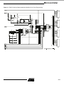
Figure 2 shows the application modified for in-circuit
programming.
It is assumed that the programmer, when inactive, will neither drive nor excessively load the application.
Since the application does not use external program memory, EA/VPP on the controller is connected to VCC . This
meets the requirement for programming.
The reset circuit has been modified by the addition of two
transistors, which allow RST on the controller to be forced
high by the programmer.
PSEN and ALE/PROG, unused in the basic application, are
under the direct control of the programmer.
Programming requires programmer access to all of the four
AT89C51 I/O ports, as documented in the data sheet. The
programmer is connected directly to those controller pins
which are unused by the application, while access to pins
used by the application requires special treatment, as
explained in the following paragraphs.
The least significant four bits of the address generated by
the programmer are multiplexed onto port one of the controller with the data from the DIP switch. Note that the four
resistors added at the switch are not required in the basic
application, since the AT89C51 provides internal pull-ups
on port one.
During the normal operation of the application, controller
ports zero and two provide data and control signals
(respectively) to the displays. During programming and program verification, the programmer asserts control of port
zero and part of port two. The programmer is connected to
ports zero and two without buffering, since, when inactive,
its presence does not affect the normal operation of the
application.
5-12
Microcontroller
A transparent latch has been added between port two of
the controller and the display control inputs. The latch holds
the display control signals inactive during programming,
which eliminates erratic operation of the displays due to
programmer activity on ports zero and two. No isolation of
the display data inputs is required, since data applied to the
inputs is ignored when the control signals are inactive.
The AT89C51 reset circuit, input multiplexer and output
latch are controlled by a single signal generated by the programmer. During programming, reset is asserted, the multiplexer switches inputs, and the latch freezes the display
control lines.
To ensure that the display control lines are in a known state
before they are latched, an AT89C51 external interrupt is
used to allow the programmer to signal the application
before asserting reset. The application firmware responds
to the interrupt by displaying a message and deactivating
the display control lines.
After programming, when reset is deasserted, the controller
ports are high as the latch becomes transparent. Since the
display control inputs are inactive high, the display contents
are not disturbed until the new program writes the display.
Although not essential to this application, it might be imperative in some applications that the state of the peripheral
circuitry not be disturbed during programming.
The Programmer
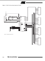
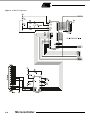
The programmer (Figure 3) generates the addresses, data
and control signals necessary to program the AT89C51
embedded in the application.
The programmer circuitry consists of an AT89C51 and an
RS-232 level translator. The controller runs at 11.0592
MHz, which allows the serial port to operate at a number of
standard baud rates. A Maxim MAX232 line driver/receiver
produces RS-232 levels at the serial interface while requiring only a five volt supply.
Many of the signals generated by the programmer are connected directly, without buffering, to the AT89C51 in the
application. These signals, when inactive, are not threestated, but are pulled high. The AT89C51 has internal pullups of approximately three Kohms on ports one, two and
three. Because port zero does not have internal pull-ups,
external pull-ups of ten Kohms have been added to permit
proper operation of program verification mode. The sample
application operates correctly in this environment. If
required for compatibility with an application, programmer
signals may be buffered with three-state buffers similar to
the 74xx125.
The AT89C51 in the programmer does not utilize external
program or data memory, which would require sacrificing
needed I/O pins. This requires that program code and I/O
buffers be kept small enough to fit in on-chip memory.