1
Errata Sheet
V1.1, 2005-12-19
Device
XC164CM-8F20F, -8F40F, -4F20F, -4F40F
Marking/Step
Step (E)ES-AA, AA
Package
PG-TQFP-64
This Errata Sheet describes the deviations from the current user documentation.
The module oriented classification and numbering system uses an ascending sequence
over several derivatives, including already solved deviations. So gaps inside this
enumeration can occur.
This Errata Sheet applies to all temperature (SAB-/SAF-/SAK-.....) and frequency
versions (.20./.40.), unless explicitly noted otherwise.
Current Documentation
•
•
•
•
XC164CM Data Sheet V1.1, 2005-11
XC164CM User's Manual V1.1, Volume 1: System Units, 2005-11
XC164CM User's Manual V1.1, Volume 2: Peripheral Units, 2005-11
C166S V2 User's Manual (Core, Instruction Set) V1.7, 2001-01
(after following a link listed above, the respective document can be found in the folder
'Documents’)
Note: Devices additionally marked with EES- or ES- or E followed by a 3-digit date code
are engineering samples which may not be completely tested in all functional and
electrical characteristics, therefore they should be used for evaluation only. The
specific test conditions for EES and ES are documented in a separate Status
Sheet.
Note: For simplicity all versions are referred to by the term XC164CM-8F, -4F throughout
this document
Contents
Section . . . . . . . . . . . . . . . . . . . . . . . . . . . . . . . . . . . . . . . . . . . . . . . . . . . . . . . . . . Page
History List/Change Summary . . . . . . . . . . . . . . . . . . . . . . . . . . . . . . . . . . . . . . . . . .2
Functional Problems . . . . . . . . . . . . . . . . . . . . . . . . . . . . . . . . . . . . . . . . . . . . . . . . . .5
OCDS and OCE Modules . . . . . . . . . . . . . . . . . . . . . . . . . . . . . . . . . . . . . . . . . . . . . .16
Deviations from Electrical- and Timing Specification. . . . . . . . . . . . . . . . . . . . . . .18
Application Hints . . . . . . . . . . . . . . . . . . . . . . . . . . . . . . . . . . . . . . . . . . . . . . . . . . . .19
Documentation Update . . . . . . . . . . . . . . . . . . . . . . . . . . . . . . . . . . . . . . . . . . . . . . .32
XC164CM-8F, -4F, Step (E)ES-AA, AA
1/32
Sa/Es/Me, V1.1, 2005-12-19
Errata Sheet
History List/Change Summary
1
History List/Change Summary
Table 1
Functional Deviations
Functional
Problem
Short Description
CPU_X.002
Branch to wrong target after mispredicted JMPI
SCU_X.011.1
Register Security Mechanism after Write Access
in Secured Mode
TwinCAN_X.007
Transmit after error
TwinCAN_X.008
Double remote request
TwinCAN_X.009
CPUUPD remote
TwinCAN_X.010
Reserved Bits in Register MSGARHn[15:13]
FLASH_X.004
PACER trap after wake-up from Sleep/Idle mode
FLASH_X.005
Logical Sector 4 Erase
ASC_X.001
ASC Autobaud Detection in 8-bit Modes with
Parity
RTC_X.002
RTC Reset after any Reset
new
PORTS_X.011
Internal Pull-Ups for Boot Configuration
new
BSL_X.002
Software or Watchdog Timer Reset in Bootstrap
Loader Mode
new
IDCHIP_X.001
IDCHIP Register contains incorrect Chip ID
new
Table 2
Fixed Change
in step
update
new
new
OCDS and OCE Modules
Functional
Problem
Short Description
OCDS_X.002
OCDS indicates incorrect status after break_now
requests if PSW.ILVL ≥ CMCTR.LEVEL
OCE_X.001
Wrong MAC Flags are declared valid at Core OCE interface
XC164CM-8F, -4F, Step (E)ES-AA, AA
Fixed Change
in step
2/32
Sa/Es/Me, V1.1, 2005-12-19
Errata Sheet
History List/Change Summary
Table 3
AC/DC Deviations
AC/DC
Deviations
Short Description
Fixed
Change
in step
No deviations from the specification are currently known
Table 4
Application Hints
Hint
Short Description
Change
CPU_X.H1
Configuration of Registers CPUCON1 and CPUCON2
CPU_X.H2
Special Characteristics of I/O Areas
FLASH_X.H1.1
Access to Flash Module after Program/Erase
FLASH_X.H2.2
Access to Flash Module after Shut-Down
FLASH_X.H3.2
Read Access to internal Flash Module with modified
Margin Level
FLASH_X.H4
Minimum active time after wake-up from sleep or idle
mode
SLEEP_X.H3.2
Clock system after wake-up from Sleep Mode
IDLE_X.H1
Entering Idle Mode after Flash Program/Erase
ADC_X.H1
Polling of Bit ADBSY
BREAK_X.H1
Break on MUL/DIV followed by zero-cycle jump
update
POWER_X.H1.1 Initialization of SYSCON3 for Power Saving Modes
POWER_X.H2.2 Power Consumption during Clock System Configuration
SCU_X.H1.1
Shutdown handshake by software reset (SRST)
instruction
SCU_X.H3
Effect of PLLODIV on Duty Cycle of CLKOUT
SCU_X.H4
Changing PLLCON in Emergency Mode
SCU_X.H5
Sleep/Idle/Power Down Mode not entered while PLLODIV
= 0FH
SCU_X.H6
Interrupt request during entry into sleep mode
SCU_X.H7
VCO Configuration with Input Clock disconnected
new
SCU_X.H8
PLL Bypass Mode with VCO on
new
FOCON_X.H1
Read Access to register FOCON
XC164CM-8F, -4F, Step (E)ES-AA, AA
3/32
Sa/Es/Me, V1.1, 2005-12-19
Errata Sheet
History List/Change Summary
Table 4
Application Hints (cont’d)
Hint
Short Description
RTC_X.H1.3
Disabling of the Real Time Clock
RTC_X.H2
RTC_CON Reset Value
TwinCAN_X.H2
Reading Bitfield INTID
INT_X.H1
Software Modifications of Interrupt Enable (xx_IE) or
Interrupt Request (xx_IR) Flags
Table 5
Name
Change
new
new
Documentation Update
Short Description
Change
No topics for documentation updates are currently known
XC164CM-8F, -4F, Step (E)ES-AA, AA
4/32
Sa/Es/Me, V1.1, 2005-12-19
Errata Sheet
Functional Problems
2
Functional Problems
CPU_X.002 Branch to wrong target after mispredicted JMPI
After a JMPI is initially mispredicted according to the static branch prediction scheme of
the C166S V2, code execution may continue at a wrong target address in the following
situations:
Situation I:
• a memory write operation is processed by the DMU
• followed by a MUL(U)
• followed by the mispredicted JMPI
Example_1:
MOV mem, [Rwn]
MUL R13, R14
JMPI cc_NV, [R6]
Situation II:
• MUL(U) or DIV(L/U/LU)
• followed by not-mispredicted zero-cycle jump
(e.g. JMPA, JMPR, JMPS; bit ZCJ (CPUCON1.0) = 1)
• followed by the mispredicted JMPI
Example_2a:
MULU R13, R14
JMPA- cc_V, _some_target
JMPI cc_NV, [R6]
; predicated not taken => correct
; taken, but predicted not taken
It could be possible that the JMPI is at the jump target of the JMPA, if it is taken:
Example_2b:
MULU R13, R14
JMPA+ cc_NZ, _jmpi_addr
; predicted taken => correct
..... other code ....
_jmpi_addr: JMPI cc_NV, [R6] ; taken but predicted not taken
Effect on tools:
In the Altium/Tasking compiler (V7.0 and above) the problem is not present. The result
of a MUL/DIV instruction is available through the MDL/MDH SFRs. These SFRs are not
allocatable by the register allocator. Therefore, the compiler always needs a MOV
instruction to transfer MDL/H to a GPR. This avoids the problem.
XC164CM-8F, -4F, Step (E)ES-AA, AA
5/32
Sa/Es/Me, V1.1, 2005-12-19
Errata Sheet
Functional Problems
In the RT- and FP-libraries (v7.0 and above) the problem was not found. Versions lower
than v7.0 do not explicitly support the C166S V2 core.
In case optimizations are implemented in future versions which could cause this problem
to occur, also a workaround will be included.
All Keil C166 tool Versions (compiler and libraries) since V3.xx do not generate a
MUL(U) or a DIV(L/U/LU) followed by either of the jump instructions JMPR, JMPS,
JMPA, JMPI. Basically the support of the C166S V2 core requires anyway V4.21 or
higher.
Workarounds:
Examples for program parts written in assembly language:
• generally disable overrun of pipeline bubbles by clearing bit CPUCON2.OVRUN
(CPUCON2.4 = 0). This will result only in a negligible performance decrease, and will
prohibit corruption of the target IP of the JMPI.
or:
• provide a NOP (or any other suitable instruction) between the MUL/DIV instructions
and the succeeding jump in the above cases. To simplify, place a NOP between any
MUL/DIV and a JMPR, JMPS, JMPA, JMPI that might follow it. Other branches
(CALLs, jump-on-bit instructions) do not need to be taken into account.
SCU_X.011.1 Register Security Mechanism after Write Access in Secured Mode
To modify an SFR that is protected by the register security mechanism, a certain security
level has to be selected and/or a command sequence has to be executed prior to the
write access to one of these registers. Table 6-15 in the User’s Manual, volume System
Units, lists all registers protected by the security mechanism (see copy of Table 6-15
below).
After selecting Secured Mode (bitfield SL = 01B in register SCUSLS), a single command
(command4) enables one single write access to a protected register. After this write
access the protected registers are locked again automatically.
Exception:
After modification of registers CPUCON1, CPUCON2, TCONCS7, FCONCS7,
ADDRSEL7 (which are not part of the SCU), all registers listed in Table 6-15 are not
locked until the next write access to an SCU register (i.e. a register which is different
from the group CPUCON1 .. ADDRSEL7).
XC164CM-8F, -4F, Step (E)ES-AA, AA
6/32
Sa/Es/Me, V1.1, 2005-12-19
Errata Sheet
Functional Problems
Workaround:
In order to lock all registers again, after a write access to the non-SCU registers
CPUCON1 .. ADDRSEL7 a "dummy" write access to an SCU register should be
executed. It is therefore proposed to use e.g. the read-only register IDCHIP for this
purpose. The registers of the identification control block also belong to the SCU, and a
write access to these read-only registers re-enables secured mode:
Example:
MOV
EXTR
MOV
OR
MOV
R4, #0243H
#1
SCUSLC , #8E12H
TCONCS7, R4
IDCHIP , ZEROS
Table 6
;
;
;
;
;
;
value to be stored in register TCONCS7
Access sequence in secured mode
Command4: current password = EDH
Access to TCONCS7 enabled by preceding Command4
dummy write to a read-only SCU register
re-enables secured mode
Registers Protected by the Security Mechanism
Register Name
Function
Loc.
RSTCON
Reset control
SCU
SYSCON0
General system control
SCU
SYSCON1
Power management
SCU
PLLCON
Clock generation control
SCU
SYSCON3
Peripheral management
SCU
FOCON
Peripheral management (CLKOUT/FOUT)
SCU
IMBCTR
Control of internal instruction memory block
SCU
OPSEN
Emulation control
SCU
EMUCON
Emulation control
SCU
WDTCON
Watchdog timer properties
SCU
EXICON
Ext. interrupt control
SCU
EXISEL0, EXISEL1
Ext. interrupt control
SCU
CPUCON1, CPUCON2
CPU configuration
CPU
TCONCS7
EBC timing configuration
EBC
FCONCS7
EBC function configuration
EBC
ADDRSEL7
EBC address window configuration
EBC
XC164CM-8F, -4F, Step (E)ES-AA, AA
7/32
Sa/Es/Me, V1.1, 2005-12-19
Errata Sheet
Functional Problems
TwinCAN_X.007 Transmit after Error
During a CAN error, transmission may stop (after EOF or an error frame), until a
successful reception or a write access to the TwinCAN module.
Detailed Description
In case of a CAN error and when there is no other activity on the CAN module (e.g. frame
reception or frame transmission on the other CAN node or write access to any CAN
register), the transmission of messages may stop, even if some transmit requests are
still set.
The CAN module will start transmitting immediately, after a reception or a write access
to the module.
Workarounds:
• Write periodically FFFFH to one of the MSGCTRx registers, as this value is having no
effect on the register.
• In case writing to a CAN register shall be the exception, use the last error code (LEC)
interrupt. This shall start writing to one of the MSGCTRx register FFFFH, in case the
LEC value is unequal to 0.
TwinCAN_X.008 Double remote request
After the transmission of the remote request, TXRQ is not cleared in the receive object,
if NEWDAT is set. As a consequence the remote request is transmitted once again.
Workaround:
Clear NEWDAT after the reception of a data frame.
TwinCAN_X.009 CPUUPD remote
In case of a remote request to a standard message object which is chosen for
transmission, a transmit of the data frame takes place, even if CPUUPD is currently set.
Detailed Description
If a transmit message object gets a remote request and there is no other message object
with higher transmit priority pending for transmission, then the transmit object sends the
data frame to answer the remote request, even if CPUUPD is set.
XC164CM-8F, -4F, Step (E)ES-AA, AA
8/32
Sa/Es/Me, V1.1, 2005-12-19
Errata Sheet
Functional Problems
Workaround:
This workaround is only required in systems where remote requests are used.
To answer remote requests, the MMC bitfield in MSGFGCR has to be configured to a
FIFO slave object instead of a standard message object for transmission. To reach this
goal, the following settings for the corresponding message object are needed:
• bitfield MMC (MSGFGCRHn.10-8) = 011B (FIFO functionality enabled (slave object))
• bitfield CANPTR (MSGFGCRHn.4-0) = n (the CAN Pointer shall reference itself, by
referring to the message object number of this object)
• bit FD (MSGFGCRLn.13) = 0 (the CANPTR is updated after a correct reception)
TwinCAN_X.010 Reserved Bits in Register MSGARHn[15:13]
The 3 reserved bits MSGARHn[15:13] in the Message Object n Arbitration Register may
be erroneously loaded with non-zero values (i.e. different from their reset values) under
an arbitration loss condition.
Workaround:
If the received identifier is checked by software, the software should be written in a way
that these bits have no impact on the decision (e.g. by masking off the upper 3 bits).
FLASH_X.004 PACER Trap after Wake-Up from Sleep/Idle Mode
An unexpected Program Access Error Trap (flag PACER = 1 in register TFR) occurs
after a wake-up event from sleep or idle mode under the following conditions:
• bit field PFCFG = 01B in register SYSCON1, i.e. the flash module is switched off
during sleep or idle mode
• a wake-up event (interrupt, PEC transfer, NMI) occurs in a specific time window (few
clock cycles) after execution of the IDLE instruction during the flash deactivation
process
• and the corresponding interrupt/trap routine or the instruction following IDLE (in case
interrupts are disabled) or the PEC source data are located in the internal flash.
Workaround 1:
Do not switch off the flash module in sleep or idle mode, i.e. leave bit field PFCFG = 00B
in register SYSCON1 (default after reset). This increases power consumption to a
certain extent while reducing the time overhead for sleep/idle mode entry and exit (in
clocking modes where the clock is derived from the VCO).
XC164CM-8F, -4F, Step (E)ES-AA, AA
9/32
Sa/Es/Me, V1.1, 2005-12-19
Errata Sheet
Functional Problems
Workaround 2
In order to avoid the problem (when PFCFG = 01B), make sure that the wake-up trigger
only occurs after the device has completely entered sleep or idle mode.
If the RTC is used as wake-up source, check e.g. the RTC before entering sleep mode.
If the wake-up trigger will occur soon, either skip entry into sleep mode, or extend the
time for the next wake-up. If the RTC time interval is reprogrammed, make sure that no
interrupt occurs between reprogramming and entry into sleep mode.
Workaround 3
In order to differentiate an unexpected PACER trap due to a wake-up trigger in the critical
time window from other events that can lead to a PACER trap, set a semaphore bit
before executing the IDLE instruction., e.g.
ATOMIC #2
BSET
sema_idle
IDLE
In the trap handler for the PACER trap, if the semaphore bit is set and no other
indications for the PACER trap are found (e.g. error flags in register FSR are set), clear
the semaphore bit and the PACER flag and return from the trap handler with RETI. The
stack contains a valid return address in this case (e.g. address of instruction following
IDLE in case interrupts were disabled during wake-up).
For PEC transfers during sleep or idle mode, which will cause a PACER trap if they read
data from flash, automatic return to sleep/idle mode is not accomplished with the concept
described so far.
• In order to support return to idle/sleep mode after a PEC transfer (which is performed
after the RETI instruction from the PACER trap routine is executed), e.g. a semaphore
bit may be used. This bit may be set to '1' before the IDLE instruction is executed. All
trap (except PACER) and interrupt service routines invoked after wake up from idle/
sleep should clear this bit to '0'. After having returned from the PACER trap routine to
the program in the internal flash, this bit should be tested (allow a sufficient time of e.g.
12 cycles for interrupt arbitration), and if it is still at '1' (i.e. no interrupts/traps have
occurred), repeat the IDLE instruction for re-entry into idle/sleep mode.
Workaround 4
Use an auxiliary sequence in internal PRAM that bridges the time until the flash is ready
after wake-up from sleep/idle mode, e.g.:
• Disable interrupts, and execute the IDLE instruction to enter sleep mode from the
internal PRAM. After wake-up, the instruction following IDLE will be executed (if no
hardware trap or NMI has occurred).
XC164CM-8F, -4F, Step (E)ES-AA, AA
10/32
Sa/Es/Me, V1.1, 2005-12-19
Errata Sheet
Functional Problems
• Wait until the internal flash is ready after wake-up (check register FSR) before reading
from the internal flash). If the sequence in internal PRAM that includes the IDLE
instruction is not CALLed from internal flash (i.e. it is not terminated with a RETx
instruction), at least 8 instructions that do not read from the internal flash should be
inserted after the IDLE instruction to avoid speculative prefetches
• Enable the interrupt system again.
The following details should be considered:
• If hardware traps (including NMI) can occur, add the corresponding interrupt vectors
to PRAM and modify register VECSEG to point to the PRAM space.
• In order to support return to idle/sleep mode after a PEC transfer, e.g. a semaphore
bit may be used. This bit may be set to '1' before the IDLE instruction is executed. All
trap and interrupt service routines invoked after wake up from idle/sleep should clear
this bit to '0'. After having returned to the program in the internal flash and having
enabled the interrupt system, this bit should be tested (allow a sufficient time of e.g.
12 cycles for interrupt arbitration), and if it is still at '1' (i.e. no interrupts/traps have
occurred), repeat the auxiliary routine that prepares for re-entry into idle/sleep mode.
FLASH_X.005 Logical Sector 4 Erase
An erase operation of the logical sector 4 (32Kbyte sector from C0:8000H.. C0:FFFFH)
may fail when the master clock frequency exceeds 10MHz. Typically, the problem is
more likely to occur under the following external conditions:
• The voltage VDDI is above its nominal value (i.e. >2.5V).
• The voltage VDDP is below its nominal value (i.e. <5.0V).
• The ambient temperature is above room temperature (i.e. >25°C).
However, it can not be excluded that this problem does not occur outside the
temperature and voltage ranges listed above.
An erase operation of a wordline in logical sector 4 does always work. Thus this
operation can be done under all conditions without decreasing the master clock
frequency and without a second erase operation (see workaround below).
Workarounds:
1. Do the erase logical sector 4 operation twice:
Example code:
MOV
MOV
MOV
R4 , #0080h
R5 , #00AAh
R6 , #0033h
CALL waitBusy
EXTS #0C0h , #3
; data for 1st erase command
; data for 2nd erase command
; data for 3rd erase command
; before erase operation check if flash is busy
; use segment 0C0h for next 3 operations
XC164CM-8F, -4F, Step (E)ES-AA, AA
11/32
Sa/Es/Me, V1.1, 2005-12-19
Errata Sheet
Functional Problems
MOV
MOV
MOV
000AAh , R4
00054h , R5
08000h , R6
CALL waitBusy
EXTS
MOV
MOV
MOV
#0C0h
000AAh
00054h
08000h
,
,
,
,
#3
R4
R5
R6
;
;
;
;
;
1st erase command
2nd erase command
3rd erase command to
logical sector 4 at 08000h
wait until erase operation is done
;
;
;
;
;
use
1st
2nd
3rd
for
segment 0C0h for next 3 operations
erase command
erase command
erase command
logical sector 4 at 08000h
CALL waitBusy
... further code
; subroutine to wait for busy
waitBusy:
EXTS #0FFh, #1
MOV R7
, 0F000h
JB
R7.0 , waitBusy
RET
signal
; check busy flag in FSR
; use segment 0FFh for next operation
; read FSR
; if flash still busy loop again
2. Reduce the master clock frequency below 10MHz:
Example code:
PLLCON_VAL
equ XXXX
; XXXX must yield a frequency below 10MHz
MOV R4
, #PLLCON_VAL
MOV PLLCON, R4
pllconWait:
MOV R5
, PLLCON
CMP R5
, R4
JMP cc_NE , pllconWait
; reconfigure PLLCON
MOV
MOV
MOV
R4 , #0080h
R5 , #00AAh
R6 , #0033h
; data for 1st erase command
; data for 2nd erase command
; data for 3rd erase command
CALL
EXTS
MOV
MOV
MOV
waitBusy
#0C0h ,
000AAh ,
00054h ,
08000h ,
#3
R4
R5
R6
; wait until PLLCON configuration is done
; before erase operation check if flash is busy
; use segment 0C0h for next 3 operations
; 1st erase command
; 2nd erase command
; 3rd erase command to
; for logical sector 4 at 08000h
CALL waitBusy
XC164CM-8F, -4F, Step (E)ES-AA, AA
12/32
Sa/Es/Me, V1.1, 2005-12-19
Errata Sheet
Functional Problems
... further code
; subroutine to wait for busy signal
waitBusy:
; check busy flag of FSR
EXTS #0FFh, #1
; use segment 0FFh for next operation
MOV R7
, 0F000h
; read FSR
JB
R7.0 , waitBusy
; if flash still busy loop again
RET
Any erase operation takes about 110ms. The time for an erase operation is almost
independent of the master clock frequency. Thus the second workaround is faster.
ASC_X.001 ASC Autobaud Detection in 8-bit Modes with Parity
The Autobaud Detection feature of the Asynchronous/Synchronous Serial Interface
(ASC) does not work correctly for 8-bit modes with even or odd parity.
The Autobaud Detection feature works correctly for 7-bit modes with even or odd parity,
and for 8-bit modes without parity.
RTC_X.002: RTC Reset after any Reset
When the device is reset using a software reset, a watchdog timer reset or a hardware
reset, the RTC module is also reset. The RTC time is set to zero.
Workaround:
Store the RTC timer contents in regular time intervals e.g. in internal RAM and use the
stored values to restore the contents of the RTC timer registers after the reset. When the
device is reset in a controled way by the user software, i.e. by a software reset, the RTC
time can be stored to the internal RAM directly before the reset is applied. To increase
the accuracy of this method the time that is typical for the internal reset sequence with
the applied settings can be added to the restored RTC value.
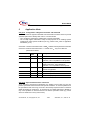
PORTS_X.011 Internal Pull-Ups for Boot Configuration
After a hardware reset and during the internal reset phase the internal pull-ups of the
boot configuration pins P9.4/5 and P1H.4/5 may not manage to generate a voltage level
that can be recognized as a logic 1. Instead, external pull-ups must be provided to latch
the intended levels of the boot configuration pins P9.4/5 and P1H.4/5 at the end of the
internal reset phase. Table 7 shows the necessary external pull-up and pull-down
combinations for different boot modes.
XC164CM-8F, -4F, Step (E)ES-AA, AA
13/32
Sa/Es/Me, V1.1, 2005-12-19
Errata Sheet
Functional Problems
Table 7
External Pull-Up/-Down Configurations for different Boot Modes
Boot mode
TRST
P9.4
P9.5
P1H.4
P1H.5
internal start
PD1)
X2)
X
X
X
internal start with OCDS
enabled3)
PU4)
PU
PU
X
X
ASC boot
PU
PU
PD
X
X
Adapt mode
PU
PD
PD
PU
PU
1)
Pull-Down
2)
Don’t care
In XC164CM this mode is used for start from internal memory at C0.0000H in conjunction with OCDS. Standard
start from internal memory at C0.0000H is always performed if TRST=0 during reset.
3)
4)
Pull-Up
Note: If the test reset pin is inactive, i.e. TRST=1, then the internal pull-ups of the boot
configuration pins are active during the internal reset phase. Hence the internal
pull-up resistors must be considered if an external pull-up or an external pull-down
shall be connected to a boot configuration pin. For further information see the
respective data sheet.
BSL_X.002 Software or Watchdog Timer Reset in Bootstrap Loader Mode
When bootstrap loader mode was entered upon the last hardware reset, and a software
or watchdog timer reset is performed by the loaded program, code execution will not start
at location C0’0000H in the internal program flash. Instead, the device returns into
bootstrap loader mode, waiting for a zero byte at pin RxD0.
Workaround 1:
To exit bootstrap loader mode, perform a hardware reset with an external configuration
that does not select bootstrap loader mode, i.e. either with
• TRST = low, or
• TRST = high and P9.4 = high and P9.5 = high (see also PORTS_X.011)
Workaround 2:
To exit bootstrap loader mode, emulate the effects of a reset by software, i.e.
• initialize registers that were used by the bootstrap loader either with their default
values or as required by the application (see table in User’s Manual, chapter 10.1)
• initialize DPP0..3 to 0..3
• set VECSEG = 0C0h
XC164CM-8F, -4F, Step (E)ES-AA, AA
14/32
Sa/Es/Me, V1.1, 2005-12-19
Errata Sheet
Functional Problems
• enable the watchdog timer
• execute a JMPS 0C0h, 0000h to the internal program flash
IDCHIP_X.001: IDCHIP Register contains incorrect Chip ID
The IDCHIP register contains 2301H instead of 2381H. To distinguish a XC164CM
device from other XC166 derivatives use the IDCHIP register in combination with the
IDMEM register.
Table 8
XC164CM Identification Registers
Step
Register:
IDCHIP
IDMEM
Address:
FO7CH
F07AH
XC164CM-4FF
AA
2301H
3010H
XC164CM-8FF
AA
2301H
3010H
XC164CM-8F, -4F, Step (E)ES-AA, AA
15/32
Sa/Es/Me, V1.1, 2005-12-19
Errata Sheet
OCDS and OCE Modules
3
OCDS and OCE Modules
The following issues have been found in the OCDS and OCE modules. Please see the
debugger or emulator manufacturer's documentation whether or not these issues
actually cause a problem or restriction when the respective tool is used.
OCDS_X.002 OCDS indicates incorrect status after break_now requests if
PSW.ILVL ≥ CMCTR.LEVEL
When the OCDS processes a break_now request while the CPU priority level (in
PSW.ILVL) is not lower than the OCDS break level (in CMCTR.LEVEL), the actual break
is delayed until either PSW.ILVL or CMCTR.LEVEL is reprogrammed such that
CMCTR.LEVEL > PSW.ILVL. If in the meantime further debug events have occurred,
register DBGSR will still indicate the status of the first break_now request. If e.g. a
software break is executed, the OCDS will accept this, but register DBGSR will indicate
the wrong cause of break.
Workarounds:
1. If the application uses tasks with different levels and debugging is to take place using
the OCDS break level feature (e.g. only tasks up to a maximum level are halted,
higher-level tasks aren't halted, and the OCDS level is programmed in between), there
is no problem if:
• only classic hardware breakpoints (IP address) or software breakpoints are used (i.e.
no trigger on address, data, TASKID)
• no external pin assertions are used to trigger breaks
• no direct writes to DBGSR.DEBUG_STATE are used to force breaks
2. If break_now request sources are to be used, the maximum level of the application
(PSW.ILVL) should always be lower than the programmed OCDS break level (e.g.
PSW.ILVL ≤ 14D and CMCTR.LEVEL = 15D). This means that all generated
break_now requests by the OCDS will always be accepted, independent of the CPU
or interrupt priority.
OCE_X.001 Wrong MAC Flags are declared valid at Core - OCE interface
In case a MAC instruction (Co...) is directly followed by a MOV MSW, #data16
instruction, the upper byte of data16 is output instead of the flags corresponding to the
MAC instruction. The bug was found with code:
COSHR
MOV
#00001h
MSW, #00100h
;(+ other variations of data16)
XC164CM-8F, -4F, Step (E)ES-AA, AA
16/32
Sa/Es/Me, V1.1, 2005-12-19
Errata Sheet
OCDS and OCE Modules
Workaround
Add a NOP instruction between the two instructions:
COSHR
NOP
MOV
#00001h
MSW, #00100h
;(+ other variations of data16)
XC164CM-8F, -4F, Step (E)ES-AA, AA
17/32
Sa/Es/Me, V1.1, 2005-12-19
Errata Sheet
Deviations from Electrical- and Timing Specification
4
Deviations from Electrical- and Timing Specification
No deviations from the specification are currently known.
XC164CM-8F, -4F, Step (E)ES-AA, AA
18/32
Sa/Es/Me, V1.1, 2005-12-19
Errata Sheet
Application Hints
5
Application Hints
CPU_X.H1 Configuration of Registers CPUCON1 and CPUCON2
The default values of registers CPUCON1 and CPUCON2 have been chosen to provide
optimized performance directly after reset. It is recommended
• not to modify the performance related parts of register CPUCON1
• not to modify register CPUCON2, except for test purposes or for enabling specific
workarounds under special conditions (see e.g. problem CPU_X.002 or application
hint BREAK_X.H1).
CPUCON2: reset/recommended value = 8FBBH; enables several performance features
CPUCON1: reset/recommended value = 0..0 0XXX X111B ; only the 3 LSBs are
performance related
Bit Position
Field
Name
Value Description
CPUCON1.[15:7] 0
0
reserved
CPUCON1.[6:5]
VECSC
00
scaling factor for vector table, value depends on
application, '00' is compatible to C166 systems
CPUCON1.4
WDTCTL 0
configuration for scope and function of DISWDT/
ENWDT instructions, value depends on
application, '0' is compatible to C166 systems
CPUCON1.3
SGTDIS
segmentation enable/disable control, value
depends on application
CPUCON1.2
INTSCXT 1
enable interruptibility of switch context
CPUCON1.1
BP
1
enable branch prediction unit
CPUCON1.0
ZCJ
1
enable zero cycle jump function
0
CPU_X.H2 Special Characteristics of I/O Areas
As an element of performance optimization, the pipeline of the C166S V2 core may
perform speculative read accesses under specific conditions. In case the prediction for
the speculative read was wrong, the read to the actually required location is restarted.
While this method is uncritical e.g. for accesses to non-volatile memories or SRAMs, it
may cause problems on devices which do not tolerate speculative reads (e.g. FIFOs
which are advanced on every read access).
XC164CM-8F, -4F, Step (E)ES-AA, AA
19/32
Sa/Es/Me, V1.1, 2005-12-19
Errata Sheet
Application Hints
No speculative reads are performed in memory areas which are marked as I/O area.
This memory area includes
• the SFR and ESFR space (e.g. with buffers for received data from serial interfaces or
A/D results)
• the 4 Kbyte internal I/O area (00'E000H ..00'EFFFH), including IIC1) and SDLM1)
module
• the 2 Mbyte external I/O area (20'0000H ..3F'FFFFH), including the TwinCAN1)
module (default: from 20'0000H .. 20'07FFH)
It is therefore recommended to map devices which do not tolerate speculative reads into
the 2 Mbyte external I/O area (20'0000H ..3F'FFFFH).
For further special properties of the I/O areas, see section IO Areas (3.6) in chapter
Memory Organization in the User's Manual.
FLASH_X.H1.1 Access to Flash Module after Program/Erase
After the last instruction of a program or erase command, the BUSY bit in register FSR
is set to '1' (status = busy) after a delay of one instruction cycle. When polling the BUSY
flag, one NOP or other instruction which is not evaluating the BUSY flag must be inserted
after the last instruction of a program or erase command.
No additional delay is required when performing the first operand read or instruction
fetch access from the flash module after the BUSY bit has returned to '0' (status = not
busy).
FLASH_X.H2.2 Access to Flash Module after Shut-Down
When the flash is disabled by software (shut-down) by writing bit PFMDIS = 1 in register
SYSCON3,
• and it is (at some later time) enabled again by writing PFMDIS = 0
• and the instruction immediately following the instruction which sets PFMDIS = 0 is
fetched or reads operands from internal flash
then the PACER flag in register TFR is set and the BTRAP routine is entered.
Therefore, it is recommended to insert 4 NOPs before the internal flash is accessed
again after PFMDIS has been set to 0.
1)
this module is implemented in specific derivatives of the XC166 family
XC164CM-8F, -4F, Step (E)ES-AA, AA
20/32
Sa/Es/Me, V1.1, 2005-12-19
Errata Sheet
Application Hints
FLASH_X.H3.2 Read Access to internal Flash Module with modified Margin Level
When the internal flash module is read (e.g. for test purposes) with modified margin level
(i.e. bitfield MARLEVSEL = 0001B or 0100B) in register MAR, an additional wait state
must be selected in bitfield WSFLASH in register IMBCTR. This waitstate must be added
to the number of flash waitstates that are required to match the flash access time to the
CPU operating frequency.
FLASH_X.H4 Minimum active time after wake-up from sleep or idle mode
If the flash module is automatically disabled upon entry into sleep or idle mode (bit field
PFCFG = 01B in register SYSCON1), sleep or idle mode should not be re-entered before
a minimum active ("awake") time has elapsed. Otherwise, the current consumption
during this sleep/idle phase will be ~ 1 mA above the specified limits of the Data Sheet.
Therefore,
• If code is executed from the internal flash after wake-up, at least 16 instructions
should be executed from the internal flash before re-entering sleep/idle mode. This
ensures that the flash module is actually accessed after wake-up, since more
instructions are required than can be stored in the prefetch queue.
• If code is executed from external memory or PRAM, wait until the flash BUSY bit
returns to '0' before re-entering sleep/idle mode.
• If PEC transfers with automatic return to sleep/idle mode shall be triggered by the
wake-up event, use e.g. the following procedure:
Use an auxiliary routine in internal flash with the required minimum active time after
wake-up from sleep or idle mode, e.g.
– define a semaphore bit that is set to '1' before the IDLE instruction is executed. All
trap and interrupt service routines invoked after wake up from idle/sleep should
clear this bit to '0'
– disable interrupts
– execute the IDLE instruction
– if idle or sleep mode is terminated by an interrupt request, the instructions following
the IDLE instruction will be executed (the interrupt request flags remain set)
– if idle or sleep mode was terminated by an NMI, the trap handler will be invoked
– enable interrupts to allow prioritization of requests for interrupt or PEC service
– the instructions following the IDLE instruction should test the flash BUSY bit in
register FSR; when the flash is ready (BUSY = 0), and at least 12 instructions have
been executed after the interrupt system has been enabled, and if the semaphore
bit is still at '1' (i.e. no interrupts/traps have occurred), disable interrupts and return
to the IDLE instruction.
XC164CM-8F, -4F, Step (E)ES-AA, AA
21/32
Sa/Es/Me, V1.1, 2005-12-19
Errata Sheet
Application Hints
SLEEP_X.H3.2 Clock system after wake-up from Sleep Mode
There are different wake-up behaviors, depending on the PLL control setting used in
register PLLCON during entry into sleep mode, and depending on whether the RTC is
running on the main oscillator. Note that in either case, the VCO is turned off during sleep
mode, and does not contribute to any additional power consumption.
• In bypass mode with VCO off (PLLCTRL = 00B), the device will directly continue to
run on the frequency derived from the external oscillator input after wake-up from
sleep. If the RTC is running on the main oscillator, the device is immediately clocked,
since the oscillator (input XTAL1) is not turned off during sleep mode.
If the RTC was not running on the main oscillator, the system will not be clocked until
the amplitude on the external oscillator input XTAL1 exceeds the input hysteresis.
This requires typ. a few ms, depending on external crystal/oscillator circuit.
With this mode, there is no oscillator watchdog function, and the system will not be
clocked until the external oscillator input XTAL1 receives a clock that exceeds the
input hysteresis.
• In bypass mode with VCO on (PLLCTRL = 01B), the device will directly continue to
run on the frequency derived from the external oscillator input after wake-up from
sleep if the RTC continues to run on the main oscillator in sleep mode.
In case the PLL was locked before entry into sleep mode, emergency mode is
entered. This results in PLLODIV = 0FH and bit SYSSTAT.EM = 1. This change of
configuration will not be notified by the PLL Unlock/OWD interrupt (flag PLLIR). This
condition will remain until an external HW reset is applied, or a wake-up event from
sleep mode with main oscillator off (i.e. RTC not running on main oscillator) occurs.
If the RTC was not running on the main oscillator, (i.e. the main oscillator was off
during sleep mode), the device will wake-up using the internal PLL base frequency
from the VCO (fbase/16) and will temporarily stay in emergency mode (i.e. run on the
frequency derived from the VCO) until bit OSCLOCK in register SYSSTAT gets set
to 1.
It is not possible to switch to direct drive (VCO bypass) mode within this timeframe. If
bypass mode (PLLCTRL = 00B, i.e. no oscillator watchdog support) is required by an
application after wake-up from sleep, it is therefore recommended to switch to bypass
mode already before entry into sleep mode (check PLLCON for its target value before
executing the IDLE instruction to enter sleep mode). See also SCU_X.H5.
• In PLL mode with input clock from XTAL1 disconnected (PLLCTRL = 10B), the device
will only wake up from sleep if the RTC was not running on the main oscillator (i.e.
XC164CM-8F, -4F, Step (E)ES-AA, AA
22/32
Sa/Es/Me, V1.1, 2005-12-19
Errata Sheet
Application Hints
when the main oscillator is off during sleep mode). In this case, the device will run
using the internal PLL base frequency from the VCO (fbase/16) until the amplitude on
the external oscillator input XTAL1 exceeds the input hysteresis, and then switch to
fbase/k with the output divider selected by PLLODIV.
If the RTC is running on the main oscillator, the device will not wake-up from sleep
mode with this PLLCTRL setting. It is therefore recommended to switch to bypass
mode (PLLCTRL = 00B) before entry into sleep mode (check PLLCON for its target
value before executing the IDLE instruction to enter sleep mode).
• In PLL mode with input clock from XTAL1 connected to the VCO (PLLCTRL = 11B),
if the RTC was not running on the main oscillator, the device will wake-up in
emergency mode and run using the internal PLL base frequency from the VCO (fbase/
16) until the amplitude on the external oscillator input XTAL1 exceeds the input
hysteresis. Then the PLL resynchronizes to the target frequency determined by the
settings in register PLLCON. When bit OSCLOCK gets set in register SYSSTAT, the
output divider PLLODIV will be set to the target value.
If the RTC is running on the main oscillator, the device will wake-up and resynchronize
to the target frequency determined by the settings in register PLLCON.
In case the PLL was locked before entry into sleep mode, emergency mode is
entered. This results in PLLODIV = 0FH and bit SYSSTAT.EM = 1. This change of
configuration will not be notified by the PLL Unlock/OWD interrupt (flag PLLIR). This
condition will remain until an external HW reset is applied, or a wake-up event from
sleep mode with main oscillator off (i.e. RTC not running on main oscillator) occurs.
As an alternative, switch to bypass mode with VCO on and PLL unlocked before
entering sleep mode (e.g. PLLCON = 2000H). After wake-up, PLLCON may be
reconfigured to the desired PLL operating mode.
IDLE_X.H1 Entering Idle Mode after Flash Program/Erase
After a program/erase operation, idle mode should not be entered before the BUSY bit
in register FSR has returned to '0' (status = not busy).
ADC_X.H1 Polling of Bit ADBSY
After an A/D conversion is started (standard conversion by setting bit ADST = 1, injected
conversion by setting ADCRQ = 1), flag ADBSY is set 5 clock cycles later. When polling
for the end of a conversion, it is therefore recommended to check e.g. the interrupt
XC164CM-8F, -4F, Step (E)ES-AA, AA
23/32
Sa/Es/Me, V1.1, 2005-12-19
Errata Sheet
Application Hints
request flags ADC_CIC_IR (for standard conversions) or ADC_EIC_IR (for injected
conversions) instead of ADBSY.
BREAK_X.H1 Break on MUL/DIV followed by zero-cycle jump
When a MUL or DIV instruction is immediately followed by a falsely predicted conditional
zero-cycle jump (JMPR or JMPA on any condition other than cc_UC),
and
• either a 'break now' request is set at the time the MUL / DIV instruction is being
executed (i.e. a break request on operand address, data, task ID, BRKIN pin etc. is
generated by one of the instructions (may be up to four) preceding MUL/DIV)
• or a 'break-before-make' request (break on IP address) is derived from the instruction
immediately following the jump (jump target or linear following address, depending
whether the jump is taken or not )
then the internal program counter will be corrupted (equal to last value before jump),
which will lead to a false update of the IP with the next instruction modifying the IP.
This problem occurs for debugging with OCDS as well as with OCE.
Note: The Tasking and Keil compilers (including libraries) do not generate this type of
critical instruction sequence.
Workarounds (choices)
For assembler programmers, one of the following workarounds may be used
1. disable zero-cycle operation for jumps when debugging code (set CPUCON1.ZCJ to
'0'), or
2. include a NOP after any MUL/DIV instruction followed by a conditional jump (JMPR,
JMPA), or
3. do not set any 'break-before-make'-type breakpoints on the instruction following the
jump, or 'break now'-type breakpoints shortly before or on the MUL / DIV instructions
POWER_X.H1.1 Initialization of SYSCON3 for Power Saving Modes
For minimum power consumption during power saving modes, all modules which are not
required should be disabled in register SYSCON3, i.e. the corresponding disable bits
should be set to '1', including bits which are marked as 'reserved' (this provides
compatibility with future devices, since all SYSCON3 bits are disable bits). Reading
these bits will return the written value, as for peripherals without shut-down handshake.
XC164CM-8F, -4F, Step (E)ES-AA, AA
24/32
Sa/Es/Me, V1.1, 2005-12-19
Errata Sheet
Application Hints
For peripherals equipped with peripheral shut-down handshake, reading allows to check
their shut-down status.
POWER_X.H2.2 Power Consumption during Clock System Configuration
In the following situations
1. after wake-up from sleep mode until oscillator lock in case the main oscillator was
turned off during sleep mode
2. after a clock failure (PLL unlock or oscillator fail) until clock reconfiguration by software
the device is internally clocked by the VCO running on the base frequency of the
currently selected VCO band divided by 16. This results in an operating frequency range
of 1.25 .. 11.25 MHz, depending on the currently selected VCO band.
Systems designed for lower target frequencies should consider the increased power
consumption due to the potential frequency increase during these phases of operation.
Exception in bypass mode with VCO off: in case (1), if the RTC is not running on the
main oscillator, and case in (2) the device stops until it again receives a clock from the
oscillator.
SCU_X.H1.1 Shutdown handshake by software reset (SRST) instruction
In the pre-reset phase of the software reset instruction, the SCU requests a shutdown
from the active modules equipped with shutdown handshake (see section Peripheral
Shutdown Handshake (6.3.3) in chapter Central System Control Functions in the User's
Manual). The pre-reset phase is complete as soon as all modules acknowledge the
shutdown state.
As a consequence, e.g. the A/D converter will only acknowledge the request after the
current conversion is finished (fixed channel single conversion mode), or after
conversion of channel 0 (auto scan single conversion mode). If the 'Wait for Read Mode'
mode is selected (bit ADWR = 1), the ADC does not acknowledge the request if the
conversion result from register ADC_DAT has not been read.
Therefore, before the SRST instruction is executed, it is recommended e.g. in the
continuous (fixed or auto scan) conversion modes to switch to fixed channel single
conversion mode (ADM = 00B) and perform one last conversion in order to stop the ADC
in a defined way. In the auto scan conversion modes, this switch is performed after
conversion of channel 0. If a 0-to-1 transition is forced in the start bit ADST by software,
a new conversion is immediately started. If the 'Wait for Read Mode' is selected, register
ADC_DAT must be read after the last conversion is finished.
XC164CM-8F, -4F, Step (E)ES-AA, AA
25/32
Sa/Es/Me, V1.1, 2005-12-19
Errata Sheet
Application Hints
SCU_X.H3 Effect of PLLODIV on Duty Cycle of CLKOUT
When using even values (0..14) for the output divider PLLODIV in register PLLCON, the
duty cycle for signal CLKOUT may be below its nominal value of 50%. This should only
be a problem for applications that use both the rising and the falling edge of signal
CLKOUT.
When using odd values (1..15) for PLLODIV, where PLLODIV = 15 (0Fh) is selected by
hardware only during clock system emergency mode or reconfiguration, the duty cycle
for signal CLKOUT is on its nominal value of 50%
PLLODIV
0
2
4
6
8
10
12
14
Duty Cycle [%]
45
33.33
40
42.86
44.44
45.45
46.13
46.67
SCU_X.H4 Changing PLLCON in emergency mode
While the clock system is in emergency mode (e.g. after wake-up from sleep, or due to
an external clock failure), the clock output divider is set to 16, i.e. PLLODIV = 0FH in
register PLLCON. Emergency mode is only terminated if the internal oscillator lock
counter has received 2048 clock ticks from XTAL1 after wake-up from sleep mode (when
the oscillator was off during sleep).
If PLLCON is written in emergency mode, all settings except bypass modes
(PLLCTRL = 0XB) become effective immediately within a few clock cycles. As long as
the system clock is still derived from the VCO, and if a relatively small value k is written
to PLLODIV, this results in the system running on an internal frequency of fVCO/k that
may exceed the specified frequency limit for the device.
In general, it is recommended to wait until PLLODIV < 0FH before PLLCON is written.
Use a timeout limit in case a permanent clock failure is present.
SCU_X.H5 Sleep/Idle/Power Down Mode not entered while PLLODIV = 0FH
While the clock system is in reconfiguration (e.g. after write to PLLCON, or after wakeup from sleep when an oscillator lock event occurs, or during transition to emergency
mode after clock failure), entry into power saving modes is delayed. If e.g. the IDLE
instruction to enter sleep mode is executed in this state, the peripherals are already
stopped, and the CPU goes into hold state, but the internal clock system will not be
switched off until the reconfiguration is complete.
Unless it is guaranteed that the clock system will become stable after a reconfiguration,
it is recommended to wait until the clock system is stable (i.e. check for PLLODIV < 0FH,
XC164CM-8F, -4F, Step (E)ES-AA, AA
26/32
Sa/Es/Me, V1.1, 2005-12-19
Errata Sheet
Application Hints
use a timeout limit in case a permanent clock failure is present) before executing the
IDLE or PWRDN instruction to enter the respective power saving mode.
SCU_X.H6 Interrupt request during entry into sleep mode
After the IDLE instruction has been executed in order to enter sleep mode
(SLEEPCON (SYSCON1.1-0) = 01B), clock system emergency mode (with fVCObase /
16) will become active during the shut down phase before the clock is finally switched
off under the following conditions:
• the clock system is not running in bypass mode (PLLCTRL (PLLCON.14-13) = 00B),
and
• the RTC is not running on the clock derived from XTAL1 during sleep mode.
If an interrupt request (from an internal or external peripheral module) is generated
during this time period, sleep mode is not entered, but instead the associated interrupt
service routine is entered. The internal system frequency at that time might not yet be
the intended target frequency, since the clock system requires some time to return to its
previous state.
To avoid operation on a frequency that is different from the target frequency, either
• do not enter sleep mode (execute the IDLE instruction) while interrupt requests can
still occur, or
• wait at the beginning of the interrupt service routine until the contents of register
PLLCON has returned to the intended target configuration, or
• if the interrupt service is not time critical, disable interrupts (IEN (PSW.11) = 0, or
select CPU priority level ILVL (PSW.15-12) = 0FH) before executing the IDLE
instruction. The interrupt service will then be performed after the wake-up from sleep
mode has occurred and the interrupt system has been re-enabled (see also
SLEEP_X.H3.2).
SCU_X.H7 VCO Configuration with Input Clock disconnected
The clock configuration where the input clock is disconnected from XTAL1
(PLLCON.PLLCTRL=10B) was primarily implemented for test purposes. Nevertheless, it
may be used in an application if certain limitations are observed:
• Because the clock frequency is derived from the VCO running in unlocked mode on
its base frequency, it will vary to some extent with technology, temperature, and
supply voltage.
• When switching from a configuration where the VCO was running on a high frequency
(> 100 MHz in locked mode), i.e. from PLLCON.PLLCTRL=11B or 01B, to the clock
configuration
with input clock disconnected from
XTAL1, i.e. to
PLLCON.PLLCTRL=10B, and a relatively small value is selected for the output divider
PLLCON.PLLODIV (e.g. PLLODIV = 0H), this may temporarily lead to a master clock
XC164CM-8F, -4F, Step (E)ES-AA, AA
27/32
Sa/Es/Me, V1.1, 2005-12-19
Errata Sheet
Application Hints
overdrive (fMC > 40 MHz or 20 MHz, respectively).
In this case, it is recommended to use an intermediate PLLCON setting (e.g.
PLLCON=2000H, i.e. bypass mode with VCO running in unlocked mode on lowest
VCO band), and then wait ~ 200 µs until the VCO is definitely running on its base
frequency before finally switching to the desired target configuration with input clock
disconnected from XTAL1 (PLLCON.PLLCTRL=10B) and setting PLLVB and
PLLODIV to the desired target values.
SCU_X.H8 PLL Bypass Mode with VCO on
In bypass mode with VCO running as oscillator watchdog OWD
(PLLCON.PLLCTRL=01B) it is recommended to configure fin to a value that does not
allow the PLL to lock with fVCO/(PLLCON.PLLMUL+1). This can be achieved by using
an appropriate VCO band in combination with PLLCON.PLLMUL=0H, e.g.
PLLCON=2080H, such that fin=fOSC/(PLLCON.PLLIDIV+1) is lower than fVCO_base (see
Table 9).
Otherwise, when fin is at the transition between a lock and an unlock operation of the
PLL, the internal master clock fMC may not reach the intended target frequency, but is
set to fOSC/((PLLCTRL.PLLIDIV+1)*16), i.e. PLLODIV is set to the maximum value of
0FH. When a clock failure (e.g. crystal break) occurs, the PLL may not switch to
emergency mode and the device stops.
Table 9
Relation between maximum fin and VCO Band Selection
PLLCON.PLLVB
VCO base frequency
fVCO_base
Maximum fin
0
20 MHz
< 20 MHz
1
40 MHz
< 40 MHz
2
60 MHz
< 60 MHz
FOCON_X.H1 Read access to register FOCON
Bit FOTL and bit field FOCNT in register FOCON are marked as 'rh' in the User's Manual,
i.e. they can not be modified by software. If register FOCON is read directly after it was
written, the value read back from the positions of FOTL and FOCNT represents the value
that was written by the preceding instruction, but not the actual contents of FOTL and
FOCNT. In order to obtain correct values for FOTL and FOCNT, either insert one NOP
XC164CM-8F, -4F, Step (E)ES-AA, AA
28/32
Sa/Es/Me, V1.1, 2005-12-19
Errata Sheet
Application Hints
or other instruction that does not write to FOCON, or read FOCON twice and discard the
first result.
RTC_X.H1.3 Disabling of the Real Time Clock
When the RTC module is not used and shall be disabled after a reset, the following steps
are recommended:
1. reset the RTC by setting bit RTCRST (SYSCON0.15) = 1
2. clear the RTC run bit by setting RUN (RTC_CON.0) = 0
3. disable the RTC module by setting bit RTCDIS (SYSCON3.14) = 1.
RTC_X.H2: RTC_CON Reset Value
The RTC_CON register is read as 8013H instead of 8003H after any reset. Software shall
ignore bit RTC_CON.4 when RTC_CON is read and may set bit RTC_CON.4=0B when
RTC_CON is written. Bit RTC_CON.4 has no impact on the operation of the RTC
module1)
TwinCAN_X.H2 Reading Bitfield INTID
It is not recommended to use the information stored in bitfield INTID in register AIR/BIR,
as it is updated with low priority within the CAN controller. Instead, similar information
can be obtained from registers RXIPND and TXIPND.
INT_X.H1 Software Modifications of Interrupt Enable (xx_IE) or Interrupt Request
(xx_IR) Flags
In microcontroller architectures that are optimized for real time applications, the CPU
operates in parallel to the interrupt system in order to minimize interdependencies
resulting in delayed processing. However, in certain exceptional situations, it is
sometimes required by software to temporarily disable interrupts.
In the microcontrollers of the C166 and XC166 microcontroller families, the interrupt
system can be globally disabled with a single instruction e.g. via
BCLR IEN
; clear IEN flag (causes pipeline restart in C166S V2 core)
In the microcontrollers of the XC166 family with the C166S V2 core, the pipeline side
effects of the classic C166 core when globally disabling interrupts2) no longer need to be
1)
2)
In XC16xx devices that offer two oscillator inputs (XTAL1 and XTAL3) bit RTC_CON.4 (RTC_CON.REF_CLK)
is used to switch the RTC count clock between the clock sources connected to XTAL1 and XTAL3.
see Application Note ap16009 ’How to make instruction sequences uninterruptable’ on the Microcontroller
internet pages of Infineon Technologies www.infineon.com/c166-family (follow link to Application Notes - 16bit Microcontrollers)
XC164CM-8F, -4F, Step (E)ES-AA, AA
29/32
Sa/Es/Me, V1.1, 2005-12-19
Errata Sheet
Application Hints
considered. Nevertheless, the special instruction sequences recommended to avoid
these side effects of the C166 core will work without problems with the C166S V2 core.
Instead of globally disabling the interrupt system, it might be appropriate in some cases
to selectively clear an individual interrupt enable flag (xx_IE) e.g. via
BCLR GPT12E_T2IE
; clear Timer 2 interrupt enable flag
Theoretically, in the C166S V2 core, an interrupt (in this example: from Timer 2) may still
be accepted by the CPU for a few cycles after the BCLR GPT12E_T2IE instruction has
been executed. This is typically the case if the interrupt request occurs asynchronously
to program execution, i.e. if the software does not know when an event occurs, and it is
just about to clear flag xx_IE when the interrupt request from source xx occurs.
Note: In practice, the normal case to disable an interrupt channel xx via BCLR xx_IE
would be at the beginning of the interrupt service routine when the associated
peripheral is finished (e.g. has sent serial data stream). Then, either no more
requests from this source occur for a certain period of time, and/or several
instructions to restore the system state (inserted by the compiler) are executed
after BCLR xx_IE at the end of the interrupt service routine before the terminating
RETI. In this case, interrupt requests from source xx are safely disabled.
The same effect will occur when an interrupt request flag (xx_IR) is cleared by software.
Therefore, in the following examples, both cases (clearing xx_IE or xx_IR) are discussed
together.
With the following modified sequence, no more Timer 2 interrupts can occur after BCLR
GPT12E_T2xx has been executed:
BCLR IEN
;
BCLR GPT12E_T2IE
;
...
;
JNB GPT12E_T2IE, Next
;
;
Next:
BSET IEN
;
globally disable interrupts
clear Timer 2 interrupt enable (or request) flag
any number of other instructions (incl. zero)
; this or any other instruction reading T2IC
(assures T2IC is written by BCLR before
being read by JNB)
globally enable interrupts again
In case the above sequence is included in some sort of macro, it may be desirable to
prevent interrupts from inadvertently being globally re-enabled e.g. by the following
sequence:
JNB IEN, int_dis
BCLR IEN
BCLR GPT12E_T2IE ; clear Timer 2 interrupt enable (or request) flag
...
; any number of other instructions (incl. zero)
JNB GPT12E_T2IE, Next ; this or any other instruction reading T2IC
; (assures T2IC is written by BCLR before
XC164CM-8F, -4F, Step (E)ES-AA, AA
30/32
Sa/Es/Me, V1.1, 2005-12-19
Errata Sheet
Application Hints
; being read by JNB)
Next:
BSET IEN
; globally enable interrupts again
JMPR cc_uc, skip_over
int_dis:
BCLR GPT12E_T2IE ; clear Timer 2 interrupt enable (or request) flag
...
; any number of other instructions (incl. zero)
JNB GPT12E_T2IE, skip_over ; read T2IC (not required unless interrupts
; are globally re-enabled within the next
; few instructions)
skip_over:
...
This is also easy to implement as a macro in C:
#define Disable_One_Interrupt(IE_bit) {if(IEN) {IEN=0; IE_bit=0; while
(IE_bit); IEN=1;} else {IE_bit=0; while (IE_bit);}}
Note: Due to optimization of the interrupt response time in conjunction with ATOMIC/
EXTEND sequences, an interrupt request that has won interrupt priorization at the
beginning of an ATOMIC/EXTEND sequence is processed after the ATOMIC/
EXTEND sequence. When an xx_IR or xx_IE flag is cleared within an ATOMIC/
EXTEND sequence, the associated interrupt might still be acknowledged after the
end of the ATOMIC/EXTEND sequence.
Therefore, e.g. the following sequence is not recommended if the intention is that
no more Timer 2 interrupts can occur after the BCLR GPT12E_T2Ix instruction:
ATOMIC #3
BCLR GPT12E_T2IE ; clear Timer 2 interrupt enable flag
NOP
NOP ; Timer 2 interrupt might still occur after this instruction!
XC164CM-8F, -4F, Step (E)ES-AA, AA
31/32
Sa/Es/Me, V1.1, 2005-12-19
Errata Sheet
Documentation Update
6
Documentation Update
No topics for documentation updates are currently known.
Product and Test Engineering Group
XC164CM-8F, -4F, Step (E)ES-AA, AA
32/32
Sa/Es/Me, V1.1, 2005-12-19