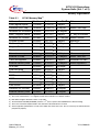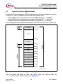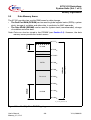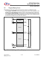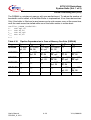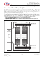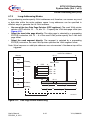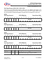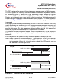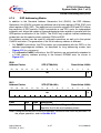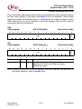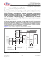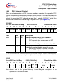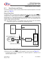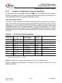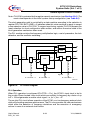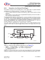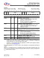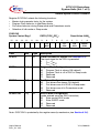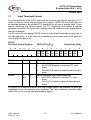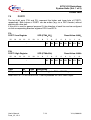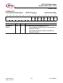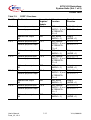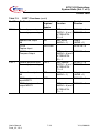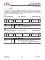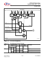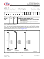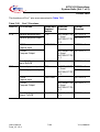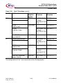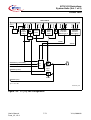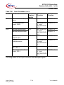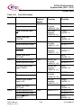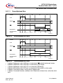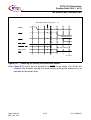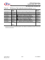
1
U s e r’ s M a n ua l , V 1 . 0 , F e b . 20 0 4
XC161-32
1 6 - B i t S i n g l e - C h i p M i c r o c o n t r o l l er
w i t h C 1 6 6 S V 2 C or e
Volume 1 (of 2): System Units
M i c r o c o n t r o l l er s
N e v e r
s t o p
t h i n k i n g .
Edition 2004-02
Published by Infineon Technologies AG,
St.-Martin-Strasse 53,
81669 München, Germany
© Infineon Technologies AG 2004.
All Rights Reserved.
Attention please!
The information herein is given to describe certain components and shall not be considered as a guarantee of
characteristics.
Terms of delivery and rights to technical change reserved.
We hereby disclaim any and all warranties, including but not limited to warranties of non-infringement, regarding
circuits, descriptions and charts stated herein.
Information
For further information on technology, delivery terms and conditions and prices please contact your nearest
Infineon Technologies Office (www.infineon.com).
Warnings
Due to technical requirements components may contain dangerous substances. For information on the types in
question please contact your nearest Infineon Technologies Office.
Infineon Technologies Components may only be used in life-support devices or systems with the express written
approval of Infineon Technologies, if a failure of such components can reasonably be expected to cause the failure
of that life-support device or system, or to affect the safety or effectiveness of that device or system. Life support
devices or systems are intended to be implanted in the human body, or to support and/or maintain and sustain
and/or protect human life. If they fail, it is reasonable to assume that the health of the user or other persons may
be endangered.
U s e r’ s M a n ua l , V 1 . 0 , F e b . 20 0 4
XC161-32
1 6 - B i t S i n g l e - C h i p M i c r o c o n t r o l l er
w i t h C 1 6 6 S V 2 C or e
Volume 1 (of 2): System Units
M i c r o c o n t r o l l er s
N e v e r
s t o p
t h i n k i n g .
XC161
Volume 1 (of 2): System Units
Revision History:
V1.0, 2004-02
Previous Version:
V1.0, 2003-12 (Pre-Release)
Page
Subjects (major changes since version)1)
1) In order to create the current version V1.0 of this manual, the layout of several graphics and text structures
has been adapted to company documentation rules. The contents have not been changed otherwise, except
for the Pre-release note on page 1-2 or obvious typographical errors.
Controller Area Network (CAN): License of Robert Bosch GmbH
We Listen to Your Comments
Any information within this document that you feel is wrong, unclear or missing at all?
Your feedback will help us to continuously improve the quality of this document.
Please send your proposal (including a reference to this document) to:
[email protected]
Template: mc_tmplt_a5.fm / 3 / 2003-09-01
XC161-32 Derivatives
System Units (Vol. 1 of 2)
Table of Contents
Page
This User’s Manual consists of two Volumes, “System Units” and “Peripheral Units”. For
your convenience this table of contents (and also the keyword index) lists both volumes,
so you can immediately find the reference to the desired section in the corresponding
document ([1] or [2]).
1
1.1
1.2
1.3
1.4
Introduction . . . . . . . . . . . . . . . . . . . . . . . . . . . . . . . . . . . . . . . . . . . . 1-1 [1]
Members of the 16-bit Microcontroller Family . . . . . . . . . . . . . . . . . . . 1-3 [1]
Summary of Basic Features . . . . . . . . . . . . . . . . . . . . . . . . . . . . . . . . 1-5 [1]
Abbreviations . . . . . . . . . . . . . . . . . . . . . . . . . . . . . . . . . . . . . . . . . . . . 1-9 [1]
Naming Conventions . . . . . . . . . . . . . . . . . . . . . . . . . . . . . . . . . . . . . 1-10 [1]
2
2.1
2.1.1
2.1.2
2.1.3
2.1.4
2.1.5
2.1.6
2.2
2.3
2.4
2.5
2.6
2.7
Architectural Overview . . . . . . . . . . . . . . . . . . . . . . . . . . . . . . . . . . . 2-1 [1]
Basic CPU Concepts and Optimizations . . . . . . . . . . . . . . . . . . . . . . . 2-2 [1]
High Instruction Bandwidth/Fast Execution . . . . . . . . . . . . . . . . . . . 2-4 [1]
Powerful Execution Units . . . . . . . . . . . . . . . . . . . . . . . . . . . . . . . . . 2-5 [1]
High Performance Branch-, Call-, and Loop-Processing . . . . . . . . . 2-6 [1]
Consistent and Optimized Instruction Formats . . . . . . . . . . . . . . . . 2-7 [1]
Programmable Multiple Priority Interrupt System . . . . . . . . . . . . . . 2-8 [1]
Interfaces to System Resources . . . . . . . . . . . . . . . . . . . . . . . . . . . 2-9 [1]
On-Chip System Resources . . . . . . . . . . . . . . . . . . . . . . . . . . . . . . . 2-10 [1]
On-Chip Peripheral Blocks . . . . . . . . . . . . . . . . . . . . . . . . . . . . . . . . 2-14 [1]
Clock Generation . . . . . . . . . . . . . . . . . . . . . . . . . . . . . . . . . . . . . . . . 2-28 [1]
Power Management Features . . . . . . . . . . . . . . . . . . . . . . . . . . . . . . 2-28 [1]
On-Chip Debug Support (OCDS) . . . . . . . . . . . . . . . . . . . . . . . . . . . 2-30 [1]
Protected Bits . . . . . . . . . . . . . . . . . . . . . . . . . . . . . . . . . . . . . . . . . . 2-31 [1]
3
3.1
3.2
3.3
3.4
3.5
3.6
3.7
3.8
3.9
3.9.1
3.9.2
3.9.3
3.9.4
3.9.5
3.9.6
Memory Organization . . . . . . . . . . . . . . . . . . . . . . . . . . . . . . . . . . . . 3-1 [1]
Address Mapping . . . . . . . . . . . . . . . . . . . . . . . . . . . . . . . . . . . . . . . . 3-2 [1]
Special Function Register Areas . . . . . . . . . . . . . . . . . . . . . . . . . . . . . 3-4 [1]
Data Memory Areas . . . . . . . . . . . . . . . . . . . . . . . . . . . . . . . . . . . . . . . 3-8 [1]
Program Memory Areas . . . . . . . . . . . . . . . . . . . . . . . . . . . . . . . . . . . 3-10 [1]
System Stack . . . . . . . . . . . . . . . . . . . . . . . . . . . . . . . . . . . . . . . . . . . 3-12 [1]
IO Areas . . . . . . . . . . . . . . . . . . . . . . . . . . . . . . . . . . . . . . . . . . . . . . . 3-13 [1]
External Memory Space . . . . . . . . . . . . . . . . . . . . . . . . . . . . . . . . . . 3-14 [1]
Crossing Memory Boundaries . . . . . . . . . . . . . . . . . . . . . . . . . . . . . . 3-15 [1]
The On-Chip Program Flash Module . . . . . . . . . . . . . . . . . . . . . . . . . 3-16 [1]
Flash Operating Modes . . . . . . . . . . . . . . . . . . . . . . . . . . . . . . . . . 3-18 [1]
Command Sequences . . . . . . . . . . . . . . . . . . . . . . . . . . . . . . . . . . 3-19 [1]
Error Correction and Data Integrity . . . . . . . . . . . . . . . . . . . . . . . . 3-25 [1]
Protection and Security Features . . . . . . . . . . . . . . . . . . . . . . . . . 3-27 [1]
Flash Status Information . . . . . . . . . . . . . . . . . . . . . . . . . . . . . . . . 3-32 [1]
Operation Control and Error Handling . . . . . . . . . . . . . . . . . . . . . . 3-35 [1]
User’s Manual
I-1
V1.0, 2004-02
XC161-32 Derivatives
System Units (Vol. 1 of 2)
Table of Contents
Page
3.10
3.10.1
3.10.2
3.10.3
Program Memory Control . . . . . . . . . . . . . . . . . . . . . . . . . . . . . . . . .
Flash Memory Access . . . . . . . . . . . . . . . . . . . . . . . . . . . . . . . . . .
Program SRAM Access . . . . . . . . . . . . . . . . . . . . . . . . . . . . . . . . .
IMB Control Functions . . . . . . . . . . . . . . . . . . . . . . . . . . . . . . . . . .
4
4.1
4.2
4.2.1
4.2.2
4.2.3
4.3
4.3.1
4.3.2
4.3.3
4.3.4
4.4
4.5
4.5.1
4.5.2
4.6
4.7
4.7.1
4.7.2
4.7.3
4.7.4
4.7.5
4.8
4.8.1
4.8.2
4.8.3
4.9
4.9.1
4.9.2
4.9.3
4.9.4
4.9.5
4.9.6
4.9.7
4.9.8
4.9.9
4.9.10
4.10
Central Processing Unit (CPU) . . . . . . . . . . . . . . . . . . . . . . . . . . . . 4-1 [1]
Components of the CPU . . . . . . . . . . . . . . . . . . . . . . . . . . . . . . . . . . . 4-4 [1]
Instruction Fetch and Program Flow Control . . . . . . . . . . . . . . . . . . . . 4-5 [1]
Branch Detection and Branch Prediction Rules . . . . . . . . . . . . . . . . 4-7 [1]
Correctly Predicted Instruction Flow . . . . . . . . . . . . . . . . . . . . . . . . 4-7 [1]
Incorrectly Predicted Instruction Flow . . . . . . . . . . . . . . . . . . . . . . . 4-9 [1]
Instruction Processing Pipeline . . . . . . . . . . . . . . . . . . . . . . . . . . . . . 4-11 [1]
Pipeline Conflicts Using General Purpose Registers . . . . . . . . . . . 4-13 [1]
Pipeline Conflicts Using Indirect Addressing Modes . . . . . . . . . . . 4-15 [1]
Pipeline Conflicts Due to Memory Bandwidth . . . . . . . . . . . . . . . . 4-17 [1]
Pipeline Conflicts Caused by CPU-SFR Updates . . . . . . . . . . . . . 4-20 [1]
CPU Configuration Registers . . . . . . . . . . . . . . . . . . . . . . . . . . . . . . 4-26 [1]
Use of General Purpose Registers . . . . . . . . . . . . . . . . . . . . . . . . . . 4-29 [1]
GPR Addressing Modes . . . . . . . . . . . . . . . . . . . . . . . . . . . . . . . . 4-31 [1]
Context Switching . . . . . . . . . . . . . . . . . . . . . . . . . . . . . . . . . . . . . 4-33 [1]
Code Addressing . . . . . . . . . . . . . . . . . . . . . . . . . . . . . . . . . . . . . . . . 4-37 [1]
Data Addressing . . . . . . . . . . . . . . . . . . . . . . . . . . . . . . . . . . . . . . . . 4-39 [1]
Short Addressing Modes . . . . . . . . . . . . . . . . . . . . . . . . . . . . . . . . 4-39 [1]
Long Addressing Modes . . . . . . . . . . . . . . . . . . . . . . . . . . . . . . . . 4-41 [1]
Indirect Addressing Modes . . . . . . . . . . . . . . . . . . . . . . . . . . . . . . 4-45 [1]
DSP Addressing Modes . . . . . . . . . . . . . . . . . . . . . . . . . . . . . . . . . 4-47 [1]
The System Stack . . . . . . . . . . . . . . . . . . . . . . . . . . . . . . . . . . . . . 4-53 [1]
Standard Data Processing . . . . . . . . . . . . . . . . . . . . . . . . . . . . . . . . . 4-57 [1]
16-bit Adder/Subtracter, Barrel Shifter, and 16-bit Logic Unit . . . . 4-61 [1]
Bit Manipulation Unit . . . . . . . . . . . . . . . . . . . . . . . . . . . . . . . . . . . 4-61 [1]
Multiply and Divide Unit . . . . . . . . . . . . . . . . . . . . . . . . . . . . . . . . 4-63 [1]
DSP Data Processing (MAC Unit) . . . . . . . . . . . . . . . . . . . . . . . . . . . 4-65 [1]
Representation of Numbers and Rounding . . . . . . . . . . . . . . . . . . 4-66 [1]
The 16-bit by 16-bit Signed/Unsigned Multiplier and Scaler . . . . . 4-67 [1]
Concatenation Unit . . . . . . . . . . . . . . . . . . . . . . . . . . . . . . . . . . . . 4-67 [1]
One-bit Scaler . . . . . . . . . . . . . . . . . . . . . . . . . . . . . . . . . . . . . . . . 4-67 [1]
The 40-bit Adder/Subtracter . . . . . . . . . . . . . . . . . . . . . . . . . . . . . 4-67 [1]
The Data Limiter . . . . . . . . . . . . . . . . . . . . . . . . . . . . . . . . . . . . . . 4-68 [1]
The Accumulator Shifter . . . . . . . . . . . . . . . . . . . . . . . . . . . . . . . . 4-68 [1]
The 40-bit Signed Accumulator Register . . . . . . . . . . . . . . . . . . . . 4-69 [1]
The MAC Unit Status Word MSW . . . . . . . . . . . . . . . . . . . . . . . . . 4-70 [1]
The Repeat Counter MRW . . . . . . . . . . . . . . . . . . . . . . . . . . . . . . 4-72 [1]
Constant Registers . . . . . . . . . . . . . . . . . . . . . . . . . . . . . . . . . . . . . . 4-74 [1]
User’s Manual
I-2
3-37 [1]
3-38 [1]
3-40 [1]
3-41 [1]
V1.0, 2004-02
XC161-32 Derivatives
System Units (Vol. 1 of 2)
Table of Contents
Page
5
5.1
5.2
5.3
5.4
5.4.1
5.4.2
5.4.3
5.4.4
5.5
5.6
5.7
5.8
5.9
5.10
5.11
Interrupt and Trap Functions . . . . . . . . . . . . . . . . . . . . . . . . . . . . . . 5-1 [1]
Interrupt System Structure . . . . . . . . . . . . . . . . . . . . . . . . . . . . . . . . . . 5-2 [1]
Interrupt Arbitration and Control . . . . . . . . . . . . . . . . . . . . . . . . . . . . . 5-4 [1]
Interrupt Vector Table . . . . . . . . . . . . . . . . . . . . . . . . . . . . . . . . . . . . 5-10 [1]
Operation of the Peripheral Event Controller Channels . . . . . . . . . . 5-18 [1]
The PEC Source and Destination Pointers . . . . . . . . . . . . . . . . . . 5-22 [1]
PEC Transfer Control . . . . . . . . . . . . . . . . . . . . . . . . . . . . . . . . . . 5-24 [1]
Channel Link Mode for Data Chaining . . . . . . . . . . . . . . . . . . . . . . 5-26 [1]
PEC Interrupt Control . . . . . . . . . . . . . . . . . . . . . . . . . . . . . . . . . . 5-27 [1]
Prioritization of Interrupt and PEC Service Requests . . . . . . . . . . . . 5-29 [1]
Context Switching and Saving Status . . . . . . . . . . . . . . . . . . . . . . . . 5-31 [1]
Interrupt Node Sharing . . . . . . . . . . . . . . . . . . . . . . . . . . . . . . . . . . . 5-34 [1]
External Interrupts . . . . . . . . . . . . . . . . . . . . . . . . . . . . . . . . . . . . . . 5-35 [1]
OCDS Requests . . . . . . . . . . . . . . . . . . . . . . . . . . . . . . . . . . . . . . . . 5-40 [1]
Service Request Latency . . . . . . . . . . . . . . . . . . . . . . . . . . . . . . . . . 5-41 [1]
Trap Functions . . . . . . . . . . . . . . . . . . . . . . . . . . . . . . . . . . . . . . . . . 5-43 [1]
6
6.1
6.1.1
6.1.2
6.1.3
6.1.4
6.1.5
6.1.6
6.1.7
6.2
6.2.1
6.2.2
6.2.3
6.2.4
6.2.5
6.2.6
6.3
6.3.1
6.3.2
6.3.3
6.3.4
6.3.5
6.3.6
6.4
6.5
General System Control Functions . . . . . . . . . . . . . . . . . . . . . . . . . 6-1 [1]
System Reset . . . . . . . . . . . . . . . . . . . . . . . . . . . . . . . . . . . . . . . . . . . 6-2 [1]
Reset Sources and Phases . . . . . . . . . . . . . . . . . . . . . . . . . . . . . . . 6-3 [1]
Status After Reset . . . . . . . . . . . . . . . . . . . . . . . . . . . . . . . . . . . . . . 6-6 [1]
Application-Specific Initialization Routine . . . . . . . . . . . . . . . . . . . 6-11 [1]
System Startup Configuration . . . . . . . . . . . . . . . . . . . . . . . . . . . . 6-14 [1]
Hardware Configuration in External Start Mode . . . . . . . . . . . . . . 6-18 [1]
Default Configuration in Single-Chip Mode . . . . . . . . . . . . . . . . . . 6-23 [1]
Reset Behavior Control . . . . . . . . . . . . . . . . . . . . . . . . . . . . . . . . . 6-24 [1]
Clock Generation . . . . . . . . . . . . . . . . . . . . . . . . . . . . . . . . . . . . . . . . 6-26 [1]
Oscillators . . . . . . . . . . . . . . . . . . . . . . . . . . . . . . . . . . . . . . . . . . . 6-27 [1]
Clock Generation and Frequency Control . . . . . . . . . . . . . . . . . . . 6-30 [1]
Clock Distribution . . . . . . . . . . . . . . . . . . . . . . . . . . . . . . . . . . . . . . 6-37 [1]
Oscillator Watchdog . . . . . . . . . . . . . . . . . . . . . . . . . . . . . . . . . . . . 6-38 [1]
Interrupt Generation . . . . . . . . . . . . . . . . . . . . . . . . . . . . . . . . . . . . 6-38 [1]
Generation of an External Clock Signal . . . . . . . . . . . . . . . . . . . . 6-39 [1]
Central System Control Functions . . . . . . . . . . . . . . . . . . . . . . . . . . . 6-43 [1]
Status Indication . . . . . . . . . . . . . . . . . . . . . . . . . . . . . . . . . . . . . . 6-45 [1]
Reset Source Indication . . . . . . . . . . . . . . . . . . . . . . . . . . . . . . . . 6-46 [1]
Peripheral Shutdown Handshake . . . . . . . . . . . . . . . . . . . . . . . . . 6-47 [1]
Flexible Peripheral Management . . . . . . . . . . . . . . . . . . . . . . . . . . 6-47 [1]
Debug System Control . . . . . . . . . . . . . . . . . . . . . . . . . . . . . . . . . . 6-49 [1]
Register Security Mechanism . . . . . . . . . . . . . . . . . . . . . . . . . . . . 6-51 [1]
Watchdog Timer (WDT) . . . . . . . . . . . . . . . . . . . . . . . . . . . . . . . . . . 6-55 [1]
Identification Control Block . . . . . . . . . . . . . . . . . . . . . . . . . . . . . . . . 6-60 [1]
User’s Manual
I-3
V1.0, 2004-02
XC161-32 Derivatives
System Units (Vol. 1 of 2)
Table of Contents
Page
7
7.1
7.2
7.3
7.4
7.5
7.6
7.7
7.8
7.9
7.10
7.11
7.12
7.13
Parallel Ports . . . . . . . . . . . . . . . . . . . . . . . . . . . . . . . . . . . . . . . . . . . 7-1 [1]
Input Threshold Control . . . . . . . . . . . . . . . . . . . . . . . . . . . . . . . . . . . . 7-2 [1]
Output Driver Control . . . . . . . . . . . . . . . . . . . . . . . . . . . . . . . . . . . . . . 7-3 [1]
Alternate Port Functions . . . . . . . . . . . . . . . . . . . . . . . . . . . . . . . . . . . 7-8 [1]
PORT0 . . . . . . . . . . . . . . . . . . . . . . . . . . . . . . . . . . . . . . . . . . . . . . . . . 7-9 [1]
PORT1 . . . . . . . . . . . . . . . . . . . . . . . . . . . . . . . . . . . . . . . . . . . . . . . . 7-13 [1]
Port 2 . . . . . . . . . . . . . . . . . . . . . . . . . . . . . . . . . . . . . . . . . . . . . . . . . 7-24 [1]
Port 3 . . . . . . . . . . . . . . . . . . . . . . . . . . . . . . . . . . . . . . . . . . . . . . . . . 7-29 [1]
Port 4 . . . . . . . . . . . . . . . . . . . . . . . . . . . . . . . . . . . . . . . . . . . . . . . . . 7-41 [1]
Port 5 . . . . . . . . . . . . . . . . . . . . . . . . . . . . . . . . . . . . . . . . . . . . . . . . . 7-51 [1]
Port 6 . . . . . . . . . . . . . . . . . . . . . . . . . . . . . . . . . . . . . . . . . . . . . . . . . 7-54 [1]
Port 7 . . . . . . . . . . . . . . . . . . . . . . . . . . . . . . . . . . . . . . . . . . . . . . . . . 7-65 [1]
Port 9 . . . . . . . . . . . . . . . . . . . . . . . . . . . . . . . . . . . . . . . . . . . . . . . . . 7-72 [1]
Port 20 . . . . . . . . . . . . . . . . . . . . . . . . . . . . . . . . . . . . . . . . . . . . . . . . 7-82 [1]
8
Dedicated Pins . . . . . . . . . . . . . . . . . . . . . . . . . . . . . . . . . . . . . . . . . 8-1 [1]
9
9.1
9.2
9.2.1
9.2.1.1
9.2.1.2
9.2.2
9.2.2.1
9.2.2.2
9.2.2.3
9.2.2.4
9.2.2.5
9.2.2.6
9.2.3
9.3
9.3.1
9.3.2
9.3.3
9.3.4
9.3.5
9.3.6
9.3.6.1
9.3.6.2
9.3.7
9.3.7.1
9.3.7.2
The External Bus Controller EBC . . . . . . . . . . . . . . . . . . . . . . . . . . 9-1 [1]
External Bus Signals . . . . . . . . . . . . . . . . . . . . . . . . . . . . . . . . . . . . . . 9-3 [1]
Timing Principles . . . . . . . . . . . . . . . . . . . . . . . . . . . . . . . . . . . . . . . . . 9-4 [1]
Basic Bus Cycle Protocols . . . . . . . . . . . . . . . . . . . . . . . . . . . . . . . . 9-4 [1]
Demultiplexed Bus . . . . . . . . . . . . . . . . . . . . . . . . . . . . . . . . . . . . 9-5 [1]
Multiplexed Bus . . . . . . . . . . . . . . . . . . . . . . . . . . . . . . . . . . . . . . 9-6 [1]
Bus Cycle Phases . . . . . . . . . . . . . . . . . . . . . . . . . . . . . . . . . . . . . . 9-7 [1]
A Phase - CS Change Phase . . . . . . . . . . . . . . . . . . . . . . . . . . . 9-7 [1]
B Phase - Address Setup/ALE Phase . . . . . . . . . . . . . . . . . . . . . 9-7 [1]
C Phase - Delay Phase . . . . . . . . . . . . . . . . . . . . . . . . . . . . . . . . 9-7 [1]
D Phase - Write Data Setup/MUX Tristate Phase . . . . . . . . . . . . 9-7 [1]
E Phase - RD/WR Command Phase . . . . . . . . . . . . . . . . . . . . . . 9-7 [1]
F Phase - Address/Write Data Hold Phase . . . . . . . . . . . . . . . . . 9-8 [1]
Bus Cycle Examples: Fastest Access Cycles . . . . . . . . . . . . . . . . . 9-8 [1]
Functional Description . . . . . . . . . . . . . . . . . . . . . . . . . . . . . . . . . . . . 9-10 [1]
Configuration Register Overview . . . . . . . . . . . . . . . . . . . . . . . . . . 9-10 [1]
The EBC Mode Register 0 . . . . . . . . . . . . . . . . . . . . . . . . . . . . . . . 9-12 [1]
The EBC Mode Register 1 . . . . . . . . . . . . . . . . . . . . . . . . . . . . . . . 9-14 [1]
The Timing Configuration Registers TCONCSx . . . . . . . . . . . . . . 9-15 [1]
The Function Configuration Registers FCONCSx . . . . . . . . . . . . . 9-16 [1]
The Address Window Selection Registers ADDRSELx . . . . . . . . . 9-18 [1]
Definition of Address Areas . . . . . . . . . . . . . . . . . . . . . . . . . . . . 9-18 [1]
Address Window Arbitration . . . . . . . . . . . . . . . . . . . . . . . . . . . 9-20 [1]
Ready Controlled Bus Cycles . . . . . . . . . . . . . . . . . . . . . . . . . . . . 9-21 [1]
General . . . . . . . . . . . . . . . . . . . . . . . . . . . . . . . . . . . . . . . . . . . 9-21 [1]
The Synchronous/Asynchronous READY . . . . . . . . . . . . . . . . . 9-22 [1]
User’s Manual
I-4
V1.0, 2004-02
XC161-32 Derivatives
System Units (Vol. 1 of 2)
Table of Contents
Page
9.3.7.3
9.3.8
9.3.9
9.3.9.1
9.3.9.2
9.3.9.3
9.3.9.4
9.3.9.5
9.3.10
9.4
9.5
Combining the READY Function with Predefined Wait States .
Access Control to TwinCAN . . . . . . . . . . . . . . . . . . . . . . . . . . . . .
External Bus Arbitration . . . . . . . . . . . . . . . . . . . . . . . . . . . . . . . . .
Initialization of Arbitration . . . . . . . . . . . . . . . . . . . . . . . . . . . . . .
Arbitration Master Scheme . . . . . . . . . . . . . . . . . . . . . . . . . . . .
Arbitration Slave Scheme . . . . . . . . . . . . . . . . . . . . . . . . . . . . .
Bus Lock Function . . . . . . . . . . . . . . . . . . . . . . . . . . . . . . . . . . .
Direct Master Slave Connection . . . . . . . . . . . . . . . . . . . . . . . .
Shutdown Control . . . . . . . . . . . . . . . . . . . . . . . . . . . . . . . . . . . . .
LXBus Access Control and Signal Generation . . . . . . . . . . . . . . . . .
EBC Register Table . . . . . . . . . . . . . . . . . . . . . . . . . . . . . . . . . . . . . .
9-22 [1]
9-23 [1]
9-24 [1]
9-24 [1]
9-24 [1]
9-26 [1]
9-27 [1]
9-27 [1]
9-28 [1]
9-29 [1]
9-29 [1]
10
10.1
10.2
10.3
10.4
The Bootstrap Loader . . . . . . . . . . . . . . . . . . . . . . . . . . . . . . . . . .
Entering the Bootstrap Loader . . . . . . . . . . . . . . . . . . . . . . . . . . . . . .
Loading the Startup Code . . . . . . . . . . . . . . . . . . . . . . . . . . . . . . . . .
Exiting Bootstrap Loader Mode . . . . . . . . . . . . . . . . . . . . . . . . . . . . .
Choosing the Baudrate for the BSL . . . . . . . . . . . . . . . . . . . . . . . . .
10-1 [1]
10-2 [1]
10-4 [1]
10-4 [1]
10-5 [1]
11
11.1
11.2
11.3
11.3.1
11.3.2
11.4
11.4.1
Debug System . . . . . . . . . . . . . . . . . . . . . . . . . . . . . . . . . . . . . . . . .
Introduction . . . . . . . . . . . . . . . . . . . . . . . . . . . . . . . . . . . . . . . . . . . .
Debug Interface . . . . . . . . . . . . . . . . . . . . . . . . . . . . . . . . . . . . . . . . .
OCDS Module . . . . . . . . . . . . . . . . . . . . . . . . . . . . . . . . . . . . . . . . . .
Debug Events . . . . . . . . . . . . . . . . . . . . . . . . . . . . . . . . . . . . . . . .
Debug Actions . . . . . . . . . . . . . . . . . . . . . . . . . . . . . . . . . . . . . . . .
Cerberus . . . . . . . . . . . . . . . . . . . . . . . . . . . . . . . . . . . . . . . . . . . . . .
Functional Overview . . . . . . . . . . . . . . . . . . . . . . . . . . . . . . . . . . .
11-1 [1]
11-1 [1]
11-2 [1]
11-3 [1]
11-5 [1]
11-6 [1]
11-7 [1]
11-7 [1]
12
Instruction Set Summary . . . . . . . . . . . . . . . . . . . . . . . . . . . . . . . . 12-1 [1]
13
Device Specification . . . . . . . . . . . . . . . . . . . . . . . . . . . . . . . . . . . . 13-1 [1]
14
14.1
14.1.1
14.1.2
14.1.3
14.1.4
14.1.5
14.1.6
14.1.7
14.2
14.2.1
14.2.2
14.2.3
The General Purpose Timer Units . . . . . . . . . . . . . . . . . . . . . . . . . 14-1 [2]
Timer Block GPT1 . . . . . . . . . . . . . . . . . . . . . . . . . . . . . . . . . . . . . . 14-2 [2]
GPT1 Core Timer T3 Control . . . . . . . . . . . . . . . . . . . . . . . . . . . . 14-4 [2]
GPT1 Core Timer T3 Operating Modes . . . . . . . . . . . . . . . . . . . . . 14-8 [2]
GPT1 Auxiliary Timers T2/T4 Control . . . . . . . . . . . . . . . . . . . . . 14-15 [2]
GPT1 Auxiliary Timers T2/T4 Operating Modes . . . . . . . . . . . . . 14-18 [2]
GPT1 Clock Signal Control . . . . . . . . . . . . . . . . . . . . . . . . . . . . . 14-27 [2]
GPT1 Timer Registers . . . . . . . . . . . . . . . . . . . . . . . . . . . . . . . . . 14-29 [2]
Interrupt Control for GPT1 Timers . . . . . . . . . . . . . . . . . . . . . . . . 14-30 [2]
Timer Block GPT2 . . . . . . . . . . . . . . . . . . . . . . . . . . . . . . . . . . . . . 14-31 [2]
GPT2 Core Timer T6 Control . . . . . . . . . . . . . . . . . . . . . . . . . . . 14-33 [2]
GPT2 Core Timer T6 Operating Modes . . . . . . . . . . . . . . . . . . . . 14-36 [2]
GPT2 Auxiliary Timer T5 Control . . . . . . . . . . . . . . . . . . . . . . . . 14-39 [2]
User’s Manual
I-5
V1.0, 2004-02
XC161-32 Derivatives
System Units (Vol. 1 of 2)
Table of Contents
Page
14.2.4
14.2.5
14.2.6
14.2.7
14.2.8
14.3
GPT2 Auxiliary Timer T5 Operating Modes . . . . . . . . . . . . . . . . .
GPT2 Register CAPREL Operating Modes . . . . . . . . . . . . . . . . .
GPT2 Clock Signal Control . . . . . . . . . . . . . . . . . . . . . . . . . . . . .
GPT2 Timer Registers . . . . . . . . . . . . . . . . . . . . . . . . . . . . . . . . .
Interrupt Control for GPT2 Timers and CAPREL . . . . . . . . . . . . .
Interfaces of the GPT Module . . . . . . . . . . . . . . . . . . . . . . . . . . . . .
15
15.1
15.2
15.3
15.3.1
15.3.2
15.3.3
15.4
Real Time Clock . . . . . . . . . . . . . . . . . . . . . . . . . . . . . . . . . . . . . . . 15-1 [2]
Defining the RTC Time Base . . . . . . . . . . . . . . . . . . . . . . . . . . . . . . . 15-2 [2]
RTC Run Control . . . . . . . . . . . . . . . . . . . . . . . . . . . . . . . . . . . . . . . . 15-5 [2]
RTC Operating Modes . . . . . . . . . . . . . . . . . . . . . . . . . . . . . . . . . . . . 15-7 [2]
48-bit Timer Operation . . . . . . . . . . . . . . . . . . . . . . . . . . . . . . . . . 15-10 [2]
System Clock Operation . . . . . . . . . . . . . . . . . . . . . . . . . . . . . . . 15-10 [2]
Cyclic Interrupt Generation . . . . . . . . . . . . . . . . . . . . . . . . . . . . . 15-11 [2]
RTC Interrupt Generation . . . . . . . . . . . . . . . . . . . . . . . . . . . . . . . . 15-12 [2]
16
16.1
16.1.1
16.1.2
16.2
16.2.1
16.2.2
16.2.3
16.2.4
16.3
16.4
16.5
16.6
The Analog/Digital Converter . . . . . . . . . . . . . . . . . . . . . . . . . . . . 16-1 [2]
Mode Selection . . . . . . . . . . . . . . . . . . . . . . . . . . . . . . . . . . . . . . . . . 16-3 [2]
Compatibility Mode . . . . . . . . . . . . . . . . . . . . . . . . . . . . . . . . . . . . 16-3 [2]
Enhanced Mode . . . . . . . . . . . . . . . . . . . . . . . . . . . . . . . . . . . . . . . 16-5 [2]
ADC Operation . . . . . . . . . . . . . . . . . . . . . . . . . . . . . . . . . . . . . . . . . 16-8 [2]
Fixed Channel Conversion Modes . . . . . . . . . . . . . . . . . . . . . . . . 16-11 [2]
Auto Scan Conversion Modes . . . . . . . . . . . . . . . . . . . . . . . . . . . 16-12 [2]
Wait for Read Mode . . . . . . . . . . . . . . . . . . . . . . . . . . . . . . . . . . . 16-13 [2]
Channel Injection Mode . . . . . . . . . . . . . . . . . . . . . . . . . . . . . . . . 16-14 [2]
Automatic Calibration . . . . . . . . . . . . . . . . . . . . . . . . . . . . . . . . . . . 16-17 [2]
Conversion Timing Control . . . . . . . . . . . . . . . . . . . . . . . . . . . . . . . 16-18 [2]
A/D Converter Interrupt Control . . . . . . . . . . . . . . . . . . . . . . . . . . . . 16-21 [2]
Interfaces of the ADC Module . . . . . . . . . . . . . . . . . . . . . . . . . . . . . 16-22 [2]
17
17.1
17.2
17.3
17.4
17.5
17.5.1
17.5.2
17.5.3
17.5.4
17.5.5
17.6
17.7
17.8
Capture/Compare Units . . . . . . . . . . . . . . . . . . . . . . . . . . . . . . . . . . 17-1 [2]
The CAPCOM Timers . . . . . . . . . . . . . . . . . . . . . . . . . . . . . . . . . . . . 17-4 [2]
CAPCOM Timer Interrupts . . . . . . . . . . . . . . . . . . . . . . . . . . . . . . . . . 17-9 [2]
Capture/Compare Channels . . . . . . . . . . . . . . . . . . . . . . . . . . . . . . 17-10 [2]
Capture Mode Operation . . . . . . . . . . . . . . . . . . . . . . . . . . . . . . . . . 17-13 [2]
Compare Mode Operation . . . . . . . . . . . . . . . . . . . . . . . . . . . . . . . . 17-14 [2]
Compare Mode 0 . . . . . . . . . . . . . . . . . . . . . . . . . . . . . . . . . . . . . 17-15 [2]
Compare Mode 1 . . . . . . . . . . . . . . . . . . . . . . . . . . . . . . . . . . . . . 17-15 [2]
Compare Mode 2 . . . . . . . . . . . . . . . . . . . . . . . . . . . . . . . . . . . . . 17-18 [2]
Compare Mode 3 . . . . . . . . . . . . . . . . . . . . . . . . . . . . . . . . . . . . . 17-18 [2]
Double-Register Compare Mode . . . . . . . . . . . . . . . . . . . . . . . . 17-22 [2]
Compare Output Signal Generation . . . . . . . . . . . . . . . . . . . . . . . . 17-25 [2]
Single Event Operation . . . . . . . . . . . . . . . . . . . . . . . . . . . . . . . . . . 17-27 [2]
Staggered and Non-Staggered Operation . . . . . . . . . . . . . . . . . . . . 17-29 [2]
User’s Manual
I-6
14-41 [2]
14-45 [2]
14-50 [2]
14-53 [2]
14-54 [2]
14-55 [2]
V1.0, 2004-02
XC161-32 Derivatives
System Units (Vol. 1 of 2)
Table of Contents
Page
17.9
17.10
17.11
CAPCOM Interrupts . . . . . . . . . . . . . . . . . . . . . . . . . . . . . . . . . . . . . 17-34 [2]
External Input Signal Requirements . . . . . . . . . . . . . . . . . . . . . . . . 17-36 [2]
Interfaces of the CAPCOM Units . . . . . . . . . . . . . . . . . . . . . . . . . . . 17-37 [2]
18
18.1
18.2
18.2.1
18.2.2
18.2.3
18.2.4
18.2.5
18.2.6
18.2.7
18.2.8
18.3
18.3.1
18.3.2
18.3.3
18.4
18.4.1
18.4.2
18.5
18.5.1
18.5.2
18.5.3
18.5.4
18.6
18.7
18.8
18.9
Asynchronous/Synchronous Serial Interface (ASC) . . . . . . . . . . 18-1 [2]
Operational Overview . . . . . . . . . . . . . . . . . . . . . . . . . . . . . . . . . . . . 18-3 [2]
Asynchronous Operation . . . . . . . . . . . . . . . . . . . . . . . . . . . . . . . . . 18-5 [2]
Asynchronous Data Frames . . . . . . . . . . . . . . . . . . . . . . . . . . . . . 18-6 [2]
Asynchronous Transmission . . . . . . . . . . . . . . . . . . . . . . . . . . . . . 18-9 [2]
Transmit FIFO Operation . . . . . . . . . . . . . . . . . . . . . . . . . . . . . . . 18-9 [2]
Asynchronous Reception . . . . . . . . . . . . . . . . . . . . . . . . . . . . . . . 18-12 [2]
Receive FIFO Operation . . . . . . . . . . . . . . . . . . . . . . . . . . . . . . . 18-12 [2]
FIFO Transparent Mode . . . . . . . . . . . . . . . . . . . . . . . . . . . . . . . 18-15 [2]
IrDA Mode . . . . . . . . . . . . . . . . . . . . . . . . . . . . . . . . . . . . . . . . . . 18-16 [2]
RxD/TxD Data Path Selection in Asynchronous Modes . . . . . . . 18-17 [2]
Synchronous Operation . . . . . . . . . . . . . . . . . . . . . . . . . . . . . . . . . 18-19 [2]
Synchronous Transmission . . . . . . . . . . . . . . . . . . . . . . . . . . . . . 18-20 [2]
Synchronous Reception . . . . . . . . . . . . . . . . . . . . . . . . . . . . . . . . 18-20 [2]
Synchronous Timing . . . . . . . . . . . . . . . . . . . . . . . . . . . . . . . . . . 18-20 [2]
Baudrate Generation . . . . . . . . . . . . . . . . . . . . . . . . . . . . . . . . . . . 18-22 [2]
Baudrate in Asynchronous Mode . . . . . . . . . . . . . . . . . . . . . . . . . 18-22 [2]
Baudrate in Synchronous Mode . . . . . . . . . . . . . . . . . . . . . . . . . 18-26 [2]
Autobaud Detection . . . . . . . . . . . . . . . . . . . . . . . . . . . . . . . . . . . . 18-27 [2]
General Operation . . . . . . . . . . . . . . . . . . . . . . . . . . . . . . . . . . . . 18-27 [2]
Serial Frames for Autobaud Detection . . . . . . . . . . . . . . . . . . . . . 18-28 [2]
Baudrate Selection and Calculation . . . . . . . . . . . . . . . . . . . . . . . 18-29 [2]
Overwriting Registers on Successful Autobaud Detection . . . . . 18-33 [2]
Hardware Error Detection Capabilities . . . . . . . . . . . . . . . . . . . . . . 18-34 [2]
Interrupts . . . . . . . . . . . . . . . . . . . . . . . . . . . . . . . . . . . . . . . . . . . . . 18-35 [2]
Registers . . . . . . . . . . . . . . . . . . . . . . . . . . . . . . . . . . . . . . . . . . . . . 18-39 [2]
Interfaces of the ASC Modules . . . . . . . . . . . . . . . . . . . . . . . . . . . . 18-56 [2]
19
19.1
19.2
19.2.1
19.2.2
19.2.3
19.2.4
19.2.5
19.2.6
19.2.7
19.2.8
High-Speed Synchronous Serial Interface (SSC) . . . . . . . . . . . . 19-1 [2]
Introduction . . . . . . . . . . . . . . . . . . . . . . . . . . . . . . . . . . . . . . . . . . . . 19-1 [2]
Operational Overview . . . . . . . . . . . . . . . . . . . . . . . . . . . . . . . . . . . . 19-1 [2]
Operating Mode Selection . . . . . . . . . . . . . . . . . . . . . . . . . . . . . . . 19-3 [2]
Full-Duplex Operation . . . . . . . . . . . . . . . . . . . . . . . . . . . . . . . . . . 19-8 [2]
Half-Duplex Operation . . . . . . . . . . . . . . . . . . . . . . . . . . . . . . . . 19-11 [2]
Continuous Transfers . . . . . . . . . . . . . . . . . . . . . . . . . . . . . . . . . 19-12 [2]
Baudrate Generation . . . . . . . . . . . . . . . . . . . . . . . . . . . . . . . . . 19-12 [2]
Error Detection Mechanisms . . . . . . . . . . . . . . . . . . . . . . . . . . . 19-14 [2]
SSC Register Summary . . . . . . . . . . . . . . . . . . . . . . . . . . . . . . . . 19-16 [2]
Port Configuration Requirements . . . . . . . . . . . . . . . . . . . . . . . . 19-17 [2]
User’s Manual
I-7
V1.0, 2004-02
XC161-32 Derivatives
System Units (Vol. 1 of 2)
Table of Contents
Page
19.3
Interfaces of the SSC Modules . . . . . . . . . . . . . . . . . . . . . . . . . . . . 19-18 [2]
20
20.1
20.2
20.3
20.3.1
20.3.2
20.3.3
20.3.4
20.3.5
20.3.6
20.4
20.5
20.6
20.7
IIC-Bus Module . . . . . . . . . . . . . . . . . . . . . . . . . . . . . . . . . . . . . . . . 20-1 [2]
Overview . . . . . . . . . . . . . . . . . . . . . . . . . . . . . . . . . . . . . . . . . . . . . . 20-2 [2]
Register Description . . . . . . . . . . . . . . . . . . . . . . . . . . . . . . . . . . . . . 20-5 [2]
IIC-Bus Module Operation . . . . . . . . . . . . . . . . . . . . . . . . . . . . . . . 20-12 [2]
Operation in Single-Master Mode . . . . . . . . . . . . . . . . . . . . . . . . 20-12 [2]
Operation in Multimaster Mode . . . . . . . . . . . . . . . . . . . . . . . . . . 20-12 [2]
Operation in Slave Mode . . . . . . . . . . . . . . . . . . . . . . . . . . . . . . 20-13 [2]
Transmit/Receive Buffer . . . . . . . . . . . . . . . . . . . . . . . . . . . . . . . 20-14 [2]
Baud Rate Generation . . . . . . . . . . . . . . . . . . . . . . . . . . . . . . . . . 20-15 [2]
Notes for Programming the IIC-Bus Module . . . . . . . . . . . . . . . . 20-16 [2]
Interrupt Request Operation . . . . . . . . . . . . . . . . . . . . . . . . . . . . . . 20-17 [2]
Port Connection and Configuration . . . . . . . . . . . . . . . . . . . . . . . . . 20-19 [2]
Interfaces of the IIC-Bus Module . . . . . . . . . . . . . . . . . . . . . . . . . . . 20-21 [2]
IIC-Bus Overview . . . . . . . . . . . . . . . . . . . . . . . . . . . . . . . . . . . . . . . 20-22 [2]
21
TwinCAN Module . . . . . . . . . . . . . . . . . . . . . . . . . . . . . . . . . . . . . . 21-1 [2]
21.1
Kernel Description . . . . . . . . . . . . . . . . . . . . . . . . . . . . . . . . . . . . . . . 21-1 [2]
21.1.1
Overview . . . . . . . . . . . . . . . . . . . . . . . . . . . . . . . . . . . . . . . . . . . . 21-1 [2]
21.1.2
TwinCAN Control Shell . . . . . . . . . . . . . . . . . . . . . . . . . . . . . . . . . 21-4 [2]
21.1.2.1
Initialization Processing . . . . . . . . . . . . . . . . . . . . . . . . . . . . . . 21-4 [2]
21.1.2.2
Interrupt Request Compressor . . . . . . . . . . . . . . . . . . . . . . . . . 21-5 [2]
21.1.2.3
Global Control and Status Logic . . . . . . . . . . . . . . . . . . . . . . . . 21-6 [2]
21.1.3
CAN Node Control Logic . . . . . . . . . . . . . . . . . . . . . . . . . . . . . . . 21-7 [2]
21.1.3.1
Overview . . . . . . . . . . . . . . . . . . . . . . . . . . . . . . . . . . . . . . . . . . 21-7 [2]
21.1.3.2
Timing Control Unit . . . . . . . . . . . . . . . . . . . . . . . . . . . . . . . . . . 21-9 [2]
21.1.3.3
Bitstream Processor . . . . . . . . . . . . . . . . . . . . . . . . . . . . . . . . 21-11 [2]
21.1.3.4
Error Handling Logic . . . . . . . . . . . . . . . . . . . . . . . . . . . . . . . . 21-11 [2]
21.1.3.5
Node Interrupt Processing . . . . . . . . . . . . . . . . . . . . . . . . . . . 21-12 [2]
21.1.3.6
Message Interrupt Processing . . . . . . . . . . . . . . . . . . . . . . . . 21-13 [2]
21.1.3.7
Interrupt Indication . . . . . . . . . . . . . . . . . . . . . . . . . . . . . . . . . 21-13 [2]
21.1.4
Message Handling Unit . . . . . . . . . . . . . . . . . . . . . . . . . . . . . . . . 21-15 [2]
21.1.4.1
Arbitration and Acceptance Mask Register . . . . . . . . . . . . . . . 21-16 [2]
21.1.4.2
Handling of Remote and Data Frames . . . . . . . . . . . . . . . . . . 21-17 [2]
21.1.4.3
Handling of Transmit Message Objects . . . . . . . . . . . . . . . . . . 21-18 [2]
21.1.4.4
Handling of Receive Message Objects . . . . . . . . . . . . . . . . . . 21-21 [2]
21.1.4.5
Single Data Transfer Mode . . . . . . . . . . . . . . . . . . . . . . . . . . . 21-23 [2]
21.1.5
CAN Message Object Buffer (FIFO) . . . . . . . . . . . . . . . . . . . . . . 21-24 [2]
21.1.5.1
Buffer Access by the CAN Controller . . . . . . . . . . . . . . . . . . . 21-26 [2]
21.1.5.2
Buffer Access by the CPU . . . . . . . . . . . . . . . . . . . . . . . . . . . . 21-27 [2]
21.1.6
Gateway Message Handling . . . . . . . . . . . . . . . . . . . . . . . . . . . . 21-28 [2]
21.1.6.1
Normal Gateway Mode . . . . . . . . . . . . . . . . . . . . . . . . . . . . . . 21-29 [2]
User’s Manual
I-8
V1.0, 2004-02
XC161-32 Derivatives
System Units (Vol. 1 of 2)
Table of Contents
Page
21.1.6.2
Normal Gateway with FIFO Buffering . . . . . . . . . . . . . . . . . . .
21.1.6.3
Shared Gateway Mode . . . . . . . . . . . . . . . . . . . . . . . . . . . . . .
21.1.7
Programming the TwinCAN Module . . . . . . . . . . . . . . . . . . . . . .
21.1.7.1
Configuration of CAN Node A/B . . . . . . . . . . . . . . . . . . . . . . .
21.1.7.2
Initialization of Message Objects . . . . . . . . . . . . . . . . . . . . . . .
21.1.7.3
Controlling a Message Transfer . . . . . . . . . . . . . . . . . . . . . . .
21.1.8
Loop-Back Mode . . . . . . . . . . . . . . . . . . . . . . . . . . . . . . . . . . . . .
21.1.9
Single Transmission Try Functionality . . . . . . . . . . . . . . . . . . . .
21.1.10
Module Clock Requirements . . . . . . . . . . . . . . . . . . . . . . . . . . . .
21.2
TwinCAN Register Description . . . . . . . . . . . . . . . . . . . . . . . . . . . .
21.2.1
Register Map . . . . . . . . . . . . . . . . . . . . . . . . . . . . . . . . . . . . . . .
21.2.2
CAN Node A/B Registers . . . . . . . . . . . . . . . . . . . . . . . . . . . . . . .
21.2.3
CAN Message Object Registers . . . . . . . . . . . . . . . . . . . . . . . . .
21.2.4
Global CAN Control/Status Registers . . . . . . . . . . . . . . . . . . . . .
21.3
XC161 Module Implementation Details . . . . . . . . . . . . . . . . . . . . . .
21.3.1
Interfaces of the TwinCAN Module . . . . . . . . . . . . . . . . . . . . . . .
21.3.2
TwinCAN Module Related External Registers . . . . . . . . . . . . . . .
21.3.2.1
System Registers . . . . . . . . . . . . . . . . . . . . . . . . . . . . . . . . . . .
21.3.2.2
Port Registers . . . . . . . . . . . . . . . . . . . . . . . . . . . . . . . . . . . . .
21.3.2.3
Interrupt Registers . . . . . . . . . . . . . . . . . . . . . . . . . . . . . . . . . .
21.3.3
Register Table . . . . . . . . . . . . . . . . . . . . . . . . . . . . . . . . . . . . . . .
22
22.1
22.2
21-33 [2]
21-36 [2]
21-40 [2]
21-40 [2]
21-40 [2]
21-41 [2]
21-44 [2]
21-45 [2]
21-46 [2]
21-47 [2]
21-47 [2]
21-49 [2]
21-64 [2]
21-80 [2]
21-82 [2]
21-82 [2]
21-83 [2]
21-84 [2]
21-85 [2]
21-90 [2]
21-91 [2]
Register Set . . . . . . . . . . . . . . . . . . . . . . . . . . . . . . . . . . . . . . . . . . . 22-1 [2]
PD+BUS Peripherals . . . . . . . . . . . . . . . . . . . . . . . . . . . . . . . . . . . . . 22-1 [2]
LXBUS Peripherals . . . . . . . . . . . . . . . . . . . . . . . . . . . . . . . . . . . . . 22-14 [2]
Keyword Index . . . . . . . . . . . . . . . . . . . . . . . . . . . . . . . . . . . . . . . . . i-1 [1+2]
User’s Manual
I-9
V1.0, 2004-02
XC161-32 Derivatives
System Units (Vol. 1 of 2)
Introduction
1
Introduction
The rapidly growing area of embedded control applications is representing one of the
most time-critical operating environments for today’s microcontrollers. Complex control
algorithms have to be processed based on a large number of digital as well as analog
input signals, and the appropriate output signals must be generated within a defined
maximum response time. Embedded control applications also are often sensitive to
board space, power consumption, and overall system cost.
Embedded control applications therefore require microcontrollers, which:
•
•
•
•
offer a high level of system integration
eliminate the need for additional peripheral devices and the associated software
overhead
provide system security and fail-safe mechanisms
provide effective means to control (and reduce) the device’s power consumption
The increasing complexity of embedded control applications requires microcontrollers
for new high-end embedded control systems to possess a significant increase in CPU
performance and peripheral functionality over conventional 8-bit controllers. To achieve
this high performance goal Infineon has decided to develop its families of 16-bit CMOS
microcontrollers without the constraints of backward compatibility.
Nonetheless the architectures of the 16-bit microcontroller families pursue successful
hardware and software concepts, which have been established in Infineon’s popular
8-bit controller families.
User’s Manual
Introduction_X1, V2.2
1-1
V1.0, 2004-02
XC161-32 Derivatives
System Units (Vol. 1 of 2)
Introduction
About this Manual
This manual describes the functionality of a number of 16-bit microcontrollers of the
Infineon XC166 Family.
These microcontrollers provide identical functionality to a large extent, but each device
type has specific unique features as indicated here.
The descriptions in this manual cover a superset of the provided features and refer to the
following derivatives:
•
XC161CS-32F
– 256 Kbytes Program Flash, 12 Kbytes on-chip RAM,
– 12 analog input channels,
– 7 serial interfaces (2 × ASC, 2 × SSC, 2 × CAN, IIC)
This manual is valid for these derivatives and describes all variations of the different
available temperature ranges and packages.
For simplicity, these various device types are referred to by the collective term XC161
throughout this manual. The complete pro-electron conforming designations are listed in
the respective data sheets.
Some sections of this manual do not refer to all of the XC161 derivatives which are
currently available or planned (such as devices with different types of on-chip memory
or peripherals). These sections contain respective notes wherever possible.
User’s Manual
Introduction_X1, V2.2
1-2
V1.0, 2004-02
XC161-32 Derivatives
System Units (Vol. 1 of 2)
Introduction
1.1
Members of the 16-bit Microcontroller Family
The microcontrollers in the Infineon 16-bit family have been designed to meet the high
performance requirements of real-time embedded control applications. The architecture
of this family has been optimized for high instruction throughput and minimized response
time to external stimuli (interrupts). Intelligent peripheral subsystems have been
integrated to reduce the need for CPU intervention to a minimum extent. This also
minimizes the need for communication via the external bus interface. The high flexibility
of this architecture allows to serve the diverse and varying needs of different application
areas such as automotive, industrial control, or data communications.
The core of the 16-bit family has been developed with a modular family concept in mind.
All family members execute an efficient control-optimized instruction set (additional
instructions for members of the second generation). This allows easy and quick
implementation of new family members with different internal memory sizes and
technologies, different sets of on-chip peripherals, and/or different numbers of IO pins.
The XBUS concept (internal representation of the external bus interface) provides a
straightforward path for building application-specific derivatives by integrating
application-specific peripheral modules with the standard on-chip peripherals.
As programs for embedded control applications become larger, high level languages are
favored by programmers, because high level language programs are easier to write, to
debug and to maintain. The C166 Family supports this starting with its 2nd generation.
The 80C166-type microcontrollers were the first generation of the 16-bit controller
family. These devices established the C166 architecture.
The C165-type and C167-type devices are members of the second generation of this
family. This second generation is even more powerful due to additional instructions for
HLL support, an increased address space, increased internal RAM, and highly efficient
management of various resources on the external bus.
Enhanced derivatives of this second generation provide more features such as
additional internal high-speed RAM, an integrated CAN-Module, an on-chip PLL, etc.
The design of more efficient systems may require the integration of application-specific
peripherals to boost system performance while minimizing the part count. These efforts
are supported by the XBUS, defined for the Infineon 16-bit microcontrollers (second
generation). The XBUS is an internal representation of the external bus interface which
opens and simplifies the integration of peripherals by standardizing the required
interface. One representative taking advantage of this technology is the integrated CAN
module.
The C165-type devices are reduced functionality versions of the C167 because they do
not have the A/D converter, the CAPCOM units, and the PWM module. This results in a
smaller package, reduced power consumption, and design savings.
User’s Manual
Introduction_X1, V2.2
1-3
V1.0, 2004-02
XC161-32 Derivatives
System Units (Vol. 1 of 2)
Introduction
The C164-type devices, the C167CS derivatives, and some of the C161-type devices
are further enhanced by a flexible power management and form the third generation of
the 16-bit controller family. This power management mechanism provides an effective
means to control the power that is consumed in a certain state of the controller and thus
minimizes the overall power consumption for a given application.
The XC16x derivatives represent the fourth generation of the 16-bit controller family.
The XC166 Family dramatically increases the performance of 16-bit microcontrollers by
several major improvements and additions. The MAC-unit adds DSP-functionality to
handle digital filter algorithms and greatly reduces the execution time of multiplications
and divisions. The 5-stage pipeline, single-cycle execution of most instructions, and
PEC-transfers within the complete addressing range increase system performance.
Debugging the target system is supported by integrated functions for On-Chip Debug
Support (OCDS).
A variety of different versions is provided which offer various kinds of on-chip program
memory1):
•
•
•
•
Mask-programmable ROM
Flash memory
OTP memory
ROMless without non-volatile memory.
Also there are devices with specific functional units.
The devices may be offered in different packages, temperature ranges and speed
classes.
Additional standard and application-specific derivatives are planned and are in
development.
Note: Not all derivatives will be offered in all temperature ranges, speed classes,
packages, or program memory variations.
Information about specific versions and derivatives will be made available with the
devices themselves. Contact your Infineon representative for up-to-date material or refer
to http://www.infineon.com/microcontrollers.
Note: As the architecture and the basic features, such as the CPU core and built-in
peripherals, are identical for most of the currently offered versions of the XC161,
descriptions within this manual that refer to the “XC161” also apply to the other
variations, unless otherwise noted.
1) Not all derivatives are offered with all kinds of on-chip memory.
User’s Manual
Introduction_X1, V2.2
1-4
V1.0, 2004-02
XC161-32 Derivatives
System Units (Vol. 1 of 2)
Introduction
1.2
Summary of Basic Features
The XC161 devices are enhanced members of the Infineon family of full featured 16-bit
single-chip CMOS microcontrollers. The XC161 combines the extended functionality
and performance of the C166SV2 Core with powerful on-chip peripheral subsystems
and on-chip memory units and provides a means for power reduction.
Several key features contribute to the high performance of the XC161:
High Performance 16-bit CPU with Five-Stage Pipeline and MAC Unit
•
•
•
•
•
•
•
•
•
•
•
•
•
•
Single clock cycle instruction execution
1 cycle minimum instruction cycle time (most instructions)
1 cycle multiplication (16-bit × 16-bit)
4 + 17 cycles division (32-bit/16-bit), 4 cycles delay, 17 cycles background execution
1 cycle multiply and accumulate instruction (MAC) execution
Automatic saturation or rounding included
Multiple high bandwidth internal data buses
Register-based design with multiple, variable register banks
Two additional fast register banks
Fast context switching support
16 Mbytes of linear address space for code and data (Von Neumann architecture)
System stack cache support with automatic stack overflow/underflow detection
High performance branch, call, and loop processing
Zero-cycle jump execution
Control Oriented Instruction Set with High Efficiency
•
•
•
•
•
Bit, byte, and word data types
Flexible and efficient addressing modes for high code density
Enhanced boolean bit manipulation with direct addressability of 6 Kbits for peripheral
control and user-defined flags
Hardware traps to identify exception conditions during runtime
HLL support for semaphore operations and efficient data access
Power Management Features
•
•
•
•
•
Gated clock concept for improved power consumption and EMC
Programmable system slowdown via clock generation unit
Flexible management of peripherals, can be individually disabled
Sleep-mode supports wake-up via fast external interrupts or on-chip RTC
Programmable frequency output
User’s Manual
Introduction_X1, V2.2
1-5
V1.0, 2004-02
XC161-32 Derivatives
System Units (Vol. 1 of 2)
Introduction
Integrated On-Chip Memory
•
•
•
•
Up to 2 Kbytes Dual-Port RAM (DPRAM) for variables, register banks, and stacks
Up to 4 Kbytes on-chip high-speed Data SRAM (DSRAM) for variables and stacks
Up to 6 Kbytes on-chip high-speed Program/Data SRAM (PSRAM) for code and data
256 Kbytes on-chip Program Memory for instruction code or constant data
(Flash or Mask ROM, not for ROMless devices)
Note: The system stack can be located in any memory area within the complete
addressing range.
External Bus Interface
•
•
•
•
•
•
Up to 12 Mbytes external address space for code and data
Multiplexed or demultiplexed bus configurations
Segmentation capability and chip select signal generation
8-bit or 16-bit data bus
Bus cycle characteristics selectable for five programmable address areas
Hold- and Hold-Acknowledge bus arbitration support for external multimaster bus
16-Priority-Level Interrupt System
•
•
•
•
•
80 interrupt nodes with separate interrupt vectors on 15 priority levels (8 group levels)
13 cycles minimum interrupt latency in case of internal program execution
Fast external interrupts
Programmable external interrupt source selection
Programmable vector table (start location and step-width)
8-Channel Peripheral Event Controller (PEC)
•
•
•
•
•
•
Interrupt driven single cycle data transfer
Programmable PEC interrupt request level, (15 down to 8)
Transfer count option
(standard CPU interrupt after programmable number of PEC transfers)
Separate interrupt level for PEC termination interrupts selectable
Overhead from saving and restoring system state for interrupt requests eliminated
Full 24-bit addresses for source and destination pointers, supporting transfers within
the total address space
Intelligent On-Chip Peripheral Subsystems
•
•
12-channel A/D Converter with programmable resolution (10-bit or 8-bit) and
conversion time (down to 2.55 µs or 2.15 µs), auto scan modes, channel injection
Two Capture/Compare Units with 2 independent time bases each,
very flexible PWM unit/event recording unit with different operating modes,
includes four 16-bit timers/counters, maximum resolution fSYS
User’s Manual
Introduction_X1, V2.2
1-6
V1.0, 2004-02
XC161-32 Derivatives
System Units (Vol. 1 of 2)
Introduction
•
•
•
•
•
•
•
•
Two Multifunctional General Purpose Timer Units:
– GPT1: three 16-bit timers/counters, maximum resolution fSYS/4
– GPT2: two 16-bit timers/counters, maximum resolution fSYS/2
Two Asynchronous/Synchronous Serial Channels (USARTs)
with baud rate generator, parity, framing, and overrun error detection,
with auto baud rate detection, receive/transmit FIFOs, and IrDA support
Two High Speed Synchronous Serial Channels (SPI-compatible)
with programmable data length and shift direction
Controller Area Network (TwinCAN) Module, Rev. 2.0B active, two nodes operating
independently or exchanging data via a gateway function, Full-CAN/Basic-CAN
Real Time Clock with alarm interrupt
Watchdog Timer with programmable time intervals
Bootstrap Loader for flexible system initialization
Protection management for system configuration and control registers
On-Chip Debug Support
•
•
•
•
•
•
•
•
On-chip debug controller and related interface to JTAG controller
JTAG interface and break interface on separate pins
Hardware, software and external pin breakpoints
Up to 4 instruction pointer breakpoints
Debug event control, e.g. with monitor call or CPU halt or trigger of data transfer
Dedicated DEBUG instructions with control via JTAG interface
Access to any internal register or memory location via JTAG interface
Single step support and watchpoints with MOV-injection
Up to 99 IO Lines With Individual Bit Addressability
•
•
•
•
•
Tri-stated in input mode
Selectable input thresholds (not on all pins)
Push/pull or open drain output mode
Programmable port driver control
I/O voltage is 5 V (core-logic and oscillator input voltage is 2.5 V)
Various Temperature Ranges1)
•
•
•
0 to +70 °C
-40 to +85 °C
-40 to +125 °C
1) Not all derivatives are offered in all temperature ranges.
User’s Manual
Introduction_X1, V2.2
1-7
V1.0, 2004-02
XC161-32 Derivatives
System Units (Vol. 1 of 2)
Introduction
Infineon CMOS Process
•
Low power CMOS technology enables power saving Idle, Sleep, and Power Down
modes with flexible power management.
144-Pin Plastic Thin Quad Flat Pack (TQFP) Package
•
P-TQFP, 20 × 20 mm body, 0.5 mm (19.7 mil) lead spacing,
surface mount technology
Complete Development Support
For the development tool support of its microcontrollers, Infineon follows a clear third
party concept. Currently around 120 tool suppliers world-wide, ranging from local niche
manufacturers to multinational companies with broad product portfolios, offer powerful
development tools for the Infineon C500, C166, and XC166 microcontroller families,
guaranteeing a remarkable variety of price-performance classes as well as early
availability of high quality key tools such as compilers, assemblers, simulators,
debuggers or in-circuit emulators.
Infineon incorporates its strategic tool partners very early into the product development
process, making sure embedded system developers get reliable, well-tuned tool
solutions, which help them unleash the power of Infineon microcontrollers in the most
effective way and with the shortest possible learning curve.
The tool environment for the Infineon 16-bit microcontrollers includes the following tools:
•
•
•
•
•
•
•
•
•
•
•
•
•
•
Compilers (C, MODULA2, FORTH)
Macro-assemblers, linkers, locators, library managers, format-converters
Architectural simulators
HLL debuggers
Real-time operating systems
VHDL chip models
In-circuit emulators (based on bondout or standard chips)
Plug-in emulators
Emulation and clip-over adapters, production sockets
Logic analyzer disassemblers
Starter kits
Evaluation boards with monitor programs
Industrial boards (also for CAN, FUZZY, PROFIBUS, FORTH applications)
Network driver software (CAN, PROFIBUS)
User’s Manual
Introduction_X1, V2.2
1-8
V1.0, 2004-02
XC161-32 Derivatives
System Units (Vol. 1 of 2)
Introduction
1.3
Abbreviations
The following acronyms and terms are used within this document:
JTAG
Joint Test Access Group
ADC
Analog Digital Converter
ALE
Address Latch Enable
ALU
Arithmetic and Logic Unit
ASC
Asynchronous/synchronous Serial Channel
CAN
Controller Area Network (License Bosch)
CAPCOM
CAPture and COMpare unit
CISC
Complex Instruction Set Computing
CMOS
Complementary Metal Oxide Silicon
CPU
Central Processing Unit
DMU
Data Management Unit
EBC
External Bus Controller
ESFR
Extended Special Function Register
Flash
Non-volatile memory that may be electrically erased
GPR
General Purpose Register
GPT
General Purpose Timer unit
HLL
High Level Language
IIC
Inter Integrated Circuit (Bus)
IO
Input/Output
LXBus
Internal representation of the external bus
OCDS
On-Chip Debug Support
OTP
One-Time Programmable memory
PEC
Peripheral Event Controller
PLA
Programmable Logic Array
PLL
Phase Locked Loop
PMU
Program Management Unit
PWM
Pulse Width Modulation
RAM
Random Access Memory
RISC
Reduced Instruction Set Computing
User’s Manual
Introduction_X1, V2.2
1-9
V1.0, 2004-02
XC161-32 Derivatives
System Units (Vol. 1 of 2)
Introduction
ROM
Read Only Memory
RTC
Real Time Clock
SFR
Special Function Register
SSC
Synchronous Serial Channel
1.4
Naming Conventions
The manifold bitfields used for control functions and status indication and the registers
housing them are equipped with unique names wherever applicable. Thereby these
control structured can be referred to by their names rather than by their location. This
makes the descriptions by far more comprehensible.
To describe regular structures (such as ports) indices are used instead of a plethora of
similar bit names, so bit 3 of port 5 is referred to as P5.3.
Where it helps to clarify the relation between several named structures, the next higher
level is added to the respective name to make it unambiguous.
The term ADC_CTR0 clearly identifies register CTR0 as part of module ADC, the term
SYSCON1.CPSYS clearly identifies bitfield CPSYS as part of register SYSCON1.
User’s Manual
Introduction_X1, V2.2
1-10
V1.0, 2004-02
XC161-32 Derivatives
System Units (Vol. 1 of 2)
Architectural Overview
2
Architectural Overview
The architecture of the XC161 core combines the advantages of both RISC and CISC
processors in a very well-balanced way. This computing and controlling power is
completed by the DSP-functionality of the MAC-unit. The XC161 integrates this powerful
CPU core with a set of powerful peripheral units into one chip and connects them very
efficiently. On-chip memory blocks with dedicated buses and control units store code
and data. This combination of features results in a high performance microcontroller,
which is the right choice not only for today’s applications, but also for future engineering
challenges. One of the buses used concurrently on the XC161 is the LXBus, an internal
representation of the external bus interface. This bus provides a standardized method
for integrating additional application-specific peripherals into derivatives of the standard
XC161.
PSRAM
DPRAM
DSRAM
Flash
256 Kbytes
DMU
EBC
PMU
ProgMem
CPU
XBUS Control
External Bus
Control
C166SV2-Core
OCDS
Debug Support
XTAL
Osc / PLL
Clock Generation
RTC
WDT
Interrupt & PEC
Interrupt Bus
Peripheral Data Bus
ADC
GPT
8/10-Bit
12
Channels
T2
ASC0
ASC1
SSC0
SSC1
(USART)
(USART)
(SPI)
(SPI)
T3
CC1
CC2
T0
T7
T1
T8
IIC
Twin
CAN
T4
A B
T5
T6
BRGen
P 20 Port 9 P 7
6
6
4
Port 6
8
BRGen
Port 5
12
BRGen
BRGen
Port 4
BRGen
Port 3
8
15
Port 2
8
PORT1
PORT0
16
16
MCB04323_x13.vsd
Figure 2-1
XC161 Functional Block Diagram
User’s Manual
Architecture_X1, V2.2
2-1
V1.0, 2004-02
XC161-32 Derivatives
System Units (Vol. 1 of 2)
Architectural Overview
2.1
Basic CPU Concepts and Optimizations
The main core of the CPU consists of a set of optimized functional units including the
instruction fetch/processing pipelines, a 16-bit Arithmetic and Logic Unit (ALU), a 40-bit
Multiply and Accumulate Unit (MAC), an Address and Data Unit (ADU), an Instruction
Fetch Unit (IFU), a Register File (RF), and dedicated Special Function Registers (SFRs).
Single clock cycle execution of instructions results in superior CPU performance, while
maintaining C166 code compatibility. Impressive DSP performance, concurrent access
to different kinds of memories and peripherals boost the overall system performance.
PSRAM
Flash/RO M
PM U
CPU
P refetc h
U n it
B ra nc h
U n it
CSP
IP
VECSEG
CPUCON1
CPUCON2
R etu rn
S ta ck
F IF O
ID X 0
ID X 1
QX0
QX1
QR0
QR1
+ /-
+ /-
M u ltiply
U n it
MRW
+ /-
MCW
M SW
MAH
MAL
2-S tage
P refetch
P ipeline
TFR
Injection/
Exception
Handler
5-S tage
Pipeline
IFU
DPRAM
IPIP
DPP0
DPP1
DPP2
DPP3
SPSEG
SP
STKO V
STKUN
ADU
D ivisio n U n it
B it-M a sk-G e n .
M u ltip ly U n it
B a rre l-S h ifte r
MDC
CP
RR1515
RR1414
R 15
R 14
R 15
R 14
GPRs
GPRs
GPRs
G PRs
RR1 1
RR0 0R 1
R0
R1
R0
RF
PSW
+ /-
MDH
MDL
ZE R O S
O NES
M AC
B uffer
ALU
WB
DSRAM
EBC
Peripherals
DM U
m ca04917_x.vsd
Figure 2-2
CPU Block Diagram
User’s Manual
Architecture_X1, V2.2
2-2
V1.0, 2004-02
XC161-32 Derivatives
System Units (Vol. 1 of 2)
Architectural Overview
Summary of CPU Features
•
•
•
•
•
•
•
•
•
•
•
•
•
•
•
•
•
Opcode fully upward compatible with C166 Family
2-stage instruction fetch pipeline with FIFO for instruction pre-fetching
5-stage instruction execution pipeline
Pipeline forwarding controls data dependencies in hardware
Multiple high bandwidth buses for data and instructions
Linear address space for code and data (von Neumann architecture)
Nearly all instructions executed in one CPU clock cycle
Fast multiplication (16-bit × 16-bit) in one CPU clock cycle
Fast background execution of division (32-bit/16-bit) in 21 CPU clock cycles
Built-in advanced MAC (Multiply Accumulate) Unit:
– Single cycle MAC instruction with zero cycle latency including a 16 × 16 multiplier
– 40-bit barrel shifter and 40-bit accumulator to handle overflows
– Automatic saturation to 32 bits or rounding included with the MAC instruction
– Fractional numbers supported directly
– One Finite Impulse Response Filter (FIR) tap per cycle with no circular buffer
management
Enhanced boolean bit manipulation facilities
High performance branch-, call-, and loop-processing
Zero cycle jump execution
Register-based design with multiple variable register banks (byte or word operands)
Two additional fast register banks
Variable stack with automatic stack overflow/underflow detection
“Fast interrupt” and “Fast context switch” features
The high performance and flexibility of the CPU is achieved by a number of optimized
functional blocks (see Figure 2-2). Optimizations of the functional blocks are described
in detail in the following sections.
User’s Manual
Architecture_X1, V2.2
2-3
V1.0, 2004-02
XC161-32 Derivatives
System Units (Vol. 1 of 2)
Architectural Overview
2.1.1
High Instruction Bandwidth/Fast Execution
Based on the hardware provisions, most of the XC161’s instructions can be executed in
just one clock cycle (1/fCPU). This includes arithmetic instructions, logic instructions, and
move instructions with most addressing modes.
Special instructions such as SRST or PWRDN take more than one machine cycle. Divide
instructions are mainly executed in the background, so other instructions can be
executed in parallel. Due to the prediction mechanism (see Section 4.2), correctly
predicted branch instructions require only one cycle or can even be overlaid with another
instruction (zero-cycle jump).
The instruction cycle time is dramatically reduced through the use of instruction
pipelining. This technique allows the core CPU to process portions of multiple sequential
instruction stages in parallel. Up to seven stages can operate in parallel:
The two-stage instruction fetch pipeline fetches and preprocesses instructions from
the respective program memory:
PREFETCH: Instructions are prefetched from the PMU in the predicted order. The
instructions are preprocessed in the branch detection unit to detect branches. The
prediction logic determines if branches are assumed to be taken or not.
FETCH: The instruction pointer for the next instruction to be fetched is calculated
according to the branch prediction rules. The branch folding unit preprocesses detected
branches and combines them with the preceding instructions to enable zero-cycle
branch execution. Prefetched instructions are stored in the instruction FIFO, while stored
instructions are moved from the instruction FIFO to the instruction processing pipeline.
The five-stage instruction processing pipeline executes the respective instructions:
DECODE: The previously fetched instruction is decoded and the GPR used for indirect
addressing is read from the register file, if required.
ADDRESS: All operand addresses are calculated. For instructions implicitly accessing
the stack the stack pointer (SP) is decremented or incremented.
MEMORY: All required operands are fetched.
EXECUTE: The specified operation (ALU or MAC) is performed on the previously
fetched operands. The condition flags are updated. Explicit write operations to CPUSFRs are executed. GPRs used for indirect addressing are incremented or
decremented, if required.
WRITE BACK: The result operands are written to the specified locations. Operands
located in the DPRAM are stored via the write-back buffer.
User’s Manual
Architecture_X1, V2.2
2-4
V1.0, 2004-02
XC161-32 Derivatives
System Units (Vol. 1 of 2)
Architectural Overview
2.1.2
Powerful Execution Units
The 16-bit Arithmetic and Logic Unit (ALU) performs all standard (word) arithmetic
and logical operations. Additionally, for byte operations, signals are provided from bits 6
and 7 of the ALU result to set the condition flags correctly. Multiple precision arithmetic
is provided through a ‘CARRY-IN’ signal to the ALU from previously calculated portions
of the desired operation.
Most internal execution blocks have been optimized to perform operations on either 8-bit
or 16-bit quantities. Instructions have been provided as well to allow byte packing in
memory while providing sign extension of bytes for word wide arithmetic operations. The
internal bus structure also allows transfers of bytes or words to or from peripherals based
on the peripheral requirements.
A set of consistent flags is updated automatically in the PSW after each arithmetic,
logical, shift, or movement operation. These flags allow branching on specific conditions.
Support for both signed and unsigned arithmetic is provided through user-specifiable
branch tests. These flags are also preserved automatically by the CPU upon entry into
an interrupt or trap routine.
A 16-bit barrel shifter provides multiple bit shifts in a single cycle. Rotates and arithmetic
shifts are also supported.
The Multiply and Accumulate Unit (MAC) performs extended arithmetic operations
such as 32-bit addition, 32-bit subtraction, and single-cycle 16-bit × 16-bit multiplication.
The combined MAC operations (multiplication with cumulative addition/subtraction)
represent the major part of the DSP performance of the CPU.
The Address Data Unit (ADU) contains two independent arithmetic units to generate,
calculate, and update addresses for data accesses. The ADU performs the following
major tasks:
•
•
The Standard Address Unit supports linear arithmetic for the short, long, and indirect
addressing modes. It also supports data paging and stack handling.
The DSP Address Generation Unit contains an additional set of address pointers and
offset registers which are used in conjunction with the CoXXX instructions only.
The CPU provides a lot of powerful addressing modes for word, byte, and bit data
accesses (short, long, indirect). The different addressing modes use different formats
and have different scopes.
Dedicated bit processing instructions provide efficient control and testing of peripherals
while enhancing data manipulation. These instructions provide direct access to two
operands in the bit-addressable space without requiring them to be moved into
temporary flags. Logical instructions allow the user to compare and modify a control bit
for a peripheral in one instruction. Multiple bit shift instructions (single cycle execution)
avoid long instruction streams of single bit shift operations. Bitfield instructions allow the
modification of multiple bits from one operand in a single instruction.
User’s Manual
Architecture_X1, V2.2
2-5
V1.0, 2004-02
XC161-32 Derivatives
System Units (Vol. 1 of 2)
Architectural Overview
2.1.3
High Performance Branch-, Call-, and Loop-Processing
Pipelined execution delivers maximum performance with a stream of subsequent
instructions. Any disruption requires the pipeline to be refilled and the new instruction to
step through the pipeline stages. Due to the high percentage of branching in controller
applications, branch instructions have been optimized to require pipeline refilling only in
special cases. This is realized by detecting and preprocessing branch instructions in the
prefetch stage and by predicting the respective branch target address.
Prefetching then continues from the predicted target address. If the prediction was
correct subsequent instructions can be fed to the execution pipeline without a gap, even
if a branch is executed, i.e. the code execution is not linear. Branch target prediction (see
also Section 4.2.1) uses the following rules:
•
•
•
•
Unconditional branches: Branch prediction is trivial in this case, as the branches
will always be taken and the target address is defined. This applies to implicitly
unconditional branches such as JMPS, CALLR, or RET as well as to branches with
condition code “unconditional” such as JMPI cc_UC.
Fixed prediction: Branch instructions which are often used to realize loops are
assumed to be taken if they branch backward to a previous location (the begin of the
loop). This applies to conditional branches such as JMPR cc_XX or JNB.
Variable prediction: In this case the respective prediction (taken or not taken) is
coded into the instruction and can, therefore, be selected for each individual branch
instruction. Thus, the software designer can optimize the instruction flow to the
specific code to be executed1). This applies to the branch instructions JMPA and
CALLA.
Conditional indirect branches: These branches are always assumed to be not
taken. This applies to branch instructions JMPI cc_XX, [Rw] and CALLI cc_XX, [Rw].
The system state information is saved automatically on the internal system stack, thus
avoiding the use of instructions to preserve state upon entry and exit of interrupt or trap
routines. Call instructions push the value of the IP on the system stack, and require the
same execution time as branch instructions. Additionally, instructions have been
provided to support indirect branch and call instructions. This feature supports
implementation of multiple CASE statement branching in assembler macros and high
level languages.
1) The programming tools accept either dedicated mnemonics for each prediction leaving the choice up to
programmer, or they accept generic mnemonics and apply their own prediction rules.
User’s Manual
Architecture_X1, V2.2
2-6
V1.0, 2004-02
XC161-32 Derivatives
System Units (Vol. 1 of 2)
Architectural Overview
2.1.4
Consistent and Optimized Instruction Formats
To obtain optimum performance in a pipelined design, an instruction set has been
designed which incorporates concepts from Reduced Instruction Set Computing (RISC).
These concepts primarily allow fast decoding of the instructions and operands while
reducing pipeline holds. These concepts, however, do not preclude the use of complex
instructions required by microcontroller users. The instruction set was designed to meet
the following goals:
•
•
•
Provide powerful instructions for frequently-performed operations which traditionally
have required sequences of instructions. Avoid transfer into and out of temporary
registers such as accumulators and carry bits. Perform tasks in parallel such as
saving state upon entry into interrupt routines or subroutines.
Avoid complex encoding schemes by placing operands in consistent fields for each
instruction and avoid complex addressing modes which are not frequently used.
Consequently, the instruction decode time decreases and the development of
compilers and assemblers is simplified.
Provide most frequently used instructions with one-word instruction formats. All other
instructions use two-word formats. This allows all instructions to be placed on word
boundaries: this alleviates the need for complex alignment hardware. It also has the
benefit of increasing the range for relative branching instructions.
The high performance of the CPU-hardware can be utilized efficiently by a programmer
by means of the highly functional XC161 instruction set which includes the following
instruction classes:
•
•
•
•
•
•
•
•
•
•
•
•
•
Arithmetic Instructions
DSP Instructions
Logical Instructions
Boolean Bit Manipulation Instructions
Compare and Loop Control Instructions
Shift and Rotate Instructions
Prioritize Instruction
Data Movement Instructions
System Stack Instructions
Jump and Call Instructions
Return Instructions
System Control Instructions
Miscellaneous Instructions
Possible operand types are bits, bytes, words, and doublewords. Specific instructions
support the conversion (extension) of bytes to words. Various direct, indirect, and
immediate addressing modes are provided to specify the required operands.
User’s Manual
Architecture_X1, V2.2
2-7
V1.0, 2004-02
XC161-32 Derivatives
System Units (Vol. 1 of 2)
Architectural Overview
2.1.5
Programmable Multiple Priority Interrupt System
The XC161 provides 80 separate interrupt nodes that may be assigned to 16 priority
levels with 8 group priorities on each level. Most interrupt sources are connected to a
dedicated interrupt node. In some cases, multi-source interrupt nodes are incorporated
for efficient use of system resources. These nodes can be activated by several source
requests and are controlled via interrupt subnode control registers.
The following enhancements within the XC161 allow processing of a large number of
interrupt sources:
•
•
•
Peripheral Event Controller (PEC): This processor is used to off-load many interrupt
requests from the CPU. It avoids the overhead of entering and exiting interrupt or trap
routines by performing single-cycle interrupt-driven byte or word data transfers
between any two locations with an optional increment of the PEC source pointer, the
destination pointer, or both. Only one cycle is ‘stolen’ from the current CPU activity to
perform a PEC service.
Multiple Priority Interrupt Controller: This controller allows all interrupts to be
assigned any specified priority. Interrupts may also be grouped, which enables the
user to prevent similar priority tasks from interrupting each other. For each of the
interrupt nodes, there is a separate control register which contains an interrupt
request flag, an interrupt enable flag, and an interrupt priority bitfield. After being
accepted by the CPU, an interrupt service can be interrupted only by a higher
prioritized service request. For standard interrupt processing, each of the interrupt
nodes has a dedicated vector location.
Multiple Register Banks: Two local register banks for immediate context switching
add to a relocatable global register bank. The user can specify several register banks
located anywhere in the internal DPRAM and made of up to sixteen general purpose
registers. A single instruction switches from one register bank to another (switching
banks flushes the pipeline, changing the global bank requires a validation sequence).
The XC161 is capable of reacting very quickly to non-deterministic events because its
interrupt response time is within a very narrow range of typically 13 clock cycles (in the
case of internal program execution). Its fast external interrupt inputs are sampled every
clock cycle and allow even very short external signals to be recognized.
The XC161 also provides an excellent mechanism to identify and process exceptions or
error conditions that arise during run-time, so called ‘Hardware Traps’. A hardware trap
causes an immediate non-maskable system reaction which is similar to a standard
interrupt service (branching to a dedicated vector table location). The occurrence of a
hardware trap is additionally signified by an individual bit in the trap flag register (TFR).
Unless another, higher prioritized, trap service is in progress, a hardware trap will
interrupt any current program execution. In turn, a hardware trap service can normally
not be interrupted by a standard or PEC interrupt.
Software interrupts are supported by means of the ‘TRAP’ instruction in combination with
an individual trap (interrupt) number.
User’s Manual
Architecture_X1, V2.2
2-8
V1.0, 2004-02
XC161-32 Derivatives
System Units (Vol. 1 of 2)
Architectural Overview
2.1.6
Interfaces to System Resources
The CPU of the XC161 interfaces to the system resources via several bus systems
which contribute to the overall performance by transferring data concurrently. This
avoids stalling the CPU because instructions or operands need to be transferred.
The Dual Port RAM (DPRAM) is directly coupled to the CPU because it houses the
global register banks. Transfers from/to these locations affect the performance and are,
therefore, carefully optimized.
The Program Management Unit (PMU) controls accesses to the on-chip program
memory blocks such as the ROM/Flash module and the Program/Data RAM (PSRAM)
and also fetches instructions from external memory.
The 64-bit interface between the PMU and the CPU delivers the instruction words, which
are requested by the CPU. The PMU decides whether the requested instruction word
has to be fetched from on-chip memory or from external memory.
The Data Management Unit (DMU) controls accesses to the on-chip Data RAM
(DSRAM), to the on-chip peripherals connected to the peripheral bus, and to resources
on the external bus. External accesses (including accesses to peripherals connected to
the on-chip LXBus) are executed by the External Bus Controller (EBC).
The 16-bit interface between the DMU and the CPU handles all data transfers
(operands). Data accesses by the CPU are distributed to the appropriate buses
according to the defined address map.
PMU and DMU are directly coupled to perform cross-over transfers with high speed.
Crossover transfers are executed in both directions:
•
•
PMU via DMU: Code fetches from external locations are redirected via the DMU to
EBC. Thus, the XC161 can execute code from external resources. No code can be
fetched from the Data RAM (DSRAM).
DMU via PMU: Data accesses can also be executed to on-chip resources controlled
by the PMU. This includes the following types of transfers:
– Read a constant from the on-chip program ROM/Flash
– Read data from the on-chip PSRAM
– Write data to the on-chip PSRAM (required prior to executing out of it)
– Program/Erase the on-chip Flash memory
User’s Manual
Architecture_X1, V2.2
2-9
V1.0, 2004-02
XC161-32 Derivatives
System Units (Vol. 1 of 2)
Architectural Overview
2.2
On-Chip System Resources
The XC161 controllers provide a number of powerful system resources designed around
the CPU. The combination of CPU and these resources results in the high performance
of the members of this controller family.
Peripheral Event Controller (PEC) and Interrupt Control
The Peripheral Event Controller enables response to an interrupt request with a single
data transfer (word or byte) which consumes only one instruction cycle and does not
require saving and restoring the machine status. Each interrupt source is prioritized for
every machine cycle in the interrupt control block. If PEC service is selected, a PEC
transfer is started. If CPU interrupt service is requested, the current CPU priority level
stored in the PSW register is tested to determine whether a higher priority interrupt is
currently being serviced. When an interrupt is acknowledged, the current state of the
machine is saved on the internal system stack and the CPU branches to the system
specific vector for the peripheral.
The PEC contains a set of SFRs which store the count value and control bits for eight
data transfer channels. In addition, the PEC uses a dedicated area of RAM which
contains the source and destination addresses. The PEC is controlled in a manner
similar to any other peripheral: through SFRs containing the desired configuration of
each channel.
An individual PEC transfer counter is implicitly decremented for each PEC service
except in the continuous transfer mode. When this counter reaches zero, a standard
interrupt is performed to the vector location related to the corresponding source. PEC
services are very well suited, for example, to moving register contents to/from a memory
table. The XC161 has eight PEC channels, each of which offers such fast interruptdriven data transfer capabilities.
Memory Areas
The memory space of the XC161 is configured in a Von Neumann architecture. This
means that code memory, data memory, registers, and IO ports are organized within the
same linear address space which covers up to 16 Mbytes. The entire memory space can
be accessed bytewise or wordwise. Particular portions of the on-chip memory have been
made directly bit addressable as well.
256 Kbytes of on-chip Flash memory store code or constant data. The on-chip Flash
memory is organized as four 8-Kbyte sectors, one 32-Kbyte sector, and three 64-Kbyte
sectors. Each sector can be separately write protected1), erased and programmed (in
blocks of 128 bytes). The complete Flash area can be read-protected. A password
sequence temporarily unlocks protected areas. The Flash module combines very fast
1) Each two 8-Kbyte sectors are combined for write-protection purposes.
User’s Manual
Architecture_X1, V2.2
2-10
V1.0, 2004-02
XC161-32 Derivatives
System Units (Vol. 1 of 2)
Architectural Overview
64-bit one-cycle1) read accesses with protected and efficient writing algorithms for
programming and erasing. Dynamic error correction provides extremely high read data
security for all read accesses.
Programming typically takes 2 ms per 128-byte block (5 ms max.), erasing a sector
typically takes 200 ms (500 ms max.).
Note: Program execution from on-chip program memory is the fastest of all possible
alternatives and results in maximum performance. The type of the on-chip
program memory depends on the chosen derivative. On-chip program memory
also includes the PSRAM.
6 Kbytes of on-chip Program SRAM (PSRAM) are provided to store user code or data.
The PSRAM is accessed via the PMU and is therefore optimized for code fetches.
4 Kbytes of on-chip Data SRAM (DSRAM) are provided as a storage for general user
data.The DSRAM is accessed via the DMU and is therefore optimized for data accesses.
2 Kbytes of on-chip Dual-Port RAM (DPRAM) are provided as a storage for user
defined variables, for the system stack, and in particular for general purpose register
banks. A register bank can consist of up to 16 wordwide (R0 to R15) and/or bytewide
(RL0, RH0, …, RL7, RH7) so-called General Purpose Registers (GPRs).
The upper 256 bytes of the DPRAM are directly bitaddressable. When used by a GPR,
any location in the DPRAM is bitaddressable.
The CPU has an actual register context of up to 16 wordwide and/or bytewide global
GPRs at its disposal, which are physically located within the on-chip RAM area. A
Context Pointer (CP) register determines the base address of the active global register
bank to be accessed by the CPU at a time. The number of register banks is restricted
only by the available internal RAM space. For easy parameter passing, a register bank
may overlap other register banks.
A system stack of up to 32 Kwords is provided as storage for temporary data. The system
stack can be located anywhere within the complete addressing range and it is accessed
by the CPU via the Stack Pointer (SP) register and the Stack Pointer Segment (SPSEG)
register. Two separate SFRs, STKOV and STKUN, are implicitly compared against the
stack pointer value upon each stack access for the detection of a stack overflow or
underflow. This mechanism also supports the control of a bigger virtual stack. Maximum
performance for stack operations is achieved by allocating the system stack to internal
data RAM areas (DPRAM, DSRAM).
Hardware detection of the selected memory space is placed at the internal memory
decoders and allows the user to specify any address directly or indirectly and obtain the
desired data without using temporary registers or special instructions.
1) Flash accesses may require waitstates, depending on the actual operating frequency. For the exact Flash
memory access timing and the required waitstates please refer to Section 3.10.1.
User’s Manual
Architecture_X1, V2.2
2-11
V1.0, 2004-02
XC161-32 Derivatives
System Units (Vol. 1 of 2)
Architectural Overview
For Special Function Registers three areas of the address space are reserved: The
standard Special Function Register area (SFR) uses 512 bytes, while the Extended
Special Function Register area (ESFR) uses the other 512 bytes. A range of 4 Kbytes is
provided for the internal IO area (XSFR). SFRs are wordwide registers which are used
for controlling and monitoring functions of the different on-chip units. Unused SFR
addresses are reserved for future members of the XC166 Family with enhanced
functionality. Therefore, they should either not be accessed, or written with zeros, to
ensure upward compatibility.
In order to meet the needs of designs where more memory is required than is provided
on chip, up to 12 Mbytes (approximately, see Table 2-1) of external RAM and/or ROM
can be connected to the microcontroller. The External Bus Interface also provides
access to external peripherals.
Table 2-1
XC161 Memory Map1)
Address Area
Start Loc.
End Loc.
Area Size2)
Notes
Flash register space
FF’F000H
FF’FFFFH
4 Kbytes
3)
Reserved (Acc. trap)
FE’0000H
FF’EFFFH
60 Kbytes
Minus Flash regs
Reserved for EPSRAM F8’1800H
FD’FFFFH
378 Kbytes
–
Emul. Program SRAM4) F8’0000H
F8’17FFH
6 Kbytes
2nd way to PSRAM
Reserved for PSRAM
E0’1800H
F7’FFFFH
< 1.5 Mbytes Minus PSRAM
Program SRAM
E0’0000H
E0’17FFH
6 Kbytes
Maximum
Reserved for pr. mem.
C4’0000H
DF’FFFFH
< 2 Mbytes
Minus Flash
Program Flash
C0’0000H
C3’FFFFH
256 Kbytes
–
Reserved
BF’0000H
BF’FFFFH
64 Kbytes
–
External memory area
40’0000H
BE’FFFFH
< 8 Mbytes
Minus res. seg.
External IO area5)
20’0800H
3F’FFFFH
< 2 Mbytes
Minus TwinCAN
TwinCAN registers
20’0000H
20’07FFH
2 Kbytes
–
External memory area
01’0000H
1F’FFFFH
< 2 Mbytes
Minus segment 0
Data RAMs and SFRs
00’8000H
00’FFFFH
32 Kbytes
Partly used
External memory area
00’0000H
00’7FFFH
32 Kbytes
–
1) Accesses to the shaded areas generate external bus accesses.
2) The areas marked with “<” are slightly smaller than indicated, see column “Notes”.
3) Not defined register locations return a trap code.
4) The Emulation PSRAM (EPSRAM) realizes a 2nd access path to the PSRAM with a different timing.
5) Several pipeline optimizations are not active within the external IO area. This is necessary to control external
peripherals properly.
User’s Manual
Architecture_X1, V2.2
2-12
V1.0, 2004-02
XC161-32 Derivatives
System Units (Vol. 1 of 2)
Architectural Overview
External Bus Interface
To meet the needs of designs where more memory is required than is provided on chip,
up to 12 Mbytes of external RAM and/or ROM can be connected to the XC161
microcontroller via its external bus interface.
All of the external memory accesses are performed by a particular on-chip External Bus
Controller (EBC). It can be programmed either to Single Chip Mode when no external
memory is required, or to one of four different external memory access modes1), which
are as follows:
•
•
•
•
16 … 24-bit Addresses, 16-bit Data, Demultiplexed
16 … 24-bit Addresses, 16-bit Data, Multiplexed
16 … 24-bit Addresses, 8-bit Data, Multiplexed
16 … 24-bit Addresses, 8-bit Data, Demultiplexed
In the demultiplexed bus modes, addresses are output on PORT1 and data is
input/output on PORT0 or P0L, respectively. In the multiplexed bus modes both
addresses and data use PORT0 for input/output. The high order address (segment) lines
use Port 4. The number of active segment address lines is selectable, restricting the
external address space to 8 Mbytes … 64 Kbytes. This is required when interface lines
are assigned to Port 4.
For up to five address areas the bus mode (multiplexed/demultiplexed), the data bus
width (8-bit/16-bit) and even the length of a bus cycle (waitstates, signal delays) can be
selected independently. This allows access to a variety of memory and peripheral
components directly and with maximum efficiency.
Access to very slow memories or modules with varying access times is supported via a
particular ‘Ready’ function. The active level of the control input signal is selectable.
A HOLD/HLDA protocol is available for bus arbitration and allows the sharing of external
resources with other bus masters.
The external bus timing is related to the rising edge of the reference clock output
CLKOUT. The external bus protocol is compatible with that of the standard C166 Family.
For applications which require less than 64 Kbytes of address space, a non-segmented
memory model can be selected, where all locations can be addressed by 16 bits. Thus,
Port 4 is not needed as an output for the upper address bits (Axx … A16), as is the case
when using the segmented memory model.
The EBC also controls accesses to resources connected to the on-chip LXBus. The
LXBus is an internal representation of the external bus and allows accessing integrated
peripherals and modules in the same way as external components.
The TwinCAN module is connected and accessed via the LXBus.
1) Bus modes are switched dynamically if several address windows with different mode settings are used.
User’s Manual
Architecture_X1, V2.2
2-13
V1.0, 2004-02
XC161-32 Derivatives
System Units (Vol. 1 of 2)
Architectural Overview
2.3
On-Chip Peripheral Blocks
The XC166 Family clearly separates peripherals from the core. This structure permits
the maximum number of operations to be performed in parallel and allows peripherals to
be added or deleted from family members without modifications to the core. Each
functional block processes data independently and communicates information over
common buses. Peripherals are controlled by data written to the respective Special
Function Registers (SFRs). These SFRs are located within either the standard SFR area
(00’FE00H … 00’FFFFH), the extended ESFR area (00’F000H … 00’F1FFH), or within the
internal IO area (00’E000H … 00’EFFFH).
These built-in peripherals either allow the CPU to interface with the external world or
provide functions on-chip that otherwise would need to be added externally in the
respective system.
The XC161 generic peripherals are:
•
•
•
•
•
•
•
•
•
Two General Purpose Timer Blocks (GPT1 and GPT2)
Two Asynchronous/Synchronous Serial Interfaces (ASC0 and ASC1)
Two High Speed Serial Interfaces (SSC0 and SSC1)
IIC Bus Module
A Watchdog Timer
Two Capture/Compare units (CAPCOM1 and CAPCOM2)
A 10-bit Analog/Digital Converter (ADC)
A Real Time Clock (RTC)
Ten I/O ports with a total of 103 I/O lines
Because the LXBus is the internal representation of the external bus, it does not support
bit-addressing. Accesses are executed by the EBC as if it were external accesses. The
LXBus connects on-chip peripherals to the CPU:
•
TwinCAN module with 2 CAN nodes and gateway functionality
Each peripheral also contains a set of Special Function Registers (SFRs) which control
the functionality of the peripheral and temporarily store intermediate data results. Each
peripheral has an associated set of status flags. Individually selected clock signals are
generated for each peripheral from binary multiples of the master clock.
User’s Manual
Architecture_X1, V2.2
2-14
V1.0, 2004-02
XC161-32 Derivatives
System Units (Vol. 1 of 2)
Architectural Overview
Peripheral Interfaces
The on-chip peripherals generally have two different types of interfaces: an interface to
the CPU and an interface to external hardware. Communication between the CPU and
peripherals is performed through Special Function Registers (SFRs) and interrupts. The
SFRs serve as control/status and data registers for the peripherals. Interrupt requests
are generated by the peripherals based on specific events which occur during their
operation, such as operation complete, error, etc.
To interface with external hardware, specific pins of the parallel ports are used, when an
input or output function has been selected for a peripheral. During this time, the port pins
are controlled either by the peripheral (when used as outputs) or by the external
hardware which controls the peripheral (when used as inputs). This is called the
‘alternate (input or output) function’ of a port pin, in contrast to its function as a general
purpose I/O pin.
Peripheral Timing
Internal operation of the CPU and peripherals is based on the master clock (fMC). The
clock generation unit uses the on-chip oscillator to derive the master clock from the
crystal or from the external clock signal. The clock signal gated to the peripherals is
independent from the clock signal that feeds the CPU. During Idle mode, the CPU’s clock
is stopped while the peripherals continue their operation. Peripheral SFRs may be
accessed by the CPU once per state. When an SFR is written to by software in the same
state where it is also to be modified by the peripheral, the software write operation has
priority. Further details on peripheral timing are included in the specific sections
describing each peripheral.
Programming Hints
•
Access to SFRs: All SFRs reside in data page 3 of the memory space. The following
addressing mechanisms allow access to the SFRs:
– Indirect or direct addressing with 16-bit (mem) addresses must guarantee that
the used data page pointer (DPP0 … DPP3) selects data page 3.
– Accesses via the Peripheral Event Controller (PEC) use the SRCPx and DSTPx
pointers instead of the data page pointers.
– Short 8-bit (reg) addresses to the standard SFR area do not use the data page
pointers but directly access the registers within this 512-byte area.
– Short 8-bit (reg) addresses to the extended ESFR area require switching to the
512-byte Extended SFR area. This is done via the EXTension instructions EXTR,
EXTP(R), EXTS(R).
User’s Manual
Architecture_X1, V2.2
2-15
V1.0, 2004-02
XC161-32 Derivatives
System Units (Vol. 1 of 2)
Architectural Overview
•
•
Byte Write Operations to wordwide SFRs via indirect or direct 16-bit (mem)
addressing or byte transfers via the PEC force zeros in the non-addressed byte. Byte
write operations via short 8-bit (reg) addressing can access only the low byte of an
SFR and force zeros in the high byte. It is therefore recommended, to use the bit field
instructions (BFLDL and BFLDH) to write to any number of bits in either byte of an
SFR without disturbing the non-addressed byte and the unselected bits.
Reserved Bits: Some of the bits which are contained in the XC161’s SFRs are
marked as ‘Reserved’. User software should never write ‘1’s to reserved bits. These
bits are currently not implemented and may be used in future products to invoke new
functions. In that case, the active state for those new functions will be ‘1’, and the
inactive state will be ‘0’. Therefore writing only ‘0’s to reserved locations allows
portability of the current software to future devices. After read accesses, reserved bits
should be ignored or masked out.
Capture/Compare Units (CAPCOM1/2)
The CAPCOM units support generation and control of timing sequences on up to
32 channels with a maximum resolution of 1 system clock cycle (8 cycles in staggered
mode). The CAPCOM units are typically used to handle high speed I/O tasks such as
pulse and waveform generation, pulse width modulation (PMW), Digital to Analog (D/A)
conversion, software timing, or time recording relative to external events.
Four 16-bit timers (T0/T1, T7/T8) with reload registers provide two independent time
bases for each capture/compare register array.
The input clock for the timers is programmable to several prescaled values of the internal
system clock, or may be derived from an overflow/underflow of timer T6 in module GPT2.
This provides a wide range of variation for the timer period and resolution and allows
precise adjustments to the application specific requirements. In addition, external count
inputs for CAPCOM timers T0 and T7 allow event scheduling for the capture/compare
registers relative to external events.
Both of the two capture/compare register arrays contain 16 dual purpose
capture/compare registers, each of which may be individually allocated to either
CAPCOM timer T0 or T1 (T7 or T8, respectively), and programmed for capture or
compare function.
All registers of each module have each one port pin associated with it which serves as
an input pin for triggering the capture function, or as an output pin to indicate the
occurrence of a compare event.
User’s Manual
Architecture_X1, V2.2
2-16
V1.0, 2004-02
XC161-32 Derivatives
System Units (Vol. 1 of 2)
Architectural Overview
Table 2-2
Compare Modes (CAPCOM1/2)
Compare Modes
Function
Mode 0
Interrupt-only compare mode;
several compare interrupts per timer period are possible
Mode 1
Pin toggles on each compare match;
several compare events per timer period are possible
Mode 2
Interrupt-only compare mode;
only one compare interrupt per timer period is generated
Mode 3
Pin set ‘1’ on match; pin reset ‘0’ on compare timer overflow;
only one compare event per timer period is generated
Double Register
Mode
Two registers operate on one pin;
pin toggles on each compare match;
several compare events per timer period are possible
Single Event Mode
Generates single edges or pulses;
can be used with any compare mode
When a capture/compare register has been selected for capture mode, the current
contents of the allocated timer will be latched (‘captured’) into the capture/compare
register in response to an external event at the port pin which is associated with this
register. In addition, a specific interrupt request for this capture/compare register is
generated. Either a positive, a negative, or both a positive and a negative external signal
transition at the pin can be selected as the triggering event.
The contents of all registers which have been selected for one of the five compare modes
are continuously compared with the contents of the allocated timers.
When a match occurs between the timer value and the value in a capture/compare
register, specific actions will be taken based on the selected compare mode.
User’s Manual
Architecture_X1, V2.2
2-17
V1.0, 2004-02
XC161-32 Derivatives
System Units (Vol. 1 of 2)
Architectural Overview
General Purpose Timer (GPT12E) Unit
The GPT12E unit represents a very flexible multifunctional timer/counter structure which
may be used for many different time related tasks such as event timing and counting,
pulse width and duty cycle measurements, pulse generation, or pulse multiplication.
The GPT12E unit incorporates five 16-bit timers which are organized in two separate
blocks, GPT1 and GPT2. Each timer in each block may operate independently in a
number of different modes, or may be concatenated with another timer of the same
block.
Each of the three timers T2, T3, T4 of block GPT1 can be configured individually for one
of four basic modes of operation, which are Timer, Gated Timer, Counter, and
Incremental Interface Mode. In Timer Mode, the input clock for a timer is derived from
the system clock, divided by a programmable prescaler, while Counter Mode allows a
timer to be clocked in reference to external events.
Pulse width or duty cycle measurement is supported in Gated Timer Mode, where the
operation of a timer is controlled by the ‘gate’ level on an external input pin. For these
purposes, each timer has one associated port pin (TxIN) which serves as gate or clock
input. The maximum resolution of the timers in block GPT1 is 4 system clock cycles.
The count direction (up/down) for each timer is programmable by software or may
additionally be altered dynamically by an external signal on a port pin (TxEUD) to
facilitate e.g. position tracking.
In Incremental Interface Mode the GPT1 timers (T2, T3, T4) can be directly connected
to the incremental position sensor signals A and B via their respective inputs TxIN and
TxEUD. Direction and count signals are internally derived from these two input signals,
so the contents of the respective timer Tx corresponds to the sensor position. The third
position sensor signal TOP0 can be connected to an interrupt input.
Timer T3 has an output toggle latch (T3OTL) which changes its state on each timer overflow/underflow. The state of this latch may be output on pin T3OUT e.g. for time out
monitoring of external hardware components. It may also be used internally to clock
timers T2 and T4 for measuring long time periods with high resolution.
In addition to their basic operating modes, timers T2 and T4 may be configured as reload
or capture registers for timer T3. When used as capture or reload registers, timers T2
and T4 are stopped. The contents of timer T3 is captured into T2 or T4 in response to a
signal at their associated input pins (TxIN). Timer T3 is reloaded with the contents of T2
or T4 triggered either by an external signal or by a selectable state transition of its toggle
latch T3OTL. When both T2 and T4 are configured to alternately reload T3 on opposite
state transitions of T3OTL with the low and high times of a PWM signal, this signal can
be constantly generated without software intervention.
With its maximum resolution of 2 system clock cycles, the GPT2 block provides precise
event control and time measurement. It includes two timers (T5, T6) and a
capture/reload register (CAPREL). Both timers can be clocked with an input clock which
User’s Manual
Architecture_X1, V2.2
2-18
V1.0, 2004-02
XC161-32 Derivatives
System Units (Vol. 1 of 2)
Architectural Overview
is derived from the CPU clock via a programmable prescaler or with external signals. The
count direction (up/down) for each timer is programmable by software or may
additionally be altered dynamically by an external signal on a port pin (TxEUD)1).
Concatenation of the timers is supported via the output toggle latch (T6OTL) of timer T6,
which changes its state on each timer overflow/underflow.
The state of this latch may be used to clock timer T5, and/or it may be output on pin
T6OUT. The overflows/underflows of timer T6 can additionally be used to clock the
CAPCOM1/2 timers, and to cause a reload from the CAPREL register.
The CAPREL register may capture the contents of timer T5 based on an external signal
transition on the corresponding port pin (CAPIN), and timer T5 may optionally be cleared
after the capture procedure. This allows the XC161 to measure absolute time differences
or to perform pulse multiplication without software overhead.
The capture trigger (timer T5 to CAPREL) may also be generated upon transitions of
GPT1 timer T3’s inputs T3IN and/or T3EUD. This is especially advantageous when T3
operates in Incremental Interface Mode.
1) If the respective derivative provides these pins.
User’s Manual
Architecture_X1, V2.2
2-19
V1.0, 2004-02
XC161-32 Derivatives
System Units (Vol. 1 of 2)
Architectural Overview
Real Time Clock
The Real Time Clock (RTC) module of the XC161 is directly clocked via a separate clock
driver either with the on-chip auxiliary oscillator frequency (fRTC = fOSCa) or with the
prescaled on-chip main oscillator frequency (fRTC = fOSCm/32). It is therefore independent
from the selected clock generation mode of the XC161.
The RTC basically consists of a chain of divider blocks:
•
•
•
a selectable 8:1 divider (on - off)
the reloadable 16-bit timer T14
the 32-bit RTC timer block (accessible via registers RTCH and RTCL), made of:
– a reloadable 10-bit timer
– a reloadable 6-bit timer
– a reloadable 6-bit timer
– a reloadable 10-bit timer
All timers count up. Each timer can generate an interrupt request. All requests are
combined to a common node request. Additionally, T14 can generate a separate node
request.
Note: The registers associated with the RTC are not affected by a reset in order to
maintain the correct system time even when intermediate resets are executed.
The RTC module can be used for different purposes:
•
•
•
•
System clock to determine the current time and date,
optionally during idle mode, sleep mode, and power down mode
Cyclic time based interrupt, to provide a system time tick independent of CPU
frequency and other resources, e.g. to wake-up regularly from idle mode
48-bit timer for long term measurements (maximum timespan is > 100 years)
Alarm interrupt for wake-up on a defined time
User’s Manual
Architecture_X1, V2.2
2-20
V1.0, 2004-02
XC161-32 Derivatives
System Units (Vol. 1 of 2)
Architectural Overview
A/D Converter
For analog signal measurement, a 10-bit A/D converter with 12 multiplexed input
channels and a sample and hold circuit has been integrated on-chip. It uses the method
of successive approximation. The sample time (for loading the capacitors) and the
conversion time is programmable (in two modes) and can thus be adjusted to the
external circuitry. The A/D converter can also operate in 8-bit conversion mode, where
the conversion time is further reduced.
Overrun error detection/protection is provided for the conversion result register
(ADDAT): either an interrupt request will be generated when the result of a previous
conversion has not been read from the result register at the time the next conversion is
complete, or the next conversion is suspended in such a case until the previous result
has been read.
For applications which require less analog input channels, the remaining channel inputs
can be used as digital input port pins.
The A/D converter of the XC161 supports four different conversion modes. In the
standard Single Channel conversion mode, the analog level on a specified channel is
sampled once and converted to a digital result. In the Single Channel Continuous mode,
the analog level on a specified channel is repeatedly sampled and converted without
software intervention. In the Auto Scan mode, the analog levels on a prespecified
number of channels are sequentially sampled and converted. In the Auto Scan
Continuous mode, the prespecified channels are repeatedly sampled and converted. In
addition, the conversion of a specific channel can be inserted (injected) into a running
sequence without disturbing this sequence. This is called Channel Injection Mode.
The Peripheral Event Controller (PEC) may be used to automatically store the
conversion results into a table in memory for later evaluation, without requiring the
overhead of entering and exiting interrupt routines for each data transfer.
After each reset and also during normal operation the ADC automatically performs
calibration cycles. This automatic self-calibration constantly adjusts the converter to
changing operating conditions (e.g. temperature) and compensates process variations.
These calibration cycles are part of the conversion cycle, so they do not affect the normal
operation of the A/D converter. The calibration cycles after a conversion can be disabled,
so the overall conversion time is reduced again.
In order to decouple analog inputs from digital noise and to avoid input trigger noise
those pins used for analog input can be disconnected from the digital IO or input stages
under software control. This can be selected for each pin separately via register P5DIDIS
(Port 5 Digital Input Disable).
The Auto-Power-Down feature of the A/D converter minimizes the power consumption
when no conversion is in progress.
User’s Manual
Architecture_X1, V2.2
2-21
V1.0, 2004-02
XC161-32 Derivatives
System Units (Vol. 1 of 2)
Architectural Overview
Asynchronous/Synchronous Serial Interfaces (ASC0/ASC1)
The Asynchronous/Synchronous Serial Interfaces ASC0/ASC1 (USARTs) provide serial
communication with other microcontrollers, processors, terminals or external peripheral
components. They are upward compatible with the serial ports of the Infineon 8-bit
microcontroller families and support full-duplex asynchronous communication and halfduplex synchronous communication. A dedicated baud rate generator with a fractional
divider precisely generates all standard baud rates without oscillator tuning.
In asynchronous mode, 8- or 9-bit data frames (with optional parity bit) are transmitted
or received, preceded by a start bit and terminated by one or two stop bits. For
multiprocessor communication, a mechanism to distinguish address from data bytes has
been included (8-bit data plus wake-up bit mode). IrDA data transmissions up to
115.2 kbit/s with fixed or programmable IrDA pulse width are supported. An autobaud
detection unit allows to detect asynchronous data frames with its baudrate and mode
with automatic initialization of the baudrate generator and the mode control bits.
In synchronous mode, bytes (8 bits) are transmitted or received synchronously to a shift
clock which is generated by the ASC0/1.
The LSB is always shifted first. In both modes, transmission and reception of data is
FIFO-buffered (8 entries per direction). A loop-back option is available for testing
purposes. Five separate interrupt vectors are provided for transmit buffer, transmission,
reception, autobaud detection, and error handling.
A number of optional hardware error detection capabilities has been included to increase
the reliability of data transfers. A parity bit can automatically be generated on
transmission or be checked on reception. Framing error detection allows to recognize
data frames with missing stop bits. An overrun error will be generated, if the last
character received has not been read out of the receive buffer register at the time the
reception of a new character is complete.
Summary of Features
•
•
•
•
•
Full-duplex asynchronous operating modes
– 8- or 9-bit data frames, LSB first, one or two stop bits, parity generation/checking
– Baudrate from 2.5 Mbit/s to 0.6 bit/s (@ 40 MHz)
– Multiprocessor mode for automatic address/data byte detection
– Support for IrDA data transmission/reception up to max. 115.2 kbit/s (@ 40 MHz)
– Loop-back capability
– Auto baudrate detection
Half-duplex 8-bit synchronous operating mode at 5 Mbit/s to 406.9 bit/s (@ 40 MHz)
Buffered transmitter/receiver with FIFO support (8 entries per direction)
Loop-back option available for testing purposes
Interrupt generation on transmitter buffer empty condition, last bit transmitted
condition, receive buffer full condition, error condition (frame, parity, overrun error),
start and end of an autobaud detection
User’s Manual
Architecture_X1, V2.2
2-22
V1.0, 2004-02
XC161-32 Derivatives
System Units (Vol. 1 of 2)
Architectural Overview
High Speed Synchronous Serial Channels (SSC0/SSC1)
The High Speed Synchronous Serial Channels SSC0/SSC1 support full-duplex and halfduplex synchronous communication. They may be configured so they interface with
serially linked peripheral components, full SPI functionality is supported.
A dedicated baud rate generator allows to set up all standard baud rates without
oscillator tuning.
The SSC transmits or receives characters of 2 … 16 bits length synchronously to a shift
clock which can be generated by the SSC (master mode) or by an external master (slave
mode). The SSC can start shifting with the LSB or with the MSB and allows the selection
of shifting and latching clock edges as well as the clock polarity.
A loop-back option is available for testing purposes.
Three separate interrupt vectors are provided for transmission, reception, and error
handling.
A number of optional hardware error detection capabilities has been included to increase
the reliability of data transfers. Transmit error and receive error supervise the correct
handling of the data buffer. Phase error and baudrate error detect incorrect serial data.
Summary of Features
•
•
•
•
•
•
•
Master or Slave mode operation
Full-duplex or Half-duplex transfers
Baudrate generation from 20 Mbit/s to 305.18 bit/s (@ 40 MHz)
Flexible data format
– Programmable number of data bits: 2 to 16 bits
– Programmable shift direction: LSB-first or MSB-first
– Programmable clock polarity: idle low or idle high
– Programmable clock/data phase: data shift with leading or trailing clock edge
Loop back option available for testing purposes
Interrupt generation on transmitter buffer empty condition, receive buffer full
condition, error condition (receive, phase, baudrate, transmit error)
Three pin interface with flexible SSC pin configuration
User’s Manual
Architecture_X1, V2.2
2-23
V1.0, 2004-02
XC161-32 Derivatives
System Units (Vol. 1 of 2)
Architectural Overview
On-Chip TwinCAN Module
The integrated TwinCAN module handles the completely autonomous transmission and
reception of CAN frames in accordance with the CAN specification V2.0 part B (active),
i.e. the on-chip TwinCAN module can receive and transmit standard frames with 11-bit
identifiers as well as extended frames with 29-bit identifiers.
Two Full-CAN nodes share the TwinCAN module’s resources to optimize the CAN bus
traffic handling and to minimize the CPU load. The module provides up to 32 message
objects, which can be assigned to one of the CAN nodes and can be combined to FIFOstructures. Each object provides separate masks for acceptance filtering.
The flexible combination of Full-CAN functionality and FIFO architecture reduces the
efforts to fulfill the real-time requirements of complex embedded control applications.
Improved CAN bus monitoring functionality as well as the number of message objects
permit precise and comfortable CAN bus traffic handling.
Gateway functionality allows automatic data exchange between two separate CAN bus
systems, which reduces CPU load and improves the real time behavior of the entire
system.
The bit timing for both CAN nodes is derived from the master clock and is programmable
up to a data rate of 1 Mbit/s. Each CAN node uses two pins (configurable) to interface to
an external bus transceiver. The interface pins are assigned via software.
Summary of Features
•
•
•
•
•
•
•
CAN functionality according to CAN specification V2.0 B active
Data transfer rate up to 1 Mbit/s
Flexible and powerful message transfer control and error handling capabilities
Full-CAN functionality and Basic CAN functionality for each message object
32 flexible message objects
– Assignment to one of the two CAN nodes
– Configuration as transmit object or receive object
– Concatenation to a 2-, 4-, 8-, 16-, or 32-message buffer with FIFO algorithm
– Handling of frames with 11-bit or 29-bit identifiers
– Individual programmable acceptance mask register for filtering for each object
– Monitoring via a frame counter
– Configuration for Remote Monitoring Mode
Up to eight individually programmable interrupt nodes can be used
CAN Analyzer Mode for bus monitoring is implemented
User’s Manual
Architecture_X1, V2.2
2-24
V1.0, 2004-02
XC161-32 Derivatives
System Units (Vol. 1 of 2)
Architectural Overview
On-Chip IIC Bus Module
The integrated IIC Bus Module handles the transmission and reception of frames over
the two-line IIC bus in accordance with the IIC Bus specification. The IIC Module can
operate in slave mode, in master mode or in multi-master mode. It can receive and
transmit data using 7-bit or 10-bit addressing. Up to 4 send/receive data bytes can be
stored in the extended buffers.
Up to three physical interfaces (port pin pairs) can be established dynamically under
software control. The respective pins must be configured for open drain mode to enable
IIC bus communication. Data can be transferred at the standard speed of 100 kbit/s or
up to 400 kbit/s.
Two interrupt nodes dedicated to the IIC module allow efficient interrupt service and also
support operation via PEC transfers.
Watchdog Timer
The Watchdog Timer represents one of the fail-safe mechanisms which have been
implemented to prevent the controller from malfunctioning for longer periods of time.
The Watchdog Timer is always enabled after a reset of the chip, and can be disabled
until the EINIT instruction has been executed (compatible mode), or it can be disabled
and enabled at any time by executing instructions DISWDT and ENWDT (enhanced
mode). Thus, the chip’s start-up procedure is always monitored. The software has to be
designed to restart the Watchdog Timer before it overflows. If, due to hardware or
software related failures, the software fails to do so, the Watchdog Timer overflows and
generates an internal hardware reset and pulls the RSTOUT pin low in order to allow
external hardware components to be reset.
The Watchdog Timer is a 16-bit timer, clocked with the system clock divided by
2/4/128/256. The high byte of the Watchdog Timer register can be set to a prespecified
reload value (stored in WDTREL) to allow further variation of the monitored time interval.
Each time it is serviced by the application software, the high byte of the Watchdog Timer
is reloaded and the low byte is cleared. Thus, time intervals between 13 µs and 419 ms
can be monitored (@ 40 MHz).
The default Watchdog Timer interval after reset is 3.28 ms (@ 40 MHz).
User’s Manual
Architecture_X1, V2.2
2-25
V1.0, 2004-02
XC161-32 Derivatives
System Units (Vol. 1 of 2)
Architectural Overview
Parallel Ports
The XC161 provides up to 103 I/O lines which are organized into nine input/output ports
and one input port. All port lines are bit-addressable, and all input/output lines are
individually (bit-wise) programmable as inputs or outputs via direction registers. The I/O
ports are true bidirectional ports which are switched to high impedance state when
configured as inputs. The output drivers of some I/O ports can be configured (pin by pin)
for push/pull operation or open-drain operation via control registers. During the internal
reset, all port pins are configured as inputs (except for pin RSTOUT).
The edge characteristics (shape) and driver characteristics (output current) of the port
drivers can be selected via registers POCONx.
The input threshold of some ports is selectable (TTL or CMOS like), where the special
CMOS like input threshold reduces noise sensitivity due to the input hysteresis. The
input threshold may be selected individually for each byte of the respective ports.
All port lines have programmable alternate input or output functions associated with
them. All port lines that are not used for these alternate functions may be used as general
purpose IO lines.
Table 2-3
Summary of the XC161’s Parallel Ports
Port
Control
Alternate Functions
PORT0
Pad drivers
Address/Data lines or data lines1)
PORT1
Pad drivers
Address lines2)
Capture inputs or compare outputs,
Serial interface lines
Port 2
Pad drivers,
Open drain,
Input threshold
Capture inputs or compare outputs,
Timer control signal,
Fast external interrupt inputs
Port 3
Pad drivers,
Open drain,
Input threshold
Timer control signals, serial interface lines,
Optional bus control signal BHE/WRH,
System clock output CLKOUT (or FOUT)
Port 4
Pad drivers,
Open drain,
Input threshold
Segment address lines3)
CAN interface lines4)
Port 5
Input stage
disable
Analog input channels to the A/D converter,
Timer control signals
Port 6
Pad drivers,
Open drain,
Input threshold
Capture inputs or compare outputs,
Bus arbitration signals BREQ, HLDA, HOLD,
Optional chip select signals
User’s Manual
Architecture_X1, V2.2
2-26
V1.0, 2004-02
XC161-32 Derivatives
System Units (Vol. 1 of 2)
Architectural Overview
Table 2-3
Summary of the XC161’s Parallel Ports (cont’d)
Port
Control
Alternate Functions
Port 7
Pad drivers,
Open drain,
Input threshold
Capture inputs or compare outputs,
CAN interface lines4)
Port 9
Pad drivers,
Open drain,
Input threshold
Capture inputs or compare outputs
Pad drivers,
Input threshold
Bus control signals RD, WR/WRL, READY, ALE,
External access enable pin EA,
Reset indication output RSTOUT
Port 20
CAN interface lines4),
IIC bus interface lines4)
1) For multiplexed bus cycles.
2) For demultiplexed bus cycles.
3) For more than 64 Kbytes of external resources.
4) Can be assigned by software.
User’s Manual
Architecture_X1, V2.2
2-27
V1.0, 2004-02
XC161-32 Derivatives
System Units (Vol. 1 of 2)
Architectural Overview
2.4
Clock Generation
The Clock Generation Unit uses a programmable on-chip PLL with multiple prescalers
to generate the clock signals for the XC161 with high flexibility. The master clock fMC is
the reference clock signal, and is used for TwinCAN and is output to the external system.
The CPU clock fCPU and the system clock fSYS are derived from the master clock either
directly (1:1) or via a 2:1 prescaler (fSYS = fCPU = fMC/2).
The on-chip oscillator can drive an external crystal or accepts an external clock signal.
The oscillator clock frequency can be multiplied by the on-chip PLL (by a programmable
factor) or can be divided by a programmable prescaler factor.
If the bypass mode is used (direct drive or prescaler) the PLL can deliver an independent
clock to monitor the clock signal generated by the on-chip oscillator. This PLL clock is
independent from the XTAL1 clock. When the expected oscillator clock transitions are
missing the Oscillator Watchdog (OWD) activates the PLL Unlock/OWD interrupt node
and supplies the CPU with an emergency clock, the PLL clock signal. Under these
circumstances the PLL will oscillate with its basic frequency.
The oscillator watchdog can be disabled by switching the PLL off. This reduces power
consumption, but also no interrupt request will be generated in case of a missing
oscillator clock.
2.5
Power Management Features
The basic power reduction modes (Idle and Power Down) are enhanced by additional
power management features (see below). These features can be combined to reduce
the controller’s power consumption to correspond to the application’s possible minimum.
•
•
•
•
Basic power saving modes
Flexible clock generation
Flexible peripheral management (peripherals can be disabled and enabled)
Periodic wake-up from Idle mode via RTC timer
The listed features provide effective means to realize standby conditions for the system
with an optimum balance between power reduction (standby time) and peripheral
operation (system functionality).
Basic Power Saving Modes
The XC161 can be switched into special operating modes (control via instructions)
where its power consumption (and functionality) is reduced.
Idle Mode stops the CPU while the peripherals can continue to operate.
Sleep Mode and Power Down Mode stop all clock signals and all operation (RTC may
optionally continue running). Sleep Mode can be terminated by external interrupt signals.
User’s Manual
Architecture_X1, V2.2
2-28
V1.0, 2004-02
XC161-32 Derivatives
System Units (Vol. 1 of 2)
Architectural Overview
Flexible Clock Generation
The flexible clock generation system combines a variety of improved mechanisms (partly
user controllable) to provide the XC161 modules with clock signals. This is especially
important in power sensitive modes such as standby operation.
The power optimized oscillator generally reduces the amount of power which is
consumed in order to generate the clock signal within the XC161.
The clock system controls the distribution and the frequency of internal and external
clock signals. The user can reduce the XC161’s CPU clock frequency which drastically
reduces the consumed power.
External circuitry can be controlled via the programmable frequency output FOUT.
Flexible Peripheral Management
Flexible peripheral management provides a mechanism to enable and disable each
peripheral module separately. In each situation (such as several system operating
modes, standby, etc.) only those peripherals may be kept running which are required for
the specified functionality, for example, to maintain communication channels. All others
may be switched off. The registers of disabled peripherals can still be accessed.
Periodic Wake-up from Idle or Sleep Mode
Periodic wake-up from Idle mode or from Sleep mode combines the drastically reduced
power consumption in Idle/Sleep mode (in conjunction with the additional power
management features) with a high level of system availability. External signals and
events can be scanned (at a lower rate) by periodically activating the CPU and selected
peripherals which then return to powersave mode after a short time. This greatly reduces
the system’s average power consumption. Idle/Sleep mode can also be terminated by
external interrupt signals.
User’s Manual
Architecture_X1, V2.2
2-29
V1.0, 2004-02
XC161-32 Derivatives
System Units (Vol. 1 of 2)
Architectural Overview
2.6
On-Chip Debug Support (OCDS)
The On-Chip Debug Support system provides a broad range of debug and emulation
features built into the XC161. The user software running on the XC161 can thus be
debugged within the target system environment.
The OCDS is controlled by an external debugging device via the debug interface,
consisting of the IEEE-1149-conforming JTAG port and a break interface. The debugger
controls the OCDS via a set of dedicated registers accessible via the JTAG interface.
Additionally, the OCDS system can be controlled by the CPU, e.g. by a monitor program.
An injection interface allows the execution of OCDS-generated instructions by the CPU.
Multiple breakpoints can be triggered by on-chip hardware, by software, or by an
external trigger input. Single stepping is supported as well as the injection of arbitrary
instructions and read/write access to the complete internal address space. A breakpoint
trigger can be answered with a CPU-halt, a monitor call, a data transfer, or/and the
activation of an external signal.
The data transferred at a watchpoint (see above) can be obtained via the JTAG interface
or via the external bus interface for increased performance.
The debug interface uses a set of 6 interface signals (4 JTAG lines, 2 break lines) to
communicate with external circuitry. These interface signals use dedicated pins.
Complete system emulation is supported by an emulation device. Via this full-featured
emulation interface (including internal buses, control, status, and pad signals) the
functions of the XC161 chip can be emulated in an emulation system.
User’s Manual
Architecture_X1, V2.2
2-30
V1.0, 2004-02
XC161-32 Derivatives
System Units (Vol. 1 of 2)
Architectural Overview
2.7
Protected Bits
The XC161 provides a special mechanism to protect bits which can be modified by the
on-chip hardware from being changed unintentionally by software accesses to related
bits (see also Section 4.8.2). The following bits are protected:
Table 2-4
XC161 Protected Bits
Register
Bit Name
Notes
GPT12E_T3CON
T3OTL
GPT1 timer output toggle latches
GPT12E_T6CON
T6OTL
GPT2 timer output toggle latches
ASC0_CON
REN
ASC0 receiver enable flag
ASC1_CON
REN
ASC1 receiver enable flag
SSC0_CON
BSY
SSC0 busy flag
SSC0_CON
BE, PE, RE, TE
SSC0 error flags
SSC1_CON
BSY
SSC1 busy flag
SSC1_CON
BE, PE, RE, TE
SSC1 error flags
ADC_CON/
ADC_CTR0
ADST, ADCRQ
ADC start flag/injection request flag
TFR
TFR.15, 14, 13, 12
Class A trap flags
TFR
TFR.7, 4, 3, 2
Class B trap flags
PECISNC
C7IR … C0IR
All channel interrupt request flags
CC1_SEE
SEE.15 … SEE.0
Single event enable bits
CC2_SEE
SEE.15 … SEE.0
Single event enable bits
CC1_OUT
CC15IO … CC0IO
Compare output bits
CC2_OUT
CC15IO … CC0IO
Compare output bits
P1L
P1L.7
Those bits of PORT1 used for CAPCOM2
P1H
P1H.7-4, P1H.0
Those bits of PORT1 used for CAPCOM2
P2
P2.15 … P2.8
All bits of Port 2 used for CAPCOM1
P6
P6.7 … P6.0
All bits of Port 6 used for CAPCOM1
P7
P7.7 … P7.4
All bits of Port 7 used for CAPCOM2
P9
P9.5 … P9.0
All bits of Port 9 used for CAPCOM2
RTC_ISNC
T14IR,
CNT3IR … CNT0IR
Interrupt node sharing request flags
CC1_CC15-0IC
CC15IR … CC0IR
CAPCOM1 interrupt request flags
CC2_CC31-16IC
CC31IR … CC16IR
CAPCOM2 interrupt request flags
User’s Manual
Architecture_X1, V2.2
2-31
V1.0, 2004-02
XC161-32 Derivatives
System Units (Vol. 1 of 2)
Architectural Overview
Table 2-4
XC161 Protected Bits (cont’d)
Register
Bit Name
Notes
CC1_T1-0IC
T0IR, T1IR
CAPCOM1 timer interrupt request flags
CC2_T8-7IC
T7IR, T8IR
CAPCOM2 timer interrupt request flags
GPT12E_T6-2IC
T6IR … T2IR
GPT timer interrupt request flags
GPT12E_CRIC
CRIR
GPT2 CAPREL interrupt request flag
ADC_CIC
ADCIR
ADC end-of-conversion intr. request flag
ADC_EIC
ADEIR
ADC overrun interrupt request flag
ASC0_T(B)IC
TIR, TBIR
ASC0 transmit (buffer) intr. request flags
ASC0_RIC,
ASC0_EIC
RIR, EIR
ASC0 receive/error interrupt request flags
ASC0_ABIC
ABIR
ASC0 autobaud interrupt request flags
ASC1_T(B)IC
TIR, TBIR
ASC1 transmit (buffer) intr. request flags
ASC1_RIC,
ASC1_EIC
RIR, EIR
ASC1 receive/error interrupt request flags
ASC1_ABIC
ABIR
ASC1 autobaud interrupt request flags
SSC0_TIC,
SSC0_RIC
TIR, RIR
SSC0 transmit/receive intr. request flags
SSC0_EIC
EIR
SSC0 error interrupt request flag
SSC1_TIC,
SSC1_RIC
TIR, RIR
SSC1 transmit/receive intr. request flags
SSC1_EIC
EIR
SSC1 error interrupt request flag
IIC_DTIC
DIR
IIC data transfer interrupt request flag
IIC_PEIC
PIR
IIC error interrupt request flag
PLLIC
PLLIR
PLL/OWD interrupt request flag
EOPIC
EOPIR
End-of-PEC interrupt request flag
CAN_7IC,
CAN_0IC
CAN7IR … CAN0IR
TwinCAN interrupt request flags
RTC_IC
RTCIR
RTC interrupt request flag
-----
XX6IR … XX0IR
“Unassigned node” interrupt request flags
User’s Manual
Architecture_X1, V2.2
2-32
V1.0, 2004-02
XC161-32 Derivatives
System Units (Vol. 1 of 2)
Memory Organization
3
Memory Organization
The memory space of the XC161 is configured in a “Von Neumann” architecture. This
means that code and data are accessed within the same linear address space. All of the
physically separated memory areas, including internal ROM/Flash/OTP (where
integrated), internal RAM, the internal Special Function Register Areas (SFRs and
ESFRs), the internal IO area, and external memory are mapped into one common
address space.
F F ’FF F F
2 55 ...2 40
H
2 39 ...2 24
O n-C hip
P ro gra m M e m o ry
A rea s
E 0’00 0 0
H
2 23 ...2 08
2 07 ...1 92
C 0 ’0 00 0 H
1 75 ...1 60
A 0’00 0 0
H
~12 Mbytes
External Addressing Capability
1 59 ...1 44
1 43 ...1 28
E xte rna l
M em ory
A re a
8 0 ’0 00 0
H
1 27 ...1 12
11 1...96
6 0 ’0 00 0 H
95 ...8 0
16 Mbytes
Total Addressing Capability
1 91 ...1 76
79 ...6 4
4 0 ’0 00 0
H
63 ...4 8
E xte rna l
IO
A re a
47 ...3 2
2 0 ’0 00 0
E xte rna l
M em ory
A re a
H
31 ...1 6
1 5...0
0 0 ’0 00 0 H
T ota l A d d ress S p ac e
1 6 M b yte s, S eg m e nts 2 5 5...0
m c_xc16x_m m ap.vsd
Figure 3-1
Address Space Overview
User’s Manual
Memory_X1, V2.2
3-1
V1.0, 2004-02
XC161-32 Derivatives
System Units (Vol. 1 of 2)
Memory Organization
The XC161 provides a total addressable memory space of 16 Mbytes. This address
space is arranged as 256 segments of 64 Kbytes each, and each segment is again
subdivided into four data pages of 16 Kbytes each (see Figure 3-1).
Bytes are stored at even or odd byte addresses. Words are stored in ascending memory
locations with the low byte at an even byte address being followed by the high byte at
the next odd byte address. Double words (code only) are stored in ascending memory
locations as two subsequent words. Single bits are always stored in the specified bit
position at a word address. Bit position 0 is the least significant bit of the byte at an even
byte address, and bit position 15 is the most significant bit of the byte at the next odd
byte address. Bit addressing is supported for a part of the Special Function Registers, a
part of the internal RAM and for the General Purpose Registers.
xxxx6 H
15
14
Bits
8
xxxx5 H
7
6
Bits
0
xxxx4 H
Byte
xxxx3 H
Byte
xxxx2 H
Word (High Byte)
xxxx1 H
Word (Low Byte)
xxxx0 H
xxxxF H
MCD01996
Figure 3-2
Storage of Words, Bytes, and Bits in a Byte Organized Memory
Note: Byte units forming a single word or a double word must always be stored within
the same physical (internal, external, ROM, RAM) and organizational (page,
segment) memory area.
3.1
Address Mapping
All the various memory areas and peripheral registers (see Table 3-1) are mapped into
one contiguous address space. All sections can be accessed in the same way. The
memory map of the XC161 contains some reserved areas, so future derivatives can be
enhanced in an upward-compatible fashion.
User’s Manual
Memory_X1, V2.2
3-2
V1.0, 2004-02
XC161-32 Derivatives
System Units (Vol. 1 of 2)
Memory Organization
Table 3-1
XC161 Memory Map1)
Address Area
Start Loc.
End Loc.
Area Size2)
Notes
Flash register space
FF’F000H
FF’FFFFH
4 Kbytes
3)
Reserved (Acc. trap)
FE’0000H
FF’EFFFH
60 Kbytes
Minus Flash regs
Reserved for EPSRAM F8’1800H
FD’FFFFH
378 Kbytes
–
Emul. Program SRAM4) F8’0000H
F8’17FFH
6 Kbytes
2nd way to PSRAM
Reserved for PSRAM
E0’1800H
F7’FFFFH
< 1.5 Mbytes Minus PSRAM
Program SRAM
E0’0000H
E0’17FFH
6 Kbytes
Maximum5)
Reserved for pr. mem.
C4’0000H
DF’FFFFH
< 2 Mbytes
Minus Flash
Program Flash
C0’0000H
C3’FFFFH
256 Kbytes
–
Reserved
BF’0000H
BF’FFFFH
64 Kbytes
–
External memory area
40’0000H
BE’FFFFH
< 8 Mbytes
Minus res. seg.
External IO area6)
20’0800H
3F’FFFFH
< 2 Mbytes
Minus TwinCAN
TwinCAN registers
20’0000H
20’07FFH
2 Kbytes
Accessed via EBC
External memory area
01’0000H
1F’FFFFH
< 2 Mbytes
Minus segment 0
SFR area
00’FE00H
00’FFFFH
0.5 Kbyte
–
Dual-Port RAM
00’F600H
00’FDFFH
2 Kbytes
–
Reserved for DPRAM
00’F200H
00’F5FFH
1 Kbyte
–
ESFR area
00’F000H
00’F1FFH
0.5 Kbyte
–
XSFR area
00’E000H
00’EFFFH
4 Kbytes
–
Reserved
00’D000H
00’DFFFH
4 Kbytes
–
Data SRAM
00’C000H
00’CFFFH
4 Kbytes
–
Reserved for DSRAM
00’8000H
00’BFFFH
16 Kbytes
–
External memory area
00’0000H
00’7FFFH
32 Kbytes
–
1) Accesses to the shaded areas generate external bus accesses.
2) The areas marked with “<” are slightly smaller than indicated, see column “Notes”.
3) Not defined register locations return a trap code.
4) The Emulation PSRAM (EPSRAM) realizes a 2nd access path to the PSRAM with a different timing.
5) This is the maximum implemented in the derivatives described in this manual.
6) Several pipeline optimizations are not active within the external IO area. This is necessary to control external
peripherals properly.
User’s Manual
Memory_X1, V2.2
3-3
V1.0, 2004-02
XC161-32 Derivatives
System Units (Vol. 1 of 2)
Memory Organization
3.2
Special Function Register Areas
The Special Function Registers (SFRs) controlling the system and peripheral functions
of the XC161 can be accessed via three dedicated address areas:
•
•
•
512-byte SFR area (located above the internal RAM: 00’FFFFH … 00’FE00H)
512-byte ESFR area (located below the internal RAM: 00’F1FFH … 00’F000H)
4-Kbyte XSFR area (located below the ESFR area: 00’EFFFH … 00’E000H)
SFR Area
This arrangement provides upward compatibility with the derivatives of the C166 Family.
00’FFFF
SFRs
H
00’FE00
H
DPRAM
ESFR Area
Reserved
00’F200
H
ESFRs
00’F000
H
EBC
00’EE00H
XSFR Area
Intr./PEC
00’EC00H
8 Kbytes
Upper Half of Data Page 3
00’F600
H
00’EA00
H
00’E800H
IIC
00’E600H
00’E400
H
00’E200
H
00’E000H
mc_xc16132_regareas.vsd
Figure 3-3
Special Function Register Mapping
Note: The upper 256 bytes of SFR area, ESFR area, and internal RAM are
bit-addressable (see hashed blocks in Figure 3-3).
User’s Manual
Memory_X1, V2.2
3-4
V1.0, 2004-02
XC161-32 Derivatives
System Units (Vol. 1 of 2)
Memory Organization
Special Function Registers
The functions of the CPU, the bus interface, the IO ports, and the on-chip peripherals of
the XC161 are controlled via a number of Special Function Registers (SFRs).
All Special Function Registers can be addressed via indirect and long 16-bit addressing
modes. The (word) SFRs and their respective low bytes in the SFR/ESFR areas can be
addressed using an 8-bit offset together with an implicit base address. However, this
does not work for the respective high bytes!
Note: Writing to any byte of an SFR causes the not addressed complementary byte to
be cleared.
The upper half of the SFR-area (00’FFFFH … 00’FF00H) and the ESFR-area (00’F1FFH
… 00’F100H) is bit-addressable, so the respective control/status bits can be modified
directly or checked using bit addressing.
When accessing registers in the ESFR area using 8-bit addresses or direct bit
addressing, an Extend Register (EXTR) instruction is required beforehand to switch the
short addressing mechanism from the standard SFR area to the Extended SFR area.
This is not required for 16-bit and indirect addresses. The GPRs R15 … R0 are
duplicated, i.e. they are accessible within both register blocks via short 2-, 4-, or 8-bit
addresses without switching.
ESFR_SWITCH_EXAMPLE:
EXTR #4
MOV
ODP9, #data16
BFLDL DP9, #mask, #data8
BSET DP1H.7
MOV
T8REL, R1
;---- ;--------------MOV
T8REL, R1
;Switch to ESFR area for next 4 instr.
;ODP9 uses 8-bit reg addressing
;Bit addressing for bit fields
;Bit addressing for single bits
;T8REL uses 16-bit mem address,
;R1 is duplicated into the ESFR space
;(EXTR is not required for this access)
;The scope of the EXTR #4 instruction …
;… ends here!
;T8REL uses 16-bit mem address,
;R1 is accessed via the SFR space
In order to minimize the use of the EXTR instructions the ESFR area mostly holds
registers which are mainly required for initialization and mode selection. Registers that
need to be accessed frequently are allocated to the standard SFR area, wherever
possible.
Note: The tools are equipped to monitor accesses to the ESFR area and will
automatically insert EXTR instructions, or issue a warning in case of missing or
excessive EXTR instructions.
Accesses to registers in the XSFR area use 16-bit addresses and require no specific
addressing modes or precautions.
User’s Manual
Memory_X1, V2.2
3-5
V1.0, 2004-02
XC161-32 Derivatives
System Units (Vol. 1 of 2)
Memory Organization
General Purpose Registers
The General Purpose Registers (GPRs) use a block of 16 consecutive words either
within the global register bank or within one of the two local register banks. Bitfield BANK
in register PSW selects the currently active register bank. The global register bank is
mirrored to a section in the DPRAM, the Context Pointer (CP) register determines the
base address of the currently active global register bank section. This register bank may
consist of up to 16 Word-GPRs (R0, R1, … R15) and/or of up to 16 byte-GPRs (RL0,
RH0, … RL7, RH7). The sixteen byte-GPRs are mapped onto the first eight Word-GPRs
(see Table 3-2).
In contrast to the system stack, a register bank grows from lower towards higher address
locations and occupies a maximum space of 32 bytes. The GPRs are accessed via short
2-, 4-, or 8-bit addressing modes using the Context Pointer (CP) register as base
address for the global bank (independent of the current DPP register contents).
Additionally, each bit in the currently active register bank can be accessed individually.
Table 3-2
Mapping of General Purpose Registers to DPRAM Addresses
DPRAM Address
High Byte Registers
Low Byte Registers
Word Register
<CP> + 1EH
–
–
R15
<CP> + 1CH
–
–
R14
<CP> + 1AH
–
–
R13
<CP> + 18H
–
–
R12
<CP> + 16H
–
–
R11
<CP> + 14H
–
–
R10
<CP> + 12H
–
–
R9
<CP> + 10H
–
–
R8
<CP> + 0EH
RH7
RL7
R7
<CP> + 0CH
RH6
RL6
R6
<CP> + 0AH
RH5
RL5
R5
<CP> + 08H
RH4
RL4
R4
<CP> + 06H
RH3
RL3
R3
<CP> + 04H
RH2
RL2
R2
<CP> + 02H
RH1
RL1
R1
<CP> + 00H
RH0
RL0
R0
User’s Manual
Memory_X1, V2.2
3-6
V1.0, 2004-02
XC161-32 Derivatives
System Units (Vol. 1 of 2)
Memory Organization
The XC161 supports fast register bank (context) switching. Multiple global register banks
can physically exist within the DPRAM at the same time. Only the global register bank
selected by the Context Pointer register (CP) is active at a given time, however.
Selecting a new active global register bank is simply done by updating the CP register.
A particular Switch Context (SCXT) instruction performs register bank switching by
automatically saving the previous context and loading the new context. The number of
implemented register banks (arbitrary sizes) is limited only by the size of the available
DPRAM.
Note: The local GPR banks are not memory mapped and the GPRs cannot be accessed
using a long or indirect memory address.
PEC Source and Destination Pointers
The source and destination address pointers for data transfers on the PEC channels are
located in the XSFR area.
Each channel uses a pair of pointers stored in two subsequent word locations with the
source pointer (SRCPx) on the lower and the destination pointer (DSTPx) on the higher
word address (x = 7 … 0). An additional segment register stores the associated source
and destination segments, so PEC transfers can move data from/to any location within
the complete addressing range.
Whenever a PEC data transfer is performed, the pair of source and destination pointers
(selected by the specified PEC channel number) accesses the locations referred to by
these pointers independently of the current DPP register contents.
If a PEC channel is not used, the corresponding pointer locations can be used for other
purposes.
For more details about the use of the source and destination pointers for PEC data
transfers see Section 5.4.
Note: Writing to any byte of the PEC pointers causes the not addressed complementary
byte to be cleared.
User’s Manual
Memory_X1, V2.2
3-7
V1.0, 2004-02
XC161-32 Derivatives
System Units (Vol. 1 of 2)
Memory Organization
3.3
Data Memory Areas
The XC161 provides two on-chip RAM areas for data storage:
•
•
The Dual Port RAM (DPRAM) can be used for global register banks (GPRs), system
stack, storage of variables and other data, in particular for MAC operands.
The Data SRAM (DSRAM) can be used for system stack (recommended), storage
of variables and other data.
Note: Data can also be stored in the PSRAM (see Section 3.4). However, the data
memory areas provide the fastest access.
00 ’FF F F
DPRAM
00 ’F6 00
R e s. fo r D P R A M
H
ESFRs
00 ’F0 00 H
XSFRs
00 ’E 80 0
00 ’E 00 0
R e serv ed
DSRAM
H
H
00 ’D 8 00 H
00 ’D 0 00
DSRAM
H
16 Kbytes
Data Page 3
DPRAM
SFRs
00 ’C 8 00
H
H
00 ’C 0 00 H
m c_xc16x_dataram .vsd
Figure 3-4
On-Chip Data RAM Mapping
User’s Manual
Memory_X1, V2.2
3-8
V1.0, 2004-02
XC161-32 Derivatives
System Units (Vol. 1 of 2)
Memory Organization
Dual-Port RAM (DPRAM)
The XC161 provides 2 Kbytes of DPRAM (00’F600H … 00’FDFFH). Any word or byte
data in the DPRAM can be accessed via indirect or long 16-bit addressing modes, if the
selected DPP register points to data page 3. Any word data access is made on an even
byte address. The highest possible word data storage location in the DPRAM is
00’FDFEH.
For PEC data transfers, the DPRAM can be accessed independent of the contents of the
DPP registers via the PEC source and destination pointers.
The upper 256 bytes of the DPRAM (00’FD00H through 00’FDFFH) are provided for
single bit storage, and thus they are bitaddressable (see hashed block in Figure 3-4).
Note: Code cannot be executed out of the DPRAM.
An area of 3 Kbytes is dedicated to DPRAM (00’F200H … 00’FDFFH). The locations
without implemented DPRAM are reserved.
Data SRAM (DSRAM)
The XC161 provides 4 Kbytes of DSRAM (00’C000H … 00’CFFFH). Any word or byte
data in the DSRAM can be accessed via indirect or long 16-bit addressing modes, if the
selected DPP register points to data page 3. Any word data access is made on an even
byte address. The highest possible word data storage location in the DSRAM is
00’CFFEH.
For PEC data transfers, the DSRAM can be accessed independent of the contents of the
DPP registers via the PEC source and destination pointers.
Note: Code cannot be executed out of the DSRAM.
An area of 20 Kbytes is dedicated to DSRAM (00’8000H … 00’CFFFH). The locations
without implemented DSRAM are reserved.
User’s Manual
Memory_X1, V2.2
3-9
V1.0, 2004-02
XC161-32 Derivatives
System Units (Vol. 1 of 2)
Memory Organization
3.4
Program Memory Areas
The XC161 provides two on-chip program memory areas for code/data storage:
•
EPSRAM Flash Reg.
•
The Program Flash/ROM stores code and constant data. Flash memory is (re-)
programmed by the application software, ROM is mask-programmed in the factory.
The Program SRAM (PSRAM) stores temporary code sequences and other data.
For example higher level bootloader software can be written to the PSRAM and then
be executed to program the on-chip Flash memory.
FF’FFFF H
FF’F000 H
Reserved
F8’1800
F8’0000H
H
F0’0000H
E0’1800
E0’0000H
H
4 Mbytes
Segments 255 ... 192
PSRAM
Reserved
Reserved
Flash/ROM
D0’0000H
C4’0000H
C0’0000H
mc_xc16x32_progmem.vsd
Figure 3-5
On-Chip Program Memory Mapping
User’s Manual
Memory_X1, V2.2
3-10
V1.0, 2004-02
XC161-32 Derivatives
System Units (Vol. 1 of 2)
Memory Organization
Program/Data SRAM (PSRAM)
The XC161 provides 6 Kbytes of PSRAM (E0’0000H … E0’17FFH). The PSRAM
provides fast code execution without initial delays. Therefore, it supports non-sequential
code execution, for example via the interrupt vector table.
Any word or byte data in the PSRAM can be accessed via indirect or long 16-bit
addressing modes, if the selected DPP register points to data page 896. Any word data
access is made on an even byte address. The highest possible word data storage
location in the PSRAM is E0’17FEH.
For PEC data transfers, the PSRAM can be accessed independent of the contents of the
DPP registers via the PEC source and destination pointers.
Any data can be stored in the PSRAM. Because the PSRAM is optimized for code
fetches, however, data accesses to the data memories provide higher performance.
Note: The PSRAM is not bitaddressable.
An area of 1.5 Mbytes is dedicated to PSRAM (E0’0000H … F7’FFFFH). The locations
without implemented PSRAM are reserved.
The Emulation PSRAM area (EPSRAM, F8’0000H … F8’17FFH) provides a second
access path to the PSRAM with timing parameters that correspond to Flash-timing with
WSFLASH = 00B. Using the EPSRAM area produces exactly the same timing as on an
emulation device, for timing-sensitive applications.
Non-Volatile Program Memory (Flash)
The XC161 provides 256 Kbytes of program Flash (C0’0000H … C3’FFFFH). Code and
data fetches are always 64-bit aligned, using byte select lines for word and byte data.
Any word or byte data in the program memory can be accessed via indirect or long 16-bit
addressing modes, if the selected DPP register points to one of the respective data
pages. Any word data access is made on an even byte address. The highest possible
word data storage location in the program memory is C3’FFFEH.
For PEC data transfers, the program memory can be accessed independent of the
contents of the DPP registers via the PEC source and destination pointers.
Note: The program memory is not bitaddressable.
An area of 2 Mbytes is dedicated to program memory (C0’0000H … DF’FFFFH). The
locations without implemented program memory are reserved.
User’s Manual
Memory_X1, V2.2
3-11
V1.0, 2004-02
XC161-32 Derivatives
System Units (Vol. 1 of 2)
Memory Organization
3.5
System Stack
The system stack may be defined anywhere within the XC161’s memory areas (including
external memory).
For all system stack operations the respective stack memory is accessed via a 24-bit
stack pointer. The Stack Pointer (SP) register provides the lower 16 bits of the stack
pointer (stack pointer offset), the Stack Pointer Segment (SPSEG) register adds the
upper 8 bits of the stack pointer (stack segment). The system stack grows downward
from higher towards lower locations as it is filled. Only word accesses are supported to
the system stack.
Register SP is decremented before data is pushed on the system stack, and
incremented after data has been pulled from the system stack. Only word accesses are
supported to the system stack.
By using register SP for stack operations, the size of the system stack is limited to
64 Kbytes. The stack must be located in the segment defined by register SPSEG.
The stack pointer points to the latest system stack entry, rather than to the next available
system stack address.
A stack overflow (STKOV) register and a stack underflow (STKUN) register are provided
to control the lower and upper limits of the selected stack area. These two stack
boundary registers can be used both for protection against data corruption.
For best performance it is recommended to locate the stack to the DPRAM or to the
DSRAM. Using the DPRAM may conflict with register banks or MAC operands.
User’s Manual
Memory_X1, V2.2
3-12
V1.0, 2004-02
XC161-32 Derivatives
System Units (Vol. 1 of 2)
Memory Organization
3.6
IO Areas
The following areas of the XC161’s address space are marked as IO area:
•
•
The external IO area is provided for external peripherals (or memories) and also
comprises the on-chip LXBus-peripherals, such as the TwinCAN module.
It is located from 20’0000H to 3F’FFFFH (2 Mbytes).
The internal IO area provides access to the internal peripherals and is split into three
blocks:
– The SFR area, located from 00’FE00H to 00’FFFFH (512 bytes)
– The ESFR area, located from 00’F000H to 00’F1FFH (512 bytes)
– The XSFR area, located from 00’E000H to 00’EFFFH (4 Kbytes)
Note: The external IO area supports real byte accesses. The internal IO area does not
support real byte transfers, the complementary byte is cleared when writing to a
byte location.
The IO areas have special properties, because peripheral modules must be controlled
in a different way than memories:
•
•
•
Accesses are not buffered and cached, the write back buffers and caches are not
used to store IO read and write accesses.
Speculative reads are not executed, but delayed until all speculations are solved (e.g.
prefetching after conditional branches).
Data forwarding is disabled, an IO read access is delayed until all IO writes pending
in the pipeline are executed, because peripherals can change their internal state after
a write access.
User’s Manual
Memory_X1, V2.2
3-13
V1.0, 2004-02
XC161-32 Derivatives
System Units (Vol. 1 of 2)
Memory Organization
3.7
External Memory Space
The XC161 is capable of using an address space of up to 16 Mbytes. Only parts of this
address space are occupied by internal memory areas or are reserved. A total area of
approximately 12 Mbytes references external memory locations. This external memory
is accessed via the XC161’s external bus interface.
Selectable memory bank sizes are supported: The maximum size of a bank in the
external memory space depends on the number of activated address bits. It can vary
from 64 Kbytes (with A15 … 0 activated) to 12 Mbytes (with A23 … 0 activated). The
logical size of a memory bank and its location in the address space is defined by
programming the respective address window. It can vary from 4 Kbytes to 12 Mbytes.
•
•
•
•
Non-segmented mode:
– 64 Kbytes with A15 … A0 on PORT0 or PORT1
1-bit segmented mode:
– 128 Kbytes with A16 on Port 4
– and A15 … A0 on PORT0 or PORT1
2-bit … 7-bit segmented mode:
– with Ax … A16 on Port 4
– and A15 … A0 on PORT0 or PORT1
8-bit segmented mode:
– 12 Mbytes with A23 … A16 on Port 4
– and A15 … A0 on PORT0 or PORT1
Each bank can be directly addressed via the address bus, while the programmable chip
select signals can be used to select various memory banks.
The XC161 also supports four different bus types:
•
•
•
•
Multiplexed 16-bit Bus with address and data on PORT0 (Default after Reset)
Multiplexed 8-bit Bus with address and data on PORT0/P0L
Demultiplexed 16-bit Bus with address on PORT1 and data on PORT0
Demultiplexed 8-bit Bus with address on PORT1 and data on P0L
Memory model and bus mode are preselected during reset by pin EA and PORT0 pins.
For further details about the external bus configuration and control please refer to
Chapter 9.
External word and byte data can only be accessed via indirect or long 16-bit addressing
modes using one of the four DPP registers. There is no short addressing mode for
external operands. Any word data access is made to an even byte address.
For PEC data transfers the external memory can be accessed independent of the
contents of the DPP registers via the PEC source and destination pointers.
Note: The external memory is not bitaddressable.
User’s Manual
Memory_X1, V2.2
3-14
V1.0, 2004-02
XC161-32 Derivatives
System Units (Vol. 1 of 2)
Memory Organization
3.8
Crossing Memory Boundaries
The address space of the XC161 is implicitly divided into equally sized blocks of different
granularity and into logical memory areas. Crossing the boundaries between these
blocks (code or data) or areas requires special attention to ensure that the controller
executes the desired operations.
Memory Areas are partitions of the address space assigned to different kinds of
memory (if provided at all). These memory areas are the SFR areas, the on-chip
program or data RAM areas, the on-chip ROM/Flash/OTP (if available), the on-chip
LXBus-peripherals (if integrated), and the external memory.
Accessing subsequent data locations which belong to different memory areas is no
problem. However, when executing code, the different memory areas must be switched
explicitly via branch instructions. Sequential boundary crossing is not supported and
leads to erroneous results.
Note: Changing from the external memory area to the on-chip RAM area takes place
within segment 0.
Segments are contiguous blocks of 64 Kbytes each. They are referenced via the Code
Segment Pointer CSP for code fetches and via an explicit segment number for data
accesses overriding the standard DPP scheme.
During code fetching, segments are not changed automatically, but rather must be
switched explicitly. The instructions JMPS, CALLS and RETS will do this.
In larger sequential programs, make sure that the highest used code location of a
segment contains an unconditional branch instruction to the respective following
segment to prevent the prefetcher from trying to leave the current segment.
Data Pages are contiguous blocks of 16 Kbytes each. They are referenced via the data
page pointers DPP3 … DPP0 and via an explicit data page number for data accesses
overriding the standard DPP scheme. Each DPP register can select one of the possible
1024 data pages. The DPP register which is used for the current access is selected via
the two upper bits of the 16-bit data address. Therefore, subsequent 16-bit data
addresses which cross the 16-Kbyte data page boundaries will use different data page
pointers, while the physical locations need not be subsequent within memory.
User’s Manual
Memory_X1, V2.2
3-15
V1.0, 2004-02
XC161-32 Derivatives
System Units (Vol. 1 of 2)
Memory Organization
3.9
The On-Chip Program Flash Module
The XC161 incorporates 256 Kbytes of embedded Flash memory (starting at location
C0’0000H, see Figure 3-5) for code or constant data. It is operated from the 5 V pad
supply and requires no additional programming voltage.The on-chip voltage generators
require a power stabilization time of approx. 250 µs. The Flash array is organized in eight
sectors of 4 × 8 Kbytes, 1 × 32 Kbytes, and 3 × 64 Kbytes. It combines the advantages
of very fast read accesses with protected but simple writing algorithms for programming
and erasing. The 64-bit code read accesses realize maximum CPU performance by
fetching two double word instructions (or four single word instructions) in a single access
cycle.
Data integrity is enhanced by an error correction code enabling dynamic correction of
single bit errors. Additionally, special margin checks are provided to detect and correct
problematic bits before they lead to actual malfunctions.
All Flash operations are controlled by command sequences (according to the JEDEC
single-power-supply Flash standard). The algorithms for programming and erasing are
executed automatically by the internal Flash state control machine. This avoids
inadvertent destruction of the Flash contents at a reasonably low software overhead.
Command sequences consist of subsequent write (or read) accesses to virtual locations
within the Flash space or the Flash register space. The virtual Flash locations are
defined by special addresses (see command sequence table).
For optimized programming efficiency, paging mode (burst mode) allows 128 bytes to be
loaded into a page buffer with fast CPU accesses before this buffer is programmed into
the Flash with one single store command (2 ms typical1)). Each sector can be erased
separately (200 ms typical1)).
Note: Erased Flash memory cells contain all ‘0’s, contrary to standard EPROMs.
Security is provided by a general read/write protection (complete Flash array) and a
sector-specific2) write protection. The temporary disabling of these hardware protection
features is secured with a password check sequence. The lock information and the
keywords used for the password check sequence are stored apart from the user’s code
and data in a separate security sector (see Section 3.9.4).
A dedicated Flash status register returns global and sector-specific status information.
The correct execution of an operation and the general status of the Flash module can be
checked via the Flash status register at any time.
The physical address range of the Flash module covers byte addresses from 0’0000H to
3’FFFFH. These physical addresses are mapped to the XC161’s program memory area
starting at C0’0000H. Also the separate security sector is mapped to this area. Access
conflicts are avoided by special security commands.
1) For exact parameters please refer to the data sheet.
2) For write protection two 8-Kbyte sectors are combined to one lockable 16-Kbyte section.
User’s Manual
Memory_X1, V2.2
3-16
V1.0, 2004-02
XC161-32 Derivatives
System Units (Vol. 1 of 2)
Memory Organization
In-System-Programming is supported by the automatic program/erase algorithms and
the large page buffer, which may be filled by a programming routine executed out of the
Flash memory itself. During the actual program/erase algorithm Flash read accesses are
stalled. Also completely erased Flash modules can be programmed within the system.
The built-in bootstrap loader can load an initial programming routine via the serial
interface, which in turn can then program the Flash module. This is useful for the initial
programming (virgin Flash) as well as in case of a problem (e.g. power failure) during
reprogramming, when no safety routines are provided.
Note: Accesses to a protected Flash are totally disabled during bootstrap mode. Before
any program/erase operation the protection must be temporarily disabled using
the correct password sequence.
DF’FFFF
H
Segments
196 ... 223
C4’0000
H
3’FFFFH
64 Kbytes
64 Kbytes
2 Mbytes
C3’0000
H
256 Kbytes
Flash Module
Segment 194
C2’0000H
64 Kbytes
Flash/ROM Area
Segment 195
Segment 193
C1’0000H
1’0000H
32 Kbytes
0’0000H
Physical
Address
8 Kbytes
8 Kbytes
8 Kbytes
8 Kbytes
Segment 192
Flash Sectors
Program Memory
(Segments)
C0’0000H
Location
mc_xc16x32_flashmap.vsd
Figure 3-6
Mapping of the On-Chip Flash Module Sectors
User’s Manual
Memory_X1, V2.2
3-17
V1.0, 2004-02
XC161-32 Derivatives
System Units (Vol. 1 of 2)
Memory Organization
3.9.1
Flash Operating Modes
Two basic operating modes of the on-chip Flash module can be distinguished:
•
•
Standard read mode: code and data can be read from the Flash module
Command mode: the Flash module executes a previously defined command
Standard Read Mode
In standard read mode (the normal operating mode) the Flash memory appears like a
standard ROM, allowing code and data accesses in any addressing mode.
Standard read mode is entered in the following cases:
•
•
•
•
•
After the deactivation of the system reset (after power stabilization)
After execution of the reset command, if no program or erase operation is active
After every completed command execution (program, erase, etc.)
When a command sequence error is detected
When a protection violation is detected (program or erase a protected sector)
Note: Standard read mode is indicated by status bit BUSY = ‘0’.
Standard read mode is terminated when the last command of a command sequence
is decoded and a Flash array operation is started (program or erase). Therefore, all steps
of a command sequence before the last command (in particular the loading of the page
buffer) can be executed by code read from the Flash module itself.
Each read access to the Flash memory activates the automatic error detection. Doublebit errors are detected and indicated, single-bit errors are detected, indicated, and
automatically corrected (see Section 3.9.3).
Note: Single bit errors can be located and avoided by a margin check operation.
Command Mode
All Flash operation except for standard read operations are initiated by command
sequences written to the (virtual) Flash command register (a location within the Flash
space). Protected commands additionally require four passwords for validation.
Command mode is entered after the last command of a command sequence has been
written. For all other command sequences, which activate a Flash array operation such
as erase sector, the command execution and thus the command mode remains active
for a defined time. While in command mode (busy) read accesses to the Flash array are
delayed until the Flash module returns to standard read mode.
Note: Command mode is indicated by status bit BUSY = ‘1’.
Command mode is terminated by the correct execution of the command or by an error
condition as indicated in the status register.
Command sequences not starting Flash operations (e.g. Enter Page Mode) are
executed immediately and command mode is not entered.
User’s Manual
Memory_X1, V2.2
3-18
V1.0, 2004-02
XC161-32 Derivatives
System Units (Vol. 1 of 2)
Memory Organization
3.9.2
Command Sequences
All operations besides normal read operations are initiated and controlled by command
sequences written to the Flash state machine. The different write cycles of command
sequences define the intended command, but also establish a fail-safe mechanism to
protect against inadvertent operations. Commands not directly controlling Flash array
operations are single cycle commands for performance reasons, commands affecting
the Flash array require several cycles, commands affecting security issues require a
64-bit security code (four passwords) to be accepted. Command cycles need not be
consecutively received (pauses allowed).
Command sequences can be performed simultaneously to instruction fetch operations,
so instructions for command sequences also can be executed out of the on-chip Flash,
as long as the Flash module is in read mode and not executing an erase or programming
operation. Command sequences for polling the status register are allowed in any state,
also during erase and programming operations, if they are executed out of memory
outside the Flash module. Otherwise, instruction fetching is stalled.
Writing incorrect address and data values or writing them in the improper sequence will
abort the intended operation, reset the module to read mode, and set the sequence error
flag in the status register.
Read Status commands address the separate Flash register space and do not require
command sequences. Register write cycles are only executed with a command cycle.
Programming operations are supported by a 128-byte page buffer which can be
loaded with maximum speed, and is then programmed with one single command
sequence. Programming is done in three steps:
•
•
•
Initialize the page buffer with the Enter Page Mode command (this also defines the
target page address).
Load the page buffer with consecutive Load Page command (the page buffer offset
is incremented automatically).
Program the complete buffer with the Write Page command.
Erase operations clear all bits of a selected sector or of a 256-byte wordline. Erase
command sequences include the address of the target sector or wordline.
After being requested the program/erase operation is executed automatically and
requires no additional user control. The operation itself and its termination are indicated
by status flags. A Power Down request is delayed until the termination of the
program/erase operation. A reset aborts the program/erase operation within the power
stabilization time, indicated by an operation error (OPER) in the Flash status register.
The three tables below summarize the implemented command sequences for:
•
•
•
organizational Flash accesses (Table 3-3),
programming and erasing (Table 3-4),
protection control (Table 3-5).
Note: Each command sequence lists the required address (A = …) and data (D = …).
User’s Manual
Memory_X1, V2.2
3-19
V1.0, 2004-02
XC161-32 Derivatives
System Units (Vol. 1 of 2)
Memory Organization
Organizational Commands
Cycle
Table 3-3
Command Sequence Definitions (Organizational Accesses)
Reset to Read
Mode
Clear Status
Read Flash
Status or Margin
Write Margin
1
A = Cx’xxAAH
D = xxF0H
A = Cx’xxAAH
D = xxF5H
A = RLOC
D = <status>
A = Cx’xxAAH
D = xxFAH
2
–
–
–
A = FF’F00CH
D = margin
Notes:
RLOC is the respective register offset (rr) within the Flash register area starting at
FF’F000H (FF’F0rrH).
<status> is the returned status word.
margin is the control word used for margin control.
The shown virtual address (Cx’xxAAH) must point to the Flash space (e.g. C0’00AAH).
The “Read Flash status” command may be executed during command mode in order to
check the BUSY bit of the Flash module.
The Reset To Read command aborts not completed command sequences and clears
the error flags in the status register FSR. The reset command can be issued at any point
during the command sequence, except for parts of the password check sequence. It
does not terminate command mode, i.e. abort busy state.
The Clear Status command clears the error flags and the write status bits PROG and
ERASE (the hardware-controlled indication flags are not affected). The clear status
command is only accepted in Read Mode and otherwise generates a sequence error.
The Read Register command returns the contents of the following registers:
•
•
•
The Flash Status Register FSR providing general Flash status information.
The Protection Configuration Register PROCON indicating the protected sectors.
The Margin Control Register MAR indicating the selected Flash read margin.
The Write Margin Register command is used for verify operations and for usercontrolled refresh operations to identify and correct problematic bits (see Section 3.9.3).
User’s Manual
Memory_X1, V2.2
3-20
V1.0, 2004-02
XC161-32 Derivatives
System Units (Vol. 1 of 2)
Memory Organization
Program/Erase Commands
Command Sequence Definitions (Programming & Erasing)
Cycle
Table 3-4
Enter Page
Mode1)
Load Page
Data Word2)
Write Page3)
Erase
Sector1)
Erase
Wordline1)
1
A = Cx’xxAAH
D = xx50H
A = WLOC
D = xxAAH
–
A = Cx’xxF2H
D = WDAT
–
A = Cx’xxAAH
D = xxA0H
A = Cx’xx5AH
D = xxAAH
–
A = Cx’xxAAH
D = xx80H
A = Cx’xx54H
D = xxAAH
A = SLOC
D = xx33H
A = Cx’xxAAH
D = xx80H
A = Cx’xx54H
D = xxAAH
A = WLA
D = xx03H
2
3
–
1) While protection is enabled, this command sequence is rejected.
2) Words written in excess of the buffer capacity of 128 bytes are lost.
3) This command sequence is only accepted if page mode has been entered before.
Notes:
WLOC is the first (lowest) location of the 128-byte block to which the 128-byte buffer
shall be written, e.g. C0’AB80H or C0’AC00H (128-byte boundary).
WDAT is the data word which shall be stored in the buffer.
SLOC is the first (lowest) location within the target sector, e.g. C0’6000H for sector 3.
WLA is the first (lowest) location of the 256-byte wordline to be erased, e.g. C1’FF00H
for the uppermost 256 bytes (top of sector 5).
The shown virtual addresses (Cx’xx..H) must point to the Flash space (e.g. C0’00AAH).
The “Read Flash status” command may be executed during command mode in order to
check the BUSY bit of the Flash module.
Caution: Writing to a Flash page (space for the 128-byte buffer) more than once
before erasing may destroy data stored in neighbor cells! This is especially important for
programming algorithms that do not write to sequential locations.
The Enter Page Mode command prepares the programming of a 128-byte page by
clearing the page buffer and initializing the internal word assembly pointer. Bit PAGE in
the status register FSR is set to indicate this. Issuing the Enter Page Mode command
during page mode aborts the current operation and starts a new page operation. The
data written to the page buffer during the aborted page operation are lost. The Enter
Page Mode command also defines the location of the 128-byte page to be programmed.
Note: The Enter Page Mode command is only accepted while protection is disabled.
User’s Manual
Memory_X1, V2.2
3-21
V1.0, 2004-02
XC161-32 Derivatives
System Units (Vol. 1 of 2)
Memory Organization
The Load Page Data Word command adds the accompanying data word to the page
buffer. The offset within the page buffer is determined by the internal buffer pointer which
is incremented after each load operation. Data words written in excess of the buffer
capacity of 128 bytes are lost (no error indicated).
Note: The Load Page Data Word command is only accepted while page mode is active.
The Write Page command writes (programs) the contents of the 128-byte page buffer
(including the error correction code) to the Flash array. The address of the programmed
page is defined by the preceding Enter (Security) Page Mode command.
After the Write Page command the Flash module enters command mode, indicated by
PAGE = 0, PROG = 1, BUSY = 1. Read accesses to the Flash module are delayed until
command mode is terminated. The programming operation itself is executed
automatically and requires no additional user control.
If a security page is written the new protection configuration (including keywords or
protection confirmation code) is valid directly after execution of this command.
Note: The Write Page command is only accepted while page mode is active.
The Erase Sector command clears all bits within the selected sector (see SLOC).
After the Erase Sector command the Flash module enters command mode, indicated by
ERASE = 1, BUSY = 1. Read accesses to the Flash module are delayed until command
mode is terminated. The erase operation itself is executed automatically and requires no
additional user control.
Note: The Erase Sector command is only accepted while protection is disabled.
The Erase Wordline command clears all bits within the selected 256-byte wordline (see
WLA).
After the Erase Wordline command the Flash module enters command mode, indicated
by ERASE = 1, BUSY = 1. Read accesses to the Flash module are delayed until
command mode is terminated. The erase operation itself is executed automatically and
requires no additional user control.
Note: The Erase Wordline command is only accepted while protection is disabled.
User’s Manual
Memory_X1, V2.2
3-22
V1.0, 2004-02
XC161-32 Derivatives
System Units (Vol. 1 of 2)
Memory Organization
Protection Control Commands
Table 3-5
Command Sequence Definitions (Protection Control)
Erase
Security
Wordline1)
Enter
Security Page
Mode1)
1
A = Cx’xx3CH
D = xx00H
A = Cx’xx3CH
D = xx00H
A = Cx’xx5EH
D = xx5EH
A = Cx’xxAAH
D = xx80H
A = Cx’xxAAH
D = xx55H
2
A = Cx’xx54H
D = PW1
A = Cx’xx54H
D = PW1
–
A = Cx’xx54H
D = xxA5H
A = SECLOC
D = xxAAH
3
A = Cx’xxAAH
D = PW2
A = Cx’xxAAH
D = PW2
–
A = SECWLA
D = xx53H
–
4
A = Cx’xx54H
D = PW3
A = Cx’xx54H
D = PW3
–
–
–
5
A = Cx’xxAAH
D = PW4
A = Cx’xxAAH
D = PW4
–
–
–
6
A = Cx’xx5AH
D = xx55H
A = Cx’xx5AH
D = xx05H
–
–
–
Cycle
Disable Read Disable Write Re-Enable
Protection
Protection
Protection
1) While protection is enabled, this command sequence is rejected.
Note: A Reset-To-Read command cannot be executed while the 2nd or the 4th password
is expected. In this case the command is taken as a password.
Notes:
SECLOC is the first (lowest) location of the 128-byte block within the security sector to
which the 128-byte buffer shall be written, e.g. C0’0080H or C0’0100H.
SECWLA is the first (lowest) location of the 256-byte security wordline to be erased, e.g.
C0’0100H for the upper 256-byte wordline.
PWn is one of the four passwords building the 64-bit security code (n = 1 … 4).
The shown virtual addresses (Cx’xx..H) must point to the Flash space (e.g. C0’00AAH).
The “Read Flash status” command may be executed during command mode in order to
check the BUSY bit of the Flash module.
The Disable Read Protection command temporarily disables the general Flash read
protection (including the general write protection), indicated by PRODI = 1. Read
protection remains disabled until the execution of the Re-Enable Protection command or
until the next reset.
While read protection is disabled, Flash read accesses including injected OCDS
instructions are executed. Program/Erase operations can be executed as long as the
respective sector is not locked by a sector-specific write protection.
User’s Manual
Memory_X1, V2.2
3-23
V1.0, 2004-02
XC161-32 Derivatives
System Units (Vol. 1 of 2)
Memory Organization
Note: This command sequence can also be used to verify the programmed keywords
before the protection is locked with the confirmation. A wrong keyword is indicated
by bit PROER in the Flash Status Register FSR.
This is a protected command sequence requiring the 64-bit security code (four userdefined passwords) for validation (see Section 3.9.4).
The Disable Sector Write Protection command temporarily disables the sectorspecific write protection for all write-protected sectors, indicated by SUL = 1. Write
protection remains disabled until the execution of the Re-Enable Protection command or
until the next reset.
While write protection is disabled, all Flash operations can be executed as long as the
respective sector is not locked by the general read/write protection.
Note: This command sequence can also be used to verify the programmed keywords
before the protection is locked with the confirmation. A wrong keyword is indicated
by bit PROER in the Flash Status Register FSR.
This is a protected command sequence requiring the 64-bit security code (four userdefined passwords) for validation (see Section 3.9.4).
The Re-Enable Protection command immediately resumes all installed but temporarily
disabled protection features (general read/write protection and/or sector-specific write
protection).
The Erase Security Wordline command clears all bits within the selected wordline
(see SECLOC).
After the Erase Security Wordline command the Flash module enters command mode,
indicated by ERASE = 1, BUSY = 1. Read accesses to the Flash module are delayed
until command mode is terminated. The erase operation itself is executed automatically
and requires no additional user control.
After the erase operation, the protection configuration (including keywords or protection
confirmation code) is valid directly after execution of this command (see Section 3.9.4).
Note: The Erase Security Wordline command is only accepted while protection is
disabled.
The Enter Security Page Mode command prepares the programming of a 128-byte
page within the security sector by clearing the page buffer and initializing the internal
word assembly pointer. Bit PAGE in the status register FSR is set to indicate this. Issuing
the Enter Security Page Mode command during page mode aborts the current operation
and starts a new page operation. The data written to the page buffer during the aborted
page operation are lost. The Enter Security Page Mode command also defines the
location of the 128-byte page to be programmed. Also refer to Section 3.9.4.
Note: The Enter Security Page Mode command is only accepted while any protection is
disabled.
User’s Manual
Memory_X1, V2.2
3-24
V1.0, 2004-02
XC161-32 Derivatives
System Units (Vol. 1 of 2)
Memory Organization
3.9.3
Error Correction and Data Integrity
Data integrity is supported by the Error Correction Code (ECC). This ECC is dynamically
generated during Flash write operations and stored in the Flash array together with the
corresponding data. For each read access the associated 8-bit ECC is fetched together
with the 64-bit read data and is evaluated.
Single bit errors are detected and automatically corrected on-the-fly (during run-time).
Therefore, single bit errors do not affect system operation.
Double bit errors are detected and trigger an Access Fault trap. This prevents
erroneous instructions or data from being used.
Each read error condition is indicated by a dedicated flag (SBER, DBER) in the Flash
Status Register FSR.
The probability of a double bit error (not correctable) is extremely low. Double bit errors
can be avoided by performing a recovery operation after a single bit error has been
detected. For the recovery operation the following steps must be done:
•
•
•
•
Detect the wordline containing the erroneous bit
Store the contents of the wordline temporarily
Erase this wordline
Reprogram the erased wordline (requires two write page operations)
The wordline data copied to the temporary buffer are valid, because a single bit error
during reading is automatically corrected via the ECC. Erasing and programming is done
using standard command sequences.
Verify Operation
The violated wordline can be detected by a verify operation. After clearing bit SBER a
certain area of the Flash memory is read. Since the Flash array always delivers 64-bit
data, the read address can be incremented by 8 after every access, which minimizes the
number of necessary read cycles. After reading the defined area bit SBER indicates if or
if not this area contains the single bit error. The verify algorithm can gradually decrease
the size of the checked area down to the size of a wordline, or can check all wordlines
sequentially.
Refresh Operation
Even single bit errors can be avoided by detecting problematic (moving) bits before they
lead to a read error (and a recovery operation during runtime) and by reprogramming
(refreshing) them in advance. Problematic bits can be detected by combining the verify
operation with margin check control.
User’s Manual
Memory_X1, V2.2
3-25
V1.0, 2004-02
XC161-32 Derivatives
System Units (Vol. 1 of 2)
Memory Organization
Margin Check Control
Flash cells store charges to represent bit levels. If the charge stored in a cell changes
(e.g. due to charge coupling during operations on neighbor cells) the respective bit may
be read wrong. As the charges change slowly this effect can be detected before a bit is
actually read wrong. In this case also a preventive correction (via software) is possible.
A problematic bit (i.e. a bit with a changed charge) can be detected by applying a more
severe comparator margin when reading a Flash location. This margin is controlled by
the Margin Control Register MAR, accessible with the special command sequences
Read/Write Margin (see Table 3-3).
A severe margin is selected by writing the value MARLEVSEL = 0001B or 0100B to
register MAR. A bit that returns a 1 when read with low level margin, while returning a 0
when read with standard margin, represents a problematic bit, called weak zero. A bit
that returns a 0 when read with high level margin, while returning a 1 when read with
standard margin, represents a problematic bit, called weak one. Compare operations
over a certain memory area using standard and severe margins reveal these problematic
bits.
Note: Read operations may directly follow a MAR change operation.
MAR
Margin Control Register
SFR (FF’F00CH)
Reset Value: 0000H
15
14
13
12
11
10
9
8
7
6
5
4
3
2
1
-
-
-
-
-
-
-
-
MAR
WV
-
-
-
MARLEVSEL
-
-
-
-
-
-
-
-
rw
-
-
-
rw
0
Field
Bits
Type
Description
MARWV
7
rw
Margin Write Validation
0
Reset value. MARWV must not be written 0.
1
Must be set (MARWV = 1) with every write
access to register MAR, independent of the
purpose of the write access.
MARLEVSEL
[3:0]
rw
Margin Level Selection
0000 Standard read margin (regular operation)
0001 Low level margin (used to verify weak zeros)
0100 High level margin (used to verify weak ones)
other Reserved
Note: Margin values can only be written via the Write Margin command. Bit MARWV
must be set with every write access.
User’s Manual
Memory_X1, V2.2
3-26
V1.0, 2004-02
XC161-32 Derivatives
System Units (Vol. 1 of 2)
Memory Organization
3.9.4
Protection and Security Features
The Flash module provides powerful and flexible protection of data and code against
destruction (i.e. erasure) and undesired modification (i.e. reprogramming) as well as
against undesired read access to Flash contents. Two protection mechanisms can be
activated:
•
•
Sector-specific write protection protects individual sectors against erasing and
programming. This is important for the integrity of boot software and also avoids
modifications of code/data by malfunction or even manipulation.
General read/write protection protects the complete program Flash area against all
accesses from outside the module itself. This includes data read accesses,
instruction fetches (i.e. jumps into the program Flash area), and OCDS operations.
The general read/write protection also disables erasing and programming. Command
sequences and register accesses are executed, however.
Each protection feature is installed by user software. Protection features may be
disabled temporarily to reprogram portions of the Flash memory or to call an external
subroutine. Disabling and re-enabling is done under software control. However, after a
reset all installed protection features are active (enabled) automatically.
By combining the two protection features a flexible protection scheme can be installed
to protect the Flash memory or parts of it against unauthorized programming or erasing
according to the application’s requirements.
Note: Protection is provided for the Program Flash only, there is no protection for the
Program SRAM.
Passwords and Security Code
All protection feature control (install, disable, re-enable) is accomplished through
command sequences similar to the program/erase sequences (see Table 3-5). The two
command sequences that temporarily suspend the protection feature are additionally
secured by a password check sequence (64-bit security code) to ensure maximum
safety against undesired accesses.
During password checking, the four passwords entered via the command sequence are
compared to the four keywords (building the 64-bit security code) stored in the security
sector. If any mismatch is detected the respective protection feature remains active, the
sector(s) remain(s) locked, and a protection error (PROER) is indicated in the Flash
status register. In this case, a new Disable Sector Write Protection command or a
Disable Read Protection command is only accepted after the next system-reset.
User’s Manual
Memory_X1, V2.2
3-27
V1.0, 2004-02
XC161-32 Derivatives
System Units (Vol. 1 of 2)
Memory Organization
Security Feature Installation
The security features are installed by programming the following data (see Figure 3-7)
into the security sector:
•
•
•
Security control bits, selecting the security feature(s) to be installed
64-bit security code (four keywords)
16-bit confirmation code
Note: If any protection is enabled also the security sector itself is protected.
The security control bits can be checked via register PROCON. The same bit-layout
must be used when programming the security control bits.
PROCON
Protection Control Register
SFR (FF’F004H)
15
14
13
12
11
10
9
8
7
6
R
PRO
-
-
-
-
-
-
-
-
-
rh
-
-
-
-
-
-
-
-
-
Reset Value: xxxxH
5
4
3
2
1
0
SL5 SL4 SL3 SL2 SL1 SL0
rh
rh
rh
rh
rh
Field
Bits
Type
Description
RPRO
15
rh
Read/Write Protection Configuration
0
No general protection installed
1
General read/write protection is installed
SLn
(n = 5 … 0)
5, 4, 3, rh
2, 1, 0
rh
Sector Lock Bit n
0
Sector is unprotected
1
Write protection installed for sector n
Note: Each two 8-Kbyte sectors are combined to a
16-Kbyte region that can be jointly locked by
bits SL1 and SL0.
Note: The security configuration can be checked by reading register PROCON.
To modify the security configuration the security sector must be modified.
The 64-bit security code (e.g. 494E’4649’4E45’4F4EH) must be correctly entered for
commands that temporarily disable security features. Any failure to enter all four words
correctly aborts the command and freezes the current security state until the next system
reset.
The 16-bit confirmation code (8AFEH) is required to validate the security feature
installation. The installed configuration can be verified prior to validating it.
The security information and the confirmation code are stored in separate wordlines so
they can be programmed and erased independently from each other.
User’s Manual
Memory_X1, V2.2
3-28
V1.0, 2004-02
XC161-32 Derivatives
System Units (Vol. 1 of 2)
Memory Organization
Each byte of the security information is stored three times and completed with a zerobyte, so each 16-bit word to be stored uses the space of two doublewords (see example
in Figure 3-7). All three copies of a data byte are used for evaluation which provides
extreme reliability.
S e cu rity P ag e 3 : R es erv ed
S e cu rity P a g e 2: C on tro l B its/W o rd s
S e cu rity W o rdline 1
S e cu rity P ag e 0 : R e se rved
S e cu rity P a g e 1: C on firm a tio n
S e cu rity W o rdline 0
12 7
64
56
48
40
32
K e yw . 4
24
K ey w . 3
16
K e yw . 2
8
0
K ey w . 1 P R O C O N
S ec urity P a ge 2
12 7
64
56
48
40
32
24
16
8
0
C on firm .
S ec urity P a ge 1
7
00 H
6
8AH
5
8A H
4
8AH
3
00H
2
FEH
1
FEH
0
FEH
S to ra ge -S truc tu re fo r a W o rd
1
8AH
0
FEH
E xam ple -W ord = C o nfirm a tio n
m c_x c16x_secsector.vsd
Figure 3-7
Security Sector Structure
User’s Manual
Memory_X1, V2.2
3-29
V1.0, 2004-02
XC161-32 Derivatives
System Units (Vol. 1 of 2)
Memory Organization
Whenever the security configuration is modified (installation, modification, deinstallation) the following procedure should be performed:
•
•
•
•
•
Clear confirmation code by erasing security wordline 0.
This uninstalls all protection features (PROIN = 0).
Erase security wordline 1.
Program the intended configuration and keywords into security page 2.
Verify the programmed configuration and keywords.
Program the confirmation code into security page 1.
This installs the new protection features.
Following these steps prevents dead-locks resulting for example from programming
erroneous keywords (e.g. due to power problems during programming) with existing
confirmation code. The security features would be immediately active in this case
whereas the erroneous keywords are not known.
Read/Write Protection Control
Read protection can be activated for code fetches and data reads separately via the
control bits DCF (Disable Code Fetch) and DDF (Disable Data Fetch) in register
IMBCTR. Read accesses are blocked as long as the respective disable flag (DCF, DDF)
is set and read protection is active, indicated by bit RPA (Read Protection Active) in
register IMBCTR. An access to the protected Flash will deliver a dummy value of 1E9BH.
While read protection is disabled (RPA = 0), bits DCF and DDF have no effect on read
accesses.
After a reset starting execution out of the on-chip Flash module bits DCF and DDF are
cleared. This enables all accesses while code is executed from a safe source. Bit DDF
can be set by user software to prevent data reads from the Flash module while still
enabling code execution.
After any other reset (including boot mode) both bits are set (if protection is installed). By
entering the 64-bit security code the read protection can be disabled temporarily by
software executed out of external sources.
Note: Bits DCF and DDF can only be set via software, they cannot be cleared.
Attention: Be sure not to set DCF while executing out of on-chip Flash with read
protection active.
Read/write protection is active (RPA = 1) if it has been installed (RPRO = 1) and is
currently not disabled (PRODI = 0).
User’s Manual
Memory_X1, V2.2
3-30
V1.0, 2004-02
XC161-32 Derivatives
System Units (Vol. 1 of 2)
Memory Organization
Read/Write Protection Handling
After reset, bit RPA indicates if the read/write protection is installed or not. User software
can disable the read/write protection temporarily (indicated by RPA = 0). Bits DCF and
DDF prevent Flash read accesses while RPA = 1. Because DCF and DDF are cleared
after starting from the on-chip Flash memory, the user software is responsible for the
protection handling.
If the read/write protection is enabled, the debug system is disabled to avoid notauthorized accesses to the Flash via the debug interface. Only if explicitly enabled by
user software, the debug interface can be temporarily activated, even if the read/write
protection is enabled.
The following rules ensure a safe read/write protection:
•
•
•
•
no JUMPs or CALLs to external memory locations
no execution of code loaded via any interface
set DCF and DDF before transferring control to external locations (no return!)
leave the debug system disabled
Note: Of course, external code can be executed intermediately while the read/write
protection is disabled. Also the debug interface can be enabled, so protected
devices can be debugged.
However, this should only be done after validation (e.g. by a specific security key),
because read/write protection does not work during these phases.
User’s Manual
Memory_X1, V2.2
3-31
V1.0, 2004-02
XC161-32 Derivatives
System Units (Vol. 1 of 2)
Memory Organization
3.9.5
Flash Status Information
The Flash Status Register FSR provides status information about all functions of the
Flash module:
•
•
•
Operating state
Error conditions
Security level
The FSR should be read before and after the execution of command sequences. The
FSR cannot be written directly. The “Clear Status” command clears the error flags and
the status flags PROG and ERASE, the “Reset to Read” command clears the error flags.
FSR
Flash Status Register
15
14
13
12
-
-
SUL
-
-
-
rh
-
SFR (FF’F000H)
11
10
9
PRO PRO DB
IN
DI
ER
rh
rh
rh
8
7
5
4
SB PRO SQ
ER ER ER
-
OP
ER
PA ERA PR
GE SE OG
BU
SY
rh
-
rh
rh
rh
rh
6
Reset Value: 0xxxH
rh
3
2
rh
1
rh
0
Field
Bits
Type
Description
BUSY
0
rh
Flash Busy
0
Ready: Flash command execution is
completed. Module is in standard read mode.
1
Busy: Embedded algorithm for command
execution is in progress or Flash module is in
ramp-up state1). Module not in read mode.
PROG
1
rh
Programming State (Cleared via “Clear status”,
“Reset-to-read”)
0
There is no programming operation in progress
1
Flash busy with programming operation (write
page)
ERASE
2
rh
Erase State (Cleared via “Clear status”,
“Reset-to-read”)
0
There is no erase operation in progress
1
Flash busy with erase operation
PAGE
3
rh
Page Mode (Cleared via “Reset-to-read”)
0
Flash not in page mode
1
Flash in page mode, page buffer being filled
Note: Page mode can be active during standard read
mode.
User’s Manual
Memory_X1, V2.2
3-32
V1.0, 2004-02
XC161-32 Derivatives
System Units (Vol. 1 of 2)
Memory Organization
Field
Bits
Type
Description
OPER
4
rh
Operation Error (Cleared via “Clear status”,
“Reset-to-read”)
0
Flash operation successfully finished or
currently in progress
1
Flash operation not successfully terminated
(abortion)
SQER
6
rh
Command Sequence Error (Cleared via “Clear
status”, “Reset-to-read”)
0
No command sequence error detected
1
State machine operation aborted due to invalid
command step
Note: SQER is not set when a command sequence
is aborted with a “Reset to Read” command.
SQER is set when a “Clear Status” command
is attempted while the Flash module is busy
(PROG or ERASE are not cleared).
PROER
7
rh
Protection Error (Cleared via “Clear status”,
“Reset-to-read”)
0
No protection error detected
1
Protection error has occurred:
attempt to program/erase a locked sector or
invalid security code2)
SBER
8
rh
Single Bit Error (Cleared via “Clear status”,
“Reset-to-read”)
0
Read/fetch accesses executed without error
1
A single bit error was detected and
automatically corrected
DBER
9
rh
Double Bit Error (Cleared via “Clear status”,
“Reset-to-read”)
0
No double bit error has occurred
1
A double bit error was detected (no correction
possible)
PRODI
10
rh
Protection Disabled
0
General read/write protection active (if
installed)
1
General read/write is temporarily disabled
User’s Manual
Memory_X1, V2.2
3-33
V1.0, 2004-02
XC161-32 Derivatives
System Units (Vol. 1 of 2)
Memory Organization
Field
Bits
Type
Description
PROIN
11
rh
Protection Installed
0
No security features installed
1
General read/write protection and/or sectorspecific write protection installed (see register
PROCON)
SUL
13
rh
Sectors Unlocked
0
Sectors are protected according to the
installation
1
All sectors are temporarily unlocked (check
general protection)
1) After a system reset BUSY will be active for approx. 250 µs until the internal voltages have settled.
2) After the occurrence of a protection error the next password sequence is only accepted after a reset.
Note: By evaluating bits PROG and ERASE together with bits BUSY and OPER the
control software can determine if an operation is in progress, has terminated, or
has been aborted.
User’s Manual
Memory_X1, V2.2
3-34
V1.0, 2004-02
XC161-32 Derivatives
System Units (Vol. 1 of 2)
Memory Organization
3.9.6
Operation Control and Error Handling
Command execution is started with the last command of the respective command
sequence and is indicated by the respective state flag (PROG for programming, ERASE
for erasing) as well as by the summarizing BUSY flag. While polling BUSY is sufficient
to detect the end of a command execution it is recommended to check the error flags
afterwards to find erroneous operations.
The following general structure for command execution is recommended:
•
•
•
•
•
•
•
Clear status
Write command sequence to Flash module
Ensure correct sequence by checking bits SQER and PROER
If error: clear flags via “Clear Status” or “Reset” and act upon it (e.g. with a retry
operation)
Check for the correct command by polling bits PROG and ERASE
Poll BUSY to determine the command termination
Check error flags
The error bits in status register FSR are registered bits (flipflops) and indicate a fault
condition as long as the error bit is set. It is therefore necessary to clear the error flags
by commands.
Table 3-6 gives examples of software actions to be taken after a specific error has been
detected:
Table 3-6
Software Reactions to Error Conditions
Detected Error
Fault Condition
Software Reaction
SQER
Sequence Error
Wrong register address,
wrong command/sector/wordline
address,
wrong command code,
illegal command sequence
Check address or code and
repeat with correct values
OPER
Operation Error
Aborted programming or erase
operation due to SW reset, WDT
reset, or warm HW reset
Repeat Flash operation
(PROG and ERASE indicate
the failed operation)
PROER
Protection Error
Begin of write operation (Enter Page
Mode) to protected sector,
General password failure
Retry operation after
disabling protection,
Retry operation after reset
SBER
Single Bit Error
The Error Correction Code (ECC) has Refresh faulty wordline
revealed a single bit error
(see Section 3.9.3)
DBER1)
The Error Correction Code (ECC) has Double bit error triggers a
Double Bit Error revealed a double bit error
trap
1) Does not occur if a refresh operation is executed after a single bit error (see Section 3.9.3).
User’s Manual
Memory_X1, V2.2
3-35
V1.0, 2004-02
XC161-32 Derivatives
System Units (Vol. 1 of 2)
Memory Organization
Reset and Power-Down Processing
Upon a reset the Flash module resets its state machine and enters the standard read
mode after the internal voltages have stabilized. The internal voltages need to ramp up
(e.g. after power down) or to ramp down (e.g. after an interrupted programming or erase
operation). This power stabilization phase is indicated by flag BUSY. Accesses during
the power stabilization phase are delayed until power has stabilized.
The Flash module is requested to ramp down its internal voltages by entering
Power Down mode, Sleep mode or Idle mode (with Flash off), by disabling it via
SYSCON3, or by executing a software reset. After completing execution and termination
of the running operation (including program or erase operation) the request is
acknowledged and the CPU can complete the intended action.
Note: The delay caused by the stabilization phase must also be considered when
calculating delays for wake-up from idle, sleep, or power down states.
User’s Manual
Memory_X1, V2.2
3-36
V1.0, 2004-02
XC161-32 Derivatives
System Units (Vol. 1 of 2)
Memory Organization
3.10
Program Memory Control
The internal program memory block IMB consists of an interface part (program memory
interface PMI) to control the accesses to the memories and the following memory blocks:
•
•
256 Kbytes program Flash memory, starting at address C0’0000H
(including error correction ECC)
6 Kbytes program SRAM, starting at address E0’0000H
(second access path at address F8’0000H)
The Flash memory block and the program SRAM block can contain the program code,
but can also store data, which can be accessed by the CPU.
Note: The access to addresses, which are not explicitly mentioned as valid
memory/register area is forbidden.
CFGS
Program Memory Block
Flash
Array
Program
SRAM
FIM
Interface
22
64
Interface
16
22
64
16
1
21
RPA
15
SCU
IMBCTR
64
Program Memory Interface (PMI)
Control and Multiplexer
16
1
1
16
Ready
64
Flash
18
Acces
Ready
Flash
Enable
Startup
ROM
PMU
Interface
Wait
States
Flash
Emulation Device
(Overlay + Monitor)
Address
Data
Figure 3-8
MCA05503
Overview of the Internal Program Memory Block IMB
User’s Manual
Memory_X1, V2.2
3-37
V1.0, 2004-02
XC161-32 Derivatives
System Units (Vol. 1 of 2)
Memory Organization
Figure 3-8 shows the main blocks of the IMB, specific control signals are not mentioned
for simplicity reasons.
The behavior of the memories is adaptable to the requirements of the application. If the
program is executed from the on-chip Flash memory or from the internal SRAM, the
latencies have to be identical in some cases. To solve this problem, the access times of
the SRAM can be programmed to be equal to the Flash timings. In the best case, the
internal SRAM will allow single cycle accesses. A programmable wait state generation
logic is part of the program memory interface (PMI) inside the IMB.
The number of access cycles can be programmed independently for the SRAM and the
Flash memory.
3.10.1
Flash Memory Access
The internal functional structure of the interface between the PMU/PMI and the Flash
memory is shown in Figure 3-9. The access is done in two phases:
•
•
The Flash array delivers the accessed data within a fixed time of 50 ns maximum.
The duration of the first access phase (1+WS) must cover the Flash Array’s access
time. Waitstates must be selected accordingly (bitfield WSFLASH in register
IMBCTRL).
Example: Operating at 40 MHz results in a cycle time of 25 ns. Therefore, the access
phase requires 2 cycles, so one waitstate must be selected (1+1).
The error correction (ECC) and the PMU require one additional clock cycle each.
The CPU receives requested data after 1+WS+2 cycles (4 cycles if 1 WS is selected).
However, this delay only becomes effective for an isolated access (read from a nonlinear address). A prefetching mechanism overlaps phase 1 of a subsequent access with
phase 2 of the previous access, so the sustained performance for linear accesses (e.g.
code fetches) is considerably higher.
Flash accesses can be serviced every 1+WS cycles, because the Flash array itself only
requires phase 1.
User’s Manual
Memory_X1, V2.2
3-38
V1.0, 2004-02
XC161-32 Derivatives
System Units (Vol. 1 of 2)
Memory Organization
Flash Address
Access
Phase 1
Flash
Address
Unit
PMU +
PMI
Flash
Array
Flash Data
CPU Address
CPU
PMU +
PMI
ECC
CPU Data
Access Phase 2
MCA05500
Figure 3-9
Flash - PMI Structure
Note: The read-only Flash status registers can be accessed starting at address
FF’F000H. Any write access to this address range must be avoided.
Example for Flash Accesses with one Wait State (WS = 1)
After the first access (e.g. after a jump to the first address delivered by the CPU), four
clock cycles are necessary to fetch the corresponding data (1+1+2).
This leads to the following sequence of clock cycles between the delivery of subsequent
data words: 4 - 2 - 2 - 2 - 2 - …
In the case that the CPU requests another address than the one proposed by the
prefetcher (e.g. in case of a jump), the Flash address unit immediately changes to the
new address and begins a new sequence (4 - …).
Note: If the Flash access phase takes more than two cycles (more than 1 WS), prefetch
accesses make no sense, so the Flash prefetching mechanism is disabled.
User’s Manual
Memory_X1, V2.2
3-39
V1.0, 2004-02
XC161-32 Derivatives
System Units (Vol. 1 of 2)
Memory Organization
3.10.2
Program SRAM Access
The internal functional structure of the interface between the PMU/PMI and the PSRAM
is shown in Figure 3-10. The access is done in two phases:
•
•
The PSRAM module delivers the accessed data within one cycle. Waitstates can be
selected to emulate accesses to a Flash memory.
The PMU requires one additional clock cycle. One more clock cycle is inserted if
either Flash timing is selected (bit WSRAM in register IMBCTRL), or the accesses
use the EPSRAM area.
The CPU receives requested data after the following access delays:
•
•
•
1+1 cycles with standard PSRAM timing
1+2 cycles with EPSRAM timing (using the emulation PSRAM area)
1+WS+2 cycles with Flash timing (WSRAM = 1).
However, this delay only becomes effective for an isolated access (read from a nonlinear address). A prefetching mechanism overlaps phase 1 of a subsequent access with
phase 2 of the previous access, so the sustained performance for linear accesses (e.g.
code fetches) is considerably higher.
PMU+
PMI
RAM address
access
phase 1
PSRAM
Array
CPU address
CPU
PMU+
PMI
ROM data
CPU data
access phase 2
PSRAM_PMI_structure.vsd
Figure 3-10 PSRAM - PMI Structure
User’s Manual
Memory_X1, V2.2
3-40
V1.0, 2004-02
XC161-32 Derivatives
System Units (Vol. 1 of 2)
Memory Organization
3.10.3
IMB Control Functions
Wait State Generation
The generation of wait states is handled by a wait state unit, which indicates when the
requested data (or instruction word) is available. The address window for the Flash
memory starts at the address C0’0000H and selects the address range of 2 Mbytes.
The reset value defines a two cycle Flash memory access. The program SRAM is
accessed with a one cycle read.
IMB Control Register
Register IMBCTR contains the bitfields controlling the wait state generation for the Flash
memory and the other IMB memory blocks. One wait state represents one clock cycle.
The wait states have to be introduced in order to adapt the memory access time in clock
cycles (depending on the clock frequency) to the Flash access time.
This register is protected against undesired modification by the register security
mechanism. This register is only reset by a hardware reset, a SW reset or a WDT reset
do not change the bits.
IMBCTR
IMB Control Register
15
14
13
12
ESFR (F0FEH/7FH)
11
10
9
8
7
6
Reset Value: xx01H
5
4
3
2
1
0
RPA
-
DDF DCF
-
WS
RAM
WS
FLASH
rh
-
rwh
-
rw
rw
Field
Bits
Type
Description
RPA
15
rh
Read Protection Activated
This bit monitors the status of the Flash-internal read
protection. This bit can only be 0 while the Flash
memory is active (see Flash Busy Bit), otherwise it
is 1.
0
The Flash-internal read protection is not
activated. Bits DCF, DDF are not taken into
account.
1
The Flash-internal read protection is activated.
Bits DCF, DDF are taken into account.
User’s Manual
Memory_X1, V2.2
rwh
3-41
V1.0, 2004-02
XC161-32 Derivatives
System Units (Vol. 1 of 2)
Memory Organization
Field
Bits
Type
Description
DDF
9
rwh
Disable Data Read from Flash Memory
This bit enables/disables the data read access from
the internal Flash memory area. Once set, this bit can
only be cleared by a HW reset.
0
The data read access from the Flash memory
area is allowed.
1
The data read access from the Flash memory
area is not allowed. This bit is not taken into
account while RPA = 0.
DCF
8
rwh
Disable Code Fetch from Flash Memory
This bit enables/disables the code fetch from the
internal Flash memory area. Once set, this bit can
only be cleared by a HW reset.
0
The code fetch from the Flash memory area is
allowed.
1
The code fetch from the Flash memory area is
not allowed. This bit is not taken into account
while RPA = 0.
WSRAM
2
rw
Wait State Control for Program RAM Access1)
This bit defines the behavior of a memory in the
program SRAM area in the IMB for a read access.
This memory area is located in the address range
from E0’0000H to F7’FFFFH. The write access to this
memory area is always handled within one clock
cycle for the memory.
0
The program SRAM area is accessed with the
maximum access speed, which is a single
cycle read access.
1
The program SRAM behaves exactly like the
memory located in the Flash memory area.
The pipelined structure and the access time
are taken into account to rebuild the identical
behavior.
User’s Manual
Memory_X1, V2.2
3-42
V1.0, 2004-02
XC161-32 Derivatives
System Units (Vol. 1 of 2)
Memory Organization
Field
Bits
Type
Description
WSFLASH
[1:0]
rw
Wait States for the Flash Memory
This bitfield defines the number of additional wait
states, which are added for a read access from the
Flash memory area, which is located in the address
range from C0’0000H to DF’FFFFH.
00
No additional wait state is introduced for the
Flash read access. This corresponds to a
Flash read access in one clock cycle.
01
One additional wait state is introduced for the
Flash read access. This corresponds to a
Flash read access in two clock cycles.
(default)
10
Two additional wait states are introduced for
the Flash read access. This corresponds to a
Flash read access in three clock cycles.
11
Three additional wait states are introduced for
the Flash read access. This corresponds to a
Flash read access in four clock cycles.
1) WSRAM selects the access timing for the standard PSRAM area. The access timing for the EPSRAM area
(F8’0000H) equals Flash accesses with WSFLASH = 00B.
User’s Manual
Memory_X1, V2.2
3-43
V1.0, 2004-02
XC161-32 Derivatives
System Units (Vol. 1 of 2)
Central Processing Unit (CPU)
4
Central Processing Unit (CPU)
Basic tasks of the Central Processing Unit (CPU) are to fetch and decode instructions,
to supply operands for the Arithmetic and Logic unit (ALU) and the Multiply and
Accumulate unit (MAC), to perform operations on these operands in the ALU and MAC,
and to store the previously calculated results. As the CPU is the main engine of the
XC161 microcontroller, it is also affected by certain actions of the peripheral subsystem.
Because a five-stage processing pipeline (plus 2-stage fetch pipeline) is implemented in
the XC161, up to five instructions can be processed in parallel. Most instructions of the
XC161 are executed in one single clock cycle due to this parallelism.
This chapter describes how the pipeline works for sequential and branch instructions in
general, and the hardware provisions which have been made to speed up execution of
jump instructions in particular. General instruction timing is described, including standard
timing, as well as exceptions.
While internal memory accesses are normally performed by the CPU itself, external
peripheral or memory accesses are performed by a particular on-chip External Bus
Controller (EBC) which is invoked automatically by the CPU whenever a code or data
address refers to the external address space.
Whenever possible, the CPU continues operating while an external memory access is in
progress. If external data are required but are not yet available, or if a new external
memory access is requested by the CPU before a previous access has been completed,
the CPU will be held by the EBC until the request can be satisfied. The EBC is described
in a separate chapter.
The on-chip peripheral units of the XC161 work nearly independently of the CPU with a
separate clock generator. Data and control information are interchanged between the
CPU and these peripherals via Special Function Registers (SFRs).
Whenever peripherals need a non-deterministic CPU action, an on-chip Interrupt
Controller compares all pending peripheral service requests against each other and
prioritizes one of them. If the priority of the current CPU operation is lower than the
priority of the selected peripheral request, an interrupt will occur.
There are two basic types of interrupt processing:
•
•
Standard interrupt processing forces the CPU to save the current program status
and return address on the stack before branching to the interrupt vector jump table.
PEC interrupt processing steals only one machine cycle from the current CPU
activity to perform a single data transfer via the on-chip Peripheral Event Controller
(PEC).
System errors detected during program execution (hardware traps) and external nonmaskable interrupts are also processed as standard interrupts with a very high priority.
In contrast to other on-chip peripherals, there is a closer conjunction between the
watchdog timer and the CPU. If enabled, the watchdog timer expects to be serviced by
User’s Manual
CPUSV2_X, V2.2
4-1
V1.0, 2004-02
XC161-32 Derivatives
System Units (Vol. 1 of 2)
Central Processing Unit (CPU)
the CPU within a programmable period of time, otherwise it will reset the chip. Thus, the
watchdog timer is able to prevent the CPU from going astray when executing erroneous
code. After reset, the watchdog timer starts counting automatically but, it can be disabled
via software, if desired.
In addition to its normal operation state, the CPU has the following particular states:
•
•
•
•
Reset state: Any reset (hardware, software, watchdog) forces the CPU into a
predefined active state.
IDLE state: The clock signal to the CPU itself is switched off, while the clocks for the
on-chip peripherals keep running.
SLEEP state: All of the on-chip clocks are switched off (RTC clock selectable),
external interrupt inputs are enabled.
POWER DOWN state: All of the on-chip clocks are switched off (RTC clock
selectable), all inputs are disregarded.
Transition to an active CPU state is forced by an interrupt (if in IDLE or SLEEP mode) or
by a reset (if in POWER DOWN mode).
The IDLE, SLEEP, POWER DOWN, and RESET states can be entered by specific
XC161 system control instructions.
A set of Special Function Registers is dedicated to the CPU core (CSFRs):
•
•
•
•
•
•
•
•
•
•
CPU Status Indication and Control: PSW, CPUCON1, CPUCON2
Code Access Control: IP, CSP
Data Paging Control: DPP0, DPP1, DPP2, DPP3
Global GPRs Access Control: CP
System Stack Access Control: SP, SPSEG, STKUN, STKOV
Multiply and Divide Support: MDL, MDH, MDC
Indirect Addressing Offset: QR0, QR1, QX0, QX1
MAC Address Pointers: IDX0, IDX1
MAC Status Indication and Control: MCW, MSW, MAH, MAL, MRW
ALU Constants Support: ZEROS, ONES
The CPU also uses CSFRs to access the General Purpose Registers (GPRs). Since all
CSFRs can be controlled by any instruction capable of addressing the SFR/CSFR
memory space, there is no need for special system control instructions.
However, to ensure proper processor operation, certain restrictions on the user access
to some CSFRs must be imposed. For example, the instruction pointer (CSP, IP) cannot
be accessed directly at all. These registers can only be changed indirectly via branch
instructions. Registers PSW, SP, and MDC can be modified not only explicitly by the
programmer, but also implicitly by the CPU during normal instruction processing.
Note: Note that any explicit write request (via software) to an CSFR supersedes a
simultaneous modification by hardware of the same register.
User’s Manual
CPUSV2_X, V2.2
4-2
V1.0, 2004-02
XC161-32 Derivatives
System Units (Vol. 1 of 2)
Central Processing Unit (CPU)
All CSFRs may be accessed wordwise, or bytewise (some of them even bitwise).
Reading bytes from word CSFRs is a non-critical operation. Any write operation to a
single byte of a CSFR clears the non-addressed complementary byte within the specified
CSFR.
Attention: Reserved CSFR bits must not be modified explicitly, and will always
supply a read value of 0. If a byte/word access is preferred by the
programmer or is the only possible access the reserved CSFR bits
must be written with 0 to provide compatibility with future versions.
User’s Manual
CPUSV2_X, V2.2
4-3
V1.0, 2004-02
XC161-32 Derivatives
System Units (Vol. 1 of 2)
Central Processing Unit (CPU)
4.1
Components of the CPU
The high performance of the CPU results from the cooperation of several units which are
optimized for their respective tasks (see Figure 4-1). Prefetch Unit and Branch Unit
feed the pipeline minimizing CPU stalls due to instruction reads. The Address Unit
supports sophisticated addressing modes avoiding additional instructions needed
otherwise. Arithmetic and Logic Unit and Multiply and Accumulate Unit handle
differently sized data and execute complex operations. Three memory interfaces and
Write Buffer minimize CPU stalls due to data transfers.
PSRAM
Flash/RO M
PM U
CPU
P refetc h
U n it
CSP
IP
VECSEG
CPUCON1
CPUCON2
B ra nc h
U n it
R etu rn
S ta ck
F IF O
ID X 0
ID X 1
QX0
QX1
QR0
QR1
+ /-
+ /-
M u ltiply
U n it
MRW
+ /-
MCW
M SW
MAH
MAL
2-S tage
P refetch
P ipeline
TFR
Injection/
Exception
Handler
5-S tage
Pipeline
IFU
DPRAM
IPIP
DPP0
DPP1
DPP2
DPP3
SPSEG
SP
STKO V
STKUN
ADU
D ivisio n U n it
B it-M a sk-G e n .
M u ltip ly U n it
B a rre l-S h ifte r
MDC
CP
RR1515
RR1414
R 15
R 14
R 15
R 14
GPRs
GPRs
GPRs
G PRs
R1
R1
RR0 0R 1
R0
R1
R0
RF
PSW
+ /-
MDH
MDL
ZE R O S
O NES
M AC
B uffer
ALU
WB
DSRAM
EBC
Peripherals
DM U
m ca04917_x.vsd
Figure 4-1
CPU Block Diagram
User’s Manual
CPUSV2_X, V2.2
4-4
V1.0, 2004-02
XC161-32 Derivatives
System Units (Vol. 1 of 2)
Central Processing Unit (CPU)
In general the instructions move through 7 pipeline stages, where each stage processes
its individual task (see Section 4.3 for a summary):
•
•
the 2-stage fetch pipeline prefetches instructions from program memory and stores
them into an instruction FIFO
the 5-stage processing pipeline executes each instruction stored in the instruction
FIFO
Because passing through one pipeline stage takes at least one clock cycle, any isolated
instruction takes at least five clock cycles to be completed. Pipelining, however, allows
parallel (i.e. simultaneous) processing of up to five instructions (with branches up to six
instructions). Therefore, most of the instructions appear to be processed during one
clock cycle as soon as the pipeline has been filled once after reset.
The pipelining increases the average instruction throughput considered over a certain
period of time.
4.2
Instruction Fetch and Program Flow Control
The Instruction Fetch Unit (IFU) prefetches and preprocesses instructions to provide a
continuous instruction flow. The IFU can fetch simultaneously at least two instructions
via a 64-bit wide bus from the Program Management Unit (PMU). The prefetched
instructions are stored in an instruction FIFO.
Preprocessing of branch instructions enables the instruction flow to be predicted. While
the CPU is in the process of executing an instruction fetched from the FIFO, the
prefetcher of the IFU starts to fetch a new instruction at a predicted target address from
the PMU. The latency time of this access is hidden by the execution of the instructions
which have already been buffered in the FIFO. Even for a non-sequential instruction
execution, the IFU can generally provide a continuous instruction flow. The IFU contains
two pipeline stages: the Prefetch Stage and the Fetch Stage.
During the prefetch stage, the Branch Detection and Prediction Logic analyzes up to
three prefetched instructions stored in the first Instruction Buffer (can hold up to six
instructions). If a branch is detected, then the IFU starts to fetch the next instructions
from the PMU according to the prediction rules. After having been analyzed, up to three
instructions are stored in the second Instruction Buffer (can hold up to three instructions)
which is the input register of the Fetch Stage.
In the case of an incorrectly predicted instruction flow, the instruction fetch pipeline is
bypassed to reduce the number of dead cycles.
User’s Manual
CPUSV2_X, V2.2
4-5
V1.0, 2004-02
XC161-32 Derivatives
System Units (Vol. 1 of 2)
Central Processing Unit (CPU)
24-bit
Address
64-bit
Data
IFU Control
IFU Pipeline
Instruction Buffer (up to 6 Instr.)
CSP
+/-
IP
Branch Detection and Prediction Logic
Prefetch
Stage
Return Stack
CPUCON1
CPUCON2
Control Registers
Instruction
FIFO
Injection and Exception
Handler
VECSEG
TFR
Bypass Fetch to Decode
Branch Folding
Unit
Bypass Prefetch to Decode
Instruction Buffer (up to 3 Instr.)
Fetch
Stage
Instruction Buffer (up to 1 Instr.)
Decode
Stage
MCA05501
Figure 4-2
IFU Block Diagram
On the Fetch Stage, the prefetched instructions are stored in the instruction FIFO. The
Branch Folding Unit (BFU) allows processing of branch instructions in parallel with
preceding instructions. To achieve this the BFU preprocesses and reformats the branch
instruction. First, the BFU defines (calculates) the absolute target address. This address
— after being combined with branch condition and branch attribute bits — is stored in
the same FIFO step as the preceding instruction. The target address is also used to
prefetch the next instructions.
For the Processing Pipeline, both instructions are fetched from the FIFO again and are
executed in parallel. If the instruction flow was predicted incorrectly (or FIFO is empty),
the two stages of the IFU can be bypassed.
Note: Pipeline behavior in case of a incorrectly predicted instruction flow is described in
the following sections.
User’s Manual
CPUSV2_X, V2.2
4-6
V1.0, 2004-02
XC161-32 Derivatives
System Units (Vol. 1 of 2)
Central Processing Unit (CPU)
4.2.1
Branch Detection and Branch Prediction Rules
The Branch Detection Unit preprocesses instructions and classifies detected branches.
Depending on the branch class, the Branch Prediction Unit predicts the program flow
using the following rules:
Table 4-1
Branch Classes and Prediction Rules
Branch Instruction Classes
Instructions
Prediction Rule (Assumption)
Inter-segment branch
instructions
JMPS seg, caddr
CALLS seg, caddr
The branch is always taken
Branch instructions with
user programmable branch
prediction
JMPA- xcc, caddr
JMPA+ xcc, caddr
CALLA- xcc, caddr
CALLA+ xcc, caddr
User-specified1) via bit 8 (‘a’) of
the instruction long word:
…+: branch ‘taken’ (a = 0)
…-: branch ‘not taken’ (a = 1)
Indirect branch instructions
JMPI cc, [Rw]
CALLI cc, [Rw]
Unconditional: branch ‘taken’
Conditional: ‘not taken’
Relative branch instructions
with condition code
JMPR cc, rel
Unconditional or backward:
branch ‘taken’
Conditional forward: ‘not taken’
Relative branch instructions
without condition code
CALLR rel
The branch is always taken
Branch instructions with bitcondition
JB(C) bitaddr, rel
JNB(S) bitaddr, rel
Backward: branch ‘taken’
Forward: ‘not taken’
Return instructions
RET, RETP
RETS, RETI
The branch is always taken
1) This bit can be also set/cleared automatically by the Assembler for generic JMPA and CALLA instructions
depending on the jump condition (condition is cc_Z: ‘not taken’, otherwise: ‘taken’).
4.2.2
Correctly Predicted Instruction Flow
Table 4-2 shows the continuous execution of instructions, assuming a 0-waitstate1)
program memory. In this example, most of the instructions are executed in one CPU
cycle while instruction In+6 takes two CPU cycles (general example for multicycle
instructions). The diagram shows the sequential instruction flow through the different
pipeline stages. Figure 4-3 shows the corresponding program memory section.
The instructions for the processing pipeline are fetched from the Instruction FIFO while
the IFU prefetches the next instructions to fill the FIFO. As long as the instruction flow is
correctly predicted by the IFU, both processes are independent.
1) For the exact Flash memory access timing and the required waitstates please refer to Section 3.10.1.
User’s Manual
CPUSV2_X, V2.2
4-7
V1.0, 2004-02
XC161-32 Derivatives
System Units (Vol. 1 of 2)
Central Processing Unit (CPU)
In this example with a fast Internal Program Memory, the Prefetcher is able to fetch more
instructions than the processing pipeline can execute. In Tn+4, the FIFO and prefetch
buffer are filled and no further instructions can be prefetched. The PMU address stays
stable (Tn+4) until a whole 64-bit double word can be buffered (Tn+7) in the 96-bit prefetch
buffer again.
Table 4-2
Correctly Predicted Instruction Flow (Sequential Execution)
Tn
Tn+1
Tn+2
Tn+3
Tn+4
Tn+5
Tn+6
Tn+7
Tn+8
Ia+16
Ia+24
Ia+32
Ia+40
Ia+40
Ia+40
Ia+40
Ia+48
Ia+48
PMU Data 64bit Id+1
Id+2
Id+3
Id+4
Id+5
Id+5
Id+5
Id+5
Id+7
PREFETCH
96-bit Buffer
In+6
…
In+9
In+9
…
In+11
In+12
In+13
In+14
In+15
In+15
…
In+19
In+15
…
In+19
In+16
…
In+19
In+17
…
In+19
In+18
…
In+21
FETCH
Instruction
Buffer
In+5
In+6
In+7
In+8
In+9
In+10
In+11
In+12
In+13
In+14
–
In+15
In+16
In+17
FIFO contents
In+3
…
In+5
In+4
…
In+8
In+5
…
In+11
In+6
…
In+13
In+7
…
In+14
In+7
…
In+14
In+8
…
In+15
In+9
…
In+16
In+10
…
In+17
Fetch from FIFO In+4
In+5
In+6
In+7
In+7
In+8
In+9
In+10
In+11
DECODE
In+3
In+4
In+5
In+6
In+6
In+7
In+8
In+9
In+10
ADDRESS
In+2
In+3
In+4
In+5
In+6
In+6
In+7
In+8
In+9
MEMORY
In+1
In+2
In+3
In+4
In+5
In+6
In+6
In+7
In+8
EXECUTE
In
In+1
In+2
In+3
In+4
In+5
In+6
In+6
In+7
WRITE BACK
–
In
In+1
In+2
In+3
In+4
In+5
In+6
In+6
PMU Address
User’s Manual
CPUSV2_X, V2.2
4-8
V1.0, 2004-02
XC161-32 Derivatives
System Units (Vol. 1 of 2)
Central Processing Unit (CPU)
In+21
In+21
In+20
In+20
In+19
In+18
In+17
In+16
In+16
In+15
In+15
In+14
In+14
In+13
In+12
In+12
In+11
In+11
In+10
In+10
In+9
In+8
In+7
In+6
Ia+40
Ia+32
Ia+24
Ia+16
Ia+8
Ia
MCA04918
Figure 4-3
4.2.3
Program Memory Section for Correctly Predicted Flow
Incorrectly Predicted Instruction Flow
If the CPU detects that the IFU made an incorrect prediction of the instruction flow, then
the pipeline stages and the Instruction FIFO containing the wrong prefetched instructions
are canceled. The entire instruction fetch is restarted at the correct point of the program.
Table 4-3 shows the restarted execution of instructions, assuming a 0-waitstate program
memory. Figure 4-4 shows the corresponding program memory section.
During the cycle Tn, the CPU detects an incorrectly prediction case which leads to a
canceling of the pipeline. The new address is transferred to the PMU in Tn+1 which
delivers the first data in the next cycle Tn+2. But, the target instruction crosses the 64-bit
memory boundary and a second fetch in Tn+3 is required to get the entire 32-bit
instruction. In Tn+4, the Prefetch Buffer contains two 32-bit instructions while the first
instruction Im is directly forwarded to the Decode stage.
The prefetcher is now restarted and prefetches further instructions. In Tn+5, the
instruction Im+1 is forwarded from the Fetch Instruction Buffer directly to the Decode
stage as well. The Fetch row shows all instructions in the Fetch Instruction Buffer and
the instructions fetched from the Instruction FIFO. The instruction Im+3 is the first
instruction fetched from the FIFO during Tn+6. During the same cycle, instruction Im+2 was
still forwarded from the Fetch Instruction Buffer to the Decode stage.
User’s Manual
CPUSV2_X, V2.2
4-9
V1.0, 2004-02
XC161-32 Derivatives
System Units (Vol. 1 of 2)
Central Processing Unit (CPU)
Table 4-3
Incorrectly Predicted Instruction Flow (Restarted Execution)
Tn
Tn+1
Tn+2
Tn+3
Tn+4
Tn+5
Tn+6
Tn+7
Tn+8
I…
Ia
Ia+8
Ia+16
Ia+24
I…
I…
I…
I…
PMU Data 64bit I…
–
Id
Id+1
Id+2
Id+3
I…
I…
I…
PREFETCH
96-bit Buffer
I…
–
–
–
Im
Im+1
Im+2
Im+3
Im+4
Im+5
I…
I…
FETCH
Instruction
Buffer
Inext+2
–
–
–
–
Im+1
Im+2
Im+3
Im+4
Im+5
I…
Fetch from FIFO –
–
–
–
–
–
Im+3
Im+4
Im+5
DECODE
Inext+1
–
–
–
Im
Im+1
Im+2
Im+3
Im+4
ADDRESS
Inext
–
–
–
–
Im
Im+1
Im+2
Im+3
MEMORY
Ibranch
–
–
–
–
–
Im
Im+1
Im+2
EXECUTE
In
Ibranch
–
–
–
–
–
Im
Im+1
WRITE BACK
–
In
Ibranch
–
–
–
–
–
Im
PMU Address
I...
I...
Im+5
Im+5
Im+4
Im+4
Im+3
Im+3
Im+2
Im+2
Im+1
Im+1
Im
Im
I...
I...
Ia+24
Ia+16
Ia+8
Ia
MCA04919
64-bit wide Program Memory with four 16 bit packages
Figure 4-4
Program Memory Section for Incorrectly Predicted Flow
User’s Manual
CPUSV2_X, V2.2
4-10
V1.0, 2004-02
XC161-32 Derivatives
System Units (Vol. 1 of 2)
Central Processing Unit (CPU)
4.3
Instruction Processing Pipeline
The XC161 uses five pipeline stages to execute an instruction. All instructions pass
through each of the five stages of the instruction processing pipeline. The pipeline stages
are listed here together with the 2 stages of the fetch pipeline:
1st -> PREFETCH: This stage prefetches instructions from the PMU in the predicted
order. The instructions are preprocessed in the branch detection unit to detect branches.
The prediction logic decides if the branches are assumed to be taken or not.
2nd -> FETCH: The instruction pointer of the next instruction to be fetched is calculated
according to the branch prediction rules. For zero-cycle branch execution, the Branch
Folding Unit preprocesses and combines detected branches with the preceding
instructions. Prefetched instructions are stored in the instruction FIFO. At the same time,
instructions are transported out of the instruction FIFO to be executed in the instruction
processing pipeline.
3rd -> DECODE: The instructions are decoded and, if required, the register file is
accessed to read the GPR used in indirect addressing modes.
4th -> ADDRESS: All the operand addresses are calculated. Register SP is
decremented or incremented for all instructions which implicitly access the system stack.
5th -> MEMORY: All the required operands are fetched.
6th -> EXECUTE: An ALU or MAC-Unit operation is performed on the previously fetched
operands. The condition flags are updated. All explicit write operations to CPU-SFRs
and all auto-increment/auto-decrement operations of GPRs used as indirect address
pointers are performed.
7th -> WRITE BACK: All external operands and the remaining operands within the
internal DPRAM space are written back. Operands located in the internal SRAM are
buffered in the Write Back Buffer.
Specific so-called injected instructions are generated internally to provide the time
needed to process instructions requiring more than one CPU cycle for processing. They
are automatically injected into the decode stage of the pipeline, then they pass through
the remaining stages like every standard instruction. Program interrupt, PEC transfer,
and OCE operations are also performed by means of injected instructions. Although
these internally injected instructions will not be noticed in reality, they help to explain the
operation of the pipeline.
The performance of the CPU (pipeline) is decreased by bandwidth limitations (same
resource is accessed by different stages) and data dependencies between instructions.
The XC161’s CPU has dedicated hardware to detect and to resolve different kinds of
dependencies. Some of those dependencies are described in the following section.
Because up to five different instructions are processed simultaneously, additional
hardware has been dedicated to deal with dependencies which may exist between
instructions in different pipeline stages. This extra hardware supports ‘forwarding’ of the
User’s Manual
CPUSV2_X, V2.2
4-11
V1.0, 2004-02
XC161-32 Derivatives
System Units (Vol. 1 of 2)
Central Processing Unit (CPU)
operand read and write values and resolves most of the possible conflicts — such as
multiple usage of buses — in a time optimized way without performance loss. This
makes the pipeline unnoticeable for the user in most cases. However, there are some
rare cases in which the pipeline requires attention by the programmer. In these cases,
the delays caused by the pipeline conflicts can be used for other instructions to optimize
performance.
Note: The XC161 has a fully interlocked pipeline, which means that these conflicts do
not cause any malfunction. Instruction re-ordering is only required for performance
reasons.
The following examples describe the pipeline behavior in special cases and give
principle rules to improve the performance by re-ordering the execution of instructions.
User’s Manual
CPUSV2_X, V2.2
4-12
V1.0, 2004-02
XC161-32 Derivatives
System Units (Vol. 1 of 2)
Central Processing Unit (CPU)
4.3.1
Pipeline Conflicts Using General Purpose Registers
The GPRs are the working registers of the CPU and there are a lot of possible
dependencies between instructions using GPRs. A high-speed five-port register file
prevents bandwidth conflicts. Dedicated hardware is implemented to detect and resolve
the data dependencies. Special forwarding busses are used to forward GPR values from
one pipeline stage to another. In most cases, this allows the execution of instructions
without any delay despite of data dependencies.
Conflict_GPRs_Resolved:
ADD R0,R1
;Compute new value for R0
In
;Use R0 again
In+1 ADD R3,R0
In+2 ADD R6,R0
;Use R0 again
;Use R6 again
In+3 ADD R6,R1
In+4 ...
Table 4-4
Resolved Pipeline Dependencies Using GPRs
Tn+31)
Tn+42)
Stage
Tn
Tn+1
DECODE
In = ADD
R0, R1
In+1 = ADD In+2 = ADD In+3 = ADD In+4
R3, R0
R6, R0
R6, R1
Tn+2
Tn+53)
In+5
ADDRESS In-1
In = ADD
R0, R1
In+1 = ADD In+2 = ADD In+3 = ADD In+4
R3, R0
R6, R0
R6, R1
MEMORY
In-2
In-1
In = ADD
R0, R1
In+1 = ADD In+2 = ADD In+3 = ADD
R3, R0
R6, R0
R6, R1
EXECUTE
In-3
In-2
In-1
In = ADD
R0, R1
In+1 = ADD In+2 = ADD
R3, R0
R6, R0
WR.BACK In-4
In-3
In-2
In-1
In = ADD
R0, R1
In+1 = ADD
R3, R0
1) R0 forwarded from EXECUTE to MEMORY.
2) R0 forwarded from WRITE BACK to MEMORY.
3) R6 forwarded from EXECUTE to MEMORY.
User’s Manual
CPUSV2_X, V2.2
4-13
V1.0, 2004-02
XC161-32 Derivatives
System Units (Vol. 1 of 2)
Central Processing Unit (CPU)
However, if a GPR is used for indirect addressing the address pointer (i.e. the GPR) will
be required already in the DECODE stage. In this case the instruction is stalled in the
address stage until the operation in the ALU is executed and the result is forwarded to
the address stage.
Conflict_GPRs_Pointer_Stall:
In
ADD R0,R1
;Compute new value for R0
;Use R0 as address pointer
In+1 MOV R3,[R0]
In+2 ADD R6,R0
In+3 ADD R6,R1
In+4 ...
Table 4-5
Pipeline Dependencies Using GPRs as Pointers (Stall)
Tn+21)
Stage
Tn
Tn+1
DECODE
In = ADD
R0, R1
In+1 = MOV In+2
R3, [R0]
Tn+32)
Tn+4
Tn+5
In+2
In+2
In+3
ADDRESS In-1
In = ADD
R0, R1
In+1 = MOV In+1 = MOV In+1 = MOV In+2
R3, [R0]
R3, [R0]
R3, [R0]
MEMORY
In-2
In-1
In = ADD
R0, R1
–
–
In+1 = MOV
R3, [R0]
EXECUTE
In-3
In-2
In-1
In = ADD
R0, R1
–
–
WR.BACK In-4
In-3
In-2
In-1
In = ADD
R0, R1
–
1) New value of R0 not yet available.
2) R0 forwarded from EXECUTE to ADDRESS (next cycle).
User’s Manual
CPUSV2_X, V2.2
4-14
V1.0, 2004-02
XC161-32 Derivatives
System Units (Vol. 1 of 2)
Central Processing Unit (CPU)
To avoid these stalls, one multicycle instruction or two single cycle instructions may be
inserted. These instructions must not update the GPR used for indirect addressing.
Conflict_GPRs_Pointer_NoStall:
ADD R0,R1
;Compute new value for R0
In
;R0 is not updated, just read
In+1 ADD R6,R0
In+2 ADD R6,R1
;Use R0 as address pointer
In+3 MOV R3,[R0]
In+4 ...
Table 4-6
Pipeline Dependencies Using GPRs as Pointers (No Stall)
Tn+2
Tn+31)
Stage
Tn
Tn+1
Tn+4
DECODE
In = ADD
R0, R1
In+1 = ADD In+2 = ADD In+3 = MOV In+4
R6, R0
R6, R1
R3, [R0]
Tn+5
In+5
ADDRESS In-1
In = ADD
R0, R1
In+1 = ADD In+2 = ADD In+3 = MOV In+4
R6, R0
R6, R1
R3, [R0]
MEMORY
In-2
In-1
In = ADD
R0, R1
In+1 = ADD In+2 = ADD In+3 = MOV
R6, R0
R6, R1
R3, [R0]
EXECUTE
In-3
In-2
In-1
In = ADD
R0, R1
In+1 = ADD In+2 = ADD
R6, R0
R6, R1
WR.BACK In-4
In-3
In-2
In-1
In = ADD
R0, R1
In+1 = ADD
R6, R0
1) R0 forwarded from EXECUTE to ADDRESS (next cycle).
4.3.2
Pipeline Conflicts Using Indirect Addressing Modes
In the case of read accesses using indirect addressing modes, the Address Generation
Unit uses a speculative addressing mechanism. The read data path to one of the
different memory areas (DPRAM, DSRAM, etc.) is selected according to a history table
before the address is decoded. This history table has one entry for each of the GPRs.
The entries store the information of the last accessed memory area using the
corresponding GPR. In the case of an incorrect prediction of the memory area, the read
access must be restarted.
It is recommended that the GPRs used for indirect addressing always point to the same
memory area. If an updated GPR points to a different memory area, the next read
operation will access the wrong memory area. The read access must be repeated, which
leads to pipeline stalls.
User’s Manual
CPUSV2_X, V2.2
4-15
V1.0, 2004-02
XC161-32 Derivatives
System Units (Vol. 1 of 2)
Central Processing Unit (CPU)
Conflict_GPRs_Pointer_WrongHistory:
ADD R3,[R0]
;R0 points to DPRAM (e.g.)
In
In+1 MOV R0,R4
...
MOV DPPX, ...
;change DPPx
Ii
...
Im
ADD R6,[R0]
;R0 now points to SRAM (e.g.)
Im+1 MOV R6,R1
Im+2 ...
Table 4-7
Pipeline Dependencies with Pointers (Valid Speculation)
Stage
Tn
Tn+1
DECODE
In = ADD
R3, [R0]
In+1 = MOV In+2
R0, R4
Tn+2
Tn+3
Tn+4
Tn+5
In+3
In+4
In+5
In+3
In+4
In+3
ADDRESS In-1
In = ADD
R3, [R0]
In+1 = MOV In+2
R0, R4
MEMORY
In-2
In-1
In = ADD
R3, [R0]
In+1 = MOV In+2
R0, R4
EXECUTE
In-3
In-2
In-1
In = ADD
R3, [R0]
In+1 = MOV In+2
R0, R4
WR.BACK In-4
In-3
In-2
In-1
In = ADD
R3, [R0]
Table 4-8
In+1 = MOV
R0, R4
Pipeline Dependencies with Pointers (Invalid Speculation)
Tm+21)
Stage
Tm
DECODE
Im = ADD Im+1 = MOV Im+1 = MOV Im+2
R6, [R0] R6, R1
R6, R1
Tm+1
Tm+3
Tm+4
Tm+5
Im+3
Im+4
Im+3
ADDRESS Im-1
Im = ADD
R6, [R0]
Im = ADD
R6, [R0]
Im+1 = MOV Im+2
R6, R1
MEMORY
Im-2
Im-1
–
Im = ADD
R6, [R0]
Im+1 = MOV Im+2
R6, R1
EXECUTE
Im-3
Im-2
Im-1
–
Im = ADD
R6, [R0]
Im+1 = MOV
R6, R1
WR.BACK Im-4
Im-3
Im-2
Im-1
–
Im = ADD
R6, [R0]
1) Access to location [R0] must be repeated due to wrong history (target area was changed).
User’s Manual
CPUSV2_X, V2.2
4-16
V1.0, 2004-02
XC161-32 Derivatives
System Units (Vol. 1 of 2)
Central Processing Unit (CPU)
4.3.3
Pipeline Conflicts Due to Memory Bandwidth
Memory bandwidth conflicts can occur if instructions in the pipeline access the same
memory area at the same time. Special access mechanisms are implemented to
minimize conflicts. The DPRAM of the CPU has two independent read/write ports; this
allows parallel read and write operation without delays. Write accesses to the DSRAM
can be buffered in a Write Back Buffer until read accesses are finished.
All instructions except the CoXXX instructions can read only one memory operand per
cycle. A conflict between the read and one write access cannot occur because the
DPRAM has two independent read/write ports. Only other pipeline stall conditions can
generate a DPRAM bandwidth conflict. The DPRAM is a synchronous pipelined
memory. The read access starts with the valid addresses on the address stage. The data
are delivered in the Memory stage. If a memory read access is stalled in the Memory
stage and the following instruction on the Address stage tries to start a memory read, the
new read access must be delayed as well. But, this conflict is hidden by an already
existing stall of the pipeline.
User’s Manual
CPUSV2_X, V2.2
4-17
V1.0, 2004-02
XC161-32 Derivatives
System Units (Vol. 1 of 2)
Central Processing Unit (CPU)
The CoXXX instructions are the only instructions able to read two memory operands per
cycle. A conflict between the two read and one pending write access can occur if all three
operands are located in the DPRAM area. This is especially important for performance
in the case of executing a filter routine. One of the operands should be located in the
DSRAM to guarantee a single-cycle execution of the CoXXX instructions.
Conflict_DPRAM_Bandwidth:
ADD op1,R1
In
In+1 ADD R6,R0
In+2 CoMAC [IDX0],[R0]
In+3 MOV R3,[R0]
In+4 ...
Table 4-9
Pipeline Dependencies in Case of Memory Conflicts (DPRAM)
Tn+41)
Stage
Tn
Tn+1
DECODE
In = ADD
op1, R1
In+1 = ADD In+2 =
In+3 = MOV In+4
R6, R0
CoMAC … R3, [R0]
Tn+2
Tn+3
Tn+5
In+4
ADDRESS In-1
In = ADD
op1, R1
In+1 = ADD In+2 =
In+3 = MOV In+3 = MOV
R6, R0
CoMAC … R3, [R0]
R3, [R0]
MEMORY
In-2
In-1
In = ADD
op1, R1
In+1 = ADD In+2 =
In+2 =
R6, R0
CoMAC … CoMAC …
EXECUTE
In-3
In-2
In-1
In = ADD
op1, R1
In+1 = ADD –
R6, R0
WR.BACK In-4
In-3
In-2
In-1
In = ADD
op1, R1
In+1 = ADD
R6, R0
1) COMAC instruction stalls due to memory bandwidth conflict.
User’s Manual
CPUSV2_X, V2.2
4-18
V1.0, 2004-02
XC161-32 Derivatives
System Units (Vol. 1 of 2)
Central Processing Unit (CPU)
The DSRAM is a single-port memory with one read/write port. To reduce the number of
bandwidth conflict cases, a Write Back Buffer is implemented. It has three data entries.
Only if the buffer is filled and a read access and a write access occur at the same time,
must the read access be stalled while one of the buffer entries is written back.
Conflict_DSRAM_Bandwidth:
In
ADD op1,R1
In+1 ADD R6,R0
In+2 ADD R6,op2
In+3 MOV R3,R2
In+4 ...
Table 4-10
Pipeline Dependencies in Case of Memory Conflicts (DSRAM)
Tn+41)
Stage
Tn
Tn+1
DECODE
In = ADD
op1, R1
In+1 = ADD In+2 = ADD In+3 = MOV In+4
R6, R0
R6, op2
R3, R2
Tn+2
Tn+3
Tn+5
In+4
ADDRESS In-1
In = ADD
op1, R1
In+1 = ADD In+2 = ADD In+3 = MOV In+3 = MOV
R6, R0
R6, op2
R3, R2
R3, R2
MEMORY
In-2
In-1
In = ADD
op1, R1
In+1 = ADD In+2 = ADD In+2 = ADD
R6, R0
R6, op2
R6, op2
EXECUTE
In-3
In-2
In-1
In = ADD
op1, R1
In+1 = ADD –
R6, R0
WR.BACK In-4
In-3
In-2
In-1
In = ADD
op1, R1
In+1 = ADD
R6, R0
WB.Buffer full
full
full
full
full
full
1) ADD R6, op2 instruction stalls due to memory bandwidth conflict.
User’s Manual
CPUSV2_X, V2.2
4-19
V1.0, 2004-02
XC161-32 Derivatives
System Units (Vol. 1 of 2)
Central Processing Unit (CPU)
4.3.4
Pipeline Conflicts Caused by CPU-SFR Updates
CPU-SFRs control the CPU functionality and behavior. Changes and updates of CSFRs
influence the instruction flow in the pipeline. Therefore, special care is required to ensure
that instructions in the pipeline always work with the correct CSFR values. CSFRs are
updated late on the EXECUTE stage of the pipeline. Meanwhile, without conflict
detection, the instructions in the DECODE, ADDRESS, and MEMORY stages would still
work without updated register values. The CPU detects conflict cases and stalls the
pipeline to guarantee a correct execution. For performance reasons, the CPU
differentiates between different classes of CPU-SFRs. The flow of instructions through
the pipeline can be improved by following the given rules used for instruction re-ordering.
There are three classes of CPU-SFRs:
•
•
•
CSFRs not generating pipeline conflicts (ONES, ZEROS, MCW)
CSFR result registers updated late in the EXECUTE stage, causing one stall cycle
CSFRs affecting the whole CPU or the pipeline, causing canceling
CSFR Result Registers
The CSFR result registers MDH, MDL, MSW, MAH, MAL, and MRW of the ALU and
MAC-Unit are updated late in the EXECUTE stage of the pipeline. If an instruction
(except CoSTORE) accesses explicitly these registers in the memory stage, the value
cannot be forwarded. The instruction must be stalled for one cycle on the MEMORY
stage.
User’s Manual
CPUSV2_X, V2.2
4-20
V1.0, 2004-02
XC161-32 Derivatives
System Units (Vol. 1 of 2)
Central Processing Unit (CPU)
Conflict_CSFR_Update_Stall:
MUL R0,R1
In
In+1 MOV R6,MDL
In+2 ADD R6,R1
In+3 MOV R3,[R0]
In+4 ...
Table 4-11
Pipeline Dependencies with Result CSFRs (Stall)
Tn+31)
Stage
Tn
Tn+1
DECODE
In = MUL
R0, R1
In+1 = MOV In+2 = ADD In+3 = MOV In+3 = MOV In+4
R6, MDL
R6, R1
R3, [R0]
R3, [R0]
Tn+2
Tn+4
Tn+5
ADDRESS In-1
In = MUL
R0, R1
In+1 = MOV In+2 = ADD In+2 = ADD In+3 = MOV
R6, MDL
R6, R1
R6, R1
R3, [R0]
MEMORY
In-2
In-1
In = MUL
R0, R1
In+1 = MOV In+1 = MOV In+2 = ADD
R6, MDL
R6, MDL
R6, R1
EXECUTE In-3
In-2
In-1
In = MUL
R0, R1
–
In+1 = MOV
R6, MDL
WR.BACK In-4
In-3
In-2
In-1
In = MUL
R0, R1
–
1) Cannot read MDL here.
User’s Manual
CPUSV2_X, V2.2
4-21
V1.0, 2004-02
XC161-32 Derivatives
System Units (Vol. 1 of 2)
Central Processing Unit (CPU)
By reordering instructions, the bubble in the pipeline can be filled with an instruction not
using this resource.
Conflict_CSFR_Update_Resolved:
MUL R0,R1
In
In+1 MOV R3,[R0]
In+2 MOV R6,MDL
In+3 ADD R6,R1
In+4 ...
Table 4-12
Pipeline Dependencies with Result CSFRs (No Stall)
Tn+41)
Stage
Tn
Tn+1
DECODE
In = MUL
R0, R1
In+1 = MOV In+2 = MOV In+3 = ADD In+4
R3, [R0]
R6, MDL
R6, R1
Tn+2
Tn+3
Tn+5
In+5
ADDRESS In-1
In = MUL
R0, R1
In+1 = MOV In+2 = MOV In+3 = ADD In+4
R3, [R0]
R6, MDL
R6, R1
MEMORY
In-2
In-1
In = MUL
R0, R1
In+1 = MOV In+2 = MOV In+3 = ADD
R3, [R0]
R6, MDL
R6, R1
EXECUTE In-3
In-2
In-1
In = MUL
R0, R1
In+1 = MOV In+2 = MOV
R3, [R0]
R6, MDL
WR.BACK In-4
In-3
In-2
In-1
In = MUL
R0, R1
In+1 = MOV
R3, [R0]
1) MDL can be read now, no stall cycle necessary.
User’s Manual
CPUSV2_X, V2.2
4-22
V1.0, 2004-02
XC161-32 Derivatives
System Units (Vol. 1 of 2)
Central Processing Unit (CPU)
CSFRs Affecting the Whole CPU
Some CSFRs affect the whole CPU or the pipeline before the Memory stage. The CPUSFRs CPUCON1, CP, SP, STKUN, STKOV, VECSEG, TFR, and PSW affect the overall
CPU function, while the CPU-SFRs IDX0, IDX1, QX1, QX0, DPP0, DPP1, DPP2, and
DPP3 only affect the DECODE, ADDRESS, and MEMORY stage when they are
modified explicitly. In this case the pipeline behavior depends on the instruction and
addressing mode used to modify the CSFR.
In the case of modification of these CSFRs by “POP CSFR” or by instructions using the
reg,#data16 addressing mode, a special mechanism is implemented to improve
performance during the initialization.
For further explanation, the instruction which modifies the CSFR can be called
“instruction_modify_CSFR”. This special case is detected in the DECODE stage when
the instruction_modify_CSFR enters the processing pipeline. Further on, instructions
described in the following list are held in the DECODE stage (all other instructions are
not held):
•
•
•
•
Instructions using long addressing mode (mem)
Instructions using indirect addressing modes ([Rw], [Rw+]…), except JMPI and CALLI
ENWDT, DISWDT, EINIT
All CoXXX instructions
If the CPUCON1, CP, SP, STKUN, STKOV, VECSEG, TFR, or the PSW are modified
and the instruction_modify_CSFR reaches the EXECUTE stage, the pipeline is
canceled. The modification affects the entire pipeline and the instruction prefetch. A
clean cancel and restart mechanism is required to guarantee a correct instruction flow.
In case of modification of IDX0, IDX1, QX1, QX0, DPP0, DPP1, DPP2, or DPP3 only the
DECODE, ADDRESS, and MEMORY stages are affected and the pipeline needs not to
be canceled. The modification does not affect the instructions in the ADDRESS,
MEMORY stage because they are not using this resource. Other kinds of instructions are
held in the DECODE stage until the CSFR is modified.
The following example shows a case in which the pipeline is stalled. The instruction
“MOV R6, R1” after the “MOV IDX1, #12” instruction which modifies the CSFR will be
held in DECODE Stage until the IDX1 register is updated. The next example shows an
optimized initialization routine.
User’s Manual
CPUSV2_X, V2.2
4-23
V1.0, 2004-02
XC161-32 Derivatives
System Units (Vol. 1 of 2)
Central Processing Unit (CPU)
Conflict_Canceling:
MOV IDX1,#12
In
In+1 MOV R6,mem
In+2 ADD R6,R1
In+3 MOV R3,[R0]
Table 4-13
Pipeline Dependencies with Control CSFRs (Canceling)
Stage
Tn
Tn+1
Tn+2
Tn+3
Tn+4
Tn+5
DECODE
In = MOV
IDX1, #12
In+1 = MOV In+1 = MOV In+1 = MOV In+1 = MOV In+2 = ADD
R6, mem R6, mem R6, mem R6, mem R6, R1
ADDRESS In-1
In = MOV
IDX1, #12
–
–
–
In+1 = MOV
R6, mem
MEMORY
In-2
In-1
In = MOV
IDX1, #12
–
–
–
EXECUTE In-3
In-2
In-1
In = MOV
IDX1, #12
–
–
WR.BACK In-4
In-3
In-2
In-1
In = MOV
IDX1, #12
–
Conflict_Canceling_Optimized:
In
MOV IDX1,#12
In+1 MOV MAH,#23
In+2 MOV MAL,#25
In+3 MOV R3,#08
In+4 ...
Table 4-14
Pipeline Dependencies with Control CSFRs (Optimized)
Stage
Tn
Tn+1
DECODE
In = MOV
IDX1, #12
In+1 = MOV In+2 = MOV In+3 = MOV In+4
MAH, #23 MAL, #25 R3, #08
Tn+2
Tn+3
Tn+4
Tn+5
In+5
ADDRESS In-1
In = MOV
IDX1, #12
In+1 = MOV In+2 = MOV In+3 = MOV In+4
MAH, #23 MAL, #25 R3, #08
MEMORY
In-2
In-1
In = MOV
IDX1, #12
In+1 = MOV In+2 = MOV In+3 = MOV
MAH, #23 MAL, #25 R3, #08
EXECUTE In-3
In-2
In-1
In = MOV
IDX1, #12
In+1 = MOV In+2 = MOV
MAH, #23 MAL, #25
WR.BACK In-4
In-3
In-2
In-1
In = MOV
IDX1, #12
User’s Manual
CPUSV2_X, V2.2
4-24
In+1 = MOV
MAH, #23
V1.0, 2004-02
XC161-32 Derivatives
System Units (Vol. 1 of 2)
Central Processing Unit (CPU)
For all the other instructions that modify this kind of CSFR, a simple stall and cancel
mechanism guarantees the correct instruction flow.
A possible explicit write-operation to this kind of CSFRs is detected on the MEMORY
stage of the pipeline. The following instructions on the ADDRESS and DECODE Stage
are stalled. If the instruction reaches the EXECUTE stage, the entire pipeline and the
Instruction FIFO of the IFU are canceled. The instruction flow is completely re-started.
Conflict_Canceling_Completely:
In
MOV PSW,R4
In+1 MOV R6,R1
In+2 ADD R6,R1
In+3 MOV R3,[R0]
In+4 ...
Table 4-15
Pipeline Dependencies with Control CSFRs (Cancel All)
Stage
Tn+1
DECODE
In+1 = MOV In+2 = ADD In+2 = ADD –
R6, R1
R6, R1
R6, R1
Tn+2
Tn+3
Tn+4
Tn+5
Tn+6
–
In+1 = MOV
R6, R1
ADDRESS In = MOV
PSW, R4
In+1 = MOV In+1 = MOV –
R6, R1
R6, R1
–
–
MEMORY
In = MOV
PSW, R4
–
–
–
–
EXECUTE In-2
In-1
In = MOV
PSW, R4
–
–
–
WR.BACK In-3
In-2
In-1
In = MOV
PSW, R4
–
–
In-1
User’s Manual
CPUSV2_X, V2.2
4-25
V1.0, 2004-02
XC161-32 Derivatives
System Units (Vol. 1 of 2)
Central Processing Unit (CPU)
4.4
CPU Configuration Registers
The CPU configuration registers select a number of general features and behaviors of
the XC161’s CPU core. In general, these registers must not be modified by application
software (exceptions will be documented, e.g. in an errata sheet).
Note: The CPU configuration registers are protected by the register security mechanism
after the EINIT instruction has been executed.
CPUCON1
CPU Control Register 1
SFR (FE18H/0CH)
Reset Value: 0007H
15
14
13
12
11
10
9
8
7
6
5
-
-
-
-
-
-
-
-
-
VECSC
-
-
-
-
-
-
-
-
-
rw
4
3
2
1
WDT SGT INTS
BP
CTL DIS CXT
rw
rw
rw
0
ZCJ
rw
Field
Bits
Type
Description
VECSC
[6:5]
rw
Scaling Factor of Vector Table
00
Space between two vectors is 2 words1)
01
Space between two vectors is 4 words
10
Space between two vectors is 8 words
11
Space between two vectors is 16 words
WDTCTL
4
rw
Configuration of Watchdog Timer
0
DISWDT executable only until End Of Init2)
1
DISWDT/ENWDT always executable
(enhanced WDT mode)
SGTDIS
3
rw
Segmentation Disable/Enable Control
0
Segmentation enabled
1
Segmentation disabled
INTSCXT
2
rw
Enable Interruptibility of Switch Context
0
Switch context is not interruptible
1
Switch context is interruptible
BP
1
rw
Enable Branch Prediction Unit
0
Branch prediction disabled
1
Branch prediction enabled
ZCJ
0
rw
Enable Zero Cycle Jump Function
0
Zero cycle jump function disabled
1
Zero cycle jump function enabled
rw
1) The default value (2 words) is compatible with the vector distance defined in the C166 Family architecture.
2) The DISWDT (executed after EINIT) and ENWDT instructions are internally converted in a NOP instruction
User’s Manual
CPUSV2_X, V2.2
4-26
V1.0, 2004-02
XC161-32 Derivatives
System Units (Vol. 1 of 2)
Central Processing Unit (CPU)
CPUCON2
CPU Control Register 2
15
14
13
12
SFR (FE1AH/0DH)
11
10
FIFODEPTH
FIFOFED
rw
rw
8
7
6
5
4
3
BYP BYP EIO STE
OV RET
LFIC
PF
F IAEN N
RUN ST
rw
rw
rw
rw
rw
rw
rw
2
-
1
0
DAID SL
rw
rw
Field
Bits
FIFODEPTH
[15:12] rw
FIFO Depth Configuration
0000 No FIFO (entries)
0001 One FIFO entry
…
…
1000 Eight FIFO entries
1001 reserved
…
…
1111 reserved
FIFOFED
[11:10] rw
FIFO Fed Configuration
00
FIFO disabled
01
FIFO filled with up to one instruction per cycle
10
FIFO filled with up to two instructions per cycle
11
FIFO filled with up to three instruction per cycle
BYPPF
9
rw
Prefetch Bypass Control
0
Bypass path from prefetch to decode disabled
1
Bypass path from prefetch to decode available
BYPF
8
rw
Fetch Bypass Control
0
Bypass path from fetch to decode disabled
1
Bypass path from fetch to decode available
EIOIAEN
7
rw
Early IO Injection Acknowledge Enable
0
Injection acknowledge by destructive read not
guaranteed
1
Injection acknowledge by destructive read
guaranteed
STEN
6
rw
Stall Instruction Enable (for debug purposes)
0
Stall Instruction disabled
1
Stall Instruction enabled (see example below)
LFIC
5
rw
Linear Follower Instruction Cache
0
Linear Follower Instruction Cache disabled
1
Linear Follower Instruction Cache enabled
User’s Manual
CPUSV2_X, V2.2
Type
9
Reset Value: 8FBBH
Description
4-27
V1.0, 2004-02
XC161-32 Derivatives
System Units (Vol. 1 of 2)
Central Processing Unit (CPU)
Field
Bits
Type
Description
OVRUN
4
rw
Pipeline Control
0
Overrun of pipeline bubbles not allowed
1
Overrun of pipeline bubbles allowed
RETST
3
rw
Enable Return Stack
0
Return Stack is disabled
1
Return Stack is enabled
DAID
1
rw
Disable Atomic Injection Deny
0
Injection-requests are denied during Atomic
1
Injection-requests are not denied during
Atomic
SL
0
rw
Enables Short Loop Mode
0
Short loop mode disabled
1
Short loop mode enabled
Example for dedicated stall debug instructions:
STALLAM da,ha,dm,hm
STALLEW de,he,dw,hw
;Opcode: 44 dahadmhm
;Opcode: 45 dehedwhw
;Stalls the corresponding pipeline
;stage after “d” cycles for “h” cycles
;(“d” and “h” are 6-bit values)
Note: In general, these registers must not be modified by application software
(exceptions will be documented, e.g. in an errata sheet).
User’s Manual
CPUSV2_X, V2.2
4-28
V1.0, 2004-02
XC161-32 Derivatives
System Units (Vol. 1 of 2)
Central Processing Unit (CPU)
4.5
Use of General Purpose Registers
The CPU uses several banks of sixteen dedicated registers R0, R1, R2, … R15, called
General Purpose Registers (GPRs), which can be accessed in one CPU cycle. The
GPRs are the working registers of the arithmetic and logic units and many also serve as
address pointers for indirect addressing modes.
The register banks are accessed via the 5-port register file providing the high access
speed required for the CPU’s performance. The register file is split into three
independent physical register banks. There are two types of register banks:
•
•
Two local register banks which are a part of the register file
A global register bank which is memory-mapped and cached in the register file
Core-RAM
Registerfile
Global
Local
AGU Write Port
ALU Write Port
Memory
mapped
GPR Bank
R15
R0
CP
R15
R15
R15
R14
R14
R13
R13
R12
R12
R11
R11
R10
R10
R9
R9
R8
R8
R7
R7
R6
R6
R5
R5
R4
R4
R3
R3
R2
R2
R1
R1
R0
R0
AGU Read Port
ALU Read Port 1
ALU Read Port 2
MCD04873
Figure 4-5
Register File
User’s Manual
CPUSV2_X, V2.2
4-29
V1.0, 2004-02
XC161-32 Derivatives
System Units (Vol. 1 of 2)
Central Processing Unit (CPU)
Bitfield BANK in register PSW selects which of the three physical register banks is
activated. The selected bank can be changed explicitly by any instruction which writes
to the PSW, or implicitly by a RETI instruction, an interrupt or hardware trap. In case of
an interrupt, the selection of the register bank is configured via registers BNKSELx in the
Interrupt Controller ITC. Hardware traps always use the global register bank.
The local register banks are built of dedicated physical registers, while the global register
bank represents a cache. The banks of the memory-mapped GPRs (global bank) are
located in the internal DPRAM. One bank uses a block of 16 consecutive words. A
Context Pointer (CP) register determines the base address of the current selected bank.
To provide the required access speed, the GPRs located in the DPRAM are cached in
the 5-port register file (only one memory-mapped GPR bank can be cached at the time).
If the global register bank is activated, the cache will be validated before further
instructions are executed. After validation, all further accesses to the GPRs are
redirected to the global register bank.
Internal DPRAM
R15
(CP) + 30
R14
(CP) + 28
Register File
R13
R12
R11
15
0
16-Bit Context Pointer
R10
R15
R9
R8
R7
R0
R6
R5
R4
Global
R3
local
R2
R1
(CP) + 2
R0
(CP)
MCA04921
Figure 4-6
Register Bank Selection via Register CP
User’s Manual
CPUSV2_X, V2.2
4-30
V1.0, 2004-02
XC161-32 Derivatives
System Units (Vol. 1 of 2)
Central Processing Unit (CPU)
4.5.1
GPR Addressing Modes
Because the GPRs are the working registers and are accessed frequently, there are
three possible ways to access a register bank:
•
•
•
Short GPR Address (mnemonic: Rw or Rb)
Short Register Address (mnemonic: reg or bitoff)
Long Memory Address (mnemonic: mem), for the global bank only
Short GPR Addresses specify the register offset within the current register bank
(selected via bitfield BANK). Short 4-bit GPR addresses can access all sixteen registers,
short 2-bit addresses (used by some instructions) can access the lower four registers.
Depending on whether a relative word (Rw) or byte (Rb) GPR address is specified, the
short GPR address is either multiplied by two (Rw) or not (Rb) before it is used to
physically access the register bank. Thus, both byte and word GPR accesses are
possible in this way.
Note: GPRs used as indirect address pointers are always accessed wordwise.
For the local register banks the resulting offset is used directly, for the global register
bank the resulting offset is logically added to the contents of register CP which points to
the memory location of the base of the current global register bank (see Figure 4-7).
Short 8-Bit Register Addresses within a range from F0H to FFH interpret the four least
significant bits as short 4-bit GPR addresses, while the four most significant bits are
ignored. The respective physical GPR address is calculated in the same way as for short
4-bit GPR addresses. For single bit GPR accesses, the GPR’s word address is
calculated in the same way. The accessed bit position within the word is specified by a
separate additional 4-bit value.
12-Bit Context Pointer
11
Specified by reg or bitoff
1 0
1 1 1 1
For byte
GPR
accesses
4-Bit GPR
Address
*1
*2
For word GPR
accesses
Internal
DRAM
Must be
within
the internal
DPRAM area
+
GPRs
MCA04922
Figure 4-7
Implicit CP Use by Logical Short GPR Addressing Modes
User’s Manual
CPUSV2_X, V2.2
4-31
V1.0, 2004-02
XC161-32 Derivatives
System Units (Vol. 1 of 2)
Central Processing Unit (CPU)
24-Bit Memory Addresses can be directly used to access GPRs located in the DPRAM
(not applicable for local register banks). In case of a memory read access, a hit detection
logic checks if the accessed memory location is cached in the global register bank. In
case of a cache hit, an additional global register bank read access is initiated. The data
that is read from cache will be used and the data that is read from memory will be
discarded. This leads to a delay of one CPU cycle (MOV R4, mem
[CP ≤ mem ≤ CP + 31]). In case of a memory write access, the hit detection logic
determines a cache hit in advance. Nevertheless, the address conversion needs one
additional CPU cycle. The value is directly written into the global register bank without
further delay (MOV mem, R4).
Note: The 24-bit GPR addressing mode is not recommended because it requires an
extra cycle for the read and write access.
Table 4-16
Addressing Modes to Access GPRs
Word Registers1)
Short Address2)
Byte Registers
Name
Mem. Addr.3)
Name
Mem. Addr.3)
8-Bit
4-Bit
2-Bit
R0
(CP) + 0
RL0
(CP) + 0
F0H
0H
0H
R1
(CP) + 2
RH0
(CP) + 1
F1H
1H
1H
R2
(CP) + 4
RL1
(CP) + 2
F2H
2H
2H
R3
(CP) + 6
RH1
(CP) + 3
F3H
3H
3H
R4
(CP) + 8
RL2
(CP) + 4
F4H
4H
---
R5
(CP) + 10
RH2
(CP) + 5
F5H
5H
---
R6
(CP) + 12
RL3
(CP) + 6
F6H
6H
---
R7
(CP) + 14
RH3
(CP) + 7
F7H
7H
---
R8
(CP) + 16
RL4
(CP) + 8
F8H
8H
---
R9
(CP) + 18
RH4
(CP) + 9
F9H
9H
---
R10
(CP) + 20
RL5
(CP) + 10
FAH
AH
---
R11
(CP) + 22
RH5
(CP) + 11
FBH
BH
---
R12
(CP) + 24
RL6
(CP) + 12
FCH
CH
---
R13
(CP) + 26
RH6
(CP) + 13
FDH
DH
---
R14
(CP) + 28
RL7
(CP) + 14
FEH
EH
---
R15
(CP) + 30
RH7
(CP) + 15
FFH
FH
---
1) The first 8 GPRs (R7 … R0) may also be accessed bytewise. Writing to a GPR byte does not affect the other
byte of the respective GPR.
2) Short addressing modes are usable for all register banks.
3) Long addressing mode only usable for the memory mapped global GPR bank.
User’s Manual
CPUSV2_X, V2.2
4-32
V1.0, 2004-02
XC161-32 Derivatives
System Units (Vol. 1 of 2)
Central Processing Unit (CPU)
4.5.2
Context Switching
When a task scheduler of an operating system activates a new task or an interrupt
service routine is called or terminated, the working context (i.e. the registers) of the left
task must be saved and the working context of the new task must be restored. The CPU
context can be changed in two ways:
•
•
Switching the selected register bank
Switching the context of the global register
Switching the Selected Physical Register Bank
By updating bitfield BANK in register PSW the active register bank is switched
immediately. It is possible to switch between the current memory-mapped GPR bank
cached in the global register bank (BANK = 00B), local register bank 1 (BANK = 10B),
and local register bank 2 (BANK = 11B).
In case of an interrupt service, the bank switch can be automatically executed by
updating bitfield BANK from registers BNKSELx in the interrupt controller. By executing
a RETI instruction, bitfield BANK will automatically be restored and the context will
switched to the original register bank.
The switch between the three physical register banks of the register file can also be
executed by writing to bitfield BANK. Because of pipeline dependencies an explicit
change of register PSW must cancel the pipeline.
Global Bank
Local Bank
Global Bank
Execution Task A
Execution Task B
ExecutionTask A
Interrupt of
Task B
recognized
Execution of
RETI
MCA04877
Figure 4-8
Context Switch by Changing the Physical Register Bank
After a switch to a local register bank, the new bank is immediately available. After
switching to the global register bank, the cached memory-mapped GPRs must be valid
before any further instructions can be executed. If the global register bank is not valid at
this time (in case if the context switch process has been interrupted), the cache
validation process is repeated automatically.
User’s Manual
CPUSV2_X, V2.2
4-33
V1.0, 2004-02
XC161-32 Derivatives
System Units (Vol. 1 of 2)
Central Processing Unit (CPU)
Switching the Context of the Global Register Bank
The contents of the global register bank are switched by changing the base address of
the memory-mapped GPR bank. The base address is given by the contents of the
Context Pointer (CP).
After the CP has been updated, a state machine starts to store the old contents of the
global register bank and to load the new one. The store and load algorithm is executed
in nineteen CPU cycles: the execution of the cache validation process takes sixteen
cycles plus three cycles to stall an instruction execution to avoid pipeline conflicts upon
the completion of the validation process. The context switch process has two phases:
•
•
Store phase: The contents of the global register bank is stored back into the DPRAM
by executing eight injected STORE instructions. After the last STORE instruction the
contents of the global register bank are invalidated.
Load phase: The global register bank is loaded with the new context by executing
eight injected LOAD instructions. After the last LOAD instruction the contents of the
global register bank are validated.
The code execution is stopped until the global register bank is valid again. A hardware
interrupt can occur during the validation process. The way the validation process is
completed depends on the type of register bank selected for this interrupt:
•
•
If the interrupt also uses a global register bank the validation process is finished
before executing the service routine (see Figure 4-9).
If the interrupt uses a local register bank the validation process is interrupted and the
service routine is executed immediately (see Figure 4-10). After switching back to
the global register bank, the validation process is finished:
– If the interrupt occurred during the store phase, the entire validation process is
restarted from the very beginning.
– If the interrupt occurred during the load phase, only the load phase is repeated.
If a local-bank interrupt routine (Task B in Figure 4-11) is again interrupted by a globalbank interrupt (Task C), the suspended validation process must be finished before code
of Task C can be executed. This means that the validation process of Task A does not
affect the interrupt latency of Task B but the latency of Task C.
Note: If Task C would immediately interrupt Task A, the register bank validation process
of Task A would be finished first. The worst case interrupt latency is identical in
both cases (see Figure 4-9 and Figure 4-11).
User’s Manual
CPUSV2_X, V2.2
4-34
V1.0, 2004-02
XC161-32 Derivatives
System Units (Vol. 1 of 2)
Central Processing Unit (CPU)
Global Bank
Execution
Task A
Execution
Task B
Execution
Task B
Execution of
SCXT CP
Execution of
SCXT CP
Interrupt of
Task B
recognized
Register Bank
Validation
Process
Started
Finished
Figure 4-9
Global Bank
Global Bank
Execution
Task B
Execution
Task A
Execution of
POP CP
Execution of
RETI
Register Bank
Validation
Process
Started
Finished
Register Bank
Validation
Process
Started
Finished
MCA04874
Validation Process Interrupted by Global-Bank Interrupt
Global Bank
Global Bank
Local Bank
Execution
Task A
Execution
Task A
Execution Task B
Execution of
SCXT CP
Interrupt of
Task B
recognized
Execution of
RETI
Register Bank
Validation
Process
Started
Stopped
Register Bank
Validation
Process
Restarted Finished
MCA04875
Figure 4-10 Validation Process Interrupted by Local-Bank Interrupt
Local Bank
Global Bank
Execution
Task A
Global Bank
Execution
Task B
Interrupt of
Task C
recognized
Execution of
SCXT CP
Interrupt of
Task B
recognized
Local Bank
Global Bank
Execution
Task B
Execution
Task A
Execution
Task C
Execution of
RETI
Register Bank
Validation
Process
Restarted Finished
Register Bank
Validation
Process
Started
Stopped
Execution of
RETI
MCA04876
Figure 4-11 Validation Process Interrupted by Local- and Global-Bank Intr.
User’s Manual
CPUSV2_X, V2.2
4-35
V1.0, 2004-02
XC161-32 Derivatives
System Units (Vol. 1 of 2)
Central Processing Unit (CPU)
The Context Pointer (CP)
This non-bit-addressable register selects the current global register bank context. It can
be updated via any instruction capable of modifying SFRs.
CP
Context Pointer
SFR (FE10H/08H)
11
10
9
8
7
6
Reset Value: FC00H
15
14
13
12
5
4
3
2
1
0
1
1
1
1
cp
0
r
r
r
r
rw
r
Field
Bits
Type
Description
cp
[11:1]
rw
Modifiable Portion of Register CP
Specifies the (word) base address of the current
global (memory-mapped) register bank.
When writing a value to register CP with bits CP[11:9]
= 000B, bits CP[11:10] are set to 11B by hardware.
Note: It is the user’s responsibility to ensure that the physical GPR address specified via
CP register plus short GPR address is always an internal DPRAM location. If this
condition is not met, unexpected results may occur. Do not set CP below the
internal DPRAM start address.
The XC161 switches the complete memory-mapped GPR bank with a single instruction.
After switching, the service routine executes within its own separate context.
The instruction “SCXT CP, #New_Bank” pushes the value of the current context pointer
(CP) into the system stack and loads CP with the immediate value “New_Bank”, which
selects a new register bank. The service routine may now use its “own registers”. This
memory register bank is preserved when the service routine terminates, i.e. its contents
are available on the next call.
Before returning from the service routine (RETI), the previous CP is simply popped from
the system stack which returns the registers to the original bank.
Note: Due to the internal instruction pipeline, a write operation to the CP register stalls
the instruction flow until the register file context switch is really executed. The
instruction immediately following the instruction that updates CP register can use
the new value of the changed CP.
User’s Manual
CPUSV2_X, V2.2
4-36
V1.0, 2004-02
XC161-32 Derivatives
System Units (Vol. 1 of 2)
Central Processing Unit (CPU)
4.6
Code Addressing
The XC161 provides a total addressable memory space of 16 Mbytes. This address
space is arranged as 256 segments of 64 Kbytes each. A dedicated 24-bit code address
pointer is used to access the memories for instruction fetches. This pointer has two parts:
an 8-bit code segment pointer CSP and a 16-bit offset pointer called Instruction Pointer
(IP). The concatenation of the CSP and IP results directly in a correct 24-bit physical
memory address.
Memory organized
in segments
15
87
CSP
0
15
IP
0
255
FF'0000H
254
FE'0000H
1
01'0000H
0
00'0000H
23
16 15
Segment
0
Offset
MCA04920
Figure 4-12 Addressing via the Code Segment and Instruction Pointer
The Code Segment Pointer CSP selects the code segment being used at run-time to
access instructions. The lower 8 bits of register CSP select one of up 256 segments of
64 Kbytes each, while the higher 8 bits are reserved for future use. The reset value is
specified by the contents of the VECSEG register (Section 5.3).
Note: Register CSP can only be read but cannot be written by data operations.
In segmented memory mode (default after reset), register CSP is modified either
directly by JMPS and CALLS instructions, or indirectly via the stack by RETS and RETI
instructions.
In non-segmented memory mode (selected by setting bit SGTDIS in register
CPUCON1), CSP is fixed to the segment of the instruction that disabled segmentation.
Modification by inter-segment CALLs or RETurns is no longer possible.
For processing an accepted interrupt or a TRAP, register CSP is automatically loaded
with the segment of the vector table (defined in register VECSEG).
User’s Manual
CPUSV2_X, V2.2
4-37
V1.0, 2004-02
XC161-32 Derivatives
System Units (Vol. 1 of 2)
Central Processing Unit (CPU)
Note: For the correct execution of interrupt tasks in non-segmented memory mode, the
contents of VECSEG must select the same segment as the current value of CSP,
i.e. the vector table must be located in the segment pointed to by the CSP.
CSP
Code Segment Pointer
SFR (FE08H/04H)
7
6
Reset Value: xxxxH
15
14
13
12
11
10
9
8
5
4
3
-
-
-
-
-
-
-
-
SEGNR
-
-
-
-
-
-
-
-
rh
2
1
0
Field
Bits
Type
Description
SEGNR
[7:0]
rh
Specifies the code segment from which the current
instruction is to be fetched.
Note: After a reset, register CSP is automatically loaded from register VECSEG.
The Instruction Pointer IP determines the 16-bit intra-segment address of the currently
fetched instruction within the code segment selected by the CSP register. Register IP is
not mapped into the XC161’s address space; thus, it is not directly accessible by the
programmer. However, the IP can be modified indirectly via the stack by means of a
return instruction. IP is implicitly updated by the CPU for branch instructions and after
instruction fetch operations.
IP
Instruction Pointer
15
14
13
12
- - - (- - - -/- -)
11
10
9
8
7
Reset Value: 0000H
6
5
4
3
2
1
0
ip
(r)(w)h
Field
Bits
Type
Description
ip
[15:1]
h
Specifies the intra segment offset from which the
current instruction is to be fetched. IP refers to the
current segment <SEGNR>.
User’s Manual
CPUSV2_X, V2.2
4-38
V1.0, 2004-02
XC161-32 Derivatives
System Units (Vol. 1 of 2)
Central Processing Unit (CPU)
4.7
Data Addressing
The Address Data Unit (ADU) contains two independent arithmetic units to generate,
calculate, and update addresses for data accesses, the Standard Address Generation
Unit (SAGU) and the DSP Address Generation Unit (DAGU). The ADU performs the
following major tasks:
•
•
•
•
Standard Address Generation (SAGU)
DSP Address Generation (DAGU)
Data Paging (SAGU)
Stack Handling (SAGU)
The SAGU supports linear arithmetic for the indirect addressing modes and also
generates the address in case of all other short and long addressing modes.
The DAGU contains an additional set of address pointers and offset registers which are
used in conjunction with the CoXXX instructions only.
The CPU provides a lot of powerful addressing modes (short, long, indirect) for word,
byte, and bit data accesses. The different addressing modes use different formats and
have different scopes.
4.7.1
Short Addressing Modes
Short addressing modes allow access to the GPR, SFR or bit-addressable memory
space. All of these addressing modes use an offset (8/4/2 bits) together with an implicit
base address to specify a 24-bit physical address:
Table 4-17
Short Addressing Modes
Mnemo- Base
nic
Address1)
Offset
Short Address Scope of Access
Range
Rw
(CP)
2 × Rw
0 … 15
GPRs (word)
Rb
(CP)
1 × Rb
0 … 15
GPRs (byte)
reg
00’FE00H
00’F000H
(CP)
(CP)
2 × reg
2 × reg
2 × (reg ∧ 0FH)
1 × (reg ∧ 0FH)
00H … EFH
00H … EFH
F0H … FFH
F0H … FFH
SFRs (word, low byte)
ESFRs (word, low byte)
GPRs (word)
GPRs (bytes)
bitoff
00’FD00H
00’FF00H
00’F100H
(CP)
2 × bitoff
2 × (bitoff ∧ 7FH)
2 × (bitoff ∧ 7FH)
2 × (bitoff ∧ 0FH)
00H … 7FH
80H … EFH
80H … EFH
F0H … FFH
RAM Bit word offset
SFR Bit word offset
ESFR Bit word offset
GPR Bit word offset
bitaddr
Bit word
see bitoff
Immediate bit
position
0 … 15
Any single bit
1) Accesses to general purpose registers (GPRs) may also access local register banks, instead of using CP.
User’s Manual
CPUSV2_X, V2.2
4-39
V1.0, 2004-02
XC161-32 Derivatives
System Units (Vol. 1 of 2)
Central Processing Unit (CPU)
Physical Address = Base Address + ∆ × Short Address
Note: ∆ is 1 for byte GPRs, ∆ is 2 for word GPRs.
Rw, Rb: Specifies direct access to any GPR in the currently active context (global
register bank or local register bank). Both ‘Rw’ and ‘Rb’ require four bits in the instruction
format. The base address of the global register bank is determined by the contents of
register CP. ‘Rw’ specifies a 4-bit word GPR address, ‘Rb’ specifies a 4-bit byte GPR
address within a local register bank or relative to (CP).
reg: Specifies direct access to any (E)SFR or GPR in the currently active context (global
or local register bank). The ‘reg’ value requires eight bits in the instruction format. Short
‘reg’ addresses in the range from 00H to EFH always specify (E)SFRs. In that case, the
factor ‘∆’ equates 2 and the base address is 00’FE00H for the standard SFR area or
00’F000H for the extended ESFR area. The ‘reg’ accesses to the ESFR area require a
preceding EXT*R instruction to switch the base address. Depending on the opcode,
either the total word (for word operations) or the low byte (for byte operations) of an SFR
can be addressed via ‘reg’. Note that the high byte of an SFR cannot be accessed via
the ‘reg’ addressing mode. Short ‘reg’ addresses in the range from F0H to FFH always
specify GPRs. In that case, only the lower four bits of ‘reg’ are significant for physical
address generation and, therefore, it is identical to the address generation described for
the ‘Rb’ and ‘Rw’ addressing modes.
bitoff: Specifies direct access to any word in the bit addressable memory space. The
‘bitoff’ value requires eight bits in the instruction format. The specified ‘bitoff’ range
selects different base addresses to generate physical addresses (see Table 4-17). The
‘bitoff’ accesses to the ESFR area require a preceding EXT*R instruction to switch the
base address.
bitaddr: Any bit address is specified by a word address within the bit addressable
memory space (see ‘bitoff’) and a bit position (‘bitpos’) within that word. Therefore,
‘bitaddr’ requires twelve bits in the instruction format.
User’s Manual
CPUSV2_X, V2.2
4-40
V1.0, 2004-02
XC161-32 Derivatives
System Units (Vol. 1 of 2)
Central Processing Unit (CPU)
4.7.2
Long Addressing Modes
Long addressing modes specify 24-bit addresses and, therefore, can access any word
or byte data within the entire address space. Long addresses can be specified in
different ways to generate the full 24-bit address:
•
•
•
Use one of the four Data Page Pointers (DPP registers): The used 16-bit pointer
selects a DPP with bits 15 … 14, bits 13 … 0 specify the 14-bit data page offset (see
Figure 4-13).
Select the used data page directly: The data page is selected by a preceeding
EXTP(R) instruction, bits 13 … 0 of the used 16-bit pointer specify the 14-bit data
page offset.
Select the used segment directly: The segment is selected by a preceeding
EXTS(R) instruction, the used 16-bit pointer specifies the 16-bit segment offset.
Note: Word accesses on odd byte addresses are not executed. A hardware trap will be
triggered.
16-Bit Data Address
Memory
15 14
0
255
FF'0000H
254
Selects DPP
9
DPP
0
FE'0000H
DPP3 - 11
DPP2 - 10
DPP1 - 01
X
DPP0 - 00
23
1
15 14
0
01'0000H
0
Page
Page Offset
Segment
Segment Offset
00'0000H
MCA04924
Figure 4-13 Data Page Pointer Addressing
User’s Manual
CPUSV2_X, V2.2
4-41
V1.0, 2004-02
XC161-32 Derivatives
System Units (Vol. 1 of 2)
Central Processing Unit (CPU)
Data Page Pointers DPP0, DPP1, DPP2, DPP3
These four non-bit-addressable registers select up to four different data pages to be
active simultaneously at run-time. The lower 10 bits of each DPP register select one of
the 1024 possible 16-Kbyte data pages; the upper 6 bits are reserved for future use.
DPP0
Data Page Pointer 0
SFR (FE00H/00H)
15
14
13
12
11
10
-
-
-
-
-
-
DPP0PN
-
-
-
-
-
-
rw
DPP1
Data Page Pointer 1
9
8
7
6
Reset Value: 0000H
5
4
SFR (FE02H/01H)
8
7
6
14
13
12
11
10
-
-
-
-
-
-
DPP1PN
-
-
-
-
-
-
rw
5
4
SFR (FE04H/02H)
8
7
6
14
13
12
11
10
-
-
-
-
-
-
DPP2PN
-
-
-
-
-
-
rw
5
4
SFR (FE06H/03H)
9
8
7
6
1
3
2
1
14
13
12
11
10
-
-
-
-
-
-
DPP3PN
-
-
-
-
-
-
rw
3
2
1
5
4
3
2
1
Field
Bits
Type
Description
DPPxPN
[9:0]
rw
Data Page Number of DPPx
Specifies the data page selected via DPPx.
4-42
0
0
Reset Value: 0003H
15
User’s Manual
CPUSV2_X, V2.2
0
Reset Value: 0002H
15
DPP3
Data Page Pointer 3
9
2
Reset Value: 0001H
15
DPP2
Data Page Pointer 2
9
3
0
V1.0, 2004-02
XC161-32 Derivatives
System Units (Vol. 1 of 2)
Central Processing Unit (CPU)
The DPP registers allow access to the entire memory space in pages of 16 Kbytes each.
The DPP registers are implicitly used whenever data accesses to any memory location
are made via indirect or direct long 16-bit addressing modes (except for override
accesses via EXTended instructions and PEC data transfers). After reset, the Data Page
Pointers are initialized in such a way that all indirect or direct long 16-bit addresses result
in identical 18-bit addresses. This allows access to data pages 3 … 0 within segment 0
as shown in Figure 4-13. If the user does not want to use data paging, no further action
is required.
Data paging is performed by concatenating the lower 14 bits of an indirect or direct long
16-bit address with the contents of the DPP register selected by the upper two bits of the
16-bit address. The contents of the selected DPP register specify one of the 1024
possible data pages. This data page base address together with the 14-bit page offset
forms the physical 24-bit address (even if segmentation is disabled).
The selected number of segment address bits (via bitfield SALSEL) of the respective
DPP register is output on the respective segment address pins for all external data
accesses.
A DPP register can be updated via any instruction capable of modifying an SFR.
Note: Due to the internal instruction pipeline, a write operation to the DPPx registers
could stall the instruction flow until the DPP is actually updated. The instruction
that immediately follows the instruction which updates the DPP register can use
the new value of the changed DPPx.
15 14 13
EXTP(R):
0
16-Bit Long Address
#pag
14-Bit Page Offset
24-Bit Physical Address
15
EXTS(R):
0
16-Bit Long Address
#seg
16-Bit Segment Offset
24-Bit Physical Address
MCA04925
Figure 4-14 Overriding the DPP Mechanism
User’s Manual
CPUSV2_X, V2.2
4-43
V1.0, 2004-02
XC161-32 Derivatives
System Units (Vol. 1 of 2)
Central Processing Unit (CPU)
Note: The overriding page or segment may be specified as a constant (#pag, #seg) or
via a word GPR (Rw).
Table 4-18
Long Addressing Modes
Mnemonic
Base Address1)
Offset
Scope of Access
mem
(DPPx)
mem ∧ 3FFFH
Any Word or Byte
mem
pag
mem ∧ 3FFFH
Any Word or Byte
mem
seg
mem
Any Word or Byte
1) Represents either a 10-bit data page number to be concatenated with a 14-bit offset, or an 8-bit segment
number to be concatenated with a 16-bit offset.
User’s Manual
CPUSV2_X, V2.2
4-44
V1.0, 2004-02
XC161-32 Derivatives
System Units (Vol. 1 of 2)
Central Processing Unit (CPU)
4.7.3
Indirect Addressing Modes
Indirect addressing modes can be considered as a combination of short and long
addressing modes. This means that the “long” 16-bit pointer is provided indirectly by the
contents of a word GPR which itself is specified directly by a short 4-bit address
(‘Rw’ = 0 … 15).
There are indirect addressing modes, which add a constant value to the GPR contents
before the long 16-bit address is calculated. Other indirect addressing modes can
decrement or increment the indirect address pointers (GPR contents) by 2 or 1 (referring
to words or bytes) or by the contents of the offset registers QR0 or QR1.
Table 4-19
Generating Physical Addresses from Indirect Pointers
Step Executed Action
Calculation
Notes
1
Calculate the address of the GPR Address =
indirect pointer (word GPR) 2 × Short Addr.
from its short address
[+ (CP)]
2
Pre-decrement indirect
pointer (‘-Rw’) depending
on datatype (∆ = 1 or 2 for
byte or word operations)
(GPR Address) = Optional step, executed only if
required by addressing mode
(GPR Address)
-∆
3
Adjust the pointer by a
constant value
(‘Rw + const16’)
Pointer =
(GPR Address)
+ Constant
4
Calculate the physical 24-bit Physical Addr. = Uses DPPs or page/segment
address using the resulting Page/Segment + override mechanisms,
pointer
Pointer offset
see Table 4-18
5
Post-in/decrement indirect (GPR Address) = Optional step, executed only if
pointer (‘Rw±’) depending
(GPR Address)
required by addressing mode
on datatype (∆ = 1 or 2 for ± ∆
byte or word operations), or
depending on offset
registers (∆ = QRx)1)
see Table 4-17
Optional step, executed only if
required by addressing mode
1) Post-decrement and QRx-based modification is provided only for CoXXX instructions.
Note: Some instructions only use the lowest four word GPRs (R3 … R0) as indirect
address pointers, which are specified via short 2-bit addresses in that case.
The following indirect addressing modes are provided:
User’s Manual
CPUSV2_X, V2.2
4-45
V1.0, 2004-02
XC161-32 Derivatives
System Units (Vol. 1 of 2)
Central Processing Unit (CPU)
Table 4-20
Indirect Addressing Modes
Mnemonic
Particularities
[Rw]
Most instructions accept any GPR (R15 … R0) as indirect address
pointer. Some instructions accept only the lower four GPRs (R3 … R0).
[Rw+]
The specified indirect address pointer is automatically post-incremented
by 2 or 1 (for word or byte data operations) after the access.
[-Rw]
The specified indirect address pointer is automatically pre-decremented
by 2 or 1 (for word or byte data operations) before the access.
[Rw +
#data16]
The specified 16-bit constant is added to the indirect address pointer,
before the long address is calculated.
[Rw-]
The specified indirect address pointer is automatically postdecremented by 2 (word data operations) after the access.
[Rw + QRx]
The specified indirect address pointer is automatically post-incremented
by QRx (word data operations) after the access.
[Rw - QRx]
The specified indirect address pointer is automatically postdecremented by QRX (word data operations) after the access.
The non-bit-addressable offset registers QR0 and QR1 are used with CoXXX
instructions. For possible instruction flow stalls refer to Section 4.3.4.
QR0
Offset Register
15
14
13
ESFR (F004H/02H)
12
11
10
QR1
Offset Register
15
14
13
9
8
7
6
Reset Value: 0000H
5
4
11
10
9
2
1
0
QR
0
rw
r
ESFR (F006H/03H)
12
3
8
7
6
Reset Value: 0000H
5
4
3
2
1
0
QR
0
rw
r
Field
Bits
Type
Description
QR
[15:1]
rw
Modifiable Portion of Register QRx
Specifies the 16-bit word offset address for indirect
addressing modes (LSB always zero).
User’s Manual
CPUSV2_X, V2.2
4-46
V1.0, 2004-02
XC161-32 Derivatives
System Units (Vol. 1 of 2)
Central Processing Unit (CPU)
4.7.4
DSP Addressing Modes
In addition to the Standard Address Generation Unit (SAGU), the DSP Address
Generation Unit (DAGU) provides an additional set of pointer registers (IDX0, IDX1) and
offset registers (QX0, QX1). The additional set of pointer registers IDX0 and IDX1 allows
the execution of DSP specific CoXXX instructions in one CPU cycle. An independent
arithmetic unit allows the update of these dedicated pointer registers in parallel with the
GPR-pointer modification of the SAGU. The DAGU only supports indirect addressing
modes that use the special pointer registers IDX0 and IDX1.
The address pointers can be used for arithmetic operations as well as for the special
CoMOV instruction. The generation of the 24-bit memory address is different:
•
For CoMOV instructions, the IDX pointers are concatenated with the DPPs or the
selected page/segment address, as described for long addressing modes (see
Figure 4-13 for a summary).
For arithmetic CoXXX instructions, the IDX pointers are automatically extended to
a 24-bit memory address pointing to the internal DPRAM area, as shown in
Figure 4-15.
•
IDX0
Address Pointer
15
14
13
SFR (FF08H/84H)
12
11
10
IDX1
Address Pointer
15
14
13
9
8
7
6
Reset Value: 0000H
5
4
11
10
9
2
1
0
idx
0
rw
r
SFR (FF0AH/85H)
12
3
8
7
6
Reset Value: 0000H
5
4
3
2
1
0
idx
0
rw
r
Field
Bits
Type
Description
idx
[15:1]
rw
Modifiable Portion of Register IDXx
Specifies the 16-bit word address pointer
Note: During the initialization of the IDX registers, instruction flow stalls are possible. For
the proper operation, refer to Section 4.3.4.
User’s Manual
CPUSV2_X, V2.2
4-47
V1.0, 2004-02
XC161-32 Derivatives
System Units (Vol. 1 of 2)
Central Processing Unit (CPU)
There are indirect addressing modes which allow parallel data move operations before
the long 16-bit address is calculated (see Figure 4-16 for an example). Other indirect
addressing modes allow decrementing or incrementing the indirect address pointers
(IDXx contents) by 2 or by the contents of the offset registers QX0 and QX1 (used in
conjunction with the IDX pointers).
QX0
Offset Register
15
14
13
ESFR (F000H/00H)
12
11
10
QX1
Offset Register
15
14
13
9
8
7
6
Reset Value: 0000H
5
4
11
10
9
2
1
0
qx
0
rw
r
ESFR (F002H/01H)
12
3
8
7
6
Reset Value: 0000H
5
4
3
2
1
0
qx
0
rw
r
Field
Bits
Type
Description
qx
[15:1]
rw
Modifiable Portion of Register QXx
Specifies the 16-bit word offset for indirect
addressing modes
Note: During the initialization of the QX registers, instruction flow stalls are possible. For
the proper operation, refer to Section 4.3.4.
User’s Manual
CPUSV2_X, V2.2
4-48
V1.0, 2004-02
XC161-32 Derivatives
System Units (Vol. 1 of 2)
Central Processing Unit (CPU)
15
Memory
16-Bit IDX Pointer
12 11
0
12 11
0
2
02'0000H
1
01'0000H
DPRAM in Data Page 3
0
23
00'0000H
15
000000001111
MCA04926
Figure 4-15 Arithmetic MAC Operations and Addressing via the IDX Pointers
Table 4-21
Generating Physical Addresses from Indirect Pointers (IDXx)
Step Executed Action
Calculation
Notes
1
Determine the used IDXx
pointer
---
–
2
Calculate an intermediate
Interm. Addr. =
long address for the parallel (IDXx Address)
data move operation and
±∆
in/decrement indirect
pointer (‘IDXx±’) by 2
(∆ = 2), or depending on
offset registers (∆ = QXx)
Optional step, executed only if
required by instruction
CoXXXM and addressing
mode
3
Calculate long 16-bit
address
–
4
Calculate the physical 24-bit Physical Addr. = Uses DPPs or page/segment
address using the resulting Page/Segment + override mechanisms, see
pointer
Pointer offset
Table 4-18 and Figure 4-15
5
Post-in/decrement indirect
pointer (‘IDXx±’) by 2
(∆ = 2), or depending on
offset registers (∆ = QXx)
User’s Manual
CPUSV2_X, V2.2
Long Address =
(IDXx Pointer)
(IDXx Pointer) =
(IDXx Pointer)
±∆
4-49
Optional step, executed only if
required by addressing mode
V1.0, 2004-02
XC161-32 Derivatives
System Units (Vol. 1 of 2)
Central Processing Unit (CPU)
The following indirect addressing modes are provided:
Table 4-22
DSP Addressing Modes
Mnemonic
Particularities
[IDXx]
Most CoXXX instructions accept IDXx (IDX0, IDX1) as an indirect
address pointer.
[IDXx+]
The specified indirect address pointer is automatically post-incremented
by 2 after the access.
with parallel
data move
In case of a CoXXXM instruction, the address stored in the specified
indirect address pointer is automatically pre-decremented by 2 for the
parallel move operation. The pointer itself is not pre-decremented.
Then, the specified indirect address pointer is automatically postincremented by 2 after the access.
[IDXx-]
The specified indirect address pointer is automatically postdecremented by 2 after the access.
with parallel
data move
In case of a CoXXXM instruction, the address stored in the specified
indirect address pointer is automatically pre-incremented by 2 for the
parallel move operation. The pointer itself is not pre-incremented. Then,
the specified indirect address pointer is automatically post-decremented
by 2 after the access.
[IDXx + QXx]
The specified indirect address pointer is automatically post-incremented
by QXx after the access.
with parallel
data move
In case of a CoXXXM instruction, the address stored in the specified
indirect address pointer is automatically pre-decremented by QXx for
the parallel move operation. The pointer itself is not pre-decremented.
Then, the specified indirect address pointer is automatically postincremented by QXx after the access.
[IDXx - QXx]
The specified indirect address pointer is automatically postdecremented by QXx after the access.
with parallel
data move
In case of a CoXXXM instruction, the address stored in the specified
indirect address pointer is automatically pre-incremented by QXx for the
parallel move operation. The pointer itself is not pre-incremented. Then,
the specified indirect address pointer is automatically post-decremented
by QXx after the access.
Note: An example for parallel data move operations can be found in Figure 4-16.
User’s Manual
CPUSV2_X, V2.2
4-50
V1.0, 2004-02
XC161-32 Derivatives
System Units (Vol. 1 of 2)
Central Processing Unit (CPU)
The CoREG Addressing Mode
The CoSTORE instruction utilizes the special CoREG addressing mode for immediate
storage of the MAC-Unit register after a MAC operation. The address of the MAC-Unit
register is coded in the CoSTORE instruction format as described in Table 4-23:
Table 4-23
Coding of the CoREG Addressing Mode
Mnemonic
Register
Coding of wwww:w bits [31:27]
MSW
MAC-Unit Status Word
00000
MAH
MAC-Unit Accumulator High Word
00001
MAS
Limited MAC-Unit Accumulator High 00010
Word
MAL
MAC-Unit Accumulator Low Word
00100
MCW
MAC-Unit Control Word
00101
MRW
MAC-Unit Repeat Word
00110
The example in Figure 4-16 shows the complex operation of CoXXXM instructions with
a parallel move operation based on the descriptions about addressing modes given in
Section 4.7.3 (Indirect Addressing Modes) and Section 4.7.4 (DSP Addressing
Modes).
User’s Manual
CPUSV2_X, V2.2
4-51
V1.0, 2004-02
XC161-32 Derivatives
System Units (Vol. 1 of 2)
Central Processing Unit (CPU)
CoXXXMxx [IDX0+], [R2+]
Address Operations
1) Calculate Pointer Addresses
IDXx = IDX0
R2 Address = CP + 2 × 2
(Global Register Bank)
2) Intermediate Address of Write Pointer
for the Parallel Move Operation
Intermediate Address = (IDX0) - 2
3) Calculate Long 16-Bit Address
Long Address 1 = (IDX0)
Long Address 2 = (R2)
4) Calculate 24-Bit Physical Address
Physical Address 1 = Page 3 + Page Offset
Physical Address 2 = (DPPi) + Page Offset
5) Post Modify Address Pointer
(IDX0)new = (IDX0) + 2
(R2)new = (R2) + 2
Data Operations
1) Read Operands
op1 = (Physical Address 1)
op2 = (Physical Address 2)
1) Write Operand op1
(Intermediate Address) = op1
(IDX0)new (Updated Pointer)
(R2)new (Updated Pointer)
op1
op2
(IDX0) (Read Pointer)
Parallel
Move
(R2) (Read Pointer)
Intermediate Address
(Write Pointer for Parallel Move)
MCA04928
Figure 4-16 Arithmetic MAC Operations with Parallel Move
User’s Manual
CPUSV2_X, V2.2
4-52
V1.0, 2004-02
XC161-32 Derivatives
System Units (Vol. 1 of 2)
Central Processing Unit (CPU)
4.7.5
The System Stack
The XC161 supports a system stack of up to 64 Kbytes. The stack can be located
internally in one of the on-chip memories or externally. The 16-bit Stack Pointer register
(SP) addresses the stack within a 64-Kbyte segment selected by the Stack Pointer
Segment register (SPSG). A virtual stack (usually bigger than 64 Kbytes) can be
implemented by software. This mechanism is supported by the Stack Overflow register
STKOV and the Stack Underflow register STKUN (see descriptions below).
The Stack Pointer Registers SP and SPSEG
Register SPSEG (not bitaddressable) selects the segment being used at run-time to
access the system stack. The lower eight bits of register SPSEG select one of up
256 segments of 64 Kbytes each, while the higher 8 bits are reserved for future use.
The Stack Pointer SP (not bitaddressable) points to the top of the system stack (TOS).
SP is pre-decremented whenever data is pushed onto the stack, and it is postincremented whenever data is popped from the stack. Therefore, the system stack
grows from higher towards lower memory locations.
System stack addresses are generated by directly extending the 16-bit contents of
register SP by the contents of register SPSG, as shown in Figure 4-17.
The system stack cannot cross a 64-Kbyte segment boundary.
Stack Pointer
Segment
SPSEG
15
7 SPSEGNR 0
15
SP
0
255
FF'0000H
254
FE'0000H
1
01'0000H
0
00'0000H
23
16 15
0
MCA04929
Figure 4-17 Addressing via the Stack Pointer
User’s Manual
CPUSV2_X, V2.2
4-53
V1.0, 2004-02
XC161-32 Derivatives
System Units (Vol. 1 of 2)
Central Processing Unit (CPU)
SP
Stack Pointer Register
15
14
13
12
SFR (FE12H/09H)
11
10
9
8
7
6
Reset Value: FC00H
5
4
3
1
0
sp
0
rwh
r
Field
Bits
Type
Description
sp
[15:1]
rwh
Modifiable Portion of Register SP
Specifies the top of the system stack.
SPSEG
Stack Pointer Segment
2
SFR (FF0CH/86H)
7
6
Reset Value: 0000H
15
14
13
12
11
10
9
8
5
4
3
-
-
-
-
-
-
-
-
SPSEGNR
-
-
-
-
-
-
-
-
rw
2
1
Field
Bits
Type
Description
SPSEGNR
[7:0]
rw
Stack Pointer Segment Number
Specifies the segment where the stack is located.
0
Note: SPSEG and SP can be updated via any instruction capable of modifying a 16-bit
SFR. Due to the internal instruction pipeline, a write operation to SPSG or SP
stalls the instruction flow until the register is really updated. The instruction
immediately following the instruction updating SPSG or SP can use the new value.
Extreme care should be taken when changing the contents of the stack pointer
registers. Improper changes may result in erroneous system behavior.
User’s Manual
CPUSV2_X, V2.2
4-54
V1.0, 2004-02
XC161-32 Derivatives
System Units (Vol. 1 of 2)
Central Processing Unit (CPU)
The Stack Overflow/Underflow Pointers STKOV/STKUN
These limit registers (not bit-addressable) supervise the stack pointer. A trap is
generated when the stack pointer reaches its upper or lower limit. The Stack Pointer
Segment Register SPSG is not taken into account for the stack pointer comparison. The
system stack cannot cross a 64-Kbyte segment.
STKOV is compared with SP before each implicit write operation which decrements the
contents of SP (instructions CALLA, CALLI, CALLR, CALLS, PCALL, TRAP, SCXT, or
PUSH). If the contents of SP are equal to the contents of STKOV a stack overflow trap
is triggered.
STKUN is compared with SP before each implicit read operation which increments the
contents of SP (instructions RET, RETS, RETP, RETI, or POP). If the contents of SP are
equal to the contents of STKUN a stack underflow trap is triggered.
The Stack Overflow/Underflow Traps may be used in two different ways:
•
•
Fatal error indication treats the stack overflow as a system error and executes the
associated trap service routine.
In case of a stack overflow trap, data in the bottom of the stack may have been
overwritten by the status information stacked upon servicing the trap itself.
Virtual stack control allows the system stack to be used as a ‘Stack Cache’ for a
bigger external user stack: flush cache in case of an overflow, refill cache in case of
an underflow.
Scope of Stack Limit Control
The stack limit control implemented by the register pair STKOV and STKUN detects
cases in which the Stack Pointer (SP) crosses the defined stack area as a result of an
implicit change.
If the stack pointer was explicitly changed as a result of move or arithmetic instruction,
SP is not compared to the contents of STKOV and STKUN. In this case, a stack violation
will not be detected if the modified stack pointer is on or outside the defined limits, i.e.
below (STKOV) or above (STKUN). Stack overflow/underflow is detected only in case of
implicit SP modification.
SP may be operated outside the permitted SP range without triggering a trap. However,
if SP reaches the limit of the permitted SP range from outside the range as a result of an
implicit change (PUSH or POP, for example), the respective trap will be triggered.
Note: STKOV and STKUN can be updated via any instruction capable of modifying an
SFR. If a stack overflow or underflow event occurs in an ATOMIC/EXT sequence,
the stack operations that are part of the sequence are completed. The trap is
issued after the completion of the entire ATOMIC/EXT sequence.
User’s Manual
CPUSV2_X, V2.2
4-55
V1.0, 2004-02
XC161-32 Derivatives
System Units (Vol. 1 of 2)
Central Processing Unit (CPU)
STKOV
Stack Overflow Reg.
15
14
13
12
SFR (FE14H/0AH)
11
10
9
8
7
6
Reset Value: FA00H
5
4
3
2
1
stkov
0
0
rw
Field
Bits
Type
Description
stkov
[15:1]
rw
Modifiable Portion of Register STKOV
Specifies the segment offset address of the lower
limit of the system stack.
STKUN
Stack Underflow Reg.
15
14
13
12
SFR (FE16H/0BH)
11
10
9
8
7
6
Reset Value: FC00H
5
4
3
2
1
stkun
0
rw
r
Field
Bits
Type
Description
stkun
[15:1]
rw
Modifiable Portion of Register STKUN
Specifies the segment offset address of the upper
limit of the system stack.
User’s Manual
CPUSV2_X, V2.2
0
4-56
V1.0, 2004-02
XC161-32 Derivatives
System Units (Vol. 1 of 2)
Central Processing Unit (CPU)
4.8
Standard Data Processing
All standard arithmetic, shift-, and logical operations are performed in the 16-bit ALU. In
addition to the standard functions, the ALU of the XC161 includes a bit-manipulation unit
and a multiply and divide unit. Most internal execution blocks have been optimized to
perform operations on either 8-bit or 16-bit numbers. After the pipeline has been filled,
most instructions are completed in one CPU cycle. The status flags are automatically
updated in register PSW after each ALU operation and reflect the current state of the
microcontroller. These flags allow branching upon specific conditions. Support of both
signed and unsigned arithmetic is provided by the user selectable branch test. The
status flags are also preserved automatically by the CPU upon entry into an interrupt or
trap routine. Another group of bits represents the current CPU interrupt status. Two
separate bits (USR0 and USR1) are provided as general purpose flags.
PSW
Processor Status Word
15
14
13
12
SFRb
11
10
ILVL
IEN
HLD
EN
BANK
rwh
rw
rw
rwh
Type
9
8
7
Reset Value: 0000H
6
5
USR USR MUL
1
0
IP
rwh
rwh
r
4
3
2
1
0
E
Z
V
C
N
rwh
rwh
rwh
rwh
rwh
Field
Bits
Description
ILVL
[15:12] rwh
CPU Priority Level
0H
Lowest Priority
…
…
Highest Priority
FH
IEN
11
rw
Global Interrupt/PEC Enable Bit
0
Interrupt/PEC requests are disabled
1
Interrupt/PEC requests are enabled
HLDEN
10
rw
Hold Enable
0
External bus arbitration disabled
1
External bus arbitration enabled
Note: The selected arbitration mode is activated
when HLDEN is set for the first time.
BANK
User’s Manual
CPUSV2_X, V2.2
[9:8]
rwh
Reserved for Register File Bank Selection
00
Global register bank
01
Reserved
10
Local register bank 1
11
Local register bank 2
4-57
V1.0, 2004-02
XC161-32 Derivatives
System Units (Vol. 1 of 2)
Central Processing Unit (CPU)
Field
Bits
Type
Description
USR1
7
rwh
General Purpose Flag
May be used by application
USR0
6
rwh
General Purpose Flag
May be used by application
MULIP
5
r
Multiplication/Division in Progress
Note: Always set to 0 (MUL/DIV not interruptible),
for compatibility with existing software.
E
4
rwh
End of Table Flag
0
Source operand is neither 8000H nor 80H
1
Source operand is 8000H or 80H
Z
3
rwh
Zero Flag
0
ALU result is not zero
1
ALU result is zero
V
2
rwh
Overflow Flag
0
No Overflow produced
0
Overflow produced
C
1
rwh
Carry Flag
0
No carry/borrow bit produced
1
Carry/borrow bit produced
N
0
rwh
Negative Result
0
ALU result is not negative
1
ALU result is negative
ALU/MAC Status (N, C, V, Z, E, USR0, USR1)
The condition flags (N, C, V, Z, E) within the PSW indicate the ALU status after the most
recently performed ALU operation. They are set by most of the instructions according to
specific rules which depend on the ALU or data movement operation performed by an
instruction.
After execution of an instruction which explicitly updates the PSW register, the condition
flags cannot be interpreted as described below because any explicit write to the PSW
register supersedes the condition flag values which are implicitly generated by the CPU.
Explicitly reading the PSW register supplies a read value which represents the state of
the PSW register after execution of the immediately preceding instruction.
Note: After reset, all of the ALU status bits are cleared.
N-Flag: For most of the ALU operations, the N-flag is set to 1, if the most significant bit
of the result contains a 1; otherwise, it is cleared. In the case of integer operations, the
N-flag can be interpreted as the sign bit of the result (negative: N = 1, positive: N = 0).
User’s Manual
CPUSV2_X, V2.2
4-58
V1.0, 2004-02
XC161-32 Derivatives
System Units (Vol. 1 of 2)
Central Processing Unit (CPU)
Negative numbers are always represented as the 2’s complement of the corresponding
positive number. The range of signed numbers extends from -8000H to +7FFFH for the
word data type, or from -80H to +7FH for the byte data type. For Boolean bit operations
with only one operand, the N-flag represents the previous state of the specified bit. For
Boolean bit operations with two operands, the N-flag represents the logical XORing of
the two specified bits.
C-Flag: After an addition, the C-flag indicates that a carry from the most significant bit of
the specified word or byte data type has been generated. After a subtraction or a
comparison, the C-flag indicates a borrow which represents the logical negation of a
carry for the addition.
This means that the C-flag is set to 1, if no carry from the most significant bit of the
specified word or byte data type has been generated during a subtraction, which is
performed internally by the ALU as a 2’s complement addition, and, the C-flag is cleared
when this complement addition caused a carry.
The C-flag is always cleared for logical, multiply and divide ALU operations, because
these operations cannot cause a carry.
For shift and rotate operations, the C-flag represents the value of the bit shifted out last.
If a shift count of zero is specified, the C-flag will be cleared. The C-flag is also cleared
for a prioritize ALU operation, because a 1 is never shifted out of the MSB during the
normalization of an operand.
For Boolean bit operations with only one operand, the C-flag is always cleared. For
Boolean bit operations with two operands, the C-flag represents the logical ANDing of
the two specified bits.
V-Flag: For addition, subtraction, and 2’s complementation, the V-flag is always set to 1
if the result exceeds the range of 16-bit signed numbers for word operations (-8000H to
+7FFFH), or 8-bit signed numbers for byte operations (-80H to +7FH). Otherwise, the
V-flag is cleared. Note that the result of an integer addition, integer subtraction, or 2’s
complement is not valid if the V-flag indicates an arithmetic overflow.
For multiplication and division, the V-flag is set to 1 if the result cannot be represented
in a word data type; otherwise, it is cleared. Note that a division by zero will always cause
an overflow. In contrast to the result of a division, the result of a multiplication is valid
whether or not the V-flag is set to 1.
Because logical ALU operations cannot produce an invalid result, the V-flag is cleared
by these operations.
The V-flag is also used as a ‘Sticky Bit’ for rotate right and shift right operations. With
only using the C-flag, a rounding error caused by a shift right operation can be estimated
up to a quantity of one half of the LSB of the result. In conjunction with the V-flag, the
C-flag allows evaluation of the rounding error with a finer resolution (see Table 4-24).
For Boolean bit operations with only one operand, the V-flag is always cleared. For
Boolean bit operations with two operands, the V-flag represents the logical ORing of the
two specified bits.
User’s Manual
CPUSV2_X, V2.2
4-59
V1.0, 2004-02
XC161-32 Derivatives
System Units (Vol. 1 of 2)
Central Processing Unit (CPU)
Table 4-24
Shift Right Rounding Error Evaluation
C-Flag
V-Flag
Rounding Error Quantity
0
0
1
1
0
1
0
1
No rounding error
0 < Rounding error < 1/2 LSB
Rounding error = 1/2 LSB
Rounding error > 1/2 LSB
Z-Flag: The Z-flag is normally set to 1 if the result of an ALU operation equals zero,
otherwise it is cleared.
For the addition and subtraction with carry, the Z-flag is only set to 1, if the Z-flag already
contains a 1 and the result of the current ALU operation also equals zero. This
mechanism is provided to support multiple precision calculations.
For Boolean bit operations with only one operand, the Z-flag represents the logical
negation of the previous state of the specified bit. For Boolean bit operations with two
operands, the Z-flag represents the logical NORing of the two specified bits. For the
prioritize ALU operation, the Z-flag indicates whether the second operand was zero.
E-Flag: End of table flag. The E-flag can be altered by instructions which perform ALU
or data movement operations. The E-flag is cleared by those instructions which cannot
be reasonably used for table search operations. In all other cases, the E-flag value
depends on the value of the source operand to signify whether the end of a search table
is reached or not. If the value of the source operand of an instruction equals the lowest
negative number which is representable by the data format of the corresponding
instruction (8000H for the word data type, or 80H for the byte data type), the E-flag is set
to 1; otherwise, it is cleared.
General Control Functions (USR0, USR1, BANK, HLDEN)
A few bits in register PSW are dedicated to general control functions. Thus, they are
saved and restored automatically upon task switches and interrupts.
USR0/USR1-Flags: These bits can be set automatically during the execution of
repeated MAC instructions. These bits can also be used as general flags by an
application.
BANK: Bitfield BANK selects the currently active register bank (local or global). Bitfield
BANK is updated implicitly by hardware upon entering an interrupt service routine, and
by a RETI instruction. It can be also modified explicitly via software by any instruction
which can write to PSW.
HLDEN: Setting this bit for the first time activates the selected bus arbitration mode (see
Section 9.3.9). Bus arbitration can be disabled by temporarily clearing bit HLDEN. In this
case the bus is locked, while the bus arbitration mode remains selected.
User’s Manual
CPUSV2_X, V2.2
4-60
V1.0, 2004-02
XC161-32 Derivatives
System Units (Vol. 1 of 2)
Central Processing Unit (CPU)
CPU Interrupt Status (IEN, ILVL)
IEN: The Interrupt Enable bit allows interrupts to be globally enabled (IEN = 1) or
disabled (IEN = 0).
ILVL: The four-bit Interrupt Level field (ILVL) specifies the priority of the current CPU
activity. The interrupt level is updated by hardware on entry into an interrupt service
routine, but it can also be modified via software to prevent other interrupts from being
acknowledged. If an interrupt level 15 has been assigned to the CPU, it has the highest
possible priority; thus, the current CPU operation cannot be interrupted except by
hardware traps or external non-maskable interrupts. For details refer to Chapter 5.
After reset, all interrupts are globally disabled, and the lowest priority (ILVL = 0) is
assigned to the initial CPU activity.
4.8.1
16-bit Adder/Subtracter, Barrel Shifter, and 16-bit Logic Unit
All standard arithmetic and logical operations are performed by the 16-bit ALU. In case
of byte operations, signals from bits 6 and 7 of the ALU result are used to control the
condition flags. Multiple precision arithmetic is supported by a “CARRY-IN” signal to the
ALU from previously calculated portions of the desired operation.
A 16-bit barrel shifter provides multiple bit shifts in a single cycle. Rotations and
arithmetic shifts are also supported.
4.8.2
Bit Manipulation Unit
The XC161 offers a large number of instructions for bit processing. These instructions
either manipulate software flags within the internal RAM, control on-chip peripherals via
control bits in their respective SFRs, or control IO functions via port pins.
Unlike other microcontrollers, the XC161 features instructions that provide direct access
to two operands in the bit addressable space without requiring them to be moved to
temporary locations. Multiple bit shift instructions have been included to avoid long
instruction streams of single bit shift operations. These instructions require a single CPU
cycle.
The instructions BSET, BCLR, BAND, BOR, BXOR, BMOV, BMOVN explicitly set or
clear specific bits. The bitfield instructions BFLDL and BFLDH allow manipulation of up
to 8 bits of a specific byte at one time. The instructions JBC and JNBS implicitly clear or
set the specified bit when the jump is taken. The instructions JB and JNB (also
conditional jump instructions that refer to flags) evaluate the specified bit to determine if
the jump is to be taken.
Note: Bit operations on undefined bit locations will always read a bit value of ‘0’, while
the write access will not affect the respective bit location.
All instructions that manipulate single bits or bit groups internally use a read-modify-write
sequence that accesses the whole word containing the specified bit(s).
User’s Manual
CPUSV2_X, V2.2
4-61
V1.0, 2004-02
XC161-32 Derivatives
System Units (Vol. 1 of 2)
Central Processing Unit (CPU)
This method has several consequences:
•
•
The read-modify-write approach may be critical with hardware-affected bits. In these
cases, the hardware may change specific bits while the read-modify-write operation
is in progress; thus, the writeback would overwrite the new bit value generated by the
hardware. The solution is provided by either the implemented hardware protection
(see below) or through special programming (see Section 4.3).
Bits can be modified only within the internal address areas (internal RAM and SFRs).
External locations cannot be used with bit instructions.
The upper 256 bytes of SFR area, ESFR area, and internal DPRAM are bit-addressable;
so, the register bits located within those respective sections can be manipulated directly
using bit instructions. The other SFRs must be accessed byte/word wise.
Note: All GPRs are bit-addressable independently from the allocation of the register
bank via the Context Pointer (CP). Even GPRs which are allocated to non-bitaddressable RAM locations provide this feature.
Protected bits are not changed during the read-modify-write sequence, such as when
hardware sets an interrupt request flag between the read and the write of the readmodify-write sequence. The hardware protection logic guarantees that only the intended
bit(s) is/are affected by the write-back operation. A summary of the protected bits
implemented in the XC161 can be found in Section 2.7.
Note: If a conflict occurs between a bit manipulation generated by hardware and an
intended software access, the software access has priority and determines the
final value of the respective bit.
User’s Manual
CPUSV2_X, V2.2
4-62
V1.0, 2004-02
XC161-32 Derivatives
System Units (Vol. 1 of 2)
Central Processing Unit (CPU)
4.8.3
Multiply and Divide Unit
The XC161’s multiply and divide unit has two separated parts. One is the fast 16 × 16-bit
multiplier that executes a multiplication in one CPU cycle. The other one is a division subunit which performs the division algorithm in 18 … 21 CPU cycles (depending on the data
and division types). The divide instruction requires four CPU cycles to be executed. For
performance reasons, the rest of the division algorithm runs in the background during the
following seventeen CPU cycles, while further instructions are executed in parallel.
Interrupt tasks can also be started and executed immediately without any delay. If an
instruction (from the original instruction stream or from the interrupt task) tries to use the
unit while a division is still running, the execution of this new instruction is stalled until the
previous division is finished.
To avoid these stalls, the multiply and division unit should not be used during the first
fourteen CPU cycles of the interrupt tasks. For example, this requires up to fourteen onecycle instructions to be executed between the interrupt entry and the first instruction
which uses the multiply and divide unit again (worst case).
Multiplications and divisions implicitly use the 32-bit multiply/divide register MD
(represented by the concatenation of the two non-bit-addressable data registers MDH
and MDL) and the associated control register MDC. This bit-addressable 16-bit register
is implicitly used by the CPU when it performs a division or multiplication in the ALU.
After a multiplication, MD represents the 32-bit result. For long divisions, MD must be
loaded with the 32-bit dividend before the division is started. After any division, register
MDH represents the 16-bit remainder, register MDL represents the 16-bit quotient.
MDH
Multiply/Divide High Reg.
15
14
13
12
11
SFR (FE0CH/06H)
10
9
8
7
6
Reset Value: 0000H
5
4
3
2
1
0
mdh
rwh
Field
Bits
Type
Description
mdh
[15:0]
rwh
High Part of MD
The high order sixteen bits of the 32-bit multiply and
divide register MD.
User’s Manual
CPUSV2_X, V2.2
4-63
V1.0, 2004-02
XC161-32 Derivatives
System Units (Vol. 1 of 2)
Central Processing Unit (CPU)
MDL
Multiply/Divide Low Reg.
15
14
13
12
11
SFR (FE0EH/07H)
10
9
8
7
6
Reset Value: 0000H
5
4
3
2
1
0
mdl
rwh
Field
Bits
Type
Description
mdl
[15:0]
rwh
Low Part of MD
The low order sixteen bits of the 32-bit multiply and
divide register MD.
Whenever MDH or MDL is updated via software, the Multiply/Divide Register In Use flag
(MDRIU) in the Multiply/Divide Control register (MDC) is set to ‘1’. The MDRIU flag is
cleared, whenever register MDL is read via software.
MDC
Multiply/Divide Control Reg.
SFR (FF0EH/87H)
Reset Value: 0000H
15
14
13
12
11
10
9
8
7
6
5
4
3
2
1
0
-
-
-
-
-
-
-
-
-
-
-
MDR
IU
-
-
-
-
-
-
-
-
-
-
-
-
-
-
-
r(w)h
-
-
-
-
Field
Bits
Type
Description
MDRIU
4
rwh
Multiply/Divide Register In Use
0
Cleared when MDL is read via software.
1
Set when MDL or MDH is written via software,
or when a multiply or divide instruction is
executed.
Note: The MDRIU flag indicates the usage of register MD (MDL and MDH). In this case
MD must be saved prior to a new multiplication or division operation.
User’s Manual
CPUSV2_X, V2.2
4-64
V1.0, 2004-02
XC161-32 Derivatives
System Units (Vol. 1 of 2)
Central Processing Unit (CPU)
4.9
DSP Data Processing (MAC Unit)
The new CoXXX arithmetic instructions are performed in the MAC unit. The MAC unit
provides single-instruction-cycle, non-pipelined, 32-bit additions; 32-bit subtraction; right
and left shifts; 16-bit by 16-bit multiplication; and multiplication with cumulative
subtraction/addition. The MAC unit includes the following major components, shown in
Figure 4-18:
•
•
•
•
•
•
•
•
16-bit by 16-bit signed/unsigned multiplier with signed result1)
Concatenation Unit
Scaler (one-bit left shifter) for fractional computing
40-bit Adder/Subtracter
40-bit Signed Accumulator
Data Limiter
Accumulator Shifter
Repeat Counter
16-Bit Input Operands
16
16
16
Repeat Counter
MCW Register
16
Signed/
Unsigned
Multiplier
Concatenation
Unit
32
32
32
Signed
Ext.
40-Bit Adder/Subtracter
40
Round + Saturation
ACCU-Shifter
40
40-Bit Signed
Accumulator
40
40
MSW Register
Limiter
MCA04930
Figure 4-18 Functional MAC Unit Block Diagram
1) The same hardware-multiplier is used in the ALU.
User’s Manual
CPUSV2_X, V2.2
4-65
V1.0, 2004-02
XC161-32 Derivatives
System Units (Vol. 1 of 2)
Central Processing Unit (CPU)
The working register of the MAC unit is a dedicated 40-bit accumulator register. A set of
consistent flags is automatically updated in status register MSW after each MAC
operation. These flags allow branching on specific conditions. Unlike the PSW flags,
these flags are not preserved automatically by the CPU upon entry into an interrupt or
trap routine. All dedicated MAC registers must be saved on the stack if the MAC unit is
shared between different tasks and interrupts. General properties of the MAC unit are
selected via the MAC control word MCW.
MCW
MAC Control Word
SFR (FFDCH/EEH)
Reset Value: 0000H
15
14
13
12
11
10
9
8
7
6
5
4
3
2
1
0
-
-
-
-
-
MP
MS
-
-
-
-
-
-
-
-
-
-
-
-
-
-
rw
rw
-
-
-
-
-
-
-
-
-
Field
Bits
Type
Description
MP
10
rw
One-Bit Scaler Control
0
Multiplier product shift disabled
1
Multiplier product shift enabled for signed
multiplications
MS
9
rw
Saturation Control
0
Saturation disabled
1
Saturation to 32-bit value enabled
4.9.1
Representation of Numbers and Rounding
The XC161 supports the 2’s complement representation of binary numbers. In this
format, the sign bit is the MSB of the binary word. This is set to zero for positive numbers
and set to one for negative numbers. Unsigned numbers are supported only by
multiply/multiply-accumulate instructions which specify whether each operand is signed
or unsigned.
In 2’s complement fractional format, the N-bit operand is represented using the 1.[N-1]
format (1 signed bit, N-1 fractional bits). Such a format can represent numbers between
-1 and +1 - 2-[N-1]. This format is supported when bit MP of register MCW is set.
The XC161 implements 2’s complement rounding. With this rounding type, one is added
to the bit to the right of the rounding point (bit 15 of MAL), before truncation (MAL is
cleared).
User’s Manual
CPUSV2_X, V2.2
4-66
V1.0, 2004-02
XC161-32 Derivatives
System Units (Vol. 1 of 2)
Central Processing Unit (CPU)
4.9.2
The 16-bit by 16-bit Signed/Unsigned Multiplier and Scaler
The multiplier executes 16-bit by 16-bit parallel signed/unsigned fractional and integer
multiplication in one CPU-cycle. The multiplier allows the multiplication of unsigned and
signed operands. The result is always presented in a signed fractional or integer format.
The result of the multiplication feeds a one-bit scaler to allow compensation for the extra
sign bit gained in multiplying two 16-bit 2’s complement numbers.
4.9.3
Concatenation Unit
The concatenation unit enables the MAC unit to perform 32-bit arithmetic operations in
one CPU cycle. The concatenation unit concatenates two 16-bit operands to a 32-bit
operand before the 32-bit arithmetic operation is executed in the 40-bit adder/subtracter.
The second required operand is always the current accumulator contents. The
concatenation unit is also used to pre-load the accumulator with a 32-bit value.
4.9.4
One-bit Scaler
The one-bit scaler can shift the result of the concatenation unit or the output of the
multiplier one bit to the left. The scaler is controlled by the executed instruction for the
concatenation or by control bit MP in register MCW.
If bit MP is set the product is shifted one bit to the left to compensate for the extra sign
bit gained in multiplying two 16-bit 2’s-complement numbers. The enabled automatic
shift is performed only if both input operands are signed.
4.9.5
The 40-bit Adder/Subtracter
The 40-bit Adder/Subtracter allows intermediate overflows in a series of
multiply/accumulate operations. The Adder/Subtracter has two input ports. The 40-bit
port is the feedback of the accumulator output through the ACCU-Shifter to the
Adder/Subtracter. The 32-bit port is the input port for the operand coming from the onebit Scaler. The 32-bit operands are signed and extended to 40 bits before the
addition/subtraction is performed.
The output of the Adder/Subtracter goes to the accumulator. It is also possible to round
the result and to saturate it on a 32-bit value automatically after every accumulation. The
round operation is performed by adding 00’0000’8000H to the result. Automatic
saturation is enabled by setting the saturation control bit MS in register MCW.
When the accumulator is in the overflow saturation mode and an overflow occurs, the
accumulator is loaded with either the most positive or the most negative value
representable in a 32-bit value, depending on the direction of the overflow as well as on
the arithmetic used. The value of the accumulator upon saturation is either
00’7FFF’FFFFH (positive) or FF’8000’0000H (negative).
User’s Manual
CPUSV2_X, V2.2
4-67
V1.0, 2004-02
XC161-32 Derivatives
System Units (Vol. 1 of 2)
Central Processing Unit (CPU)
4.9.6
The Data Limiter
Saturation arithmetic is also provided to selectively limit overflow when reading the
accumulator by means of a CoSTORE <destination>., MAS instruction. Limiting is
performed on the MAC-Unit accumulator. If the contents of the accumulator can be
represented in the destination operand size without overflow, then the data limiter is
disabled and the operand is not modified. If the contents of the accumulator cannot be
represented without overflow in the destination operand size, the limiter will substitute a
“limited” data as explained in Table 4-25:
Table 4-25
Limiter Output
ME-flag
MN-flag
Output of Limiter
0
x
unchanged
1
0
7FFFH
1
1
8000H
Note: In this particular case, both the accumulator and the status register are not
affected. MAS is readable by means of a CoSTORE instruction only.
4.9.7
The Accumulator Shifter
The accumulator shifter is a parallel shifter with a 40-bit input and a 40-bit output. The
source accumulator shifting operations are:
•
•
•
No shift (Unmodified)
Up to 16-bit Arithmetic Left Shift
Up to 16-bit Arithmetic Right Shift
Notice that bits ME, MSV, and MSL in register MSW are affected by left shifts; therefore,
if the saturation mechanism is enabled (MS) the behavior is similar to the one of the
Adder/Subtracter.
Note: Certain precautions are required in case of left shift with saturation enabled.
Generally, if MAE contains significant bits, then the 32-bit value in the accumulator
is to be saturated. However, it is possible that left shift may move some significant
bits out of the accumulator. The 40-bit result will be misinterpreted and will be
either not saturated or saturated incorrectly. There is a chance that the result of
left shift may produce a result which can saturate an original positive number to
the minimum negative value, or vice versa.
User’s Manual
CPUSV2_X, V2.2
4-68
V1.0, 2004-02
XC161-32 Derivatives
System Units (Vol. 1 of 2)
Central Processing Unit (CPU)
4.9.8
The 40-bit Signed Accumulator Register
The 40-bit accumulator consists of three concatenated registers MAE, MAH, and MAL.
MAE is 8 bits wide, MAH and MAL are 16 bits wide. MAE is the Most Significant Byte of
the 40-bit accumulator. This byte performs a guarding function. MAE is accessed as the
lower byte of register MSW.
When MAH is written, the value in the accumulator is automatically adjusted to signed
extended 40-bit format. That means MAL is cleared and MAE will be automatically
loaded with zeros for a positive number (the most significant bit of MAH is 0), and with
ones for a negative number (the most significant bit of MAH is 1), representing the
extended 40-bit negative number in 2’s complement notation. One may see that the
extended 40-bit value is equal to the 32-bit value without extension. In other words, after
this extension, MAE does not contain significant bits. Generally, this condition is present
when the highest 9 bits of the 40-bit signed result are the same.
During the accumulator operations, an overflow may happen and the result may not fit
into 32 bits and MAE will change. The extension flag “E” in register MSW is set when the
signed result in the accumulator has exceeded the 32-bit boundary. This condition is
present when the highest 9 bits of the 40-bit signed result are not the same, i.e. MAE
contains significant bits.
Most CoXXX operations specify the 40-bit accumulator register as a source and/or a
destination operand.
MAH
Accumulator High Word
15
14
13
12
11
SFR (FE5EH/2FH)
10
9
8
7
6
Reset Value: 0000H
5
4
3
2
1
0
MAH
rwh
MAL
Accumulator Low Word
15
14
13
12
SFR (FE5CH/2EH)
11
10
9
8
7
6
Reset Value: 0000H
5
4
3
2
1
0
MAL
rwh
Field
Bits
Type
Description
MAH, MAL
[15:0]
rwh
High and Low Part of Accumulator
The 40-bit accumulator is completed by MAE
User’s Manual
CPUSV2_X, V2.2
4-69
V1.0, 2004-02
XC161-32 Derivatives
System Units (Vol. 1 of 2)
Central Processing Unit (CPU)
4.9.9
The MAC Unit Status Word MSW
The upper byte of register MSW (bit-addressable) shows the current status of the MAC
Unit. The lower byte of register MSW represents the 8-bit MAC accumulator extension,
building the 40-bit accumulator together with registers MAH and MAL.
MSW
MAC Status Word
15
14
13
12
SFR (FFDEH/EFH)
11
10
9
8
7
6
Reset Value: 0000H
5
4
3
-
MV MSL ME MSV MC
MZ
MN
MAE
-
rwh
rwh
rwh
rwh
rwh
rwh
rwh
rwh
2
1
0
Field
Bits
Type
Description
MV
14
rwh
Overflow Flag
0
No Overflow produced
1
Overflow produced
MSL
13
rwh
Sticky Limit Flag
0
Result was not saturated
1
Result was saturated
ME
12
rwh
MAC Extension Flag
0
MAE does not contain significant bits
1
MAE contains significant bits
MSV
11
rwh
Sticky Overflow Flag
0
No Overflow occurred
1
Overflow occurred
MC
10
rwh
Carry Flag
0
No carry/borrow produced
1
Carry/borrow produced
MZ
9
rwh
Zero Flag
0
MAC result is not zero
1
MAC result is zero
MN
8
rwh
Negative Result
0
MAC result is positive
1
MAC result is negative
MAE
[7:0]
rwh
MAC Accumulator Extension
The most significant bits of the 40-bit accumulator,
completing registers MAH and MAL
User’s Manual
CPUSV2_X, V2.2
4-70
V1.0, 2004-02
XC161-32 Derivatives
System Units (Vol. 1 of 2)
Central Processing Unit (CPU)
MAC Unit Status (MV, MN, MZ, MC, MSV, ME, MSL)
These condition flags indicate the MAC status resulting from the most recently
performed MAC operation. These flags are controlled by the majority of MAC instructions
according to specific rules. Those rules depend on the instruction managing the MAC or
data movement operation.
After execution of an instruction which explicitly updates register MSW, the condition
flags may no longer represent an actual MAC status. An explicit write operation to
register MSW supersedes the condition flag values implicitly generated by the MAC unit.
An explicit read access returns the value of register MSW after execution of the
immediately preceding instruction. Register MSW can be accessed via any instruction
capable of accessing an SFR.
Note: After reset, all MAC status bits are cleared.
MN-Flag: For the majority of the MAC operations, the MN-flag is set to 1 if the most
significant bit of the result contains a 1; otherwise, it is cleared. In the case of integer
operations, the MN-flag can be interpreted as the sign bit of the result (negative: MN = 1,
positive: MN = 0). Negative numbers are always represented as the 2’s complement of
the corresponding positive number. The range of signed numbers extends from
80’0000’0000H to 7F’FFFF’FFFFH.
MZ-Flag: The MZ-flag is normally set to 1 if the result of a MAC operation equals zero;
otherwise, it is cleared.
MC-Flag: After a MAC addition, the MC-flag indicates that a “Carry” from the most
significant bit of the accumulator extension MAE has been generated. After a MAC
subtraction or a MAC comparison, the MC-flag indicates a “Borrow” representing the
logical negation of a “Carry” for the addition. This means that the MC-flag is set to 1 if no
“Carry” from the most significant bit of the accumulator has been generated during a
subtraction. Subtraction is performed by the MAC Unit as a 2’s complement addition and
the MC-flag is cleared when this complement addition caused a “Carry”.
For left-shift MAC operations, the MC-flag represents the value of the bit shifted out last.
Right-shift MAC operations always clear the MC-flag. The arithmetic right-shift MAC
operation can set the MC-flag if the enabled round operation generates a “Carry” from
the most significant bit of the accumulator extension MAE.
MSV-Flag: The addition, subtraction, 2’s complement, and round operations always set
the MSV-flag to 1 if the MAC result exceeds the maximum range of 40-bit signed
numbers. If the MSV-flag indicates an arithmetic overflow, the MAC result of an
operation is not valid.
The MSV-flag is a ‘Sticky Bit’. Once set, other MAC operations cannot affect the status
of the MSV-flag. Only a direct write operation can clear the MSV-flag.
ME-Flag: The ME-flag is set if the accumulator extension MAE contains significant bits,
that means if the nine highest accumulator bits are not all equal.
User’s Manual
CPUSV2_X, V2.2
4-71
V1.0, 2004-02
XC161-32 Derivatives
System Units (Vol. 1 of 2)
Central Processing Unit (CPU)
MSL-Flag: The MSL-flag is set if an automatic saturation of the accumulator has
happened. The automatic saturation is enabled if bit MS in register MCW is set. The
MSL-Flag can be also set by instructions which limit the contents of the accumulator. If
the accumulator has been limited, the MSL-Flag is set.
The MSL-Flag is a ‘Sticky Bit’. Once set, it cannot be affected by the other MAC
operations. Only a direct write operation can clear the MSL-flag.
MV-Flag: The addition, subtraction, and accumulation operations set the MV-flag to 1 if
the result exceeds the maximum range of signed numbers (80’0000’0000H to
7F’FFFF’FFFFH); otherwise, the MV-flag is cleared. Note that if the MV-flag indicates an
arithmetic overflow, the result of the integer addition, integer subtraction, or
accumulation is not valid.
4.9.10
The Repeat Counter MRW
The Repeat Counter MRW controls the number of repetitions a loop must be executed.
The register must be pre-loaded before it can be used with -USRx CoXXX operations.
MAC operations are able to decrement this counter. When a -USRx CoXXX instruction
is executed, MRW is checked for zero before being decremented. If MRW equals zero,
bit USRx is set and MRW is not further decremented. Register MRW can be accessed
via any instruction capable of accessing a SFR.
MRW
MAC Repeat Word
15
14
13
12
SFR (FFDAH/EDH)
11
10
9
8
7
6
Reset Value: 0000H
5
4
3
2
1
0
REPEAT_COUNT
rwh
Field
Bits
Type
Description
REPEAT_
COUNT
[15:0]
rwh
16-bit loop counter
All CoXXX instructions have a 3-bit wide repeat control field ‘rrr’ (bit positions [31:29]) in
the operand field to control the MRW repeat counter. Table 4-26 lists the possible
encodings.
User’s Manual
CPUSV2_X, V2.2
4-72
V1.0, 2004-02
XC161-32 Derivatives
System Units (Vol. 1 of 2)
Central Processing Unit (CPU)
Table 4-26
Encoding of MAC Repeat Word Control
Code in ‘rrr’
Effect on Repeat Counter
000B
regular CoXXX instruction
001B
RESERVED
010B
‘-USR0 CoXXX’ instruction,
decrements repeat counter and sets bit USR0 if MRW is zero
011B
‘-USR1 CoXXX’ instruction,
decrements repeat counter and sets bit USR1 if MRW is zero
1XXB
RESERVED
Note: Bit USR0 has been a general purpose flag also in previous architectures. To
prevent collisions due to using this flag by programmer or compiler, use
‘-USR0 C0XXX’ instructions very carefully.
The following example shows a loop which is executed 20 times. Every time the
CoMACM instruction is executed, the MRW counter is decremented.
MOV
loop01:
-USR1
MRW, #19
;Pre-load loop counter
CoMACM [IDX0+], [R0+]
;Calculate and decrement MSW
ADD
R2,#0002H
JMPA
cc_nusr1, loop01 ;Repeat loop until USR1 is set
Note: Because correctly predicted JMPA is executed in 0-cycle, it offers the functionality
of a repeat instruction.
User’s Manual
CPUSV2_X, V2.2
4-73
V1.0, 2004-02
XC161-32 Derivatives
System Units (Vol. 1 of 2)
Central Processing Unit (CPU)
4.10
Constant Registers
All bits of these bit-addressable registers are fixed to 0 or 1 by hardware. These registers
can be read only. Register ZEROS/ONES can be used as a register-addressable
constant of all zeros or all ones, for example for bit manipulation or mask generation. The
constant registers can be accessed via any instruction capable of addressing an SFR.
ZEROS
Zeros Register
SFR (FF1CH/8EH)
Reset Value: 0000H
15
14
13
12
11
10
9
8
7
6
5
4
3
2
1
0
0
0
0
0
0
0
0
0
0
0
0
0
0
0
0
0
r
r
r
r
r
r
r
r
r
r
r
r
r
r
r
r
ONES
Ones Register
SFR (FF1EH/8FH)
Reset Value: FFFFH
15
14
13
12
11
10
9
8
7
6
5
4
3
2
1
0
1
1
1
1
1
1
1
1
1
1
1
1
1
1
1
1
r
r
r
r
r
r
r
r
r
r
r
r
r
r
r
r
User’s Manual
CPUSV2_X, V2.2
4-74
V1.0, 2004-02
XC161-32 Derivatives
System Units (Vol. 1 of 2)
Interrupt and Trap Functions
5
Interrupt and Trap Functions
The architecture of the XC161 supports several mechanisms for fast and flexible
response to service requests from various sources internal or external to the
microcontroller. Different kinds of exceptions are handled in a similar way:
•
•
•
Interrupts generated by the Interrupt Controller (ITC)
DMA transfers issued by the Peripheral Event Controller (PEC)
Traps caused by the TRAP instruction or issued by faults or specific system states
Normal Interrupt Processing
The CPU temporarily suspends current program execution and branches to an interrupt
service routine to service an interrupt requesting device. The current program status (IP,
PSW, also CSP in segmentation mode) is saved on the internal system stack. A
prioritization scheme with 16 priority levels allows the user to specify the order in which
multiple interrupt requests are to be handled.
Interrupt Processing via the Peripheral Event Controller (PEC)
A faster alternative to normal software controlled interrupt processing is servicing an
interrupt requesting device with the XC161’s integrated Peripheral Event Controller
(PEC). Triggered by an interrupt request, the PEC performs a single word or byte data
transfer between any two locations through one of eight programmable PEC Service
Channels. During a PEC transfer, normal program execution of the CPU is halted. No
internal program status information needs to be saved. The same prioritization scheme
is used for PEC service as for normal interrupt processing.
Trap Functions
Trap functions are activated in response to special conditions that occur during the
execution of instructions. A trap can also be caused externally by the Non-Maskable
Interrupt pin, NMI. Several hardware trap functions are provided to handle erroneous
conditions and exceptions arising during instruction execution. Hardware traps always
have highest priority and cause immediate system reaction. The software trap function
is invoked by the TRAP instruction that generates a software interrupt for a specified
interrupt vector. For all types of traps, the current program status is saved on the system
stack.
External Interrupt Processing
Although the XC161 does not provide dedicated interrupt pins, it allows connection of
external interrupt sources and provides several mechanisms to react to external events
including standard inputs, non-maskable interrupts, and fast external interrupts. Except
for the non-maskable interrupt and the reset input, these interrupt functions are alternate
port functions.
User’s Manual
ICU_X1, V2.2
5-1
V1.0, 2004-02
XC161-32 Derivatives
System Units (Vol. 1 of 2)
Interrupt and Trap Functions
5.1
Interrupt System Structure
The XC161 provides 80 separate interrupt nodes assignable to 16 priority levels, with
8 sub-levels (group priority) on each level. In order to support modular and consistent
software design techniques, most sources of an interrupt or PEC request are supplied
with a separate interrupt control register and an interrupt vector. The control register
contains the interrupt request flag, the interrupt enable bit, and the interrupt priority of the
associated source. Each source request is then activated by one specific event,
determined by the selected operating mode of the respective device. For efficient
resource usage, multi-source interrupt nodes are also incorporated. These nodes can be
activated by several source requests, such as by different kinds of errors in the serial
interfaces. However, specific status flags which identify the type of error are
implemented in the serial channels’ control registers. Additional sharing of interrupt
nodes is supported via interrupt subnode control registers.
The XC161 provides a vectored interrupt system. In this system specific vector locations
in the memory space are reserved for the reset, trap, and interrupt service functions.
Whenever a request occurs, the CPU branches to the location that is associated with the
respective interrupt source. This allows direct identification of the source which caused
the request. The Class B hardware traps all share the same interrupt vector. The status
flags in the Trap Flag Register (TFR) can then be used to determine which exception
caused the trap. For the special software TRAP instruction, the vector address is
specified by the operand field of the instruction, which is a seven bit trap number.
The reserved vector locations build a jump table in the low end of a segment (selected
by register VECSEG) in the XC161’s address space. The jump table consists of the
appropriate jump instructions which transfer control to the interrupt or trap service
routines and which may be located anywhere within the address space. The entries of
the jump table are located at the lowest addresses in the selected code segment. Each
entry occupies 2, 4, 8, or 16 words (selected by bitfield VECSC in register CPUCON1),
providing room for at least one doubleword instruction. The respective vector location
results from multiplying the trap number by the selected step width (2(VECSC+2)).
All pending interrupt requests are arbitrated. The arbitration winner is indicated to the
CPU together with its priority level and action request. The CPU triggers the
corresponding action based on the required functionality (normal interrupt, PEC, jump
table cache, etc.) of the arbitration winner.
An action request will be accepted by the CPU if the requesting source has a higher
priority than the current CPU priority level and interrupts are globally enabled. If the
requesting source has a lower (or equal) interrupt level priority than the current CPU
task, it remains pending.
User’s Manual
ICU_X1, V2.2
5-2
V1.0, 2004-02
XC161-32 Derivatives
System Units (Vol. 1 of 2)
Interrupt and Trap Functions
Interrupt and Peripheral Event Controller
PEC Pointer
Interrupt
Request
Lines
SRCP0
DSTP0
PECSEG0
SRCP1
DSTP1
PECSEG1
SRCP7
DSTP7
PECSEG7
irq0
irq1
C166S V2
CPU
PEC Request
irq2
irq3
Arbitration
irq n-3
irq n-1
irq n-2 1)
Arbitr.
Winner
Peripheral
Event
Controller
(PEC)
EOP
INT 2)
Request
Control
Request
Control
Interrupt
Handler
Interrupt
Request
Arbitration
Control
PEC
Control
Interrupt
Handler Control
(Interrupt Control
Registers)
(PEC Control
Registers)
Fast Bank
Switching
Interrupt
Request
Injection
Control
(CPU Action
Request)
Injection
Interface
OCE/OCDS
OCE Injection
Request & Control
BNKSEL0
irq0IC
PECC0
irq1IC
PECC1
BNKSEL3
Interrupt Jump
Table Cache
irq126IC
PECC7
EOPIC
PECISNC
FINT0CSP
FINT0ADDR
FINT1CSP
FINT1ADDR
1)
2)
Number of interrupt nodes n (up to 128)
End of PEC Interrupt (EOPINT) is connected to Interrupt request line irq n-1.
Therefore, only n-1 interrupt lines (irq n-2 ... 0) are available for peripheral request handling.
Figure 5-1
User’s Manual
ICU_X1, V2.2
MCB04915
Block Diagram of the Interrupt and PEC Controller
5-3
V1.0, 2004-02
XC161-32 Derivatives
System Units (Vol. 1 of 2)
Interrupt and Trap Functions
5.2
Interrupt Arbitration and Control
The XC161’s interrupt arbitration system handles interrupt requests from up to
80 sources. Interrupt requests may be triggered either by the on-chip peripherals or by
external inputs.
Interrupt processing is controlled globally by register PSW through a general interrupt
enable bit (IEN) and the CPU priority field (ILVL). Additionally, the different interrupt
sources are controlled individually by their specific interrupt control registers (… IC).
Thus, the acceptance of requests by the CPU is determined by both the individual
interrupt control registers and by the PSW. PEC services are controlled by the respective
PECCx register and by the source and destination pointers which specify the task of the
respective PEC service channel.
An interrupt request sets the associated interrupt request flag xxIR. If the requesting
interrupt node is enabled by the associated interrupt enable bit xxIE arbitration starts with
the next clock cycle, or after completion of an arbitration cycle that is already in progress.
All interrupt requests pending at the beginning of a new arbitration cycle are considered,
independently from when they were actually requested.
Figure 5-2 shows the three-stage interrupt prioritization scheme:
Hardware
Traps
OCDS
break
request
OCDS
or
OCE
Interrupt
Request
Lines
Request
Lines
Arbitration
xxxx
(ILVL)+
x.xx
(XGLVL)
PEC/
Interrupt
Handler
xxxxx
(OCDS
service
request
priority
level)
0xxxx
(ILVL
extended
with
0 in MSB)
CPU
CPU
Action
Control
xxxxx
(request
priority
level)
0xxxx
(ILVL.PSW
extended
with
0 in MSB)
CPU
Arbitration
PSW
Stage 1:
Compared 4-Bit ILVL+
2/3-Bit XGLVL
priority levels of
interrupt sources
(64/128 priority levels)
Stage 2:
4-Bit IRQ/PEC priority level
comparated with
5-Bit OCDS priority level
Stage 3:
5-Bit request priority level
comparated with
4-Bit PSW priority level
MCD04913
Figure 5-2
User’s Manual
ICU_X1, V2.2
Interrupt Arbitration
5-4
V1.0, 2004-02
XC161-32 Derivatives
System Units (Vol. 1 of 2)
Interrupt and Trap Functions
The interrupt prioritization is done in three stages:
•
•
•
Select one of the active interrupt requests
Compare the priority levels of the selected request and an OCDS service request
Compare the priority level of the final request with the CPU priority level
The First Arbitration Stage
compares the priority levels of the active interrupt request lines. The interrupt priority
level of each requestor is defined by bitfield ILVL in the respective xxIC register. The
extended group priority level XGLVL (combined from bitfields GPX and GLVL) defines
up to eight sub-priorities within one interrupt level. The group priority level distinguishes
interrupt requests assigned to the same priority level, so one winner can be determined.
Note: All interrupt request sources that are enabled and programmed to the same
interrupt priority level (ILVL) must have different group priority levels. Otherwise,
an incorrect interrupt vector will be generated.
The Second Arbitration Stage
compares the priority of the first stage winner with the priority of OCDS service requests.
OCDS service requests bypass the first stage of arbitration and go directly to the CPU
Action Control Unit. The CPU Action Control Unit compares the winner’s 4-bit priority
level (disregarding the group level) with the 5-bit OCDS service request priority. The 4-bit
ILVL of the interrupt request is extended to a 5-bit value with MSB = 0. This means that
any OCDS request with MSB = 1 will always win the second stage arbitration. However,
if there is a conflict between an OCDS request and an interrupt request, the interrupt
request wins.
The Third Arbitration Stage
compares the priority level of the second stage winner with the priority of the current CPU
task. An action request will be accepted by the CPU only if the priority level of the request
is higher than the current CPU priority level (bitfield ILVL in register PSW) and if interrupt
and PEC requests are globally enabled by the global interrupt enable flag IEN in register
PSW. To compare with the 5-bit priority level of the second stage winner, the 4-bit CPU
priority level is extended to a 5-bit value with MSB = 0. This means that any request with
MSB = 1 will always interrupt the current CPU task. If the requestor has a priority level
lower than or equal to the current CPU task, the request remains pending.
Note: Priority level 0000B is the default level of the CPU. Therefore, a request on
interrupt priority level 0000B will be arbitrated, but the CPU will never accept an
action request on this level. However, every individually enabled interrupt request
(including all denied interrupt requests and priority level 0000B requests) triggers
a CPU wake-up from idle state independent of the global interrupt enable bit IEN.
User’s Manual
ICU_X1, V2.2
5-5
V1.0, 2004-02
XC161-32 Derivatives
System Units (Vol. 1 of 2)
Interrupt and Trap Functions
Both the OCDS break requests and the hardware traps bypass the arbitration scheme
and go directly to the core (see also Figure 5-2).
The arbitration process starts with an enabled interrupt request and stays active as long
as an interrupt request is pending. If no interrupt request is pending the arbitration is
stopped to save power.
Interrupt Control Registers
The control functions for each interrupt node are grouped in a dedicated interrupt control
register (xxIC, where “xx” stands for a mnemonic for the respective node). All interrupt
control registers are organized identically. The lower 9 bits of an interrupt control register
contain the complete interrupt control and status information of the associated source
required during one round of prioritization (arbitration cycle); the upper 7 bits are
reserved for future use. All interrupt control registers are bit-addressable and all bits can
be read or written via software. Therefore, each interrupt source can be programmed or
modified with just one instruction.
xxIC
Interrupt Control Register
(E)SFR (yyyyH/zzH)
15
14
13
12
11
10
9
-
-
-
-
-
-
-
-
-
-
-
-
-
-
8
7
6
Reset Value: - 000H
5
GPX xxIR xxIE
rw
rwh
rw
4
3
2
1
0
ILVL
GLVL
rw
rw
Field
Bits
Type
Description
GPX
8
rw
Group Priority Extension
Completes bitfield GLVL to the 3-bit group level
xxIR1)
7
rwh
Interrupt Request Flag
0
No request pending
1
This source has raised an interrupt request
xxIE
6
rw
Interrupt Enable Control Bit
(individually enables/disables a specific source)
0
Interrupt request is disabled
1
Interrupt request is enabled
ILVL
[5:2]
rw
Interrupt Priority Level
Highest priority level
FH
…
…
0H
Lowest priority level
User’s Manual
ICU_X1, V2.2
5-6
V1.0, 2004-02
XC161-32 Derivatives
System Units (Vol. 1 of 2)
Interrupt and Trap Functions
Field
Bits
Type
Description
GLVL
[1:0]
rw
Group Priority Level
(Is completed by bit GPX to the 3-bit group level)
Highest priority level
3H
…
…
0H
Lowest priority level
1) Bit xxIR supports bit-protection.
When accessing interrupt control registers through instructions which operate on word
data types, their upper 7 bits (15 … 9) will return zeros when read, and will discard
written data. It is recommended to always write zeros to these bit positions. The layout
of the interrupt control registers shown below applies to each xxIC register, where “xx”
represents the mnemonic for the respective source.
The Interrupt Request Flag is set by hardware whenever a service request from its
respective source occurs. It is cleared automatically upon entry into the interrupt service
routine or upon a PEC service. In the case of PEC service, the Interrupt Request flag
remains set if the COUNT field in register PECCx of the selected PEC channel
decrements to zero and bit EOPINT is cleared. This allows a normal CPU interrupt to
respond to a completed PEC block transfer on the same priority level.
Note: Modifying the Interrupt Request flag via software causes the same effects as if it
had been set or cleared by hardware.
The Interrupt Enable Control Bit determines whether the respective interrupt node
takes part in the arbitration process (enabled) or not (disabled). The associated request
flag will be set upon a source request in any case. The occurrence of an interrupt request
can so be polled via xxIR even while the node is disabled.
Note: In this case the interrupt request flag xxIR is not cleared automatically but must be
cleared via software.
Interrupt Priority Level and Group Level
The four bits of bitfield ILVL specify the priority level of a service request for the
arbitration of simultaneous requests. The priority increases with the numerical value of
ILVL: so, 0000B is the lowest and 1111B is the highest priority level.
When more than one interrupt request on a specific level becomes active at the same
time, the values in the respective bitfields GPX and GLVL are used for second level
arbitration to select one request to be serviced. Again, the group priority increases with
the numerical value of the concatenation of bitfields GPX and GLVL, so 000B is the
lowest and 111B is the highest group priority.
Note: All interrupt request sources enabled and programmed to the same priority level
must always be programmed to different group priorities. Otherwise, an incorrect
interrupt vector will be generated.
User’s Manual
ICU_X1, V2.2
5-7
V1.0, 2004-02
XC161-32 Derivatives
System Units (Vol. 1 of 2)
Interrupt and Trap Functions
Upon entry into the interrupt service routine, the priority level of the source that won the
arbitration and whose priority level is higher than the current CPU level, is copied into
bitfield ILVL of register PSW after pushing the old PSW contents onto the stack.
The interrupt system of the XC161 allows nesting of up to 15 interrupt service routines
of different priority levels (level 0 cannot be arbitrated).
Interrupt requests programmed to priority levels 15 … 8 (i.e., ILVL = 1XXXB) can be
serviced by the PEC if the associated PEC channel is properly assigned and enabled
(please refer to Section 5.4). Interrupt requests programmed to priority levels 7 through
1 will always be serviced by normal interrupt processing.
Note: Priority level 0000B is the default level of the CPU. Therefore, a request on level 0
will never be serviced because it can never interrupt the CPU. However, an
individually enabled interrupt request (independent of bit IEN) on level 0000B will
terminate the XC161’s Idle mode and reactivate the CPU.
General Interrupt Control Functions in Register PSW
The acceptance of an interrupt request depends on the current CPU priority level (bitfield
ILVL in register PSW) and the global interrupt enable control bit IEN in register PSW (see
Section 4.8).
CPU Priority ILVL defines the current level for the operation of the CPU. This bitfield
reflects the priority level of the routine currently executed. Upon entry into an interrupt
service routine, this bitfield is updated with the priority level of the request being serviced.
The PSW is saved on the system stack before the request is serviced. The CPU level
determines the minimum interrupt priority level which will be serviced. Any request on
the same or a lower level will not be acknowledged. The current CPU priority level may
be adjusted via software to control which interrupt request sources will be
acknowledged. PEC transfers do not really interrupt the CPU, but rather “steal” a single
cycle, so PEC services do not influence the ILVL field in the PSW.
Hardware traps switch the CPU level to maximum priority (i.e. 15) so no interrupt or PEC
requests will be acknowledged while an exception trap service routine is executed.
Note: The TRAP instruction does not change the CPU level, so software invoked trap
service routines may be interrupted by higher requests.
Interrupt Enable bit IEN globally enables or disables PEC operation and the
acceptance of interrupts by the CPU. When IEN is cleared, no new interrupt requests are
accepted by the CPU (see also Section 4.3.4). When IEN is set to 1, all interrupt
sources, which have been individually enabled by the interrupt enable bits in their
associated control registers, are globally enabled. Traps are non-maskable and are,
therefore, not affected by the IEN bit.
Note: To generate requests, interrupt sources must be also enabled by the interrupt
enable bits in their associated control register.
User’s Manual
ICU_X1, V2.2
5-8
V1.0, 2004-02
XC161-32 Derivatives
System Units (Vol. 1 of 2)
Interrupt and Trap Functions
Register Bank Select bitfield BANK defines the currently used register bank for the
CPU operation. When the CPU enters an interrupt service routine, this bitfield is updated
to select the register bank associated with the serviced request:
•
•
•
•
Requests on priority levels 15 … 12 use the register bank pre-selected via the
respective bitfield GPRSELx in the corresponding BNKSEL register
Requests on priority levels 11 … 1 always use the global register bank,
i.e. BANK = 00B
Hardware traps always use the global register bank, i.e. BANK = 00B
The TRAP instruction does not change the current register bank
User’s Manual
ICU_X1, V2.2
5-9
V1.0, 2004-02
XC161-32 Derivatives
System Units (Vol. 1 of 2)
Interrupt and Trap Functions
5.3
Interrupt Vector Table
The XC161 provides a vectored interrupt system. This system reserves a set of specific
memory locations, which are accessed automatically upon the respective trigger event.
Entries for the following events are provided:
•
•
•
Reset (hardware, software, watchdog)
Traps (hardware-generated by fault conditions or via TRAP instruction)
Interrupt service requests
Whenever a request is accepted, the CPU branches to the location associated with the
respective trigger source. This vector position directly identifies the source causing the
request, with two exceptions:
•
•
Class B hardware traps all share the same interrupt vector. The status flags in the
Trap Flag Register (TFR) are used to determine which exception caused the trap. For
details, see Section 5.11.
An interrupt node may be shared by several interrupt requests, e.g. within a module.
Additional flags identify the requesting source, so the software can handle each
request individually. For details, see Section 5.7.
The reserved vector locations build a vector table located in the address space of the
XC161. The vector table usually contains the appropriate jump instructions that transfer
control to the interrupt or trap service routines. These routines may be located anywhere
within the address space. The location and organization of the vector table is
programmable.
The Vector Segment register VECSEG defines the segment of the Vector Table (can be
located in all segments, except for reserved areas).
Bitfield VECSC in register CPUCON1 defines the space between two adjacent vectors
(can be 2, 4, 8, or 16 words). For a summary of register CPUCON1, please refer to
Section 4.4.
Each vector location has an offset address to the segment base address of the vector
table (given by VECSEG). The offset can be easily calculated by multiplying the vector
number with the vector space programmed in bitfield VECSC.
Table 5-2 lists all sources capable of requesting interrupt or PEC service in the XC161,
the associated interrupt vector locations, the associated vector numbers, and the
associated interrupt control registers.
Note: All interrupt nodes which are currently not used by their associated modules or are
not connected to a module in the actual derivative may be used to generate
software controlled interrupt requests by setting the respective IR flag.
User’s Manual
ICU_X1, V2.2
5-10
V1.0, 2004-02
XC161-32 Derivatives
System Units (Vol. 1 of 2)
Interrupt and Trap Functions
VECSEG
Vector Segment Pointer
SFR (FF12H/89H)
7
6
Reset Value: Table 5-1
15
14
13
12
11
10
9
8
5
4
3
-
-
-
-
-
-
-
-
vecseg
-
-
-
-
-
-
-
-
rwh
Field
Bits
Type
Description
vecseg
[7:0]
rwh
Segment number of the Vector Table
2
1
0
The reset value of register VECSEG, that means the initial location of the vector table,
depends on the reset configuration. Table 5-1 lists the possible locations. This is
required because the vector table also provides the reset vector.
Table 5-1
Reset Values for Register VECSEG
Initial Value
Reset Configuration
0000H
Standard start from external memory
0041H
Alternate start from external memory
00C0H
Standard start from Internal Program Memory
00C1H
Alternate start from Internal Program Memory
00E0H
Execute bootstrap loader code
User’s Manual
ICU_X1, V2.2
5-11
V1.0, 2004-02
XC161-32 Derivatives
System Units (Vol. 1 of 2)
Interrupt and Trap Functions
Table 5-2
XC161 Interrupt Nodes
Source of Interrupt or PEC
Service Request
Control
Register
Vector
Location1)
Vector
Number
CAPCOM Register 0
CC1_CC0IC
xx’0040H
10H / 16D
CAPCOM Register 1
CC1_CC1IC
xx’0044H
11H / 17D
CAPCOM Register 2
CC1_CC2IC
xx’0048H
12H / 18D
CAPCOM Register 3
CC1_CC3IC
xx’004CH
13H / 19D
CAPCOM Register 4
CC1_CC4IC
xx’0050H
14H / 20D
CAPCOM Register 5
CC1_CC5IC
xx’0054H
15H / 21D
CAPCOM Register 6
CC1_CC6IC
xx’0058H
16H / 22D
CAPCOM Register 7
CC1_CC7IC
xx’005CH
17H / 23D
CAPCOM Register 8
CC1_CC8IC
xx’0060H
18H / 24D
CAPCOM Register 9
CC1_CC9IC
xx’0064H
19H / 25D
CAPCOM Register 10
CC1_CC10IC
xx’0068H
1AH / 26D
CAPCOM Register 11
CC1_CC11IC
xx’006CH
1BH / 27D
CAPCOM Register 12
CC1_CC12IC
xx’0070H
1CH / 28D
CAPCOM Register 13
CC1_CC13IC
xx’0074H
1DH / 29D
CAPCOM Register 14
CC1_CC14IC
xx’0078H
1EH / 30D
CAPCOM Register 15
CC1_CC15IC
xx’007CH
1FH / 31D
CAPCOM Register 16
CC2_CC16IC
xx’00C0H
30H / 48D
CAPCOM Register 17
CC2_CC17IC
xx’00C4H
31H / 49D
CAPCOM Register 18
CC2_CC18IC
xx’00C8H
32H / 50D
CAPCOM Register 19
CC2_CC19IC
xx’00CCH
33H / 51D
CAPCOM Register 20
CC2_CC20IC
xx’00D0H
34H / 52D
CAPCOM Register 21
CC2_CC21IC
xx’00D4H
35H / 53D
CAPCOM Register 22
CC2_CC22IC
xx’00D8H
36H / 54D
CAPCOM Register 23
CC2_CC23IC
xx’00DCH
37H / 55D
CAPCOM Register 24
CC2_CC24IC
xx’00E0H
38H / 56D
CAPCOM Register 25
CC2_CC25IC
xx’00E4H
39H / 57D
CAPCOM Register 26
CC2_CC26IC
xx’00E8H
3AH / 58D
CAPCOM Register 27
CC2_CC27IC
xx’00ECH
3BH / 59D
CAPCOM Register 28
CC2_CC28IC
xx’00E0H
3CH / 60D
CAPCOM Register 29
CC2_CC29IC
xx’0110H
44H / 68D
User’s Manual
ICU_X1, V2.2
5-12
V1.0, 2004-02
XC161-32 Derivatives
System Units (Vol. 1 of 2)
Interrupt and Trap Functions
Table 5-2
XC161 Interrupt Nodes (cont’d)
Source of Interrupt or PEC
Service Request
Control
Register
Vector
Location1)
Vector
Number
CAPCOM Register 30
CC2_CC30IC
xx’0114H
45H / 69D
CAPCOM Register 31
CC2_CC31IC
xx’0118H
46H / 70D
CAPCOM Timer 0
CC1_T0IC
xx’0080H
20H / 32D
CAPCOM Timer 1
CC1_T1IC
xx’0084H
21H / 33D
CAPCOM Timer 7
CC2_T7IC
xx’00F4H
3DH / 61D
CAPCOM Timer 8
CC2_T8IC
xx’00F8H
3EH / 62D
GPT1 Timer 2
GPT12E_T2IC
xx’0088H
22H / 34D
GPT1 Timer 3
GPT12E_T3IC
xx’008CH
23H / 35D
GPT1 Timer 4
GPT12E_T4IC
xx’0090H
24H / 36D
GPT2 Timer 5
GPT12E_T5IC
xx’0094H
25H / 37D
GPT2 Timer 6
GPT12E_T6IC
xx’0098H
26H / 38D
GPT2 CAPREL Reg.
GPT12E_CRIC
xx’009CH
27H / 39D
A/D Conversion Compl.
ADC_CIC
xx’00A0H
28H / 40D
A/D Overrun Error
ADC_EIC
xx’00A4H
29H / 41D
ASC0 Transmit
ASC0_TIC
xx’00A8H
2AH / 42D
ASC0 Transmit Buffer
ASC0_TBIC
xx’011CH
47H / 71D
ASC0 Receive
ASC0_RIC
xx’00ACH
2BH / 43D
ASC0 Error
ASC0_EIC
xx’00B0H
2CH / 44D
ASC0 Autobaud
ASC0_ABIC
xx’017CH
5FH / 95D
SSC0 Transmit
SSC0_TIC
xx’00B4H
2DH / 45D
SSC0 Receive
SSC0_RIC
xx’00B8H
2EH / 46D
SSC0 Error
SSC0_EIC
xx’00BCH
2FH / 47D
IIC Data Transfer Event
IIC_DTIC
xx’0100H
40H / 64D
IIC Protocol Event
IIC_PEIC
xx’0104H
41H / 65D
PLL/OWD
PLLIC
xx’010CH
43H / 67D
ASC1 Transmit
ASC1_TIC
xx’0120H
48H / 72D
ASC1 Transmit Buffer
ASC1_TBIC
xx’0178H
5EH / 94D
ASC1 Receive
ASC1_RIC
xx’0124H
49H / 73D
ASC1 Error
ASC1_EIC
xx’0128H
4AH / 74D
ASC1 Autobaud
ASC1_ABIC
xx’0108H
42H / 66D
User’s Manual
ICU_X1, V2.2
5-13
V1.0, 2004-02
XC161-32 Derivatives
System Units (Vol. 1 of 2)
Interrupt and Trap Functions
Table 5-2
XC161 Interrupt Nodes (cont’d)
Source of Interrupt or PEC
Service Request
Control
Register
Vector
Location1)
Vector
Number
End of PEC Subchannel
EOPIC
xx’0130H
4CH / 76D
SSC1 Transmit
SSC1_TIC
xx’0144H
51H / 81D
SSC1 Receive
SSC1_RIC
xx’0148H
52H / 82D
SSC1 Error
SSC1_EIC
xx’014CH
53H / 83D
CAN0
CAN_0IC
xx’0150H
54H / 84D
CAN1
CAN_1IC
xx’0154H
55H / 85D
CAN2
CAN_2IC
xx’0158H
56H / 86D
CAN3
CAN_3IC
xx’015CH
57H / 87D
CAN4
CAN_4IC
xx’0164H
59H / 89D
CAN5
CAN_5IC
xx’0168H
5AH / 90D
CAN6
CAN_6IC
xx’016CH
5BH / 91D
CAN7
CAN_7IC
xx’0170H
5CH / 92D
RTC
RTC_IC
xx’0174H
5DH / 93D
Unassigned node
---
xx’00FCH
3FH / 63D
Unassigned node
---
xx’012CH
4BH / 75D
Unassigned node
---
xx’0134H
4DH / 77D
Unassigned node
---
xx’0138H
4EH / 78D
Unassigned node
---
xx’013CH
4FH / 79D
Unassigned node
---
xx’0140H
50H / 80D
Unassigned node
---
xx’0160H
58H / 88D
1) Register VECSEG defines the segment where the vector table is located to.
Bitfield VECSC in register CPUCON1 defines the distance between two adjacent vectors. This table
represents the default setting, with a distance of 4 (two words) between two vectors.
User’s Manual
ICU_X1, V2.2
5-14
V1.0, 2004-02
XC161-32 Derivatives
System Units (Vol. 1 of 2)
Interrupt and Trap Functions
Table 5-3 lists the vector locations for hardware traps and the corresponding status flags
in register TFR. It also lists the priorities of trap service for those cases in which more
than one trap condition might be detected within the same instruction. After any reset
(hardware reset, software reset instruction SRST, or reset by watchdog timer overflow)
program execution starts at the reset vector at location xx’0000H. Reset conditions have
priority over every other system activity and, therefore, have the highest priority (trap
priority III).
Software traps may be initiated to any defined vector location. A service routine entered
via a software TRAP instruction is always executed on the current CPU priority level
which is indicated in bitfield ILVL in register PSW. This means that routines entered via
the software TRAP instruction can be interrupted by all hardware traps or higher level
interrupt requests.
Table 5-3
Hardware Trap Summary
Exception Condition
Trap Flag Trap Vector Vector
Vector Trap
1)
Location Number Priority
Reset Functions:
• Hardware Reset
• Software Reset
• W-dog Timer Overflow
–
RESET
RESET
RESET
xx’0000H
xx’0000H
xx’0000H
00H
00H
00H
III
III
III
NMI
STKOF
STKUF
SOFTBRK
NMITRAP
STOTRAP
STUTRAP
SBRKTRAP
xx’0008H
xx’0010H
xx’0018H
xx’0020H
02H
04H
06H
08H
II
II
II
II
UNDOPC
PACER
PRTFLT
BTRAP
BTRAP
BTRAP
xx’0028H
xx’0028H
xx’0028H
0AH
0AH
0AH
I
I
I
ILLOPA
BTRAP
xx’0028H
0AH
I
Reserved
–
–
[2CH 3CH]
[0BH 0FH]
–
Software Traps
• TRAP Instruction
–
–
Any1)
Any
[00H 7FH]
Current
CPU
Priority
Class A Hardware Traps:
• Non-Maskable Interrupt
• Stack Overflow
• Stack Underflow
• Software Break
Class B Hardware Traps:
• Undefined Opcode
• PMI Access Error
• Protected Instruction
Fault
• Illegal Word Operand
Access
1) Register VECSEG defines the segment where the vector table is located to.
Bitfield VECSC in register CPUCON1 defines the distance between two adjacent vectors. This table
represents the default setting, with a distance of 4 (two words) between two vectors.
User’s Manual
ICU_X1, V2.2
5-15
V1.0, 2004-02
XC161-32 Derivatives
System Units (Vol. 1 of 2)
Interrupt and Trap Functions
Interrupt Jump Table Cache
Servicing an interrupt request via the vector table usually incurs two subsequent
branches: an implicit branch to the vector location and an explicit branch to the actual
service routine. The interrupt servicing time can be reduced by the Interrupt Jump Table
Cache (ITC, also called “fast interrupt”). This feature eliminates the second explicit
branch by directly providing the CPU with the service routine’s location.
The ITC provides two 24-bit pointers, so the CPU can directly branch to the respective
service routines. These fast interrupts can be selected for two interrupt sources on
priority levels 15 … 12.
The two pointers are each stored in a pair of interrupt jump table cache registers
(FINTxADDR, FINTxCSP), which store a pointer’s segment and offset along with the
priority level it shall be assigned to (select the same priority that is programmed for the
respective interrupt node).
FINT0ADDR
Fast Interrupt Address Reg. 0
15
14
13
12
11
10
FINT1ADDR
Fast Interrupt Address Reg. 1
15
14
13
12
11
10
XSFR (EC02H/--)
9
8
7
6
Reset Value: 0000H
5
4
2
1
0
ADDR
0
rw
r
XSFR (EC06H/--)
9
3
8
7
6
Reset Value: 0000H
5
4
3
2
1
0
ADDR
0
rw
r
Field
Bits
Type
Description
ADDR
[15:1]
rw
Address of Interrupt Service Routine
Specifies address bits 15 … 1 of the 24-bit pointer to
the interrupt service routine. This word offset is
concatenated with FINTxCSP.SEG.
User’s Manual
ICU_X1, V2.2
5-16
V1.0, 2004-02
XC161-32 Derivatives
System Units (Vol. 1 of 2)
Interrupt and Trap Functions
FINT0CSP
Fast Interrupt Control Reg. 0
11
10
XSFR (EC00H/--)
15
14
13
12
EN
-
-
GPX
ILVL
GLVL
SEG
rw
-
-
rw
rw
rw
rw
FINT1CSP
Fast Interrupt Control Reg. 1
11
10
9
8
7
6
Reset Value: 0000H
5
4
3
XSFR (EC04H/--)
9
8
7
6
2
1
0
Reset Value: 0000H
15
14
13
12
5
4
3
EN
-
-
GPX
ILVL
GLVL
SEG
rw
-
-
rw
rw
rw
rw
2
1
0
Field
Bits
Type
Description
EN
15
rw
Fast Interrupt Enable
0
The interrupt jump table cache is not used
1
The interrupt jump table cache is enabled,
the vector table entry for the specified request
is bypassed, the cache pointer is used
GPX
12
rw
Group Priority Extension
Used together with bitfield GLVL
ILVL
[11:10] rw
Interrupt Priority Level
This selects the interrupt priority (15 … 12) of the
request this pointer shall be assigned to
00
Interrupt priority level 12 (1100B)
01
Interrupt priority level 13 (1101B)
10
Interrupt priority level 14 (1110B)
11
Interrupt priority level 15 (1111B)
GLVL
[9:8]
rw
Group Priority Level
Together with bit GPX this selects the group priority
of the request this pointer shall be assigned to
SEG
[7:0]
rw
Segment Number of Interrupt Service Routine
Specifies address bits 23 … 16 of the 24-bit pointer
to the interrupt service routine, is concatenated with
FINTxADDR.
User’s Manual
ICU_X1, V2.2
5-17
V1.0, 2004-02
XC161-32 Derivatives
System Units (Vol. 1 of 2)
Interrupt and Trap Functions
5.4
Operation of the Peripheral Event Controller Channels
The XC161’s Peripheral Event Controller (PEC) provides 8 PEC service channels which
move a single byte or word between any two locations. A PEC transfer can be triggered
by an interrupt service request and is the fastest possible interrupt response. In many
cases a PEC transfer is sufficient to service the respective peripheral request (for
example, serial channels, etc.).
PEC transfers do not change the current context, but rather “steal” cycles from the CPU,
so the current program status and context needs not to be saved and restored as with
standard interrupts.
The PEC channels are controlled by a dedicated set of registers which are assigned to
dedicated PEC resources:
•
•
•
•
A 24-bit source pointer for each channel
A 24-bit destination pointer for each channel
A Channel Counter/Control register (PECCx) for each channel, selecting the
operating mode for the respective channel
Two interrupt control registers to control the operation of block transfers
The PECC registers control the action performed by the respective PEC channel.
Transfer Size (bit BWT) controls whether a byte or a word is moved during a PEC
service cycle. This selection controls the transferred data size and the increment step for
the pointer(s) to be modified.
Pointer Modification (bitfield INC) controls, which of the PEC pointers is incremented
after the PEC transfer. If the pointers are not modified (INC = 00B), the respective
channel will always move data from the same source to the same destination.
Transfer Control (bitfield COUNT) controls if the respective PEC channel remains
active after the transfer or not. Bitfield COUNT also generally enables a PEC channel
(COUNT > 00H).
The PECC registers also select the assignment of PEC channels to interrupt priority
levels (bitfield PLEV) and the interrupt behavior after PEC transfer completion (bit
EOPINT).
Note: All interrupt request sources that are enabled and programmed for PEC service
should use different channels. Otherwise, only one transfer will be performed for
all simultaneous requests. When COUNT is decremented to 00H, and the CPU is
to be interrupted, an incorrect interrupt vector will be generated.
PEC transfers are executed only if their priority level is higher than the CPU level.
User’s Manual
ICU_X1, V2.2
5-18
V1.0, 2004-02
XC161-32 Derivatives
System Units (Vol. 1 of 2)
Interrupt and Trap Functions
PECCx
PEC Control Reg.
13
12
SFR (FECyH/6zH, Table 5-4)
11
10
9
8
7
6
Reset Value: 0000H
15
14
5
4
3
-
EOP
INT
PLEV
CL
INC
BWT
COUNT
-
rw
rw
rw
rw
rw
rwh
2
1
0
Field
Bits
Type
Description
EOPINT
14
rw
End of PEC Interrupt Selection
0
End of PEC interrupt on the same (PEC) level
1
End of PEC interrupt via separate node EOPIC
PLEV
[13:12] rw
PEC Level Selection
This bitfield controls the PEC channel assignment to
an arbitration priority level (see section below)
CL
11
rw
Channel Link Control
0
PEC channels work independently
1
Pairs of PEC channels are linked together1)
INC
[10:9]
rw
Increment Control (Pointer Modification)2)
00
Pointers are not modified
01
Increment DSTPx by 1 or 2 (BWT = 1 or 0)
10
Increment SRCPx by 1 or 2 (BWT = 1 or 0)
11
Increment both DSTPx and SRCPx by 1 or 2
BWT
8
rw
Byte/Word Transfer Selection
0
Transfer a word
1
Transfer a byte
COUNT
[7:0]
rwh
PEC Transfer Count
Counts PEC transfers and influences the channel’s
action (see Section 5.4.2)
1) For a functional description see “Channel Link Mode for Data Chaining”.
2) Pointers are incremented/decremented only within the current segment.
Table 5-4
PEC Control Register Addresses
Register
Address
PECC0
Register
Address
FEC0H / 60H SFR
PECC4
FEC8H / 64H SFR
PECC1
FEC2H / 61H SFR
PECC5
FECAH / 65H SFR
PECC2
FEC4H / 62H SFR
PECC6
FECCH / 66H SFR
PECC3
FEC6H / 63H SFR
PECC7
FECEH / 67H SFR
User’s Manual
ICU_X1, V2.2
Reg. Space
5-19
Reg. Space
V1.0, 2004-02
XC161-32 Derivatives
System Units (Vol. 1 of 2)
Interrupt and Trap Functions
The PEC channel number is derived from the respective ILVL (LSB) and GLVL, where
the priority band (ILVL) is selected by the channel’s bitfield PLEV (see Table 5-5). So,
programming a source to priority level 15 (ILVL = 1111B) selects the PEC channel group
7 … 4 with PLEV = 00B; programming a source to priority level 14 (ILVL = 1110B) selects
the PEC channel group 3 … 0 with PLEV = 00B; programming a source to priority level
10 (ILVL = 1010B) selects the PEC channel group 3 … 0 with PLEV = 10B. The actual
PEC channel number is then determined by the group priority (levels 3 … 0, i.e.
GPX = 0).
Simultaneous requests for PEC channels are prioritized according to the PEC channel
number, where channel 0 has lowest and channel 7 has highest priority.
Note: All sources requesting PEC service must be programmed to different PEC
channels. Otherwise, an incorrect PEC channel may be activated.
Table 5-5
PEC Channel Assignment
Selected
PEC Channel
Group
Level
Used Interrupt Priorities Depending on Bitfield PLEV
PLEV = 00B
PLEV = 01B
PLEV = 10B
PLEV = 11B
7
3
15
13
11
9
6
2
5
1
4
0
3
3
14
12
10
8
2
2
1
1
0
0
Table 5-6 shows in a few examples which action is executed with a given programming
of an interrupt control register and a PEC channel.
User’s Manual
ICU_X1, V2.2
5-20
V1.0, 2004-02
XC161-32 Derivatives
System Units (Vol. 1 of 2)
Interrupt and Trap Functions
Table 5-6
Interrupt Priority Examples
Priority Level
Type of Service
Interr. Group COUNT = 00H,
Level Level PLEV = XXB
COUNT ≠ 00H,
PLEV = 00B
COUNT ≠ 00H,
PLEV = 01B
1111 111
CPU interrupt,
level 15, group prio 7
CPU interrupt,
level 15, group prio 7
CPU interrupt,
level 15, group prio 7
1111 011
CPU interrupt,
level 15, group prio 3
PEC service,
channel 7
CPU interrupt,
level 15, group prio 3
1111 010
CPU interrupt,
level 15, group prio 2
PEC service,
channel 6
CPU interrupt,
level 15, group prio 2
1110 010
CPU interrupt,
level 14, group prio 2
PEC service,
channel 2
CPU interrupt,
level 14, group prio 2
1101 110
CPU interrupt,
level 13, group prio 6
CPU interrupt,
level 13, group prio 6
CPU interrupt,
level 13, group prio 6
1101 010
CPU interrupt,
level 13, group prio 2
CPU interrupt,
level 13, group prio 2
PEC service,
channel 6
0001 011
CPU interrupt,
level 1, group prio 3
CPU interrupt,
level 1, group prio 3
CPU interrupt,
level 1, group prio 3
0001 000
CPU interrupt,
level 1, group prio 0
CPU interrupt,
level 1, group prio 0
CPU interrupt,
level 1, group prio 0
0000 XXX
No service!
No service!
No service!
Note: PEC service is only achieved when bit GPX = 0 and COUNT ≠ 0.
Requests on levels 7 … 1 cannot initiate PEC transfers. They are always serviced
by an interrupt service routine: no PECC register is associated and no COUNT
field is checked.
User’s Manual
ICU_X1, V2.2
5-21
V1.0, 2004-02
XC161-32 Derivatives
System Units (Vol. 1 of 2)
Interrupt and Trap Functions
5.4.1
The PEC Source and Destination Pointers
The PEC channels’ source and destination pointers specify the locations between which
the data is to be moved. Both 24-bit pointers are built by concatenating the 16-bit offset
register (SRCPx or DSTPx) with the respective 8-bit segment bitfield (SRCSEGx or
DSTSEGx, combined in register PECSEGx).
PECSEGx
SRCSEGx
15
DSTSEGx
8 7
SRCPx
0
DSTPx
SRCPx
15
DSTPx
0
15
Source Pointer
23
16 15
Segment Address
Destination Pointer
0
Segment Offset
0
23
16 15
Segment Address
0
Segment Offset
Data Transfer
MCD04916
x = 7 … 0, depending on PEC channel number
Figure 5-3
PEC Data Pointers
When a PEC pointer is automatically incremented after a transfer, only the offset part is
incremented (SRCPx and/or DSTPx), while the respective segment part is not modified
by hardware. Thus, a pointer may be incremented within the current segment, but may
not cross the segment boundary. When a PEC pointer reaches the maximum offset
(FFFEH for word transfers, FFFFH for byte transfers), it is not incremented further, but
keeps its maximum offset value. This protects memory in adjacent segments from being
overwritten unintentionally.
No explicit error event is generated by the system in case of a pointer saturation;
therefore, it is the user’s responsibility to prevent this condition.
Note: PEC data transfers do not use the data page pointers DPP3 … DPP0.
Unused PEC pointers may be used for general data storage.
User’s Manual
ICU_X1, V2.2
5-22
V1.0, 2004-02
XC161-32 Derivatives
System Units (Vol. 1 of 2)
Interrupt and Trap Functions
SRCPx
PEC Source Pointer
15
14
13
12
XSFR (ECyyH/--, Table 5-7)
11
10
9
8
7
6
5
Reset Value: 0000H
4
3
2
1
0
srcpx
rwh
Field
Bits
Type
Description
srcpx
[15:0]
rwh
Source Pointer Offset of Channel x
Source address bits 15 … 0
DSTPx
PEC Destination Pointer
15
14
13
12
11
XSFR (ECyyH/--, Table 5-7)
10
9
8
7
6
5
Reset Value: 0000H
4
3
2
1
0
dstpx
rwh
Field
Bits
Type
Description
dstpx
[15:0]
rwh
Destination Pointer Offset of Channel x
Destination address bits 15 … 0
PECSEGx
PEC Segment Pointer
15
14
13
12
XSFR (ECyyH/--, Table 5-7)
11
10
9
8
7
6
5
Reset Value: 0000H
4
3
srcsegx
dstsegx
rw
rw
2
1
Field
Bits
Type
Description
srcsegx
[15:8]
rw
Source Pointer Segment of Channel x
Source address bits 23 … 16
dstsegx
[7:0]
rw
Destination Pointer Segment of Channel x
Destination address bits 23 … 16
User’s Manual
ICU_X1, V2.2
5-23
0
V1.0, 2004-02
XC161-32 Derivatives
System Units (Vol. 1 of 2)
Interrupt and Trap Functions
Table 5-7
PEC Data Pointer Register Addresses
Channel #
0
1
2
3
4
5
6
7
PECSEGx
EC80H
EC82H
EC84H
EC86H
EC88H
EC8AH EC8CH EC8EH
SRCPx
EC40H
EC44H
EC48H
EC4CH EC50H
EC54H
EC58H
DSTPx
EC42H
EC46H
EC4AH EC4EH EC52H
EC56H
EC5AH EC5EH
EC5CH
Note: If word data transfer is selected for a specific PEC channel (BWT = 0), the
respective source and destination pointers must both contain a valid word address
which points to an even byte boundary. Otherwise, the Illegal Word Access trap
will be invoked when this channel is used.
5.4.2
PEC Transfer Control
The PEC Transfer Count Field COUNT controls the behavior of the respective PEC
channel. The contents of bitfield COUNT select the action to be taken at the time the
request is activated. COUNT may allow a specified number of PEC transfers, unlimited
transfers, or no PEC service at all. Table 5-8 summarizes, how the COUNT field, the
interrupt requests flag IR, and the PEC channel action depend on the previous contents
of COUNT.
Table 5-8
Influence of Bitfield COUNT
Previous
COUNT
Modified
COUNT
IR after
Service
Action of PEC Channel and Comments
FFH
FFH
0
Move a Byte/Word
Continuous transfer mode, i.e. COUNT is not
modified
FEH … 02H
FDH … 01H
0
Move a Byte/Word and decrement COUNT
01H
00H
1
EOPINT = 0 (channel-specific interrupt)
Move a Byte/Word
Leave request flag set, which triggers another
request
0
EOPINT = 1 (separate end-of-PEC interrupt)
Move a Byte/Word
Clear request flag, set the respective PEC
subnode request flag CxIR instead1)
–
No PEC action!
Activate interrupt service routine rather than
PEC channel
00H
00H
1) Setting a subnode request flag also sets flag EOPIR if the subnode request is enabled (CxIE = 1).
User’s Manual
ICU_X1, V2.2
5-24
V1.0, 2004-02
XC161-32 Derivatives
System Units (Vol. 1 of 2)
Interrupt and Trap Functions
The PEC transfer counter allows service of a specified number of requests by the
respective PEC channel, and then (when COUNT reaches 00H) activation of an interrupt
service routine, either associated with the PEC channel’s priority level or with the general
end-of-PEC interrupt. After each PEC transfer, the COUNT field is decremented (except
for COUNT = FFH) and the request flag is cleared to indicate that the request has been
serviced.
When COUNT contains the value 00H, the respective PEC channel remains idle and the
associated interrupt service routine is activated instead. This allows servicing requests
on all priority levels by standard interrupt service routines.
Continuous transfers are selected by the value FFH in bitfield COUNT. In this case,
COUNT is not modified and the respective PEC channel services any request until it is
disabled again.
When COUNT is decremented from 01H to 00H after a transfer, a standard interrupt is
requested which can then handle the end of the PEC block transfer (channel-specific
interrupt or common end-of-PEC interrupt, see Table 5-8).
User’s Manual
ICU_X1, V2.2
5-25
V1.0, 2004-02
XC161-32 Derivatives
System Units (Vol. 1 of 2)
Interrupt and Trap Functions
5.4.3
Channel Link Mode for Data Chaining
In channel link mode, every two PEC channels build a pair (channels 0+1, 2+3, 4+5,
6+7), where the two channels of a pair are activated in turn. Requests for the even
channel trigger the currently active PEC channel (or the end-of-block interrupt), while
requests for the odd channel only trigger its associated interrupt node. When the transfer
count of one channel expires, control is switched to the other channel, and back. This
mode supports data chaining where independent blocks of data can be transferred to the
same destination (or vice versa), e.g. to build communication frames from several
blocks, such as preamble, data, etc.
Channel link mode for a pair of channels is enabled if at least one of the channel link
control bits (bit CL in register PECCx) of the respective pair is set. A linked channel pair
is controlled by the priority-settings (level, group) for its even channel. After enabling
channel link mode the even channel is active.
Channel linking is executed if the active channel’s link control bit CL is 1 at the time its
transfer count decrements from 1 to 0 (count > 0 before) and the transfer count of the
other channel is non-zero. In this case the active channel issues an EOP interrupt
request and the respective other channel of the pair is automatically selected.
Note: Channel linking always begins with the even channel.
Channel linking is terminated if the active channel’s link control bit CL is 0 at the time
its transfer count decrements from 1 to 0, or if the transfer count of the respective linked
channel is zero. In this case an interrupt is triggered as selected by bit EOPINT (channelspecific or general EOP interrupt).
A data-chaining sequence using PEC channel linking is programmed by setting bit CL
together with a transfer count value (> 0). This is repeated, triggered by the channel link
interrupts, for the complete sequence. For the last transfer, the interrupt routine should
clear the respective bit CL, so, at the end of the complete transfer, either a standard or
an END of PEC interrupt can be selected by bit EOPINT of the last channel.
Note: To enable linking, initially both channels must receive a non-zero transfer count.
For the rest of the sequence only the channel with the expired transfer count
needs to be reconfigured.
User’s Manual
ICU_X1, V2.2
5-26
V1.0, 2004-02
XC161-32 Derivatives
System Units (Vol. 1 of 2)
Interrupt and Trap Functions
5.4.4
PEC Interrupt Control
When the selected number of PEC transfers has been executed, the respective PEC
channel is disabled and a standard interrupt service routine is activated instead. Each
PEC channel can either activate the associated channel-specific interrupt node, or
activate its associated PEC subnode request flag in register PECISNC, which then
activates the common node request flag in register EOPIC (see Figure 5-4).
PECISNC
PEC Intr. Sub-Node Ctrl. Reg.
15
14
13
12
11
10
SFR (FFA8H/D4H)
9
8
7
6
Reset Value: 0000H
5
4
3
2
1
0
C7IR C7IE C6IR C6IE C5IR C5IE C4IR C4IE C3IR C3IE C2IR C2IE C1IR C1IE C0IR C0IE
rwh
rw
rwh
rw
rwh
rw
rwh
rw
rwh
rw
rwh
rw
rwh
rw
rwh
rw
Field
Bits
Type
Description
CxIR
[2x+1]
rwh
Interrupt Request Flag of PEC Channel x1)
0
No request from PEC channel x pending
1
PEC channel x has raised an end-of-PEC
interrupt request
Note: These request flags must be cleared by SW.
CxIE
[2x]
Interrupt Enable Control Bit of PEC Channel x1)
(individually enables/disables a specific source)
0
End-of-PEC request of channel x disabled
1
End-of-PEC request of channel x enabled2)
rw
1) x = 7 … 0
2) It is recommended to clear an interrupt request flag (CxIR) before setting the respective enable flag (CxIE).
Otherwise, former requests still pending cannot trigger a new interrupt request.
EOPIC
End-of-PEC Intr. Ctrl. Reg.
ESFR (F180H/C0H)
15
14
13
12
11
10
9
8
7
-
-
-
-
-
-
-
GPX
-
-
-
-
-
-
-
rw
6
EOP EOP
IR
IE
rwh
rw
Reset Value: 0000H
5
4
3
2
1
0
ILVL
GLVL
rw
rw
Note: Please refer to the general Interrupt Control Register description for an
explanation of the control fields.
User’s Manual
ICU_X1, V2.2
5-27
V1.0, 2004-02
XC161-32 Derivatives
System Units (Vol. 1 of 2)
Interrupt and Trap Functions
PECISNC
C7IR C7IE C6IR C6IE C5IR C5IE C4IR C4IE C3IR C3IE C2IR C2IE C1IR C1IE C0IR C0IE
&
&
&
&
&
1
&
&
0
&
15
Interrupt Request
Pulse Generator
EOPIC
0
0
15
0
0
0
0
0
GPX
EOP EOP
IR
IE
87
ILVL
GLVL
0
MCD04914
Figure 5-4
End of PEC Interrupt Sub Node
Note: The interrupt service routine must service and clear all currently active requests
before terminating. Requests occurring later will set EOPIR again and the service
routine will be re-entered.
User’s Manual
ICU_X1, V2.2
5-28
V1.0, 2004-02
XC161-32 Derivatives
System Units (Vol. 1 of 2)
Interrupt and Trap Functions
5.5
Prioritization of Interrupt and PEC Service Requests
Interrupt and PEC service requests from all sources can be enabled so they are
arbitrated and serviced (if they win), or they may be disabled, so their requests are
disregarded and not serviced.
Enabling and disabling interrupt requests may be done via three mechanisms:
•
•
•
Control Bits
Priority Level
ATOMIC and EXTended Instructions
Control Bits allow switching of each individual source “ON” or “OFF” so that it may
generate a request or not. The control bits (xxIE) are located in the respective interrupt
control registers. All interrupt requests may be enabled or disabled generally via bit IEN
in register PSW. This control bit is the “main switch” which selects if requests from any
source are accepted or not.
For a specific request to be arbitrated, the respective source’s enable bit and the global
enable bit must both be set.
The Priority Level automatically selects a certain group of interrupt requests to be
acknowledged and ignores all other requests. The priority level of the source that won
the arbitration is compared against the CPU’s current level and the source is serviced
only if its level is higher than the current CPU level. Changing the CPU level to a specific
value via software blocks all requests on the same or a lower level. An interrupt source
assigned to level 0 will be disabled and will never be serviced.
The ATOMIC and EXTend instructions automatically disable all interrupt requests for
the duration of the following 1 … 4 instructions. This is useful for semaphore handling,
for example, and does not require to re-enable the interrupt system after the inseparable
instruction sequence.
Interrupt Class Management
An interrupt class covers a set of interrupt sources with the same importance, i.e. the
same priority from the system’s viewpoint. Interrupts of the same class must not interrupt
each other. The XC161 supports this function with two features:
Classes with up to eight members can be established by using the same interrupt priority
(ILVL) and assigning a dedicated group level to each member. This functionality is builtin and handled automatically by the interrupt controller.
Classes with more than eight members can be established by using a number of
adjacent interrupt priorities (ILVL) and the respective group levels (eight per ILVL). Each
interrupt service routine within this class sets the CPU level to the highest interrupt
priority within the class. All requests from the same or any lower level are blocked now,
i.e. no request of this class will be accepted.
User’s Manual
ICU_X1, V2.2
5-29
V1.0, 2004-02
XC161-32 Derivatives
System Units (Vol. 1 of 2)
Interrupt and Trap Functions
The example shown below establishes 3 interrupt classes which cover 2 or 3 interrupt
priorities, depending on the number of members in a class. A level 6 interrupt disables
all other sources in class 2 by changing the current CPU level to 8, which is the highest
priority (ILVL) in class 2. Class 1 requests or PEC requests are still serviced, in this case.
In this way, the interrupt sources (excluding PEC requests) are assigned to 3 classes of
priority rather than to 7 different levels, as the hardware support would do.
Table 5-9
ILVL
(Priority)
Software Controlled Interrupt Classes (Example)
Group Level
Interpretation
7 6 5 4 3 2 1 0
15
PEC service on up to 8 channels
14
13
12
11
X X X X X X X X Interrupt Class 1
9 sources on 2 levels
X
10
9
8
7
X X X X X X X X Interrupt Class 2
X X X X X X X X 17 sources on 3 levels
6
X
5
X X X X X X X X Interrupt Class 3
9 sources on 2 levels
X
4
3
2
1
0
User’s Manual
ICU_X1, V2.2
No service!
5-30
V1.0, 2004-02
XC161-32 Derivatives
System Units (Vol. 1 of 2)
Interrupt and Trap Functions
5.6
Context Switching and Saving Status
Before an interrupt request that has been arbitrated is actually serviced, the status of the
current task is automatically saved on the system stack. The CPU status (PSW) is saved
together with the location at which execution of the interrupted task is to be resumed after
returning from the service routine. This return location is specified through the Instruction
Pointer (IP) and, in the case of a segmented memory model, the Code Segment Pointer
(CSP). Bit SGTDIS in register CPUCON1 controls how the return location is stored.
The system stack receives the PSW first, followed by the IP (unsegmented), or followed
by CSP and then IP (segmented mode). This optimizes the usage of the system stack if
segmentation is disabled.
The CPU priority field (ILVL in PSW) is updated with the priority of the interrupt request
to be serviced, so the CPU now executes on the new level.
The register bank select field (BANK in PSW) is changed to select the register bank
associated with the interrupt request. The association between interrupt requests and
register banks are partly pre-defined and can partly be programmed.
The interrupt request flag of the source being serviced is cleared. IP and CSP are loaded
with the vector associated with the requesting source, and the first instruction of the
service routine is fetched from the vector location which is expected to branch to the
actual service routine (except when the interrupt jump table cache is used). All other
CPU resources, such as data page pointers and the context pointer, are not affected.
When the interrupt service routine is exited (RETI is executed), the status information is
popped from the system stack in the reverse order, taking into account the value of bit
SGTDIS.
High
Addresses
Status of
Interrupted
Task
SP
---
SP
--
PSW
PSW
IP
CSP
--
IP
SP
Low
Addresses
a) System Stack before
Interrupt Entry
b) System Stack after
Interrupt Entry
(Unsegmented)
b) System Stack after
Interrupt Entry
(Segmented)
MCD02226
Figure 5-5
User’s Manual
ICU_X1, V2.2
Task Status Saved on the System Stack
5-31
V1.0, 2004-02
XC161-32 Derivatives
System Units (Vol. 1 of 2)
Interrupt and Trap Functions
Context Switching
An interrupt service routine usually saves all the registers it uses on the stack and
restores them before returning. The more registers a routine uses, the more time is spent
saving and restoring. The XC161 allows switching the complete bank of CPU registers
(GPRs) either automatically or with a single instruction, so the service routine executes
within its own separate context (see also Section 4.5.2).
There are two ways to switch the context in the XC161 core:
Switching Context of the Global Register Bank changes the complete global register
bank of CPU registers (GPRs) by changing the Context Pointer with a single instruction,
so the service routine executes within its own separate context. The instruction “SCXT
CP, #New_Bank” pushes the contents of the context pointer (CP) on the system stack
and loads CP with the immediate value “New_Bank”; this in turn, selects a new register
bank. The service routine may now use its “own registers”. This register bank is
preserved when the service routine terminates, i.e. its contents are available on the next
call. Before returning (RETI), the previous CP is simply POPped from the system stack,
which returns the registers to the original global bank.
Resources used by the interrupting program, such as the DPPs, must eventually be
saved and restored.
Note: There are certain timing restrictions during context switching that are associated
with pipeline behavior.
Switching Context by changing the selected register bank automatically updates
bitfield BANK to select one of the two local register banks or the current global register
bank, so the service routine may now use its “own registers” directly. This local register
bank is preserved when the service routine is terminated; thus, its contents are available
on the next call.
When switching to the global register bank, the service routine usually must also switch
the context of the global register bank to get a private set of GPRs, because the global
bank is likely to be used by several tasks.
For interrupt priority levels 15 … 12 the target register bank can be pre-selected and
then be switched automatically. The register bank selection registers BNKSELx provide
a 2-bit field for each possible arbitration priority level. The respective bitfield is then
copied to bitfield BANK in register PSW to select the register bank, as soon as the
respective interrupt request is accepted.
Table 5-10 identifies the arbitration priority level assignment to the respective bitfields
within the four register bank selection registers.
User’s Manual
ICU_X1, V2.2
5-32
V1.0, 2004-02
XC161-32 Derivatives
System Units (Vol. 1 of 2)
Interrupt and Trap Functions
BNKSELx
Register Bank Select Reg. x
15
14
13
12
11
XSFR (Table 5-10)
10
9
8
7
6
Reset Value: 0000H
5
4
3
2
1
0
GPRSEL7 GPRSEL6 GPRSEL5 GPRSEL4 GPRSEL3 GPRSEL2 GPRSEL1 GPRSEL0
rw
rw
rw
rw
rw
rw
Field
Bits
Type
Description
GPRSELy
(y = 7 … 0)
[2y+1
:2y]
rw
Register Bank Selection
00
Global register bank
01
Reserved
10
Local register bank 1
11
Local register bank 2
Table 5-10
rw
rw
Assignment of Register Bank Control Fields
Bank Select Control Register
Interrupt Node Priority
Notes
Register Name
Bitfields
Intr. Level
Group Levels
BNKSEL0
(EC20H/--)
GPRSEL0 … 3
12
0…3
GPRSEL4 … 7
13
0…3
BNKSEL1
(EC22H/--)
GPRSEL0 … 3
14
0…3
GPRSEL4 … 7
15
0…3
BNKSEL2
(EC24H/--)
GPRSEL0 … 3
12
4…7
GPRSEL4 … 7
13
4…7
BNKSEL3
(EC26H/--)
GPRSEL0 … 3
14
4…7
GPRSEL4 … 7
15
4…7
User’s Manual
ICU_X1, V2.2
5-33
Lower
group
levels
Upper
group
levels
V1.0, 2004-02
XC161-32 Derivatives
System Units (Vol. 1 of 2)
Interrupt and Trap Functions
5.7
Interrupt Node Sharing
Interrupt nodes may be shared among several module requests if either the requests are
generated mutually exclusively or the requests are generated at a low rate. If more than
one source is enabled in this case, the interrupt handler will first need to determine the
requesting source. However, this overhead is not critical for low rate requests.
This node sharing is either controlled via interrupt sub-node control registers (ISNC)
which provide separate request flags and enable bits for each supported request source,
or the involved request sources are simply ORed to trigger the common node. The
interrupt level used for arbitration is determined by the node control register (… IC).
The specific request flags within ISNC registers must be reset by software, contrary to
the node request bits which are cleared automatically.
Table 5-11
Sub-Node Control Bit Allocation
Interrupt Node
Interrupt Sources
Control
EOPIC
PEC channels 7 … 0
PECISNC
RTC_IC
RTC: overflow of T14, CNT0 … CNT3
RTC_ISNC
ASC0_ABIC
ASC0: autobaud detect start, error request
ORed
ASC1_ABIC
ASC0: autobaud detect start, error request
ORed
IIC_DTIC
IIC: data interrupt, end of data interrupt
ORed
User’s Manual
ICU_X1, V2.2
5-34
V1.0, 2004-02
XC161-32 Derivatives
System Units (Vol. 1 of 2)
Interrupt and Trap Functions
5.8
External Interrupts
Although the XC161 has no dedicated INTR input pins, it supports many possibilities to
react to external asynchronous events. It does this by using a number of IO lines for
interrupt input. The interrupt function may be either combined with the pin’s main function
or used instead of it if the main pin function is not required.
The Fast External Interrupt detection provides flexible wake-up signals even in sleep
mode. This function can also generate additional interrupt requests from external input
signals.
Table 5-12
Pins Usable as External Interrupt Inputs
Port Pin
Original Function
Control Register
P7.7-4/CC31-28IO
CAPCOM Register 31-28 Capture Input
CC31-CC28
P1H.7-4/CC27-24IO CAPCOM Register 27-24 Capture Input
CC27-CC24
P1H.0/CC23IO
CAPCOM Register 23 Capture Input
CC23
P1L.7/CC22IO
CAPCOM Register 22 Capture Input
CC22
P9.5-0/CC21-16IO
CAPCOM Register 21-16 Capture Input
CC21-CC16
P2.15-8/CC15-8IO
CAPCOM Register 15-8 Capture Input
CC15-CC8
P6.7-0/CC7-0IO
CAPCOM Register 7-0 Capture Input
CC7-CC0
P3.2/CAPIN
GPT2 capture input pin
T5CON
P3.7/T2IN
Auxiliary timer T2 input pin
T2CON
P3.5/T4IN
Auxiliary timer T4 input pin
T4CON
For each of these pins, either a positive, a negative, or both a positive and a negative
external transition can be selected to cause an interrupt or PEC service request. The
edge selection is performed in the control register of the peripheral device associated
with the respective port pin (separate control for fast external interrupts). The peripheral
must be programmed to a specific operating mode to allow generation of an interrupt by
the external signal. The priority of the interrupt request is determined by the interrupt
control register of the respective peripheral interrupt source, and the interrupt vector of
this source will be used to service the external interrupt request.
Note: In order to use any of the listed pins as an external interrupt input, it must be
switched to input mode via its direction control bit DPx.y in the respective port
direction control register DPx.
When port pins CCxIO are to be used as external interrupt input pins, bitfield CCMODx
in the control register of the corresponding capture/compare register CCx must select
capture mode. When CCMODx is programmed to 001B, the interrupt request flag CCxIR
in register CCxIC will be set on a positive external transition at pin CCxIO. When
User’s Manual
ICU_X1, V2.2
5-35
V1.0, 2004-02
XC161-32 Derivatives
System Units (Vol. 1 of 2)
Interrupt and Trap Functions
CCMODx is programmed to 010B, a negative external transition will set the interrupt
request flag. When CCMODx = 011B, both a positive and a negative transition will set
the request flag. In all three cases, the contents of the allocated CAPCOM timer will be
latched into capture register CCx, independent of whether or not the timer is running.
When the interrupt enable bit CCxIE is set, a PEC request or an interrupt request for
vector CCxINT will be generated.
Pins T2IN or T4IN can be used as external interrupt input pins when the associated
auxiliary timer T2 or T4 in block GPT1 is configured for capture mode. This mode is
selected by programming the mode control fields T2M or T4M in control registers
T2CON or T4CON to 101B. The active edge of the external input signal is determined by
bitfields T2I or T4I. When these fields are programmed to X01B, interrupt request flags
T2IR or T4IR in registers T2IC or T4IC will be set on a positive external transition at pins
T2IN or T4IN, respectively. When T2I or T4I is programmed to X10B, then a negative
external transition will set the corresponding request flag. When T2I or T4I is
programmed to X11B, both a positive and a negative transition will set the request flag.
In all three cases, the contents of the core timer T3 will be captured into the auxiliary
timer registers T2 or T4 based on the transition at pins T2IN or T4IN. When the interrupt
enable bits T2IE or T4IE are set, a PEC request or an interrupt request for vector T2INT
or T4INT will be generated.
Pin CAPIN differs slightly from the timer input pins as it can be used as external interrupt
input pin without affecting peripheral functions. When the capture mode enable bit T5SC
in register T5CON is cleared to ‘0’, signal transitions on pin CAPIN will only set the
interrupt request flag CRIR in register CRIC, and the capture function of register
CAPREL is not activated.
So register CAPREL can still be used as reload register for GPT2 timer T5, while pin
CAPIN serves as external interrupt input. Bitfield CI in register T5CON selects the
effective transition of the external interrupt input signal. When CI is programmed to 01B,
a positive external transition will set the interrupt request flag. CI = 10B selects a negative
transition to set the interrupt request flag, and with CI = 11B, both a positive and a
negative transition will set the request flag. When the interrupt enable bit CRIE is set, an
interrupt request for vector CRINT or a PEC request will be generated.
Note: The non-maskable interrupt input pin NMI and the reset input RSTIN provide
another possibility for the CPU to react to an external input signal. NMI and RSTIN
are dedicated input pins which cause hardware traps.
User’s Manual
ICU_X1, V2.2
5-36
V1.0, 2004-02
XC161-32 Derivatives
System Units (Vol. 1 of 2)
Interrupt and Trap Functions
Fast External Interrupts
The fast external interrupt pins are sampled every system clock cycle; that is, external
events are scanned and detected in time frames of 1/fSYS. The arbitration and processing
of these interrupt requests, however, is done with the normal timing.
The External Interrupt Control register EXICON selects the trigger transition (rising,
falling or both) individually for each of 8 fast external interrupts.
These fast external interrupts use the interrupt nodes and vectors of the CAPCOM
channels CC15 … CC8, so the capture/compare function cannot be used on the
respective Port 2 pins (with EXIxES ≠ 00B). However, general purpose IO is possible in
all cases.
EXICON
External Intr. Control Reg.
15
14
13
12
11
ESFR (F1C0H/E0H)
10
9
8
7
6
Reset Value: 0000H
5
4
3
2
1
0
EXI7ES
EXI6ES
EXI5ES
EXI4ES
EXI3ES
EXI2ES
EXI1ES
EXI0ES
rw
rw
rw
rw
rw
rw
rw
rw
Field
Bits
Type Description
EXIxES
(x = 7 … 0)
[15:14]
…
[1:0]
rw
External Interrupt x Edge Selection Field
00
Fast external interrupts disabled: std. mode
01
Interrupt on positive edge (rising)
10
Interrupt on negative edge (falling)
11
Interrupt on any edge (rising or falling)
External Interrupt Source Control
The input source for each of the fast external interrupts (controlled via register EXICON)
can be derived from up to three associated port pins (standard pin EXnIN or two alternate
sources). Activating an alternate input source, for example, allows the detection of
transitions on the interface lines of disabled interfaces. Upon this trigger, the respective
interface can be reactivated and respond to the detected activity.
Source selection is controlled via registers EXISEL0 and EXISEL1. Besides selecting
one of the three possible input pins, two or all of them can also be logically combined.
This can be used to increase the number of wake-up lines or to define specific signal
combinations to trigger a wake-up interrupt.
User’s Manual
ICU_X1, V2.2
5-37
V1.0, 2004-02
XC161-32 Derivatives
System Units (Vol. 1 of 2)
Interrupt and Trap Functions
EXISEL0
Ext. Interrupt Source Reg.0
15
14
13
12
11
ESFR (F1DAH/EDH)
10
9
7
6
5
4
3
2
1
EXI3SS
EXI2SS
EXI1SS
EXI0SS
rw
rw
rw
rw
EXISEL1
Ext. Interrupt Source Reg.1
15
8
Reset Value: 0000H
14
13
12
11
ESFR (F1D8H/ECH)
10
9
8
7
6
Reset Value: 0000H
5
4
3
2
1
EXI7SS
EXI6SS
EXI5SS
EXI4SS
rw
rw
rw
rw
Field
Bits
Type
EXIxSS
(x = 7 … 0)
[15:12] rw
…
[3:0]
0
0
Description
External Interrupt x Source Selection Field
0000 Input from associated EXxIN pin
0001 Input from alternate pin AltA
0010 Input from alternate pin AltB
0011 Input from pin EXxIN
ORed with alternate pin AltA
0100 Input from pin EXxIN
ANDed with alternate pin AltA
0101 Input from alternate pin AltA
ORed with alternate pin AltB
0110 Input from alternate pin AltA
ANDed with alternate pin AltB
0111 Input from pin EXxIN
ORed with pin AltA ORed with pin AltB
1XXX Reserved, do not use
The Table 5-13 summarizes the association of the bitfields of register EXISEL (i.e. the
interrupt lines) with the respective input pins.
User’s Manual
ICU_X1, V2.2
5-38
V1.0, 2004-02
XC161-32 Derivatives
System Units (Vol. 1 of 2)
Interrupt and Trap Functions
Table 5-13
Connection of Interrupt Inputs to External Interrupt Nodes
Control
Bitfield
Std. Pin
EXnIN
Alternate Alternate Interrupt Associated
Pin AltA Pin AltB Ctrl. Reg. Interface
Notes
EXI0SS
P2.8
P1H.3
P1H.0
CC8IC
SSC1
–
EXI1SS
P2.9
P3.1
P3.0
CC9IC
ASC1
–
EXI2SS
P2.10
P3.11
P3.10
CC10IC
ASC0
–
EXI3SS
P2.11
P3.13
P3.12
CC11IC
SSC0
–
EXI4SS
P2.12
P4.7
P4.5
CC12IC
CAN_A
EXI5SS
P2.13
P4.6
P4.4
CC13IC
EXI6SS
P2.14
P7.7
P7.5
CC14IC
EXI7SS
P2.15
P7.6
P7.4
CC15IC
The actual
interface
CAN_B
pin is
–
programmCAN_A, CAN_B able
External Interrupts During Sleep Mode
During Sleep Mode, all peripheral clock signals are deactivated. This also disables the
standard edge detection logic for the fast external interrupts. However, transitions on
these interrupt inputs must be recognized in order to initiate the wake-up. This is
accomplished by a special edge detection logic for the fast external interrupts which
requires no clock signal (therefore also works in Sleep mode) and is equipped with an
analog noise filter. This filter suppresses spikes (generated by noise) up to 10 ns. Input
pulses with a duration of 100 ns minimum are recognized and generate an interrupt
request.
This filter delays the recognition of an external wake-up signal by approximately 100 ns,
but the spike suppression ensures safe and robust operation of the sleep/wake-up
mechanism in an active environment.
100 ns
10 ns
Input
Signal
Interrupt
Request
Rejected
Recognized
MCD04456
Figure 5-6
User’s Manual
ICU_X1, V2.2
Input Noise Filter Operation
5-39
V1.0, 2004-02
XC161-32 Derivatives
System Units (Vol. 1 of 2)
Interrupt and Trap Functions
External Interrupt Pulse Timing
External interrupt inputs are evaluated by a synchronous logic and by an asynchronous
logic. The synchronous logic supports the recognition of short interrupt pulses at higher
system frequencies, the asynchronous logic ensures recognition of interrupt pulses
during sleep mode, when no system clock is available.
An external interrupt signal is safely recognized in two cases:
•
•
if it is active for more than 100 ns (async. logic with spike filter), or
if it is active for more than 2 cycles of fSYS (sync. logic).
The interrupt signal is recognized after whatever condition becomes true first.
Note: After wake-up from Sleep mode, the time span until the PLL becomes locked is
not critical for new external interrupt pulses to be correctly synchronized, because
in this case the asynchronous logic will detect the external interrupt correctly, if it
is active for at least 100 ns.
Note: The NMI input features the same spike filter and the same timing requirements.
5.9
OCDS Requests
The OCDS module issues high-priority break requests or standard service requests. The
break requests are routed directly to the CPU (like the hardware trap requests) and are
prioritized there. Therefore, break requests ignore the standard interrupt arbitration and
receive highest priority.
The standard OCDS service requests are routed to the CPU Action Control Unit together
with the arbitrated interrupt/PEC requests. The service request with the higher priority is
sent to the CPU to be serviced. If both the interrupt/PEC request and the OCDS request
have the same priority level, the interrupt/PEC request wins.
This approach ensures precise break control, while affecting the system behavior as little
as possible.
The CPU Action Control Unit also routes back request acknowledges and denials from
the core to the corresponding requestor.
User’s Manual
ICU_X1, V2.2
5-40
V1.0, 2004-02
XC161-32 Derivatives
System Units (Vol. 1 of 2)
Interrupt and Trap Functions
5.10
Service Request Latency
The numerous service requests of the XC161 (requests for interrupt or PEC service) are
generated asynchronously with respect to the execution of the instruction flow.
Therefore, these requests are arbitrated and are inserted into the current instruction
stream. This decouples the service request handling from the currently executed
instruction stream, but also leads to a certain latency.
The request latency is the time from activating a request signal at the interrupt controller
(ITC) until the corresponding instruction reaches the pipeline’s execution stage.
Table 5-14 lists the consecutive steps required for this process.
Table 5-14
Steps Contributing to Service Request Latency
Description of Step
Interrupt Response
PEC Response
Request arbitration in 3 stages,
leads to acceptance by the CPU
(see Section 5.2)
9 cycles
9 cycles
Injection of an internal instruction into
the pipeline’s instruction stream
4 cycles
4 cycles
The first instruction fetched from the
interrupt vector table reaches the
pipeline’s execution stage
4 cycles / 01)
---
Resulting minimum request latency
17/13 cycles
13 cycles
1) Can be saved by using the interrupt jump table cache (see Section 5.3).
User’s Manual
ICU_X1, V2.2
5-41
V1.0, 2004-02
XC161-32 Derivatives
System Units (Vol. 1 of 2)
Interrupt and Trap Functions
Sources for Additional Delays
Because the service requests are inserted into the current instruction stream, the
properties of this instruction stream can influence the request latency.
Table 5-15
Additional Delays Caused by System Logic
Reason for Delay
Interrupt
Response
PEC Response
Interrupt controller busy,
because it is just executing an arbitration cycle
max. 9 cycles
max. 9 cycles
Pipeline is stalled,
2 × TACCmax
because the 2 instructions already in the pipeline
preceding the injected instruction (PEC or ITRAP)
need to complete before the injected instruction
can be executed. For example, the instructions
may need to write/read data to/from a peripheral or
memory, or may need extra cycles to complete.
2 × TACCmax
Pipeline cancelled,
because instructions preceding the injected
instruction in the pipeline update core SFRs
4 cycles
4 cycles
Memory access for stack writes
(if not to DPRAM or DSRAM)
2/3 × TACC1)
---
Memory access for vector table read
(except for intr. jump table cache)
2 × TACC
---
1) Depending on segmentation off/on.
The actual response to an interrupt request may be delayed further depending on
programming techniques used by the application. The following factors can contribute:
•
•
Actual interrupt service routine is only reached via a JUMP from the interrupt vector
table.
Time-critical instructions can be placed directly into the interrupt vector table,
followed by a branch to the remaining part of the interrupt service routine. The space
between two adjacent vectors can be selected via bitfield VECSC in register
CPUCON1.
Context switching is executed before the intended action takes place (see
Section 5.6)
Time-critical instructions can be programmed “non-destructive” and can be executed
before switching context for the remaining part of the interrupt service routine.
User’s Manual
ICU_X1, V2.2
5-42
V1.0, 2004-02
XC161-32 Derivatives
System Units (Vol. 1 of 2)
Interrupt and Trap Functions
5.11
Trap Functions
Traps interrupt current execution in a manner similar to standard interrupts. However,
trap functions offer the possibility to bypass the interrupt system’s prioritization process
for cases in which immediate system reaction is required. Trap functions are not
maskable and always have priority over interrupt requests on any priority level.
The XC161 provides two different kinds of trapping mechanisms: Hardware Traps are
triggered by events that occur during program execution (such as illegal access or
undefined opcode); Software Traps are initiated via an instruction within the current
execution flow.
Software Traps
The TRAP instruction causes a software call to an interrupt service routine. The vector
number specified in the operand field of the trap instruction determines which vector
location in the vector table will be branched to.
Executing a TRAP instruction causes an effect similar to the occurrence of an interrupt
at the same vector. PSW, CSP (in segmentation mode), and IP are pushed on the
internal system stack and a jump is taken to the specified vector location. When a trap
is executed, the CSP for the trap service routine is loaded from register VECSEG. No
Interrupt Request flags are affected by the TRAP instruction. The interrupt service
routine called by a TRAP instruction must be terminated with a RETI (return from
interrupt) instruction to ensure correct operation.
Note: The CPU priority level and the selected register bank in register PSW are not
modified by the TRAP instruction, so the service routine is executed on the same
priority level from which it was invoked. Therefore, the service routine entered by
the TRAP instruction uses the original register bank and can be interrupted by
other traps or higher priority interrupts, other than when triggered by a hardware
event.
Hardware Traps
Hardware traps are issued by faults or specific system states which occur during runtime
of a program (not identified at assembly time). A hardware trap may also be triggered
intentionally, for example: to emulate additional instructions by generating an Illegal
Opcode trap. The XC161 distinguishes eight different hardware trap functions. When a
hardware trap condition has been detected, the CPU branches to the trap vector location
for the respective trap condition. The instruction which caused the trap is completed
before the trap handling routine is entered.
Hardware traps are non-maskable and always have priority over every other CPU
activity. If several hardware trap conditions are detected within the same instruction
cycle, the highest priority trap is serviced (see Table 5-3).
User’s Manual
ICU_X1, V2.2
5-43
V1.0, 2004-02
XC161-32 Derivatives
System Units (Vol. 1 of 2)
Interrupt and Trap Functions
PSW, CSP (in segmentation mode), and IP are pushed on the internal system stack and
the CPU level in register PSW is set to the highest possible priority level (level 15),
disabling all interrupts. The global register bank is selected. Execution branches to the
respective trap vector in the vector table. A trap service routine must be terminated with
the RETI instruction.
The eight hardware trap functions of the XC161 are divided into two classes:
Class A traps are:
•
•
•
•
External Non-Maskable Interrupt (NMI)
Stack Overflow
Stack Underflow trap
Software Break
These traps share the same trap priority, but have individual vector addresses.
Class B traps are:
•
•
•
•
Undefined Opcode
Program Memory Access Error
Protection Fault
Illegal Word Operand Access
The Class B traps share the same trap priority and the same vector address.
The bit-addressable Trap Flag Register (TFR) allows a trap service routine to identify the
kind of trap which caused the exception. Each trap function is indicated by a separate
request flag. When a hardware trap occurs, the corresponding request flag in register
TFR is set to ‘1’.
The reset functions (hardware, software, watchdog) may be regarded as a type of trap.
Reset functions have the highest system priority (trap priority III).
Class A traps have the second highest priority (trap priority II), on the 3rd rank are
Class B traps, so a Class A trap can interrupt a Class B trap. If more than one Class A
trap occur at a time, they are prioritized internally, with the NMI trap at the highest and
the software break trap at the lowest priority.
In the case where e.g. an Undefined Opcode trap (class B) occurs simultaneously with
an NMI trap (class A), both the NMI and the UNDOPC flag is set, the IP of the instruction
with the undefined opcode is pushed onto the system stack, but the NMI trap is executed.
After return from the NMI service routine, the IP is popped from the stack and
immediately pushed again because of the pending UNDOPC trap.
Note: The trap service routine must clear the respective trap flag; otherwise, a new trap
will be requested after exiting the service routine. Setting a trap request flag by
software causes the same effects as if it had been set by hardware.
User’s Manual
ICU_X1, V2.2
5-44
V1.0, 2004-02
XC161-32 Derivatives
System Units (Vol. 1 of 2)
Interrupt and Trap Functions
TFR
Trap Flag Register
15
14
13
12
SFR (FFACH/D6H)
Reset Value: 0000H
11
10
9
8
7
6
5
4
3
2
1
0
NMI
SOF
STK STK
TBR
OF UF
K
-
-
-
-
UND
OPC
-
-
PAC PRT ILL
ER FLT OPA
-
-
rwh
rwh
-
-
-
-
rwh
-
-
rwh
-
-
rwh
rwh
rwh
rwh
Field
Bits
Type
Description
NMI
15
rwh
Non Maskable Interrupt Flag
0
No non-maskable interrupt detected
1
A negative transition (falling edge) has been
detected at pin NMI
STKOF
14
rwh
Stack Overflow Flag
0
No stack overflow event detected
1
The current stack pointer value falls below the
contents of register STKOV
STKUF
13
rwh
Stack Underflow Flag
0
No stack underflow event detected
1
The current stack pointer value exceeds the
contents of register STKUN
SOFTBRK
12
rwh
Software Break
0
No software break event detected
1
Software break event detected
UNDOPC
7
rwh
Undefined Opcode
0
No undefined opcode event detected
1
The currently decoded instruction has no valid
XC161 opcode
PACER
4
rwh
Program Memory Access Error
0
No access error event detected
1
Illegal or erroneous access detected
PRTFLT
3
rwh
Protection Fault
0
No protection fault event detected
1
A protected instruction with an illegal format
has been detected
ILLOPA
2
rwh
Illegal Word Operand Access
0
No illegal word operand access event detected
1
A word operand access (read or write) to an
odd address has been attempted
User’s Manual
ICU_X1, V2.2
5-45
V1.0, 2004-02
XC161-32 Derivatives
System Units (Vol. 1 of 2)
Interrupt and Trap Functions
Class A Traps
Class A traps are generated by the high priority system NMI or by special CPU events
such as the software break, a stack overflow, or an underflow event. Class A traps are
not used to indicate hardware failures. After a Class A event, a dedicated service routine
is called to react on the events. Each Class A trap has its own vector location in the
vector table. Class A traps cannot interrupt atomic/extend sequences and I/O accesses
in progress, because after finishing the service routine, the instruction flow must be
further correctly executed. For example, an interrupted extend sequence cannot be
restarted. All Class A traps are generated in the pipeline during the execution of
instructions, except for NMI, which is an asynchronous external event. Class A trap
events can be generated only during the memory stage of execution, so traps cannot be
generated by two different instructions in the pipeline in the same CPU cycle. The
execution of instructions which caused a Class A trap event is always completed. In the
case of an atomic/extend sequence or I/O read access in progress, the complete
sequence is executed. Upon completion of the instruction or sequence, the pipeline is
canceled and the IP of the instruction following the last one executed is pushed on the
stack. Therefore, in the case of a Class A trap, the stack always contains the IP of the
first not-executed instruction in the instruction flow.
Note: The Branch Folding Unit allows the execution of a branch instruction in parallel
with the preceding instruction. The pre-processed branch instruction is combined
with the preceding instruction. The branch is executed together with the instruction
which caused the Class A trap. The IP of the first following not-executed
instruction in the instruction flow is then pushed on the stack.
If more than one Class A trap occur at the same time, they are prioritized internally. The
NMI trap has the highest priority and the software break has the lowest.
Note: In the case of two different Class A traps occurring simultaneously, both trap flags
are set. The IP of the instruction following the last one executed is pushed on the
stack. The trap with the higher priority is executed. After return from the service
routine, the IP is popped from the stack and immediately pushed again because
of the other pending Class A trap (unless the trap related to the second trap flag
in TFR has been cleared by the first trap service routine).
User’s Manual
ICU_X1, V2.2
5-46
V1.0, 2004-02
XC161-32 Derivatives
System Units (Vol. 1 of 2)
Interrupt and Trap Functions
Class B Traps
Class B traps are generated by unrecoverable hardware failures. In the case of a
hardware failure, the CPU must immediately start a failure service routine. Class B traps
can interrupt an atomic/extend sequence and an I/O read access. After finishing the
Class B service routine, a restoration of the interrupted instruction flow is not possible.
All Class B traps have the same priority (trap priority I). When several Class B traps
become active at the same time, the corresponding flags in the TFR register are set and
the trap service routine is entered. Because all Class B traps have the same vector, the
priority of service of simultaneously occurring Class B traps is determined by software in
the trap service routine.
The Access Error is an asynchronous external (to the CPU) event while all other Class B
traps are generated in the pipeline during the execution of instructions. Class B trap
events can be generated only during the memory stage of execution, so traps cannot be
generated by two different instructions in the pipeline in the same CPU cycle.
Instructions which caused a Class B trap event are always executed, then the pipeline
is canceled and the IP of the instruction following the one which caused the trap is
pushed on the stack. Therefore, the stack always contains the IP of the first following
not-executed instruction in the instruction flow.
Note: The Branch Folding Unit allows the execution of a branch instruction in parallel
with the preceding instruction. The pre-processed branch instruction is combined
with the preceding instruction. The branch is executed together with the instruction
causing the Class B trap. The IP of the first following not-executed instruction in
the instruction flow is pushed on the stack.
A Class A trap occurring during the execution of a Class B trap service routine will be
serviced immediately. During the execution of a Class A trap service routine, however,
any Class B trap occurring will not be serviced until the Class A trap service routine is
exited with a RETI instruction. In this case, the occurrence of the Class B trap condition
is stored in the TFR register, but the IP value of the instruction which caused this trap is
lost.
Note: If a Class A trap occurs simultaneously with a Class B trap, both trap flags are set.
The IP of the instruction following the one which caused the trap is pushed into the
stack, and the Class A trap is executed. If this occurs during execution of an
atomic/extend sequence or I/O read access in progress, then the presence of the
Class B trap breaks the protection of atomic/extend operations and the Class A
trap will be executed immediately without waiting for the sequence completion.
After return from the service routine, the IP is popped from the system stack and
immediately pushed again because of the other pending Class B trap. In this
situation, the restoration of the interrupted instruction flow is not possible.
User’s Manual
ICU_X1, V2.2
5-47
V1.0, 2004-02
XC161-32 Derivatives
System Units (Vol. 1 of 2)
Interrupt and Trap Functions
External NMI Trap
Whenever a high to low transition on the dedicated external NMI pin (Non-Maskable
Interrupt) is detected, the NMI flag in register TFR is set and the CPU will enter the NMI
trap routine.
Stack Overflow Trap
Whenever the stack pointer is implicitly decremented and the stack pointer is equal to
the value in the stack overflow register STKOV, the STKOF flag in register TFR is set
and the CPU will enter the stack overflow trap routine.
For recovery from stack overflow, it must be ensured that there is enough excess space
on the stack to save the current system state twice (PSW, IP, in segmented mode also
CSP). Otherwise, a system reset should be generated.
Stack Underflow Trap
Whenever the stack pointer is implicitly incremented and the stack pointer is equal to the
value in the stack underflow register STKUN, the STKUF flag is set in register TFR and
the CPU will enter the stack underflow trap routine.
Software Break Trap
When the instruction currently being executed by the CPU is a SBRK instruction, the
SOFTBRK flag is set in register TFR and the CPU enters the software break debug
routine. The flag generation of the software break instruction can be disabled by the Onchip Emulation Module. In this case, the instruction only breaks the instruction flow and
signals this event to the debugger, the flag is not set and the trap will not be executed.
Undefined Opcode Trap
When the instruction currently decoded by the CPU does not contain a valid XC161
opcode, the UNDOPC flag is set in register TFR and the CPU enters the undefined
opcode trap routine. The instruction that causes the undefined opcode trap is executed
as a NOP.
This can be used to emulate unimplemented instructions. The trap service routine can
examine the faulting instruction to decode operands for unimplemented opcodes based
on the stacked IP. In order to resume processing, the stacked IP value must be
incremented by the size of the undefined instruction, which is determined by the user,
before a RETI instruction is executed.
User’s Manual
ICU_X1, V2.2
5-48
V1.0, 2004-02
XC161-32 Derivatives
System Units (Vol. 1 of 2)
Interrupt and Trap Functions
Program Memory Access Error
When a program memory access error is detected, the PACER flag is set in register TFR
and the CPU enters the PMI access error trap routine. The access error is reported in
the following cases:
•
•
•
•
•
access to Flash memory while it is disabled
access to Flash memory from outside while read-protection is active
double bit error detected when reading Flash memory
access to reserved locations (see memory map)
access to Monitor RAM, if not in emulation mode
In case of an access error, additionally the soft-trap code 1E9BH is issued.
Protection Fault Trap
Whenever one of the special protected instructions is executed where the opcode of that
instruction is not repeated twice in the second word of the instruction and the byte
following the opcode is not the complement of the opcode, the PRTFLT flag in register
TFR is set and the CPU enters the protection fault trap routine. The protected
instructions include DISWDT, EINIT, IDLE, PWRDN, SRST, ENWDT and SRVWDT.
The instruction that causes the protection fault trap is executed like a NOP.
Illegal Word Operand Access Trap
Whenever a word operand read or write access is attempted to an odd byte address, the
ILLOPA flag in register TFR is set and the CPU enters the illegal word operand access
trap routine.
User’s Manual
ICU_X1, V2.2
5-49
V1.0, 2004-02
XC161-32 Derivatives
System Units (Vol. 1 of 2)
General System Control Functions
6
General System Control Functions
The XC161 System Control Unit (SCU) summarizes a number of central control tasks
and product specific features. These features include functional modules such as the
Watchdog Timer (WDT) or the Clock Generation Unit (CGU), as well as basic functions
such as the register protection mechanism or the reset generation.
The following general functions are provided:
•
•
•
•
•
The System Reset is generated by the Reset Control Block and handles the reset
and startup behavior (internal initialization) of the chip. It controls the reset triggers
as well as the reset timing. This block controls also the basic configuration of the
XC161 via external hardware.
The Clock Generation Unit (CGU) provides the on-chip oscillator and the Phase
Locked Loop (PLL). This block generates all clock signals for the XC161 and
distributes them to the respective modules. Also the status of the clock generation
system is indicated.
The Central System Control Functions comprise all central control tasks like
security level selection and system behavior in Sleep mode and Powerdown mode.
Depending on the application state, different security levels (like protected and
unprotected mode) are supported by the security level control state machine.
The Watchdog Timer (WDT) represents one of the fail-safe mechanisms which
have been implemented to prevent the controller from malfunctioning. It can detect
long term malfunctions and is always enabled after chip initialization. The WDT can
operate in Compatible mode or in Enhanced WDT mode.
The Identification Control Block supports a set of six identification registers for
identification of the most important silicon parameters (chip manufacturer, chip type
and its properties). This information can be used for automatic test selection.
User’s Manual
SCU_X1, V2.2
6-1
V1.0, 2004-02
XC161-32 Derivatives
System Units (Vol. 1 of 2)
General System Control Functions
6.1
System Reset
The internal system reset function provides initialization of the XC161 into a defined
default state. The default state is invoked either by asserting a hardware reset signal on
pin RSTIN (Hardware Reset Input), by executing the SRST instruction (Software Reset),
or by an overflow of the watchdog timer.
Whenever one of these conditions occurs, the microcontroller is reset into a predefined
default state through an internal reset procedure. When a software reset is initiated,
pending internal hold states are cancelled and the current internal access cycle (if any)
is completed. An external bus cycle is completed, except for a READY-controlled bus
cycle without a valid READY signal. Afterwards, the bus pin drivers and the IO pin drivers
are switched off (tristate). Hardware reset and watchdog reset immediately abort all
actions.
The internal reset procedure is executed in several consecutive phases. The order of
these phases depends on the reset source. In general, reset is triggered asynchronously
(external) or synchronously (internal), it is always terminated synchronously.
Table 6-1
Sequence of Reset Phases
Phase Hardware Reset1)
Watchdog Reset
Software Reset
1
-------skipped------External Reset Phase
Covers the time until the
external trigger is
removed (RSTIN = 1),
the device is reset
asynchronously
Prereset Phase
(Shut down)
Covers the time until the
running and pending
actions of on-chip
modules are completed
2
Internal Reset Phase
The appropriate parts of the chip (peripheral system and/or CPU) are in reset
state (except for the reset control block, of course).
The internal reset phase covers the time specified by the reset event timer.
3
Initialization Phase
The appropriate parts of the chip (peripheral system and/or CPU) are set up
according to the default configuration:
• External startup: the default configuration depends on the PORT0 settings
• Internal startup: a fixed default configuration is used
• Bootstrap loader: program code is loaded from the external system
4
Operation (Reset phases are terminated)
The user software is executed from now on.
1) A hardware reset must always be asserted while the supply voltages are outside their defined operating
ranges, for example, during Power-On.
User’s Manual
SCU_X1, V2.2
6-2
V1.0, 2004-02
XC161-32 Derivatives
System Units (Vol. 1 of 2)
General System Control Functions
6.1.1
Reset Sources and Phases
The XC161 executes a reset in several phases whose sequence depends on the reset
trigger (see Table 6-1).
External Reset Phase
A hardware reset is asynchronously triggered when the reset input signal RSTIN is
recognized low. A spike suppression input filter in the RSTIN line suppresses all signals
shorter than 10 ns. To ensure the recognition of the RSTIN signal, it must be held low for
at least 100 ns so it will safely pass the reset input filter. This is also required after the
supply voltages have become stable.
Note: The minimum duration of the external reset must ensure that the hardware
configuration signals have reached their intended logic levels.
RSTOUT
External
Hardware
VDD
b) Generated Warm Reset
50 - 250 kΩ
External
Reset
Sources
&
RSTIN
Spike Filter
(10 - 100 ns)
Reset
Control
Block
+
System
Control
Unit
a) Automatic Power-on Reset
MCS05329
Figure 6-1
External Reset Circuitry
A hardware reset on input RSTIN may be triggered in several ways (see Figure 6-1).
•
An external pull-up device connected to an external capacitor is sufficient for an
automatic power-on reset.
User’s Manual
SCU_X1, V2.2
6-3
V1.0, 2004-02
XC161-32 Derivatives
System Units (Vol. 1 of 2)
General System Control Functions
•
•
An external pull-up device connected to an external switch provides a manual reset.
RSTIN may also be connected to the output of other logic for generating a warm
reset.
Note: During the external reset phase the complete chip is in reset state. The external
reset phase is left synchronously, when the RSTIN level goes inactive (high).
Pre-Reset Phase
The pre-reset phase is triggered by a software reset. During the pre-reset phase, the
CPU first runs its pipeline (including all write back buffers) empty, and then indicates the
software reset request to the system control unit. The pipeline stays empty after this
request trigger is activated.
As soon as the software reset request occurs, the SCU requests a shutdown from the
active modules equipped with shutdown handshake (see Section 6.3.3). The pre-reset
phase is complete as soon as all modules acknowledge the shutdown state.
Upon a shutdown request the EBC will finish the currently running bus cycle. If in a
READY-controlled bus cycle the READY signal is not sampled active after the
programmed number of waitstates, this bus cycle is aborted in order to prevent a deadlock situation.
Internal Reset Phase
At the beginning of the internal reset phase the internal reset condition becomes active,
that means, the internal reset signal is actually applied to the modules. If the reset was
triggered by hardware, it may be active already.
Note: The reset control block (including the watchdog timer) is not reset, of course.
The duration of the internal reset phase is determined by the reset-length-control bitfield
RSTLEN in register RSTCON. The WDT low byte is used for counting the reset duration.
When entering the internal reset phase, the timer is cleared and then counts up with
frequency fWDT. The default count frequency after a hardware reset is fWDT = fSYS/2 =
fMC/2. Internal reset triggers do not change the current clock setting and the value of
bitfield WDTIN, so the previously selected fWDT is used.
The actual duration of the internal reset sequence can therefore be calculated using the
following formula:
( RSTLEN + 1 )
t RST = 2
-----------------------------f WDT
User’s Manual
SCU_X1, V2.2
(6.1)
6-4
V1.0, 2004-02
XC161-32 Derivatives
System Units (Vol. 1 of 2)
General System Control Functions
Reset Termination (Initialization Phase)
When the end of the internal reset phase has been reached, the following actions take
place, before control is passed to the software:
•
•
•
•
Set the reset indication flags in register SYSSTAT accordingly
Select initial configuration and reset start address
Deactivate the internal reset signals
Execute bootstrap loader if selected
Note: The WDT continues counting up from its current level (determined by the selected
reset length).
User’s Manual
SCU_X1, V2.2
6-5
V1.0, 2004-02
XC161-32 Derivatives
System Units (Vol. 1 of 2)
General System Control Functions
6.1.2
Status After Reset
Most units of the XC161 enter a well-defined default status after a reset is completed.
This ensures repeatable start conditions and avoids spurious activities after reset.
Reset Values for the XC161 Registers
During the reset sequence, the registers of the XC161 are preset with a default value.
Most SFRs, including system registers and peripheral control and data registers, are
cleared to zero, so all peripherals and the interrupt system are off or idle after reset. A
few exceptions to this rule provide a first pre-initialization, which is either fixed or
controlled by input pins. A number of registers are reset only upon a hardware reset, after
a software or WDT reset they retain their previous values (see Table 6-2).
Table 6-2
Non-Zero Registers after Reset
Register
Name
Initial
Value
Comments
DPP1
0001H
Points to data page 1
DPP2
0002H
Points to data page 2
DPP3
0003H
Points to data page 3
CP
FC00H
–
STKUN
FC00H
–
STKOV
FA00H
–
SP
FC00H
–
RSTCFG
XXXXH
Reset levels of PORT0, 0DFFH in single-chip mode
RSTCON
00XXH
Depends on configuration after a hardware reset
PLLCON
XXXXH
Depends on selected clock configuration
VECSEG
00XXH
Depends on startup mode
SYSSTAT
XXXXH
Depends on current status
SYSCON3
9FD0H
RTC, TwinCAN, Flash, GPT, SSC0, ASC0, ADC enabled
EBCMOD0
XXXXH
Depends on selected bus type
EBCMOD1
00XXH
Depends on selected bus type
TCONCS0
7AXXH
7A68H for MUX bus, 7A40H for DEMUX bus
FCONCS0
00X1H
Depends on selected bus type
ONES
FFFFH
Fixed value
User’s Manual
SCU_X1, V2.2
6-6
V1.0, 2004-02
XC161-32 Derivatives
System Units (Vol. 1 of 2)
General System Control Functions
Operation after Reset
After the internal reset condition is removed, the XC161 fetches the first instruction from
the selected program memory location (depending on the configuration). As a rule, this
first location holds a branch instruction to the actual initialization routine that may be
located anywhere in the address space.
Note: If the Bootstrap Loader Mode was activated during a hardware reset, the XC161
does not fetch instructions from the program memory.
The standard bootstrap loader expects data via serial interface ASC0.
Watchdog Timer Operation after Reset
The watchdog timer continues running after the internal reset is complete. It will be
clocked with the currently selected clock signal fWDT. After a watchdog/software reset
fWDT is not changed, after a hardware reset the frequency is fWDT = fSYS/2 = fMC/2. The
default reload value is 00H. Thus, a watchdog timer overflow will occur 216 clock cycles
(217 fMC cycles after a hardware reset) after completion of the internal reset (depending
on the selected reset length), unless it is disabled, serviced, or reprogrammed in the
meantime. If the system reset was caused by a watchdog timer overflow, the WDTR
(Watchdog Timer Reset Indication) flag in register SYSSTAT will be set to 1. This
indicates the cause of the internal reset to the software initialization routine. WDTR is
reset to 0 after each other reset. After the internal reset is complete, the operation of the
watchdog timer can be disabled by the DISWDT (Disable Watchdog Timer) instruction
prior to the EINIT instruction if using compatibility mode, or anytime in enhanced mode.
The On-Chip RAM Areas after Reset
The contents of the major parts of the on-chip RAMs are preserved during a software
reset and a WDT reset. There are two exceptions to this rule:
•
•
A part of the DPRAM (the area 00’FBA0H … 00’FC1FH) may be altered during the
initialization phase (see Table 6-1) and, therefore, should not store data to be
preserved beyond a WDT/SW reset.
During bootstrap loader operation the serially received data is stored in the PSRAM
starting at location E0’0000H.
Because a hardware reset can occur asynchronously to an internal operation, it may
interrupt a current write operation and so inadvertently corrupt the contents of on-chip
RAM. RAM contents are preserved if the hardware reset occurs during Power-Down
mode, during Sleep mode, or during Idle mode with no PEC transfers enabled.
Note: After a power-up hardware reset the RAM contents are undefined, of course.
User’s Manual
SCU_X1, V2.2
6-7
V1.0, 2004-02
XC161-32 Derivatives
System Units (Vol. 1 of 2)
General System Control Functions
External Bus Interface after Reset
If an external start is selected after reset the EBC is initialized accordingly and some of
the port pins of the XC161 are controlled accordingly. Pin ALE is held low through an
internal pull-down, and pins RD and WR are held high through internal pull-ups. Also, all
pins which can be configured for CS output will be pulled high during each reset.
The registers EBCMOD0, EBCMOD1, TCONCS0, and FCONCS0 are initialized
according to the configuration selected via PORT0.
When an external start is selected (pin EA = 0):
•
•
•
•
•
Bit ENCS in register FCONCS0 is set to 1
Bus Type field (BTYP) in register FCONCS0 is initialized according to
P0L.7 and P0L.6
A default bus timing (depending on the bus mode) is selected via register TCONCS0
The required pins of PORT0 and PORT1 are assigned via register EBCMOD1
Bitfields WRCFG, CSPEN, and SAPEN in register EBCMOD0 are set as selected via
PORT0 (WRC, CSSEL, SASEL)
When an internal start is selected (pin EA = 1):
•
•
Register EBCMOD0 is set to 7400H (EBC-pins disabled)
Registers EBCMOD1, FCONCS0, and TCONCS0 are cleared
Note: This initial configuration of the EBC may be changed by user software at any time.
When the internal reset is complete, the configuration of PORT0, PORT1, Port 4, Port 6,
and of the BHE signal (High Byte Enable, alternate function of P3.12) depends on the
bus type selected during reset. If any of the external bus modes was selected during
reset, PORT0 will operate in the selected bus mode. Port 4 will output the selected
number of segment address lines (all zero after reset). Port 6 will drive the selected
number of CS lines (CS0 will be 0, while the other active CS lines will be 1). If no memory
accesses above 64 Kbytes are to be performed, segmentation may be disabled.
Ports after Reset
During the internal reset sequence, all port pins of the XC161 are configured as inputs
by clearing the associated direction registers, and their pin drivers are switched to the
high impedance state. This ensures that the XC161 and external devices will not try to
drive the same pin to different levels.
Pins assigned to the EBC become active after an external-start reset.
Note: Pull-ups for configuration and possible CS signals are active during each reset.
When the on-chip bootstrap loader was activated during reset, pin TxD0 (alternate port
function) will be switched to output mode after the reception of the zero byte.
All other pins remain in the high-impedance state until they are changed by software or
peripheral operation.
User’s Manual
SCU_X1, V2.2
6-8
V1.0, 2004-02
XC161-32 Derivatives
System Units (Vol. 1 of 2)
General System Control Functions
Reset Output Pin
The RSTOUT pin is dedicated to the generation of a reset signal for external system
components such as peripherals or Flash memories. The behaviour of RSTOUT can be
selected via software and can so be adapted to the respective external system.
RSTOUT is activated asynchronously with an external hardware reset. It may also be
activated (selectable) synchronously with an internal software or watchdog reset.
RSTOUT is deactivated at a selectable time:
•
•
•
optionally at the end of reset (supports a reset signal to an external program Flash)
upon the execution of the EINIT instruction (latest)
at an earlier time via user software
This allows the complete configuration of the controller including its on-chip peripheral
units before releasing the reset signal for the external peripherals of the system.
Note: RSTOUT will float during adapt mode (see register RSTCFG in Section 6.1.4).
RSTOUT is controlled via several bits in registers RSTCON (see Table 6-3). The
resulting output signal timing is shown in Figure 6-2.
Table 6-3
Usage of RSTOUT Control Bits
Control Bit
Operation
RODIS
Deactivates RSTOUT when set by software.
ROCON
Lets the user software select if RSTOUT is activated upon any reset (0)
or only upon an external reset (1). If ROCON = 0 bit RODIS is cleared
and pin RSTOUT is activated after a software or WDT reset. The lower
part of Figure 6-2 shows both cases (see “Automatic Activation”).
ROCOFF
Lets the user software select if RSTOUT is deactivated (1)
automatically at the end of reset (after the initialization phase). See
“Automatic Deactivation” in Figure 6-2. Bit RODIS is set in this case.
If no automatic deactivation is selected (ROCOFF = 0) user software
may set bit RODIS at any time.
Automatic Deactivation can also be selected by hardware configuration.
This supports an external start out of an external Flash memory.
RORMV
Lets the user remove the RSTOUT function from pin P20.12 and free it
for general purpose IO.
P20.12 IO can also be selected by hardware configuration.
Note: At the very latest, RSTOUT is deactivated by execution of the EINIT instruction,
independent of software selections (register RSTCON).
User’s Manual
SCU_X1, V2.2
6-9
V1.0, 2004-02
XC161-32 Derivatives
System Units (Vol. 1 of 2)
General System Control Functions
Hardware Reset
RSTIN
Appl. SW
Ext. Reset
Phase
Int. Reset
Phase
Startup
Sequence
User Application
Software
RSTOUT
User Control
Software/WDT Reset
Software Appl. SW
Reset
WDT
Reset
Pre-Reset
Phase
Int. Reset
Phase
Startup
Sequence
User Application
Software
User Application
Software
RSTOUT
User Control
Automatic
Activation
Automatic
Deactivation
EINIT
MCT05330
Figure 6-2
User’s Manual
SCU_X1, V2.2
Timings of Reset Signals and Pin RSTOUT
6-10
V1.0, 2004-02
XC161-32 Derivatives
System Units (Vol. 1 of 2)
General System Control Functions
6.1.3
Application-Specific Initialization Routine
After a reset, the modules of the XC161 must be initialized to enable their operation on
a given application. This initialization depends on the task to be performed by the XC161
in that application and on some system properties such as operating frequency, external
circuitry connected, etc.
Typically, the following initializations should be done before the XC161 is prepared to run
the actual application software:
Bus Interface
The external bus interface can be reconfigured after an external reset because the EBC
registers are initialized to default values and may not represent the optimum bus
configuration. The programmable address windows can be enabled in order to adapt the
bus cycle characteristics to various memory areas or peripherals. Also, after a singlechip mode reset, the external bus interface can be enabled and configured.
Programmable program memory (on-chip or external) can be programmed, for instance,
with data received over a serial link.
Note: Bootstrap loader mode can be used for initial Flash or OTP programming.
System Stack
The default setup for the system stack (size, stack pointer, upper and lower limit
registers) can be adjusted to application-specific values. After reset, registers SP and
STKUN contain the same reset value 00’FC00H, while register STKOV contains
00’FA00H. With the default reset initialization, 256 words of system stack are available
in the DPRAM, where the system stack selected by the SP grows downwards from
00’FBFEH. The system stack may be moved to the DSRAM and its size can be adjusted
to the application’s requirements.
Note: The interrupt system, which is disabled upon completion of the internal reset,
should remain disabled until the SP is initialized.
Traps (including NMI) may occur, although the interrupt system is still disabled.
Register Bank
The location of a global register bank is defined by the context pointer (CP) and can be
adjusted to an application-specific bank before the general purpose registers (GPRs) are
used. After reset, register CP contains the value FC00H, i.e. the register bank selected
by the CP grows upward from 00’FC00H.
User’s Manual
SCU_X1, V2.2
6-11
V1.0, 2004-02
XC161-32 Derivatives
System Units (Vol. 1 of 2)
General System Control Functions
On-Chip RAM
Depending on the application, the user may wish to initialize portions of the internal
writable memory (DPRAM/DSRAM/PSRAM) before normal program operation. After the
register bank has been selected by programming the CP register, the desired portions
of the internal memory can easily be initialized via indirect addressing.
Interrupt System
After reset, the individual interrupt nodes and the global interrupt system are disabled. In
order to enable interrupt requests, the nodes must be assigned to their respective
interrupt priority levels and must be enabled. The vector table can be adjusted if the
default properties do not fit. Register VECSEG defines the vector table’s location, bitfield
VECSC in register CPUCON1 defines the vector spacing. The vector locations must
receive pointers to the respective exception handlers. The interrupt system must globally
be enabled by setting bit IEN in register PSW. To avoid such problems as the corruption
of internal memory locations caused by stack operations using an uninitialized stack
pointer, care must be taken not to enable the interrupt system before the initialization is
complete.
Ports
Generally, all ports of the XC161 are switched to input upon reset activation. After reset,
some pins may be automatically controlled, such as bus interface pins for an external
start, TxD in Boot mode, etc. Pins to be used for general purpose IO must be initialized
via software. The required mode (input/output, open drain/push pull, input threshold,
etc.) depends on the intended function for a given pin.
Peripherals
Upon reset activation the XC161’s on-chip peripheral modules enter a defined default
state (see respective peripheral description) in which they are disabled from operation.
In order to use a certain peripheral it must be initialized according to its intended
operation in the application.
This includes enabling the peripheral, selecting the operating mode (such as
counter/timer), operating parameters (such as baudrate), enabling interface pins (if
required), assigning interrupt nodes to the respective priority levels, etc.
After these standard initialization actions, application-specific actions may be required,
such as asserting certain levels to output pins, sending codes via interfaces, latching
input levels, etc.
User’s Manual
SCU_X1, V2.2
6-12
V1.0, 2004-02
XC161-32 Derivatives
System Units (Vol. 1 of 2)
General System Control Functions
Watchdog Timer
After reset, the watchdog timer is active and counting its default period. If the watchdog
timer is to remain active the desired period should be programmed by selecting the
appropriate prescaler value and reload value. Otherwise, the watchdog timer must be
disabled before EINIT.
Termination of Initialization
The software initialization routine should be terminated with the EINIT instruction. This
instruction has been implemented as a protected instruction.
Execution of the EINIT instruction has the following effects:
•
•
•
Disables the action of the DISWDT instruction (unless enhanced mode is selected),
Switches the register security level to “write-protected mode” (see Section 6.3.6),
Causes the RSTOUT pin to go high if it is not high already
(this signal can be used to indicate the end of the initialization routine and the proper
operation of the microcontroller to external hardware).
User’s Manual
SCU_X1, V2.2
6-13
V1.0, 2004-02
XC161-32 Derivatives
System Units (Vol. 1 of 2)
General System Control Functions
6.1.4
System Startup Configuration
Although most of the programmable features of the XC161 are selected by software
either during the initialization phase or repeatedly during program execution, some
features must be selected earlier because they are used for the first access of the
program execution (for example, internal or external start selected via EA).
These configurations are accomplished by latching the logic levels at a number of pins
at the end of the internal reset sequence. During reset, internal pull-up/pull-down devices
are active on those lines. They ensure inactive/default levels at pins which are not driven
externally. External pull-down/pull-up devices may override the default levels in order to
select a specific configuration. Many configurations can, therefore, be coded with a
minimum of external circuitry.
Note: The load on those pins to be latched for configuration must be small enough for
the internal pull-up/pull-down device to sustain the default level, or external
pull-up/pull-down devices must ensure this level.
Those pins whose default level will be overridden must be pulled low/high
externally.
Ensure that the valid target levels are reached by the end of the reset sequence.
There is a specific application note to illustrate this.
A hardware reset can be terminated as soon as the target levels are reached. The
XC161 automatically waits until oscillator, PLL, and Flash are up and operable.
The levels on pins EA, RD, ALE, and WR are latched whenever the internal reset phase
is left after a hardware reset (see Table 6-1). These four pins must be controlled
externally in any case. In the case of an external start (EA = 0) also PORT0 is latched to
provide additional configuration inputs.
WR
EA
RD
ALE
PORT0
End of internal
reset phase after
a hardware reset
RSTCFG
MCA05331
Figure 6-3
User’s Manual
SCU_X1, V2.2
Latching Configuration
6-14
V1.0, 2004-02
XC161-32 Derivatives
System Units (Vol. 1 of 2)
General System Control Functions
Table 6-4
Basic Startup Configuration via External Circuitry
EA = 0 (Latch PORT0)
EA = 1 (Use Default)
RD = 0
RD = 1
RD = 0
RD = 1
ALE = 0
Standard start
external,
PLL/OWD off1)
Standard start
external,
PLL/OWD ON
Standard Boot
Standard start
internal
ALE = 1
Reserved
Reserved
Alternate Boot
Alternate start
internal
WR = 0
RORMV = 0
(RSTOUT is always active)
WR = 1
RORMV = 12)
RORMV = 0
1) Only effective in bypass mode. This option switches off the oscillator watchdog.
2) P20.12 enabled instead of signal RSTOUT, can be used in a single-chip system without external bus system.
Pin WR is evaluated independently of pins EA, RD and ALE.
Note: The pull-ups/pull-downs on the configuration pins are activated at the beginning of
a hardware reset.
They are deactivated after latching the configuration information.
The further startup behavior of the XC161 can be configured in several ways:
•
•
Read the configuration from PORT0 (EA = 0)
Use a fixed default configuration (EA = 1)
The respective configuration is stored into register RSTCFG and the XC161 is
accordingly initialized. User software may read this register in order to determine the
actual configuration. The user can change this startup configuration at any time via the
dedicated configuration registers, for example with the EBCMOD0/1 registers or with the
PLLCON register.
Note: In Single-Chip Mode (internal start with EA = 1) the default configuration selects
clock generation in bypass mode with factor 2:1 ensuring proper operation for the
defined input frequency range of up to 50 MHz.
User’s Manual
SCU_X1, V2.2
6-15
V1.0, 2004-02
XC161-32 Derivatives
System Units (Vol. 1 of 2)
General System Control Functions
RSTCFG
Reset Configuration Register
15
14
13
12
11
ESFR (F108H/84H)
10
9
CLKCFG
SALSEL
CSSEL
rh
rh
rh
7
6
WRC BUSTYP
rh
5
4
3
2
1
SMOD
rh
0
ADP ROC
rh
rh
Field
Bits
CLKCFG
[15:13] rh
Clock Generation Mode Configuration1)
000 fMC = fOSC/2, fOSC = 1 - 50 MHz2)
001 fMC = fOSC × 2.5, fOSC = 12 - 16 MHz
010 fMC = fOSC × 2.5, fOSC = 8 - 12 MHz
011 fMC = fOSC, fOSC = 1 - 40 MHz2)
100 fMC = fOSC × 5, fOSC = 4 - 6 MHz
101 fMC = fOSC × 2, fOSC = 12.5 - 18.7 MHz
110 fMC = fOSC × 4.5, fOSC = 5.6 - 8.3 MHz
111 fMC = fOSC × 3, fOSC = 8.3 - 12.5 MHz
SALSEL
[12:11] rh
Segment Address Line Select
00
4-bit segment address (A19 … A16)
01
No segment address lines
10
8-bit segment address (A23 … A16)
11
2-bit segment address (A17 … A16)
CSSEL
[10:9]
rh
Chip Select Line Select
00
3 CS lines: CS2 … CS0
01
2 CS lines: CS1 … CS0
10
No CS lines
11
5 CS lines: CS4 … CS0
WRC
8
rh
Write Configuration
0
Pins WR and BHE operate as WRL/WRH
1
Pins WR and BHE operate as WR/BHE
BUSTYP
[7:6]
rh
External Bus Type
00
8-bit data, DEMUX address
01
8-bit data, MUX address
10
16-bit data, DEMUX address
11
16-bit data, MUX address
User’s Manual
SCU_X1, V2.2
Type
8
Reset Value: XXXXH
rh
Description
6-16
V1.0, 2004-02
XC161-32 Derivatives
System Units (Vol. 1 of 2)
General System Control Functions
Field
Bits
Type
Description
SMOD
[5:2]
rh
Special Modes
0111 Alternate start
1001 Alternate bootstrap loader mode
1011 Standard bootstrap loader mode
1111 Standard start (default)
All other combinations are reserved for future use.
ADP
1
rh
Adapt Mode
0
Adapt mode selected (device floats all pins)
1
Standard operation
ROC
0
rh
RSTOUT Control
0
RSTOUT is deactivated automatically at the
end of reset
1
RSTOUT is deactivated by user software
1) The external clock input range indicates the operating range of the CGU. If a crystal is connected the oscillator
frequency range is limited to 4 … 16 MHz.
2) This selection enables bypass mode.
Note: The reset value of register RSTCFG depends on the values latched from PORT0
in case of an external reset. After a single-chip reset (EA = 1) register RSTCFG is
loaded with the default value 0DFFH.
The pins which control operation of the internal control logic, the clock configuration, and
the reserved pins are evaluated only during a hardware triggered reset sequence.
The configuration via PORT0 is latched in register RSTCFG for subsequent evaluation
by software.
The following descriptions refer to the various selections available for reset
configuration. The default modes refer to pins at high level without external pull-down
devices connected.
Note: The initial configuration in single-chip mode is described in Section 6.1.6.
User’s Manual
SCU_X1, V2.2
6-17
V1.0, 2004-02
XC161-32 Derivatives
System Units (Vol. 1 of 2)
General System Control Functions
6.1.5
Hardware Configuration in External Start Mode
For an external start mode reset (indicated by EA = 0) the configuration value (register
RSTCFG) is copied from PORT0. In this case, external circuitry (pull-ups/pull-downs) on
PORT0 generate application-specific configuration values.
Clock Generation Control
Pins P0H.7, P0H.6, and P0H.5 (CLKCFG) select the initial clock generation mode during
reset. The oscillator clock either directly feeds the CPU and peripherals (direct drive), is
divided by 2 or is fed to the on-chip PLL which then provides the master clock signal
(selectable multiple of the oscillator frequency, i.e. the input frequency). This coarse
selection adapts the clock generation unit to the selected oscillator frequency. The user
initialization code may then exactly select the required configuration by updating register
PLLCON.
Table 6-5
XC161 Clock Generation Modes
(P0H.7-5)
(CLKCFG)
Master Clock
fMC = fOSC × F
External Clock
Input Range1)
PLLCON
(initial)
Notes
111
fOSC × 3
fOSC × 4.5
fOSC × 2
fOSC × 5
fOSC × 1
fOSC × 2.5
fOSC × 2.5
fOSC/2
8.3 to 12.5 MHz
6B03H
Default configuration
5.6 to 8.3 MHz
7103H
–
12.5 to 18.7 MHz
6F13H
–
4 to 6 MHz
7804H
–
1 to 40 MHz
2780H
Direct drive
8 to 12 MHz
7814H
–
12 to 16 MHz
7854H
–
1 to 50 MHz
2790H
2:1 prescaler
110
101
100
011
010
001
000
1) The external clock input range indicates the operating range of the CGU. If a crystal is connected the oscillator
frequency range is limited to 4 … 16 MHz.
Default: On-chip PLL is active with a factor of 1:3 (fOSC is multiplied by 3).
Watch the different requirements for frequency of the oscillator input clock for the
possible selections.
User’s Manual
SCU_X1, V2.2
6-18
V1.0, 2004-02
XC161-32 Derivatives
System Units (Vol. 1 of 2)
General System Control Functions
Segment Address Lines
Pins P0H.4 and P0H.3 (SALSEL) define the number of active segment address lines
during reset. This allows selection of which Port 4 pins drive address lines. Depending
on the system architecture, the required address space is chosen and accessible right
from the start; so, the initialization routine can directly access all locations without prior
programming. The required Port 4 pins are automatically switched to address output
mode. The user initialization code may then exactly select the required configuration by
updating register EBCMOD0.
Table 6-6
Configuration of Segment Address Lines
P0H.4-3 (SALSEL)
Segment Address Lines Directly Accessible Addr. Space
11
Two: A17 … A16
256 Kbytes
(Default without pull-downs)
10
Eight: A23 … A16
12 Mbytes (Maximum)
01
None
64 Kbytes (Minimum)
00
Four: A19 … A16
1 Mbyte
Even if not all segment address lines are enabled on Port 4, the XC161 internally uses
its complete 24-bit addressing mechanism. This allows restriction of the width of the
effective address bus, while still deriving CS signals from the complete addresses.
Default: 2-bit segment address (A17 … A16) allowing access to 256 Kbytes.
Chip Select Lines
Pins P0H.2 and P0H.1 (CSSEL) define the number of active chip select signals during
reset. This allows selection of which Port 6 pins drive external CS signals. The user
initialization code may then exactly select the required configuration by updating register
EBCMOD0.
Table 6-7
Configuration of Chip Select Lines
P0H.2-1 (CSSEL)
Chip Select Lines
Note
11
Five: CS4 … CS0
Default without pull-downs
10
None
–
01
Two: CS1 … CS0
–
00
Three: CS2 … CS0
–
Default: All 5 chip select lines active (CS4 … CS0).
User’s Manual
SCU_X1, V2.2
6-19
V1.0, 2004-02
XC161-32 Derivatives
System Units (Vol. 1 of 2)
General System Control Functions
Write Configuration
Pin P0H.0 (WRC) selects the initial operation of the control pins WR and BHE during
reset. When high, this pin selects the standard function, i.e. WR control and BHE. When
low, it selects the alternate configuration, i.e. WRH and WRL. Thus, even the first access
after a reset can go to a memory controlled via WRH and WRL. The user initialization
code may then exactly select the required configuration by updating register EBCMOD0.
Default: Standard function (WR control and BHE).
External Bus Type
Pins P0L.7 and P0L.6 (BUSTYP) select the external bus type during reset, if an external
start is selected via pin EA. This allows configuration of the external bus interface of the
XC161 even for the first code fetch after reset. P0L.7 controls the data bus width, while
P0L.6 controls the address output (multiplexed or demultiplexed). The user initialization
code may then exactly select the required configuration by updating register FCONCS0.
Table 6-8
Configuration of External Bus Type
P0L.7-6 (BTYP)
Encoding
External Data Bus Width
External Address Bus Mode
00
8-bit Data
Demultiplexed Addresses
01
8-bit Data
Multiplexed Addresses
10
16-bit Data
Demultiplexed Addresses
11
16-bit Data
Multiplexed Addresses
PORT0 and PORT1 are automatically switched to the selected bus mode. In multiplexed
bus modes, PORT0 drives both the 16-bit intra-segment address and the output data,
while PORT1 remains in high impedance state as long as no demultiplexed bus is
selected via one of the FCONCS registers. In demultiplexed bus modes, PORT1 drives
the 16-bit intra-segment address, while PORT0 or P0L (according to the selected data
bus width) drives the output data.
For a 16-bit data bus, BHE is automatically enabled, for an 8-bit data bus, BHE is
disabled via bit BYTDIS in register EBCMOD0.
Default: 16-bit data bus with multiplexed addresses.
User’s Manual
SCU_X1, V2.2
6-20
V1.0, 2004-02
XC161-32 Derivatives
System Units (Vol. 1 of 2)
General System Control Functions
Special Operation Modes
Pins P0L.5 to P0L.2 (SMOD) select special operation modes of the XC161 during reset
(see Table 6-9). Make sure to select only valid configurations to ensure proper operation
of the XC161.
Table 6-9
Definition of Special Modes for Reset Configuration
P0L.5-2 (SMOD)
Special Mode
Notes
1111
Standard Start
Begin executing at location 00’0000H
1011
Standard
Bootstrap Loader
Load an initial boot routine of 32 Bytes via
interface ASC0.
1001
Alternate Boot
Operation not yet defined. Do not use!
0111
Alternate Start
Begin executing at location 41’0000H
All other
combinations
Reserved for future
modes
Do not select this configuration!
The On-Chip Bootstrap Loader allows the start code to be moved into the internal
PSRAM of the XC161 via the serial interface ASC0. The XC161 will then execute the
loaded start code out of the PSRAM.
Default: The XC161 starts fetching code from location 00’0000H, the bootstrap loader is
off.
Adapt Mode
Pin P0L.1 (ADP) selects the Adapt Mode when latched low at the end of reset. In this
mode, the XC161 goes into a passive state similar to its state during reset. The pins of
the XC161 float to tristate or are deactivated via internal pull-up/pull-down devices, as
described for the reset state. Additionally, the RSTOUT pin floats to tristate rather than
being driven low. The on-chip oscillator and the realtime clock are disabled.
This mode allows a XC161 mounted to a board to be virtually switched off. This enables
an emulator to control the board’s circuitry even though the original XC161 remains in
place. The original XC161 may resume control of the board after a reset sequence with
P0L.1 high. Please note that adapt mode overrides any other configuration via PORT0.
Default: Adapt Mode is off.
Note: When XTAL1 is fed by an external clock generator (while XTAL2 is left open), this
clock signal may also be used to drive the emulator device.
However, if a crystal is used, the emulator device’s oscillator can use this crystal
only if at least XTAL2 of the original device is disconnected from the circuitry (the
output XTAL2 will be driven high in Adapt Mode).
Adapt mode can be activated only upon an external reset (EA = 0). Pin P0L.1 is
not evaluated upon a single-chip reset (EA = 1).
User’s Manual
SCU_X1, V2.2
6-21
V1.0, 2004-02
XC161-32 Derivatives
System Units (Vol. 1 of 2)
General System Control Functions
RSTOUT Control
Pin P0L.0 (ROC) selects the initial deactivation mode of pin RSTOUT after reset. When
high, this pin selects the standard function, i.e. RSTOUT is deactivated by user software
(or at the very latest after the execution of EINIT). When low, it selects immediate
deactivation, i.e. RSTOUT is deactivated automatically at the end of the internal reset
state. Thus, even the first access after a reset can go to a memory controlled by the
RSTOUT signal (e.g. an external Flash). The user initialization code may select the
required configuration for each subsequent reset.
Default: Standard function (RSTOUT deactivated by user software).
In addition, the RSTOUT signal can be disabled, so the pin can be used for general
purpose IO. This is selected by pulling pin WR low during a single-chip-mode reset with
EA = 1. The user initialization code may select the required configuration by updating bit
RORMV in register RSTCON.
Oscillator Watchdog Control
The on-chip oscillator watchdog (OWD) may be disabled via hardware by (externally)
pulling the RD line low upon a reset (see Table 6-4). This option is valid for bypass
operation. The user initialization code may select the required configuration by updating
register PLLCON.
Default: Oscillator watchdog is active (PLL is on).
Note: If direct drive or prescaler operation is selected as basic clock generation mode
(see above) the PLL is switched off whenever bit OWDDIS is set (via software or
via hardware configuration).
User’s Manual
SCU_X1, V2.2
6-22
V1.0, 2004-02
XC161-32 Derivatives
System Units (Vol. 1 of 2)
General System Control Functions
6.1.6
Default Configuration in Single-Chip Mode
For a single-chip mode reset (indicated by EA = 1) the additional configuration via
PORT0 is ignored and a fixed configuration value is used instead (RSTCFG = 0DFFH).
In this case, PORT0 needs no external circuitry (pull-ups/pull-downs).
This fixed default configuration selects a safe worst-case configuration. The initialization
software can then modify these parameters and select the intended configuration for a
given application. Table 6-10 lists the respective default configuration values which are
selected and the bitfields which permit software modification.
Table 6-10
Default Configuration for Single-Chip Mode Reset
Configuration
Parameter
Default Values
(RSTCFG = 0DFFH)
External
Config.1)
Software Access2)
CLKCFG: Initial clock
generation mode
000B = 2:1 prescaler mode,
PLLCON = 2790H,
fMC = fOSC/2, see Table 6-5
P0.15-13
PLLCON
SALSEL: Number of
active seg. addr. lines
01B = No segment address
lines
P0.12-11
EBCMOD0.3-0
CSSEL: Number of
active CS lines
10B = No chip select lines
P0.10-9
EBCMOD0.7-4
WRC: Write signal
encoding
RSTCFG.0 = 1,
EBCMOD0.WRCFG = 0,
i.e. WR and BHE
P0.8
EBCMOD0.11
BTYP: Default bustype BUSCON0.BTYP = 11B
(FCONCS0)
i.e. 16-bit MUX bus
P0.7-6
FCONCS0.5-4
SMOD: Special modes 1111B = Standard start;
Startup modes selected via
(start/boot modes)
pins RD and ALE
(see Table 6-4)
P0.5-2
–
ADP: Adapt Mode
P0.1
–
ROC: RSTOUT control 1 = Deactivation via user
software
P0.0
RSTCON.5
OWD disable
RD
PLLCON.14-13
1 = Not possible
PLLCON.PLLCTRL = 01B
i.e. OWD is active
1) Refers to the configuration pins which are replaced by the default values.
2) Software can modify the default values via these bitfields.
Note: Single-chip mode reset cannot be selected on ROMless devices. The attempt to
read the first instruction after reset will fail in such a case.
User’s Manual
SCU_X1, V2.2
6-23
V1.0, 2004-02
XC161-32 Derivatives
System Units (Vol. 1 of 2)
General System Control Functions
6.1.7
Reset Behavior Control
The reset behavior is controlled by a set of control/status registers. The status
information can be used by the initialization code to execute different actions depending
on the reset source.
The reset control register RSTCON is used by the application to program the basic reset
behavior like length of internal reset phase and behavior of the reset output pin RSTOUT
(see Figure 6-3).
RSTCON
Reset Control Register
Reset Value: 0000H1)
mem (F1E0H/--)
15
14
13
12
11
10
9
8
7
6
-
-
-
-
-
-
-
-
RO ROC ROC RO
DIS ON OFF RMV
-
RSTLEN
-
-
-
-
-
-
-
-
rwh
-
rw
rw
5
rwh
4
rwh
3
2
1
0
1) The reset value is only valid for a hardware reset.
Field
Bits
Type
Description
RODIS
7
rwh
RSTOUT Disable Control
0
RSTOUT is controlled by other mechanisms
1
RSTOUT is deactivated
Note: Bit RODIS is cleared if automatic enabling is
selected (ROCON = 0), bit RODIS is set if
automatic disabling is selected (ROCOFF = 1).
ROCON
6
rw
RSTOUT Control Switching ON
0
RSTOUT is activated upon any reset
1
RSTOUT is only activated upon a hardware
reset
ROCOFF
5
rwh
RSTOUT Control Switching Off
0
RSTOUT is deactivated by user software
1
RSTOUT is automatically deactivated at the
end of reset (RODIS is set)
Note: Automatic deactivation can also be requested
by hardware configuration (ROCOFF is set if
RSTCFG.ROC = 0).
RORMV
User’s Manual
SCU_X1, V2.2
4
rwh
RSTOUT Remove Control
0
Pin delivers the RSTOUT signal (default)
1
Pin operates as P20.12 (gen. purpose IO)
(selected if EA = 1 and WR = 0 during reset)
6-24
V1.0, 2004-02
XC161-32 Derivatives
System Units (Vol. 1 of 2)
General System Control Functions
Field
Bits
Type
Description
RSTLEN
[2:0]
rw
Reset Length Control1)
The duration of the next internal reset phase is
tRST = tWDT × 2(RSTLEN+1).
000 2 tWDT: default duration after hardware reset
…
…
111 256 tWDT: maximum duration
1) RSTLEN is always valid for the next reset sequence. An initial power up reset, however, is controlled by
external hardware and is expected to last considerably longer than any configurable reset sequence.
Note: RSTCON is protected by the register security mechanism (see Section 6.3.6).
RSTCON can only be accessed via its long (mem) address.
User’s Manual
SCU_X1, V2.2
6-25
V1.0, 2004-02
XC161-32 Derivatives
System Units (Vol. 1 of 2)
General System Control Functions
6.2
Clock Generation
All activities of the XC161’s controller hardware and its on-chip peripherals are controlled
by clock signals which are generated by the Clock Generation Unit (CGU).
This reference clock is generated in three stages:
Oscillators
The on-chip Pierce oscillators (main oscillator and auxiliary oscillator) can either run with
an external crystal and appropriate oscillator circuitry or they can be driven by an
external oscillator or another clock source.
Clock Generation and Frequency Control
The input clock signal of the main oscillator feeds the controller hardware:
•
•
directly, divided by a programmable prescaler factor (1 … 60), either providing
phase-coupled operation (factor = 1) or operating the device at low frequencies to
reduce power consumption (factor >> 1)
via an on-chip Phase Locked Loop (PLL) providing maximum performance on low
input frequency
Clock Distribution
The clock signals are distributed via separate clock drivers which feed the CPU itself and
groups of peripheral modules. Certain sections of the device can be supplied with a
prescaled clock signal.
Note: The RTC is fed with the auxiliary oscillator clock or with the prescaled main
oscillator clock via a separate clock driver, so it is not affected by the clock control
functions.
User’s Manual
SCU_X1, V2.2
6-26
V1.0, 2004-02
XC161-32 Derivatives
System Units (Vol. 1 of 2)
General System Control Functions
6.2.1
Oscillators
The main oscillator of the XC161 is a power optimized Pierce oscillator providing an
inverter and a feedback element. Pins XTAL1 and XTAL2 connect the inverter to the
external crystal. The standard external oscillator circuitry (see Figure 6-4) comprises the
crystal, two low end capacitors and series resistor (Rx2) to limit the current through the
crystal. A test resistor (RQ) may be temporarily inserted to measure the oscillation
allowance (negative resistance) of the oscillator circuitry.
XTAL1
XTAL2
RQ
Rx2
mc_osc0100_extcirc.vsd
Figure 6-4
External (Main) Oscillator Circuitry
The on-chip oscillator is optimized for an input frequency range of 4 to 16 MHz.
An external clock signal (e.g. from an external oscillator or from a master device) may
be fed to the input XTAL1. The Pierce oscillator then is not required to support the
oscillation itself but is rather driven by the input signal. In this case the input frequency
range may be 0 to 50 MHz (please note that the maximum applicable input frequency is
limited by the device’s maximum clock frequency).
Note: Oscillator measurement within the final target system is strongly recommended
to verify the input amplitude and to determine the actual oscillation allowance
(margin or negative resistance) for the oscillator-crystal system.
The measurement technique, examples for evaluated systems, and
recommendations are provided in a specific application note about oscillators
(available via your representative or www).
The main oscillator is automatically switched off during Power-Down mode and Sleep
mode, unless it provides the count clock for the RTC and the RTC remains on. Switching
off the main oscillator is useful to further reduce the power consumption during phases
where only minimum system life functions must be maintained.
User’s Manual
SCU_X1, V2.2
6-27
V1.0, 2004-02
XC161-32 Derivatives
System Units (Vol. 1 of 2)
General System Control Functions
Main Oscillator Gain Reduction
The main oscillator starts with a high drive level (gain) during and after a hardware reset
to ensure safe startup behavior in the beginning (force the crystal oscillation). The
beginning of the crystal oscillation is indicated by bit OSCLOCK (= 1) in register
SYSSTAT. When a stable oscillation has been reached after oscillator startup (amplitude
more than 90% of its maximum), the gain of the main oscillator can be reduced. This
reduces the oscillator’s power consumption which is especially important in power
reduction modes.
This gain reduction is induced by software and so is transparent in existing software. The
oscillator gain is reduced by setting bit OSCGRED in register SYSCON0 (see
Section 6.3). Because the oscillator amplitude is not measured directly, a delay of
approximately 215 oscillator clock cycles is required before enabling the gain reduction.
The occurrence of 215 consecutive oscillator clock cycles is indicated by bit OSCSTAB
(= 1) in register SYSSTAT.
The oscillator gain reduction is disabled while OSCSTAB = 0. Therefore, software can
set bit OSCGRED at any time. If OSCGRED is set before OSCSTAB = 1 the gain
reduction is automatically delayed.
Note: After the delay indicated by OSCSTAB = 1 the oscillation has reached more than
90% of its maximum amplitude with an optimized oscillator circuitry.
Oscillator measurement (margin or negative resistance) for the oscillator-crystal
system must be executed also in reduced-gain mode if this mode is intended in
the application.
If the main oscillator is switched off during sleep mode, both bits OSCLOCK and
OSCSTAB are cleared and the oscillator startup begins anew. This ensures a safe
oscillator startup after wake-up.
User’s Manual
SCU_X1, V2.2
6-28
V1.0, 2004-02
XC161-32 Derivatives
System Units (Vol. 1 of 2)
General System Control Functions
The auxiliary oscillator of the XC161 is a Pierce oscillator which is highly optimized for
operation at a frequency of approximately 32 kHz. This narrow band optimization allows
an extremely low power consumption of the auxiliary oscillator. Pins XTAL3 and XTAL4
connect the inverter to the external crystal. The recommendations given for the main
oscillator apply accordingly.
Note: When the auxiliary oscillator is not used, i.e. is not connected to an external clock
signal or to a crystal, its input XTAL3 should be connected to GND.
XTAL3
XTAL4
RQ
mc_osc0101_extaux.vsd
Figure 6-5
External (Auxiliary) Oscillator Circuitry
The auxiliary oscillator is automatically switched off while it provides the count clock for
the RTC and the RTC is not running.
Note: Oscillator measurement within the final target system is strongly recommended
to verify the input amplitude and to determine the actual oscillation allowance
(margin or negative resistance) for the oscillator-crystal system.
The measurement technique is described in a specific application note about
oscillators (available via your representative or www).
User’s Manual
SCU_X1, V2.2
6-29
V1.0, 2004-02
XC161-32 Derivatives
System Units (Vol. 1 of 2)
General System Control Functions
6.2.2
Clock Generation and Frequency Control
The Clock Generation Unit uses a programmable on-chip PLL with multiple prescalers
to generate the clock signals for the XC161 with high flexibility. The internal operation of
the XC161 is controlled by the internal master clock fMC. The master clock fMC is the
reference clock signal, and is used for TwinCAN and is output to the external system.
CPU and EBC are clocked with the CPU clock signal fCPU. The CPU clock can have the
same frequency as the master clock (fCPU = fMC) or can be the master clock divided by
two: fCPU = fMC/2. This factor is selected by bit CPSYS in register SYSCON1.
The other peripherals are supplied with the system clock signal fSYS which has the same
frequency as the CPU clock signal (fSYS = fCPU).
The oscillator clock frequency can be multiplied by the on-chip PLL (by a programmable
factor) or can be divided by a programmable prescaler factor. With these options the
master clock can be adjusted to a wide range of frequencies. PLL operation achieves
maximum performance even from moderate crystal frequencies, dividing the oscillator
clock runs the system at low frequency, greatly reducing its power consumption.
Phase Locked Loop Operation (1:N)
fOSC
fMC
Direct Clock Drive (1:1)
fOSC
fMC
Prescaler Operation (N:1)
fOSC
fMC
MCT05332
Figure 6-6
User’s Manual
SCU_X1, V2.2
Generation Mechanisms for the Master Clock
6-30
V1.0, 2004-02
XC161-32 Derivatives
System Units (Vol. 1 of 2)
General System Control Functions
Note: The example for PLL operation shown in Figure 6-6 refers to a PLL factor of 1:4,
the example for prescaler operation refers to a divider factor of 2:1.
The Clock Generation Unit (CGU) summarizes the following required functions to
generate the clock signals used in the XC161:
•
•
•
•
Generation of the master clock signal from the oscillator clock according to userprogrammed mode and factor
Generation of clock signals for specific functional areas
Control the oscillator operation according to the XC161’s operating mode
Generation of an interrupt request in case of detected malfunctions of the clock
system
CGU
Main
OSC
fOSCm
Osc. Watchdog
PLL Unlock
fMC
PLL
N:1
fOSCa
fCPU
fSYS
Run Control
Aux.
OSC
IRQ
fRTCm
32:1
fRTCa
N = CPSYS + 1
MCA05333
Figure 6-7
Basic Structure of the Clock Generation Unit
Note: The divider factor for the CPU clock and the system clock is selected by bit CPSYS
in register SYSCON1.
The master clock signal is generated by the highly-flexible on-chip PLL. The PLL block
can multiply the oscillator clock frequency by a programmable factor (1:0.15 … 1:10) to
achieve high performance even from moderate crystal frequencies. In bypass mode the
oscillator clock is divided by a factor of 1:1 … 60:1 to achieve direct coupling to the
oscillator clock signal (1:1) or reduce the system frequency to save power.
The used mechanism to generate the master clock and the respective parameters are
selected via the PLL control register PLLCON.
User’s Manual
SCU_X1, V2.2
6-31
V1.0, 2004-02
XC161-32 Derivatives
System Units (Vol. 1 of 2)
General System Control Functions
PLLCON
PLL Control Register
15
14
13
12
ESFR (F1D0H/E8H)
11
10
9
8
7
6
Reset Value: XXXXH
5
4
3
2
1
PLL
WRI
PLL
CTRL
PLLMUL
PLLVB
PLLIDIV
PLLODIV
rh
rw
rw
rw
rw
rw
0
Field
Bits
Type
Description
PLLWRI
15
rh
PLLCON Write Ignore Flag
0
Register PLLCON may be written
1
Write cycles to register PLLCON are ignored
PLLCTRL
[14:13] rw
PLL Operation Control
00
Bypass PLL clock mult., the VCO is off
01
Bypass PLL clock mult., the VCO is running
10
VCO clock used, input clock switched off
11
VCO clock used, input clock connected
PLLMUL
[12:8]
rw
PLL Multiplication Factor
… by which the PLL multiplies its input frequency
(valid values: 1’1111B … 0’0111B)1)
fVCO = fIN × (PLLMUL+1)
PLLVB
[7:6]
rw
PLL VCO Band Select2)
Value, VCO output frequency, Base frequency
00
100 … 150 MHz, 20 … 80 MHz
01
150 … 200 MHz, 40 … 130 MHz
10
200 … 250 MHz, 60 … 180 MHz
11
Reserved
PLLIDIV
[5:4]
rw
PLL Input Divider
Adjusts the oscillator frequency to the defined input
frequency range of the PLL (valid values: 11B … 00B)
fIN = fOSC / (PLLIDIV+1)
PLLODIV
[3:0]
rw
PLL Output Divider
Scales the PLL output frequency to the desired CPU
frequency (valid values: 1110B … 0000B)3)
fPLL = fVCO / (PLLODIV+1)
1) Multiplication factors below N = 8 (PLLMUL = 7) may affect stability. For example, this may lead to undesired
VCO frequencies due to increased noise-susceptibility.
2) The VCO band must be selected to contain the intended VCO frequency (8 MHz × 20 = 160 MHz --> band
01B).
3) Value 1111B is reserved for emergency mode operation and cannot be entered via software.
User’s Manual
SCU_X1, V2.2
6-32
V1.0, 2004-02
XC161-32 Derivatives
System Units (Vol. 1 of 2)
General System Control Functions
Note: PLLCON is protected by the register security mechanism (see Section 6.3.6). The
reset value depends on the initial system startup configuration (see Table 6-5).
The clock generation path is controlled by a state machine according to the selection in
register PLLCON. Bit PLLWRI = 0 indicates when this state machine is ready to accept
a new selection value in PLLCON. To support monitoring, register PLLCON accepts the
(new) selection for clock configuration when written, and returns the actual state of the
clock generation mechanism when read.
The PLL module contains the frequency multiplication logic, a set of prescalers, the lock
detection, and the oscillator watchdog.
PLL
OWD
Lock
fOSC
OSC
P:1
fIN
VCO
fVCO
MUX
fMC
K:1
1:N
Bypass
P = PLLIDIV + 1
N = PLLMUL + 1
K = PLLODIV + 1
MCB05334
Figure 6-8
PLL Block Diagram
PLL Operation
When PLL operation is configured (PLLCTRL = 11B), the XC161’s input clock is fed to
the on-chip Phase Locked Loop circuit which can multiply its frequency by a factor of up
to F = 10 and generates a master clock signal, i.e. fMC = fOSC × F.
The on-chip PLL circuit allows operation of the XC161 on a low frequency external clock
while still providing maximum performance. The PLL also provides fail safe mechanisms
which allow the detection of frequency deviations and the execution of emergency
actions in case of an external clock failure.
User’s Manual
SCU_X1, V2.2
6-33
V1.0, 2004-02
XC161-32 Derivatives
System Units (Vol. 1 of 2)
General System Control Functions
When the PLL detects a missing input clock signal it generates an interrupt request. This
warning interrupt indicates that the PLL frequency is no longer locked, i.e. no longer
related to the oscillator frequency. This occurs when the input clock is unstable and
especially when the input clock fails completely, such as due to a broken crystal. In this
case the synchronization mechanism will reduce the PLL output frequency down to the
PLL’s base frequency (depending on the VCO band selected by bitfield PLLVB) and
select the safety output divider factor K = 16. The base frequency is still generated and
allows the CPU to execute emergency actions in case of a loss of the external clock. The
master clock in this emergency case is, therefore, fMCe = fVCObase/16.
Note: During a hardware reset the lowest VCO band is selected together with factor 16.
On power-up the PLL provides a stable clock signal, even if there is no external clock
signal (in this case the PLL will run on its base frequency). The PLL starts synchronizing
with the external clock signal as soon as it is available. After stable oscillations of the
external clock within the specified frequency range the PLL locks to the external clock.
This means the PLL will be synchronous with this clock at a frequency of F × fOSC.
The PLL circuit constantly synchronizes the master clock to the input clock. This
synchronization is done smoothly, i.e. the master clock frequency does not change
abruptly. Due to the fact that the external frequency is 1/Fth of the PLL output frequency
the output frequency may be slightly higher or lower than the desired frequency. The
slight variation causes a jitter of fMC which also affects the duration of individual master
clock periods. This jitter is irrelevant for longer time periods. For short periods (1 … 4
CPU clock cycles) it remains below 9%.
The clock signal passes through several blocks (see Figure 6-8). The total clock
multiplication factor F results from the input divider (P:1), the multiplication factor (1:N),
and the output divider (K:1), so F = PLLMUL+1 / ((PLLIDIV+1) × (PLLODIV+1)).
The input clock divider adjusts the oscillator clock frequency to the input frequency
range for which the PLL is optimized (fIN = fOSC / (PLLIDIV+1) = 4 … 35 MHz).
The PLL core multiplies the adjusted input frequency within the selected VCO band by
a selectable factor (fVCO = fIN × (PLLMUL+1)). The valid VCO band (PLLVB) must be
selected according to the intended VCO frequency.
Note: This PLL core can be bypassed, e.g. while the PLL is locking to a given factor, to
ensure a proper CPU clock signal, or if the PLL is not used for clock generation.
The output clock divider scales the VCO’s output frequency by a selectable factor to
generate the master clock signal (fMC = fVCO / (PLLODIV+1)). Adjusting this factor may
be used to control the operating frequency of the XC161 without having to reprogram the
PLL core itself.
Figure 6-9 summarizes the subsequent steps the master clock generation.
The maximum multiplication factor Fmax is employed when the highest possible master
clock frequency (40 MHz) shall be generated from the lowest possible input clock
frequency (4 MHz). Therefore, the maximum usable factor is Fmax = 10.
User’s Manual
SCU_X1, V2.2
6-34
V1.0, 2004-02
XC161-32 Derivatives
System Units (Vol. 1 of 2)
General System Control Functions
Application software can select the optimum clock generation mode via registers
PLLCON and SYSCON1. After reset the XC161 enters a default clock generation mode,
which can be coarsely adjusted to the actual oscillator frequency by external
configuration in case of an external start (see Table 6-7).
fIN
1:1
1:8
[MHz]
35
2:1
25
20
16
10
1:32
4
fOSC
fVCO
[MHz]
[MHz]
50
30
16
100
4
150
200
250
10
PLLIDIV
PLLMUL
PLLVB
16:1
16
20
30
PLLODIV
8:1
40
1:1
Respective Control Factors
50
3:1
fMC
[MHz]
MCA05335
Figure 6-9
User’s Manual
SCU_X1, V2.2
Valid Clock Frequency Bands
6-35
V1.0, 2004-02
XC161-32 Derivatives
System Units (Vol. 1 of 2)
General System Control Functions
Bypass Operation
When bypass operation is configured (PLLCTRL = 0XB) the clock signal does not pass
through the PLL core and the master clock is derived from the internal oscillator (input
clock signal XTAL1) through the input- and output-prescalers:
fMC = fOSC / ((PLLIDIV+1) × (PLLODIV+1)).
If both divider factors are selected as 1 (PLLIDIV = PLLODIV = 0) the frequency of fMC
directly follows the frequency of fOSC so the high and low time of fMC is defined by the duty
cycle of the input clock fOSC.
The lowest master clock frequency is achieved by selecting the maximum values for both
divider factors: fMCmin = fOSC / ((3+1) × (14+1)) = fOSC/60.
Master Clock Duty Cycle
The master clock signal fMC is formed by the output divider (factor K = PLLODIV+1). The
duty cycle of fMC depends on the selected output divider factor. For all even factors the
duty cycle is 50%, for all odd factors the duty cycle is (K - 1)/(K × 2). The worst case here
is K = 3, which leads to a duty cycle of (3 - 1)/(3 × 2) = 2/6 = 33%.
User’s Manual
SCU_X1, V2.2
6-36
V1.0, 2004-02
XC161-32 Derivatives
System Units (Vol. 1 of 2)
General System Control Functions
6.2.3
Clock Distribution
The operating clock signals are distributed to the controller hardware via several clock
drivers. This establishes the corresponding clock domains summarized in Table 6-11.
The real time clock RTC is clocked via a separate clock driver which delivers the auxiliary
oscillator clock or the prescaled main oscillator clock.
Table 6-11
Clock Domains
Clock
Domain
Domain Active
Clock
Mode
Idle
Mode
Sleep,
Connected Circuitry
P. Down
Module
Clock
LXBus
fMC
ON
Off
TwinCAN
fCAN
SCU1)
–
ON
CPU
fCPU
ON
Off
Off
CPU, DPRAM, EBC,
OCDS, Flash, PSRAM,
DSRAM
–
PDBus
fSYS
ON
ON
Off
ADC
fADC
fASC
fCC
fGPT
fIIC
fSSC
ASC0, ASC1
CAPCOM1, CAPCOM2
GPT12
IIC
SSC0, SSC1
Ports, RTC2), WDT, SCU –
(Intr. Ctrl., Reg. access)1)
RTC
fRTC
ON
ON
ON/Off
RTC2)
–
1) As the clock generation unit is part of the SCU, the SCU consequently belongs to more than one clock domain.
2) The RTC is part of the PDBus clock domain which provides its operating clock. The count clock signal is
derived directly from the auxiliary oscillator or from the main oscillator (as selected).
Note: All PDBus peripherals are provided with the clock signal fSYS. Within a peripheral
description, however, this clock signal is called according to the peripheral’s
name. Table 6-11 shows this in column “Module Clock”.
User’s Manual
SCU_X1, V2.2
6-37
V1.0, 2004-02
XC161-32 Derivatives
System Units (Vol. 1 of 2)
General System Control Functions
6.2.4
Oscillator Watchdog
The XC161 provides an Oscillator Watchdog (OWD) which monitors the clock signal fed
to input XTAL1 of the on-chip oscillator (either with a crystal or via external clock drive)
in bypass mode (not if the PLL provides the master clock). For this operation, the PLL
provides a VCO clock signal (base frequency) which is used to supervise transitions on
the oscillator clock. This VCO clock is independent from the XTAL1 clock. When the
expected oscillator clock transitions are missing, the OWD activates the PLL
Unlock/OWD interrupt node and supplies the CPU with an emergency clock instead of
the selected oscillator clock. Under these circumstances the VCO will oscillate with its
base frequency in the selected VCO band. The emergency clock frequency is fVCO/16.
If the oscillator clock fails while the PLL provides the master clock the system will be
supplied with the PLL base frequency anyway.
With this emergency clock signal the CPU can either execute a controlled shutdown
sequence bringing the system into a defined and safe idle state, or it can provide an
emergency operation of the system with reduced performance based on this (normally
slower) emergency clock.
Note: In special cases, when bypass mode is selected with a high prescaler factor, the
emergency clock frequency may be higher than the originally intended frequency.
The oscillator watchdog can be disabled by switching the VCO off (PLLCTRL = 00B).
In this case the VCO remains idle and provides no clock signal, while the master clock
signal is derived directly from the oscillator clock. This reduces power consumption, but
also no interrupt request will be generated in case of a missing oscillator clock.
Note: At the end of a hardware reset triggering a standard external start (EA = 0,
ALE = 1) the VCO (and thus the oscillator watchdog) may also be disabled via
hardware by (externally) pulling the RD line low, similar to the standard reset
configuration via PORT0.
6.2.5
Interrupt Generation
When the PLL leaves its locked state or when the OWD detects an improper clock input
signal, the CGU issues an interrupt request.
PLL_IC
PLL Interrupt Ctrl. Reg.
ESFR (F19EH/CFH)
15
14
13
12
11
10
9
8
7
-
-
-
-
-
-
-
GPX
-
-
-
-
-
-
-
rw
6
PLL PLL
IR
IE
rwh
rw
Reset Value: 0000H
5
4
3
2
1
0
ILVL
GLVL
rw
rw
Note: Please refer to the general Interrupt Control Register description for an
explanation of the control fields.
User’s Manual
SCU_X1, V2.2
6-38
V1.0, 2004-02
XC161-32 Derivatives
System Units (Vol. 1 of 2)
General System Control Functions
6.2.6
Generation of an External Clock Signal
The external circuitry can be provided with a clock signal either to operate external
peripherals or for reference purposes. Two types can be selected:
•
•
CLKOUT directly outputs the master clock signal fMC and is mainly used as a timing
reference
FOUT outputs a clock signal with a programmable frequency and can be used to
drive and control external circuitry
The programmable frequency output signal fOUT can be controlled via software (contrary
to CLKOUT), and so can be adapted to the requirements of the connected external
circuitry. The programmability also extends the power management to a system level, as
also circuitry (peripherals, etc.) outside the XC161 can be influenced, i.e. run at a
scalable frequency or temporarily can be switched off completely.
This clock signal is generated via a reload counter, so the output frequency can be
selected in small steps. An optional toggle latch provides a clock signal with a 50% duty
cycle.
FORV
FOEN
Ctrl.
fOUT
MUX
fCPU
FOCNT
FOTL
FOSS
MCA04480
Figure 6-10 Clock Output Signal Generation
Signal fOUT always provides complete output periods (see Figure 6-11):
•
•
When fOUT is started (FOEN --> 1), FOCNT is loaded from FORV
When fOUT is stopped (FOEN --> 0), FOCNT is stopped when
fOUT has reached (or is) 0.
Register FOCON provides control over the output signal generation (output signal type,
frequency, waveform, activation) as well as all status information (counter value, FOTL).
User’s Manual
SCU_X1, V2.2
6-39
V1.0, 2004-02
XC161-32 Derivatives
System Units (Vol. 1 of 2)
General System Control Functions
FOCON
Frequ. Output Control Reg.
15
14
13
12
11
10
FO
EN
FO
SS
FORV
rw
rw
rw
SFR (FFAAH/D5H)
9
8
7
6
Reset Value: 0000H
5
4
CLK FO
EN TL
rw
rh
3
2
1
0
FOCNT
rh
Field
Bits
Type
Description
FOEN
15
rw
Frequency Output Enable
0
Frequency output generation stops when
signal fOUT is/becomes low.
1
FOCNT is running, fOUT is gated to pin.
First reload after 0-1 transition.
FOSS
14
rw
Frequency Output Signal Select
0
Output of the toggle latch: duty cycle = 50%.
1
Output of the reload counter: duty cycle
depends on FORV.
FORV
[13:8]
rw
Frequency Output Reload Value
Is copied to FOCNT upon each underflow of FOCNT.
CLKEN
7
rw
CLKOUT Enable
0
CLKOUT signal disabled,
P3.15 is IO or outputs FOUT (default)
1
P3.15 outputs signal CLKOUT (f = fPLL)
FOTL
6
rh
Frequency Output Toggle Latch
Is toggled upon each underflow of FOCNT.
FOCNT
[5:0]
rh
Frequency Output Counter
Note: Bitfield FOCNT and bit FOTL cannot be written. This prevents the generation of
invalid clock cycles when writing to register FOCON, for example to change the
output frequency or to stop the output clock signal.
FOCON is write protected after the execution of EINIT by the register security
mechanism (see Section 6.3.6).
During the generation of CLKOUT and fOUT the shared pin is automatically switched to
output.
While fOUT is disabled, the pin is controlled by the port latch and the direction latch. Pin
FOUT must be switched to output and the port latch must be 0 in order to maintain the
fOUT inactive level at the pin.
User’s Manual
SCU_X1, V2.2
6-40
V1.0, 2004-02
XC161-32 Derivatives
System Units (Vol. 1 of 2)
General System Control Functions
Signals CLKOUT and fOUT in the XC161 are alternate output pin functions. A priority
ranking determines which function controls the shared pin:
Table 6-12
Priority Ranking for Shared Output Pin
Priority
Function
Control
1
CLKOUT
CLKEN = 1, FOEN = x
2
FOUT
CLKEN = 0, FOEN = 1
3
General purpose IO
CLKEN = 0, FOEN = 0
f MC
1)
f OUT
(FORV = 0)
2)
1)
f OUT
(FORV = 2)
2)
1)
f OUT
(FORV = 5)
2)
FOEN
1
1) FOSS = 1, Output of Counter
2) FOSS = 0, Output of Toggle Latch
FOEN
The counter starts here
0
The counter stops here
mc_xc16x_foutwaves.vsd
Figure 6-11 Signal Waveforms
Note: The output signal (for FOSS = 1) is high for the duration of one fMC cycle for all
reload values FORV > 0. For FORV = 0 the output signal corresponds to fMC.
User’s Manual
SCU_X1, V2.2
6-41
V1.0, 2004-02
XC161-32 Derivatives
System Units (Vol. 1 of 2)
General System Control Functions
Output Frequency Calculation
The output frequency can be calculated as fOUT = fMC / ((FORV + 1) × 2(1 - FOSS)),
so fOUTmin = fMC / 128 (FORV = 3FH, FOSS = 0),
and fOUTmax = fMC / 1 (FORV = 00H, FOSS = 1).
Selectable Output Frequency Range for fOUT
Table 6-13
fMC
fOUT in [kHz] for FORV = xx, FOSS = 1/0
FORV for
fOUT = 1 MHz
00H
01H
02H
3EH
3FH
FOSS = 0 FOSS = 1
4 MHz
4000
2000
2000
1000
1333.33
666.67
63.492
31.746
62.5
31.25
01H
03H
10 MHz
10000
5000
5000
2500
3333.33
1666.67
158.73
79.365
156.25
78.125
04H
09H
12 MHz
12000
6000
6000
3000
4000
2000
190.476
95.238
187.5
93.75
05H
0BH
16 MHz
16000
8000
8000
4000
5333.33
2666.67
253.968
126.984
250
125
07H
0FH
20 MHz
20000
10000
10000
5000
6666.67
3333.33
317.46
158.73
312.5
156.25
09H
13H
25 MHz
25000
12500
12500
6250
8333.33
4166.67
396.825
198.413
390.625
195.313
0BH
(1.04167)
0CH
(0.96154)
18H
33 MHz
33000
16500
16500
8250
11000
5500
523.810
261.905
515.625
257.813
0FH
(1.03125)
10H
(0.97059)
20H
User’s Manual
SCU_X1, V2.2
6-42
V1.0, 2004-02
XC161-32 Derivatives
System Units (Vol. 1 of 2)
General System Control Functions
6.3
Central System Control Functions
Most control functions and status information are tightly coupled to the respective
peripheral modules of the XC161. However, some of these functions are valid for the
complete device, rather than for a specific module. These functions, including the
associated control- and status-bits, are part of the SCU.
SYSCON0
General System Control Reg.
15
14
ESFR (F1BEH/DFH)
Reset Value: 0000H
13
12
11
10
9
8
7
6
5
4
3
2
1
0
RTC RTC
RST CM
-
OSC
G
RED
-
-
-
-
-
-
-
-
-
-
-
-
rwh
-
rw
-
-
-
-
-
-
-
-
-
-
-
-
rw
Field
Bits
Type
Description
RTCRST
15
rwh
RTC Reset Trigger
0
No action
1
The RTC module is reset
Note: RTCRST returns to 0 one SCU clock after
being set.
RTCCM
14
rw
RTC Clocking Mode
0
Synchronous mode:
The RTC operates with the system clock.
Registers can be read and written.
1
Asynchronous mode:1)
The RTC operates with the (asynchronous)
count clock. No write access is possible.
OSCGRED
12
rw
Oscillator Gain Reduction Control
0
No reduction, retain initial gain level
1
Reduce gain (see Section 6.2.1)
1) Asynchronous mode is required if the system clock is slower than the 4 × fCOUNT. This is, of course, the case
in Sleep mode or Powerdown mode, where the system clock is disabled, while the RTC shall continue to run
(see also Chapter 15).
Note: SYSCON0 is protected by the register security mechanism (see Section 6.3.6).
The reset value is only valid for a hardware reset.
User’s Manual
SCU_X1, V2.2
6-43
V1.0, 2004-02
XC161-32 Derivatives
System Units (Vol. 1 of 2)
General System Control Functions
Register SYSCON1 selects the following functions:
•
•
•
•
Master clock prescaler factor for the system
Program Flash behavior in Idle/Sleep mode
Port driver behavior during Sleep mode and Powerdown mode
Selection of Idle mode or Sleep mode
SYSCON1
System Control Reg.1
ESFR (F1DCH/EEH)
Reset Value: 0000H
15
14
13
12
11
10
9
8
7
6
5
4
3
2
1
0
-
-
-
-
-
-
-
CP
SYS
-
-
PF
CFG
PD
CFG
SLEEP
CON
-
-
-
-
-
-
-
rw
-
-
rw
rw
rw
Field
Bits
Type
Description
CPSYS
8
rw
Clock Prescaler for System (see Section 6.2.2)
The clock signal for the CPU is prescaled:
0
fCPU = fMC
1
fCPU = fMC/2
PFCFG
[5:4]
rw
Program Flash Configuration1)
00
Program Flash is always ON (default)
01
Program Flash is off in IDLE or Sleep mode
10
Reserved
11
Reserved
PDCFG
[3:2]
rw
Port Driver Configuration
00
Port drivers are always ON (default)
01
Port drivers are off in IDLE or Sleep mode
10
Port drivers are off in Powerdown mode
11
Reserved
SLEEPCON
[1:0]
rw
SLEEP Mode Configuration
(mode entered upon the IDLE instruction)
00
Enter normal IDLE mode
01
Enter SLEEP mode
10
Reserved
11
Reserved
1) In Powerdown mode the Program Flash will always be off.
Note: SYSCON1 is protected by the register security mechanism (see Section 6.3.6).
User’s Manual
SCU_X1, V2.2
6-44
V1.0, 2004-02
XC161-32 Derivatives
System Units (Vol. 1 of 2)
General System Control Functions
6.3.1
Status Indication
The system status register SYSSTAT indicates the status of the clock generation unit
and the recent reset with a number of flags.
SYSSTAT
System Status Register
15
14
13
12
mem (F1E4H/--)
11
10
OSC PLL
OSC
CLK CLK
PLL
LOC LOC
STA
HIX LOX
EM
K
K
B
rh
rh
rh
rh
rh
rh
Reset Value: XXXXH
9
8
7
6
5
4
3
2
1
-
-
-
-
-
-
-
HW
R
-
-
-
-
-
-
-
rh
0
SW WDT
R
R
rh
rh
Field
Bits
Type
Description
OSCLOCK
15
rh
Oscillator Signal Status Bit
0
The oscillator is unlocked
1
The oscillator is locked (2048 fOSC periods
have been counted, so it is assumed as stable)
PLLLOCK
14
rh
PLL Signal Status Bit
0
PLL unlocked (base frequency or adjusting)
1
The PLL is locked (stable output frequency)
CLKHIX
13
rh
Input Clock High Limit Exceeded
0
The input clock frequency is below the upper
limit of the monitored range
1
The input clock frequency is too high
CLKLOX
12
rh
Input Clock Low Limit Exceeded
0
The input clock frequency is above the lower
limit of the monitored range
1
The input clock frequency is too low
OSCSTAB
11
rh
Oscillator Stable Flag
0
The oscillator is starting up
1
The oscillator counter has reached its upper
threshold (215 fOSC periods). With default gain,
this indicates that the oscillator has reached
90% of its maximum amplitude.
OSCSTAB is cleared upon a hardware reset or after
a wake-up trigger when the oscillator was off.
User’s Manual
SCU_X1, V2.2
6-45
V1.0, 2004-02
XC161-32 Derivatives
System Units (Vol. 1 of 2)
General System Control Functions
Field
Bits
Type
Description
PLLEM
10
rh
PLL Emergency Mode Flag
0
No clock generation problem encountered
1
A clock generation problem has occurred
Note: PLLEM is cleared automatically if the oscillator
has locked after a wake-up from sleep mode.
Otherwise it remains set until hardware reset.
HWR
2
rh
Hardware Reset Indication Flag
0
Last reset was no hardware reset
1
Last reset was a hardware reset
SWR
1
rh
Software Reset Indication Flag
0
Last reset was no software reset
1
Last reset was a software reset
WDTR
0
rh
Watchdog Timer Reset Indication Flag
0
Last reset was no watchdog timer reset
1
Last reset was a watchdog timer reset
Note: The reset value of register SYSSTAT depends on the active status flags.
6.3.2
Reset Source Indication
Reset indication flags in register SYSSTAT provide information about the source of the
last reset. After the XC161 starts execution, the initialization software may check these
flags to determine if the recent reset event was triggered by an external hardware signal
(via RSTIN), by software, or by an overflow of the watchdog timer. The initialization and
further operation of the microcontroller system can thus be adapted to the respective
circumstances. For instance, a special routine may verify software integrity after a
watchdog timer reset.
The reset indication flags are mutually exclusive; only one flag is set after reset
depending on its source.
Hardware Reset is indicated when the RSTIN input is sampled low (active).
Software Reset is indicated after a reset triggered by the execution of instruction SRST.
Watchdog Timer Reset is indicated after a reset triggered by an overflow of the
watchdog timer.
User’s Manual
SCU_X1, V2.2
6-46
V1.0, 2004-02
XC161-32 Derivatives
System Units (Vol. 1 of 2)
General System Control Functions
6.3.3
Peripheral Shutdown Handshake
When executing a software reset or when entering a power-save mode the SCU
requests a shutdown from those peripheral units that are currently active and provide the
shutdown handshake mechanism. Upon this request the respective peripheral unit
completes the currently active action (if any) and then acknowledges the shutdown
request to the SCU.
These units are: PMU, DMU, EBC, ADC, and Program Flash.
The shutdown handshake sequence is completed as soon as all units have
acknowledged the shutdown request.
6.3.4
Flexible Peripheral Management
The power consumed by the XC161 also depends on the amount of active logic.
Peripheral management deactivates those on-chip peripherals that are not required in a
given system status (e.g. a certain interface mode or standby). This reduces the amount
of clocked circuitry. All modules that remain active, however, will still deliver their usual
performance.
Note: A read access to a register of a disabled peripheral returns the valid register
content, whereas a write access to this register is ignored.
A read access will not trigger any actions within a disabled peripheral.
While a peripheral is disabled, its associated output pins remain in the state they had at
the time of disabling.
Software controls this flexible peripheral management via register SYSCON3 where
each control bit is associated with an on-chip peripheral module.
Writing SYSCON3 requests deactivation/activation of the respective peripheral(s).
Reading SYSCON3 returns the peripherals’ actual status according to the shutdown
handshake mechanism (see Section 6.3.3).
User’s Manual
SCU_X1, V2.2
6-47
V1.0, 2004-02
XC161-32 Derivatives
System Units (Vol. 1 of 2)
General System Control Functions
SYSCON3
System Control Reg.3
15
14
13
12
11
10
9
8
-
IIC
DIS
ASC
1
DIS
-
-
-
rw
rw
-
-
SSC
RTC CAN
1
DIS DIS
DIS
rw
rw
ESFR (F1D4H/EAH)
rw
7
Reset Value: 9FD0H
6
5
CC2 CC1 PFM
DIS DIS DIS
rw
rw
rw
4
3
-
GPT
DIS
-
rw
Field
Bits
Type
Description
SSC1DIS
15
rw
Synchronous Serial Channel SSC1
RTCDIS
14
rw
Real Time Clock
CANDIS
13
rw
On-chip CAN Module
IICDIS
11
rw
On-chip IIC Bus Module
ASC1DIS
10
rw
USART ASC1
CC2DIS
7
rw
CAPCOM Unit 2
CC1DIS
6
rw
CAPCOM Unit 1
PFMDIS
5
rw
Program Flash Module1)
GPTDIS
3
rw
General Purpose Timer Blocks
SSC0DIS
2
rw
Synchronous Serial Channel SSC0
ASC0DIS
1
rw
USART ASC0
ADCDIS
0
rw
Analog/Digital Converter
2
1
0
SSC ASC
ADC
0
0
DIS
DIS DIS
rw
rw
rw
1) When the program flash module is deactivated in active mode (by setting bit PFMDIS), the next access to the
program flash module will be answered with the trap code 1E9BH and produce a “Program Memory Access
Error” trap.
With the reset value 9FD0H, the program memory and a basic set of peripherals is
enabled. The other peripherals of the XC161 must be enabled during initialization before
they can be used.
When writing to register SYSCON3, make sure that all undefined bits are written with 1s.
Note: The allocation of peripheral disable bits within register SYSCON3 is device
specific and may be different in other derivatives than the XC161.
SYSCON3 is write protected after the execution of EINIT by the register security
mechanism (see Section 6.3.6).
User’s Manual
SCU_X1, V2.2
6-48
V1.0, 2004-02
XC161-32 Derivatives
System Units (Vol. 1 of 2)
General System Control Functions
6.3.5
Debug System Control
The debug and emulation circuitry is controlled by two registers:
•
•
The Emulation Control register EMUCON controls basic OCDS functions.
The OCE/OCDS Peripheral Suspend Enable register OPSEN selects the peripherals
that will be halted by the suspend signal. OPSEN is structured identically to register
SYSCON3.
EMUCON
Emulation Control Reg.
SFR (FE0AH/05H)
Reset Value: 0000H
15
14
13
12
11
10
9
8
7
6
5
4
3
2
1
0
-
-
-
-
-
-
-
-
-
-
-
-
-
OC
EN
OCD
SIO
EN
-
-
-
-
-
-
-
-
-
-
-
-
-
-
rw
rw
-
Field
Bits
Type
Description
OCEN
2
rw
OCDS/Cerberus Enable
0
OCDS and Cerberus are still in reset state
1
ODCS and Cerberus are operable
OCDSIOEN
1
rw
OCDS Break Input/Output Enable
0
OCDS break input/output BRKIN/BRKOUT are
disabled.
1
OCDS break input/output BRKIN/BRKOUT are
enabled.
Note: EMUCON is write protected after the execution of EINIT by the register security
mechanism (see Section 6.3.6).
User’s Manual
SCU_X1, V2.2
6-49
V1.0, 2004-02
XC161-32 Derivatives
System Units (Vol. 1 of 2)
General System Control Functions
OPSEN
OCE/OCDS P-Susp. En. Reg.
15
14
13
SSC
RTC CAN
1
SEN SEN
SEN
rw
rw
rw
ESFR (FE58H/2CH)
12
11
10
9
8
-
I2C
SEN
ASC
1
SEN
-
-
-
rw
rw
-
-
7
6
Reset Value: 0000H
5
CC2 CC1 PFM
SEN SEN SEN
rw
rw
rw
4
3
-
GPT
SEN
-
rw
2
1
0
SSC ASC
ADC
0
0
SEN
SEN SEN
rw
Field
Bits
Type
Description
xxSEN
[15:10],
[7:5],
[3:0]
rw
Module xx Suspend Enable
0
Respective module remains active
during suspend
1
Respective module halts operation
during suspend
rw
rw
Note: For most debugging scenarios it is recommended to keep bit PFMSEN cleared.
OPSEN is write protected after the execution of EINIT by the register security
mechanism (see Section 6.3.6).
User’s Manual
SCU_X1, V2.2
6-50
V1.0, 2004-02
XC161-32 Derivatives
System Units (Vol. 1 of 2)
General System Control Functions
6.3.6
Register Security Mechanism
There are some dedicated registers which control critical functions and modes. These
registers are protected by a special register security mechanism so these vital system
functions cannot be changed inadvertently.
This security mechanism controls three different security levels:
•
•
•
Write Protected Mode (entered after the execution of EINIT)
Protected registers are locked against any write access (read only).
Secured Mode
Protected registers can be written using a special command sequence.
Unprotected Mode (entered after reset)
No protection is active. Registers can be written at any time.
Note: The selected security level applies to all protected registers throughout the XC161
(see Table 6-15).
Controlling the Security Level
Two registers build the interface for controlling the security level. The security level
command register SCUSLC accepts the commands to control the state machine
modifying the security level (the required command sequence is safeguarded with a
password). The security level status register SCUSLS (read only) shows the actual
password, the actual security level, and the state of the switching state machine.
Command 4
and low
protected
mode
Any SCU
register
write access
State 4
Command 2
or any other SCU
register write access
Command 1
or any other SCU
register write access
State 1
Command 1
State 3
Command 2
State 0
Command 0
Reset
Command 3
or any other SCU
register write access
State 2
MCA05336
Figure 6-12 State Machine for Security Level Switching
User’s Manual
SCU_X1, V2.2
6-51
V1.0, 2004-02
XC161-32 Derivatives
System Units (Vol. 1 of 2)
General System Control Functions
Two mechanisms can be used to control the actual security level:
•
Changing the security level
can be done by executing the following command sequence:
“command0-command1-command2-command3”.
This sequence establishes a new security level and/or a new password.
Access in secured mode
can be achieved by preceding the intended write access with writing “command4” to
register SCUSLC. This quick access is only possible while secured mode is selected.
•
Read accesses are always possible to all registers of the SCU and will not influence the
command sequences. In register SCUSLS the actual status of the command state
machine can always be read.
Note: After writing command4 in secured mode the lock mechanism remains disabled
until the next write access to an SCU register or a register on the PD bus, i.e.
accesses to registers outside this area do not re-activate the protection.
SCUSLS
Sec. Level Status Reg.
15
14
13
12
ESFR (F0C2H/61H)
11
10
9
8
7
6
Reset Value: 0000H
5
4
3
STATE
SL
-
-
-
PASSWORD
rh
rh
-
-
-
rh
1
0
Field
Bits
STATE
[15:13] rh
Current State of Switching State Machine
000 Awaiting command0 or command4 (default)
001 Awaiting command1
010 Awaiting command2
011 Awaiting new security level and password
100 Next access granted in secured mode
101 Reserved
11X Reserved
SL
[12:11] rh
Security Level
00
Unprotected mode (default after reset)
01
Secured mode
10
Reserved
11
Write protected mode (entered after EINIT)
PASSWORD
[7:0]
Current Security Control Password
Default after reset = 00H
User’s Manual
SCU_X1, V2.2
Type
2
rh
Description
6-52
V1.0, 2004-02
XC161-32 Derivatives
System Units (Vol. 1 of 2)
General System Control Functions
SCUSLC
Sec. Level Command Reg.
15
14
13
12
11
ESFR (F0C0H/60H)
10
9
8
7
6
Reset Value: 0000H
5
4
3
2
1
0
COMMAND
rw
Field
Bits
Type
Description
COMMAND
[15:0]
rw
Security Level Control Command
The commands to control the security level must be
written to this register (see Table 6-14)
Note: Register SCUSLC is not protected by the security mechanism. This is required to
be able to change the security level in any state.
Table 6-14
Commands for Security Level Control
Command
Definition
Note
Command0
AAAAH
–
Command1
5554H
–
Command2
96H || <inverse password>
–
Command3
000B || <new level> || 000B || <new password>
–
Command4
8EH || <inverse password>
Secured mode only
Note: It is recommended to lock all command sequences with an atomic sequence.
Programming Examples
EXTR
MOV
MOV
MOV
MOV
#4
SCUSLC,
SCUSLC,
SCUSLC,
SCUSLC,
#0AAAAH
#05554H
#096FFH
#008EDH
EXTR #1
MOV SCUSLC, #8E12H
MOV register, data
User’s Manual
SCU_X1, V2.2
;Sequence to change the security level
;Command0
;Command1
;Command2: current password = 00H
;Command3: level = 01, new password = EDH
;Access sequence in secured mode
;Command4: current password = EDH
;Access enabled by the preceding Command4
6-53
V1.0, 2004-02
XC161-32 Derivatives
System Units (Vol. 1 of 2)
General System Control Functions
The Register Security Mechanism protects not only the SCU registers but also a number
of registers in other modules. Table 6-15 summarizes these registers.
Table 6-15
Registers Protected by the Security Mechanism
Register Name
Function
RSTCON
Reset control
SYSCON0
General system control
SYSCON1
Power management
PLLCON
Clock generation control
SYSCON3
Peripheral management
FOCON
Peripheral management (CLKOUT/FOUT)
IMBCTR
Control of internal instruction memory block
OPSEN
Emulation control
EMUCON
Emulation control
WDTCON
Watchdog timer properties
EXICON
Ext. interrupt control
EXISEL0, EXISEL1
Ext. interrupt control
CPUCON1, CPUCON2
CPU configuration, protected after EINIT
EBCMOD0, EBCMOD1
EBC mode selection
TCONCSx
EBC timing configuration
FCONCSx
EBC function configuration
ADDRSELx
EBC address window configuration
User’s Manual
SCU_X1, V2.2
6-54
V1.0, 2004-02
XC161-32 Derivatives
System Units (Vol. 1 of 2)
General System Control Functions
6.4
Watchdog Timer (WDT)
To allow recovery from software or hardware failure, the XC161 provides a Watchdog
Timer. If the software fails to service this timer before an overflow occurs, an internal
reset sequence will be initiated. This internal reset can also pull the RSTOUT pin low,
which in turn resets the peripheral hardware which might have caused the malfunction.
If the watchdog timer is enabled and the software has been designed to service it
regularly before it overflows, the watchdog timer will supervise the program execution so
it will overflow only if the program does not progress properly. The watchdog timer will
also time out if a software error was caused by hardware related failures. This prevents
the controller from malfunctioning for a time longer than specified by the user.
The watchdog timer provides two registers:
•
•
a read-only timer register containing the current count, and
a control register for initialization and reset source detection.
R e se t Ind ica tio n P in
R S TO U T
D a ta /S tatu s R e g is te rs
W DT
C on trol R e gisters
W D TC O N
SYSSTAT
m
SYSCON1
E
CPUCON1
W DTCO N
W DT
S Y S C O N 1 S y ste m C o ntro l R eg is te r 1
S Y S S T A T S y ste m S tatu s R e g iste r
C P U C O N 1 C P U C on trol R e giste r 1
W atch do g T im e r C on trol R e giste r
W ta ch do g T im e r C ou n t R eg is ter
m ca04381_xc.vs d
Figure 6-13 SFRs and Port Pins Associated with the Watchdog Timer
The watchdog timer is a 16-bit up counter which is clocked with the prescaled system
clock (fSYS). The prescaler divides the system clock:
•
•
•
•
by 2 (WDTIN = 00B), or
by 4 (WDTIN = 10B), or
by 128 (WDTIN = 01B), or
by 256 (WDTIN = 11B).
User’s Manual
SCU_X1, V2.2
6-55
V1.0, 2004-02
XC161-32 Derivatives
System Units (Vol. 1 of 2)
General System Control Functions
The 16-bit watchdog timer is implemented as two concatenated 8-bit timers (see
Figure 6-14). The upper 8 bits of the watchdog timer can be preset to a userprogrammable value via a watchdog service access in order to vary the watchdog expire
time. The lower 8 bits are reset after each service access.
1:2
MUX
WDT
Control
WDTREL
Clear
1:4
WDT Low Byte
WDT High Byte
WDTR
1:128
fSYS
1:256
WDT Enable
WDTIN
MCB05337
Figure 6-14 Watchdog Timer Block Diagram
User’s Manual
SCU_X1, V2.2
6-56
V1.0, 2004-02
XC161-32 Derivatives
System Units (Vol. 1 of 2)
General System Control Functions
Operation of the Watchdog Timer
The current count value of the Watchdog Timer is contained in the Watchdog Timer
Register WDT which is a non-bitaddressable read-only register. Operation of the
Watchdog Timer is controlled by its bitaddressable Watchdog Timer Control Register
WDTCON. This register specifies the reload value for the high byte of the timer, selects
the input clock prescaling factor, and also provides flags to indicate the source of a reset.
After any reset (except as noted) the watchdog timer is enabled and starts counting up
from 0000H with the default frequency fWDT = fSYS/2. The default input frequency may be
changed to another frequency (fWDT = fSYS/4, 128, 256) by programming the prescaler
(bitfield WDTIN).
The watchdog timer can be disabled by executing the instruction DISWDT (Disable
Watchdog Timer). Instruction DISWDT is a protected 32-bit instruction.
In compatible WDT mode instruction DISWDT will ONLY be executed during the time
between a reset and execution of either the EINIT or the SRVWDT instruction. Either one
of these instructions disables the execution of DISWDT. Once disabled, the WDT can
only be enabled by a reset.
In enhanced WDT mode the watchdog timer can be disabled and enabled at any time
(independent of the EINIT instruction). This is controlled by executing instructions
DISWDT and ENWDT, respectively. Instruction ENWDT is a protected 32-bit instruction.
The basic control mode (compatible/enhanced) is selected by bit WDTCTL in register
CPUCON1.
Note: After a hardware reset that activates the Bootstrap Loader the watchdog timer will
be disabled. The WDT is enabled, when the loaded software begins executing.
When the watchdog timer is not disabled via instruction DISWDT it will continue counting
up, even in Idle Mode. If it is not serviced via the instruction SRVWDT by the time the
count reaches FFFFH the watchdog timer will overflow and cause an internal reset. This
reset will pull the external reset indication pin RSTOUT low. The Watchdog Timer Reset
Indication Flag (WDTR) in register SYSSTAT will be set in this case.
Attention: A watchdog timer reset is unconditional. All current data/code
accesses are aborted.
To prevent the watchdog timer from overflowing, it must be serviced periodically by the
user software. The watchdog timer is serviced with the instruction SRVWDT which is a
protected 32-bit instruction. Servicing the watchdog timer clears the low byte and reloads
the high byte of the watchdog timer register WDT with the preset value from bitfield
WDTREL which is the high byte of register WDTCON. After servicing, the watchdog
timer resumes counting up from the value (<WDTREL> × 28).
Instruction SRVWDT has been encoded in such a way that the chance of unintentionally
servicing the watchdog timer is minimized (such as by fetching and executing a bit
pattern from a wrong location). When instruction SRVWDT does not match the format
User’s Manual
SCU_X1, V2.2
6-57
V1.0, 2004-02
XC161-32 Derivatives
System Units (Vol. 1 of 2)
General System Control Functions
for protected instructions, the Protection Fault Trap will be entered, rather than executing
the instruction.
WDTCON
WDT Control Register
15
14
13
12
SFR (FFAEH/D7H)
11
10
9
8
Reset Value: 0000H
7
6
5
4
3
2
1
WDTREL
-
-
-
-
-
-
WDTIN
-
-
-
-
-
-
-
rw
Field
Bits
Type
Description
WDTREL
[15:8]
rw
Watchdog Timer Reload Value
(for the high byte of WDT)
WDTIN
[1:0]
rw
Watchdog Timer Input Frequency Select
fWDT = fSYS/2
00
01
fWDT = fSYS/128
fWDT = fSYS/4
10
fWDT = fSYS/256
11
0
Note: WDTCON is protected by the register security mechanism (see Section 6.3.6).
The time period for an overflow of the watchdog timer is programmable in two ways:
•
•
Input frequency to the watchdog timer can be selected via a prescaler controlled by
bitfield WDTIN in register WDTCON to be
fSYS/2, fSYS/4, fSYS/128 or fSYS/256.
Reload value WDTREL for the high byte of WDT can be programmed in register
WDTCON.
The period PWDT between servicing the watchdog timer and the next overflow can
therefore be determined by the following formula:
( 1 + <WDTIN.1> + <WDTIN.0> × 6 )
16
8
2
× ( 2 – <WDTREL> × 2 )
P WDT = ----------------------------------------------------------------------------------------------------------------------------------------
f SYS
User’s Manual
SCU_X1, V2.2
6-58
(6.2)
V1.0, 2004-02
XC161-32 Derivatives
System Units (Vol. 1 of 2)
General System Control Functions
Table 6-16 lists the possible ranges (depending on the prescaler bitfield WDTIN) for the
watchdog time which can be achieved using a certain system clock.
Table 6-16
Watchdog Time Ranges
System
Clock fSYS
Prescaler
WDTIN
10 MHz
00B
10B
01B
11B
20 MHz
00B
10B
01B
11B
30 MHz
00B
10B
01B
11B
40 MHz
00B
10B
01B
11B
fWDT
fSYS / 2
fSYS / 4
fSYS / 128
fSYS / 256
fSYS / 2
fSYS / 4
fSYS / 128
fSYS / 256
fSYS / 2
fSYS / 4
fSYS / 128
fSYS / 256
fSYS / 2
fSYS / 4
fSYS / 128
fSYS / 256
Reload Value in WDTREL
FFH
7FH
00H
51.20 µs
6.61 ms
13.11 ms
102.4 µs
13.21 ms
26.21 ms
3.28 ms
422.7 ms
838.9 ms
6.55 ms
845.4 ms
1678 ms
25.60 µs
3.30 ms
6.55 ms
51.20 µs
6.61 ms
13.11 ms
1.64 ms
211.4 ms
419.4 ms
3.28 ms
422.7 ms
838.9 ms
17.07 µs
2.20 ms
4.37 ms
34.13 µs
4.40 ms
8.74 ms
1.09 ms
140.1 ms
279.6 ms
2.19 ms
281.8 ms
559.2 ms
12.80 µs
1.65 ms
3.28 ms
25.60 µs
3.30 ms
6.55 ms
0.82 ms
105.7 ms
209.7 ms
1.64 ms
211.4 ms
419.4 ms
Note: The user is advised to rewrite WDTCON each time before the watchdog timer is
serviced, particularly when the register security mechanism is disabled or when
the software concept uses alternating watchdog periods.
User’s Manual
SCU_X1, V2.2
6-59
V1.0, 2004-02
XC161-32 Derivatives
System Units (Vol. 1 of 2)
General System Control Functions
6.5
Identification Control Block
For identification of the most important silicon parameters a set of identification registers
is defined that provide information on the chip manufacturer, the chip type and its
properties. These ID registers can be used for automatic test selection as well as for
identification of unknown silicon.
Note: The not defined locations within the area 00’F070H … 00’F07EH are reserved for
future identification features.
IDMANUF
Manufacturer Ident. Reg.
15
14
13
12
11
ESFR (F07EH/3FH)
10
9
8
7
6
Reset Value: 1820H
5
4
3
2
1
MANUF
MANSEC
r
r
0
Field
Bits
Type
Description
MANUF
[15:5]
r
Manufacturer
This is the JEDEC normalized manufacturer code.
0C1H Infineon Technologies AG
MANSEC
[4:0]
r
Section within Manufacturer
00H Standard microcontroller
IDCHIP
Chip Identification Reg.
15
14
13
12
ESFR (F07CH/3EH)
11
10
9
8
7
6
Reset Value: 20XXH
5
4
3
CHIPID
Revision
r
r
2
1
Field
Bits
Type
Description
CHIPID
[15:8]
r
Device Identification
Identifies the device name (reference via table).
Revision
[7:0]
r
Device Revision Code
Identifies the device step.
User’s Manual
SCU_X1, V2.2
6-60
0
V1.0, 2004-02
XC161-32 Derivatives
System Units (Vol. 1 of 2)
General System Control Functions
IDMEM
Program Mem. Ident. Reg.
15
14
13
12
11
ESFR (F07AH/3DH)
10
9
8
7
Reset Value: 3040H
6
5
Type
Size
r
r
Type
4
3
2
1
0
Field
Bits
Type
[15:12] r
Type of on-chip Program Memory
Identifies the memory type on this silicon.
0H
No on-chip program memory
1H
Mask-programmable ROM
EEPROM memory
2H
Flash memory
3H
4H
OTP memory
Size
[11:0]
Size of on-chip Program Memory
The size of the program memory in terms of 4-KByte
blocks, i.e. Mem-size = <Size> × 4 KBytes.
r
IDPROG
Progr. Voltage Ident. Reg.
15
14
13
12
11
Description
ESFR (F078H/3CH)
10
9
8
7
6
Reset Value: 4040H
5
4
3
PROGVPP
PROGVDD
r
r
2
1
0
Field
Bits
Type
Description
PROGVPP
[15:8]
rw
Programming VPP Voltage
The voltage of the special programming power
supply required to program or erase (if applicable)
the on-chip program memory.
Formula: VPP = 20 × <PROGVPP> / 256 [V]1)
PROGVDD
[7:0]
r
Programming VDD Voltage
The voltage of the standard power supply required to
program or erase the on-chip program memory.
Formula: VDD = 20 × <PROGVDD> / 256 [V]
1) The XC161 needs no special programming voltage and PROGVPP = PROGVDD.
User’s Manual
SCU_X1, V2.2
6-61
V1.0, 2004-02
XC161-32 Derivatives
System Units (Vol. 1 of 2)
Parallel Ports
7
Parallel Ports
This chapter describes the implementation details of the Parallel Ports in XC161. This
includes the definition of registers associated with each Port, the assignment and control
of alternate functions to each port pin, and configuration diagrams for each port pin.
The XC161’s IO lines are organized into nine input/output ports and one input port.
15
Port R egister
0
D irect. O.D rain
AltSel
P0L
P0H
P1L
P1H
P2
P3
P4
P5
P6
P7
P9
P20
m c_ xc1 6 1 _ p o rts.vsd
Figure 7-1
User’s Manual
Ports_X1, V2.2
Port Overview of XC161
7-1
V1.0, 2004-02
XC161-32 Derivatives
System Units (Vol. 1 of 2)
Parallel Ports
7.1
Input Threshold Control
The standard inputs of the XC161 determine the status of input signals according to TTL
levels. In order to accept and recognize noisy signals, CMOS-like input thresholds can
be selected instead of the standard TTL thresholds for all pins of specific ports. These
special thresholds are defined above the TTL thresholds and feature a defined
hysteresis to prevent the inputs from toggling while the respective input signal level is
near the thresholds.
The Port Input Control register PICON allows to select these thresholds for each byte of
the indicated ports, i.e. 8-bit ports are controlled by one bit each while 16-bit ports are
controlled by two bits each.
PICON
Port Input Control Register
15
14
13
12
11
10
ESFR (F1C4H/E2H)
9
8
P20 P20
HIN LIN
-
rw
Reset Value: 0000H
7
6
5
4
3
2
1
0
P9
LIN
P7
LIN
P6
LIN
P4
LIN
P3
HIN
P3
LIN
P2
HIN
-
rw
rw
rw
rw
rw
rw
rw
-
rw
Field
Bits
Type
Description
PxHIN
1, 3, 9
rw
Port x High Byte Input Level Selection
0
Pins Px[15-8] switch on standard TTL input
levels
1
Pins Px[15-8] switch on special threshold input
levels
PxLIN
2,
[8:4]
rw
Port x Low Byte Input Level Selection
0
Pins Px[7-0] switch on standard TTL input
levels
1
Pins Px[7-0] switch on special threshold input
levels
All options for individual direction and output mode control are available for each pin
independent from the selected input threshold. The input hysteresis provides stable
inputs from noisy or slowly changing external signals.
User’s Manual
Ports_X1, V2.2
7-2
V1.0, 2004-02
XC161-32 Derivatives
System Units (Vol. 1 of 2)
Parallel Ports
Hysteresis
Input Level
Bit State
MCT05338
Figure 7-2
7.2
Hysteresis for Special Input Thresholds
Output Driver Control
The output driver of a port pin is activated by switching the respective pin to output, i.e.
DPx.y = ‘1’. The value that is driven to the pin is determined by the port output latch or
by the associated alternate function (e.g. address, peripheral IO, etc.). The user software
can control the characteristics of the output driver via the following mechanisms:
•
•
•
Open Drain Mode: The upper (push) transistor is always disabled. Only ‘0’ is driven
actively, an external pull-up is required.
Driver Characteristic: The driver strength can be selected.
Edge Characteristic: The rise/fall time of an output signal can be selected.
Open Drain Mode
In the XC161 certain ports provide Open Drain Control, which allows to switch the output
driver of a port pin from a push/pull configuration to an open drain configuration. In
push/pull mode a port output driver has an upper and a lower transistor, thus it can
actively drive the line either to a high or a low level. In open drain mode the upper
transistor is always switched off, and the output driver can only actively drive the line to
a low level. When writing a ‘1’ to the port latch, the lower transistor is switched off and
the output enters a high-impedance state. The high level must then be provided by an
external pull-up device. With this feature, it is possible to connect several port pins
together to a Wired-AND configuration, saving external glue logic and/or additional
software overhead for enabling/disabling output signals.
This feature is controlled through the respective Open Drain Control Registers ODPx
which are provided for each port that has this feature implemented. These registers allow
the individual bit-wise selection of the open drain mode for each port line.
If the respective control bit ODPx.y is ‘0’ (default after reset), the output driver is in the
push/pull mode. If ODPx.y is ‘1’, the open drain configuration is selected. Note that all
ODPx registers are located in the ESFR space.
User’s Manual
Ports_X1, V2.2
7-3
V1.0, 2004-02
XC161-32 Derivatives
System Units (Vol. 1 of 2)
Parallel Ports
Figure 7-3
Output Drivers in Push/Pull Mode and in Open Drain Mode
Driver Characteristic
This defines either the general driving capability of the respective driver, or if the driver
strength is reduced after the target output level has been reached or not. Reducing the
driver strength increases the output’s internal resistance which attenuates noise that is
imported/exported via the output line. For driving LEDs or power transistors, however, a
stable high output current may still be required.
The controllable output drivers of the XC161 pins feature three differently sized
transistors (strong, medium and weak) for each direction (push and pull). The time of
activating/deactivating these transistors determines the output characteristics of the
respective port driver.
The strength of the driver can be selected to adapt the driver characteristics to the
application’s requirements:
In Strong Driver Mode, the medium and strong transistors are activated. In this mode the
driver provides maximum output current even after the target signal level is reached.
In Medium Driver Mode, only the medium transistors are activated while the other
transistors remain off.
In Weak Driver Mode, only the weak transistor is activated while the other transistors
remain off. This results in smooth transitions with low current peaks (and reduced
susceptibility for noise) on the cost of increased transition times, i.e. slower edges,
depending on the capacitive load.
User’s Manual
Ports_X1, V2.2
7-4
V1.0, 2004-02
XC161-32 Derivatives
System Units (Vol. 1 of 2)
Parallel Ports
Edge Characteristic
This defines the rise/fall time for the respective output, i.e. the output transition time. Soft
edges reduce the peak currents that are drawn when changing the voltage level of an
external capacitive load. For a bus interface, however, sharp edges may still be required.
Edge characteristic effects the pre-driver which controls the final output driver stage.
Open Drain Control
Driver Control
Edge Control
Strong
Push
Medium
Weak
Data Signal
Weak
Pull
Medium
Strong
Control Signals
Driver Control Logic
Driver Stage
Pin
MCA05339
Figure 7-4
Structure of Three-Level Output Driver with Edge Control
Note: The upper (push) transistors are always off for output pins that operate in open
drain mode.
Figure 7-4 only shows the functional structure of the output drivers, not the real
implementation.
User’s Manual
Ports_X1, V2.2
7-5
V1.0, 2004-02
XC161-32 Derivatives
System Units (Vol. 1 of 2)
Parallel Ports
The Port Output Control registers POCONx provide the corresponding control bits. A
4-bit control field configures the driver strength and the edge shape. Word ports
consume four control nibbles each, byte ports consume two control nibbles each, where
each control nibble controls 4 pins of the respective port. Table 7-1 lists the defined
POCON registers and the allocation of control bitfields and port pins.
POCON*
Port Output Ctrl. Reg.*
15
14
13
12
ESFR (F0xxH/yyH)
11
10
9
8
7
Reset Value: 0000H
6
5
4
3
2
1
PDM3N
PDM2N
PDM1N
PDM0N
rw
rw
rw
rw
Field
Bit
Type
Description
PDMxN
[3:0],
x=0
[7:4],
x=1
[11:8],
x=2
[15:12],
x=3
rw
Port Driver Mode, Nibble x
Code, Driver strength1), Edge Shape2)
0000 Strong driver, Sharp edge mode
0001 Strong driver, Medium edge mode
0010 Strong driver, Soft edge mode
0011 Weak driver, Standard edge3)
0100 Medium driver, Standard edge3)
0101 Reserved, do not use!
0110 Reserved, do not use!
0111 Reserved, do not use!
1xxx Reserved, do not use!
0
1) Defines the current the respective driver can deliver to the external circuitry.
2) Defines the switching characteristics to the respective new output level. This also influences the peak currents
through the driver when producing an edge, i.e. when changing the output level.
3) No additional edge shaping can be selected at this driver level.
User’s Manual
Ports_X1, V2.2
7-6
V1.0, 2004-02
XC161-32 Derivatives
System Units (Vol. 1 of 2)
Parallel Ports
Table 7-1
Port Output Control Register Allocation
Control
Register
Address
POCON20
Controlled Pins (by POCONx.y-z)1)
Notes
.15-12
.11-8
.7-4
.3-0
F0AAH / 55H
P20.12,
RSTOUT
---
P20.5-4,
ALE
P20.2-0,
WR, RD
–
POCON9
F094H / 4AH
---
---
P9.5-4
P9.3-0
–
POCON7
F090H / 48H
---
---
P7.7-4
---
–
POCON6
F08EH / 47H
---
---
P6.7-4
P6.3-0
–
POCON4
F08CH / 46H
---
---
P4.7-4
P4.3-0
–
POCON3
F08AH / 45H
P3.15-12
P3.11-8
P3.7-4
P3.3-0
–
POCON2
F088H / 44H
P2.15-12
P2.11-8
---
---
–
POCON1H
F086H / 43H
---
---
P1H.7-4
P1H.3-0
–
POCON1L
F084H / 42H
---
---
P1L.7-4
P1L.3-0
–
POCON0H
F082H / 41H
---
---
P0H.7-4
P0H.3-0
–
POCON0L
F080H / 40H
---
---
P0L.7-4
P0L.3-0
–
1) x denotes the port number, while y-z represents the bitfield range.
User’s Manual
Ports_X1, V2.2
7-7
V1.0, 2004-02
XC161-32 Derivatives
System Units (Vol. 1 of 2)
Parallel Ports
7.3
Alternate Port Functions
In order to provide maximum flexibility for different applications and their specific IO
requirements, port lines have programmable alternate input or output functions
associated with them.
If an alternate output function of a pin is to be used, the direction of this pin must be
programmed for output (DPx.y = ‘1’), except for some signals that are used directly after
reset and are configured automatically. Otherwise the pin remains in the high-impedance
state and is not effected by the alternate output function. There are port lines, however,
whose direction is switched automatically. For instance, in the multiplexed external bus
modes of PORT0, the direction must be switched several times for an instruction fetch
in order to output the addresses and to input the data. Obviously, this cannot be done
through instructions. In these cases, the direction of the port line is switched
automatically by hardware if the alternate function of such a pin is enabled. However, the
software controlled output functions of a port are selected with one or two specific
ALTSELnPx registers (n = 0 or 1).
If an alternate input function is used, the direction of the pin must be programmed for
input (DPx.y = ‘0’) if an external device is driving the pin. The input direction is the default
after reset. Alternate inputs are supported for some peripherals and for the external
interrupt inputs. Alternate inputs for a peripheral are selected with the peripheral’s PISEL
register, for example the CAN_PISEL register. Alternate external interrupt inputs are
selected with the registers EXISEL0 and EXISEL1 in the SCU.
All port lines that are not used for these alternate functions may be used as general
purpose IO lines. When using port pins for general purpose output, the initial output
value should be written to the port latch prior to enabling the output drivers, in order to
avoid undesired transitions on the output pins. This applies to single pins as well as to
pin groups. In this case, the input operation reads the value stored in the port output
latch. This can be used for testing purposes to allow a software trigger of an input
function by writing to the port output latch.
User’s Manual
Ports_X1, V2.2
7-8
V1.0, 2004-02
XC161-32 Derivatives
System Units (Vol. 1 of 2)
Parallel Ports
7.4
PORT0
PORT0 consists of two 8-bit ports P0H and P0L, representing the higher and lower byte
respectively. Both halves of PORT0 can be written (e.g. via a PEC transfer) without
effecting the other half.
If this port is used for general purpose IO, the direction of each line can be configured
via the corresponding direction registers DP0H and DP0L.
P0L
PORT0 Low Register
15
14
13
12
SFR (FF00H/80H)
11
10
7
6
5
4
3
2
1
0
-
P7
P6
P5
P4
P3
P2
P1
P0
-
rw
rw
rw
rw
rw
rw
rw
rw
P0H
PORT0 High Register
15
14
13
12
9
8
Reset Value: 0000H
SFR (FF02H/81H)
11
10
9
8
Reset Value: 0000H
7
6
5
4
3
2
1
0
-
P7
P6
P5
P4
P3
P2
P1
P0
-
rw
rw
rw
rw
rw
rw
rw
rw
Field
Bit
Type
Description
P0X.y
[7:0]
rw
Port Data Register P0H or P0L Bit y
User’s Manual
Ports_X1, V2.2
7-9
V1.0, 2004-02
XC161-32 Derivatives
System Units (Vol. 1 of 2)
Parallel Ports
DP0L
P0L Direction Ctrl. Register
15
14
13
12
11
10
14
13
6
5
4
3
2
1
0
-
P7
P6
P5
P4
P3
P2
P1
P0
-
rw
rw
rw
rw
rw
rw
rw
rw
12
11
10
9
8
Reset Value: 0000H
7
DP0H
P0H Direction Ctrl. Register
15
ESFR (F100H/80H)
ESFR (F102H/81H)
9
8
Reset Value: 0000H
7
6
5
4
3
2
1
0
-
P7
P6
P5
P4
P3
P2
P1
P0
-
rw
rw
rw
rw
rw
rw
rw
rw
Field
Bit
Type
Description
DP0X.y
[7:0]
rw
Port Direction Register DP0H or DP0L Bit y
0
Port line P0X.y is an input
(high-impedance)
1
Port line P0X.y is an output
Alternate Functions of PORT0
In addition to GPIO functions, PORT0 is used as the address/data bus when an external
bus is enabled. Figure 7-5 shows PORT0 and its alternate functions.
In XC161, PORT0 pins are used as configuration pins for an external system startup
(see Section 6.1.5). In this case, pull-downs and/or pull-ups may be required for the pins
of PORT0.
User’s Manual
Ports_X1, V2.2
7-10
V1.0, 2004-02
XC161-32 Derivatives
System Units (Vol. 1 of 2)
Parallel Ports
Alternate Function
P0H
PORT0
P0L
a)
P0H.7
P0H.6
P0H.5
P0H.4
P0H.3
P0H.2
P0H.1
P0H.0
P0L.7
P0L.6
P0L.5
P0L.4
P0L.3
P0L.2
P0L.1
P0L.0
General Purpose
Input/Output
b)
16-bit
DEMUX Bus
d)
A15
A14
A13
A12
A11
A10
A9
A8
AD7
AD6
AD5
AD4
AD3
AD2
AD1
AD0
D15
D14
D13
D12
D11
D10
D9
D8
D7
D6
D5
D4
D3
D2
D1
D0
D7
D6
D5
D4
D3
D2
D1
D0
8-bit
DEMUX Bus
c)
8-bit
MUX Bus
AD15
AD14
AD13
AD12
AD11
AD10
AD9
AD8
AD7
AD6
AD5
AD4
AD3
AD2
AD1
AD0
16-bit
MUX Bus
MCA05340
Figure 7-5
PORT0 IO and Alternate Functions
Table 7-2 lists the functions of each pin in PORT0 and also shows how they are
configured.
Table 7-2
PORT0 Functions
Port Pin Pin Function
Associated
Register/
Module
Alternate
Function
P0L.x
General purpose input
(x = 7-0) General purpose output
P0L.x
EBC inactive DP0L.Px = 0
(AltEN = 0)
DP0L.Px = 1
EBC
EBC active
(AltEN = 1)
P0H.x
EBC inactive DP0H.Px = 0
(AltEN = 0)
DP0H.Px = 1
EBC
EBC active
(AltEN = 1)
Address/data bus: AD7-AD0
Data bus: D7-D0
P0H.x
General purpose input
(x = 7-0) General purpose output
Address/data bus: AD15-AD8
Data bus: D15-D8
Control
Direction
controlled by
EBC (AltDIR)
controlled by
EBC (AltDIR)
Figure 7-6 shows the configuration of a PORT0 pin.
User’s Manual
Ports_X1, V2.2
7-11
V1.0, 2004-02
XC161-32 Derivatives
System Units (Vol. 1 of 2)
Parallel Ports
Write
Port
Output
Latch
Direction
Latch
1
AltDIR
Read
Read
Write
Internal Bus
0
0
1
AltEN
AltDataOut
Pin
0
1
Driver
Input
Latch
AltDataIn
Figure 7-6
User’s Manual
Ports_X1, V2.2
Clock
MCA05341
P0L and P0H Port Configuration
7-12
V1.0, 2004-02
XC161-32 Derivatives
System Units (Vol. 1 of 2)
Parallel Ports
7.5
PORT1
The two 8-bit ports P1H and P1L represent the higher and lower byte of PORT1,
respectively. Both halves of PORT1 can be written (e.g. via a PEC transfer) without
effecting the other half.
If this port is used for general purpose IO, the direction of each line can be configured
via the corresponding direction registers DP1H and DP1L.
P1L
PORT1 Low Register
15
14
13
12
SFR (FF04H/82H)
11
10
7
6
5
4
3
2
1
0
-
P7
P6
P5
P4
P3
P2
P1
P0
-
rwh
rw
rw
rw
rw
rw
rw
rw
P1H
PORT1 High Register
15
14
13
12
9
8
Reset Value: 0000H
SFR (FF06H/83H)
11
10
9
8
Reset Value: 0000H
7
6
5
4
3
2
1
0
-
P7
P6
P5
P4
P3
P2
P1
P0
-
rwh
rwh
rwh
rwh
rw
rw
rw
rwh
Field
Bit
Type
Description
P1X.y
[7:0]
rw(h)
Port Data Register P1H or P1L Bit y
Note: Bits P1L.7, P1H.0 and P1H.4-7 are bit-protected for CAPCOM2 Output.
User’s Manual
Ports_X1, V2.2
7-13
V1.0, 2004-02
XC161-32 Derivatives
System Units (Vol. 1 of 2)
Parallel Ports
DP1L
P1L Direction Ctrl. Register
15
14
13
12
11
10
14
13
6
5
4
3
2
1
0
-
P7
P6
P5
P4
P3
P2
P1
P0
-
rw
rw
rw
rw
rw
rw
rw
rw
12
11
10
9
8
Reset Value: 0000H
7
DP1H
P1H Direction Ctrl. Register
15
ESFR (F104H/82H)
ESFR (F106H/83H)
9
8
Reset Value: 0000H
7
6
5
4
3
2
1
0
-
P7
P6
P5
P4
P3
P2
P1
P0
-
rw
rw
rw
rw
rw
rw
rw
rw
Field
Bit
Type
Description
DP1X.y
[7:0]
rw
Port Direction Register DP1H or DP1L Bit y
0
Port line P1X.y is an input
(high-impedance)
1
Port line P1X.y is an output
The alternate functions of the CAPCOM2 and the SSC1 are selected via the registers
ALTSEL0P1L and ALTSEL0P1H.
ALTSEL0P1L
P1L Alternate Select Reg. 0
15
14
13
12
11
10
ESFR (F130H/98H)
9
8
Reset Value: 0000H
7
6
5
4
3
2
1
0
-
P7
P6
P5
P4
P3
P2
P1
P0
-
rw
rw
rw
rw
rw
rw
rw
rw
Field
Bit
Type
Description
ALTSEL0
P1L.y
[7:0]
rw
P1L Alternate Select Register 0 Bit y
0
associated peripheral output is not selected as
alternate function
1
associated peripheral output is selected as
alternate function
User’s Manual
Ports_X1, V2.2
7-14
V1.0, 2004-02
XC161-32 Derivatives
System Units (Vol. 1 of 2)
Parallel Ports
ALTSEL0P1H
P1H Alternate Select Reg. 0
15
14
13
12
11
10
ESFR (F120H/90H)
9
8
Reset Value: 0000H
7
6
5
4
3
2
1
0
-
P7
P6
P5
P4
P3
P2
P1
P0
-
rw
rw
rw
rw
rw
rw
rw
rw
Field
Bit
Type
Description
ALTSEL0
P1H.y
[7:0]
rw
P1H Alternate Select Register 0 Bit y
0
associated peripheral output is not selected as
alternate function
1
associated peripheral output is selected as
alternate function
User’s Manual
Ports_X1, V2.2
7-15
V1.0, 2004-02
XC161-32 Derivatives
System Units (Vol. 1 of 2)
Parallel Ports
Alternate Functions of PORT1
PORT1 IO and alternate functions are shown in Figure 7-7.
Alternate Function
P1H
PORT1
P1L
P1H.7
P1H.6
P1H.5
P1H.4
P1H.3
P1H.2
P1H.1
P1H.0
P1L.7
P1L.6
P1L.5
P1L.4
P1L.3
P1L.2
P1L.1
P1L.0
General Purpose
Input/Output
a)
b)
A15
A14
A13
A12
A11
A10
A9
A8
A7
A6
A5
A4
A3
A2
A1
A0
c)
CC27IO
CC26IO
CC25IO
CC24IO
SCLK1
MTSR1
MRST1
CC23IO
CC22IO
8/16-bit
DEMUX Bus
CAPCOM2
Input/Output
SSC1
Input/Output
MCA05342
Figure 7-7
PORT1 IO and Alternate Functions
Table 7-3 shows how the functions of each PORT1 pin can be set.
Note: The compare output signals listed here are derived from the CAPCOM unit’s OUT
register. If the CAPCOM unit controls the port latch directly, the output multiplexer
must select general purpose output.
User’s Manual
Ports_X1, V2.2
7-16
V1.0, 2004-02
XC161-32 Derivatives
System Units (Vol. 1 of 2)
Parallel Ports
Table 7-3
PORT1 Functions
Port Pin
Pin Function
Associated
Register/
Module
Alternate
Function
P1L.0
General purpose input
P1L.0
EBC inactive
DP1L.P0 = 0
(AltEN1 = 0) and DP1L.P0 = 1
ALTSEL0P1L.
P0 = 0
Address line output
A0
EBC
EBC active
(AltEN1 = 1)
General purpose input
P1L.1
EBC inactive
DP1L.P1 = 0
(AltEN1 = 0) and DP1L.P1 = 1
ALTSEL0P1L.
P1 = 0
Address line output
A1
EBC
EBC active
(AltEN1 = 1)
General purpose input
P1L.2
EBC inactive
DP1L.P2 = 0
(AltEN1 = 0) and DP1L.P2 = 1
ALTSEL0P1L.
P2 = 0
Address line output
A2
EBC
EBC active
(AltEN1 = 1)
General purpose input
P1L.3
DP1L.P3 = 0
EBC inactive
(AltEN1 = 0) and DP1L.P3 = 1
ALTSEL0P1L.
P3 = 0
Address line output
A3
EBC
EBC active
(AltEN1 = 1)
General purpose input
P1L.4
DP1L.P4 = 0
EBC inactive
(AltEN1 = 0) and DP1L.P4 = 1
ALTSEL0P1L.
P4 = 1
EBC
EBC active
(AltEN1 = 1)
General purpose output
P1L.1
General purpose output
P1L.2
General purpose output
P1L.3
General purpose output
P1L.4
General purpose output
Address line output
A4
User’s Manual
Ports_X1, V2.2
7-17
Control
Direction
Output
(AltDIR = 1)
Output
(AltDIR = 1)
Output
(AltDIR = 1)
Output
(AltDIR = 1)
Output
(AltDIR = 1)
V1.0, 2004-02
XC161-32 Derivatives
System Units (Vol. 1 of 2)
Parallel Ports
Table 7-3
PORT1 Functions (cont’d)
Port Pin
Pin Function
Associated
Register/
Module
Alternate
Function
P1L.5
General purpose input
P1L.5
EBC inactive
DP1L.P5 = 0
(AltEN1 = 0) and DP1L.P5 = 1
ALTSEL0P1L.
P5 = 0
Address line output
A5
EBC
EBC active
(AltEN1 = 1)
General purpose input
P1L.6
EBC inactive
DP1L.P6 = 0
(AltEN1 = 0) and DP1L.P6 = 1
ALTSEL0P1L.
P6 = 0
Address line output
A6
EBC
EBC active
(AltEN1 = 1)
General purpose input
P1L.7
EBC inactive
DP1L.P7 = 0
(AltEN1 = 0) and DP1L.P7 = 1
ALTSEL0P1L.
P7 = 0
Address line output
A7
EBC
EBC active
(AltEN1 = 1)
Output
(AltDIR = 1)
CC22I
Capture Input
CAPCOM2
–
DP1L.P7 = 0
General purpose output
P1L.6
General purpose output
P1L.7
General purpose output
CC22O
Compare Output
User’s Manual
Ports_X1, V2.2
Control
Direction
Output
(AltDIR = 1)
Output
(AltDIR = 1)
EBC inactive
DP1L.P7 = 1
(AltEN1 = 0) and
ALTSEL0P1L.
P7 = 1
7-18
V1.0, 2004-02
XC161-32 Derivatives
System Units (Vol. 1 of 2)
Parallel Ports
Table 7-3
PORT1 Functions (cont’d)
Port Pin
Pin Function
Associated
Register/
Module
Alternate
Function
P1H.0
General purpose input
P1H.0
EBC inactive
DP1H.P0 = 0
(AltEN1 = 0) and DP1H.P0 = 1
ALTSEL0P1H.
P0 = 0
Address line output
A8
EBC
EBC active
(AltEN1 = 1)
Output
(AltDIR = 1)
CC23I
Capture Input
CAPCOM2
–
DP1H.P0 = 0
General purpose output
CC23O
Compare Output
P1H.1
General purpose input
Control
Direction
EBC inactive
DP1H.P0 = 1
(AltEN1 = 0) and
ALTSEL0P1H.
P0 = 1
P1H.1
EBC inactive
DP1H.P1 = 0
(AltEN1 = 0) and DP1H.P1 = 1
ALTSEL0P1H.
P1 = 0
Address line output
A9
EBC
EBC active
(AltEN1 = 1)
Output
(AltDIR = 1)
SSC1 master receive
input MRST1
SSC1
–
DP1H.P1 = 0
General purpose output
SSC1 slave transmit
output MRST1
User’s Manual
Ports_X1, V2.2
EBC inactive
DP1H.P1 = 1
(AltEN1 = 0) and
ALTSEL0P1H.
P1 = 1
7-19
V1.0, 2004-02
XC161-32 Derivatives
System Units (Vol. 1 of 2)
Parallel Ports
Table 7-3
PORT1 Functions (cont’d)
Port Pin
Pin Function
Associated
Register/
Module
Alternate
Function
P1H.2
General purpose input
P1H.2
EBC inactive
DP1H.P2 = 0
(AltEN1 = 0) and DP1H.P2 = 1
ALTSEL0P1H.
P2 = 0
Address line output
A10
EBC
EBC active
(AltEN1 = 1)
Output
(AltDIR = 1)
SSC1 slave receive
input MTSR1
SSC1
–
DP1H.P2 = 0
General purpose output
SSC1 master transmit
output MTSR1
P1H.3
General purpose input
Control
Direction
EBC inactive
DP1H.P2 = 1
(AltEN1 = 0) and
ALTSEL0P1H.
P2 = 1
P1H.3
EBC inactive
DP1H.P3 = 0
(AltEN1 = 0) and DP1H.P3 = 1
ALTSEL0P1H.
P3 = 0
Address line output
A11
EBC
EBC active
(AltEN1 = 1)
Output
(AltDIR = 1)
SSC1 clock input
SCLK1
SSC1
–
DP1H.P3 = 0
General purpose output
SSC1 clock output
SCLK1
User’s Manual
Ports_X1, V2.2
EBC inactive
DP1H.P3 = 1
(AltEN1 = 0) and
ALTSEL0P1H.
P3 = 1
7-20
V1.0, 2004-02
XC161-32 Derivatives
System Units (Vol. 1 of 2)
Parallel Ports
Table 7-3
PORT1 Functions (cont’d)
Port Pin
Pin Function
Associated
Register/
Module
Alternate
Function
P1H.x
(x = 7-4)
General purpose input
P1H.x
EBC inactive
DP1H.Px = 0
(AltEN1 = 0) and DP1H.Px = 1
ALTSEL0P1H.
Px = 0
Address line output
A15 to A12
EBC
EBC active
(AltEN1 = 1)
Output
(AltDIR = 1)
CC27 to CC24
Capture Input
CAPCOM2
–
DP1H.Px = 0
General purpose output
CC27 to CC24
Compare Output
Control
Direction
EBC inactive
DP1H.Px = 1
(AltEN1 = 0) and
ALTSEL0P1H.
Px = 1
The subsequent figures show the different configurations of a PORT1 pin.
User’s Manual
Ports_X1, V2.2
7-21
V1.0, 2004-02
XC161-32 Derivatives
System Units (Vol. 1 of 2)
Parallel Ports
Alternate
Function
Select Reg. 0
Direction
Latch
1
Write
Read
Write
Port
Output
Latch
Read
Read
Write
Internal Bus
0
00
10
‘1’
X1
AltEN2
AltEN1 (EBC)
00
AltDataOut (SSC1)
Pin
10
AltDataOut (EBC)
X1
Driver
Input
Latch
AltDataIn
Clock
MCA05343
Figure 7-8
P1L.0 to P1L.6 and P1H.1 to P1H.3 Port Configuration
Table 7-4
P1L.0 to P1L.6 and P1H.1 to P1H.3 Alternate Function Control
Pins
Control Lines
AltEN
P1L.y
(y = 0-6)
P1H.x
(x = 1-3)
Registers
2
1
Alt DP1L/ ALTSEL0
DIR DP1H P1L/P1H
0
0
–
0 or 1
0
GPIO
0
–
0
1
X
User’s Manual
Ports_X1, V2.2
1
1
Function
–
0
–
SSC1
1
1
SSC1
–
X
EBC active: address line output
7-22
V1.0, 2004-02
XC161-32 Derivatives
System Units (Vol. 1 of 2)
Parallel Ports
0
1
Port
Output
Latch
Alternate
Function
Select Reg. 0
Direction
Latch
1
Write
Read
Read
Read
Write
CCx 1)
Write
Internal Bus
0
00
10
AltDIR = ‘1’
X1
AltEN2
AltEN1 (EBC)
00
AltDataOut (CAPCOM2)
Pin
10
AltDataOut (EBC)
X1
Driver
AltDataIn (Latch)
Input
Latch
Clock
AltDataIn (Pin)
1) x = 27 - 22
MCA05344
Figure 7-9
P1L.7, P1H.0, P1H.4 to P1H.7 Port Configuration
Table 7-5
P1L.7, P1H.0, P1H.4 to P1H.7 Alternate Function Control
Pins
Control Lines
AltEN
P1L.7
P1H.0
P1H.x
(x = 4-7)
Registers
2
1
AltDIR DP1L/ ALTSEL0
DP1H P1L/P1H
0
0
–
–
0
1
X
User’s Manual
Ports_X1, V2.2
1
1
Function
0 or 1
0
GPIO
0
–
CAPCOM2 capture input
1
1
CAPCOM2 compare output
–
X
EBC active: address line output
7-23
V1.0, 2004-02
XC161-32 Derivatives
System Units (Vol. 1 of 2)
Parallel Ports
7.6
Port 2
If this 8-bit port is used for general purpose IO, the direction of each line can be
configured via the corresponding direction register DP2. Each port line can be switched
into push/pull or open drain mode via the open drain control register ODP2.
P2
Port 2 Data Register
15
14
8
P15 P14 P13 P12 P11 P10
P9
P8
-
rwh
rwh
rwh
-
rwh
12
rwh
11
rwh
10
rwh
7
6
Reset Value: 0000H
9
rwh
13
SFR (FFC0H/E0H)
5
4
Field
Bit
Type
Description
P2.y
[15:8]
rwh
Port Data Register P2 Bit y
3
2
1
0
Note: Bits P2.8 - P2.15 are bit-protected for CAPCOM1 Output.
DP2
P2 Direction Ctrl. Register
15
14
13
12
11
SFR (FFC2H/E1H)
10
P15 P14 P13 P12 P11 P10
rw
rw
rw
rw
rw
rw
7
6
Reset Value: 0000H
9
8
5
4
3
P9
P8
-
rw
rw
-
Field
Bit
Type
Description
DP2.y
[15:8]
rw
Port Direction Register DP2 Bit y
0
Port line P2.y is an input
(high-impedance)
1
Port line P2.y is an output
User’s Manual
Ports_X1, V2.2
7-24
2
1
0
V1.0, 2004-02
XC161-32 Derivatives
System Units (Vol. 1 of 2)
Parallel Ports
ODP2
P2 Open Drain Ctrl. Reg.
15
14
13
12
11
ESFR (F1C2H/E1H)
10
P15 P14 P13 P12 P11 P10
rw
rw
rw
rw
rw
rw
7
6
Reset Value: 0000H
9
8
5
4
3
P9
P8
-
rw
rw
-
2
1
0
Field
Bit
Type
Description
ODP2.y
[15:8]
rw
Port 2 Open Drain Control Register Bit y
0
Port line P2.y output driver in push/pull mode
1
Port line P2.y output driver in open drain mode
The alternate functions of CAPCOM1 are selected via register ALTSEL0P2.
ALTSEL0P2
P2 Alternate Select Reg. 0
15
14
13
12
11
ESFR (F122H/91H)
10
P15 P14 P13 P12 P11 P10
rw
rw
rw
rw
rw
rw
7
6
Reset Value: 0000H
9
8
5
4
3
P9
P8
-
rw
rw
-
2
1
0
Field
Bit
Type
Description
ALTSEL0
P2.y
[15:8]
rw
P2 Alternate Select Register 0 Bit y
0
associated peripheral output is not selected as
alternate function
1
associated peripheral output is selected as
alternate function
User’s Manual
Ports_X1, V2.2
7-25
V1.0, 2004-02
XC161-32 Derivatives
System Units (Vol. 1 of 2)
Parallel Ports
Alternate Functions of Port 2
Figure 7-10 shows the IO and alternate functions of Port 2.
Alternate Function
Port 2
P2.15
P2.14
P2.13
P2.12
P2.11
P2.10
P2.9
P2.8
General Purpose
Input/Output
a)
b)
EX7IN
EX6IN
EX5IN
EX4IN
EX3IN
EX2IN
EX1IN
EX0IN
CC15IO
CC14IO
CC13IO
CC12IO
CC11IO
CC10IO
CC9IO
CC8IO
CAPCOM1
Capt. Inp./
Comp. Output
c)
Fast External
Interrupt Input
T7IN
CAPCOM2
Timer T7 Input
MCA05345
Figure 7-10 Port 2 IO and Alternate Functions
Port 2 functions are summarized in Table 7-6.
Note: The compare output signals listed here are derived from the CAPCOM unit’s OUT
register. If the CAPCOM unit controls the port latch directly, the output multiplexer
must select general purpose output.
User’s Manual
Ports_X1, V2.2
7-26
V1.0, 2004-02
XC161-32 Derivatives
System Units (Vol. 1 of 2)
Parallel Ports
Table 7-6
Port 2 Functions
Port Pin
Pin Function
Associated
Register/
Module
Alternate
Function
P2.x
(x = 15-8)
General purpose input
P2.x
ALTSEL0P2.Px DP2.Px = 0
=0
DP2.Px = 1
CAPCOM1
–
General purpose output
CC15I to CC8I
Capture Input
CC15O to CC8O
Compare Output
P2.15
Control
Direction
DP2.Px = 0
ALTSEL0P2.Px DP2.Px = 1
=1
Fast External Interrupt
inputs EX7IN to EX0IN
–
–
DP2.Px = 0
Timer 7 input
T7IN
CAPCOM2
–
DP2.P15 = 0
The configuration of a Port 2 pins is shown in Figure 7-11.
User’s Manual
Ports_X1, V2.2
7-27
V1.0, 2004-02
XC161-32 Derivatives
System Units (Vol. 1 of 2)
Parallel Ports
0
Port
Output
Latch
Write
Read
Read
Write
Open
Drain
Latch
Direction
Latch
1
AltDataOut (CAPCOM1)
Read
Write
1
Read
CCx 1)
Write
Internal Bus
Alternate
Function
Select Reg. 0
0
Pin
0
1
Driver
AltDataIn (Latch)
AltDataIn (Pin)
Input
Latch
Clock
EXzIN (z = 7 - 0)
1) x = 15 - 8
MCA05346
Figure 7-11 P2 Port Configuration
User’s Manual
Ports_X1, V2.2
7-28
V1.0, 2004-02
XC161-32 Derivatives
System Units (Vol. 1 of 2)
Parallel Ports
7.7
Port 3
If this 15-bit port is used for general purpose IO, the direction of each line can be
configured via the corresponding direction register DP3. Each port line can be switched
into push/pull or open drain mode via the open drain control register ODP3 (pins P3.15
and P3.12 do not support open drain mode!).
P3
Port 3 Data Register
15
14
P15
-
rw
-
13
12
SFR (FFC4H/E2H)
11
10
P13 P12 P11 P10
rw
rw
rw
rw
Reset Value: 0000H
9
8
7
6
5
4
3
2
1
0
P9
P8
P7
P6
P5
P4
P3
P2
P1
P0
rw
rw
rw
rw
rw
rw
rw
rw
rw
rw
Field
Bit
Type
Description
P3.y
[13:0],
15
rw
Port Data Register P3 Bit y
DP3
P3 Direction Ctrl. Register
15
14
P15
-
rw
-
13
12
11
SFR (FFC6H/E3H)
10
P13 P12 P11 P10
rw
rw
rw
rw
Reset Value: 0000H
9
8
7
6
5
4
3
2
1
0
P9
P8
P7
P6
P5
P4
P3
P2
P1
P0
rw
rw
rw
rw
rw
rw
rw
rw
rw
rw
Field
Bit
Type
Description
DP3.y
[13:0],
15
rw
Port Direction Register DP3 Bit y
0
Port line P3.y is an input (high-impedance)
1
Port line P3.y is an output
User’s Manual
Ports_X1, V2.2
7-29
V1.0, 2004-02
XC161-32 Derivatives
System Units (Vol. 1 of 2)
Parallel Ports
ODP3
P3 Open Drain Ctrl. Reg.
15
14
13
12
-
-
P13
-
-
-
rw
-
11
ESFR (F1C6H/E3H)
10
P11 P10
rw
rw
Reset Value: 0000H
9
8
7
6
5
4
3
2
1
0
P9
P8
P7
P6
P5
P4
P3
P2
P1
P0
rw
rw
rw
rw
rw
rw
rw
rw
rw
rw
Field
Bit
Type
Description
ODP3.y
[11:0],
13
rw
Port 3 Open Drain Control Register Bit y
0
Port line P3.y output driver in push/pull mode
1
Port line P3.y output driver in open drain mode
Note: Due to pin limitations register bit P3.14 is not implemented.
Pins P3.15 and P3.12 do not support open drain mode.
The alternate functions of the SSC0, ASC0, ASC1 and GPT are selected via the
registers ALTSEL0P3 and ALTSEL1P3.
Note: For the exact selection of a peripheral output as alternate function, refer to
Table 7-7.
ALTSEL0P3
P3 Alternate Select Reg. 0
15
14
13
12
-
-
P13
-
-
-
rw
-
11
10
P11 P10
rw
Field
Bit
ALTSEL0
P3.y
0, 1, 3, rw
5,
[11:8],
13
User’s Manual
Ports_X1, V2.2
ESFR (F126H/93H)
rw
Type
Reset Value: 0000H
9
8
7
6
5
4
3
2
1
0
P9
P8
-
-
P5
-
P3
-
P1
P0
rw
rw
-
-
rw
-
rw
-
rw
rw
Description
P3 Alternate Select Register 0 Bit y
0
Associated peripheral output is not selected as
alternate function
1
Associated peripheral output is selected as
alternate function
7-30
V1.0, 2004-02
XC161-32 Derivatives
System Units (Vol. 1 of 2)
Parallel Ports
ALTSEL1P3
P3 Alternate Select Reg. 1
ESFR (F128H/94H)
Reset Value: 0000H
15
14
13
12
11
10
9
8
7
6
5
4
3
2
1
0
-
-
-
-
-
-
-
-
-
-
-
-
-
-
P1
-
-
-
-
-
-
-
-
-
-
-
-
-
-
-
rw
-
Field
Bit
Type
Description
ALTSEL1
P3.y
1
rw
P3 Alternate Select Register 1 Bit y
0
Associated peripheral output is not selected as
alternate function
1
Associated peripheral output is selected as
alternate function
Alternate Functions of Port 3
During normal mode, Port 3 serves for various functions which include external timer
control lines, the two serial interfaces, and the control lines BHE/WRH and
CLKOUT/FOUT. The Port 3 IO and alternate functions are shown in Figure 7-12.
Alternate Function
a)
b)
P3.15
CLKOUT
P3.13
P3.12
P3.11
P3.10
P3.9
P3.8
P3.7
P3.6
P3.5
P3.4
P3.3
P3.2
P3.1
P3.0
SCLK0
BHE
RxDA0
TxDA0
MTSR0
MRST0
T2IN
T3IN
T4IN
T3EUD
T3OUT
CAPIN
T6OUT
T0IN
FOUT
No Pin
Port 3
General Purpose
Input/Output
WRH
TxDA1
RxDA1
TxDA1
MCA05347
Figure 7-12 Port 3 IO and Alternate Functions
User’s Manual
Ports_X1, V2.2
7-31
V1.0, 2004-02
XC161-32 Derivatives
System Units (Vol. 1 of 2)
Parallel Ports
The alternate output functions - TxDA1, T6OUT, T3OUT, MRST0, MTSR0, TxDA0,
RxDA0 and SCLK0 - when selected, is ANDed with the port output latch line (general
purpose output).
A complete listing of Port 3 functions is found in Table 7-7.
Table 7-7
Port 3 Functions
Port Pin
Pin Function
Associated Alternate
Register/
Function
Module
Control
Direction
P3.0
General purpose input
P3.0
DP3.P0 = 0
General purpose output
P3.1
DP3.P0 = 1
ASC1 transmitter output
TxDA1
ASC1
ALTSEL0P3.P0
= 1 and
P3.P0 = 1
DP3.P0 = 1
CAPCOM1 Timer T0
count input, T0IN
CAPCOM1
–
DP3.P0 = 0
General purpose input
P3.1
ALTSEL0P3.P1
= 0 and
ALTSEL1P3.P1
=0
DP3.P1 = 0
General purpose output
DP3.P1 = 1
Timer T6 Toggle Latch
output, T6OUT
GPT
ALTSEL0P3.P1
= 0 and
ALTSEL1P3.P1
= 1 and
P3.P1 = 1
DP3.P1 = 1
ASC1 receiver input
RxDA1, used as input
ASC1
–
DP3.P1 = 0
ALTSEL0P3.P1
=1
DP3.P1 = 1
–
DP3.P2 = 0
ASC1 receiver input
RxDA1, used as output
P3.2
ALTSEL0P3.P0
=0
General purpose input
P3.2
General purpose output
GPT12E Capture input
CAPIN
User’s Manual
Ports_X1, V2.2
DP3.P2 = 1
GPT
7-32
DP3.P2 = 0
V1.0, 2004-02
XC161-32 Derivatives
System Units (Vol. 1 of 2)
Parallel Ports
Table 7-7
Port 3 Functions (cont’d)
Port Pin
Pin Function
Associated Alternate
Register/
Function
Module
Control
Direction
P3.3
General purpose input
P3.3
DP3.P3 = 0
General purpose output
P3.4
P3.5
P3.6
ALTSEL0P3.P3
=0
Timer 3 Toggle Latch
output, T3OUT
GPT
ALTSEL0P3.P3
= 1 and
P3.P3 = 1
DP3.P3 = 1
General purpose input
P3.4
–
DP3.P4 = 0
General purpose output
DP3.P4 = 1
Timer 3 external up/down GPT
input, T3EUD
DP3.P4 = 0
General purpose input
P3.5
General purpose output
ALTSEL0P3.P5
=0
DP3.P5 = 1
Timer 4 count input, T4IN GPT
–
DP3.P5 = 0
ASC1 transmitter output
TxDA1
ASC1
ALTSEL0P3.P5
=1
DP3.P5 = 1
General purpose input
P3.6
–
DP3.P6 = 0
General purpose output
P3.7
DP3.P5 = 0
DP3.P6 = 1
Timer 3 count input, T3IN GPT
–
DP3.P6 = 0
General purpose input
AltEN1.7 = 0
DP3.P7 = 0
P3.7
General purpose output
P3.8
DP3.P3 = 1
DP3.P7 = 1
Timer 2 count input, T2IN GPT
–
DP3.P7 = 0
General purpose input
ALTSEL0P3.P8
=0
DP3.P8 = 0
DP3.P8 = 1
–
DP3.P8 = 0
ALTSEL0P3.P8
= 1 and
P3.P8 = 1
DP3.P8 = 1
P3.8
General purpose output
SSC0 master receive
input, MRST0
SSC0
SSC0 slave transmit
output, MRST0
User’s Manual
Ports_X1, V2.2
7-33
V1.0, 2004-02
XC161-32 Derivatives
System Units (Vol. 1 of 2)
Parallel Ports
Table 7-7
Port 3 Functions (cont’d)
Port Pin
Pin Function
Associated Alternate
Register/
Function
Module
Control
Direction
P3.9
General purpose input
P3.9
DP3.P9 = 0
ALTSEL0P3.P9
=0
DP3.P9 = 1
SSC0 slave receive input SSC0
MTSR0
–
DP3.P9 = 0
SSC0 master transmit
output, MTSR0
ALTSEL0P3.P9
= 1 and
P3.P9 = 1
DP3.P9 = 1
ALTSEL0P3.
P10 = 0
DP3.P10 = 0
General purpose output
P3.10
General purpose input
P3.10
General purpose output
P3.11
ASC0 transmitter output
TxDA0
ASC0
ALTSEL0P3.
P10 = 1 and
P3.P10 = 1
DP3.P10 = 1
General purpose input
P3.11
ALTSEL0P3.
P11 = 0
DP3.P11 = 0
DP3.P11 = 1
–
DP3.P11 = 0
ALTSEL0P3.
P11 = 1 and
P3.P11 = 1
DP3.P11 = 1
Byte High and
Write High are
both disabled
DP3.P12 = 0
General purpose output
ASC0 receiver input
RxDA0, used as input
ASC0
ASC0 receiver input
RxDA0, used as output
P3.12
DP3.P10 = 1
General purpose input
P3.12
General purpose output
Byte High enable output
BHE
EBC
Write High output
WRH
User’s Manual
Ports_X1, V2.2
7-34
DP3.P12 = 1
Enabled by EBC Output
after reset
(AltDIR = 1)
(AltEN1.12)
V1.0, 2004-02
XC161-32 Derivatives
System Units (Vol. 1 of 2)
Parallel Ports
Table 7-7
Port 3 Functions (cont’d)
Port Pin
Pin Function
Associated Alternate
Register/
Function
Module
Control
Direction
P3.13
General purpose input
P3.13
DP3.P13 = 0
General purpose output
SSC0 slave clock input,
SCLK0
SSC0
SSC0 master clock
output, SCLK0
P3.14
Not Implemented
P3.15
General purpose input
P3.15
General purpose output
ALTSEL0P3.
P13 = 0
DP3.P13 = 1
–
DP3.P13 = 0
ALTSEL0P3.
P13 = 1 and
P3.P13 = 1
DP3.P13 = 1
Both CLKOUT
and FOUT
disabled
DP3.P15 = 0
DP3.P15 = 1
System Clock output
CLKOUT
–
CLKOUT
enabled
(AltEN1.15)
Output
(AltDIR = 1)
Programmable Freq.
output, FOUT
–
CLKOUT
disabled and
FOUT enabled
(AltEN2.15)
Output
(AltDIR = 1)
The subsequent figures show the different configurations of Port 3 pins.
User’s Manual
Ports_X1, V2.2
7-35
V1.0, 2004-02
XC161-32 Derivatives
System Units (Vol. 1 of 2)
Parallel Ports
Port
Output
Latch
Write
Read
Open
Drain
Latch
Direction
Latch
1
Read
Write
Read
Write
Read
Write
Internal Bus
Alternate
Function
Select Reg. 0
0
AltEN2
AltDataOut (SSC0,
ASC0, ASC1, GPT)
Pin
0
&
1
Driver
Input
Latch
Clock
AltDataIn
MCA05348
Figure 7-13 P3.0, P3.3, P3.5, P3.8 to P3.11, and P3.13 Port Configuration
P3.0, P3.31), P3.5, P3.8 to P3.11, P3.13 Alternate Function Control
Table 7-8
Pins
P3.0
P3.3
P3.5
P3.8-11
P3.13
Control Lines
Registers
AltEN
AltDIR DP3L
P3
–
0 or 1
0 or 1 0
GPIO
1
1
1
SSC0, ASC0, ASC1,
GPT output
0
–
–
CAPCOM1, SSC0, ASC0
input
2
1
0
–
1
–
–
Function
ALTSEL0
P3
1) Pin P3.3 has no alternate input function assigned.
User’s Manual
Ports_X1, V2.2
7-36
V1.0, 2004-02
XC161-32 Derivatives
System Units (Vol. 1 of 2)
Parallel Ports
Alternate
Function
Select Reg. 0
Write
Read
Write
Read
Open
Drain
Latch
Direction
Latch
1
Read
Write
Write
Port
Output
Latch
Read
Read
Write
Internal Bus
Alternate
Function
Select Reg. 1
0
AltEN2
AltEN3
00
&
AltDataOut (GPT)
Pin
10
X1
Driver
AltDataOut (ASC1)
Input
Latch
AltDataIn
Clock
MCA05349
Figure 7-14 P3.1 Port Configuration
Table 7-9
Pins
P3.1 Alternate Function Control
Control Lines
AltEN
P3.1
Registers
AltDIR DP3L P3
3
2
1
0
0
–
1
0
ALTSEL0 ALTSEL1
P3
P3
0 or 1 0 or 1 0
0
GPIO
0
1
1
0
1
GPT output
1
1
–
1
–
ASC1 output
User’s Manual
Ports_X1, V2.2
–
Function
7-37
V1.0, 2004-02
XC161-32 Derivatives
System Units (Vol. 1 of 2)
Parallel Ports
Open
Drain
Latch
Direction
Latch
1
Read
Write
Write
Port
Output
Latch
Read
Read
Write
Internal Bus
0
Pin
Driver
Input
Latch
Clock
AltDataIn
MCA05350
Figure 7-15 P3.2, P3.4, P3.6 and P3.7 Port Configuration
Table 7-10
P3.2, P3.4, P3.6, and P3.7 Alternate Function Control
Pins
Control Lines
AltEN
P3.2,
P3.4,
P3.6,
P3.7
2
1
–
–
User’s Manual
Ports_X1, V2.2
Registers
AltDIR DP3L
ALTSEL0
P3
–
–
0 or 1
Function
GPIO
0
GPT input
7-38
V1.0, 2004-02
XC161-32 Derivatives
System Units (Vol. 1 of 2)
Parallel Ports
Write
Port
Output
Latch
Read
Read
Write
Internal Bus
Direction
Latch
1
0
0
AltDIR = ‘1’
1
AltEN1 (EBC)
Pin
0
AltDataOut (BHE, WRH)
1
Driver
Input
Latch
Clock
AltDataIn
MCA05351
Figure 7-16 P3.12 Port Configuration
Table 7-11
P3.12 Alternate Function Control
Pins
Control Lines
AltEN
P3.12
Registers
AltDIR DP3L
ALTSEL0
P3
–
2
1
–
0
–
0 or 1
–
1
1
–
User’s Manual
Ports_X1, V2.2
Function
GPIO
BHE/WRH output
7-39
V1.0, 2004-02
XC161-32 Derivatives
System Units (Vol. 1 of 2)
Parallel Ports
Write
Port
Output
Latch
Read
Read
Write
Internal Bus
Direction
Latch
1
0
00
10
AltDIR = ‘1’
X1
AltEN2 (FOUT)
AltEN1 (CLKOUT)
00
AltDataOut (FOUT)
Pin
10
AltDataOut (CLKOUT)
X1
Driver
Input
Latch
Clock
AltDataIn
MCA05352
Figure 7-17 P3.15 Port Configuration
Table 7-12
P3.15 Alternate Function Control
Pins
Control Lines
AltEN
P3.15
Registers
AltDIR DP3L
ALTSEL0
P3
–
2
1
0
0
–
0 or 1
x
1
1
–
1
0
User’s Manual
Ports_X1, V2.2
Function
GPIO
CLKOUT
FOUT
7-40
V1.0, 2004-02
XC161-32 Derivatives
System Units (Vol. 1 of 2)
Parallel Ports
7.8
Port 4
If this 8-bit port is used for general purpose IO or alternate function, the direction of each
line can be configured via the corresponding direction register DP4. Only if used for
external bus its functions and directions are controlled by the EBC.
P4
Port 4 Data Register
15
14
13
12
SFR (FFC8H/E4H)
11
10
9
8
Reset Value: 0000H
7
6
5
4
3
2
1
0
-
P7
P6
P5
P4
P3
P2
P1
P0
-
rw
rw
rw
rw
rw
rw
rw
rw
Field
Bit
Type
Description
P4.y
[7:0]
rw
Port Data Register P4 Bit y
DP4
P4 Direction Ctrl. Register
15
14
13
12
11
SFR (FFCAH/E5H)
10
9
8
Reset Value: 0000H
7
6
5
4
3
2
1
0
-
P7
P6
P5
P4
P3
P2
P1
P0
-
rw
rw
rw
rw
rw
rw
rw
rw
Field
Bit
Type
Description
DP4.y
[7:0]
rw
Port Direction Register DP4 Bit y
0
Port line P4.y is an input
(high-impedance)
1
Port line P4.y is an output
User’s Manual
Ports_X1, V2.2
7-41
V1.0, 2004-02
XC161-32 Derivatives
System Units (Vol. 1 of 2)
Parallel Ports
ODP4
P4 Open Drain Ctrl. Reg.
15
14
13
12
11
ESFR (F1CAH/E5H)
10
9
8
Reset Value: 0000H
7
6
5
4
3
2
1
0
-
P7
P6
P5
P4
P3
P2
P1
P0
-
rw
rw
rw
rw
rw
rw
rw
rw
Field
Bit
Type
Function
ODP4.y
[7:0]
rw
Port 4 Open Drain Control Register Bit y
0
Port line P4.y output driver in push/pull mode
1
Port line P4.y output driver in open drain mode
Note: The alternate functions of the TwinCAN module are selected via the register
ALTSEL0P4.
For the exact selection of a peripheral output as alternate function, refer to
Table 7-14.
ALTSEL0P4
P4 Alternate Select Reg. 0
15
14
13
12
11
ESFR (F12AH/95H)
10
9
8
Reset Value: 0000H
7
6
5
4
3
2
1
0
-
P7
P6
-
-
-
-
-
-
-
rw
rw
-
-
-
-
-
-
Field
Bit
Type
Description
ALTSEL0
P4.y
6, 7
rw
P4 Alternate Select Register 0 Bit y
0
associated peripheral output is not selected as
alternate function
1
associated peripheral output is selected as
alternate function
User’s Manual
Ports_X1, V2.2
7-42
V1.0, 2004-02
XC161-32 Derivatives
System Units (Vol. 1 of 2)
Parallel Ports
Alternate Functions of Port 4
Port 4 pins are utilized as segment address lines during external bus cycles that use
segmentation (i.e. an address space above 64 Kbytes). The number of pins that is used
for segment address output determines the external address space which is directly
accessible. The required pins for segment address lines is configured at system startup. Please refer to System Specification, System Control Unit Chapter.
Note: Port 4 pins (if any) may also be used for general purpose IO or for the CAN
interface. For the XC161 implementation, the chip select lines are assigned to
Port 6.
If segment address lines are selected, the alternate function of Port 4 may be necessary
to access e.g. external memory directly after reset. For this reason Port 4 will be
switched to this alternate function automatically.
Table 7-13 summarizes the possible alternate functions of Port 4 depending on the
number of selected segment address lines (coded via bitfield SALSEL and defined via
SAPEN in EBCMOD0).
Table 7-13
Alternate Functions of Port 4
Port 4 Std. Function
Pin
SALSEL = 01
64 KB
Altern. Function
SALSEL = 11
256 KB
Altern. Function
SALSEL = 00
1 MB
Altern. Function
SALSEL = 10
4 MB
P4.0
GPIO
Seg. Addr. A16
Seg. Addr. A16
Seg. Addr. A16
P4.1
GPIO
Seg. Addr. A17
Seg. Addr. A17
Seg. Addr. A17
P4.2
GPIO
GPIO
Seg. Addr. A18
Seg. Addr. A18
P4.3
GPIO
GPIO
Seg. Addr. A19
Seg. Addr. A19
P4.4
GPIO/TwinCAN
GPIO/TwinCAN
GPIO/TwinCAN
Seg. Addr. A20
P4.5
GPIO/TwinCAN
GPIO/TwinCAN
GPIO/TwinCAN
Seg. Addr. A21
P4.6
GPIO/TwinCAN
GPIO/TwinCAN
GPIO/TwinCAN
Seg. Addr. A22
P4.7
GPIO/TwinCAN
GPIO/TwinCAN
GPIO/TwinCAN
Seg. Addr. A23
Note: Port 4 pins that are neither used for segment address output nor for the TwinCAN
interface may be used for general purpose IO. If more than one function is
selected for a Port 4 pin, the TwinCAN interface takes priority over the segment
address lines.
An overview of the Port 4 IO and alternate function assignment is shown in Figure 7-18.
User’s Manual
Ports_X1, V2.2
7-43
V1.0, 2004-02
XC161-32 Derivatives
System Units (Vol. 1 of 2)
Parallel Ports
Alternate Function
Port 4
P4.7
P4.6
P4.5
P4.4
P4.3
P4.2
P4.1
P4.0
General Purpose
Input/Output
a)
b)
TxDCB
TxDCA
RxDCA
RxDCB
A19
A18
A17
A16
RxDCA
Segment Address
+ Communication
Alternate Routing
for Communication
A23
A22
A21
A20
A19
A18
A17
A16
Segment Address
Output
c)
MCA05353_X32
Figure 7-18 Port 4 IO and Alternate Functions
User’s Manual
Ports_X1, V2.2
7-44
V1.0, 2004-02
XC161-32 Derivatives
System Units (Vol. 1 of 2)
Parallel Ports
Table 7-14
Port 4 Functions
Port Pin
Pin Function
Associated Alternate
Register/
Function
Module
Control
Direction
P4.x
(x = 3-0)
General purpose input
P4.x
DP4.Px = 0
P4.4
General purpose output
EBC
EBC active
(AltEN1.x = 1)
Output
(AltDIR = 1)
General purpose input
P4.4
EBC inactive
(AltEN1.4 = 0)
DP4.P4 = 0
DP4.P4 = 1
Address line output
A20
EBC
EBC active
(AltEN1.4 = 1)
Output
(AltDIR = 1)
TwinCAN Receiver input
RxDCB
TwinCAN
–
DP4.P4 = 0
General purpose input
P4.5
EBC inactive
(AltEN1.5 = 0)
DP4.P5 = 0
DP4.P5 = 1
General purpose output
P4.6
DP4.Px = 1
Address line output
A19 - A16
General purpose output
P4.5
EBC inactive
(AltEN1.x = 0)
Address line output
A21
EBC
EBC active
(AltEN1.5 = 1)
Output
(AltDIR = 1)
TwinCAN Receiver input
RxDCA
TwinCAN
–
DP4.P5 = 0
General purpose input
P4.6
EBC inactive
(AltEN1.6 = 0)
and
ALTSEL0P4.
P6 = 0
DP4.P6 = 0
General purpose output
DP4.P6 = 1
Address line output
A22
EBC
EBC active
(AltEN1.6 = 1)
and
ALTSEL0P4.
P6 = 0
Output
(AltDIR = 1)
TwinCAN Transmitter
output TxDCA
TwinCAN
ALTSEL0P4.
P6 = 1
DP4.P6 = 1
User’s Manual
Ports_X1, V2.2
7-45
V1.0, 2004-02
XC161-32 Derivatives
System Units (Vol. 1 of 2)
Parallel Ports
Table 7-14
Port 4 Functions (cont’d)
Port Pin
Pin Function
Associated Alternate
Register/
Function
Module
Control
Direction
P4.7
General purpose input
P4.7
DP4.P7 = 0
General purpose output
EBC inactive
(AltEN1.7 = 0)
and
ALTSEL0P4.
P7 = 0
DP4.P7 = 1
Address line output
A23
EBC
EBC active
(AltEN1.7 = 1)
and
ALTSEL0P4.
P7 = 0
Output
(AltDIR = 1)
TwinCAN Transmitter
output, TxDCB
TwinCAN
ALTSEL0P4.
P7 = 1
DP4.P7 = 1
TwinCAN Receiver input
RxDCA
TwinCAN
–
DP4.P7 = 0
The configurations of Port 4 pins are shown in the following diagrams.
User’s Manual
Ports_X1, V2.2
7-46
V1.0, 2004-02
XC161-32 Derivatives
System Units (Vol. 1 of 2)
Parallel Ports
Open
Drain
Latch
Direction
Latch
1
Read
Write
Write
Port
Output
Latch
Read
Read
Write
Internal Bus
0
0
AltDIR = ‘1’
1
AltEN1
(EBC for Addr.)
Pin
0
AltDataOut (A[19:16])
1
Driver
Input
Latch
Clock
MCA05354
Figure 7-19 P4.[3:0] Port Configuration
Table 7-15
P4.[3:0] Alternate Function Control
Pins
Control Lines
AltEN
P4.[3:0]
Registers
AltDIR DP4L
ALTSEL0
P4
–
3
2
1
–
0
0
–
0 or 1
X
1
1
–
User’s Manual
Ports_X1, V2.2
Function
GPIO
EBC: address
7-47
V1.0, 2004-02
XC161-32 Derivatives
System Units (Vol. 1 of 2)
Parallel Ports
Open
Drain
Latch
Direction
Latch
1
Read
Write
Write
Port
Output
Latch
Read
Read
Write
Internal Bus
0
0
AltDIR = ‘1’
1
AltEN1 (EBC)
Pin
0
AltDataOut (A20, A21)
1
Driver
Input
Latch
Clock
AltDataIn
MCA05355
Figure 7-20 P4.4 and P4.5 Port Configuration
Table 7-16
P4.4 and P4.5 Alternate Function Control
Pins
Control Lines
AltEN
P4.4
P4.5
3
2
1
–
–
0
1
User’s Manual
Ports_X1, V2.2
Registers
AltDIR DP4L
ALTSEL0
P4
–
–
1
0
Function
CAN input
0 or 1
GPIO
–
EBC: address
7-48
V1.0, 2004-02
XC161-32 Derivatives
System Units (Vol. 1 of 2)
Parallel Ports
Open
Drain
Latch
Direction
Latch
1
Write
Read
Read
Write
Write
Port
Output
Latch
Read
Read
Write
Internal Bus
Alternate
Function
Select Reg. 0
0
00
AltDIR = ‘1’
01
1X
AltEN2
AltEN1 (EBC)
00
AltDataOut (A22)
Pin
01
AltDataOut (CAN)
1X
Driver
Input
Latch
Clock
AltDataIn
MCA05356
Figure 7-21 P4.6 Port Configuration
Table 7-17
P4.6 Alternate Function Control
Pins
Control Lines
AltEN
P4.6
Registers
AltDIR DP4L
ALTSEL0
P4
0
3
2
1
–
0
0
–
0 or 1
1
1
–
X
–
1
1
User’s Manual
Ports_X1, V2.2
Function
GPIO
EBC: address
1
7-49
CAN output
V1.0, 2004-02
XC161-32 Derivatives
System Units (Vol. 1 of 2)
Parallel Ports
Port
Output
Latch
Open
Drain
Latch
Direction
Latch
1
Write
Read
Read
Write
Read
Write
Write
Read
Internal Bus
Alternate
Function
Select Reg. 0
0
00
AltDIR = ‘1’
01
1X
AltEN2
AltEN1
00
AltDataOut (EBC address)
Pin
01
AltDataOut (CAN)
1X
Driver
Input
Latch
Clock
AltDataIn
MCA05357_X32
Figure 7-22 P4.7 Port Configuration
Table 7-18
P4.7 Alternate Function Control
Pins
Control Lines
AltEN
P4.7
3
2
1
0
0
0
X
User’s Manual
Ports_X1, V2.2
1
Registers
AltDIR DP4L
ALTSEL0
P4
–
0
0
Function
GPIO input or
CAN input
1
GPIO output
EBC: address
1
1
–
X
–
1
1
7-50
CAN output
V1.0, 2004-02
XC161-32 Derivatives
System Units (Vol. 1 of 2)
Parallel Ports
7.9
Port 5
Port 5 is a 12-bit input port. There is no output latch and no direction register. Data written
to P5 will be lost.
P5
Port 5 Data Register
15
14
13
12
P15 P14 P13 P12
r
r
r
r
SFR (FFA2H/D1H)
Reset Value: XXXXH
11
10
9
8
7
6
5
4
3
2
1
0
-
-
-
-
P7
P6
P5
P4
P3
P2
P1
P0
-
-
-
-
r
r
r
r
r
r
r
r
Field
Bit
Type
P5.y
[15:12], r
[7:0]
Description
Port Data Register P5 Bit y (Read only)
Alternate Functions of Port 5
Each line of Port 5 is connected to the input multiplexer of the Analog/Digital Converter.
The upper 4 bits are also used as alternate input functions of the GPT. The IO and
alternate functions of Port 5 are shown in Figure 7-23.
Alternate Function
Port 5
a)
b)
P5.15
P5.14
P5.13
P5.12
AN15
AN14
AN13
AN12
P5.7
P5.6
P5.5
P5.4
P5.3
P5.2
P5.1
P5.0
AN7
AN6
AN5
AN4
AN3
AN2
AN1
AN0
General Purpose
Input
A/D Converter
Input
T2EUD
T4EUD
T5IN
T6IN
Timer Control
Input
MCA05358
Figure 7-23 Port 5 IO and Alternate Functions
User’s Manual
Ports_X1, V2.2
7-51
V1.0, 2004-02
XC161-32 Derivatives
System Units (Vol. 1 of 2)
Parallel Ports
Port 5 Digital Input Control
Port 5 pins may be used for both digital and analog input. To use a Port 5 pin as an
analog input, the Schmitt-trigger in its input stage must be disabled. This is achieved by
setting the corresponding bit in the register P5DIDIS.
After reset, Port 5 pins are enabled for digital inputs.
P5DIDIS
Port 5 Digital Inp. Disable Reg. SFR (FFA4H/D2H)
15
14
13
12
P15 P14 P13 P12
rw
rw
rw
rw
Reset Value: 0000H
11
10
9
8
7
6
5
4
3
2
1
0
-
-
-
-
P7
P6
P5
P4
P3
P2
P1
P0
-
-
-
-
rw
rw
rw
rw
rw
rw
rw
rw
Field
Bit
Type
P5DIDIS.y
[15:12], rw
[7:0]
Description
Port 5 Bit y Digital Input Control
0
Digital input stage (Schmitt-trigger) is
enabled.
1
Digital input stage (Schmitt-trigger) is
disabled, necessary if pin is used as
analog input.
The functions of Port 5 pins are listed in Table 7-19.
Table 7-19
Port 5 Functions
Port Pin
Pin Function
Associated
Register/
Module
Alternate Function Control
Direction
P5.x
(x = 7-0)
General purpose input
P5.x
P5DIDIS.Px = 0
Analog input channel
ANx
ADC
P5DIDIS.Px = 1
P5.12
General purpose input
P5.12
P5DIDIS.P12 = 0
Analog input channel
AN12
ADC
P5DIDIS.P12 = 1
Timer 6 count input, T6IN GPT
P5DIDIS.P12 = 0
General purpose input
P5.13
P5DIDIS.P13 = 0
Analog input channel
AN13
ADC
P5DIDIS.P13 = 1
Timer 5 count input, T5IN GPT
P5DIDIS.P13 = 0
P5.13
User’s Manual
Ports_X1, V2.2
7-52
Input Only
Input Only
Input Only
V1.0, 2004-02
XC161-32 Derivatives
System Units (Vol. 1 of 2)
Parallel Ports
Table 7-19
Port 5 Functions (cont’d)
Port Pin
Pin Function
Associated
Register/
Module
Alternate Function Control
Direction
P5.14
General purpose input
P5.14
P5DIDIS.P14 = 0
Analog input channel
AN14
ADC
P5DIDIS.P14 = 1
Timer 4 external up/down GPT
input, T4EUD
P5DIDIS.P14 = 0
General purpose input
P5.15
P5DIDIS.P15 = 0
Analog input channel
AN15
ADC
P5DIDIS.P15 = 1
Timer 2 external up/down GPT
input, T2EUD
P5DIDIS.P15 = 0
P5.15
Input Only
Input Only
The configuration of Port 5 is shown in Figure 7-24.
Write
Read
Read
Internal Bus
P5DIDIS
Input
Latch
Pin
Clock
AltDataIn
AnalogInput
MCA05359
Figure 7-24 P5 Port Configuration
User’s Manual
Ports_X1, V2.2
7-53
V1.0, 2004-02
XC161-32 Derivatives
System Units (Vol. 1 of 2)
Parallel Ports
7.10
Port 6
If this 8-bit port is used for general purpose IO, the direction of each line can be
configured via the corresponding direction register DP6. Each port line can be switched
into push/pull or open drain mode via the open drain control register ODP6.
P6
Port 6 Data Register
15
14
13
12
SFR (FFCCH/E6H)
11
10
9
8
Reset Value: 0000H
7
6
5
4
3
2
1
0
-
P7
P6
P5
P4
P3
P2
P1
P0
-
rwh
rwh
rwh
rwh
rwh
rwh
rwh
rwh
Field
Bit
Type
Description
P6.y
[7:0]
rwh
Port Data Register P6 Bit y
Note: Bits P6.0 - P6.7 are bit-protected for CAPCOM1 Output.
DP6
P6 Direction Ctrl. Register
15
14
13
12
11
SFR (FFCEH/E7H)
10
9
8
Reset Value: 0000H
7
6
5
4
3
2
1
0
-
P7
P6
P5
P4
P3
P2
P1
P0
-
rw
rw
rw
rw
rw
rw
rw
rw
Field
Bit
Type
Description
DP6.y
[7:0]
rw
Port Direction Register DP6 Bit y
0
Port line P6.y is an input (high-impedance)
1
Port line P6.y is an output
User’s Manual
Ports_X1, V2.2
7-54
V1.0, 2004-02
XC161-32 Derivatives
System Units (Vol. 1 of 2)
Parallel Ports
ODP6
P6 Open Drain Ctrl. Reg.
15
14
13
12
11
ESFR (F1CEH/E7H)
10
9
8
Reset Value: 0000H
7
6
5
4
3
2
1
0
-
P7
P6
P5
P4
P3
P2
P1
P0
-
rw
rw
rw
rw
rw
rw
rw
rw
Field
Bit
Type
Description
ODP6.y
[7:0]
rw
Port 6 Open Drain Control Register Bit y
0
Port line P6.y output driver in push/pull
mode
1
Port line P6.y output driver in open drain
mode
The alternate functions of CAPCOM1 are selected via the register ALTSEL0P6.
ALTSEL0P6
P6 Alternate Select Reg. 0
15
14
13
12
11
ESFR (F12CH/96H)
10
9
8
Reset Value: 0000H
7
6
5
4
3
2
1
0
-
P7
P6
P5
P4
P3
P2
P1
P0
-
rw
rw
rw
rw
rw
rw
rw
rw
Field
Bit
Type
Description
ALTSEL0
P6.y
[7:0]
rw
P6 Alternate Select Register 0 Bit y
0
associated peripheral output is not
selected as alternate function
1
associated peripheral output is selected as
alternate function
User’s Manual
Ports_X1, V2.2
7-55
V1.0, 2004-02
XC161-32 Derivatives
System Units (Vol. 1 of 2)
Parallel Ports
Alternate Functions of Port 6
A total of 5 chip select lines (CS4 … CS0) can be selected for XC161 configuration
during system startup configuration.
Each potential chip select output of a Port 6 line has an internal weak pull-up device
which is switched on during reset (external or single-chip). Furthermore, if the Port 6 line
is configured as a chip select output with its pin driver set to push/pull mode (ODP6.x =
‘0’), then the weak pull-up device will also be switched on when the controller enters Hold
mode. If the pin driver is set to open drain mode (ODP6.x = ‘1’), an external pull-up
device is necessary.
The above features ensure that multiple chip selection during reset is avoided, and also
allows a second master to access the external memory via the same chip select lines
(Wired-AND), while the controller is in Hold mode.
Port 6 pins which are not configured as chip select outputs may be used for bus
arbitration to accommodate additional masters. Alternatively, they may be programmed
as the capture inputs or compare outputs of CAPCOM1, i.e. CC0IO - CC7IO.
Alternate Function
Port 6
a)
P6.7
P6.6
P6.5
P6.4
P6.3
P6.2
P6.1
P6.0
General Purpose
Input/Output
b)
c)
BREQ
HLDA
HOLD
CS4
CS3
CS2
CS1
CS0
CS4
CS3
CS2
CS1
CS0
Bus Arbitration
Input/Output
Chip Select
Output
CC7
CC6
CC5
CC4
CC3
CC2
CC1
CC0
CAPCOM1
Input/Output
MCA05360
Figure 7-25 Port 6 IO and Alternate Functions
The functions of Port 6 pins are summarized in Table 7-20.
User’s Manual
Ports_X1, V2.2
7-56
V1.0, 2004-02
XC161-32 Derivatives
System Units (Vol. 1 of 2)
Parallel Ports
Table 7-20
Port 6 Functions
Port Pin
Pin Function
Associated Alternate
Register/
Function
Module
Control
Direction
P6.x
(x = 4-0)
General purpose input
P6.x
Chip Select not
enabled
(AltEN1.x = 0)
and
ALTSEL0P6.Px
=0
DP6.Px = 0
General purpose output
DP6.Px = 1
Chip Select output
CS4 to CS0
EBC
Chip Select
enabled
(AltEN1.x = 1)
Output
(AltDIR = 1)
CC4I to CC0I
Capture Input
CAPCOM1
–
DP6.Px = 0
Chip Select not
enabled
(AltEN1.x = 0)
and
ALTSEL0P6.Px
=1
DP6.Px = 1
CC4O to CC0O
Compare Output
User’s Manual
Ports_X1, V2.2
7-57
V1.0, 2004-02
XC161-32 Derivatives
System Units (Vol. 1 of 2)
Parallel Ports
Table 7-20
Port 6 Functions (cont’d)
Port Pin
Pin Function
Associated Alternate
Register/
Function
Module
P6.5
General purpose input
P6.5
Chip Select
DP6.P5 = 0
(AltEN1.5 = 0)
DP6.P5 = 1
and Bus
arbitration
(AltEN2 = 0) not
enabled, and
ALTSEL0P6.P5
=0
HOLD input
EBC
Chip Select not
enabled
(AltEN1.5 = 0)
and Bus
arbitration
enabled
(AltEN2 = 1)
Input
(AltDIR = 0)
CC5I
Capture Input
CAPCOM1
–
DP6.P5 = 0
General purpose output
CC5O
Compare Output
User’s Manual
Ports_X1, V2.2
Control
Direction
Chip Select not DP6.P5 = 1
enabled
(AltEN1.5 = 0)
and Bus
arbitration not
enabled
(AltEN2 = 0) and
ALTSEL0P6.P5
=1
7-58
V1.0, 2004-02
XC161-32 Derivatives
System Units (Vol. 1 of 2)
Parallel Ports
Table 7-20
Port 6 Functions (cont’d)
Port Pin
Pin Function
Associated Alternate
Register/
Function
Module
P6.6
General purpose input
P6.6
Chip Select
DP6.P6 = 0
(AltEN1.6 = 0)
DP6.P6 = 1
and Bus
arbitration
(AltEN2 = 0) not
enabled, and
ALTSEL0P6.P6
=0
HLDA output
(master mode)
EBC
HLDA input
(slave mode)
EBC
Chip Select not
enabled
(AltEN1.6 = 0)
and Bus
arbitration
enabled
(AltEN2 = 1)
–
CC6I
Capture Input
CAPCOM1
General purpose output
CC6O
Compare Output
User’s Manual
Ports_X1, V2.2
–
Control
Direction
Output
(AltDIR = 1)
Input
(AltDIR = 0)
DP6.P6 = 0
Chip Select not DP6.P6 = 1
enabled
(AltEN1.6 = 0)
and Bus
arbitration not
enabled
(AltEN2 = 0) and
ALTSEL0P6.P6
=1
7-59
V1.0, 2004-02
XC161-32 Derivatives
System Units (Vol. 1 of 2)
Parallel Ports
Table 7-20
Port 6 Functions (cont’d)
Port Pin
Pin Function
Associated Alternate
Register/
Function
Module
P6.7
General purpose input
P6.7
Bus arbitration
DP6.P7 = 0
(AltEN2 = 0) not DP6.P7 = 1
enabled, and
ALTSEL0P6.P7
=0
BREQ output
EBC
Bus arbitration
enabled
(AltEN2 = 1)
Output
(AltDIR = 1)
CC7I
Capture Input
CAPCOM1
–
DP6.P7 = 0
General purpose output
CC7O
Compare Output
Control
Direction
Bus arbitration
DP6.P7 = 1
not enabled
(AltEN2 = 0) and
ALTSEL0P6.P7
=1
The configuration of Port 6 pins are shown in the subsequent figures.
User’s Manual
Ports_X1, V2.2
7-60
V1.0, 2004-02
XC161-32 Derivatives
System Units (Vol. 1 of 2)
Parallel Ports
0
1
Port
Output
Latch
Open
Drain
Latch
Direction
Latch
1
Write
Read
Read
Write
Read
Read
Write
CCx 1)
Write
Internal Bus
Alternate
Function
Select Reg. 0
0
00
10
AltDIR = ‘1’
X1
AltEN3
AltEN1 (EBC)
00
AltDataOut (CAPCOM1)
Pin
10
AltDataOut (EBC)
X1
Driver
Input
Latch
AltDataIn (Latch)
Clock
AltDataIn (Pin)
1) x = 4 - 0
MCA05361
Figure 7-26 P6.[4:0] Port Configuration
Table 7-21
P6.[4:0] Alternate Function Control
Pins
Control Lines
AltEN
P6.[4:0]
Registers
AltDIR
DP6L
ALTSEL0
P6
Function
3
2
1
0
–
0
–
0 or 1
0
GPIO
X
1
1
–
X
EBC: chip select
–
0
–
0
–
CAPCOM1 input
1
1
CAPCOM1 output
1
User’s Manual
Ports_X1, V2.2
7-61
V1.0, 2004-02
XC161-32 Derivatives
System Units (Vol. 1 of 2)
Parallel Ports
0
1
Port
Output
Latch
Open
Drain
Latch
Direction
Latch
1
Write
Read
Read
Write
Read
Read
Write
CCx 1)
Write
Internal Bus
Alternate
Function
Select Reg. 0
0
000
100
AltDIR = ‘0’
X10
AltDIR = ‘1’
XX1
AltEN2 (EBC for Bus Arb.)
AltEN3
AltEN1 (EBC for CS)
000
AltDataOut (CAPCOM1)
Pin
100
Don’t
Care
AltDataOut (EBC for CS)
X10
Driver
XX1
Input
Latch
AltDataIn (Latch)
Clock
AltDataIn (Pin)
1) x = 5
MCA05362
Figure 7-27 P6.5 Port Configuration
Table 7-22
P6.5 Alternate Function Control
Pins
Control Lines
AltEN
P6.5
Registers
AltDIR
DP6L
ALTSEL0
P6
Function
3
2
1
0
0
0
–
0 or 1
0
GPIO
X
1
0
0
–
X
EBC: bus arbitration
–
0
0
–
0
–
CAPCOM1 input
1
1
CAPCOM1 output
1
User’s Manual
Ports_X1, V2.2
7-62
V1.0, 2004-02
XC161-32 Derivatives
System Units (Vol. 1 of 2)
Parallel Ports
0
1
Port
Output
Latch
Open
Drain
Latch
Direction
Latch
1
Write
Read
Read
Write
Read
Read
Write
CCx 1)
Write
Internal Bus
Alternate
Function
Select Reg. 0
0
000
100
AltDIR 2)
X10
AltDIR = ‘1’
XX1
AltEN2 (EBC for Bus Arb.)
AltEN3
AltEN1 (EBC for CS)
000
AltDataOut (CAPCOM1)
Pin
100
AltDataOut (EBC for Bus Arb.)
X10
AltDataOut (EBC for CS)
Driver
XX1
Input
Latch
AltDataIn (Latch)
Clock
AltDataIn (Pin)
1) x = 6
2) AltDIR = ‘0’, if Slave Mode
AltDIR = ‘1’, if Master Mode
MCA05363
Figure 7-28 P6.6 Port Configuration
Table 7-23
P6.6 Alternate Function Control
Pins
Control Lines
AltEN
P6.6
Registers
AltDIR
DP6L
ALTSEL0
P6
Function
3
2
1
0
0
0
–
0 or 1
0
GPIO
X
1
0
0 or 1
–
X
EBC: bus arbitration
–
0
0
–
0
–
CAPCOM1 input
1
1
CAPCOM1 output
1
User’s Manual
Ports_X1, V2.2
7-63
V1.0, 2004-02
XC161-32 Derivatives
System Units (Vol. 1 of 2)
Parallel Ports
0
1
Port
Output
Latch
Open
Drain
Latch
Direction
Latch
1
Write
Read
Read
Write
Read
Read
Write
CCx 1)
Write
Internal Bus
Alternate
Function
Select Reg. 0
0
00
10
AltDIR = ‘1’
X1
AltEN3
AltEN2
(EBC for Bus Arb.)
00
AltDataOut (CAPCOM1)
Pin
10
AltDataOut (EBC for Bus Arb.)
X1
Driver
Input
Latch
AltDataIn (Latch)
Clock
AltDataIn (Pin)
1) x = 7
MCA05364
Figure 7-29 P6.7 Port Configuration
Table 7-24
P6.7 Alternate Function Control
Pins
Control Lines
AltEN
P6.7
Registers
Function
AltDIR DP6L
ALTSEL0
P6
–
0 or 1
0
GPIO
3
2
1
0
0
–
X
1
1
–
X
EBC: bus arbitration
–
0
–
0
–
CAPCOM1 input
1
1
CAPCOM1 output
1
User’s Manual
Ports_X1, V2.2
7-64
V1.0, 2004-02
XC161-32 Derivatives
System Units (Vol. 1 of 2)
Parallel Ports
7.11
Port 7
If this 4-bit port is used for general purpose IO, the direction of each line can be
configured via the corresponding direction register DP7. Each port line can be switched
into push/pull or open drain mode via the open drain control register ODP7.
P7
Port 7 Data Register
15
14
13
12
SFR (FFD0H/E8H)
11
10
9
8
Reset Value: 0000H
7
6
5
4
3
2
1
0
-
P7
P6
P5
P4
-
-
-
-
-
rwh
rwh
rwh
rwh
-
-
-
-
Field
Bit
Type
Description
P7.y
[7:4]
rwh
Port Data Register P7 Bit y
Note: Bits P7.4 - P7.7 are bit-protected for CAPCOM2 Output.
DP7
P7 Direction Ctrl. Register
15
14
13
12
11
SFR (FFD2H/E9H)
10
9
8
Reset Value: 0000H
7
6
5
4
3
2
1
0
-
P7
P6
P5
P4
-
-
-
-
-
rw
rw
rw
rw
-
-
-
-
Field
Bit
Type
Description
DP7.y
[7:4]
rw
Port Direction Register DP7 Bit y
0
Port line P7.y is an input
(high-impedance)
1
Port line P7.y is an output
User’s Manual
Ports_X1, V2.2
7-65
V1.0, 2004-02
XC161-32 Derivatives
System Units (Vol. 1 of 2)
Parallel Ports
ODP7
P7 Open Drain Ctrl. Reg.
15
14
13
12
11
ESFR (F1D2H/E9H)
10
9
8
Reset Value: 0000H
7
6
5
4
3
2
1
0
-
P7
P6
P5
P4
-
-
-
-
-
rw
rw
rw
rw
-
-
-
-
Field
Bit
Type
Description
ODP7.y
[7:4]
rw
Port 7 Open Drain Control Register Bit y
0
Port line P7.y output driver in push/pull mode
1
Port line P7.y output driver in open drain mode
The alternate functions of the TwinCAN and CAPCOM2 modules are selected via the
registers ALTSEL0P7 and ALTSEL1P7.
ALTSEL0P7
P7 Alternate Select Reg. 0
15
14
13
12
11
ESFR (F13CH/9EH)
10
9
8
Reset Value: 0000H
7
6
5
4
3
2
1
0
-
P7
-
P5
P4
-
-
-
-
-
rw
-
rw
rw
-
-
-
-
Field
Bit
Type
Description
ALTSEL0
P7.y
7, 5, 4
rw
P7 Alternate Select Register 0 Bit y
0
associated peripheral output is not selected as
alternate function
1
associated peripheral output is selected as
alternate function
User’s Manual
Ports_X1, V2.2
7-66
V1.0, 2004-02
XC161-32 Derivatives
System Units (Vol. 1 of 2)
Parallel Ports
ALTSEL1P7
P7 Alternate Select Reg. 1
15
14
13
12
11
ESFR (F13EH/9FH)
10
9
8
Reset Value: 0000H
7
6
5
4
3
2
1
0
-
P7
P6
P5
P4
-
-
-
-
-
rw
rw
rw
rw
-
-
-
-
Field
Bit
Type
Description
ALTSEL1
P7.y
[7:4]
rw
P7 Alternate Select Register 1 Bit y
0
associated peripheral output is not selected as
alternate function
1
associated peripheral output is selected as
alternate function
Alternate Functions of Port 7
Port 7 pins are used as receive data and transmit data lines for the TwinCAN interface.
Alternatively, they can be used as capture inputs or compare outputs of the CAPCOM2.
Its IO and alternate functions are shown in Figure 7-30.
Alternate Function
Port 7
P7.7
P7.6
P7.5
P7.4
General Purpose
Input/Output
a)
b)
CC31IO
CC30IO
CC29IO
CC28IO
TxDCA
RxDCA
TxDCB
RxDCB
CAPCOM2
Input/Output
CAN
Input/Output
MCA05365_X32
Figure 7-30 Port 7 IO and Alternate Functions
User’s Manual
Ports_X1, V2.2
7-67
V1.0, 2004-02
XC161-32 Derivatives
System Units (Vol. 1 of 2)
Parallel Ports
The functions of Port 7 pins are summarized in Table 7-25.
Table 7-25
Port 7 Functions
Port Pin
Pin Function
Associated
Register/
Module
Alternate
Function
P7.4
General purpose input
P7.4
ALTSEL0P7.P4 DP7.P4 = 0
= 0 and
DP7.P4 = 1
ALTSEL1P7.P4
=0
CAPCOM2
–
General purpose output
CC28I
Capture Input
CC28O
Compare Output
P7.5
Control
Direction
DP7.P4 = 0
ALTSEL0P7.P4 DP7.P4 = 1
= 0 and
ALTSEL1P7.P4
=1
TwinCAN Receiver
input, RxDCB
TwinCAN
–
General purpose input
P7.5
ALTSEL0P7.P5 DP7.P5 = 0
= 0 and
DP7.P5 = 1
ALTSEL1P7.P5
=0
CAPCOM2
–
General purpose output
CC29I
Capture Input
CC29O
Compare Output
TwinCAN Transmitter
output, TxDCB
User’s Manual
Ports_X1, V2.2
DP7.P4 = 0
DP7.P5 = 0
ALTSEL0P7.P5 DP7.P5 = 1
= 0 and
ALTSEL1P7.P5
=1
TwinCAN
7-68
ALTSEL0P7.P5 DP7.P5 = 1
=1
V1.0, 2004-02
XC161-32 Derivatives
System Units (Vol. 1 of 2)
Parallel Ports
Table 7-25
Port 7 Functions (cont’d)
Port Pin
Pin Function
Associated
Register/
Module
Alternate
Function
P7.6
General purpose input
P7.6
ALTSEL0P7.P6 DP7.P6 = 0
= 0 and
DP7.P6 = 1
ALTSEL1P7.P6
=0
CAPCOM2
–
General purpose output
CC30I
Capture Input
CC30O
Compare Output
P7.7
Control
Direction
DP7.P6 = 0
ALTSEL0P7.P6 DP7.P6 = 1
= 0 and
ALTSEL1P7.P6
=1
TwinCAN Receiver
input, RxDCA
TwinCAN
–
General purpose input
P7.7
ALTSEL0P7.P7 DP7.P7 = 0
= 0 and
DP7.P7 = 1
ALTSEL1P7.P7
=0
CAPCOM2
–
General purpose output
CC31I
Capture Input
CC31O
Compare Output
TwinCAN Transmitter
output, TxDCA
DP7.P6 = 0
DP7.P7 = 0
ALTSEL0P7.P7 DP7.P7 = 1
= 0 and
ALTSEL1P7.P7
=1
TwinCAN
ALTSEL0P7.P7 DP7.P7 = 1
=1
The configuration of Port 7 pins are shown in the following figures.
User’s Manual
Ports_X1, V2.2
7-69
V1.0, 2004-02
XC161-32 Derivatives
System Units (Vol. 1 of 2)
Parallel Ports
0
Port
Output
Latch
Open
Drain
Latch
Direction
Latch
1
Alternate
Function
Select Reg. 0
Write
Read
Write
Read
Read
Write
Read
Write
1
Read
CCx 1)
Write
Internal Bus
Alternate
Function
Select Reg. 1
0
AltEN1
AltEN2
00
AltDataOut (CAPCOM2)
Pin
10
‘0’ 2)
X1
AltDataIn (Latch)
AltDataIn (Pin)
Driver
Input
Latch
Clock
1) x = 28
2) This option is prohibited by spec
MCA05366
Figure 7-31 P7.4 Port Configuration
User’s Manual
Ports_X1, V2.2
7-70
V1.0, 2004-02
XC161-32 Derivatives
System Units (Vol. 1 of 2)
Parallel Ports
0
Port
Output
Latch
Open
Drain
Latch
Direction
Latch
1
Alternate
Function
Select Reg. 0
Write
Read
Write
Read
Read
Write
Read
Write
1
Read
CCx 1)
Write
Internal Bus
Alternate
Function
Select Reg. 1
0
AltEN1
AltEN2
AltDataOut (CAPCOM2)
AltDataOut (CAN)
00
Pin
10
X1
Driver
Input
Latch
AltDataIn (Latch)
Clock
AltDataIn (Pin)
1) x = 31 - 29
MCA05367_X32
Figure 7-32 P7.[7:5] Port Configuration
User’s Manual
Ports_X1, V2.2
7-71
V1.0, 2004-02
XC161-32 Derivatives
System Units (Vol. 1 of 2)
Parallel Ports
7.12
Port 9
If this 6-bit port is used for general purpose IO, the direction of each line can be
configured via the corresponding direction register DP9. Each port line can be switched
into push/pull or open drain mode via the open drain control register ODP9.
P9
Port 9 Data Register
15
14
13
12
SFR (FF16H/8BH)
11
10
9
8
Reset Value: 0000H
7
6
5
4
3
2
1
0
-
-
-
P5
P4
P3
P2
P1
P0
-
-
-
rwh
rwh
rwh
rwh
rwh
rwh
Field
Bit
Type
Description
P9.y
[5:0]
rwh
Port Data Register P9 Bit y
Note: Bits P9.0 - P9.5 are bit-protected for CAPCOM2 Output.
DP9
P9 Direction Ctrl. Register
15
14
13
12
11
SFR (FF18H/8CH)
10
9
8
Reset Value: 0000H
7
6
5
4
3
2
1
0
-
-
-
P5
P4
P3
P2
P1
P0
-
-
-
rw
rw
rw
rw
rw
rw
Field
Bit
Type
Description
DP9.y
[5:0]
rw
Port Direction Register DP9 Bit y
0
Port line P9.y is an input (high-impedance)
1
Port line P9.y is an output
User’s Manual
Ports_X1, V2.2
7-72
V1.0, 2004-02
XC161-32 Derivatives
System Units (Vol. 1 of 2)
Parallel Ports
ODP9
P9 Open Drain Ctrl. Reg.
15
14
13
12
11
SFR (FF1AH/8DH)
10
9
8
Reset Value: 0000H
7
6
5
4
3
2
1
0
-
-
-
P5
P4
P3
P2
P1
P0
-
-
-
rw
rw
rw
rw
rw
rw
Field
Bit
Type
Description
ODP9.y
[5:0]
rw
Port 9 Open Drain Control Register Bit y
0
Port line P9.y output driver in push/pull mode
1
Port line P9.y output driver in open drain mode
The alternate functions of the IIC, TwinCAN and CAPCOM2 modules are selected via
the register ALTSEL0P9 and ALTSEL1P9.
ALTSEL0P9
P9 Alternate Select Reg. 0
15
14
13
12
11
ESFR (F138H/9CH)
10
9
8
Reset Value: 0000H
7
6
5
4
3
2
1
0
-
-
-
P5
P4
P3
P2
P1
P0
-
-
-
rw
rw
rw
rw
rw
rw
Field
Bit
Type
Description
ALTSEL0
P9.y
[5:0]
rw
P9 Alternate Select Register 0 Bit y
0
associated peripheral output is not selected as
alternate function
1
associated peripheral output is selected as
alternate function
User’s Manual
Ports_X1, V2.2
7-73
V1.0, 2004-02
XC161-32 Derivatives
System Units (Vol. 1 of 2)
Parallel Ports
ALTSEL1P9
P9 Alternate Select Reg. 1
15
14
13
12
11
ESFR (F13AH/9DH)
10
9
8
Reset Value: 0000H
7
6
5
4
3
2
1
0
-
-
-
P5
P4
P3
P2
P1
P0
-
-
-
rw
rw
rw
rw
rw
rw
Field
Bit
Type
Description
ALTSEL1
P9.y
[5:0]
rw
P9 Alternate Select Register 1 Bit y
0
associated peripheral output is not selected as
alternate function
1
associated peripheral output is selected as
alternate function
User’s Manual
Ports_X1, V2.2
7-74
V1.0, 2004-02
XC161-32 Derivatives
System Units (Vol. 1 of 2)
Parallel Ports
Alternate Functions of Port 9
Port 9 pins can be used as the serial data and clock lines of the IIC interface, the
transmitter and receiver lines of the TwinCAN, or alternatively, the CAPCOM2
input/output lines.
If IIC interface is configured, it is necessary to switch the respective pins to open drain
mode (ODP9.y = ‘1’).
Figure 7-33 shows the IO and alternate functions of Port 9.
Alternate Function
a)
b)
c)
Port 9
P9.5
P9.4
P9.3
P9.2
P9.1
P9.0
General Purpose
Input/Output
SCL2
SDA2
SCL1
SDA1
SCL0
SDA0
IIC
Input/Output
TxDCA
RxDCA
TxDCB
RxDCB
CAN
Input/Output
CC21
CC20
CC19
CC18
CC17
CC16
CAPCOM2
Input/Output
MCA05368_X32
Figure 7-33 Port 9 IO and Alternate Functions
The functions of Port 9 pins are listed in Table 7-26.
User’s Manual
Ports_X1, V2.2
7-75
V1.0, 2004-02
XC161-32 Derivatives
System Units (Vol. 1 of 2)
Parallel Ports
Table 7-26
Port 9 Functions
Port Pin
Pin Function
Associated
Register/
Module
Alternate
Function
P9.0
General purpose input
P9.0
ALTSEL0P9.P0 DP9.P0 = 0
= 0 and
DP9.P0 = 1
ALTSEL1P9.P0
=0
CAPCOM2
–
General purpose output
CC16I
Capture input
P9.1
Control
Direction
DP9.P0 = 0
CC16O
Compare output
ALTSEL0P9.P0 DP9.P0 = 1
= 0 and
ALTSEL1P9.P0
=1
TwinCAN Receiver input, TwinCAN
RxDCB
–
DP9.P0 = 0
IIC serial data line 0 input, IIC
SDA0
–
DP9.P0 = 0
IIC serial data line 0
output, SDA0
ALTSEL0P9.P0 DP9.P0 = 1
= 1 and
ALTSEL1P9.P0
=X
General purpose input
P9.1
ALTSEL0P9.P1 DP9.P1 = 0
= 0, and
DP9.P1 = 1
ALTSEL1P9.P1
=0
CAPCOM2
–
General purpose output
CC17I
Capture input
ALTSEL0P9.P1 DP9.P1 = 1
= 0, and
ALTSEL1P9.P1
=1
CC17O
Compare output
TwinCAN Transmitter
output, TxDCB
User’s Manual
Ports_X1, V2.2
DP9.P1 = 0
TwinCAN
7-76
ALTSEL0P9.P1 DP9.P1 = 1
= 1, and
ALTSEL1P9.P1
=1
V1.0, 2004-02
XC161-32 Derivatives
System Units (Vol. 1 of 2)
Parallel Ports
Table 7-26
Port 9 Functions (cont’d)
Port Pin
Pin Function
Associated
Register/
Module
Alternate
Function
Control
Direction
P9.1
IIC serial clock line 0
input, SCL0
IIC
–
DP9.P1 = 0
IIC serial clock line 0
output, SCL0
P9.2
General purpose input
ALTSEL0P9.P1 DP9.P1 = 1
= 1 and
ALTSEL1P9.P1
=0
P9.2
ALTSEL0P9.P2 DP9.P2 = 0
= 0 and
DP9.P2 = 1
ALTSEL1P9.P2
=0
CAPCOM2
–
General purpose output
CC18I
Capture input
DP9.P2 = 0
CC18O
Compare output
ALTSEL0P9.P2 DP9.P2 = 1
= 0 and
ALTSEL1P9.P2
=1
TwinCAN Receiver input, TwinCAN
RxDCA
–
DP9.P2 = 0
IIC serial data line 1 input, IIC
SDA1
–
DP9.P2 = 0
IIC serial clock line 1
output, SDA1
ALTSEL0P9.P2 DP9.P2 = 1
= 1 and
ALTSEL1P9.P2
=0
User’s Manual
Ports_X1, V2.2
7-77
V1.0, 2004-02
XC161-32 Derivatives
System Units (Vol. 1 of 2)
Parallel Ports
Table 7-26
Port 9 Functions (cont’d)
Port Pin
Pin Function
Associated
Register/
Module
Alternate
Function
P9.3
General purpose input
P9.3
ALTSEL0P9.P3 DP9.P3 = 0
= 0 and
DP9.P3 = 1
ALTSEL1P9.P3
=0
CAPCOM2
–
General purpose output
CC19I
Capture input
CC19O
Compare output
DP9.P3 = 0
ALTSEL0P9.P3 DP9.P3 = 1
= 0 and
ALTSEL1P9.P3
=1
TwinCAN Transmitter
output, TxDCA
TwinCAN
ALTSEL0P9.P3 DP9.P3 = 1
= 1 and
ALTSEL1P9.P3
=1
IIC serial clock line 1
input, SCL1
IIC
–
IIC serial clock line 1
output, SCL1
P9.4
Control
Direction
General purpose input
ALTSEL0P9.P3 DP9.P3 = 1
= 1 and
ALTSEL1P9.P3
=0
P9.4
ALTSEL0P9.P4 DP9.P4 = 0
= 0 and
DP9.P4 = 1
ALTSEL1P9.P4
=0
CAPCOM2
–
General purpose output
CC20I
Capture input
CC20O
Compare output
User’s Manual
Ports_X1, V2.2
DP9.P3 = 0
DP9.P4 = 0
ALTSEL0P9.P4 DP9.P4 = 1
= 0 and
ALTSEL1P9.P4
=1
7-78
V1.0, 2004-02
XC161-32 Derivatives
System Units (Vol. 1 of 2)
Parallel Ports
Table 7-26
Port 9 Functions (cont’d)
Port Pin
Pin Function
P9.4
P9.5
Alternate
Function
Control
Direction
IIC serial data line 2 input IIC
SDA2
–
DP9.P4 = 0
IIC serial data line 2
output, SDA2
ALTSEL0P9.P4 DP9.P4 = 1
= 1 and
ALTSEL1P9.P4
=X
General purpose input
Associated
Register/
Module
P9.5
ALTSEL0P9.P5 DP9.P5 = 0
= 0 and
DP9.P5 = 1
ALTSEL1P9.P5
=0
CAPCOM2
–
General purpose output
CC21I
Capture input
CC21O
Compare output
IIC serial clock line 2
input, SCL1
DP9.P5 = 0
ALTSEL0P9.P5 DP9.P5 = 1
= 0 and
ALTSEL1P9.P5
=1
IIC
–
IIC serial clock line 2
output, SCL1
DP9.P5 = 0
ALTSEL0P9.P5 DP9.P5 = 1
= 1 and
ALTSEL1P9.P5
=X
The configuration of Port 9 pins is shown in the subsequent figures.
User’s Manual
Ports_X1, V2.2
7-79
V1.0, 2004-02
XC161-32 Derivatives
System Units (Vol. 1 of 2)
Parallel Ports
0
1
Port
Output
Latch
Alternate
Function
Select Reg. 0
Write
Read
Write
Read
Write
Open
Drain
Latch
Direction
Latch
0
Read
Read
Read
Write
CCx 1)
Write
Internal Bus
Alternate
Function
Select Reg. 1
1
AltEN1
AltEN2
00
AltDataOut (IIC)
Pin
01
AltDataOut (CAPCOM)
10
Driver
11
Input
Latch
AltDataIn (Latch)
Clock
AltDataIn (Pin)
1) x = 16, 20, 21
MCA05369
Figure 7-34 P9.0, P9.4 and P9.5 Port Configuration
Table 7-27
Pins
P9.0, P9.2, P9.4 and P9.5 Alternate Function Control
Control
Lines
AltEN
P9.0,
P9.4,
P9.5
2
1
0
0
–
Registers
DP9
Function
ALTSEL1 ALTSEL0
P9
P9
0 or 1 0
0
–
0
GPIO
IIC, CAN, CAPCOM2 input
X
1
1
X
1
IIC output
1
0
1
1
0
CAPCOM2 compare output
User’s Manual
Ports_X1, V2.2
7-80
V1.0, 2004-02
XC161-32 Derivatives
System Units (Vol. 1 of 2)
Parallel Ports
1
Port
Output
Latch
Open
Drain
Latch
Direction
Latch
0
Alternate
Function
Select Reg. 0
Write
Read
Write
Read
Read
Write
Read
Write
0
Read
CCx 1)
Write
Internal Bus
Alternate
Function
Select Reg. 1
1
AltEN1
AltEN2
00
AltDataOut (IIC)
Pin
01
AltDataOut (CAPCOM)
10
AltDataOut (CAN)
Driver
11
Input
Latch
AltDataIn (Latch)
Clock
AltDataIn (Pin)
1) x = 17, 18, 19
MCA05370_X32
Figure 7-35 P9.1, P9.2 and P9.3 Port Configuration
Table 7-28
Pins
P9.1, P9.2 and P9.3 Alternate Function Control
Control
Lines
AltEN
P9.1,
P9.2,
P9.3
2
1
0
0
–
Registers
DP9
Function
ALTSEL1 ALTSEL0
P9
P9
0 or 1 0
0
–
0
GPIO
IIC, CAN, CAPCOM2 input
0
1
1
0
1
IIC output
1
1
0
1
1
CAN output
1
0
1
1
0
CAPCOM2 compare output
User’s Manual
Ports_X1, V2.2
7-81
V1.0, 2004-02
XC161-32 Derivatives
System Units (Vol. 1 of 2)
Parallel Ports
7.13
Port 20
If this 6-bit port is used for general purpose IO, the direction of each line can be
configured via the corresponding direction register DP20.
Port 20 adds general purpose IO functionality to a set of previously dedicated pins.
P20
Port 20 Data Register
SFR (FFB4H/DAH)
Reset Value: 0000H
15
14
13
12
11
10
9
8
7
6
5
4
3
2
1
0
-
-
-
P12
-
-
-
-
-
-
P5
P4
-
P2
P1
P0
-
-
-
rw
-
-
-
-
-
-
rw
rw
-
rw
rw
rw
Field
Bit
Type
Description
P20.y
12,
[5:4],
[2:0]
rw
Port Data Register P20 Bit y
DP20
P20 Direction Ctrl. Register
SFR (FFB6H/DBH)
Reset Value: 0000H
15
14
13
12
11
10
9
8
7
6
5
4
3
2
1
0
-
-
-
P12
-
-
-
-
-
-
P5
P4
-
P2
P1
P0
-
-
-
rw
-
-
-
-
-
-
rw
rw
-
rw
rw
rw
Field
Bit
Type
Description
DP20.y
12,
[5:4],
[2:0]
rw
Port Direction Register DP20 Bit y
0
Port line P20.y is an input
(high-impedance)
1
Port line P20.y is an output
User’s Manual
Ports_X1, V2.2
7-82
V1.0, 2004-02
XC161-32 Derivatives
System Units (Vol. 1 of 2)
Parallel Ports
Alternate Functions of Port 20
Figure 7-36 shows the IO and alternate functions of Port 20. The pins EA, ALE, RD and
WR are used as configuration pins during system startup. They are shown as CFG_EA,
CFG_ALE, CFG_RD and CFG_WR inputs in Figure 7-36.
Alternate Function
a)
b)
P20.12
RSTOUT
P20.5
P20.4
ALE
CFG_EA
CFG_ALE
P20.2
P20.1
P20.0
READY
WR
RD
CFG_WR
CFG_RD
Port 20
General Purpose
Input/Output
During
Operation
Startup
Configuration
MCA05371
Figure 7-36 Port 20 IO and Alternate Functions
During normal operation, Port 20 pins (P20.0, P20.1, P20.2, P20.4) which are not used
for external bus function can be released for general purpose IO. Separate control bits
(in the EBC) are available for each pin, thus partial release for general purpose IO
function is possible even if an external bus is used.
P20.5 is always available for general purpose IO during normal mode, its alternate
function (EA) is only required during startup configuration. P20.12 is available if a singlechip reset without external bus system is selected at startup.
For details concerning the control of Port 20 pins, please refer to the System Units
manual.
The functions of Port 20 pins are listed in Table 7-29.
User’s Manual
Ports_X1, V2.2
7-83
V1.0, 2004-02
XC161-32 Derivatives
System Units (Vol. 1 of 2)
Parallel Ports
Table 7-29
Port 20 Functions
Port Pin
Pin Function
Associated
Register/
Module
Alternate
Function
Control
Direction
P20.0
General purpose input
P20.0
EBC pins
disabled
(AltEN1.0 = 0)
DP20.P0 = 0
General purpose output
P20.1
Read command signal
RD
EBC pins
enabled
(AltEN1.0 = 1)
Output
(AltDIR = 1)
Config. read input
CFG_RD
–
Input
(AltDIR = 0)
EBC pins
disabled
(AltEN1.1 = 0)
DP20.P1 = 0
General purpose input
P20.1
General purpose output
P20.2
EBC pins
enabled
(AltEN1.1 = 1)
Output
(AltDIR = 1)
Config. write input
CFG_WR
–
Input
(AltDIR = 0)
READY pin
disabled
(AltEN1.2 = 0)
DP20.P2 = 0
General purpose input
P20.2
Bus termination input
signal, READY
General purpose input
P20.4
General purpose output
P20.5
DP20.P1 = 1
Write command signal
WR/WRL
General purpose output
P20.4
DP20.P0 = 1
DP20.P2 = 1
READY pin
enabled
(AltEN1.2 = 1)
Input
(AltDIR = 0)
ALE pin
disabled
(AltEN1.4 = 0)
DP20.P4 = 0
DP20.P4 = 1
Address latch enable
signal, ALE
ALE pin
enabled
(AltEN1.4 = 1)
Output
(AltDIR = 1)
Config. ALE input
CFG_ALE
–
Input
(AltDIR = 0)
AltEN1.5 = 0
DP20.P5 = 0
General purpose input
P20.5
General purpose output
DP20.P5 = 1
Config. EA input
CFG_EA
User’s Manual
Ports_X1, V2.2
–
7-84
Input
(AltDIR = 0)
V1.0, 2004-02
XC161-32 Derivatives
System Units (Vol. 1 of 2)
Parallel Ports
Table 7-29
Port 20 Functions (cont’d)
Port Pin
Pin Function
Associated
Register/
Module
Alternate
Function
Control
Direction
P20.12
General purpose input
P20.12
RSTOUT pin
disabled
(AltEN1.12 = 0)
DP20.P12 = 0
General purpose output
Reset indication output,
RSTOUT
RSTOUT pin
enabled
(AltEN1.12 = 1)
DP20.P12 = 1
Output
(AltDIR = 1)
The configuration of Port 20 pins is shown in the subsequent figures.
User’s Manual
Ports_X1, V2.2
7-85
V1.0, 2004-02
XC161-32 Derivatives
System Units (Vol. 1 of 2)
Parallel Ports
Write
Port
Output
Latch
Direction
Latch
1
AltDIR
Read
Read
Write
Internal Bus
0
0
1
AltEN1
AltDataOut
Pin
0
1
Driver
Input
Latch
AltDataIn
Clock
MCA05372
Figure 7-37 P20 Port Configuration
Notes:
1. For P20.5: AltEN1 = 0, for others: refer to Table 7-29.
2. For P20.0, P20.1, P20.4, P20.12: AltDIR = 1, for P20.2, P20.5: AltDIR = 0.
User’s Manual
Ports_X1, V2.2
7-86
V1.0, 2004-02
XC161-32 Derivatives
System Units (Vol. 1 of 2)
Dedicated Pins
8
Dedicated Pins
Most of the input/output or control signals of the functional the XC161 are realized as
alternate functions of pins of the parallel ports. There is, however, a number of signals
that use separate pins, including the oscillator, special control signals and, of course, the
power supply.
Table 8-1 summarizes the 45 dedicated pins of the XC161.
Table 8-1
XC161 Dedicated Pins
Pin(s)
Function
NMI
Non-Maskable Interrupt Input
XTAL1, XTAL2
Oscillator Input/Output (main oscillator)
XTAL3, XTAL4
Oscillator Input/Output (auxiliary oscillator)
RSTIN
Reset Input
TRST
Test Reset Input for the Debug System
TMS, TCK,
TDI, TDO
JTAG Interface used for On-Chip Debugging
BRKIN, BRKOUT
Break Interface for Debugging
VAREF, VAGND
VDDI
VDDP
VSS
Power Supply for Analog/Digital Converter
NC
Not Connected Pins (6 pins)
Digital Power Supply for Internal Logic (3 pins)
Digital Power Supply for Port Drivers (7 pins)
Digital Reference Ground (14 pins)
The Non-Maskable Interrupt Input NMI allows to trigger a high priority trap via an
external signal (e.g. a power-fail signal). It also serves to validate the PWRDN instruction
that switches the XC161 into Power-Down mode. The NMI pin is sampled with every
system clock cycle to detect transitions.
The Oscillator Input XTAL1 and Output XTAL2 connect the internal Main Oscillator
to the external crystal. The oscillator provides an inverter and a feedback element. The
standard external oscillator circuitry (see Section 6.2.1) comprises the crystal, two low
end capacitors and series resistor to limit the current through the crystal. The main
oscillator is intended for the generation of the basic operating clock signal of the XC161.
An external clock signal may be fed to the input XTAL1, leaving XTAL2 open.
The Oscillator Input XTAL3 and Output XTAL4 connect the internal
Auxiliary Oscillator to the external crystal. The oscillator provides an inverter and a
feedback element. The standard external oscillator circuitry (see Section 6.2.1)
User’s Manual
DediPins_X1, V2.1
8-1
V1.0, 2004-02
XC161-32 Derivatives
System Units (Vol. 1 of 2)
Dedicated Pins
comprises the crystal, two low end capacitors and series resistor to limit the current
through the crystal. The auxiliary oscillator is intended for the generation of a power
saving backup clock signal for the XC161’s real time clock, especially during power
saving modes.
An external clock signal may be fed to the input XTAL3, leaving XTAL4 open.
Note: In order to reduce its power consumption as much as possible the operating range
of the auxiliary oscillator is optimized around 32 kHz (10 … 50 kHz when driven
externally).
The Reset Input RSTIN allows to put the XC161 into the well defined reset condition
either at power-up or external events like a hardware failure or manual reset.
The Test Reset Input TRST puts the XC161’s debug system into reset state. During
normal operation this input should be held active. For debugging purposes the on-chip
debugging system can be enabled by releasing pin TRST.
The JTAG Interface Pins TMS, TCK, TDI, and TDO form the standard debugging
interface used for the on-chip debug system, and also for device testing. Pins TDI and
TDO input and output the serial data stream clocked by TCK. TMS provides mode
control.
The Break Interface Pins BRKIN and BRKOUT support on-chip debugging. Pin BRKIN
accepts an external trigger to intermediately suspend the operation of the XC161. Pin
BRKOUT can indicate the occurrence of a breakpoint. This can automatically stop other
connected circuitry or can be used as a monitor signal.
The Power Supply pins for the Analog/Digital Converter VAREF and VAGND provide a
separate power supply (reference voltage) for the on-chip ADC. This reduces the noise
that is coupled to the analog input signals from the digital logic sections and so improves
the stability of the conversion results, when VAREF and VAGND are properly discoupled
from VDD and VSS.
The Power Supply pins VDDI/VDDP and VSS provide the power supply for the digital logic
of the XC161. The respective VDD/VSS pairs should be decoupled as close to the pins as
possible. The VDDI pins (2.5 V) supply the internal logic blocks of the XC161, while the
VDDP pins (5.0 V) supply the output port drivers.
Note: All VDD pins and all VSS pins must be connected to the power supplies and ground,
respectively.
The Not Connected pins (NC) are spare pins without a function. However, it is
recommended to leave them unconnected on the p.c.-board to provide upward
compatibility with further products that may have functions assigned to these pins.
Table 8-2 summarizes 6 pins of Port 20 which are used for specific functions either
during reset configuration or while the external bus interface is active.
User’s Manual
DediPins_X1, V2.1
8-2
V1.0, 2004-02
XC161-32 Derivatives
System Units (Vol. 1 of 2)
Dedicated Pins
Table 8-2
XC161 Special Port 20 Pins
Pin(s)
Function
ALE
Address Latch Enable
RD
External Read Strobe
WR/WRL
External Write/Write Low Strobe
READY
Ready Input
EA
External Access Enable
RSTOUT
Reset Output
The Address Latch Enable signal ALE controls external address latches that provide
a stable address in multiplexed bus modes.
ALE is activated for every external bus cycle independent of the selected bus mode,
i.e. it is also activated for bus cycles with a demultiplexed address bus.
ALE is not activated for internal accesses, i.e. accesses to ROM/OTP/Flash (if provided),
the internal RAMs and the special function registers.
During reset an internal pull-down ensures an inactive (low) level on the ALE output.
At the end of a true single-chip mode reset (EA = 1) the current level on pin ALE is
latched and is used for configuration. Pin ALE selects standard start/boot, when driven
low (default) or alternate start/boot when driven high.
For standard configuration pin ALE should be low or not connected.
The External Read Strobe RD controls the output drivers of external memory or
peripherals when the XC161 reads data from these external devices. During accesses
to on-chip LXBus-Peripherals RD remains inactive (high).
During reset an internal pull-up ensures an inactive (high) level on the RD output.
At the end of reset the current level on pin RD is latched and is used for configuration.
For a reset with external access (EA = 0) pin RD controls the oscillator watchdog. The
default high level on pin RD leaves the oscillator watchdog active, while a low level
disables the watchdog e.g. for testing purposes.
For a true single-chip mode reset (EA = 1) pin RD enables the bootstrap loader, when
driven low (pin ALE is evaluated together with pin RD).
For standard configuration pin RD should be high or not connected.
User’s Manual
DediPins_X1, V2.1
8-3
V1.0, 2004-02
XC161-32 Derivatives
System Units (Vol. 1 of 2)
Dedicated Pins
The External Write Strobe WR/WRL controls the data transfer from the XC161 to an
external memory or peripheral device. This pin may either provide an general WR signal
activated for both byte and word write accesses, or specifically control the low byte of an
external 16-bit device (WRL) together with the signal WRH (alternate function of BHE).
During accesses to on-chip LXBus-Peripherals WR/WRL remains inactive (high).
During reset an internal pull-up ensures an inactive (high) level on the WR/WRL output.
At the end of reset the current level on pin WR is latched and is used for configuration.
For a true single-chip mode reset (EA = 1) pin WR enables the Port 20 IO mode, when
driven low.
The Ready Input READY receives a control signal from an external memory or
peripheral device that is used to terminate an external bus cycle, provided that this
function is enabled for the current bus cycle. READY may be used as synchronous
READY or may be evaluated asynchronously. When waitstates are defined for a READY
controlled address window the READY input is not evaluated during these waitstates.
The polarity of signal READY is programmable.
The External Access Enable Pin EA determines if the XC161 after reset starts fetching
code from the on-chip program memory (EA = 1) or via the external bus interface
(EA = 0). Be sure to hold this input low for ROMless devices.
At the end of the internal reset sequence the EA signal is latched together with the
configuration (PORT0, RD, WR, ALE).
Note: The reset configuration is described in Section 6.1.4.
The Reset Output RSTOUT provides a special reset signal for external circuitry.
RSTOUT is activated at the beginning of the reset sequence, triggered via RSTIN, a
watchdog timer overflow or by the SRST instruction. For internal resets the activation of
RSTOUT can be disabled. RSTOUT remains active (low) until the end of the reset
sequence, until disabled by user software, or latest until the EINIT instruction is
executed. This allows to initialize the controller before the external circuitry is activated.
Note: Section 6.1.2 describes the control mechanisms for RSTOUT.
User’s Manual
DediPins_X1, V2.1
8-4
V1.0, 2004-02
XC161-32 Derivatives
System Units (Vol. 1 of 2)
The External Bus Controller EBC
9
The External Bus Controller EBC
All external memory accesses are performed by a particular on-chip External Bus
Controller (EBC). It can be programmed either to Single Chip Mode when no external
memory is required at all, or dynamically (depending on the selected address range,
belonging to a chip-select signal) to one of four different external memory access modes,
which are as follows:
•
•
•
•
16/17/18/19 … 24-bit Addresses, 16-bit Data, Demultiplexed
16/17/18/19 … 24-bit Addresses, 16-bit Data, Multiplexed
16/17/18/19 … 24-bit Addresses, 8-bit Data, Multiplexed
16/17/18/19 … 24-bit Addresses, 8-bit Data, Demultiplexed
In the demultiplexed bus modes, addresses are output on PORT1 and data is
input/output on PORT0. In the multiplexed bus modes both addresses and data use
PORT0 for input/output. High order address (segment) lines use Port 4. For applications
which do not use all address lines for external devices, the external address space can
be restricted to 8 Mbytes, 4 Mbytes, 2 Mbytes, 1 Mbyte, 512 Kbytes, 256 Kbytes,
128 Kbytes or 64 Kbytes. In this case Port 4 outputs seven, six, five and so on, or no
segment address lines at all. Up to 5 external CS signals can be generated in order to
save external glue logic. Access to very slow memories is supported via a particular
‘Ready’ function. A HOLD/HLDA protocol is available for bus arbitration.
The XC161 External Bus Controller (EBC) allows access to external
peripherals/memories and to internal LXBus modules. The LXBus is an internal
representation of the ExtBus and it controls accesses to integrated peripherals and
modules in the same way as accesses to external components. Because some ExtBus
control signals are generally configurable, related additional control signals are
necessary for the internal LXBus to support its maybe different configuration.
The function of the EBC is controlled via a set of configuration registers. The basic and
general behaviour is programmed via the mode-selection registers EBCMOD0 and
EBCMOD1.
Additionally to the supported external bus chip-select channels, one LXBus chip select
channel is provided (both types together handled as ‘external’ chip select channels).
With one exception, each of these chip-select signals is programmable via a set of
registers. The Function CONtrol register for CSx (FCONCSx) register specifies the
external bus/LXBus cycles in terms of address (multiplexed/demultiplexed), data
(16-bit/8-bit), READY control, and chip-select enable. The timing of the bus access is
controlled by the Timing CONfiguration registers for CSx (TCONCSx), which specify the
timing of the bus cycle with the lengths of the different access phases. All these
parameters are used for accesses within a specific address area that is defined via the
corresponding ADDRess SELect register ADDRSELx.
The five register sets (FCONCSx/TCONCSx/ADDRSELx) define five independent and
programmable “address windows”, whereas all external accesses outside these
User’s Manual
EBC_X8, V2.1
9-1
V1.0, 2004-02
XC161-32 Derivatives
System Units (Vol. 1 of 2)
The External Bus Controller EBC
windows are controlled via registers FCONCS0 and TCONCS0. Chip Select signals CS0
… CS4 belong to accesses on external bus, the additional Chip Select CS7 is used for
access to the internal TwinCAN module on LXBus. Another chip-select channel with
fixed (hard-wired) address range and fixed function control is defined for (indirect)
accesses to the Startup Memory (in Internal Memory Block IMB).
The external bus timing is related to the reference CLocK OUTput (CLKOUT). All bus
signals are generated in relation to the rising edge of this clock. The external bus protocol
is compatible with those of the standard C166 Family. However, the external bus timing
is improved in terms of wait-state granularity and signal flexibility.
These improvements are configured via an enhanced register set (see above) in
comparison to C166 Family. The C16x registers SYSCON and BUSCONx are no longer
used. But because the configuration of the external bus controller is done during the
application initialization, only some initialization code has to be adapted for using the
new EBC module instead of the C16x external bus controller.
User’s Manual
EBC_X8, V2.1
9-2
V1.0, 2004-02
XC161-32 Derivatives
System Units (Vol. 1 of 2)
The External Bus Controller EBC
9.1
External Bus Signals
The EBC is using the following I/O signals:
Table 9-1
EBC Bus Signals
Signal
I/O
Port
Pins
Description
ALE
O
P20
Address Latch Enable; active high
RD
O
P20
ReaD strobe: activated for every read access (active low)
WR, WRL
O
P20
WRite/WRite Low byte strobe (active low)
WR-mode: activated for every write access.
WRL-mode: activated for low byte write accesses on a
16-bit bus and for every data write access on an 8-bit bus.
BHE,
WRH
O
P3
Byte High Enable/WRite High byte strobe (active low)
BHE-mode: activated for every data access to the upper
byte of the 16-bit bus (handled as additional address bit)
WRH-mode: activated for high byte write accesses on a
16-bit bus.
AD[15..0]
I/O
P0
Address/Data bus; in multiplexed mode this bus is used for
both address and data, in demultiplexed mode it is data bus
only
A[23..0]
O
P4, P1 Address bus
READY/
READY
I
P20
READY; used for dynamic wait state insertion;
programmable active high or low
CS[4..0]
O
P6
Chip Select; active low;
CS7 is used for internal LXBus access to TwinCAN
Table 9-2
Write Configurations (see Chapter 9.3.2)
Written Byte
General Write Configuration
Low
High
WR
BHE
–
–
inactive
don’t care 0/1
write
–
active
inactive
–
write
active
write
write
active
User’s Manual
EBC_X8, V2.1
Separated Byte Low/High Writes
ADDR[0] WRL
WRH
ADDR[0]
inactive
inactive
0/1
0
active
inactive
0/1
active
1
inactive
active
0/1
active
0
active
active
0/1
9-3
V1.0, 2004-02
XC161-32 Derivatives
System Units (Vol. 1 of 2)
The External Bus Controller EBC
9.2
Timing Principles
9.2.1
Basic Bus Cycle Protocols
The external bus timing is defined by six different timing phases (A-F). These phases
define all control signals needed for any access sequence to external devices. At the
beginning of a phase, the output signals may change within a given output delay time.
After the output delay time, the values of the control output signals are stable within this
phase. The output delay times are specified in the AC characteristics. Each phase can
occupy a programmable number of clock cycles. The number of clock cycles is
programmed in the TCONCSx register selected via the related address range and CSx.
Access n
Phases
Address
FCONCSx
A
BCDEF
Address n
FCON of n
Access n + 1
A
BCDEF
Address n + 1
Access n + 2
A
BCDEF
Address n + 2
FCON of n + 1
Access n + 3
A
BCDEF
A
Address n + 3
FCON of n + 2
FCON of n + 3
MCA05373
Figure 9-1
Phases of a Sequence of Several Accesses
Phase A is used for tristating databus drivers from the previous cycle (tristate wait states
after CS switch). Phase A cycles are not inserted at every access cycle but only when
changing the CS. If an access using one CS (CSx) was finished and the next access with
a different CS (CSy) is started then Phase A cycle(s) are performed according to the
control bits as set in the first CS (CSx).
The A Phase cycles are inserted while the addresses and ALE of the next cycle are
already applied.
The following diagrams show the 6 timing phases for read and write accesses on the
demultiplexed bus and the multiplexed bus.
User’s Manual
EBC_X8, V2.1
9-4
V1.0, 2004-02
XC161-32 Derivatives
System Units (Vol. 1 of 2)
The External Bus Controller EBC
9.2.1.1
Demultiplexed Bus
Phases
A
B
C
D
E
F
ALE
ADDR, CS
Valid
RD
Read DATA
Programmable
Clocks
Valid
0-3 1-2
0-3
0-1
1 - 32
0-3
MCT05374
Figure 9-2
Demultiplexed Bus Read
Phases
A
B
C
D
E
F
ALE
ADDR, CS
Valid
WR
Write DATA
Programmable
Clocks
Valid
0-3 1-2
0-3
0-1
1 - 32
0-3
MCT05375
Figure 9-3
•
•
•
•
•
•
Demultiplexed Bus Write
A phase: Addresses valid, ALE high, no command. CS switch tristate wait states
B phase: Addresses valid, ALE high, no command. ALE length
C phase: Addresses valid, ALE low, no command. R/W delay
D phase: Write data valid, ALE low, no command. Data valid for write cycles
E phase: Command (read or write) active. Access time
F phase: Command inactive, address hold. Read data tristate time, write data hold
time
User’s Manual
EBC_X8, V2.1
9-5
V1.0, 2004-02
XC161-32 Derivatives
System Units (Vol. 1 of 2)
The External Bus Controller EBC
9.2.1.2
Multiplexed Bus
Phases
A
B
C
D
E
F
ALE
ADDR, CS
Valid
RD
RD DATA
Programmable
Clocks
Address Valid
0-3 1-2
0-3
Data In
0-1
1 - 32
0-3
MCT05376
Figure 9-4
Multiplexed Bus Read
Phases
A
B
C
D
E
F
ALE
ADDR, CS
Valid
WR
WR DATA
Programmable
Clocks
Address Valid
0-3 1-2
0-3
Data Out
0-1
1 - 32
Next Address
0-3
MCT05377
Figure 9-5
•
•
•
•
•
•
Multiplexed Bus Write
A phase: addresses valid, ALE high, no command. CS switch tristate wait states
B phase: addresses valid, ALE high, no command. ALE length
C phase: addresses valid, ALE low, no command. Address hold, R/W delay
D phase: address tristate for read cycles, data valid for write cycles, ALE low, no
command
E phase: command (read or write) active. Access time
F phase: command inactive, address hold. Read data tristate time, write data hold
time
User’s Manual
EBC_X8, V2.1
9-6
V1.0, 2004-02
XC161-32 Derivatives
System Units (Vol. 1 of 2)
The External Bus Controller EBC
9.2.2
Bus Cycle Phases
9.2.2.1
A Phase - CS Change Phase
The A phase can take 0-3 clocks. It is used for tristating databus drivers from the
previous cycle (tristate wait states after chip select switch).
A phase cycles are not inserted at every access cycle, but only when changing the CS.
If an access using one CS (CSx) ends and the next access with a different CS (CSy) is
started, then A phase cycles are performed according to the bits set in the first CS
(CSx). This feature is used to optimize wait states with devices having a long turn-off
delay at their databus drivers, such as EPROMs and flash memories.
The A phase cycles are inserted while the addresses and ALE of the next cycle are
already applied.
If there are some idle cycles between two accesses, these clocks are taken into account
and the A phase is shortened accordingly. For example, if there are three tristate cycles
programmed and two idle cycles occur, then the A phase takes only one clock.
9.2.2.2
B Phase - Address Setup/ALE Phase
The B phase can take 1-2 clocks. It is used for addressing devices before giving a
command, and defines the length of time that ALE is active. In multiplexed bus mode,
the address is applied for latching.
9.2.2.3
C Phase - Delay Phase
The C phase is similar to the A an B phases but ALE is already low. It can take 0-3 clocks.
In multiplexed bus mode, the address is held in order to be latched safely. Phase C
cycles can be used to delay the command signals (RW delay).
9.2.2.4
D Phase - Write Data Setup/MUX Tristate Phase
The D phase can take 0-1 clocks. It is used to tristate the address on the multiplexed bus
when a read cycle is performed. For all write cycles, it is used to ensure that the data are
valid on the bus before the command is applied.
9.2.2.5
E Phase - RD/WR Command Phase
The E phase is the command or access phase, and takes 1-32 clocks. Read data are
fetched, write data are put onto the bus, and the command signals are active. Read data
are registered with the terminating clock of this phase.
The READY function lengthens this phase, too. READY-controlled access cycles may
have an unlimited cycle time.
User’s Manual
EBC_X8, V2.1
9-7
V1.0, 2004-02
XC161-32 Derivatives
System Units (Vol. 1 of 2)
The External Bus Controller EBC
9.2.2.6
F Phase - Address/Write Data Hold Phase
The F phase is at the end of an access. It can take 0-3 clocks.
Addresses and write data are held while the command is inactive. The number of wait
states inserted during the F phase is independently programmable for read and write
accesses. The F phase is used to program tristate wait states on the bidirectional data
bus in order to avoid bus conflicts.
9.2.3
Bus Cycle Examples: Fastest Access Cycles
b
e
CLK
ALE
ADDR, CS
Valid
RD
DATA In
Valid
MCT05378
Figure 9-6
Fastest Read Cycle Demultiplexed Bus
b
e
CLK
ALE
ADDR, CS
Valid
WR
DATA Out
Valid
MCT05379
Figure 9-7
User’s Manual
EBC_X8, V2.1
Fastest Write Cycle Demultiplexed Bus
9-8
V1.0, 2004-02
XC161-32 Derivatives
System Units (Vol. 1 of 2)
The External Bus Controller EBC
b
e
d
f
CLK
ALE
ADDR, CS
Valid
RD
Muxed
Address Out /
Data In
Addr. Valid
Data Valid
MCT05380
Figure 9-8
Fastest Read Cycle Multiplexed Bus
b
e
CLK
ALE
ADDR, CS
Valid
RD
Muxed
Address Out /
Data Out
Addr.
Valid
Valid
MCT05381
Figure 9-9
User’s Manual
EBC_X8, V2.1
Fastest Write Cycle Multiplexed Bus
9-9
V1.0, 2004-02
XC161-32 Derivatives
System Units (Vol. 1 of 2)
The External Bus Controller EBC
9.3
Functional Description
9.3.1
Configuration Register Overview
There are 3 groups of EBC registers:
•
•
•
EBC mode registers have influence on global functions.
Chip-select-related registers control the functionality linked to one CS.
TwinCAN and Startup Memory registers are used to control the access to the internal
LXBus.
CS0 is the default chip-select signal that is active whenever no other chip-select or
internal address space is addressed. Therefore, CS0 has no ADDRSEL register.
Note: All EBC registers are write-protected by the EINIT protection mechanism. Thus,
after execution of the EINIT instruction, these registers are not writable any more.
Table 9-3
EBC Configuration Register Overview
Name
CS1)
Description
Address
00EExxH
Start-up
Value
EBCMOD0
all
EBC MODe 0;
alternate function of EBC pins
00
0xxxH
EBCMOD1
all
EBC MODe 1;
alternate function of EBC pins
02
0000H
TCONCS0
0
Timing CONtrol for CS0
10
6243H
FCONCS0
0
Function CONtrol for CS0
12
0021H
TCONCS1-71)
1-61), Timing CONtrol for CS1 … CS71)
7
18, 20, 28,
30, 38, 40,
48
0000H
FCONCS1-71)
1-61), Function CONtrol for CS1 … CS71)
7
1A, 22, 2A,
32, 3A, 42,
4A
0000H
1E, 26, 2E,
36, 3E, 46,
4E
0000H
ADDRSEL1-71) 1-61), ADDress window SELection
7
for CS1 … CS71)
TCONCSSM
SM
Timing Control for CS to (pointer of) 0E
Startup Memory
0000H
(reset)
1) CS5 and CS6 register sets are not available (reserved for future LXBus peripherals).
A 128-byte address space is occupied/reserved by the EBC.
User’s Manual
EBC_X8, V2.1
9-10
V1.0, 2004-02
XC161-32 Derivatives
System Units (Vol. 1 of 2)
The External Bus Controller EBC
00EE8E
ADDRSEL7
00EE4E
FCONCS7
TCONCS7
00EE4A
00EE48
ADDRSEL4
00EE36
FCONCS4
TCONCS4
ADDRSEL3
00EE32
00EE30
00EE2E
FCONCS3
TCONCS3
ADDRSEL2
00EE2A
00EE28
00EE26
FCONCS2
TCONCS2
ADDRSEL1
00EE22
00EE20
00EE1E
FCONCS1
TCONCS1
00EE1A
00EE18
FCONCS0
TCONCS0
00EE12
00EE10
EBCMOD1
EBCMOD0
00EE02
00EE00
CS7 Channel Control
CS4 Channel Control
CS3 Channel Control
CS2 Channel Control
CS1 Channel Control
CS0 Channel Control
General EBC Control
MCA05382_X32
Figure 9-10 Mapping of EBC Registers into the XSFR Space
Note: CS5 and CS6 register sets are not available (reserved for future LXBus
peripherals).
User’s Manual
EBC_X8, V2.1
9-11
V1.0, 2004-02
XC161-32 Derivatives
System Units (Vol. 1 of 2)
The External Bus Controller EBC
9.3.2
The EBC Mode Register 0
EBCMODe Register 0
EBCMOD0
EBC Mode Register 0
15
14
13
12
XSFR (EE00H/--)
11
10
9
8
7
RDY RDY ALE BYT WR EBC SLA ARB
POL DIS DIS DIS CFG DIS VE EN
rw
rw
rw
rw
rw
rw
rw
rw
Reset Value: XXXXH
6
5
4
3
2
1
CSPEN
SAPEN
rw
rw
Field
Bits
Type
Description
RDYPOL
15
rw
READY Pin Polarity
0
READY is active low
1
READY is active high
RDYDIS
14
rw
READY Pin Disable
0
READY enabled
1
READY disabled
ALEDIS
13
rw
ALE Pin Disable
0
ALE enabled
1
ALE disabled
BYTDIS
12
rw
BHE Pin Disable
0
BHE enabled
1
BHE disabled
WRCFG1)
11
rw
Configuration for Pins WR/WRL, BHE/WRH
0
WR and BHE
1
WRL and WRH
EBCDIS
10
rw
EBC Pins Disable
0
EBC is using the pins for external bus
1
EBC pins disabled
SLAVE
9
rw
SLAVE Mode Enable
0
Bus arbiter acts in master mode
1
Bus arbiter acts in slave mode
ARBEN
8
rw
BUS Arbitration Pins Enable
0
HOLD, HLDA and BREQ pins are disabled
1
Pins act as HOLD, HLDA, and BREQ
User’s Manual
EBC_X8, V2.1
9-12
0
V1.0, 2004-02
XC161-32 Derivatives
System Units (Vol. 1 of 2)
The External Bus Controller EBC
Field
Bits
Type
Description
CSPEN
[7:4]
rw
CSx Pins Enable (only external CSx)
0000 All external Chip Select pins disabled
0001 CS0 pin enabled
0010 CS1 and CS0 pin enabled
…
…
0101 Five CSx pins enabled: CS4 - CS0
Else not supported (reserved)
SAPEN
[3:0]
rw
Segment Address Pins Enable
0000 All segment address pins disabled
0001 One: A[16] enabled
…
…
1000 Eight: A[23:16] enabled
Else not supported (reserved)
1)
A change of the bit content is not valid before the next external bus access cycle.
Notes:
1. Disabled pins are used for general purpose IO or for alternate functions (see port and
pin descriptions).
2. Bitfield CSPEN controls the number of available CSx pins. The related address
windows and bus functions are enabled with the specific ENCSx bits in the
FCONCSx registers (see Page 9-16). There, an additional chip select (CS7) is
defined for internal access to the LXBus peripheral TwinCAN.
3. The external bus arbitration pins have a separate ARBitration ENable bit (ARBEN)
that has to be set in order to use the pins for arbitration and not for General Purpose
IO (GPIO). If ARBEN is cleared, the arbitration inputs HLDA and HOLD are fixed
internally to an inactive high state. Additionally, the master/slave setting of the arbiter
is done with a separate bit (SLAVE).
4. The reset value depends on the selected startup configuration.
User’s Manual
EBC_X8, V2.1
9-13
V1.0, 2004-02
XC161-32 Derivatives
System Units (Vol. 1 of 2)
The External Bus Controller EBC
9.3.3
The EBC Mode Register 1
EBC MODe register 1 controls the general use of port pins for external bus.
EBCMOD1
EBC Mode Register 1
XSFR (EE02H/--)
15
14
13
12
11
10
9
8
-
-
-
-
-
-
-
-
-
-
-
-
-
-
-
-
7
6
Reset Value: 0000H
5
4
WRP DHP ALP A0P
DIS DIS DIS DIS
rw
rw
rw
3
2
1
0
APDIS
rw
rw
Field
Bits
Type
Description
WRPDIS
7
rw
WR/WRL Pin Disable
0
WR/WRL pin of Port P20 enabled
1
WR/WRL pin of Port P20 disabled
DHPDIS
6
rw
Data High Port Pins Disable
0
Addr./Data bus pins 15-8 of P0H enabled
1
Addr./Data bus pins 15-8 of P0H disabled
ALPDIS
5
rw
Address Low Pins Disable
0
Address bus pins 7-0 of PORT1 generally
enabled (depending on APDIS/A0PDIS)
1
Address bus pins 7-0 of PORT1 disabled
A0PDIS
4
rw
Address Bit 0 Pin Disable
0
Address bus pin 0 of PORT1 enabled
1
Address bus pin 0 of PORT1 disabled
APDIS
[3:0]
rw
Address Port Pins Disable
0000 Address bus pins 15-1 of PORT1 enabled
0001 Pin A15 disabled, A14-A1 enabled
0010 Pins A15-A14 disabled, A13-A1 enabled
0011 Pins A15-A13 disabled, A12-A1 enabled
…
…
1110 Pins A15-A2 disabled, A1 enabled
1111 Address bus pins 15-1 of PORT1 disabled
Note: Disabled bus pins may be used for general purpose IO or for alternate functions
(see port and pin descriptions).
Note: After reset, the address and data bus pins are enabled, but in Idle state.
User’s Manual
EBC_X8, V2.1
9-14
V1.0, 2004-02
XC161-32 Derivatives
System Units (Vol. 1 of 2)
The External Bus Controller EBC
9.3.4
The Timing Configuration Registers TCONCSx
The timing control registers are used to program the described cycle timing for the
different access phases. The timing control registers may be reprogrammed during code
fetches from the affected address window. The new settings are first valid for the next
access.
TCONCS0
Timing Cfg. Reg. for CS0
15
14
13
12
11
XSFR (EE10H/--)
10
9
8
7
6
Reset Value: 7AXXH
5
4
3
2
1
0
-
WRPHF
RDPHF
PHE
PHD
PHC
PHB
PHA
-
rw
rw
rw
rw
rw
rw
rw
TCONCSx
Timing Cfg. Reg. for CSx
15
14
13
12
11
XSFR (EEXXH/--)
10
9
8
7
6
Reset Value: 0000H
5
4
3
2
1
0
-
WRPHF
RDPHF
PHE
PHD
PHC
PHB
PHA
-
rw
rw
rw
rw
rw
rw
rw
x = 1 … 4, 7
Note: x = 7 belongs to the additional chip select (CS7) which is used and defined for
internal access to the LXBus peripheral TwinCAN.
Field
Bits
WRPHF
[14:13] rw
Write Phase F
00
0 clock cycles
…
…
11
3 clock cycles (default)
RDPHF
[12:11] rw
Read Phase F
00
0 clock cycles (default)
…
…
11
3 clock cycles
PHE
[10:6]
Phase E
00000: 1 clock cycle
…
… (default: 9 clock cycles)
11111: 32 clock cycles
User’s Manual
EBC_X8, V2.1
Typ
rw
Description
9-15
V1.0, 2004-02
XC161-32 Derivatives
System Units (Vol. 1 of 2)
The External Bus Controller EBC
Field
Bits
Typ
Description
PHD
5
rw
Phase D
0
0 clock cycles (default)
1
1 clock cycle
PHC
[4:3]
rw
Phase C
00
0 clock cycles (default)
…
…
11
3 clock cycles
PHB
2
rw
Phase B
0
1 clock cycle (default)
1
2 clock cycles
PHA
[1:0]
rw
Phase A
00
0 clock cycles
…
…
11
3 clock cycles (default)
9.3.5
The Function Configuration Registers FCONCSx
The Function Control registers are used to control the bus and READY functionality for
a selected address window. It can be distinguished between 8 and 16-bit bus and
multiplexed and demulitplexed accesses. Furthermore it can be defined whether the
address window (and its chip select signal CSx) is generally enabled or not.
FCONCS0
Function Cfg. Reg. for CS0
XSFR (EE12H/--)
15
14
13
12
11
10
9
8
7
6
-
-
-
-
-
-
-
-
-
-
-
-
-
-
-
-
-
-
FCONCSx
Function Cfg. Reg. for CSx
Reset Value: 00X1H
5
4
3
-
BTYP
-
-
rw
-
XSFR (EEXXH/--)
15
14
13
12
11
10
9
8
7
6
-
-
-
-
-
-
-
-
-
-
-
-
-
-
-
-
-
-
2
1
0
RDY RDY EN
MOD EN CS
rw
rw
rw
Reset Value: 0000H
5
4
3
-
BTYP
-
-
rw
-
2
1
0
RDY RDY EN
MOD EN CS
rw
rw
rw
x = 1 … 4, 7
Note: x = 7 belongs to the additional chip select (CS7) which is used and defined for
internal access to the LXBus peripheral TwinCAN.
User’s Manual
EBC_X8, V2.1
9-16
V1.0, 2004-02
XC161-32 Derivatives
System Units (Vol. 1 of 2)
The External Bus Controller EBC
Field
Bits
Typ
Description
BTYP
[5:4]
rw
Bus Type Selection
00
8 bit Demultiplexed
01
8 bit Multiplexed
10
16 bit Demultiplexed
11
16 bit Multiplexed
RDYMOD
2
rw
Ready Mode
0
Asynchronous READY
1
Synchronous READY
RDYEN
1
rw
Ready Enable
0
Access time is controlled by bitfield PHEx
1
Access time is controlled by bitfield PHEx and
READY signal
ENCS1)
0
rw
Enable Chip Select
0
Disable
1
Enable
1) Disabling a chip select not only effects the chip select output signal, it also deactivates the respective address
window of the disabled chip select. A disabled address window is also ignored by an address window
arbitration (see Chapter 9.3.6.2).
Note: The specific ENCSx bits in the FCONCSx registers enable the related address
windows and bus functions and the corresponding chip select signal CSx. But it
depends on the definition of bitfield CSPEN in register EBCMOD0 how many CSx
pins are available and used for the external system. If an address window is
enabled but no external pin is available for the CSx, the external bus cycle is
executed without chip select signal.
Note: With ENCS7 the chip select CS7 and its related register set is enabled and defined
for internal access to the LXBus peripheral TwinCAN.
User’s Manual
EBC_X8, V2.1
9-17
V1.0, 2004-02
XC161-32 Derivatives
System Units (Vol. 1 of 2)
The External Bus Controller EBC
9.3.6
The Address Window Selection Registers ADDRSELx
ADDRSELx
Address Range/Size for CSx
15
14
13
12
11
XSFR (/--)
10
9
8
7
Reset Value: 0000H
6
5
4
3
2
1
RGSAD
RGSZ
rw
rw
0
x = 1 … 4, 7
Field
Bits
Typ
Description
RGSAD
[15:4]
rw
Address Range Start Address Selection
RGSZ
[3:0]
rw
Address Range Size Selection (see Table 9-4)
Note: There is no register ADDRSEL0, as register set FCONCS0/TCONCS0 controls all
external accesses outside the address windows built by the enabled (by ENCS bit
in FCONCSx) address selects ADDRSELx.
9.3.6.1
Definition of Address Areas
The enabled register sets FCONCSx/TCONCSx/ADDRSELx (x = 1 … 4, 7) define
separate address areas within the address space of the XC161. Within each of these
address areas the conditions of external accesses and LXBus accesses (x = 7) can be
controlled separately, whereby the different address areas (windows) are defined by the
ADDRSELx registers. Each ADDRSELx register cuts out an address window, where the
corresponding parameters of the registers FCONCSx and TCONCSx are used to control
external accesses. The range start address of such a window defines the most
significant address bits of the selected window which are consequently not needed to
address the memory/module in this window (Table 9-4). The size of the window chosen
by ADDRSELx.RGSZ defines the relevant bits of ADDRSELx.RGSAD (marked with ‘R’)
which are used to select with the most significant bits of the request address the
corresponding window. The other bits of the request address are used to address the
memory locations inside this window. The lower bits of ADDRSELx.RGSAD (marked ‘x’)
are disregarded.
The address area from 00’8000H to 00’FFFFH (32 Kbytes) is reserved for CPU internal
registers and data RAM, the area from BF’0000H to BF’7FFFH (32 Kbytes) for internal
startup memory and the area from C0’0000H to FF’FFFFH (4 Mbytes) is used by the
internal program memory. Therefore, these address areas cannot be used by external
resources connected to the external bus.
User’s Manual
EBC_X8, V2.1
9-18
V1.0, 2004-02
XC161-32 Derivatives
System Units (Vol. 1 of 2)
The External Bus Controller EBC
Table 9-4
Address Range and Size for ADDRSELx
ADDRSELx
Address Window
Range
Size
RGSZ
Relevant (R) Bits
of RGSAD
Selected
Address
Range
Range Start Address A[23:0]
Selected with R-bits of RGSAD
3…0
15 … 4
Size
A23 … A0
0000
0001
0010
0011
0100
0101
0110
0111
1000
1001
1010
1011
11xx
RRRR
RRRR
RRRR
RRRR
RRRR
RRRR
RRRR
RRRR
RRRR
RRRx
RRxx
Rxxx
xxxx
4 Kbytes
8 Kbytes
16 Kbytes
32 Kbytes
64 Kbytes
128 Kbytes
256 Kbytes
512 Kbytes
1 Mbytes
2 Mbytes
4 Mbytes
8 Mbytes
reserved1)
RRRR
RRRR
RRRR
RRRR
RRRR
RRRR
RRRR
RRRR
RRRR
RRR0
RR00
R000
----
RRRR
RRRR
RRRR
RRRR
RRRR
RRRx
RRxx
Rxxx
xxxx
xxxx
xxxx
xxxx
xxxx
RRRR
RRRx
RRxx
Rxxx
xxxx
xxxx
xxxx
xxxx
xxxx
xxxx
xxxx
xxxx
xxxx
RRRR
RRRR
RRRR
RRRR
RRRR
RRR0
RR00
R000
0000
0000
0000
0000
----
RRRR
RRR0
RR00
R000
0000
0000
0000
0000
0000
0000
0000
0000
----
0000
0000
0000
0000
0000
0000
0000
0000
0000
0000
0000
0000
----
0000
0000
0000
0000
0000
0000
0000
0000
0000
0000
0000
0000
----
0000
0000
0000
0000
0000
0000
0000
0000
0000
0000
0000
0000
----
1) The complete address space of 12 Mbytes can be selected by the default chip select CS0.
Note: The range start address can only be on boundaries specified by the selected
range size according to Table 9-4.
User’s Manual
EBC_X8, V2.1
9-19
V1.0, 2004-02
XC161-32 Derivatives
System Units (Vol. 1 of 2)
The External Bus Controller EBC
9.3.6.2
Address Window Arbitration
For each external access the EBC compares the current address with all address select
registers (programmable ADDRSELx and hardwired address select registers for startup
memory) of enabled windows. This comparison is done in four levels:
Priority 1:
Registers ADDRSELx [x = 2, 4] are evaluated first. A window match with one of these
registers directs the access to the respective external area using the corresponding set
of control registers FCONCSx/TCONCSx and ignoring registers ADDRSELy. An
overlapping of windows of this group will lead to an undefined behaviour.
Priority 2:
A match with registers ADDRSELy [y = 1, 3, 7] directs the access to the respective
external area using the corresponding set of control registers FCONCSy/TCONCSy. An
overlapping of windows of this group will lead to an undefined behaviour. Overlaps with
priority 2 ADDRSELx are only allowed for the (x, y) pairs (2, 1) and (4, 3).
Priority 3:
If there is no match with any address select register (neither the hardwired ones nor the
programmable ADDRSEL) the access to the external bus uses the general set of control
registers FCONCS0/TCONCS0 if enabled.
User’s Manual
EBC_X8, V2.1
9-20
V1.0, 2004-02
XC161-32 Derivatives
System Units (Vol. 1 of 2)
The External Bus Controller EBC
9.3.7
Ready Controlled Bus Cycles
9.3.7.1
General
In cases, where the response (access) time of a peripheral is not constant, or where the
programmable wait states are not enough, the EBC provides external bus cycles that are
terminated via a READY input signal. In this case during phase E the EBC first counts a
programmable number of clock cycles (1 … 32) and then starts in the last wait cycle to
monitor the internal READY line (see Figure 9-11) to determine the actual end of the
current bus cycle. The external device drives READY active in order to indicate that data
has been latched (write cycle) or is available (read cycle).
The READY pin is generally enabled by setting the bit RDYDIS in EBCMOD0 to ‘0’ in
order to switch the corresponding port pin. Also the polarity of the READY is defined
inside the EBCMOD0 register on the RDYPOL bit.
For a specific address window the READY function is enabled via the RDYEN bit in the
FCONCSx register. With FCONCSx.RDYMOD the READY is handled either in
synchronous or in asynchronous mode (see also Figure 9-11).
When the READY function is enabled for a specific address window, each bus cycle
within this window must be terminated with an active READY signal. Otherwise the
controller hangs until the next reset. This is also the case for an enabled RDYEN but a
disabled READY port pin.
MUX
READY Ext
Async.
0
1
Sync.
1
EBCMOD0.RDYPOL
MUX
0
1
READY Int
FCONCSx.RDYMODx
MCA05383
Figure 9-11 External to Internal READY Conversion
User’s Manual
EBC_X8, V2.1
9-21
V1.0, 2004-02
XC161-32 Derivatives
System Units (Vol. 1 of 2)
The External Bus Controller EBC
9.3.7.2
The Synchronous/Asynchronous READY
The synchronous READY provides the fastest bus cycles, but requires setup and hold
times to be met. The CLKOUT signal should be enabled and may be used by the
peripheral logic to control the READY timing in this case.
The asynchronous READY is less restrictive, but requires one additional wait state
caused by the internal synchronization. As the asynchronous READY is sampled earlier
programmed wait states may be necessary to provide proper bus cycles.
A READY signal (especially asynchronous READY) that has been activated by an
external device may be deactivated in response to the trailing (rising) edge of the
respective command (RD or WR).
Bus Cycle with Active READY
Programmed
phase E
wait states
Bus Cycle Extended via READY
Programmed
phase E
wait states
ALE
RD / WR
Sync. READY
Async. READY
Sampling of READY Input
Not Interesting READY Cycles
MCT05384
Figure 9-12 READY Controlled Bus Cycles
9.3.7.3
Combining the READY Function with Predefined Wait States
Typically an external wait state or READY control logic takes a while to generate the
READY signal when a cycle was started. After a predefined number of clock cycles the
EBC will start checking its READY line to determine the end of the bus cycle.
When using the READY function with so-called ‘normally-ready’ peripherals, it may lead
to erroneous bus cycles, if the READY line is sampled too early. These peripherals pull
their READY output active, while they are idle. When they are accessed, they drive
READY inactive until the bus cycle is complete, then drive it active again. If, however,
the peripheral drives READY inactive a little late, after the first sample point of the
XC161, the controller samples an active READY and terminates the current bus cycle
User’s Manual
EBC_X8, V2.1
9-22
V1.0, 2004-02
XC161-32 Derivatives
System Units (Vol. 1 of 2)
The External Bus Controller EBC
too early. By inserting predefined wait states the first READY sample point can be shifted
to a time, where the peripheral has safely controlled the READY line.
9.3.8
Access Control to TwinCAN
Access control to LXBus is required for accesses to the TwinCAN module. In general,
accesses to LXBus are not visible on external bus. During LXBus cycles, the external
bus is still enabled, but driven to inactive states (control signals) or switched into the read
mode (buses).
For accesses to the TwinCAN, CS7 and its control registers, the ADDRSEL7, TCONCS7
and the FCONCS7 are used. The selection of LXBus is controlled with CS7. The address
range, defined in ADDRSEL7, is recommended to be located in the ‘External IO Range’
(range from 20’0000H to 3F’0000H). Only for the External IO Range of the total external
address range it is guaranteed that a read access is executed after a preceeding write
access.
After reset (controlled by the startup program sequence), the TwinCAN address range is
adjusted per default to the area from address 20’0000H to 20’0FFFH (4 KB), resulting in
the ADDRSEL7 default-code of 2000H. This initial value of ADDRSEL7 may be changed
afterwards by the user.
The initial default value of the bus function control register FCONCS7 is selected
according to the requirements of the TwinCAN: 16-bit demultiplexed bus, access time
controlled with synchronous READY. This function control is represented by the default
value for FCONCS7 of 0027H.
The initial LXBus cycle timing as controlled with register TCONCS7 after reset is the
shortest possible timing using two clock cycles for one bus cycle. But this minimum
timing will be lengthened with waitstate(s) controlled by the TwinCAN itself with the
READY function. This timing control is controlled by the reset value of TCONCS7
(0000H).
User’s Manual
EBC_X8, V2.1
9-23
V1.0, 2004-02
XC161-32 Derivatives
System Units (Vol. 1 of 2)
The External Bus Controller EBC
9.3.9
External Bus Arbitration
The XC161 supports multi master systems on the external bus by its external bus
arbitration. This bus arbitration allows an external master to request the external bus.
The XC161 will release the external bus and will float the data and address bus lines and
force the control signals via pull ups/downs to their inactive state.
9.3.9.1
Initialization of Arbitration
During reset all arbitration pins are tristate, except pin BREQ which is pulled inactive.
After reset the XC161 EBC always starts in ‘init mode’ where the external bus is available
but no arbitration is enabled. All arbitration pins are ignored in this state. Other to the
external bus connected XC161 EBCs assume to have the bus also, so potential bus
conflicts are not resolved. For a multimaster system the arbitration should be initialized
first before starting any bus access. The EBC can either be chosen as arbitration master
or as arbitration slave by programming the EBCMOD0 bit SLAVE. The selected mode
and the arbitration gets active by the first setting of the HLDEN bit inside the CPUs PSW
register. Afterwards a change of the slave/master mode is not possible without resetting
the device. Of course for arbitration the dedicated pins have to be activated by setting
EBCMOD0.ARBEN.
9.3.9.2
Arbitration Master Scheme
If the XC161 EBC is configured as arbitration master, it is default owner of the external
bus, controls the arbitration protocol and drives the bus also during idle phases with no
bus requests. To perform the arbitration handshake a HOLD input allows the request of
the external bus from the arbitration master. When the arbitration master hands over the
bus to the requester this is signaled by driving the hold acknowledge pin HLDA low,
which remains at this level until the arbitration slave frees the bus by releasing its request
on the HOLD input. If the arbitration master is not the owner of the bus it treats the
external bus interface as follows:
•
•
•
•
Address and data bus(es) float to tristate
Command lines are pulled high by internal pull-up devices (RD, WR/WRL,
BHE/WRH)
Address latch control line ALE is pulled low by an internal pull-down device
CSx outputs are pulled high by internal pull-up devices.
In this state the arbitration slave can take over the bus.
If the arbitration master requires the bus again, it can request the bus via the bus request
signal BREQ. As soon as the arbitration master regains the bus it releases the BREQ
signal and drives HLDA to high.
User’s Manual
EBC_X8, V2.1
9-24
V1.0, 2004-02
XC161-32 Derivatives
System Units (Vol. 1 of 2)
The External Bus Controller EBC
Not fixed number of cycles (0 … n)
HOLD
HLDA
Earliest Change
BREQ
CSx, WRH
Pull Up
WR/WRL, RD
Not Active Driven
ADD, DATA
High Impedance
BHE
MCT05385
Figure 9-13 Releasing the Bus by the Arbitration Master
Note: Figure 9-13 shows the first possibility for BREQ to get active. The XC161 will
complete the currently running bus cycle before granting the external bus as
indicated by the broken lines.
User’s Manual
EBC_X8, V2.1
9-25
V1.0, 2004-02
XC161-32 Derivatives
System Units (Vol. 1 of 2)
The External Bus Controller EBC
HOLD
HLDA
No BREQ Request
BREQ
Latest Possible Change
CSx, WRH
WR/WRL, RD
ADD, BHE
Pull Up
Not Active Driven
High Impedance
MCT05386
Figure 9-14 Regaining the Bus by the Arbitration Master
Note: The falling BREQ edge shows the last chance for BREQ to trigger the indicated
regain-sequence. Even if BREQ is activated earlier the regain-sequence is
initiated by HOLD going high. Please note that HOLD may also be deactivated
without the XC161 requesting the bus.
9.3.9.3
Arbitration Slave Scheme
If the EBC is configured as arbitration slave it is by default not owner of the external bus
and has to request the bus first. As long as it has not finished all its queued requests and
the arbitration master is not requesting the bus the arbitration slave stays owner of the
bus. For the description of the signal handling of the handshake see Chapter 9.3.9.2.
For the arbitration slave the hold acknowledge pin HLDA is configured as input.
User’s Manual
EBC_X8, V2.1
9-26
V1.0, 2004-02
XC161-32 Derivatives
System Units (Vol. 1 of 2)
The External Bus Controller EBC
9.3.9.4
Bus Lock Function
If an application in a multimaster system requires a sequence of undisturbed bus access
it has the possibility (independently of being arbitration slave or master) to lock1) the bus
by setting the PSW bit HLDEN to ‘0’. In this case the locked EBC will not answer to HOLD
requests from other external bus master until HLDEN is set to ‘1’ again. Of course a
locked bus master not owning the bus can request the external bus. If a master and a
slave are requesting the external bus at the same time for several accesses, they toggle
the ownership after each access cycle if the bus is not locked.
9.3.9.5
Direct Master Slave Connection
If one XC161 is configured as master and the other as slave and both are working on the
same external bus as bus master, they can be connected directly together for bus
arbitration as shown in Figure 9-15. As both EBCs assume after reset to own the
external bus, the ‘slave’ CPU has to be released from reset and initialized first, before
starting the ‘master’ CPU. The other way is to start both systems at the same time but
then both EBC must be configured from internal memory and the PSW.HLDEN bits set
before the first external bus request.
EBC in
Master Mode
EBC in
Slave Mode
HOLD
HOLD
HLDA
HLDA
BREQ
BREQ
MCA05387
Figure 9-15 Connecting two XC161 Using Master/Slave Arbitration
When multiple (more than two) bus masters (XC161 or other masters) shall share the
same external resources an additional external bus arbiter logic is required that
determines the currently active bus master and that controls the necessary signal
sequences.
1) It is not allowed to lock the bus by resetting the EBCMOD0.ARBEN bit, as this can lead to bus conflicts.
User’s Manual
EBC_X8, V2.1
9-27
V1.0, 2004-02
XC161-32 Derivatives
System Units (Vol. 1 of 2)
The External Bus Controller EBC
9.3.10
Shutdown Control
In case of a shutdown request from the SCU it must be insured by the EBC that all the
different functions of the EBC are in a non-active state before the whole chip is switched
in a Idle, Powerdown, Sleep or Software Reset mode. A running bus cycle is finished,
still requested bus cycles are executed. Depending on the master/slave configuration of
EBC, the external bus arbiter is controlled for regaining the bus (master) before
performing the requested cycles, or the external bus must be released after complete
execution of still requested bus cycles (see Table 9-5). Only when this shutdown
sequence is terminated, the shutdown acknowledge is generated from EBC (and from
other modules, as described for SCU) and the chip can enter the requested mode.
Table 9-5 gives an overview of the shutdown control in EBC depending on the EBC
configuration
Table 9-5
Arbitration
Mode
EBC Shutdown Control
Master Mode
Slave Mode
Bus Control With Control of Without
the Bus
Control of the
Bus
With Control of Without
the Bus
Control of the
Bus
–
Finish all
pending
requests.
Send shutdown
acknowledge
after leaving the
bus.
User’s Manual
EBC_X8, V2.1
Finish all
pending cycle
requests.
Send shutdown
acknowledge
with the control
of the bus.
Ask for the bus.
Finish all
pending cycle
requests.
Send shutdown
acknowledge
with the control
of the bus.
9-28
Ask for the bus if
needed and
finish all
requests.
Send shutdown
acknowledge
after leaving the
bus.
V1.0, 2004-02
XC161-32 Derivatives
System Units (Vol. 1 of 2)
The External Bus Controller EBC
9.4
LXBus Access Control and Signal Generation
To connect on_chip peripherals via the EBC, the local system bus LXBus is provided.
The LXBus is an internal (local) extension of the external bus. It is controlled by the
External Bus Controller EBC identically to the external bus, using the select and cycle
control functions as described for the external bus. The address range and chip select
control with ADDRSELn registers, the function control with FCONCSn registers and the
timing control with TCONCSn registers is identical to the external bus. Chip selects
CS5 … CS7 are reserved for LXBus peripherals. In XC161, only one standard CSx, the
CS7 is used for the LXBus, necessary for the TwinCAN module (see Chapter 9.3.8). Per
default, the address range of this peripheral is located within the so-called ‘External IO
Range’ (from 20’0000H to 3F’0000H). Accesses to the IO range are not buffered and not
cached, and a read access is delayed until all IO writes pending in the pipeline are
executed.
Only internal accesses to LXBus peripherals are supported by the EBC. External
accesses are not supported in this C166SV2 derivative. Accesses to LXBus peripherals
and memories are not visible on external bus pads.
9.5
EBC Register Table
Table 9-6 lists all EBC Configuration Registers which are implemented in the XC161
ordered by their physical address. The registers are all located in the XSFR space
(internal IO space).
Table 9-6
EBC Memory Table (ordered by physical address)
Name
Physic.
Addr.
Description
Reset
Value1)
EBCMOD0
EE00H
EBC Mode Register 0
XXXXH
EBCMOD1
EE02H
EBC Mode Register 1
0000H
TCONCS0
EE10H
CS0 Timing Configuration Register
7AXXH
FCONCS0
EE12H
CS0 Function Configuration Register
00X1H
TCONCS1
EE18H
CS1 Timing Configuration Register
0000H
FCONCS1
EE1AH
CS1 Function Configuration Register
0000H
ADDRSEL1
EE1EH
CS1 Address Size and Range Register
0000H
TCONCS2
EE20H
CS2 Timing Configuration Register
0000H
FCONCS2
EE22H
CS2 Function Configuration Register
0000H
ADDRSEL2
EE26H
CS2 Address Size and Range Register
0000H
TCONCS3
EE28H
CS3 Timing Configuration Register
0000H
FCONCS3
EE2AH
CS3 Function Configuration Register
0000H
User’s Manual
EBC_X8, V2.1
9-29
V1.0, 2004-02
XC161-32 Derivatives
System Units (Vol. 1 of 2)
The External Bus Controller EBC
Table 9-6
EBC Memory Table (ordered by physical address) (cont’d)
Name
Physic.
Addr.
Description
Reset
Value1)
ADDRSEL3
EE2EH
CS3 Address Size and Range Register
0000H
TCONCS4
EE30H
CS4 Timing Configuration Register
0000H
FCONCS4
EE32H
CS4 Function Configuration Register
0000H
ADDRSEL4
EE36H
CS4 Address Size and Range Register
0000H
TCONCS7
EE48H
CS7 Timing Configuration Register
0000H
FCONCS7
EE4AH
CS7 Function Configuration Register
0000H
ADDRSEL7
EE4EH
CS7 Address Size and Range Register
0000H
reserved
EE50H
EEFFH
reserved - do not use
–
1) NOTE: Reserved (and not listed) addresses are always read as FFFFH. However, for enabling future
enhancements without any compatibility problems, these addresses should neither be written nor be used as
read value by the software.
User’s Manual
EBC_X8, V2.1
9-30
V1.0, 2004-02
XC161-32 Derivatives
System Units (Vol. 1 of 2)
The Bootstrap Loader
10
The Bootstrap Loader
The built-in bootstrap loader of the XC161 provides a mechanism to load the startup
program, which is executed after reset, via the serial interface. In this case no external
memory or an internal ROM/OTP/Flash is required for the initialization code.
The bootstrap loader moves code/data into the internal RAM, but it is also possible to
transfer data via the serial interface into an external RAM using a second level loader
routine. ROM memory (internal or external) is not necessary. However, it may be used
to provide lookup tables or may provide “core-code”, i.e. a set of general purpose
subroutines, e.g. for IO operations, number crunching, system initialization, etc.
RSTIN
P0L.4
or RD
1)
2)
4)
RxD0
3)
TxD0
5)
CSP:IP
6)
Int. Boot ROM BSL-routine
32 bytes
User Software
MCT04465_xx
Figure 10-1 Bootstrap Loader Sequence
The Bootstrap Loader may be used to load the complete application software into
ROMless systems, it may load temporary software into complete systems for testing or
calibration, it may also be used to load a programming routine for Flash devices.
The BSL mechanism may be used for standard system startup as well as only for special
occasions like system maintenance (firmware update) or end-of-line programming or
testing.
User’s Manual
BSL_X, V2.1
10-1
V1.0, 2004-02
XC161-32 Derivatives
System Units (Vol. 1 of 2)
The Bootstrap Loader
10.1
Entering the Bootstrap Loader
The XC161 enters BSL mode triggered by external configuration during a hardware
reset:
•
•
when selected via bitfield SMOD at the end of an external reset (EA = 0)
when pin RD is sampled low at the end of an internal reset (EA = 1).
In this case the built-in bootstrap loader is activated independent of the selected bus
mode. The bootstrap loader code is stored in a special Boot-ROM, no part of the
standard mask ROM, OTP, or Flash memory area is required for this.
The hardware that activates the BSL during reset may be a simple pull-down resistor for
systems that use this feature upon every hardware reset. You may want to use a
switchable solution (via jumper or an external signal) for systems that only temporarily
use the bootstrap loader.
The ASC0 receiver is only enabled after the identification byte has been transmitted. A
half duplex connection to the host is therefore sufficient to feed the BSL.
Note: The proper reset configuration for BSL mode requires a set of pins to be driven to
defined logic levels (see Section 6.1.4).
User’s Manual
BSL_X, V2.1
10-2
V1.0, 2004-02
XC161-32 Derivatives
System Units (Vol. 1 of 2)
The Bootstrap Loader
Initial State in BSL Mode
After entering BSL mode and the respective initialization the XC161 scans the RxD0 line
to receive a zero byte, i.e. one start bit, eight 0 data bits and one stop bit. From the
duration of this zero byte it calculates the corresponding baudrate factor with respect to
the current CPU clock, initializes the serial interface ASC0 accordingly and switches pin
TxD0 to output. Using this baudrate, an identification byte is returned to the host that
provides the loaded data.
This identification byte identifies the device to be booted. The following codes are
defined:
55H: 8xC166.
A5H: Previous versions of the C167 (obsolete).
B5H: Previous versions of the C165.
C5H: C167 derivatives.
D5H: All devices equipped with identification registers.
Note: The identification byte D5H does not directly identify a specific derivative. This
information can in this case be obtained from the identification registers.
When the XC161 has entered BSL mode, the following configuration is automatically set
(values that deviate from the normal reset values, are marked):
Watchdog Timer:
Disabled
ASC0_BG:
XXXXH
P3.10/TxD0:
‘1’
ASC0_CON:
8811H
DP3.10:
‘1’
GPT12E_T6CON:
0880H
ALTSEL0P3.10:
‘1’
GPT12E_T6:
XXXXH
Other than after a normal reset the watchdog timer is disabled, so the bootstrap loading
sequence is not time limited. Pin TxD0 is configured as output, so the XC161 can return
the identification byte.
User’s Manual
BSL_X, V2.1
10-3
V1.0, 2004-02
XC161-32 Derivatives
System Units (Vol. 1 of 2)
The Bootstrap Loader
10.2
Loading the Startup Code
After sending the identification byte the BSL enters a loop to receive 32 Bytes via ASC0.
These bytes are stored sequentially into locations E0’0004H through E0’0023H of the
internal PSRAM. So up to 16 instructions may be placed into the PSRAM area. The first
two words of the PSRAM are loaded with the DISWDT instruction. To execute the loaded
code the BSL then points register VECSEG to location E0’0000H, i.e. the first loaded
instruction1). The bootstrap loading sequence terminates by executing a software reset.
Most probably the initially loaded routine will load additional code or data, as an average
application is likely to require substantially more than 16 instructions. This second
receive loop may directly use the pre-initialized interface ASC0 to receive data and store
it to arbitrary user-defined locations.
This second level of loaded code may be the final application code. It may also be
another, more sophisticated, loader routine that adds a transmission protocol to enhance
the integrity of the loaded code or data. It may also contain a code sequence to change
the system configuration and enable the bus interface to store the received data into
external memory.
This process may go through several iterations or may directly execute the final
application.
Note: Data fetches from a protected ROM will not be executed.
10.3
Exiting Bootstrap Loader Mode
After the bootstrap loader has been activated, the watchdog timer and the debug system
are disabled. The debug system is released automatically when the BSL terminates after
having received the 32nd byte from the host. In order to activate the watchdog timer, if
required, it must be enabled via instruction ENWDT (before executing the EINIT
instruction). Also a reset will re-enable the WDT:
•
•
a software reset (ignoring the external configuration)
a hardware reset, not configuring BSL mode.
After the (non-BSL) reset the XC161 will start executing out of user memory as externally
configured via PORT0 or RD/ALE (depending on EA).
1) This includes the execution of the initial DISWDT instruction, ensuring that the 2nd level loader is not aborted
by the watchdog timer.
User’s Manual
BSL_X, V2.1
10-4
V1.0, 2004-02
XC161-32 Derivatives
System Units (Vol. 1 of 2)
The Bootstrap Loader
10.4
Choosing the Baudrate for the BSL
The calculation of the serial baudrate for ASC0 from the length of the first zero byte that
is received, allows the operation of the bootstrap loader of the XC161 with a wide range
of baudrates. However, the upper and lower limits have to be kept, in order to ensure
proper data transfer.
f
SYS
B MC = ----------------------------------------------------32 × ( ASC0BG + 1 )
(10.1)
The XC161 uses timer GPT12E_T6 to measure the length of the initial zero byte. The
quantization uncertainty of this measurement implies the first deviation from the real
baudrate, the next deviation is implied by the computation of the ASC0_BG reload value
from the timer contents. Equation (10.2) shows the association:
T6 – 36
ASC0BG = -------------------72
9 f SYS
T6 = --- × -----------4 B Host
(10.2)
For a correct data transfer from the host to the XC161 the maximum deviation between
the internal initialized baudrate for ASC0 and the real baudrate of the host should be
below 2.5%. The deviation (FB, in percent) between host baudrate and XC161 baudrate
can be calculated via Equation (10.3):
B Contr – B Host
F B = ------------------------------------ × 100%
B Contr
F B ≤ 2,5%
(10.3)
Note: Function (FB) does not consider the tolerances of oscillators and other devices
supporting the serial communication.
This baudrate deviation is a nonlinear function depending on the CPU clock and the
baudrate of the host. The maxima of the function (FB) increase with the host baudrate
due to the smaller baudrate prescaler factors and the implied higher quantization error
(see Figure 10-2).
User’s Manual
BSL_X, V2.1
10-5
V1.0, 2004-02
XC161-32 Derivatives
System Units (Vol. 1 of 2)
The Bootstrap Loader
Ι
FB
2.5%
B Low
B High
B Host
ΙΙ
MCA02260
Figure 10-2 Baudrate Deviation between Host and XC161
The minimum baudrate (BLow in Figure 10-2) is determined by the maximum count
capacity of timer GPT12E_T6, when measuring the zero byte, i.e. it depends on the
system clock. The minimum baudrate is obtained by using the maximum GPT12E_T6
count 216 in the baudrate formula. Baudrates below BLow would cause GPT12E_T6 to
overflow. In this case ASC0 cannot be initialized properly and the communication with
the external host is likely to fail.
The maximum baudrate (BHigh in Figure 10-2) is the highest baudrate where the
deviation still does not exceed the limit, i.e. all baudrates between BLow and BHigh are
below the deviation limit. BHigh marks the baudrate up to which communication with the
external host will work properly without additional tests or investigations.
Higher baudrates, however, may be used as long as the actual deviation does not
exceed the indicated limit. A certain baudrate (marked I) in Figure 10-2) may e.g. violate
the deviation limit, while an even higher baudrate (marked II) in Figure 10-2) stays very
well below it. Any baudrate can be used for the bootstrap loader provided that the
following three prerequisites are fulfilled:
•
•
•
the baudrate is within the specified operating range for the ASC0
the external host is able to use this baudrate
the computed deviation error is below the limit.
Table 10-1
Bootstrap Loader Baudrate Ranges
fSYS [MHz]
10
12
16
20
25
33
BMAX
312,500
375,000
500,000
625,000
781,250
1,031,250
BHigh
9,600
19,200
19,200
19,200
38,400
38,400
BSTDmin
600
600
600
1,200
1,200
1,200
BLow
344
412
550
687
859
1,133
User’s Manual
BSL_X, V2.1
10-6
V1.0, 2004-02
XC161-32 Derivatives
System Units (Vol. 1 of 2)
The Bootstrap Loader
Note: When the bootstrap loader mode is entered via an internal reset (EA = 1), the
default configuration selects bypass mode with factor 2:1 for clock generation. In
this case the bootstrap loader will begin to operate with fSYS = fOSC/2 which will limit
the maximum baudrate for ASC0 at low input frequencies intended for PLL
operation.
Higher levels of the bootstrapping sequence can then switch the clock generation
mode (via register PLLCON) e.g. to PLL in order to achieve higher baudrates for
the download.
User’s Manual
BSL_X, V2.1
10-7
V1.0, 2004-02
XC161-32 Derivatives
System Units (Vol. 1 of 2)
Debug System
11
Debug System
11.1
Introduction
The XC161 includes an On-Chip Debug Support (OCDS) system, which provides
convenient debugging, controlled directly by an external device via debug interface pins.
On-Chip Debug Support (OCDS)
The OCDS system supports a broad range of debug features including setting up
breakpoints and tracing memory locations. Typical application of OCDS is to debug the
user software running on the XC161 in the customer’s system environment.
The OCDS system is controlled by an external debugging device via the Debug
Interface, including an independent JTAG interface and a break interface (Figure 11-1).
The debugger manages the debugging tasks through a set of OCDS registers accessible
via the JTAG interface, and through a set of special debug IO instructions. Additionally,
the OCDS system can be controlled by the CPU, e.g. by the monitor program. The
OCDS system interacts with the core through an injection interface to allow execution of
Cerberus-generated instructions, and through a break port.
OCDS System
break_in
Trace Interface
Break Interface
OCDS
Module
break_out
CPU
Debugger
JTAG Interface
Debug
Interface
JTAG
Module
Controller
Cerberus
(IO Module)
Injection Interface
CPU Status
Other
Resources
MCA05388
Figure 11-1 OCDS Overall Structure
The OCDS system functions are represented and controlled by the Debug Interface, the
OCDS Module and by the debug IO control module (Cerberus) which provides all the
User’s Manual
OCDS_X83, V2.1
11-1
V1.0, 2004-02
XC161-32 Derivatives
System Units (Vol. 1 of 2)
Debug System
functionality necessary to interact between the debug interface (the external debugger)
and the internal system.
The OCDS system provides the following basic features:
•
•
•
•
•
•
•
•
Hardware, software and external pin breakpoints
Reaction on break with CPU-Halt, monitor call, data transfer and external signal
Read/write access to the whole address space
Single stepping
Debug Interface pins for JTAG interface and break interface
Injection of arbitrary instructions
Fast memory tracing through transfer to external bus
Analysis and status registers
11.2
Debug Interface
The Debug Interface is a channel to access XC161 On-Chip Debug Support (OCDS)
resources. Through it data can be transferred to/from all on- and off-chip (if any)
memories and control registers.
Features and Functions
•
•
•
•
•
Independent interface for On-Chip Debug Support (OCDS)
JTAG port based on the IEEE 1149 JTAG standard
Break interface for external trigger and indication of breaks
Generic memory access functionality
Independent data transfer channel for e.g. programming of on-chip non volatile
memory
The Debug Interface is represented by:
•
•
Standard JTAG Interface
Two additional XC161 specific signals - OCDS Break-Interface
User’s Manual
OCDS_X83, V2.1
11-2
V1.0, 2004-02
XC161-32 Derivatives
System Units (Vol. 1 of 2)
Debug System
JTAG Interface
The JTAG interface is a standardized and dedicated port usually used for boundary scan
and for chip internal tests. Because both of these applications are not enabled during
normal operation of the device in a system, the JTAG port is an ideal interface for
debugging tasks.
This interface holds the JTAG IEEE.1149-standard signals:
•
•
•
•
•
TDI - Serial data input
TDO - Serial data output
TCK - JTAG clock
TMS - State machine control signal
TRST - Reset/Module enable
OCDS Break-Interface
Two additional signals are used to implement a direct asynchronous-break channel
between the Debugger and XC161 OCDS Module:
•
•
BRKIN (BReaK IN request) allows the Debugger asynchronously to interrupt the
CPU and force it to a predefined status/action.
BRKOUT (BReaK OUT signal) can be activated by OCDS to notify the external world
that some predefined debug event has happened, while not interrupting the CPU and
using its pin(s).
11.3
OCDS Module
The application of OCDS Module is to debug the user software running on the CPU in
the customer’s system. This is done with an external debugger, that controls the OCDS
Module via the independent Debug Interface.
Features
•
•
•
•
•
•
•
Hardware, software and external pin breakpoints
Up to 4 instruction pointer breakpoints
Masked comparisons for hardware breakpoints
The OCDS can also be configured by a monitor
Support of multi CPU/master system
Single stepping with monitor or CPU halt
PC is visible in halt mode (IO_READ_IP instruction injection via Cerberus)
User’s Manual
OCDS_X83, V2.1
11-3
V1.0, 2004-02
XC161-32 Derivatives
System Units (Vol. 1 of 2)
Debug System
Basic Concept
The on chip debug concept is split up into two parts. The first part covers the generation
of debug events and the second part defines what actions are taken when a debug event
is generated.
•
•
Debug events:
– Hardware Breakpoints
– Decoding of a SBRK Instruction
– Break Pin Input activated
Debug event actions:
– Halt Mode of the CPU
– Call a Monitor
– Trigger Transfer
– Activate External Pin Output
Debug Event Sources
Hardware
Triggers
Debug Actions
HALT the CPU
Programmable
Combination
Debug
Event
Processing
CALL a Monitor
SBRK Instruction
Transfer Triggered
Break_In Pin Activated
Break_Out Pin Activated
MCB05389
Figure 11-2 OCDS Concept: Block Diagram
User’s Manual
OCDS_X83, V2.1
11-4
V1.0, 2004-02
XC161-32 Derivatives
System Units (Vol. 1 of 2)
Debug System
11.3.1
Debug Events
The Debug Events can come from a few different sources.
Hardware Breakpoints
The Hardware Breakpoint is a debug-event, raised when a single or a combination of
multiple trigger-signals are matching with the programmed conditions.
The following hardware trigger sources can be used:
Table 11-1
Hardware Triggers
Trigger Source
Size
Task Identifier
16 bits
Instruction Pointer
24 bits
Data address of reads (two busses monitored)
2 × 24 bits
Data address of writes
24 bits
Data value (reads or writes)
16 bits
SBRK Instruction
This is a mechanism through which the software can explicitly generate a debug event.
It can be used for instance by a debugger to temporarily patch code held in RAM in order
to implement Software Breakpoints.
A special SBRK (Software BReaK) instruction is defined with opcode 0x8C00. When this
instruction has been decoded and it reaches the Execute stage, the whole pipeline is
canceled including the SBRK itself. Hence in fact the SBRK instruction is never
“executed” by itself.
The further behavior is dependent on how OCDS has been programmed:
•
•
if the OCDS is enabled and the software breakpoints are also enabled, then the CPU
goes into Halt Mode
if the OCDS is disabled or the software breakpoints are disabled, then the Software
Break Trap (SBRKTRAP) is executed-Class A Trap, number 08H
Break Pin Input
An external debug break pin (BRKIN) is provided to allow the debugger to
asynchronously interrupt the processor.
User’s Manual
OCDS_X83, V2.1
11-5
V1.0, 2004-02
XC161-32 Derivatives
System Units (Vol. 1 of 2)
Debug System
11.3.2
Debug Actions
When the OCDS is enabled and a debug event is generated, one of the following actions
is taken:
Trigger Transfer
One of the actions that can be specified to occur on a debug event being raised is to
trigger the Cerberus:
•
•
to execute a Data Transfer - this can be used in critical routines where the system
cannot be interrupted to transfer a memory location
to inject an instruction to the Core - using this mechanism, an arbitrary instruction can
be injected into the XC161 pipeline
Halt Mode
Upon this Action the OCDS Module sends a Break-Request to the Core.
The Core accepts this request, if the OCDS Break Level is higher than current CPU
priority level. In case a Break-Request is accepted, the system suspends execution with
halting the instruction flow.
The Halt Mode can be still interrupted by higher priority user interrupts. It then relies on
the external debugger system to interrogate the target purely through reading and
updating via the debug interface.
Call a Monitor
One of the possible actions to be taken when a debug event is raised is to call a Monitor
Program.
This short entry to a Monitor allows a flexible debug environment to be defined which is
capable of satisfying many of the requirements for efficient debugging of a real time
system. In the common case the Monitor has the highest priority and can not be
interrupted from any other requesting source.
It is also possible to have an Interruptible Monitor Program. In such a case safety critical
code can be still served while the Monitor (Debugger) is active, which gives a maximum
flexibility to the user.
Activate External Pin
This action activates the external pin BRKOUT of the OCDS Break-Interface. It can be
used in critical routines where the system cannot be interrupted to signal to the external
world that a particular event has happened. The feature could also be useful to
synchronize the internal and external debug hardware.
User’s Manual
OCDS_X83, V2.1
11-6
V1.0, 2004-02
XC161-32 Derivatives
System Units (Vol. 1 of 2)
Debug System
11.4
Cerberus
Cerberus is the module which provides and controls all the operations necessary to
interact between the external debugger (via the Debug Interface), the OCDS Module
and the internal system of XC161.
Features
•
•
•
•
•
•
•
•
•
•
•
JTAG interface is used as control and data channel
Generic memory read/write functionality (RW mode) with access to the whole
address space
Reading and writing of general-purpose registers (GPRs)
Injection of arbitrary instructions
External host controls all transactions
All transactions are available at normal run time and in halt mode
Priority of transactions can be configured
Full support for communication between the monitor and an external host (debugger)
Optional error protection
Tracing memory locations through transferring values to the external bus
Analysis Register for internal bus locking situations
The target application of Cerberus is to use the JTAG interface as an independent port
for On Chip Debug Support. The external debugger can access the OCDS registers and
arbitrary memory locations with the injection mechanism.
11.4.1
Functional Overview
Cerberus is operated by an external debugger across the JTAG Interface. The
Debugger supplies Cerberus IO Instructions and performs bidirectional data-transfers.
The Cerberus distinguishes between two main modes of operation:
Read/Write Mode of Operation
Read/Write (RW) Mode is the most typical way to operate Cerberus. This mode is used
to read and write memory locations or to inject instructions. The injection interface to the
core is actively used in this mode.
In this mode an external Debugger (host), using JTAG Interface, can:
•
•
read and write memory locations from the target system (data-transfer);
inject arbitrary instructions to be executed by the Core.
All Cerberus IO Instructions can be used in RW mode. The dedicated IO_READ_IP
instruction is provided in RW mode to read the IP of the CPU while in Break.
User’s Manual
OCDS_X83, V2.1
11-7
V1.0, 2004-02
XC161-32 Derivatives
System Units (Vol. 1 of 2)
Debug System
The access to any memory location is performed with injected instructions, as PEC
transfer. The following Cerberus IO Instructions can be used in their generic meaning:
•
•
•
IO_READ_WORD, IO_WRITE_WORD
IO_READ_BLOCK, IO_WRITE_BLOCK
IO_WRITE_BYTE
Within these instructions, the host writes/reads data to/from a dedicated
register/memory, while the Cerberus itself takes care of the rest: to perform a PEC
transfer by injection of the appropriate instructions to the Core.
Communication Mode of Operation
In this mode the external host (debugger) communicates with a program (Monitor)
running on the CPU. The data-transfers are made via a PDBus+ register. The external
host is master of all transactions, requesting the monitor to write or read a value.
The difference to Read/Write Mode of Operation is that the read or write request now
is not actively executed by the Cerberus, but it sets request bits in a CPU accessible
register to signal the Monitor, that the host wants to send (IO_WRITE_WORD) or receive
(IO_READ_WORD) a value. The Monitor has to poll this status register and perform
respectively the proper actions
Communication Mode is the default mode after reset. Only the IO_WRITE_WORD and
IO_READ_WORD Instructions are effectively used in Communication Mode.
The Host and the Monitor exchange data directly with the dedicated data-register. For a
synchronization of Host (Debugger) and Monitor accesses, there are associated control
bits in a Cerberus status register.
User’s Manual
OCDS_X83, V2.1
11-8
V1.0, 2004-02
XC161-32 Derivatives
System Units (Vol. 1 of 2)
Instruction Set Summary
12
Instruction Set Summary
This chapter briefly summarizes the XC161’s instructions ordered by instruction classes.
This provides a basic understanding of the XC161’s instruction set, the power and
versatility of the instructions and their general usage.
A detailed description of each single instruction, including its operand data type,
condition flag settings, addressing modes, length (number of bytes) and object code
format is provided in the “Instruction Set Manual” for the XC166 Family. This manual
also provides tables ordering the instructions according to various criteria, to allow quick
references.
Summary of Instruction Classes
Grouping the various instruction into classes aids in identifying similar instructions (e.g.
SHR, ROR) and variations of certain instructions (e.g. ADD, ADDB). This provides an
easy access to the possibilities and the power of the instructions of the XC161.
Note: The used mnemonics refer to the detailed description.
Table 12-1
Arithmetic Instructions
Addition of two words or bytes:
ADD
ADDB
Addition with Carry of two words or bytes:
ADDC
ADDCB
Subtraction of two words or bytes:
SUB
SUBB
Subtraction with Carry of two words or bytes:
SUBC
SUBCB
16 × 16 bit signed or unsigned multiplication:
MUL
MULU
16/16 bit signed or unsigned division:
DIV
DIVU
32/16 bit signed or unsigned division:
DIVL
DIVLU
1’s complement of a word or byte:
CPL
CPLB
2’s complement (negation) of a word or byte:
NEG
NEGB
Bitwise ANDing of two words or bytes:
AND
ANDB
Bitwise ORing of two words or bytes:
OR
ORB
Bitwise XORing of two words or bytes:
XOR
XORB
Table 12-2
Logical Instructions
User’s Manual
InstructionSummary_X, V2.0
12-1
V1.0, 2004-02
XC161-32 Derivatives
System Units (Vol. 1 of 2)
Instruction Set Summary
Table 12-3
Compare and Loop Control Instructions
Comparison of two words or bytes:
CMP
CMPB
Comparison of two words with post-increment by
either 1 or 2:
CMPI1
CMPI2
Comparison of two words with post-decrement by
either 1 or 2:
CMPD1
CMPD2
Manipulation of a maskable bit field in either the high
or the low byte of a word:
BFLDH
BFLDL
Setting a single bit (to ‘1’):
BSET
–
Clearing a single bit (to ‘0’):
BCLR
–
Movement of a single bit:
BMOV
–
Movement of a negated bit:
BMOVN
–
ANDing of two bits:
BAND
–
ORing of two bits:
BOR
–
XORing of two bits:
BXOR
–
Comparison of two bits:
BCMP
–
Shifting right of a word:
SHR
–
Shifting left of a word:
SHL
–
Rotating right of a word:
ROR
–
Rotating left of a word:
ROL
–
Arithmetic shifting right of a word (sign bit shifting):
ASHR
–
Table 12-4
Table 12-5
Table 12-6
Boolean Bit Manipulation Instructions
Shift and Rotate Instructions
Prioritize Instruction
Determination of the number of shift cycles required to PRIOR
normalize a word operand (floating point support):
User’s Manual
InstructionSummary_X, V2.0
12-2
–
V1.0, 2004-02
XC161-32 Derivatives
System Units (Vol. 1 of 2)
Instruction Set Summary
Table 12-7
Data Movement Instructions
Standard data movement of a word or byte:
MOV
MOVB
Data movement of a byte to a word location with either MOVBS
sign or zero byte extension:
MOVBZ
Note: The data movement instructions can be used with a big number of different
addressing modes including indirect addressing and automatic pointer in/decrementing.
Table 12-8
System Stack Instructions
Pushing of a word onto the system stack:
PUSH
–
Popping of a word from the system stack:
POP
–
Saving of a word on the system stack, and then
updating the old word with a new value (provided for
register bank switching):
SCXT
–
Table 12-9
Jump Instructions
Conditional jumping to an either absolutely, indirectly, JMPA
or relatively addressed target instruction within the
current code segment:
JMPI
JMPR
Unconditional jumping to an absolutely addressed
target instruction within any code segment:
–
–
Conditional jumping to a relatively addressed target
JB
instruction within the current code segment depending
on the state of a selectable bit:
JNB
–
Conditional jumping to a relatively addressed target
JBC
instruction within the current code segment depending
on the state of a selectable bit with a post-inversion of
the tested bit in case of jump taken (semaphore
support):
JNBS
–
User’s Manual
InstructionSummary_X, V2.0
12-3
JMPS
V1.0, 2004-02
XC161-32 Derivatives
System Units (Vol. 1 of 2)
Instruction Set Summary
Table 12-10 Call Instructions
Conditional calling of an either absolutely or indirectly CALLA
addressed subroutine within the current code
segment:
CALLI
Unconditional calling of a relatively addressed
subroutine within the current code segment:
CALLR
–
Unconditional calling of an absolutely addressed
subroutine within any code segment:
CALLS
–
Unconditional calling of an absolutely addressed
subroutine within the current code segment plus an
additional pushing of a selectable register onto the
system stack:
PCALL
–
Unconditional branching to the interrupt or trap vector TRAP
jump table in code segment <VECSEG>:
–
Table 12-11 Return Instructions
Returning from a subroutine within the current code
segment:
RET
–
Returning from a subroutine within any code segment: RETS
–
Returning from a subroutine within the current code
segment plus an additional popping of a selectable
register from the system stack:
RETP
–
Returning from an interrupt service routine:
RETI
–
User’s Manual
InstructionSummary_X, V2.0
12-4
V1.0, 2004-02
XC161-32 Derivatives
System Units (Vol. 1 of 2)
Instruction Set Summary
Table 12-12 System Control Instructions
Resetting the XC161 via software:
SRST
–
Entering the Idle mode or Sleep mode:
IDLE
–
Entering the Power Down mode:
PWRDN
–
Servicing the Watchdog Timer:
SRVWDT
–
Disabling the Watchdog Timer:
DISWDT
–
Enabling the Watchdog Timer (can only be executed
in WDT enhanced mode):
ENWDT
–
Signifying the end of the initialization routine (pulls pin EINIT
RSTOUT high, and disables the effect of any later
execution of a DISWDT instruction in WDT
compatibility mode):
–
Table 12-13 Miscellaneous
Null operation which requires 2 Bytes of storage and
the minimum time for execution:
NOP
–
Definition of an unseparable instruction sequence:
ATOMIC
–
Switch ‘reg’, ‘bitoff’ and ‘bitaddr’ addressing modes to EXTR
the Extended SFR space:
–
Override the DPP addressing scheme using a specific EXTP
data page instead of the DPPs, and optionally switch
to ESFR space:
EXTPR
Override the DPP addressing scheme using a specific EXTS
segment instead of the DPPs, and optionally switch to
ESFR space:
EXTSR
Note: The ATOMIC and EXT* instructions provide support for uninterruptable code
sequences e.g. for semaphore operations. They also support data addressing
beyond the limits of the current DPPs (except ATOMIC), which is advantageous
for bigger memory models in high level languages.
User’s Manual
InstructionSummary_X, V2.0
12-5
V1.0, 2004-02
XC161-32 Derivatives
System Units (Vol. 1 of 2)
Instruction Set Summary
Table 12-14 MAC-Unit Instructions
Multiply (and Accumulate):
CoMUL
CoMAC
Add/Subtract:
CoADD
CoSUB
Shift right/Shift left:
CoSHR
CoSHL
Arithmetic Shift right:
CoASHR
–
Load Accumulator:
CoLOAD
–
Store MAC register:
CoSTORE
–
Compare values:
CoCMP
–
Minimum/Maximum:
CoMIN
CoMAX
Absolute value:
CoABS
–
Rounding:
CoRND
–
Move data:
CoMOV
–
Negate accumulator:
CoNEG
–
Null operation:
CoNOP
–
Protected Instructions
Some instructions of the XC161 which are critical for the functionality of the controller are
implemented as so-called Protected Instructions. These protected instructions use the
maximum instruction format of 32 bits for decoding, while the regular instructions only
use a part of it (e.g. the lower 8 bits) with the other bits providing additional information
like involved registers. Decoding all 32 bits of a protected doubleword instruction
increases the security in cases of data distortion during instruction fetching. Critical
operations like a software reset are therefore only executed if the complete instruction is
decoded without an error. This enhances the safety and reliability of a microcontroller
system.
User’s Manual
InstructionSummary_X, V2.0
12-6
V1.0, 2004-02
XC161-32 Derivatives
System Units (Vol. 1 of 2)
Device Specification
13
Device Specification
The device specification describes the electrical parameters of the device. It lists DC
characteristics like input, output or supply voltages or currents, and AC characteristics
like timing characteristics and requirements.
Other than the architecture, the instruction set or the basic functions of the XC161 core
and its peripherals, these DC and AC characteristics are subject to changes due to
device improvements or specific derivatives of the standard device.
Therefore these characteristics are not contained in this manual, but rather provided in
a separate Data Sheet, which can be updated more frequently.
Please refer to the current version of the Data Sheet of the respective device for all
electrical parameters.
Note: In any case the specific characteristics of a device should be verified, before a new
design is started. This ensures that the used information is up to date.
Figure 13-1 shows the pin diagram of the XC161. It shows the location of the different
supply and IO pins. A detailed description of all the pins is also found in the Data Sheet.
Note: Not all alternate functions shown in Figure 13-1 are supported by all derivatives.
Please refer to the corresponding descriptions in the data sheets.
User’s Manual
DeviceSpec_X13, V2.0
13-1
V1.0, 2004-02
XC161-32 Derivatives
System Units (Vol. 1 of 2)
P1L.7/A7/CC22IO
P1L.6/A6
P1L.5/A5
P1L.4/A4
P1L.3/A3
P1L.2/A2
P1L.1/A1
P1L.0/A0
P0H.7/AD15
P0H.6/AD14
P0H.5/AD13
P0H.4/AD12
P0H.3/AD11
P0H.2/AD10
N.C.
N.C.
VSSP
VDDP
P1H.7/A15/CC27IO
P1H.6/A14/CC26IO
P1H.5/A13/CC25IO
P1H.4/A12/CC24IO
P1H.3/A11/SCLK1/E*)
P1H.2/A10/MTSR1
P1H.1/A9/MRST1
P1H.0/A8/CC23IO/E*)
VSSI
VDDI
XTAL1
XTAL2
144
143
142
141
140
139
138
137
136
135
134
133
132
131
130
129
128
127
126
125
124
123
122
121
120
119
118
117
116
115
114
113
112
111
110
109
VSSI
BRKIN
BRKOUT
RSTIN
XTAL4
XTAL3
Device Specification
N.C.
N.C.
P20.12/RSTOUT
NMI
VSSP
VDDP
P6.0/CS0/CC0IO
P6.1/CS1/CC1IO
P6.2/CS2/CC2IO
P6.3/CS3/CC3IO
P6.4/CS4/CC4IO
P6.5/HOLD/CC5IO
P6.6/HLDA/CC6IO
P6.7/BREQ/CC7IO
P7.4/CC28IO/C*)
P7.5/CC29IO/C*)
P7.6/CC30IO/C*)
P7.7/CC31IO/C*)
VSSP
VDDP
P9.0/SDA0/CC16IO/C*)
P9.1/SCL0/CC17IO/C*)
P9.2/SDA1/CC18IO/C*)
P9.3/SCL1/CC19IO/C*)
P9.4/SDA2/CC20IO
P9.5/SCL2/CC21IO
VSSP
VDDP
P5.0/AN0
P5.1/AN1
P5.2/AN2
P5.3/AN3
P5.4/AN4
P5.5/AN5
108
107
106
105
104
103
102
101
100
99
98
97
96
95
94
93
92
91
90
89
88
87
86
85
84
83
82
81
80
79
78
77
76
75
74
73
XC161
N.C.
N.C.
P0H.1/AD9
P0H.0/AD8
VSSP
VDDP
P0L.7/AD7
P0L.6/AD6
P0L.5/AD5
P0L.4/AD4
P0L.3/AD3
P0L.2/AD2
P0L.1/AD1
P0L.0/AD0
P20.5/EA
P20.4/ALE
P20.2/READY
P20.1/WR/WRL
P20.0/RD
VSSP
VDDP
P4.7/A23/C*)
P4.6/A22/C*)
P4.5/A21/C*)
P4.4/A20/C*)
P4.3/A19
P4.2/A18
P4.1/A17
P4.0/A16
VSSI
VDDI
P3.15/CLKOUT/FO
P3.13/SCLK0/E*)
P3.12/BHE/WRH/E*)
TMS
TDO
P3.0/T0IN/TxD1/E*)
P3.1/T6OUT/RxD1/E*)
P3.2/CAPIN
P3.3/T3OUT
P3.4/T3EUD
P3.5/T4IN
P3.6/T3IN
P3.7/T2IN
P3.8/MRST0
P3.9/MTSR0
P3.10/TxD0/E*)
P3.11/RxD0/E*)
TCK
TDI
VDDP
P2.8/CC8IO/EX0IN
P2.9/CC9IO/EX1IN
P2.10/CC10IO/EX2IN
P2.11/CC11IO/EX3IN
P2.12/CC12IO/EX4IN
P2.13/CC13IO/EX5IN
P2.14/CC14IO/EX6IN
P2.15/CC15IO/EX7IN/T7IN
TRST
VSSI
VDDI
P5.12/AN12/T6IN
P5.13/AN13/T5IN
P5.14/AN14/T4EUD
P5.15/AN15/T2EUD
VAREF
VAGND
P5.6/AN6
P5.7/AN7
VSSP
VSSP
37
38
39
40
41
42
43
44
45
46
47
48
49
50
51
52
53
54
55
56
57
58
59
60
61
62
63
64
65
66
67
68
69
70
71
72
VSSP
VSSP
1
2
3
4
5
6
7
8
9
10
11
12
13
14
15
16
17
18
19
20
21
22
23
24
25
26
27
28
29
30
31
32
33
34
35
36
MCP05390
Figure 13-1 Pin Configuration P-TQFP-144 Package (top view)
Note: The CAN interface lines can be assigned to the indicated pins (C*)) of Port 4,
Port 7, or Port 9.
User’s Manual
DeviceSpec_X13, V2.0
13-2
V1.0, 2004-02
XC161-32 Derivatives
System Units (Vol. 1 of 2)
Keyword Index
Keyword Index
This section lists a number of keywords which refer to specific details of the XC161 in
terms of its architecture, its functional units or functions. This helps to quickly find the
answer to specific questions about the XC161.
This User’s Manual consists of two Volumes, “System Units” and “Peripheral Units”. For
your convenience this keyword index (and also the table of contents) refers to both
volumes, so can immediately find the reference to the desired section in the
corresponding document ([1] or [2]).
A
BG 18-22 [2]
RBUF 18-12 [2], 18-20 [2]
TBUF 18-9 [2], 18-20 [2]
Transmit FIFO 18-9 [2]
ASCx_BG 18-42 [2]
ASCx_CON 18-40 [2]
ASCx_FDV 18-43 [2]
Auto Scan conversion 16-12 [2]
Autobaud Detection 18-27 [2]
Acronyms 1-9 [1]
Adapt Mode 6-21 [1]
ADC 2-21 [1], 16-1 [2]
ADC_CIC, ADC_EIC 16-21 [2]
ADC_CON 16-3 [2]
ADC_CON1 16-4 [2]
ADC_CTR0 16-5 [2]
ADC_CTR2 16-7 [2]
ADC_CTR2IN 16-7 [2]
Address
Boundaries 3-15 [1]
Mapping 3-2 [1]
Segment 6-19 [1]
Addressing Modes
CoREG Addressing Mode 4-51 [1]
DSP Addressing Modes 4-47 [1]
Indirect Addressing Modes 4-45 [1]
Long Addressing Modes 4-41 [1]
Short Addressing Modes 4-39 [1]
Alternate Port Functions 7-8 [1]
ALU 4-58 [1]
Analog/Digital Converter 16-1 [2]
Arbitration of conversions 16-16 [2]
ASC 18-1 [2]
ASCx_EIC, ASCx_RIC 18-35 [2]
ASCx_TIC, ASCx_TBIC 18-35 [2]
Autobaud Detection 18-27 [2]
Error Detection 18-34 [2]
Features and Functions 18-1 [2]
IrDA Frames 18-8 [2]
Register
User’s Manual
B
BANKSELx 5-33 [1]
Baudrate
ASC0 18-22 [2]
Bootstrap Loader 10-5 [1]
CAN 21-56 [2]
Bit
Handling 4-61 [1]
Manipulation Instructions 12-2 [1]
protected 2-31 [1], 4-62 [1]
reserved 2-16 [1]
Block Diagram ITC / PEC 5-3 [1]
Bootstrap Loader 6-21 [1], 10-1 [1]
Boundaries 3-15 [1]
Bus
ASC 18-1 [2]
CAN 2-24 [1]
IIC 2-25 [1], 20-1 [2]
Mode Configuration 6-20 [1]
SSC 19-1 [2]
i-1
V1.0, 2004-02
XC161-32 Derivatives
System Units (Vol. 1 of 2)
Keyword Index
C
Configuration 6-19 [1]
Clock
generation 2-28 [1]
generator modes 6-18 [1]
output signal 6-39 [1]
Command sequences
(Flash) 3-19 [1]
Concatenation of Timers 14-22 [2],
14-44 [2]
Configuration
Address 6-19 [1]
Bus Mode 6-20 [1]
Chip Select 6-19 [1]
default 6-23 [1]
PLL 6-18 [1]
Reset 6-14 [1]
Reset Output 6-22 [1]
special modes 6-21 [1]
Write Control 6-20 [1]
Context
Pointer Updating 4-34 [1]
Switch 4-33 [1]
Switching 5-32 [1]
Conversion
analog/digital 16-1 [2]
Arbitration 16-16 [2]
Auto Scan 16-12 [2]
timing control 16-18 [2]
Count direction 14-6 [2], 14-34 [2]
Counter 14-20 [2], 14-42 [2]
Counter Mode (GPT1) 14-10 [2], 14-38 [2]
CP 4-36 [1]
CPU 2-2 [1], 4-1 [1]
CPUCON1 4-26 [1]
CPUCON2 4-27 [1]
CRIC 14-54 [2]
CSP 4-38 [1]
Calibration 16-17 [2]
CAN
acceptance filtering 21-16 [2]
analysing mode 21-7 [2]
arbitration 21-16 [2]
baudrate 21-56 [2]
bit timing 21-9 [2], 21-56 [2]
bus off
recovery sequence 21-4 [2]
status bit 21-51 [2]
CAN siehe TwinCAN 21-1 [2]
error counters 21-55 [2]
error handling 21-11 [2]
error warning level 21-55 [2]
frame counter/time stamp 21-55 [2],
21-58 [2]
Interface 2-24 [1]
single data transfer 21-23 [2]
CAPCOM12 2-16 [1]
Capture Mode 17-13 [2]
Counter Mode 17-8 [2]
CAPREL 14-53 [2]
Capture Mode
GPT1 14-26 [2]
GPT2 (CAPREL) 14-45 [2]
Capture/Compare Registers 17-10 [2]
CC1_DRM, CC2_DRM 17-23 [2]
CC1_IOC, CC2_IOC 17-29 [2]
CC1_M0-3 17-10 [2]
CC1_OUT, CC2_OUT 17-25 [2]
CC1_SEE, CC2_SEE 17-28 [2]
CC1_SEM, CC2_SEM 17-27 [2]
CC1_T01CON 17-5 [2]
CC1_T0IC 17-9 [2]
CC1_T1IC 17-9 [2]
CC2_M4-7 17-11 [2]
CC2_T78CON 17-5 [2]
CC2_T7IC 17-9 [2]
CC2_T8IC 17-9 [2]
CCxIC 17-34 [2]
Chip Select
User’s Manual
D
Data Management Unit (Introduction)
2-9 [1]
Data Page 4-42 [1]
boundaries 3-15 [1]
i-2
V1.0, 2004-02
XC161-32 Derivatives
System Units (Vol. 1 of 2)
Keyword Index
Data SRAM 3-9 [1]
Default startup configuration 6-23 [1]
Development Support 1-8 [1]
Direction
count 14-6 [2], 14-34 [2]
Disable
Interrupt 5-29 [1]
Division 4-63 [1]
Double-Register Compare 17-22 [2]
DP0L, DP0H 7-10 [1]
DP1L, DP1H 7-14 [1]
DP20 7-82 [1]
DP3 7-24 [1], 7-29 [1]
DP4 7-41 [1], 21-85 [2]
DP6 7-54 [1]
DP7 7-65 [1], 21-86 [2]
DP9 7-72 [1], 21-88 [2]
DPP 4-42 [1]
Driver characteristic (ports) 7-4 [1]
DSTPx 5-23 [1]
Dual-Port RAM 3-9 [1]
Fast interrupts 5-37 [1]
Interrupt pulses 5-40 [1]
Interrupt source control 5-37 [1]
Interrupts 5-35 [1]
Interrupts during sleep mode 5-39 [1]
F
Fast external interrupts 5-37 [1]
FINT0ADDR 5-16 [1]
FINT0CSP 5-17 [1]
FINT1ADDR 5-16 [1]
FINT1CSP 5-17 [1]
Flags 4-57 [1]–4-60 [1]
Flash
command sequences 3-19 [1]
memory 3-11 [1]
memory mapping 3-16 [1]
waitstates 3-39 [1]
FOCON 6-40 [1]
Frequency
output signal 6-39 [1]
FSR 3-32 [1]
E
G
EBC
Bus Signals 9-3 [1]
Memory Table 9-29 [1]
EBCMOD0 9-12 [1]
Edge characteristic (ports) 7-5 [1]
EMUCON 6-49 [1]
Enable
Interrupt 5-29 [1]
End of PEC Interrupt Sub Node 5-28 [1]
EOPIC 5-27 [1]
Erase command (Flash) 3-21 [1]
Error correction 3-25 [1]
Error Detection
ASC 18-34 [2]
SSC 19-14 [2]
EXICON 5-37 [1]
EXISEL0 5-38 [1]
EXISEL1 5-38 [1]
External
Bus 2-13 [1]
User’s Manual
Gated timer mode (GPT1) 14-9 [2]
Gated timer mode (GPT2) 14-37 [2]
GPR 3-6 [1]
GPT 2-18 [1]
GPT1 14-2 [2]
GPT12E_CAPREL 14-53 [2]
GPT12E_T2,-T3,-T4 14-29 [2]
GPT12E_T2CON 14-15 [2]
GPT12E_T2IC,-T3IC,-T4IC 14-30 [2]
GPT12E_T3CON 14-4 [2]
GPT12E_T4CON 14-15 [2]
GPT12E_T5,-T6 14-53 [2]
GPT12E_T5CON 14-39 [2]
GPT12E_T5IC,-T6IC,-CRIC 14-54 [2]
GPT12E_T6CON 14-33 [2]
GPT2 14-31 [2]
i-3
V1.0, 2004-02
XC161-32 Derivatives
System Units (Vol. 1 of 2)
Keyword Index
H
Interrupt
Arbitration 5-4 [1]
during sleep mode 5-39 [1]
Enable/Disable 5-29 [1]
External 5-35 [1]
Fast external 5-37 [1]
input timing 5-40 [1]
Jump Table Cache 5-16 [1]
Latency 5-41 [1]
Node Sharing 5-34 [1]
Priority 5-7 [1]
Processing 5-1 [1]
RTC 15-12 [2]
source control 5-37 [1]
Sources 5-12 [1]
System 2-8 [1], 5-2 [1]
Vectors 5-12 [1]
Interrupt Handling
CAN transfer 21-6 [2]
IP 4-38 [1]
IrDA Frames ASC 18-8 [2]
Hardware
Traps 5-43 [1]
I
I2C 20-1 [2]
IDCHIP 6-60 [1]
IDMANUF 6-60 [1]
IDMEM 6-61 [1]
IDPROG 6-61 [1]
IDX0, IDX1 4-47 [1]
IIC 20-1 [2]
Programming 20-16 [2]
Register Overview 20-12 [2]
IIC Interface 2-25 [1]
IIC_ADR 20-9 [2]
IIC_CFG 20-10 [2]
IIC_CON 20-5 [2]
IIC_DIC 20-18 [2]
IIC_PEIC 20-18 [2]
IIC_RTBH 20-11 [2]
IIC_RTBL 20-11 [2]
IIC_ST 20-7 [2]
IMB
block diagram 3-37 [1]
control functions 3-41 [1]
memories
wait states 3-41 [1]
IMBCTR 3-41 [1]
Incremental Interface Mode (GPT1)
14-11 [2]
Indication of reset source 6-46 [1]
Instruction 12-1 [1]
Bit Manipulation 12-2 [1]
Pipeline 4-11 [1]
protected 12-6 [1]
Interface
ASC 18-1 [2]
CAN 2-24 [1]
External Bus 9-1 [1]
IIC 2-25 [1], 20-1 [2]
SSC 19-1 [2]
User’s Manual
L
Latency
Interrupt, PEC 5-41 [1]
LXBus 2-13 [1]
M
MAH, MAL 4-69 [1]
MAR 3-26 [1]
Margin check 3-25 [1]
Master mode
IIC Bus 20-12 [2]
MCW 4-66 [1]
MDC 4-64 [1]
MDH 4-63 [1]
MDL 4-64 [1]
Memory 2-10 [1]
Areas (Data) 3-8 [1]
Areas (Program) 3-10 [1]
DPRAM 3-9 [1]
DSRAM 3-9 [1]
External 3-14 [1]
i-4
V1.0, 2004-02
XC161-32 Derivatives
System Units (Vol. 1 of 2)
Keyword Index
Flash 3-11 [1]
Program Flash 3-16 [1]
PSRAM 3-11 [1]
MRW 4-72 [1]
MSW 4-70 [1]
Multimaster mode
IIC Bus 20-12 [2]
Multiplication 4-63 [1]
Peripheral
Event Controller --> PEC 5-18 [1]
Register Set 22-1 [2]
Summary 2-14 [1]
Phase Locked Loop (->PLL) 6-26 [1]
PICON 7-2 [1]
Pins 8-1 [1]
Pipeline 4-11 [1]
PLL 6-18 [1], 6-26 [1]
PLL_IC 6-38 [1]
PLLCON 6-32 [1]
POCON* 7-6 [1]
Port 2-26 [1]
Ports
Alternate Port Functions 7-8 [1]
Driver characteristic 7-4 [1]
Edge characteristic 7-5 [1]
Power Management 2-28 [1]
PROCON 3-28 [1]
Program Management Unit (Introduction)
2-9 [1]
Programming command (Flash) 3-21 [1]
Protected
Bits 2-31 [1], 4-62 [1]
instruction 12-6 [1]
Protection
commands (Flash) 3-23 [1]
features (Flash) 3-27 [1]
PSW 4-57 [1]
N
NMI 5-1 [1], 5-48 [1]
Noise filter (Ext. Interrupts) 5-39 [1]
O
OCDS
Requests 5-40 [1]
ODP3 7-25 [1], 7-30 [1]
ODP4 7-42 [1]
ODP6 7-55 [1]
ODP7 7-66 [1]
ODP9 7-73 [1]
ONES 4-74 [1]
Open Drain Mode 7-3 [1]
OPSEN 6-50 [1]
Oscillator
circuitry 6-27 [1], 6-29 [1]
measurement 6-27 [1], 6-29 [1]
Watchdog 6-22 [1], 6-38 [1]
P
Q
P0L, P0H 7-9 [1]
P1L, P1H 7-13 [1]
P3 7-24 [1], 7-29 [1]
P4 7-41 [1]
P5 7-51 [1], 7-52 [1]
P8 7-54 [1], 7-65 [1], 7-72 [1], 7-82 [1]
PEC 2-10 [1], 5-18 [1]
Latency 5-41 [1]
Transfer Count 5-19 [1]
PEC pointers 3-7 [1]
PECCx 5-19 [1]
PECISNC 5-27 [1]
PECSEGx 5-23 [1]
User’s Manual
QR0 4-46 [1]
QR1 4-46 [1]
QX0, QX1 4-48 [1]
R
RAM
data SRAM 3-9 [1]
dual ported 3-9 [1]
program/data 3-11 [1]
status after reset 6-7 [1]
Real Time Clock (->RTC) 2-20 [1], 15-1 [2]
Register Areas 3-4 [1]
i-5
V1.0, 2004-02
XC161-32 Derivatives
System Units (Vol. 1 of 2)
Keyword Index
Register map
TwinCAN module 21-47 [2]
Register Table
LXBUS Peripherals 22-14 [2]
PD+BUS Peripherals 22-1 [2]
RELH, RELL 15-9 [2]
Reserved bits 2-16 [1]
Reset 6-2 [1]
Configuration 6-14 [1]
Output 6-9 [1]
Source indication 6-46 [1]
Values 6-6 [1]
RSTCFG 6-16 [1]
RSTCON 6-24 [1]
RTC 2-20 [1], 15-1 [2]
RTC_CON 15-5 [2]
RTC_IC 15-13 [2]
RTC_ISNC 15-13 [2]
RTCH, RTCL 15-8 [2]
Traps 5-43 [1]
Source
Interrupt 5-12 [1]
Reset 6-46 [1]
SP 4-54 [1]
Special operation modes (config.) 6-21 [1]
SPSEG 4-54 [1]
SRAM
Data 3-9 [1]
SRCPx 5-23 [1]
SSC 19-1 [2]
Baudrate generation 19-12 [2]
Block diagram 19-3 [2]
Continous transfer operation 19-12 [2]
Error detection 19-14 [2]
Full duplex operation 19-8 [2]
General Operation 19-1 [2]
Half duplex operation 19-11 [2]
Interrupts 19-14 [2]
SSCx_CON 19-4 [2], 19-5 [2]
Stack 3-12 [1], 4-53 [1]
Startup Configuration 6-14 [1]
STKOV 4-56 [1]
STKUN 4-56 [1]
SYSCON0 6-43 [1]
SYSCON1 6-44 [1]
SYSCON3 6-48 [1]
SYSSTAT 6-45 [1]
S
SCUSLC 6-53 [1]
SCUSLS 6-52 [1]
Security
features (Flash) 3-27 [1]
Segment
Address 6-19 [1]
boundaries 3-15 [1]
Segmentation 4-37 [1]
Self-calibration 16-17 [2]
Serial Interface 2-22 [1], 2-23 [1]
ASC 18-1 [2]
Asynchronous 18-5 [2]
CAN 2-24 [1]
IIC 2-25 [1], 20-1 [2]
SSC 19-1 [2]
Synchronous 18-19 [2]
SFR 3-5 [1]
Sharing
Interrupt Nodes 5-34 [1]
Slave mode
IIC Bus 20-13 [2]
Software
User’s Manual
T
T0IC 17-9 [2]
T1IC 17-9 [2]
T2, T3, T4 14-29 [2]
T2CON 14-15 [2]
T2IC, T3IC, T4IC 14-30 [2]
T3CON 14-4 [2]
T4CON 14-15 [2]
T5, T6 14-53 [2]
T5CON 14-39 [2]
T5IC, T6IC 14-54 [2]
T6CON 14-33 [2]
T7IC 17-9 [2]
T8IC 17-9 [2]
i-6
V1.0, 2004-02
XC161-32 Derivatives
System Units (Vol. 1 of 2)
Keyword Index
TFR 5-45 [1]
Timer 14-2 [2], 14-31 [2]
Auxiliary Timer 14-15 [2], 14-39 [2]
Concatenation 14-22 [2], 14-44 [2]
Core Timer 14-4 [2], 14-33 [2]
Counter Mode (GPT1) 14-10 [2],
14-38 [2]
Gated Mode (GPT1) 14-9 [2]
Gated Mode (GPT2) 14-37 [2]
Incremental Interface Mode (GPT1)
14-11 [2]
Mode (GPT1) 14-8 [2]
Mode (GPT2) 14-36 [2]
Tools 1-8 [1]
Transmit FIFO ASC 18-9 [2]
Traps 5-43 [1]
TwinCAN
FIFO
base object 21-24 [2]
circular buffer 21-26 [2]
configuration 21-73 [2]
for CAN messages 21-24 [2]
gateway control 21-73 [2]
slave objects 21-26 [2]
frames
counter 21-8 [2]
handling 21-17 [2]
gateway
configuration 21-73 [2]
normal mode 21-29 [2]
shared mode 21-36 [2]
with FIFO 21-33 [2]
initialization 21-40 [2]
interrupts
indication/INTID 21-13 [2],
21-53 [2]
node pointer/request compressor
21-5 [2]
loop-back mode 21-44 [2]
message handling 21-15 [2]
FIFO 21-24 [2]
gateway overview 21-28 [2]
gateway+FIFO 21-33 [2]
User’s Manual
normal gateway 21-29 [2]
shared gateway 21-36 [2]
transfer control 21-41 [2]
message interrupts 21-13 [2]
message object
configuration 21-71 [2]
control bits 21-68 [2]
interrupt indication 21-13 [2]
interrupts 21-13 [2]
register description 21-64 [2]
transfer handling 21-17 [2]
node control 21-7 [2]
node interrupts 21-11 [2], 21-12 [2]
node selection 21-71 [2]
overview 21-1 [2]
register map 21-47 [2]
registers (global)
receive interrupt pending 21-80 [2]
transmit interrupt pending 21-81 [2]
registers (message specific)
acceptance mask 21-67 [2]
arbitration (identifier) 21-66 [2]
configuration 21-71 [2]
control 21-68 [2]
data 21-64 [2]
registers (node specific)
bit timing 21-56 [2]
control 21-49 [2]
error counter 21-55 [2]
frame counter 21-58 [2]
global interrupt node pointer
21-61 [2]
interrupt pending 21-53 [2]
INTID mask 21-62 [2]
status 21-51 [2]
single transmission 21-45 [2]
single-shot mode 21-23 [2]
transfer interrupts 21-6 [2]
TwinCAN Registers (short names)
ABTRH 21-56 [2]
ABTRL 21-56 [2]
ACR 21-49 [2]
AECNTH 21-54 [2]
i-7
V1.0, 2004-02
XC161-32 Derivatives
System Units (Vol. 1 of 2)
Keyword Index
W
AECNTL 21-54 [2]
AFCRH 21-58 [2]
AFCRL 21-58 [2]
AGINP 21-61 [2]
AIMR0H 21-62 [2]
AIMR0L 21-62 [2]
AIMR4 21-63 [2]
AIR 21-53 [2]
ASR 21-51 [2]
BBTRH 21-56 [2]
BBTRL 21-56 [2]
BCR 21-49 [2]
BECNTH 21-54 [2]
BECNTL 21-54 [2]
BFCRH 21-58 [2]
BFCRL 21-58 [2]
BGINP 21-61 [2]
BIMR0H 21-62 [2]
BIMR0L 21-62 [2]
BIMR4 21-63 [2]
BIR 21-53 [2]
BSR 21-51 [2]
MSGAMRHn 21-67 [2]
MSGAMRLn 21-67 [2]
MSGARHn 21-66 [2]
MSGARLn 21-66 [2]
MSGCFGHn 21-71 [2]
MSGCFGLn 21-71 [2]
MSGCTRHn 21-68 [2]
MSGCTRLn 21-68 [2]
MSGDRH0 21-64 [2]
MSGDRH4 21-65 [2]
MSGDRL0 21-64 [2]
MSGDRL4 21-65 [2]
MSGFGCRHn 21-74 [2]
MSGFGCRLn 21-74 [2]
RXIPNDH 21-80 [2]
RXIPNDL 21-80 [2]
TXIPNDH 21-81 [2]
TXIPNDL 21-81 [2]
Waitstates
Flash 3-39 [1]
Watchdog 2-25 [1], 6-55 [1]
after reset 6-7 [1]
Oscillator 6-22 [1], 6-38 [1]
WDT 6-56 [1]
WDTCON 6-58 [1]
Z
ZEROS 4-74 [1]
V
VECSEG 5-11 [1]
User’s Manual
i-8
V1.0, 2004-02
w w w . i n f i n e o n . c o m
Published by Infineon Technologies AG