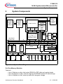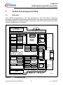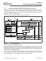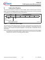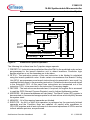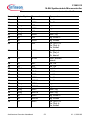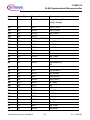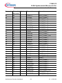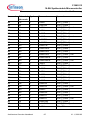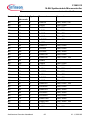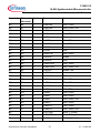
1
Architecture Overview Handbook, V1.1, Feb. 2006
C166S V2
16-Bit Synthesizable
Microcontroller
Microcontrollers
N e v e r
s t o p
t h i n k i n g .
Edition 2006-02
Published by Infineon Technologies AG,
St.-Martin-Strasse 53,
D-81541 München, Germany
© Infineon Technologies AG 2006.
All Rights Reserved.
Attention please!
The information herein is given to describe certain components and shall not be considered as warranted
characteristics.
Terms of delivery and rights to technical change reserved.
We hereby disclaim any and all warranties, including but not limited to warranties of non-infringement, regarding
circuits, descriptions and charts stated herein.
Infineon Technologies is an approved CECC manufacturer.
Information
For further information on technology, delivery terms and conditions and prices please contact your nearest
Infineon Technologies Office in Germany or our Infineon Technologies Representatives worldwide.
Warnings
Due to technical requirements components may contain dangerous substances. For information on the types in
question please contact your nearest Infineon Technologies Office.
Infineon Technologies Components may only be used in life-support devices or systems with the express written
approval of Infineon Technologies, if a failure of such components can reasonably be expected to cause the failure
of that life-support device or system, or to affect the safety or effectiveness of that device or system. Life support
devices or systems are intended to be implanted in the human body, or to support and/or maintain and sustain
and/or protect human life. If they fail, it is reasonable to assume that the health of the user or other persons may
be endangered.
Architecture Overview Handbook, V1.1, Feb. 2006
C166S V2
16-Bit Synthesizable
Microcontroller
Microcontrollers
N e v e r
s t o p
t h i n k i n g .
C166S V2 Architecture Overview Handbook
Revision History:
2006-02
Previous Version:
none
Page
V1.1
Subjects (major changes since last revision)
Reissue. Updated Instruction Set Summary
C166® is a registered trademark of Infineon Technologies AG.
We Listen to Your Comments
Any information within this document that you feel is wrong, unclear or missing?
Your feedback will help us to continuously improve the quality of this document.
Please send your proposal (including a reference to this document) to:
[email protected]
C166S V2
16-Bit Synthesizable Microcontroller
1
1.1
1.2
1.3
Preface . . . . . . . . . . . . . . . . . . . . . . . . . . . . . . . . . . . . . . . . . . . . . . . . . . . .
Overview . . . . . . . . . . . . . . . . . . . . . . . . . . . . . . . . . . . . . . . . . . . . . . . . . . .
Technical Summary . . . . . . . . . . . . . . . . . . . . . . . . . . . . . . . . . . . . . . . . . . .
Target Applications . . . . . . . . . . . . . . . . . . . . . . . . . . . . . . . . . . . . . . . . . . .
2
System Components . . . . . . . . . . . . . . . . . . . . . . . . . . . . . . . . . . . . . . . . . 8
3
3.1
3.2
3.3
3.4
3.5
3.6
3.7
3.8
Central Processing Unit (CPU) . . . . . . . . . . . . . . . . . . . . . . . . . . . . . . . .
Overview . . . . . . . . . . . . . . . . . . . . . . . . . . . . . . . . . . . . . . . . . . . . . . . . . .
CPU Special Function Registers (SFRs) . . . . . . . . . . . . . . . . . . . . . . . . . .
Instruction Fetch Unit (IFU) & Program Flow Control . . . . . . . . . . . . . . . .
Code Addressing via Code Segment & Instruction Pointers . . . . . . . . . . .
General Purpose Registers (GPR) . . . . . . . . . . . . . . . . . . . . . . . . . . . . . .
Context Switch . . . . . . . . . . . . . . . . . . . . . . . . . . . . . . . . . . . . . . . . . . . . . .
System Stack . . . . . . . . . . . . . . . . . . . . . . . . . . . . . . . . . . . . . . . . . . . . . . .
Data & DSP Addressing . . . . . . . . . . . . . . . . . . . . . . . . . . . . . . . . . . . . . .
12
12
14
15
16
17
19
19
20
4
4.1
4.2
4.3
4.4
4.5
4.6
4.7
Data Processing . . . . . . . . . . . . . . . . . . . . . . . . . . . . . . . . . . . . . . . . . . . .
Data Types . . . . . . . . . . . . . . . . . . . . . . . . . . . . . . . . . . . . . . . . . . . . . . . .
Constants . . . . . . . . . . . . . . . . . . . . . . . . . . . . . . . . . . . . . . . . . . . . . . . . . .
16-bit Add/Subtract, Barrel Shifter & Logic Unit . . . . . . . . . . . . . . . . . . . . .
Bit Manipulation Unit . . . . . . . . . . . . . . . . . . . . . . . . . . . . . . . . . . . . . . . . .
Multiply & Divide Unit . . . . . . . . . . . . . . . . . . . . . . . . . . . . . . . . . . . . . . . . .
Program Status Word (PSW) . . . . . . . . . . . . . . . . . . . . . . . . . . . . . . . . . . .
Parallel Data Processing . . . . . . . . . . . . . . . . . . . . . . . . . . . . . . . . . . . . . .
21
21
22
23
23
24
25
25
5
5.1
Memory Organization . . . . . . . . . . . . . . . . . . . . . . . . . . . . . . . . . . . . . . . 27
SFR Notes . . . . . . . . . . . . . . . . . . . . . . . . . . . . . . . . . . . . . . . . . . . . . . . . . 27
6
6.1
Instruction Pipeline . . . . . . . . . . . . . . . . . . . . . . . . . . . . . . . . . . . . . . . . . 28
Injected Instructions . . . . . . . . . . . . . . . . . . . . . . . . . . . . . . . . . . . . . . . . . . 30
7
7.1
7.2
Interrupt & Exception Handling . . . . . . . . . . . . . . . . . . . . . . . . . . . . . . . 31
Peripheral Event Controller (PEC) . . . . . . . . . . . . . . . . . . . . . . . . . . . . . . . 32
Priority, Arbitration & Structure . . . . . . . . . . . . . . . . . . . . . . . . . . . . . . . . . 33
8
External Bus Controller (EBC) . . . . . . . . . . . . . . . . . . . . . . . . . . . . . . . . 34
9
9.1
9.2
Instruction Set Summary . . . . . . . . . . . . . . . . . . . . . . . . . . . . . . . . . . . . 35
Instruction Mnemonics . . . . . . . . . . . . . . . . . . . . . . . . . . . . . . . . . . . . . . . . 35
Instruction Opcodes . . . . . . . . . . . . . . . . . . . . . . . . . . . . . . . . . . . . . . . . . . 49
Architecture Overview Handbook
3
4
5
6
7
V1.1, 2006-02
C166S V2
16-Bit Synthesizable Microcontroller
Preface
1
Preface
This document has been produced for engineering managers and hardware/software
engineers, to provide an overview of the C166S V2 architecture.
The C166S is the synthesizable version of the 16-bit C166 microcontroller family from
Infineon, one of the world’s most successful 16-bit architectures. It is designed to meet
the high performance requirements of real-time embedded control applications.
16-bit microcontrollers remain a strong force in the microprocessor market, providing a
compact, cost-competitive, high-performance alternative to the 32-bit architecture world.
Further information and documentation on the C166 product line (including the complete
C166S V2 User’s Manual), can be found on the Internet at:
http://www.infineon.com/xc166-family
Alternatively, contact your nearest Infineon Sales office to request more information.
Architecture Overview Handbook
4
V1.1, 2006-02
C166S V2
16-Bit Synthesizable Microcontroller
Preface
1.1
Overview
C166S V2 is the latest member of the C166 generation of microcontroller cores,
combining high performance with enhanced modular architecture. With its impressive
DSP performance and advanced interrupt handling features, the C166S V2 architecture
has been developed to provide a simple and straightforward migration from existing
C16x based applications.
The C166S V2 inherits the successful hardware and software system architecture
concepts established in the C16x 16-bit microcontroller families, while C166 code
compatibility enables re-use of existing code to dramatically reduce the time-to-market
for new product development.
The C166S V2 core is strategically placed for contemporary and emerging markets
dealing with performance-hungry, real-time applications.
Features include:
• High CPU performance - Single clock cycle execution doubles the performance at the
same CPU frequency (relative to the performance of the C166).
• Built-in advanced MAC (Multiply & Accumulate) unit dramatically increases DSP
performance.
• High Internal Program Memory bandwidth and use of the Instruction Fetch Pipeline to
significantly improve program flow regularity and optimize fetches into the Execution
Pipeline.
• Sophisticated Data Memory structure and multiple high-speed data buses, providing
transparent data access (0 cycles) and broad bandwidth for efficient DSP processing.
• Advanced exceptions handling block with multi-stage arbitration capability, to yield
dramatic interrupt performance with extremely small latency.
• Upgraded PEC (Peripheral Event Controller) supporting efficient and flexible DMA
(Direct Memory Access) features to support a broad range of fast peripherals.
• Highly modular architecture and flexible bus structure to provide effective methods of
integrating application-specific peripherals to produce customer-oriented derivatives.
Architecture Overview Handbook
5
V1.1, 2006-02
C166S V2
16-Bit Synthesizable Microcontroller
Preface
1.2
Technical Summary
Technical features of the C166S V2 architecture include:
• 7 stage Instruction Pipeline:
– 2-stage Instruction Fetch Pipeline with FIFO (First In First Out) for instruction
prefetching
– 5-stage Execution Pipeline
– Pipeline forwarding that controls data dependencies in hardware
• 16 Mbytes total linear address space for code and data (von Neumann architecture)
• Multiple, high bandwidth internal busses for data and instructions
• Enhanced memory map with extended I/O areas
• C16x family compatible on-chip Special Function Register (SFR) area
• Fast instruction execution
– Most instructions executed in one CPU clock cycle
– Fast multiplication (16-bit × 16-bit) in one CPU clock cycle
– MAC (Multiply & Accumulate) instructions executed in one CPU clock cycle
– Fast background execution of division (32-bit/16-bit) in 21 CPU clock cycles
– Zero cycle jump execution
• Enhanced boolean bit manipulation facilities
• Additional instructions to support HLL (High Level Language) and operating systems
• Register-based design with multiple variable register banks
– Two additional fast register banks
• General Purpose Register (GPR) architecture
– 16 GPRs for byte operands
– 16 GPRs for integer operands
• Overlapping 8-bit and 16-bit registers
• Opcode fully upward compatible with C166 family
• Variable stack with automatic stack overflow/underflow detection
• High performance branch, call and loop processing
• “Fast interrupt” and “Fast context switch” features
• Peripheral bus (PDBUS+) with bit protection
• Flexible PMU (Program Memory Unit) and DMU (Data Management Unit) with cache
capabilities
Architecture Overview Handbook
6
V1.1, 2006-02
C166S V2
16-Bit Synthesizable Microcontroller
Preface
1.3
Target Applications
The C166 architecture is firmly established in a diverse range of real-time embedded
control applications.
Optimization of the architecture for high instruction throughput and minimum response
time to external stimuli (such as interrupts), has resulted in the core being employed in
a wide variety of different application areas. These include:
Automotive
Telecom / Datacom
• Engine Management
• Communications Boards (LAN)
• Transmission Control
• Modems
• ABS / ASK
• PBX
• Active Suspension
• Mobile Communications
Industrial Control
EDP
• Robotics
• Hard Disk Drives
• PLCs
• Tape Drives
• Servo-Drives
• Printers
• Motor-Control
• Scanners
• Power-Inverters
• Digital Copiers
• Machine-Tool Control (CNC)
• FAX Machines
Consumer
• DVD / CD-Rom
• TV / Monitor
• VCR / Satellite Receiver
• Set Top Box
• Games
• Video Surveillance
Architecture Overview Handbook
7
V1.1, 2006-02
C166S V2
16-Bit Synthesizable Microcontroller
System Components
System Components
C166S V2 System
C166S V2 Core
Data
Memory
up to
24 Kbytes
SRAM
16
Program
Memory
Unit
(PMU)
64
64
Up to 3 Kbytes
DPRAM
C166S V2 CPU
Data
Management
Unit
Break Injection Trace
(DMU)
Interface Interface Interface
WDT
Interrupt Controller
&
Peripheral Event
Controller (PEC)
High Speed
System Bus
CGU
OSC
EBC
JTAG
Config. Block
External Bus Interface
PORT
Bus
JTAG
CONFIG
XTAL2
XTAL1
Dedicated Pins
NMI
PORT
OCDS
CLKOUT
Peripheral
1
...
Peripheral
n
16
Peripheral
2
PLL
16
PDBUS+
PORT
SCU
RESET
Program
Memory
up to
4 Mbytes
External
2
MCB05238
Figure 1
System Block Diagram
On-Chip Memory Modules
Features:
– Up to 3 Kbytes on-chip, dual ported SRAM for DSP data and register banks
– Up to 24 Kbytes on-chip, internal single ported SRAM module for data storage
– Up to 4 Mbytes on-chip, memory module for program storage
Architecture Overview Handbook
8
V1.1, 2006-02
C166S V2
16-Bit Synthesizable Microcontroller
System Components
Interrupt & PEC (Peripheral Event Controller)
Features:
– 16 priority-levels, applicable to 128 interrupt sources. Each priority level can be
further sub-divided into 4 or 8 sub-priorities (see Priority, Arbitration & Structure,
Page 33)
– 8 PEC channels with 24-bit Source & Destination Pointers & Segment Pointer
registers
– PEC data Source & Destination pointers can be simultaneously modified
– Independent programmable PEC level and “End of PEC” interrupt
(See also Peripheral Event Controller (PEC), Page 32)
Data Management Unit (DMU)
Handles all data transfers that are external to the core (i.e. external memory or on-chip
Special Function Registers on the PDBUS+). The DMU also controls instruction fetches
in external memory, acts as a data mover between the various interfaces and handles
access prioritization between EBC (External Bus Controller) accesses from the core and
the Program Memory Unit (PMU). This would be used for example, to allow an
instruction fetch from external memory in parallel with a data access that is not on the
EBC.
Program Memory Unit (PMU)
Provides the CPU with instructions and (via the DMU) with data located in the Internal
Program Memory. Instructions requested by the CPU can be located in the internal or
external memory. The Internal Program Memory is implemented within the PMU itself.
Multiply Accumulate Unit (MAC)
Features:
– Single cycle with zero cycle latency, including a 16 × 16 multiplier and 40-bit barrel
shifter. A single clock multiplication is calculated as ten times faster than C166 at
the same CPU clock speed
– 40-bit accumulator to handle overflows
– Automatic saturation to 32-bit, or rounding included with the MAC instruction
– Fractional numbers directly supported
– One, Finite Impulse Response (FIR) filter tap per cycle, with no circular buffer
management
Architecture Overview Handbook
9
V1.1, 2006-02
C166S V2
16-Bit Synthesizable Microcontroller
System Components
On-Chip Debug Support (OCDS - level 1) & JTAG
Features:
– Real-time emulation
– Extended trigger capability including: instruction pointer events, data events on
address and/or value, external inputs, counters, chaining of events and timers
– Software break support
– Break and “break before make” (on IP events only)
– Interrupt servicing during break or monitor mode
– Simple monitor mode or JTAG based debugging through instruction injection
Note: The C166S V2 OCDS is controlled by the debugger through a set of registers
accessible from the JTAG interface (Debugger refers to the tool connected to the
emulaton device). The OCDS receives information from the core (IP, data and
status for example) to monitor activity and generate triggers. The OCDS interacts
with the core through a break interface to suspend program execution and through
an injection interface to execute OCDS generated instructions.
External Bus Controller (EBC)
Performs all external memory and peripheral accesses. The EBC is controlled by a set
of configuration registers.
See External Bus Controller (EBC), Chapter 8 for more details.
System Control Unit (SCU)
Supports all central control tasks and all product specific features. Typically, the
following sub-modules are implemented:
– Reset Control
Controlled by the reset control unit.
– Power Saving Control
Manages idle, power down and sleep modes. The concrete definition of these
modes is product specific.
– ID Control
A set of six identification registers are defined for the most important silicon
parameters, including the chip manufacturer, the chip type and its properties.
These ID registers can be used for automatic test selection.
– External Interrupt Control
Fast, asynchronous, external interrupt inputs.
– Central System Control
Controls central system behaviour. The frequency of the PDBUS+ (bus clock) and
of all peripherals connected to it, is programmable according to maximum physical
bus speed and the application requirements. Clock generation status is also
Architecture Overview Handbook
10
V1.1, 2006-02
C166S V2
16-Bit Synthesizable Microcontroller
System Components
indicated. Various security levels, such as protected and unprotected mode, are
supported by the security level control state machine.
– WatchDog Timer (WDT)
A fail-safe mechanism to detect and prevent long term controller malfunctions.
Clock Generation Unit (CGU)
Uses either an oscillator or a crystal to generate the system clock. A programmable
on-chip Phase Locked Loop (PLL) adds high flexibility to clock generation.
On-Chip Bootstrap Loader
Allows the start code to be moved into internal RAM via the serial interface.
Architecture Overview Handbook
11
V1.1, 2006-02
C166S V2
16-Bit Synthesizable Microcontroller
Central Processing Unit (CPU)
3
Central Processing Unit (CPU)
3.1
Overview
The C166S V2 architecture is the third generation of the C166 family, combining
backward compatibility with powerful enhancements. This new architecture provides fast
and efficient access to different kinds of memories, high CPU performance and offers
excellent peripheral unit integration.
System Bus
PMU
Internal
Program Memory
Data Data Address
IN
OUT
CPU
Prefetch
Unit
CSP
IP
VECSEG
TFR
CPUCON1
Branch
Unit
2-Stage
Prefetch
Pipeline
CPUCON2
Return
Stack
5-Stage
Processing
Pipeline
Injection/
Exception
Handler
CPUID
FIFO
IFU
IPIP
IDX0
QR0
DPP0
SPSEG
IDX1
QR1
DPP1
SP
QX0
DPP2
STKOV
QX1
DPP3
STKUN
+/-
+/ADU
MRW
Multiply
Unit
Division Unit
Bit-Mask-Gen.
Multiply Unit
Barrel-Shifter
MCW
+/-
MSW
MAH
MAL
CP
Address
R15
R15
R14R15
R14
R14
R15
R14
GPRs
GPRs
GPRs
GPRs
R1
R1
R0 R1
R0
R0
R1
R0
MDC
+/-
PSW
MDH
MDL
ZEROS
ONES
RF
Buffer
MAC
ALU
Data IN
Data OUT
WB
Data Data
Data Data
IN
OUT Address IN
OUT Address
SRAM
DMU
Figure 2
DPRAM
Peripheral Bus
System Bus
MCA05239
CPU Architecture
Architecture Overview Handbook
12
V1.1, 2006-02
C166S V2
16-Bit Synthesizable Microcontroller
Central Processing Unit (CPU)
The new architecture gives higher CPU clock frequencies and reduces the number of
clock cycles per executed instruction by half, when compared with the C166 Core. The
integration of a Multiplication & Accumulation (MAC) unit has also dramatically increased
the performance of DSP-intensive tasks.
The eight main units of the C166S V2 listed below, have been optimized to achieve
maximum performance and flexibility:
1. High Performance Instruction Fetch Unit (IFU)
– High Bandwidth Fetch Interface
– Instruction FIFO
– High Performance Branch, Call and Loop-Processing with instruction flow
prediction
2. Return Stack
– Injection/Exception Handler
– Handling of Interrupt Requests
– Handling of Hardware Failures
3. Instruction Pipeline (IPIP)
– By-passable, 2-stage Prefetch Pipeline
– 5-stage Execution Pipeline
4. Address & Data Unit (ADU)
– 16-bit arithmetic unit for address generation
– DSP address unit with a set of dedicated address and offset pointers
5. Arithmetic & Logic Unit (ALU)
– 8-bit and 16-bit Arithmetic Unit
– 16-bit Barrel Shifter
– Multiplication & Division Unit
– 8-bit and 16-bit Logic Unit
– Bit manipulation Unit
6. Multiply & Accumulate Unit (MAC)
– 16-bit multiplier with 32-bit result generation1)
– 40-bit Accumulator with 40-bit Barrel Shifter
– Repeat Control Unit
7. Register File (RF)
– 5-port Register File with three independent register banks
8. Write Back Buffer (WB)
– 3-entry buffer
1)
The same hardware-multiplier is used in the ALU and MAC Units.
Architecture Overview Handbook
13
V1.1, 2006-02
C166S V2
16-Bit Synthesizable Microcontroller
Central Processing Unit (CPU)
3.2
CPU Special Function Registers (SFRs)
The core CPU requires a set of CPU Special Function Registers (CSFRs). These
registers have the following functions:
•
•
•
•
•
•
To maintain system state information
To control both system and bus configuration
To manage code memory segmentation and data memory paging
To access the General Purpose Registers (GPRs) and the System Stack
To supply the ALU (Arithmetic & Logic Unit) with register-addressable constants
To support ALU multiply and divide operations
CPU SFRs can be controlled by any instruction capable of addressing the SFR memory
space, so there is no need for special system control instructions. However, restrictions
have been imposed on user access to some CSFRs, to ensure proper processor
operation. The Instruction Pointer (IP) and Code Segment Pointer (CSP) cannot be
accessed directly for example, but can only be changed indirectly via branch
instructions.
The PSW (Program Status Word), SP (Stack Pointer) and MDC (Multiply Divide Control)
registers can be modified explicitly by the programmer, but also implicitly by the CPU
during normal instruction processing.
Architecture Overview Handbook
14
V1.1, 2006-02
C166S V2
16-Bit Synthesizable Microcontroller
Central Processing Unit (CPU)
3.3
Instruction Fetch Unit (IFU) & Program Flow Control
The Instruction Fetch Unit (IFU) prefetches and pre-processes instructions to provide a
continuous instruction flow. The IFU can simultaneously prefetch at least two instructions
from the Program Memory Unit (PMU) via a 64-bit wide bus, storing them in an
instruction FIFO (First In First Out).
The IFU contains two pipeline stages - Prefetch and Fetch:
64-Bit
Data
Instruction Buffer (up to 6 Instructions)
IFU IFU
Control Pipeline
24-Bit
Address
CSP
+/-
Prefetch
Stage
IP
Branch Detection and Prediction Logic
Return Stack
CPUCON2
BFU (Branch
Folding Unit)
Control
Registers
Instruction FIFO
(First In First Out)
CPUID
Injection and Exception
Handler
VECSEG
TFR
Bypass Prefetch to Decode
CPUCON1
Bypass Fetch to Decode
Instruction Buffer (up to 3 Instructions)
Fetch
Stage
Instruction Buffer (1 Instruction)
Decode Stage
MCB05240
Figure 3
IFU Block Diagram
See also Chapter 6, Instruction Pipeline.
During the Prefetch stage, the Branch Detection and Prediction Logic analyze up to three
prefetched instructions stored in the first Instruction Buffer (which can hold up to six
instructions). If a branch is detected, then the IFU initiates a fetch of the next instruction
from the PMU using prediction rules.
After analysis in the Prefetch Stage, a maximum of three instructions can be stored in
the second Instruction Buffer. This second Buffer is the input register for the Fetch Stage.
At the Fetch Stage, instructions are stored in an instruction FIFO.
Architecture Overview Handbook
15
V1.1, 2006-02
C166S V2
16-Bit Synthesizable Microcontroller
Central Processing Unit (CPU)
In the Fetch Stage the Branch Folding Unit (BFU) processes branch instructions in
parallel with preceding instructions, by pre-processing and re-formatting the branch
instruction.
The BFU defines (calculates) the absolute target address and then combines that with
the branch condition and branch attribute bits. This information is then stored in the same
FIFO step as the preceding instruction. The target address is also used to calculate and
prefetch the next instruction.
By pre-processing branch instructions the instruction flow can be predicted. While the
CPU is in the process of executing an instruction fetched from the FIFO, the IFU Prefetch
stage starts to fetch a new instruction from the PMU at a predicted target address. The
latency time of this access is hidden by executing the previously buffered instructions in
the FIFO. In this way, even when handling non-sequential instructions, the IFU usually
provides a continuous instruction flow.
The Execution Pipeline fetches both instructions from the FIFO and these are executed
in parallel. If the instruction flow was predicted incorrectly or if the FIFO is empty, the two
IFU stages can be bypassed.
3.4
Code Addressing via Code Segment & Instruction Pointers
The C166S V2 CPU has a total addressable memory space of 16 Mbytes. This address
space is arranged as 256 segments of 64 Kbytes each.
A dedicated 24-bit code address pointer is used to access the memories for instruction
fetches. This pointer has two parts:
– An 8-bit Code Segment Pointer (CSP)
– A 16-bit offset called the Instruction Pointer (IP)
Concatenation of the CSP and IP results in a correct 24-bit physical memory address.
Memory organized
in segments
255
FF'0000H
254
FE'0000H
1
01'0000H
0
00'0000H
15
8 7
0
15
CSP
0
IP
16 15
23
Segment
0
Offset
MCA05241
Figure 4
Addressing via the Code Segment Pointer & Instruction Pointer
Architecture Overview Handbook
16
V1.1, 2006-02
C166S V2
16-Bit Synthesizable Microcontroller
Central Processing Unit (CPU)
3.5
General Purpose Registers (GPR)
The C166S V2 CPU uses banks of sixteen dedicated registers (R0 through to R15),
called General Purpose Registers (GPRs). These banks can be accessed in one CPU
cycle. The GPRs are the working registers of the Arithmetic and Logic Unit (ALU), and
also serve as address pointers for indirect addressing modes.
Several banks of GPRs are memory mapped, although two ‘local’ banks are not
memory-mapped (see the Register File (RF) description in this section). The banks of
the memory-mapped GPRs are located in the internal DPRAM (Dual-Ported RAM). One
bank uses a block of 16 consecutive words. A Context Pointer (CP) register determines
the base address of the currently selected bank.
Because of the required number of access ports and access time, the GPRs located in
the DPRAM cannot be accessed directly. To get the required performance, the GPRs
are cached in a 5-port Register File for high speed access.
Register File (RF)
The Register File is split into three independent physical register banks, consisting of
1 Global and 2 Local banks:
Architecture Overview Handbook
17
V1.1, 2006-02
C166S V2
16-Bit Synthesizable Microcontroller
Central Processing Unit (CPU)
Core-RAM
Register File (RF)
Global
Local
AGU Write Port
Memory Mapped GPR Bank
ALU Write Port
R15
R14
R1
R0
Context
Pointer
(CP)
R15
R15
R14
R13
R12
R11
R10
R9
R8
R7
R6
R5
R4
R3
R2
R1
R0
R15
R14
R13
R12
R11
R10
R9
R8
R7
R6
R5
R4
R3
R2
R1
R0
2 Local Banks
AGU Read Port
ALU Read Port 1
ALU Read Port 2
MCA05242
Figure 5
Register File
The memory-mapped GPR bank selected by the current Context Pointer (CP) is always
cached in the Global register bank. Only one memory-mapped GPR bank can be cached
at any one time. In the case of a context switch, the cache contents must be sequentially
saved and restored.
Note: The Global register bank is the equivalent of the memory-mapped GPR bank of
the C166 family, selected by the Context Pointer.
To support a very fast context switch for time-critical tasks, two independent, nonmemory mapped GPR banks are available. These 2 banks are physically and logically
located in the two Local register banks. Local GPRs can be accessed via 4 or 8-bit
register addresses, after a Local bank is selected within the Program Status Word
(PSW).
Architecture Overview Handbook
18
V1.1, 2006-02
C166S V2
16-Bit Synthesizable Microcontroller
Central Processing Unit (CPU)
Only one of the three physical register banks can be activated at the same time, with
bank selection controlled by the BANK bitfield of the PSW.
The BANK bitfield can be changed explicitly by any instruction which writes to the PSW,
or implicitly by a RETI instruction (Return from Interrupt), an interrupt or hardware trap.
For interrupts, the selection of the register bank is configured in the Interrupt Controller
(ITC). Hardware traps always use the Global register bank.
3.6
Context Switch
An Interrupt Service Routine (ISR) or an operating system task schedule usually saves
all the used registers into the stack and restores them before returning. The more
registers a routine uses, the more time is required for saving and restoring.
There are two ways to switch a context in the C166S V2 core:
• By changing the selected register banks.
• Change the context of the Global register bank by changing the Context Pointer.
3.7
System Stack
A system stack of 64 Kbytes is supported. This stack can be located either externally, or
internally in one of the on-chip memories.
The 16-bit Stack Pointer (SP) Register addresses the stack within a 64 Kbyte segment.
The Stack Pointer Segment Register (SPSG) selects the segment in which the stack is
located.
A virtual stack (usually bigger then 64 Kbytes) can be implemented by software and is
supported by the Stack Overflow (STKOV) and Stack Underflow (STKUN) registers.
Architecture Overview Handbook
19
V1.1, 2006-02
C166S V2
16-Bit Synthesizable Microcontroller
Central Processing Unit (CPU)
3.8
Data & DSP Addressing
The Address Data Unit (ADU) contains two independent arithmetic units to generate,
calculate and update addresses for data accesses.
Address Data Unit tasks include:
• Data Paging (Standard Address Unit)
• Stack Handling (Standard Address Unit)
• Standard Address Generation (Standard Address Generation Unit)
The Standard Address Unit supports linear arithmetic for the indirect addressing
modes and also generates the address in the case of all other short and long
addressing modes.
• DSP Address Generation (DSP Address Unit)
The DSP Address Generation Unit contains an additional set of address pointers and
offset registers. An independent arithmetic unit allows the update of these dedicated
pointer registers in parallel with the GPR-Pointer modification of the Standard Address
Generation Unit. The DSP Address Generation Unit supports Indirect Addressing
modes that use the special pointer registers IDX0 and IDX1.
Architecture Overview Handbook
20
V1.1, 2006-02
C166S V2
16-Bit Synthesizable Microcontroller
Data Processing
4
Data Processing
All standard arithmetic, shift and logical operations are performed in the 16-bit Arithmetic
& Logic Unit (ALU). In addition to the standard ALU functions, the C166S V2 architecture
includes bit manipulation and multiply and divide units.
Most internal execution blocks have been optimized to perform operations on either 8-bit
or 16-bit numbers. After the pipeline has been filled, most instructions are completed in
one CPU cycle.
The status flags are automatically updated in the Program Status Word (PSW) register
after each ALU operation. These flags allow branching upon specific conditions. Both
signed and unsigned arithmetic support is provided via the user selectable branch test.
The status flags are also preserved automatically by the CPU upon entering an interrupt
or trap routine.
4.1
Data Types
The C166S Instruction Set supports operations on Booleans, bits, bit strings, characters,
integers and signed fractions. Most instructions work with a specific data type, while
others are useful for manipulating several data types:
Table 1
ANSI C Data Types
ANSI C Data Types
Size (Bytes) Range
CPU Data Format
bit
1-bit
0 or 1
BIT
sfrbit
1-bit
0 or 1
BIT
esfrbit
1-bit
0 or 1
BIT
signed char
1
-128 to +127
BYTE
unsigned char
1
0 to 255U
BYTE
sfr
1
0 to 65535U
WORD
esfr
1
0 to 65535U
WORD
signed short
2
-32768 to 32767
WORD
unsigned short
2
0 to 65535U
WORD
bitword
2
0 to 65535U
WORD or BIT
signed int
2
-32768 to 32767
WORD
unsigned int
2
0 to 65535U
WORD
signed long
4
-2147483648 to
+2147483647
Not directly supported
unsigned long
4
0 to 4294967295UL
Not directly supported
Architecture Overview Handbook
21
V1.1, 2006-02
C166S V2
16-Bit Synthesizable Microcontroller
Data Processing
Table 1
ANSI C Data Types (cont’d)
ANSI C Data Types
Size (Bytes) Range
float
4
±1.176E-38 to
±3.402E+38
Not directly supported
double
8
±2.225E-308 to
±1.797E+308
Not directly supported
long double
8
±2.225E-308 to
±1.797E+308
Not directly supported
near pointer
2
16/14-bits depending on WORD
memory model
far pointer
4
14-bits (16 k) in any
page
Table 2
CPU Data Format
Not directly supported
CPU Data Formats
CPU Data Format
Size (Bytes)
Range
BIT
1-bit
0 to 1
BYTES
1
0 to 255U or -128 to +127
WORD
2
0 to 65535U or -32768 to 32767
4.2
Constants
The CPU supports the use of wordwide and byteswide immediate constants. To
optimally utilize the available code storage area, these constants are represented in the
instruction formats by either 3, 4, 8 or 16-bits. Short constants are always zero-extended,
while long constants are truncated as necessary to match the data format for a given
operation.
Table 3
Constant Formats
Mnemonic
Word Operation
Byte Operation
#data3
0000H + data3
00H + data3
#data4
0000H + data4
00H + data4
#data8
0000H + data8
data8
#data16
data16
data16 ^ FFH
#mask
0000H + mask
mask
Note: Immediate Constants are always signified by a leading # sign.
Architecture Overview Handbook
22
V1.1, 2006-02
C166S V2
16-Bit Synthesizable Microcontroller
Data Processing
4.3
16-bit Add/Subtract, Barrel Shifter & Logic Unit
All standard arithmetic and logical operations are performed by the 16-bit Arithmetic &
Logic Unit (ALU).
For byte operations, the signals from bits 6 and 7 of the ALU result are used to control
the condition flags. Multiple precision arithmetic is supported by a “CARRY-IN” signal to
the ALU from previously calculated portions of the desired operation.
A 16-bit barrel shifter provides multiple bit shifts in a single cycle.
Rotations and arithmetic shifts are also supported.
4.4
Bit Manipulation Unit
Bit manipulation instructions enable the efficient control and testing of peripherals. One
advantage of the C166S V2 CPU over other microcontrollers, are instructions that
provide direct access to two operands in the bit addressable space, without having to be
first moved to temporary locations.
The same logical instructions that are available for words and bytes can also be used for
bits. It is possible to compare and modify a peripheral control bit in one instruction, while
multiple bit shift instructions are included to avoid long instruction streams of single bit
shift operations. These instructions require a single CPU cycle. In addition bit field
instructions are able to modify the multiple bits in one operand, in a single instruction.
All instructions that internally manipulate single bits or bit groups, use a
read-modify-write sequence that accesses the whole word containing the specified
bit(s). The consequences of this approach are:
• Bits are only modified within the internal address areas; i.e. internal RAM and SFRs.
External locations cannot be used with bit instructions.
– The upper 256 bytes of the SFR area, the Extended SFR (ESFR) area and the
internal RAM are bit addressable - those register bits located within the respective
sections can be directly manipulated using bit instructions.
– Other SFRs must be accessed byte/word wise.
Note: All GPRs are bit addressable independent of the allocation of the register bank,
via the Context Pointer (CP). Even GPRs allocated to RAM locations that are not
bit addressable provide this feature.
• For hardware affected bits, the hardware may change specific bits while the
read-modify-write operation is in progress. The write-back would overwrite the new bit
value generated by the hardware. A solution is achieved either through special
programming or by using the native hardware protection logic. This protection logic
guarantees that only the intended bit(s) is (are) effected by the write-back operation.
An example would be when hardware sets an interrupt request flag between the read
and write. If a conflict occurs between a hardware bit manipulation and an intended
software access, software has priority and determines the final bit value.
Architecture Overview Handbook
23
V1.1, 2006-02
C166S V2
16-Bit Synthesizable Microcontroller
Data Processing
4.5
Multiply & Divide Unit
The Multiply and Divide Unit consists of a fast 16 × 16-bit multiplier that executes a
multiplication in one CPU cycle, and a division sub-unit which performs the division
algorithm in a maximum of 21 CPU cycles, dependent on data type.
Note: The divide instruction requires 4 CPU cycles but then runs in the background while
further instructions are executed in parallel. New Multiply & Divide Unit instructions
are stalled until the current division is finished.
The unit executes Interrupt tasks immediately, while a current task is completed in the
background. If the Interrupt itself uses the Multiply & Divide Unit, then the flow of any
background task is also stalled. To avoid such stalls, the multiply and divide unit should
not be used during the first 14 CPU cycles of the Interrupt task.
The Multiply and Divide Unit uses the following registers:
• Multiply/Divide High (MDH) Register
– The 16-bit, non-bit addressable MDH register contains the high word of the 32-bit
Multiply/Divide (MD) register used by the CPU when it performs a multiplication or
a division using implicit addressing (DIV, DIVL, DIVLU, DIVU, MUL, MULU).
After an implicitly addressed multiplication, this register gives the high order sixteen
bits of the 32-bit result.
– For long divisions, MDH must be loaded with the high order sixteen bits of the 32-bit
dividend before the division has started.
– After any division, the MDH gives the 16-bit remainder.
• Multiply/Divide Low (MDL) Register
– The 16-bit, non-addressable MDL register contains the low word of the 32-bit
multiply/divide MD register used by the CPU when it performs a multiplication or a
division using implicit addressing (DIV, DIVL, DIVLU, DIVU, MUL, MULU).
After a multiplication MDL represents the low order sixteen bits of the 32-bit result.
– For long divisions MDL must be loaded with low order 16-bits of the 32-bit dividend
before the division has started.
– After any division MDL represents the 16-bit quotient.
• Multiply/Divide Control (MDC) Register
– The MDRIU flag of this bit addressable 16-bit register is used by the CPU when it
performs a multiplication or division in the ALU. This bit indicates MDL and MDH
register use, and must be sorted prior to each new multiplication or division
operation. The remaining portions of the register are not used.
Architecture Overview Handbook
24
V1.1, 2006-02
C166S V2
16-Bit Synthesizable Microcontroller
Data Processing
4.6
Program Status Word (PSW)
The PSW reflects the current CPU status. Two groups of bits represent the current ALU
status and current CPU interrupt status, while two separate bits (USR0 & USR1) can be
used as general purpose flags.
Condition flags within the PSW indicate the ALU status from the last ALU operation
(these flags are listed and explained in the C166S V2 User’s Manual). The condition
flags are set by specific rules dependent on the ALU operation or data movement.
4.7
Parallel Data Processing
Arithmetic instructions are performed in the Multiply & Accumulate (MAC) unit, with a
dedicated 40-bit wide Accumulator working register. Flags are used to allow branching
on specific conditions. The MAC provides single-cycle, non-pipelined instructions as:
•
•
•
•
•
32-bit addition
32-bit subtraction
Right & left shift
16-bit by 16-bit multiplication
16-bit by 16-bit multiplication with cumulative subtraction/addition
The major components of the MAC are:
•
•
•
•
•
•
•
16-bit by 16-bit signed/unsigned multiplier with signed result
Concatenation Unit
Scaler (one-bit left shifter) for fractional computing
40-bit Adder / Subtractor & 40-bit Signed Accumulator
Data Limiter
Accumulator Shifter
Repeat Counter
Architecture Overview Handbook
25
V1.1, 2006-02
C166S V2
16-Bit Synthesizable Microcontroller
Data Processing
16-Bit Input Operands
16
16
Repeat Counter
16
Concatenation Unit
MCW Register
16
Signed/Unsigned Multiplier
32
32
32
Signed
Ext.
40
40-Bit Adder/Subtracter
Round + Saturation
ACCU-Shifter
40
40-Bit Signed Accumulator
MSW Register
Limiter
Figure 6
40
40
MCA05243
Functional MAC Unit Block Diagram
Architecture Overview Handbook
26
V1.1, 2006-02
C166S V2
16-Bit Synthesizable Microcontroller
Memory Organization
5
Memory Organization
Memory space is configured in a “Von Neumann” architecture, which means that code
and data are accessed within the same linear address space. All of the physically
separated memory areas and external memory are mapped into a single common
address space.
The physically separated internal memory areas include:
•
•
•
•
•
ROM
Flash
DRAM (if integrated into a specific derivative of the C166S V2 Core)
RAM
Special Function Register Areas (SFRs & Extended SFRs)
The C166S V2 CPU has 16 Mbytes of total addressable memory space. This space is
arranged as 256 segments of 64 Kbytes each. Each segment is subdivided into four data
pages of 16 Kbytes each.
Most internal memory areas are mirrored into the system segment 0. The upper 4 Kbytes
of segment 0 (00’F000H to 00’FFFFH) hold the Special Function Register (SFR &
Extended SFR) and DPRAM areas.
Code may be stored in any memory area except for:
•
•
•
•
SFR blocks
DPRAM
Internal SRAM
I/O areas
These 4 areas may be used for control/data, but not for instructions.
Data may be stored in any memory area.
The 64 Kbyte memory area of segment 191 (BF’0000H to BF’FFFFH) is reserved for “on
chip” boot and debug/monitor program memories, so it cannot be used to store code or
data.
5.1
SFR Notes
• Any explicit write request to a SFR (via software), supersedes a simultaneous
hardware modification of the same register.
• All SFRs may be accessed wordwise or bytewise (some also bitwise).
• Reading bytes from word SFRs is a non-critical operation.
• Any write operation to a single SFR byte clears the non-addressed complementary
byte in the specified SFR.
• Non-implemented (reserved) SFR bits cannot be modified, and will always supply a
read value of 0.
Architecture Overview Handbook
27
V1.1, 2006-02
C166S V2
16-Bit Synthesizable Microcontroller
Instruction Pipeline
6
Instruction Pipeline
The Instruction pipeline is divided into seven stages, each of which process individual
tasks. The first two stages combine to operate as the Fetch process, with the remaining
five stages form the Processing section of the pipeline.
Fetch
Prefetch
Processing (Execution)
Fetch
Decode
Address
Memory
Execute
Write Back
Branch Detection
Unit
& Prediction Logic
Branch Folding Unit (BFU)
& FIFO (First In First Out)
Figure 7
MCA05244
Instruction Pipeline Stages
The Instruction Fetch stages prefetch instructions, storing them in an instruction FIFO
(First In, First Out). The pre-processing of branch instructions in combination with the
instruction FIFO allows the execution pipeline to be filled with a continuous flow of
instructions.
Note: In the case of an incorrectly predicted instruction flow, the instruction Fetch stages
are bypassed to reduce the number of dead cycles, but All instructions must pass
through each of the five Processing pipeline stages.
Architecture Overview Handbook
28
V1.1, 2006-02
C166S V2
16-Bit Synthesizable Microcontroller
Instruction Pipeline
6
Instruction Buffer (up to 6 Instructions)
Prefetch
Stage
Branch Detection and Prediction Logic
Instruction FIFO
(First In First Out)
Injection
and
Exception
Handler
Bypass Prefetch to Decode
Branch
Folding Unit
Bypass Fetch to Decode
Instruction Buffer (up to 3 Instructions)
Fetch
Stage
Instruction Buffer (1 Instruction)
Decode Stage
MCA05245
Figure 8
Instruction Pipeline Operation
The following list outlines how the 7 pipeline stages operate:
1. PREFETCH - Instructions are prefetched from the PMU in the predicted order and are
pre-processed in the branch detection unit to detect branches. Prediction logic
decides whether or not the branches are to be taken.
2. FETCH - The instruction pointer of the next instruction to be fetched is calculated
using the branch prediction rules. Under certain circumstances the Branch Folding
Unit (BFU), pre-processes some branch instructions to be executed in ‘zero-cycle’, by
combing/hooking them to the preceding instruction. Prefetched instructions are stored
in the instruction FIFO. At the same time instructions are transported out of the
instruction FIFO, to be executed in the instruction Processing stages.
3. DECODE - The instructions are decoded and, if required, the register file is accessed
to read the GPR (General Purpose Register) used in Indirect Addressing modes.
4. ADDRESS - All operand addresses are calculated. The Stack Pointer (SP) register is
decremented or incremented as appropriate for all instructions which implicitly access
the system stack.
5. MEMORY - All of the required operands are fetched.
6. EXECUTE - An ALU or MAC-Unit operation is performed on the previously fetched
operands and the Condition flags are updated. All explicit write operations to
CPU-SFR registers and all auto-increment or decrement operations of GPRs used as
indirect address pointers, are performed.
Architecture Overview Handbook
29
V1.1, 2006-02
C166S V2
16-Bit Synthesizable Microcontroller
Instruction Pipeline
7. WRITE BACK - All external operands and the remaining operands within the internal
DPRAM space are written back. Operands located in the internal SRAM are buffered
in the Write Back Buffer.
Because up to five different instructions can be processed simultaneously, the
C166S V2 CPU has additional dedicated hardware to deal with dependencies which
may exist between instructions in the different pipeline stages. This extra hardware
supports ‘forwarding’ of the operand read and write values. It also resolves most possible
conflicts in a time optimized fashion, without performance loss, such as the multiple use
of buses. Normally therefore, the user will be unaware of the various pipeline stages.
Only in some rare instances will the pipeline require attention by the programmer. In
these instances the delays caused by pipeline conflicts can then be used for other
instructions, to optimize performance.
Note: The C166S V2 has a fully interlocked pipeline. Instruction re-ordering is only
required for performance enhancement.
6.1
Injected Instructions
Injected Instructions are C166S V2-specific instructions, generated internally by the
machine. They are automatically injected into the DECODE stage, before passing
through the remaining pipeline stages as per a normal instruction.
These instructions are used to provide the time necessary to process instructions that
require more than one CPU cycle for processing.
Program interrupt, PEC transfer and OCE operations are also performed by injected
instructions.
Architecture Overview Handbook
30
V1.1, 2006-02
C166S V2
16-Bit Synthesizable Microcontroller
Interrupt & Exception Handling
7
Interrupt & Exception Handling
Advanced handling features and optimization of the C166S V2 architecture, with its
multi-layer arbitration and direct interrupt vector provision, have resulted in a dynamic
interrupt performance with extremely small latency.
The Interrupt and Exception Handler is responsible for managing all system and core
exceptions. These exceptions can be any of the following types:
• Interrupts generated by the Interrupt Controller (ITC)
• Direct Memory Access (DMA) transfers issued by the Peripheral Event Controller
(PEC)
• Software Traps caused by the TRAP instruction
• Hardware Traps issued by faults or specific system states
In normal processing the CPU temporarily suspends its current program execution and
branches to an Interrupt Service Routine (ISR) to service the device requesting an
interrupt, while the current program status is saved in the internal system stack.
The multi-layer prioritization scheme (see Priority, Arbitration & Structure, Page 33)
is applied to determine the order for handling multiple interrupt requests.
Software & Hardware Traps
Several hardware Trap functions are provided to handle erroneous conditions and
exceptions that may arise during program execution. A Trap can also be generated
externally by the Non-Maskable Interrupt pin (NMI). Hardware traps always have the
highest priority and prompt an immediate system response.
The software Trap function is invoked by the TRAP instruction that generates a software
interrupt for a specified interrupt vector.
For all Trap types, the current program status is saved in the system stack.
Architecture Overview Handbook
31
V1.1, 2006-02
C166S V2
16-Bit Synthesizable Microcontroller
Interrupt & Exception Handling
7.1
Peripheral Event Controller (PEC)
A faster alternative to normal interrupt processing uses the integrated Peripheral Event
Controller (PEC) to service a device requesting an interrupt. The PEC decides on the
CPU action required to manage a given request. This may be either a normal interrupt
service or a fast data transfer between two memory locations. The C166S V2 PEC
controls eight fast data transfer channels.
If a normal interrupt is requested, the CPU temporarily suspends the current program
execution and branches to an Interrupt Service Routine (ISR). The current program
status and context must be preserved, to be applied when the ISR finishes.
If a PEC channel is selected for servicing an interrupt request, a single word or byte data
transfer between any two memory locations is performed. During a PEC transfer, the
normal program execution of the CPU is halted and no internal program status
information needs to be saved.
The PEC transfer is the fastest possible interrupt response and often it is sufficient to
service a peripheral request.
PEC channels can perform the following actions:
• Byte or word transfer
• Continuous data transfer
• PEC channel-specific interrupt request upon data transfer completion
or
Common for all channels “End of PEC” interrupt for enhanced handling
• Automatic increment of Source and/or Destination pointers, with support of memory
to memory transfer (the Source and Destination pointers specify locations between
which data is to be moved).
• Channel Link Mode: PEC data transfers via a pair of PEC channels, that are switched
rotationally, to provide the possibility of data chaining.
Note: The interrupt prioritization scheme (see Priority, Arbitration & Structure,
Page 33) can also be applied to PEC interrupt handling.
PEC Control Registers
Each PEC channel is controlled by the respective PEC channel control register (PECCx)
and a set of 24-bit Source and Destination pointers:
Source = SRCPx Source, Destination = DSTPx, Segment Pointer = PECSEGx
(‘x’ stands for the PEC channel number)
The PECCx registers control the assignment of arbitration priority levels to the PEC
channels and the actions to be performed (see Priority, Arbitration & Structure,
Page 33).
Architecture Overview Handbook
32
V1.1, 2006-02
C166S V2
16-Bit Synthesizable Microcontroller
Interrupt & Exception Handling
7.2
Priority, Arbitration & Structure
The C166S V2 CPU offers up to 128 separate interrupt nodes. These 128 nodes can be
assigned to 16 possible interrupt priority levels. Each priority level can then be further
sub-divided into either:
• 4 sub-priorities, when using up to 64 interrupt nodes
• 8 sub-priorities, when using more than 64 interrupt nodes
Most interrupt sources or PEC requests are supplied with separate interrupt control
registers and interrupt vectors, to support modular and consistent software design
techniques.
The control register contains an interrupt request flag, enable bit and the interrupt priority
of the associated source. Each source request is activated by one specific event,
determined by the selected operating mode of the requesting device. In some cases,
multi-source interrupt nodes are incorporated for a more efficient use of system
resources. These nodes can be activated by various source requests.
All pending interrupt requests are arbitrated and the arbitration winner is sent to the CPU
together with its priority level and action request.
Note: The arbitration process starts with an interrupt request and stays active for as long
as an interrupt request is pending. If there are no pending requested, the
arbitration logic switches to the idle state to save power.
On receipt of the arbitration interrupt request winner, the CPU accepts an action request
if the requesting source has a higher priority than the current CPU priority level. If the
requesting source has a lower (or equal) interrupt priority than the current CPU task, it
remains pending.
The C166S V2 CPU operates a vectored interrupt system which reserves specific vector
locations in the memory space for the Reset, Trap and Interrupt service functions.
Whenever a request is made, the CPU branches to the location associated with the
respective interrupt source. The reserved vector locations build a jump table in the CPU
address space.
The type of actions the CPU will trigger from an interrupt request might include an
Interrupt, PEC or Jump Table Cache1) for example.
1)
Jump Table Cache (or Fast Interrupt): A set of 2 CPU registers which hold Interrupt Service Routine (ISR) start
addresses for two interrupt sources which have priority levels greater than or equal to 12. Use of this cache
avoids instruction fetches form the interrupt vector table and executes a direct jump to the ISR entry point.
Interrupt response time should therefore be significantly improved by using this cache.
Architecture Overview Handbook
33
V1.1, 2006-02
C166S V2
16-Bit Synthesizable Microcontroller
External Bus Controller (EBC)
8
External Bus Controller (EBC)
A powerful set of on-chip peripherals and on-chip program and data memories are
incorporated into the C166S V2 architecture, but these internal units only cover a small
fraction of the 16 Mbytes of available address space. External1) peripherals and
additional volatile and non-volatile memories can be incorporated into the system,
accessed via the External Bus interface. This interface has a number of configurations
so that it can be tailored to a given application system.
The integrated External Bus Controller (EBC) handles accesses to external memories or
peripherals. Its registers are functionally split into three groups:
• Mode registers - Used to program basic behaviour.
• Function, Timing & Address registers.
– Function registers specify the external bus cycles in terms of address
(MUX/DEMUX), data (16-bit/8-bit), chip select enable and READY control
– Timing configuration registers control the timing of the bus access and specify the
length of the different access phases
– Address Select registers define a specific address area for accesses
• Startup & Monitor Memory registers - Used to control the access to these dedicated
memories.
The External Bus Controller supports up to eight external chip select channels, each of
which is programmable via the Function & Timing registers.
There are 7 register sets of Function (FCONCS1 - 7), Timing (TCONCS1 - 7) and
Address (ADDRSEL 1 - 7) registers, with each set defining an independent ‘address
window’. External accesses outside these windows are controlled via the FCONCS0 and
TCONCS0 registers. Two additional chip select channels with fixed address ranges are
defined for the startup and the monitor memory.
External Bus timing is related to the reference clock output CLKOUT. All bus signals are
generated in relation to the rising edge of this clock. This behavior dramatically eases
the timing specification and allows high EBC operating frequencies above 100 MHz.
The External Bus protocol is compatible with the C16x protocols, but the External Bus
timing is improved in terms of wait state granularity. To support these improvements an
extended configuration scheme has been defined for C166S V2.
EBC configuration is carried out during the application initialization. This means that only
a small proportion of the initialization code has to be adapted to use the C166S V2 EBC
module instead of the C16x External Bus Controller.
1)
‘External’ in this context means ‘off-chip’ However, modules such as customer ASIC, startup memory,
additional peripherals and memories, can also be connected on-chip to the External Bus module. These
modules are, from the controller sub-system point of view, also external but on-chip.
Architecture Overview Handbook
34
V1.1, 2006-02
C166S V2
16-Bit Synthesizable Microcontroller
Instruction Set Summary
9
Instruction Set Summary
9.1
Instruction Mnemonics
This section summarizes the instructions and lists them by functional class. This enables
quick identification of the right instruction(s) for a specific function.
The following notes apply to this summary:
Data Addressing Modes
Rw:
Word GPR (R0, R1, … , R15)
Rb:
Byte GPR (RL0, RH0, …, RL7, RH7)
IDX:
Address Pointer IDX (IDX0, IDX1)
QX:
Address Offset Register QX (QX0, QX1)
QR:
Address Offset Register QR (QR0, QR1)
reg:
SFR or GPR
(in case of a byte operation on an SFR, only the low byte can be accessed via
‘reg’)
mem:
Direct word or byte memory location
[…]:
Indirect word or byte memory location
(Any word GPR can be used as indirect address pointer, except for the
arithmetic, logical and compare instructions, where only R0 to R3 are
allowed)
bitaddr Direct bit in the bit-addressable memory area
:
bitoff:
Direct word in the bit-addressable memory area
#data:
Immediate constant
(The number of significant bits which can be specified by the user is
represented by the respective appendix ’x’)
#mask8 Immediate 8-bit mask used for bit-field modifications
Table 9-1 shows the various combinations of pointer post-modification for the
addressing modes of the CoXXX instructions. The symbols “[Rwn*∗]” and “[IDXi∗]” will be
used to refer to these addressing modes.
Architecture Overview Handbook
35
V1.1, 2006-02
C166S V2
16-Bit Synthesizable Microcontroller
Instruction Set Summary
Table 9-1
Pointer Post-Modification Combinations for IDXi and Rwn
Symbol
Mnemonic
Address Pointer Operation
“[IDXi⊗]” stands for
[IDXi]
(IDXi) ← (IDXi) (no-operation)
[IDXi+]
(IDXi) ← (IDXi) +2 (i=0,1)
[IDXi -]
(IDXi) ← (IDXi) -2 (i=0,1)
[IDXi + QXj]
(IDXi) ← (IDXi) + (QXj) (i, j =0,1)
[IDXi - QXj]
(IDXi) ← (IDXi) - (QXj) (i, j =0,1)
“[Rwn⊗]” stands for
[Rwn]
(Rwn) ← (Rwn) (no-operation)
[Rwn+]
(Rwn) ← (Rwn) +2 (n=0-15)
[Rwn-]
(Rwn) ← (Rwn) -2 (n=0-15)
[Rwn+QRj]
(Rwn) ← (Rwn) + (QRj) (n=0-15;j =0,1)
[Rwn - QRj]
(Rwn) ← (Rwn) - (QRj) (n=0-15; j =0,1)
Multiply and Divide Operations
The MDL and MDH registers are implicit source and/or destination operands of the
multiply and divide instructions.
Branch Target Addressing Modes
caddr:
Direct 16-bit jump target address (Updates the Instruction Pointer)
seg:
Direct 2-bit segment address (Updates the Code Segment Pointer)
rel:
Signed 8-bit jump target word offset address relative to the Instruction
(Pointer of the following instruction)
#trap7:
Immediate 7-bit trap or interrupt number.
Extension Operations
#pag10: Immediate 10-bit page address.
#seg8:
Immediate 8-bit segment address.
The EXT* instructions override the standard DPP addressing scheme.
Architecture Overview Handbook
36
V1.1, 2006-02
C166S V2
16-Bit Synthesizable Microcontroller
Instruction Set Summary
Branch Condition Codes
cc:Symbolically specifiable condition codes
cc_UC
Unconditional
cc_Z
Zero
cc_NZ
Not Zero
cc_V
Overflow
cc_NV
No Overflow
cc_N
Negative
cc_NN
Not Negative
cc_C
Carry
cc_NC
No Carry
cc_EQ
Equal
cc_NE
Not Equal
cc_ULT
Unsigned Less Than
cc_ULE
Unsigned Less Than or Equal
cc_UGE
Unsigned Greater Than or Equal
cc_UGT
Unsigned Greater Than
cc_SLE
Signed Less Than or Equal
cc_SGE
Signed Greater Than or Equal
cc_SGT
Signed Greater Than
cc_NET
Not Equal and Not End-of-Table
cc_nusr0
USR-bit 0 is cleared1)
cc_nusr1
USR-bit 1 is cleared1)
cc_usr0
USR-bit 0 is set1)
cc_usr1
USR-bit 1 is set1)
1)
Only usable with the JMPA and CALLA instructions
Architecture Overview Handbook
37
V1.1, 2006-02
C166S V2
16-Bit Synthesizable Microcontroller
Instruction Set Summary
Table 9-2
Instruction Set Summary
Mnemonic
Description
Byte
s
Arithmetic Operations
ADD Rw, Rw
Add direct word GPR to direct GPR
2
ADD Rw, [Rw]
Add indirect word memory to direct GPR
2
ADD Rw, [Rw +]
Add indirect word memory to direct GPR and postincrement source pointer by 2
2
ADD Rw, #data3
Add immediate word data to direct GPR
2
ADD reg, #data16
Add immediate word data to direct register
4
ADD reg, mem
Add direct word memory to direct register
4
ADD mem, reg
Add direct word register to direct memory
4
ADDB Rb, Rb
Add direct byte GPR to direct GPR
2
ADDB Rb, [Rw]
Add indirect byte memory to direct GPR
2
ADDB Rb, [Rw +]
Add indirect byte memory to direct GPR and
post-increment source pointer by 1
2
ADDB Rb, #data3
Add immediate byte data to direct GPR
2
ADDB reg, #data8
Add immediate byte data to direct register
4
ADDB reg, mem
Add direct byte memory to direct register
4
ADDB mem, reg
Add direct byte register to direct memory
4
ADDC Rw, Rw
Add direct word GPR to direct GPR with Carry
2
ADDC Rw, [Rw]
Add indirect word memory to direct GPR with Carry
2
ADDC Rw, [Rw +]
Add indirect word memory to direct GPR with Carry
and post-increment source pointer by 2
2
ADDC Rw, #data3
Add immediate word data to direct GPR with Carry
2
ADDC reg, #data16
Add immediate word data to direct register with Carry 4
ADDC reg, mem
Add direct word memory to direct register with Carry 4
ADDC mem, reg
Add direct word register to direct memory with Carry 4
ADDCB Rb, Rb
Add direct byte GPR to direct GPR with Carry
2
ADDCB Rb, [Rw]
Add indirect byte memory to direct GPR with Carry
2
ADDCB Rb, [Rw +]
Add indirect byte memory to direct GPR with Carry
and post-increment source pointer by 1
2
ADDCB Rb, #data3
Add immediate byte data to direct GPR with Carry
2
Architecture Overview Handbook
38
V1.1, 2006-02
C166S V2
16-Bit Synthesizable Microcontroller
Instruction Set Summary
Table 9-2
Instruction Set Summary (cont’d)
Mnemonic
Description
Byte
s
ADDCB reg, #data8
Add immediate byte data to direct register with Carry 4
ADDCB reg, mem
Add direct byte memory to direct register with Carry
4
ADDCB mem, reg
Add direct byte register to direct memory with Carry
4
SUB Rw, Rw
Subtract direct word GPR from direct GPR
2
SUB Rw, [Rw]
Subtract indirect word memory from direct GPR
2
SUB Rw, [Rw +]
Subtract indirect word memory from direct GPR and
post-increment source pointer by 2
2
SUB Rw, #data3
Subtract immediate word data from direct GPR
2
SUB reg, #data16
Subtract immediate word data from direct register
4
SUB reg, mem
Subtract direct word memory from direct register
4
SUB mem, reg
Subtract direct word register from direct memory
4
SUBB Rb, Rb
Subtract direct byte GPR from direct GPR
2
SUBB Rb, [Rw]
Subtract indirect byte memory from direct GPR
2
SUBB Rb, [Rw +]
Subtract indirect byte memory from direct GPR and
post-increment source pointer by 1
2
SUBB Rb, #data3
Subtract immediate byte data from direct GPR
2
SUBB reg, #data8
Subtract immediate byte data from direct register
4
SUBB reg, mem
Subtract direct byte memory from direct register
4
SUBB mem, reg
Subtract direct byte register from direct memory
4
SUBC Rw, Rw
Subtract direct word GPR from direct GPR with Carry 2
SUBC Rw, [Rw]
Subtract indirect word memory from direct GPR with 2
Carry
SUBC Rw, [Rw +]
Subtract indirect word memory from direct GPR with 2
Carry and post-increment source pointer by 2
SUBC Rw, #data3
Subtract immediate word data from direct GPR with
Carry
2
SUBC reg, #data16
Subtract immediate word data from direct register
with Carry
4
SUBC reg, mem
Subtract direct word memory from direct register with 4
Carry
SUBC mem, reg
Subtract direct word register from direct memory with 4
Carry
Architecture Overview Handbook
39
V1.1, 2006-02
C166S V2
16-Bit Synthesizable Microcontroller
Instruction Set Summary
Table 9-2
Instruction Set Summary (cont’d)
Mnemonic
Description
Byte
s
SUBCB Rb, Rb
Subtract direct byte GPR from direct GPR with Carry 2
SUBCB Rb, [Rw]
Subtract indirect byte memory from direct GPR with
Carry
2
SUBCB Rb, [Rw +]
Subtract indirect byte memory from direct GPR with
Carry
and post-increment source pointer by 1
2
SUBCB Rb, #data3
Subtract immediate byte data from direct GPR with
Carry
2
SUBCB reg, #data8
Subtract immediate byte data from direct register with 4
Carry
SUBCB reg, mem
Subtract direct byte memory from direct register with 4
Carry
SUBCB mem, reg
Subtract direct byte register from direct memory with 4
Carry
MUL Rw, Rw
Signed multiply direct GPR by direct GPR (16-16-bit) 2
MULU Rw, Rw
Unsigned multiply direct GPR by direct GPR (16-16- 2
bit)
DIV Rw
Signed divide register MDL by direct GPR (16-/16-bit) 2
DIVL Rw
Signed long divide register MD by direct GPR (32-/16- 2
bit)
DIVLU Rw
Unsigned long divide register MD by direct GPR
(32-/16-bit)
DIVU Rw
Unsigned divide register MDL by direct GPR (16-/16- 2
bit)
CPL Rw
Complement direct word GPR
2
CPLB Rb
Complement direct byte GPR
2
NEG Rw
Negate direct word GPR
2
NEGB Rb
Negate direct byte GPR
2
AND Rw, Rw
Bitwise AND direct word GPR with direct GPR
2
AND Rw, [Rw]
Bitwise AND indirect word memory with direct GPR
2
2
Logical Instructions
Architecture Overview Handbook
40
V1.1, 2006-02
C166S V2
16-Bit Synthesizable Microcontroller
Instruction Set Summary
Table 9-2
Instruction Set Summary (cont’d)
Mnemonic
Description
Byte
s
AND Rw, [Rw +]
Bitwise AND indirect word memory with direct GPR
and
post-increment source pointer by 2
2
AND Rw, #data3
Bitwise AND immediate word data with direct GPR
2
AND reg, #data16
Bitwise AND immediate word data with direct register 4
AND reg, mem
Bitwise AND direct word memory with direct register
4
AND mem, reg
Bitwise AND direct word register with direct memory
4
ANDB Rb, Rb
Bitwise AND direct byte GPR with direct GPR
2
ANDB Rb, [Rw]
Bitwise AND indirect byte memory with direct GPR
2
ANDB Rb, [Rw +]
Bitwise AND indirect byte memory with direct GPR
and post-increment source pointer by 1
2
ANDB Rb, #data3
Bitwise AND immediate byte data with direct GPR
2
ANDB reg, #data8
Bitwise AND immediate byte data with direct register 4
ANDB reg, mem
Bitwise AND direct byte memory with direct register
4
ANDB mem, reg
Bitwise AND direct byte register with direct memory
4
OR Rw, Rw
Bitwise OR direct word GPR with direct GPR
2
OR Rw, [Rw]
Bitwise OR indirect word memory with direct GPR
2
OR Rw, [Rw +]
Bitwise OR indirect word memory with direct GPR
and post-increment source pointer by 2
2
OR Rw, #data3
Bitwise OR immediate word data with direct GPR
2
OR reg, #data16
Bitwise OR immediate word data with direct register
4
OR reg, mem
Bitwise OR direct word memory with direct register
4
OR mem, reg
Bitwise OR direct word register with direct memory
4
ORB Rb, Rb
Bitwise OR direct byte GPR with direct GPR
2
ORB Rb, [Rw]
Bitwise OR indirect byte memory with direct GPR
2
ORB Rb, [Rw +]
Bitwise OR indirect byte memory with direct GPR and 2
post-increment source pointer by 1
ORB Rb, #data3
Bitwise OR immediate byte data with direct GPR
2
ORB reg, #data8
Bitwise OR immediate byte data with direct register
4
ORB reg, mem
Bitwise OR direct byte memory with direct register
4
ORB mem, reg
Bitwise OR direct byte register with direct memory
4
Architecture Overview Handbook
41
V1.1, 2006-02
C166S V2
16-Bit Synthesizable Microcontroller
Instruction Set Summary
Table 9-2
Instruction Set Summary (cont’d)
Mnemonic
Description
Byte
s
XOR Rw, Rw
Bitwise XOR direct word GPR with direct GPR
2
XOR Rw, [Rw]
Bitwise XOR indirect word memory with direct GPR
2
XOR Rw, [Rw +]
Bitwise XOR indirect word memory with direct GPR
and post-increment source pointer by 2
2
XOR Rw, #data3
Bitwise XOR immediate word data with direct GPR
2
XOR reg, #data16
Bitwise XOR immediate word data with direct register 4
XOR reg, mem
Bitwise XOR direct word memory with direct register 4
XOR mem, reg
Bitwise XOR direct word register with direct memory 4
XORB Rb, Rb
Bitwise XOR direct byte GPR with direct GPR
2
XORB Rb, [Rw]
Bitwise XOR indirect byte memory with direct GPR
2
XORB Rb, [Rw +]
Bitwise XOR indirect byte memory with direct GPR
and post-increment source pointer by 1
2
XORB Rb, #data3
Bitwise XOR immediate byte data with direct GPR
2
XORB reg, #data8
Bitwise XOR immediate byte data with direct register 4
XORB reg, mem
Bitwise XOR direct byte memory with direct register
4
XORB mem, reg
Bitwise XOR direct byte register with direct memory
4
Boolean Bit Manipulation Operations
BCLR bitaddr
Clear direct bit
2
BSET bitaddr
Set direct bit
2
BMOV bitaddr, bitaddr
Move direct bit to direct bit
4
BMOVN bitaddr, bitaddr
Move negated direct bit to direct bit
4
BAND bitaddr, bitaddr
AND direct bit with direct bit
4
BOR bitaddr, bitaddr
OR direct bit with direct bit
4
BXOR bitaddr, bitaddr
XOR direct bit with direct bit
4
BCMP bitaddr, bitaddr
Compare direct bit to direct bit
4
BFLDH bitoff, #mask8,
#data8
Bitwise modify masked high byte of bit-addressable
direct word memory with immediate data
4
BFLDL bitoff, #mask8,
#data8
Bitwise modify masked low byte of bit-addressable
direct word memory with immediate data
4
CMP Rw, Rw
Compare direct word GPR to direct GPR
2
Architecture Overview Handbook
42
V1.1, 2006-02
C166S V2
16-Bit Synthesizable Microcontroller
Instruction Set Summary
Table 9-2
Instruction Set Summary (cont’d)
Mnemonic
Description
Byte
s
CMP Rw, [Rw]
Compare indirect word memory to direct GPR
2
CMP Rw, [Rw +]
Compare indirect word memory to direct GPR and
post-increment source pointer by 2
2
CMP Rw, #data3
Compare immediate word data to direct GPR
2
CMP reg, #data16
Compare immediate word data to direct register
4
CMP reg, mem
Compare direct word memory to direct register
4
CMPB Rb, Rb
Compare direct byte GPR to direct GPR
2
CMPB Rb, [Rw]
Compare indirect byte memory to direct GPR
2
CMPB Rb, [Rw +]
Compare indirect byte memory to direct GPR and
post-increment source pointer by 1
2
CMPB Rb, #data3
Compare immediate byte data to direct GPR
2
CMPB reg, #data8
Compare immediate byte data to direct register
4
CMPB reg, mem
Compare direct byte memory to direct register
4
Compare and Loop Control Instructions
CMPD1 Rw, #data4
Compare immediate word data to direct GPR and
decrement GPR by 1
2
CMPD1 Rw, #data16
Compare immediate word data to direct GPR and
decrement GPR by 1
4
CMPD1 Rw, mem
Compare direct word memory to direct GPR and
decrement GPR by 1
4
CMPD2 Rw, #data4
Compare immediate word data to direct GPR and
decrement GPR by 2
2
CMPD2 Rw, #data16
Compare immediate word data to direct GPR and
decrement GPR by 2
4
CMPD2 Rw, mem
Compare direct word memory to direct GPR and
decrement GPR by 2
4
CMPI1 Rw, #data4
Compare immediate word data to direct GPR and
increment GPR by 1
2
CMPI1 Rw, #data16
Compare immediate word data to direct GPR and
increment GPR by 1
4
Architecture Overview Handbook
43
V1.1, 2006-02
C166S V2
16-Bit Synthesizable Microcontroller
Instruction Set Summary
Table 9-2
Instruction Set Summary (cont’d)
Mnemonic
Description
Byte
s
CMPI1 Rw, mem
Compare direct word memory to direct GPR and
increment GPR by 1
4
CMPI2 Rw, #data4
Compare immediate word data to direct GPR and
increment GPR by 2
2
CMPI2 Rw, #data16
Compare immediate word data to direct GPR and
increment GPR by 2
4
CMPI2 Rw, mem
Compare direct word memory to direct GPR and
increment GPR by 2
4
Determine number of shift cycles to normalize direct
word GPR and store result in direct word GPR
2
Prioritize Instruction
PRIOR Rw, Rw
Shift and Rotate Instructions
SHL Rw, Rw
Shift left direct word GPR;
number of shift cycles specified by direct GPR
2
SHL Rw, #data4
Shift left direct word GPR;
number of shift cycles specified by immediate data
2
SHR Rw, Rw
Shift right direct word GPR;
number of shift cycles specified by direct GPR
2
SHR Rw, #data4
Shift right direct word GPR;
number of shift cycles specified by immediate data
2
ROL Rw, Rw
Rotate left direct word GPR;
number of shift cycles specified by direct GPR
2
ROL Rw, #data4
Rotate left direct word GPR;
number of shift cycles specified by immediate data
2
ROR Rw, Rw
Rotate right direct word GPR;
number of shift cycles specified by direct GPR
2
ROR Rw, #data4
Rotate right direct word GPR;
number of shift cycles specified by immediate data
2
ASHR Rw, Rw
Arithmetic (sign bit) shift right direct word GPR;
number of shift cycles specified by direct GPR
2
Architecture Overview Handbook
44
V1.1, 2006-02
C166S V2
16-Bit Synthesizable Microcontroller
Instruction Set Summary
Table 9-2
Instruction Set Summary (cont’d)
Mnemonic
Description
Byte
s
ASHR Rw, #data4
Arithmetic (sign bit) shift right direct word GPR;
number of shift cycles specified by immediate data
2
MOV Rw, Rw
Move direct word GPR to direct GPR
2
MOV Rw, #data4
Move immediate word data to direct GPR
2
Data Movement
MOV reg, #data16
Move immediate word data to direct register
4
MOV Rw, [Rw]
Move indirect word memory to direct GPR
2
MOV Rw, [Rw +]
Move indirect word memory to direct GPR and
post-increment source pointer by 2
2
MOV [Rw], Rw
Move direct word GPR to indirect memory
2
MOV [-Rw], Rw
Pre-decrement destination pointer by 2 and move
direct word GPR to indirect memory
2
MOV [Rw], [Rw]
Move indirect word memory to indirect memory
2
MOV [Rw +], [Rw]
Move indirect word memory to indirect memory and
post-increment destination pointer by 2
2
MOV [Rw], [Rw +]
Move indirect word memory to indirect memory and
post-increment source pointer by 2
2
MOV Rw,
[Rw + #data16]
Move indirect word memory by base plus constant to 4
direct GPR
MOV [Rw + #data16],
Rw
Move direct word GPR to indirect memory by base
plus constant
4
MOV [Rw], mem
Move direct word memory to indirect memory
4
MOV mem, [Rw]
Move indirect word memory to direct memory
4
MOV reg, mem
Move direct word memory to direct register
4
MOV mem, reg
Move direct word register to direct memory
4
MOVB Rb, Rb
Move direct byte GPR to direct GPR
2
MOVB Rb, #data4
Move immediate byte data to direct GPR
2
MOVB reg, #data8
Move immediate byte data to direct register
4
MOVB Rb, [Rw]
Move indirect byte memory to direct GPR
2
MOVB Rb, [Rw +]
Move indirect byte memory to direct GPR and
post-increment source pointer by 1
2
Architecture Overview Handbook
45
V1.1, 2006-02
C166S V2
16-Bit Synthesizable Microcontroller
Instruction Set Summary
Table 9-2
Instruction Set Summary (cont’d)
Mnemonic
Description
Byte
s
MOVB [Rw], Rb
Move direct byte GPR to indirect memory
2
MOVB [-Rw], Rb
Pre-decrement destination pointer by 1 and move
direct byte GPR to indirect memory
2
MOVB [Rw], [Rw]
Move indirect byte memory to indirect memory
2
MOVB [Rw +], [Rw]
Move indirect byte memory to indirect memory and
post-increment destination pointer by 1
2
MOVB [Rw], [Rw +]
Move indirect byte memory to indirect memory and
post-increment source pointer by 1
2
MOVB Rb,
[Rw + #data16]
Move indirect byte memory by base plus constant to 4
direct GPR
MOVB [Rw + #data16],
Rb
Move direct byte GPR to indirect memory by base
plus constant
4
MOVB [Rw], mem
Move direct byte memory to indirect memory
4
MOVB mem, [Rw]
Move indirect byte memory to direct memory
4
MOVB reg, mem
Move direct byte memory to direct register
4
MOVB mem, reg
Move direct byte register to direct memory
4
MOVBS Rw, Rb
Move direct byte GPR with sign extension to direct
word GPR
2
MOVBS reg, mem
Move direct byte memory with sign extension to direct 4
word register
MOVBS mem, reg
Move direct byte register with sign extension to direct 4
word memory
MOVBZ Rw, Rb
Move direct byte GPR with zero extension to direct
word GPR
MOVBZ reg, mem
Move direct byte memory with zero extension to direct 4
word register
MOVBZ mem, reg
Move direct byte register with zero extension to direct 4
word memory
2
Jump and Call Operations
JMPA cc, caddr
Jump absolute if condition is met
4
JMPI cc, [Rw]
Jump indirect if condition is met
2
Architecture Overview Handbook
46
V1.1, 2006-02
C166S V2
16-Bit Synthesizable Microcontroller
Instruction Set Summary
Table 9-2
Instruction Set Summary (cont’d)
Mnemonic
Description
Byte
s
JMPR cc, rel
Jump relative if condition is met
2
JMPS seg, caddr
Jump absolute to a code segment
4
JB bitaddr, rel
Jump relative if direct bit is set
4
JBC bitaddr, rel
Jump relative and clear bit if direct bit is set
4
JNB bitaddr, rel
Jump relative if direct bit is not set
4
JNBS bitaddr, rel
Jump relative and set bit if direct bit is not set
4
CALLA cc, caddr
Call absolute subroutine if condition is met
4
CALLI cc, [Rw]
Call indirect subroutine if condition is met
2
CALLR rel
Call relative subroutine
2
CALLS seg, caddr
Call absolute subroutine in any code segment
4
PCALL reg, caddr
Push direct word register onto system stack and call 4
absolute subroutine
TRAP #trap7
Call interrupt service routine via immediate trap
number
2
System Stack Operations
POP reg
Pop direct word register from system stack
2
PUSH reg
Push direct word register onto system stack
2
SCXT reg, #data16
Push direct word register onto system stack und
update register with immediate data
4
SCXT reg, mem
Push direct word register onto system stack und
update register with direct memory
4
RET
Return from intra-segment subroutine
2
RETS
Return from inter-segment subroutine
2
RETP reg
Return from intra-segment subroutine and pop direct 2
word register from system stack
RETI
Return from interrupt service subroutine
Return Operations
Architecture Overview Handbook
47
2
V1.1, 2006-02
C166S V2
16-Bit Synthesizable Microcontroller
Instruction Set Summary
Table 9-2
Instruction Set Summary (cont’d)
Mnemonic
Description
Byte
s
SRST
Software Reset
4
SBRK
Software Break
2
System Control
IDLE
Enter Idle Mode
4
PWRDN1)
Enter Power Down Mode
(supposes trap request SR0 being active)
4
SRVWDT
Service Watchdog Timer
4
DISWDT
Disable Watchdog Timer
4
ENWDT
Enable and service Watchdog Timer
4
EINIT
Signify End-of-Initialization on RSTOUT-pin
4
ATOMIC #irang2
Begin ATOMIC sequence2)
2
EXTR #irang2
Begin EXTended Register
sequence2)
2
2)
EXTP Rw, #irang2
Begin EXTended Page sequence
EXTP #pag10, #irang2
Begin EXTended Page sequence2)
2
4
EXTPR Rw, #irang2
Begin EXTended Page and Register sequence
2)
2
EXTPR #pag10, #irang2
Begin EXTended Page and Register sequence 2)
4
Begin EXTended Segment
sequence2)
2
EXTS #seg8, #irang2
Begin EXTended Segment
sequence2)
4
EXTSR Rw, #irang2
Begin EXTended Segment and Register sequence2) 2
EXTSR #seg8, #irang2
Begin EXTended Segment and Register sequence2) 4
EXTS Rw, #irang2
Miscellaneous
NOP
Null operation
2
Arithmetic instructions performed in the MAC unit,
a complete list in Chapter 9.2
4
Parallel Data Processing
CoXXX
1)
PWRDN instruction not supported by P11
2)
These instructions are encoded by means of additional bits in the operand field of the instruction
Architecture Overview Handbook
48
V1.1, 2006-02
C166S V2
16-Bit Synthesizable Microcontroller
Instruction Set Summary
9.2
Instruction Opcodes
This section lists the C166SV2 Core instructions by hexadecimal opcodes to help
identify specific instructions when reading executable code, ie. during the debugging
phase.
Notes for Opcode Lists
•
These instructions are encoded by means of additional bits in the operand field of the
instruction
x0H – x7H:
Rw, #data3
or
Rb, #data3
x8H – xBH:
Rw, [Rw]
or
Rb, [Rw]
xCH – xFH:
Rw, [Rw +]
or
Rb, [Rw +]
For these instructions, only the lowest four GPRs (R0 to R3) can be used as indirect
address pointers.
•
These instructions are encoded by means of additional bits in the operand field of the
instruction
00xx.xxxxB:
EXTS
01xx.xxxxB:
EXTP
10xx.xxxxB
EXTSR
11xx.xxxxB:
EXTPR
or
ATOMIC
or
EXTR
Notes on the JMPR Instructions
The condition code to be tested for the JMPR instructions is specified by the opcode.
Two mnemonic representation alternatives exist for some of the condition codes.
Notes on the JMPA and CALLA Instructions
For JMPA+/- and CALLA+/- instructions, a static user programmable prediction scheme
is used. If bit 8 (’a’) of the instruction long word is cleared, then the branch is assumed
‘taken’. If it is set, then the branch is assumed ‘not taken’. The user controls bit 8 value
by entering ’+’ or ’-’ in the instruction mnemonics. This bit can be also set/cleared by the
Assembler for JMPA and CALLA instructions depending on the jump condition.
For JMPA instruction, a pre-fetch hint bit is used (the instruction bit 9 ’l’). This bit is
required by the fetch unit to deal efficiently with short backward loops. It must be set if 0
< IP_jmpa - IP_target <= 32, where IP_jmpa is the address of the JMPA instruction and
IP_target is the target address of the JMPA. Otherwise, bit 9 must be cleared.
Architecture Overview Handbook
49
V1.1, 2006-02
C166S V2
16-Bit Synthesizable Microcontroller
Instruction Set Summary
Notes on the BCLR and BSET Instructions
The position of the bit to be set or cleared is specified by the opcode. The operand
‘bitoff.n’ (n = 0 to 15) refers to a particular bit within a bit-addressable word.
Notes on CoXXX instructions
All CoXXX instructions have a 3-bit wide extended control field ’rrr’ in the operand field
to control the MRW repeat counter. It is located within the CoXXX instructions at bit
positions [31:29].
•
•
•
•
•
‘000’ -> regular CoXXX instruction.
‘001’ -> RESERVED
‘010’ ->‘ - USR0 CoXXX’ instruction.
‘011’ -> ‘- USR1 CoXXX’ instruction.
’1xx’ -> RESERVED.
Notes on CoXXX instructions using indirect addressing modes
These CoXXX instructions have extended control fields in the operand field to specify
the special indirect addressing mode.
Bitfield ’X’ is 4 bits wide and is located within CoXXX instructions at bit positions [15:12].
Bit 15 specifies one of the two IDX address pointers; the bitfield [14:12] specifies the
operation concerning the IDX pointer.
Bit 15:
•
•
‘0’ -> IDX0
‘1’ -> IDX1
Bitfield[14:12]
•
•
•
•
•
•
•
•
‘000’ -> RESERVED
‘001’ -> no-operation
‘010’ -> IDX +2
‘011’ -> IDX -2
’100’ -> IDX + QX0
’101’ -> IDX - QX0
’110’ -> IDX + QX1
’111’ -> IDX - QX1
Bitfield ’qqq’ is 3 bits wide and is located within CoXXX instructions at bit positions
[26:24]. It specifies the operation concerning the Rw pointer.
Bitfield[26:24]
•
•
•
•
‘000’ -> RESERVED
‘001’ -> no-operation
‘010’ -> Rw +2
‘011’ -> Rw -2
Architecture Overview Handbook
50
V1.1, 2006-02
C166S V2
16-Bit Synthesizable Microcontroller
Instruction Set Summary
•
•
•
•
’100’ -> Rw + QR0
’101’ -> Rw - QR0
’110’ -> Rw + QR1
’111’ -> Rw - QR1
Notes on the Undefined Opcodes
A hardware trap occurs whe one of the undefined opcodes signified by ‘----’ is decoded
by the CPU.
In the following table used symbols for instruction cycle times
reg
1 cycle, if short register addressing uses GPR
2 cycles, else
bit
1 cycle if at least one bit address is a GPR
2 cycles, else
co
1 to 2 cycle (see table for MAC instructions)
0-1
0 cycles, if branch is executed zerocycle
1 cycle, else
2-3
2 cycles, if CPUCON1.SGTDIS = 1
3 cycles, else
5-6
5 cycles, if CPUCON1.SGTDIS = 1
6 cycles, else
4+15
4 visible cycles to calculate PSW for division,
plus 15 invisible cycle where the result is not available
1-31
1 to 31 cycles for ’multicycle’ NOP (opcode CC 000d:dddd)
Architecture Overview Handbook
51
V1.1, 2006-02
C166S V2
16-Bit Synthesizable Microcontroller
Instruction Set Summary
Hexcode Bytes/Cycles Mnemonic
Operands
00
2/1
ADD
Rw, Rw
01
2/1
ADDB
Rb, Rb
02
4/reg
ADD
reg, mem
03
4/reg
ADDB
reg, mem
04
4/reg
ADD
mem, reg
05
4/reg
ADDB
mem, reg
06
4/1
ADD
reg, #data16
07
4/1
ADDB
reg, #data8
08
2/1
ADD
Rw, [Rw +] or
Rw, [Rw] or
Rw, #data3
09
2/1
ADDB
Rb, [Rw +] or
Rb, [Rw] or
Rb, #data3
0A
4/1
BFLDL
bitoff, #mask8,
#data8
0B
2/1
MUL
Rw, Rw
0C
2/1
ROL
Rw, Rw
0D
2/0-1
JMPR
cc_UC, rel
0E
2/1
BCLR
bitoff.0
0F
2/1
BSET
bitoff.0
10
2/1
ADDC
Rw, Rw
11
2/1
ADDCB
Rb, Rb
12
4/reg
ADDC
reg, mem
13
4/reg
ADDCB
reg, mem
14
4/reg
ADDC
mem, reg
15
4/reg
ADDCB
mem, reg
16
4/1
ADDC
reg, #data16
17
4/1
ADDCB
reg, #data8
18
2/1
ADDC
Rw, [Rw +] or
Rw, [Rw] or
Rw, #data3
Architecture Overview Handbook
52
V1.1, 2006-02
C166S V2
16-Bit Synthesizable Microcontroller
Instruction Set Summary
Hexcode Bytes/Cycles Mnemonic
Operands
19
2/1
ADDCB
Rb, [Rw +] or
Rb, [Rw] or
Rb, #data3
1A
4/1
BFLDH
bitoff, #mask8,
#data8
1B
2/1
MULU
Rw, Rw
1C
2/1
ROL
Rw, #data4
1D
2/0-1
JMPR
cc_NET, rel
1E
2/1
BCLR
bitoff.1
1F
2/1
BSET
bitoff.1
20
2/1
SUB
Rw, Rw
21
2/1
SUBB
Rb, Rb
22
4/reg
SUB
reg, mem
23
4/reg
SUBB
reg, mem
24
4/reg
SUB
mem, reg
25
4/reg
SUBB
mem, reg
26
4/1
SUB
reg, #data16
27
4/1
SUBB
reg, #data8
28
2/1
SUB
Rw, [Rw +] or
Rw, [Rw] or
Rw, #data3
29
2/1
SUBB
Rb, [Rw +] or
Rb, [Rw] or
Rb, #data3
2A
4/bit
BCMP
bitaddr, bitaddr
2B
2/1
PRIOR
Rw, Rw
2C
2/1
ROR
Rw, Rw
2D
2/0-1
JMPR
cc_EQ, rel or
cc_Z, rel
2E
2/1
BCLR
bitoff.2
2F
2/1
BSET
bitoff.2
30
2/1
SUBC
Rw, Rw
31
2/1
SUBCB
Rb, Rb
Architecture Overview Handbook
53
V1.1, 2006-02
C166S V2
16-Bit Synthesizable Microcontroller
Instruction Set Summary
Hexcode Bytes/Cycles Mnemonic
Operands
32
4/reg
SUBC
reg, mem
33
4/reg
SUBCB
reg, mem
34
4/reg
SUBC
mem, reg
35
4/reg
SUBCB
mem, reg
36
4/1
SUBC
reg, #data16
37
4/1
SUBCB
reg, #data8
38
2/1
SUBC
Rw, [Rw +] or
Rw, [Rw] or
Rw, #data3
39
2/1
SUBCB
Rb, [Rw +] or
Rb, [Rw] or
Rb, #data3
3A
4/bit
BMOVN
bitaddr, bitaddr
3B
-/-
-
-
3C
2/1
ROR
Rw, #data4
3D
2/0-1
JMPR
cc_NE, rel or
cc_NZ, rel
3E
2/1
BCLR
bitoff.3
3F
2/1
BSET
bitoff.3
40
2/1
CMP
Rw, Rw
41
2/1
CMPB
Rb, Rb
42
4/reg
CMP
reg, mem
43
4/reg
CMPB
reg, mem
44
-/-
-
-
45
-/-
-
-
46
4/1
CMP
reg, #data16
47
4/1
CMPB
reg, #data8
48
2/1
CMP
Rw, [Rw +] or
Rw, [Rw] or
Rw, #data3
49
2/1
CMPB
Rb, [Rw +] or
Rb, [Rw] or
Rb, #data3
Architecture Overview Handbook
54
V1.1, 2006-02
C166S V2
16-Bit Synthesizable Microcontroller
Instruction Set Summary
Hexcode Bytes/Cycles Mnemonic
Operands
4A
4/bit
BMOV
bitaddr, bitaddr
4B
2/4+15
DIV
Rw
4C
2/1
SHL
Rw, Rw
4D
2/0-1
JMPR
cc_V, rel
4E
2/1
BCLR
bitoff.4
4F
2/1
BSET
bitoff.4
50
2/1
XOR
Rw, Rw
51
2/1
XORB
Rb, Rb
52
4/reg
XOR
reg, mem
53
4/reg
XORB
reg, mem
54
4/reg
XOR
mem, reg
55
4/reg
XORB
mem, reg
56
4/1
XOR
reg, #data16
57
4/1
XORB
reg, #data8
58
2/1
XOR
Rw, [Rw +] or
Rw, [Rw] or
Rw, #data3
59
2/1
XORB
Rb, [Rw +] or
Rb, [Rw] or
Rb, #data3
5A
4/bit
BOR
bitaddr, bitaddr
5B
2/4+15
DIVU
Rw
5C
2/1
SHL
Rw, #data4
5D
2/0-1
JMPR
cc_NV, rel
5E
2/1
BCLR
bitoff.5
5F
2/1
BSET
bitoff.5
60
2/1
AND
Rw, Rw
61
2/1
ANDB
Rb, Rb
62
4/reg
AND
reg, mem
63
4/reg
ANDB
reg, mem
64
4/reg
AND
mem, reg
65
4/reg
ANDB
mem, reg
Architecture Overview Handbook
55
V1.1, 2006-02
C166S V2
16-Bit Synthesizable Microcontroller
Instruction Set Summary
Hexcode Bytes/Cycles Mnemonic
Operands
66
4/1
AND
reg, #data16
67
4/1
ANDB
reg, #data8
68
2/1
AND
Rw, [Rw +] or
Rw, [Rw] or
Rw, #data3
69
2/1
ANDB
Rb, [Rw +] or
Rb, [Rw] or
Rb, #data3
6A
4/bit
BAND
bitaddr, bitaddr
6B
2/4+15
DIVL
Rw
6C
2/1
SHR
Rw, Rw
6D
2/0-1
JMPR
cc_N, rel
6E
2/1
BCLR
bitoff.6
6F
2/1
BSET
bitoff.6
70
2/1
OR
Rw, Rw
71
2/1
ORB
Rb, Rb
72
4/reg
OR
reg, mem
73
4/reg
ORB
reg, mem
74
4/reg
OR
mem, reg
75
4/reg
ORB
mem, reg
76
4/1
OR
reg, #data16
77
4/1
ORB
reg, #data8
78
2/1
OR
Rw, [Rw +] or
Rw, [Rw] or
Rw, #data3 1)
79
2/1
ORB
Rb, [Rw +] or
Rb, [Rw] or
Rb, #data3
7A
4/bit
BXOR
bitaddr, bitaddr
7B
2/4+15
DIVLU
Rw
7C
2/1
SHR
Rw, #data4
7D
2/0-1
JMPR
cc_NN, rel
7E
2/1
BCLR
bitoff.7
Architecture Overview Handbook
56
V1.1, 2006-02
C166S V2
16-Bit Synthesizable Microcontroller
Instruction Set Summary
Hexcode Bytes/Cycles Mnemonic
Operands
7F
2/1
BSET
bitoff.7
80
2/1
CMPI1
Rw, #data4
81
2/1
NEG
Rw
82
4/1
CMPI1
Rw, mem
83
4/co
CoXXX
xx
84
4/2
MOV
[Rw], mem
85
4/1
ENWDT
86
4/1
CMPI1
87
4/5
IDLE
88
2/1
MOV
89
2/1
MOVB
[-Rw], Rb
8A
4/1
JB
bitaddr, rel
8B
-/-
-
-
8C
2/1
SBRK
8D
2/0-1
JMPR
8E
2/1
BCLR
bitoff.8
8F
2/1
BSET
bitoff.8
90
2/1
CMPI2
Rw, #data4
91
2/1
CPL
Rw
92
4/1
CMPI2
Rw, mem
93
4/co
CoXXX
xxx
94
4/2
MOV
mem, [Rw]
95
-/-
-
-
96
4/1
CMPI2
Rw, #data16
97
4/5
PWRDN1)
98
2/1
MOV
Rw, [Rw+]
99
2/1
MOVB
Rb, [Rw+]
9A
4/1
JNB
bitaddr, rel
9B
2/2-3
TRAP
#trap7
9C
2/1
JMPI
cc, [Rw]
Architecture Overview Handbook
Rw, #data16
[-Rw], Rw
cc_C, rel or
cc_ULT, rel
57
V1.1, 2006-02
C166S V2
16-Bit Synthesizable Microcontroller
Instruction Set Summary
Hexcode Bytes/Cycles Mnemonic
Operands
9D
2/0-1
JMPR
cc_NC, rel or
cc_UGE, rel
9E
2/1
BCLR
bitoff.9
9F
2/1
BSET
bitoff.9
A0
2/1
CMPD1
Rw, #data4
A1
2/1
NEGB
Rb
A2
4/1
CMPD1
Rw, mem
A3
4/co
CoXXX
xx
A4
4/2
MOVB
[Rw], mem
A5
4/1
DISWDT
A6
4/1
CMPD1
A7
4/1
SRVWDT
A8
2/1
MOV
A9
2/1
MOVB
Rb, [Rw]
AA
4/1
JBC
bitaddr, rel
AB
2/2
CALLI
cc, [Rw]
AC
2/1
ASHR
Rw, Rw
AD
2/0-1
JMPR
cc_SGT, rel
AE
2/1
BCLR
bitoff.10
AF
2/1
BSET
bitoff.10
B0
2/1
CMPD2
Rw, #data4
B1
2/1
CPLB
Rb
B2
4/1
CMPD2
Rw, mem
B3
4/1
CoSTORE
[Rw*], CoREG
B4
4/2
MOVB
mem, [Rw]
B5
4/1
EINIT
B6
4/1
CMPD2
B7
4/5
SRST
B8
2/1
MOV
B9
2/1
MOVB
[Rw], Rb
BA
4/1
JNBS
bitaddr, rel
Architecture Overview Handbook
Rw, #data16
Rw, [Rw]
Rw, #data16
[Rw], Rw
58
V1.1, 2006-02
C166S V2
16-Bit Synthesizable Microcontroller
Instruction Set Summary
Hexcode Bytes/Cycles Mnemonic
Operands
BB
2/1
CALLR
rel
BC
2/1
ASHR
Rw, #data4
BD
2/0-1
JMPR
cc_SLE, rel
BE
2/1
BCLR
bitoff.11
BF
2/1
BSET
bitoff.11
C0
2/1
MOVBZ
Rw, Rb
C1
-/1
-
-
C2
4/1
MOVBZ
reg, mem
C3
4/1
CoSTORE
Rw, CoREG
C4
4/1
MOV
[Rw+#data16],
Rw
C5
4/1
MOVBZ
mem, reg
C6
4/2
SCXT
reg, #data16
C7
-/-
-
-
C8
2/2
MOV
[Rw], [Rw]
C9
2/2
MOVB
[Rw], [Rw]
CA
4/1
CALLA
cc, addr
CB
2/1
RET
CC
2/1-31
NOP
CD
2/0-1
JMPR
cc_SLT, rel
CE
2/1
BCLR
bitoff.12
CF
2/1
BSET
bitoff.12
D0
2/1
MOVBS
Rw, Rb
D1
2/1
ATOMIC or
EXTR
#irang2
D2
4/1
MOVBS
reg, mem
D3
4/2
CoMOV
[IDX*], [Rw*]
D4
4/1
MOV
Rw,
[Rw + #data16]
D5
4/1
MOVBS
mem, reg
D6
4/2
SCXT
reg, mem
Architecture Overview Handbook
59
V1.1, 2006-02
C166S V2
16-Bit Synthesizable Microcontroller
Instruction Set Summary
Hexcode Bytes/Cycles Mnemonic
Operands
D7
4/1
EXTP(R), EXTS(R) #pag10,#irang2
#seg8, #irang2
D8
2/2
MOV
[Rw+], [Rw]
D9
2/2
MOVB
[Rw+], [Rw]
DA
4/2
CALLS
seg, caddr
DB
2/2
RETS
DC
2/1
EXTP(R), EXTS(R) Rw, #irang2
DD
2/0-1
JMPR
cc_SGE, rel
DE
2/1
BCLR
bitoff.13
DF
2/1
BSET
bitoff.13
E0
2/1
MOV
Rw, #data4
E1
2/1
MOVB
Rb, #data4
E2
4/2
PCALL
reg, caddr
E3
-/-
-
-
E4
4/1
MOVB
[Rw+#data16],
Rb
E5
-/-
-
-
E6
4/1
MOV
reg, #data16
E7
4/1
MOVB
reg, #data8
E8
2/2
MOV
[Rw], [Rw+]
E9
2/2
MOVB
[Rw], [Rw+]
EA
4/0-1
JMPA
cc, caddr
EB
2/2
RETP
reg
EC
2/1
PUSH
reg
ED
2/0-1
JMPR
cc_UGT, rel
EE
2/1
BCLR
bitoff.14
EF
2/1
BSET
bitoff.14
F0
2/1
MOV
Rw, Rw
F1
2/1
MOVB
Rb, Rb
F2
4/1
MOV
reg, mem
F3
4/1
MOVB
reg, mem
Architecture Overview Handbook
60
V1.1, 2006-02
C166S V2
16-Bit Synthesizable Microcontroller
Instruction Set Summary
Hexcode Bytes/Cycles Mnemonic
Operands
F4
4/1
Rb,
[Rw + #data16]
F5
-/-
-
-
F6
4/1
MOV
mem, reg
F7
4/1
MOVB
mem, reg
F8
-/-
-
-
F9
-/-
-
-
FA
4/0-1
JMPS
seg, caddr
FB
2/5-6
RETI
FC
2/1
POP
reg
FD
2/0-1
JMPR
cc_ULE, rel
FE
2/1
BCLR
bitoff.15
FF
2/1
BSET
bitoff.15
1)
MOVB
PWRDN instruction not supported by P11
Architecture Overview Handbook
61
V1.1, 2006-02
C166S V2
16-Bit Synthesizable Microcontroller
Instruction Set Summary
Hex-code
Extended Cycles
Hex-code
Mnemonic
Operands
83
00
1
CoMULu
RWn, [RWm*]
83
01
2
CoMULu
RWn, [RWm*], rnd
83
02
1
CoADD
RWn, [RWm*]
83
08
1
CoMULu-
RWn, [RWm*]
83
0A
1
CoSUB
RWn, [RWm*]
83
10
1
CoMACu
RWn, [RWm*]
83
11
2
CoMACu
RWn, [RWm*], rnd
83
12
1
CoSUBR
RWn, [RWm*]
83
20
1
CoMACu-
RWn, [RWm*]
83
22
1
CoLOAD
RWn, [RWm*]
83
2A
1
CoLOAD-
RWn, [RWm*]
83
30
1
CoMACRu
RWn, [RWm*]
83
31
2
CoMACRu
RWn, [RWm*], rnd
83
3A
1
CoMAX
RWn, [RWm*]
83
40
1
CoMULsu
RWn, [RWm*]
83
41
2
CoMULsu
RWn, [RWm*], rnd
83
42
1
CoADD2
RWn, [RWm*]
83
48
1
CoMULsu-
RWn, [RWm*]
83
4A
1
CoSUB2
RWn, [RWm*]
83
50
1
CoMACsu
RWn, [RWm*]
83
51
2
CoMACsu
RWn, [RWm*], rnd
83
52
1
CoSUB2R
RWn, [RWm*]
83
60
1
CoMACsu-
RWn, [RWm*]
83
62
1
CoLOAD2
RWn, [RWm*]
83
6A
1
CoLOAD2-
RWn, [RWm*]
83
70
1
CoMACRsu
RWn, [RWm*]
83
71
2
CoMACRsu
RWn, [RWm*], rnd
83
7A
1
CoMIN
RWn, [RWm*]
83
80
1
CoMULus
RWn, [RWm*]
83
81
2
CoMULus
RWn, [RWm*], rnd
Architecture Overview Handbook
62
V1.1, 2006-02
C166S V2
16-Bit Synthesizable Microcontroller
Instruction Set Summary
Hex-code
Extended Cycles
Hex-code
Mnemonic
Operands
83
88
1
CoMULus-
RWn, [RWm*]
83
8A
1
CoSHL
[RWm*]
83
90
1
CoMACus
RWn, [RWm*]
83
91
2
CoMACus
RWn, [RWm*], rnd
83
9A
1
CoSHR
[RWm*]
83
A0
1
CoMACus-
RWn, [RWm*]
83
AA
1
CoASHR
[RWm*]
83
B0
1
CoMACRus
RWn, [RWm*]
83
B1
2
CoMACRus
RWn, [RWm*], rnd
83
BA
1
CoASHR
[RWm*] , rnd
83
C0
1
CoMUL
RWn, [RWm*]
83
C1
2
CoMUL
RWn, [RWm*], rnd
83
C2
1
CoCMP
RWn, [RWm*]
83
C8
1
CoMUL-
RWn, [RWm*]
83
CA
1
CoABS
RWn, [RWm*]
83
D0
1
CoMAC
RWn, [RWm*]
83
D1
2
CoMAC
RWn, [RWm*], rnd
83
E0
1
CoMAC-
RWn, [RWm*]
83
F0
1
CoMACR
RWn, [RWm*]
83
F1
2
CoMACR
RWn, [RWm*], rnd
93
00
1
CoMULu
[IDXi*], [RWm*]
93
01
2
CoMULu
[IDXi*], [RWm*], rnd
93
02
1
CoADD
[IDXi*], [RWm*]
93
08
1
CoMULu-
[IDXi*], [RWm*]
93
0A
1
CoSUB
[IDXi*], [RWm*]
93
10
1
CoMACu
[IDXi*], [RWm*]
93
11
2
CoMACu
[IDXi*], [RWm*], rnd
93
12
1
CoSUBR
[IDXi*], [RWm*]
93
18
1
CoMACMu
[IDXi*], [RWm*]
93
19
2
CoMACMu
[IDXi*], [RWm*], rnd
Architecture Overview Handbook
63
V1.1, 2006-02
C166S V2
16-Bit Synthesizable Microcontroller
Instruction Set Summary
Hex-code
Extended Cycles
Hex-code
Mnemonic
Operands
93
20
CoMACu-
[IDXi*], [RWm*]
93
22
1
CoLOAD
[IDXi*], [RWm*]
93
28
1
CoMACMu-
[IDXi*], [RWm*]
93
2A
1
CoLOAD-
[IDXi*], [RWm*]
93
30
1
CoMACRu
[IDXi*], [RWm*]
93
31
2
CoMACRu
[IDXi*], [RWm*], rnd
93
38
1
CoMACMRu
[IDXi*], [RWm*]
93
39
2
CoMACMRu
[IDXi*], [RWm*], rnd
93
3A
1
CoMAX
[IDXi*], [RWm*]
93
40
1
CoMULsu
[IDXi*], [RWm*]
93
41
2
CoMULsu
[IDXi*], [RWm*], rnd
93
42
1
CoADD2
[IDXi*], [RWm*]
93
48
1
CoMULsu-
[IDXi*], [RWm*]
93
4A
1
CoSUB2
[IDXi*], [RWm*]
93
50
1
CoMACsu
[IDXi*], [RWm*]
93
51
2
CoMACsu
[IDXi*], [RWm*], rnd
93
52
1
CoSUB2R
[IDXi*], [RWm*]
93
58
1
CoMACMsu
[IDXi*], [RWm*]
93
59
2
CoMACMsu
[IDXi*], [RWm*], rnd
93
5A
1
CoNOP
[IDXi*]
93
5A
1
CoNOP
[IDXi*], [RWm*]
93
5A
1
CoNOP
[RWm*]
93
60
1
CoMACsu-
[IDXi*], [RWm*]
93
62
1
CoLOAD2
[IDXi*], [RWm*]
93
68
1
CoMACMsu-
[IDXi*], [RWm*]
93
6A
1
CoLOAD2-
[IDXi*], [RWm*]
93
70
1
CoMACRsu
[IDXi*], [RWm*]
93
71
2
CoMACRsu
[IDXi*], [RWm*], rnd
93
78
1
CoMACMRsu
[IDXi*], [RWm*]
93
79
2
CoMACMRsu
[IDXi*], [RWm*], rnd
1
Architecture Overview Handbook
64
V1.1, 2006-02
C166S V2
16-Bit Synthesizable Microcontroller
Instruction Set Summary
Hex-code
Extended Cycles
Hex-code
Mnemonic
Operands
93
7A
1
CoMIN
[IDXi*], [RWm*]
93
80
1
CoMULus
[IDXi*], [RWm*]
93
81
2
CoMULus
[IDXi*], [RWm*], rnd
93
88
1
CoMULus-
[IDXi*], [RWm*]
93
90
1
CoMACus
[IDXi*], [RWm*]
93
91
2
CoMACus
[IDXi*], [RWm*], rnd
93
98
1
CoMACMus
[IDXi*], [RWm*]
93
99
2
CoMACMus
[IDXi*], [RWm*], rnd
93
A0
1
CoMACus-
[IDXi*], [RWm*]
93
A8
1
CoMACMus-
[IDXi*], [RWm*]
93
B0
1
CoMACRus
[IDXi*], [RWm*]
93
B1
2
CoMACRus
[IDXi*], [RWm*], rnd
93
B8
1
CoMACMRus
[IDXi*], [RWm*]
93
B9
2
CoMACMRus
[IDXi*], [RWm*], rnd
93
C0
1
CoMUL
[IDXi*], [RWm*]
93
C1
2
CoMUL
[IDXi*], [RWm*] , rnd
93
C2
1
CoCMP
[IDXi*], [RWm*]
93
C8
1
CoMUL-
[IDXi*], [RWm*]
93
CA
1
CoABS
[IDXi*], [RWm*]
93
D0
1
CoMAC
[IDXi*], [RWm*]
93
D1
2
CoMAC
[IDXi*], [RWm*], rnd
93
D8
1
CoMACM
[IDXi*], [RWm*]
93
D9
2
CoMACM
[IDXi*], [RWm*], rnd
93
E0
1
CoMAC-
[IDXi*], [RWm*]
93
E8
1
CoMACM-
[IDXi*], [RWm*]
93
F0
1
CoMACR
[IDXi*], [RWm*]
93
F1
2
CoMACR
[IDXi*], [RWm*], rnd
93
F8
1
CoMACMR
[IDXi*], [RWm*]
93
F9
2
CoMACMR
[IDXi*], [RWm*] , rnd
A3
00
1
CoMULu
RWn, RWm
Architecture Overview Handbook
65
V1.1, 2006-02
C166S V2
16-Bit Synthesizable Microcontroller
Instruction Set Summary
Hex-code
Extended Cycles
Hex-code
Mnemonic
Operands
A3
01
2
CoMULu
RWn, RWm, rnd
A3
02
1
CoADD
RWn, RWm
A3
08
1
CoMULu-
RWn, RWm
A3
0A
1
CoSUB
RWn, RWm
A3
10
1
CoMACu
RWn, RWm
A3
11
2
CoMACu
RWn, RWm, rnd
A3
12
1
CoSUBR
RWn, RWm
A3
1A
1
CoABS
A3
20
1
CoMACu-
RWn, RWm
A3
22
1
CoLOAD
RWn, RWm
A3
2A
1
CoLOAD-
RWn, RWm
A3
30
1
CoMACRu
RWn, RWm
A3
31
2
CoMACRu
RWn, RWm , rnd
A3
32
1
CoNEG
A3
3A
1
CoMAX
A3
40
1
CoMULsu
RWn, RWm
A3
41
2
CoMULsu
RWn, RWm , rnd
A3
42
1
CoADD2
RWn, RWm
A3
48
1
CoMULsu-
RWn, RWm
A3
4A
1
CoSUB2
RWn, RWm
A3
50
1
CoMACsu
RWn, RWm
A3
51
2
CoMACsu
RWn, RWm , rnd
A3
52
1
CoSUB2R
RWn, RWm
A3
60
1
CoMACsu-
RWn, RWm
A3
62
1
CoLOAD2
RWn, RWm
A3
6A
1
CoLOAD2-
RWn, RWm
A3
70
1
CoMACRsu
RWn, RWm
A3
71
2
CoMACRsu
RWn, RWm , rnd
A3
72
1
CoNEG
Rnd
A3
7A
1
CoMIN
RWn, RWm
Architecture Overview Handbook
66
RWn, RWm
V1.1, 2006-02
C166S V2
16-Bit Synthesizable Microcontroller
Instruction Set Summary
Hex-code
Extended Cycles
Hex-code
Mnemonic
Operands
A3
80
1
CoMULus
RWn, RWm
A3
81
2
CoMULus
RWn, RWm, rnd
A3
82
1
CoSHL
#data5
A3
88
1
CoMULus-
RWn, RWm
A3
8A
1
CoSHL
RWn
A3
90
1
CoMACus
RWn, RWm
A3
91
2
CoMACus
RWn, RWm, rnd
A3
92
1
CoSHR
#data5
A3
9A
1
CoSHR
RWn
A3
A0
1
CoMACus-
RWn, RWm
A3
A2
1
CoASHR
#data5
A3
AA
1
CoASHR
RWn
A3
B0
1
CoMACRus
RWn, RWm
A3
B1
2
CoMACRus
RWn, RWm, rnd
A3
B2
1
CoASHR
#data5, rnd
A3
B2
1
CoRND
A3
BA
1
CoASHR
RWn, rnd
A3
C0
1
CoMUL
RWn, RWm
A3
C1
2
CoMUL
RWn, RWm, rnd
A3
C2
1
CoCMP
RWn, RWm
A3
C8
1
CoMUL-
RWn, RWm
A3
CA
1
CoABS
RWn, RWm
A3
D0
1
CoMAC
RWn, RWm
A3
D1
2
CoMAC
RWn, RWm, rnd
A3
E0
1
CoMAC-
RWn, RWm
A3
F0
1
CoMACR
RWn, RWm
A3
F1
2
CoMACR
RWn, RWm, rnd
1
CoSTORE
[RWn*], CoReg
1
CoSTORE
RWn, CoReg
2
CoMOV
[IDXi*], [RWm*]
B3
C3
D3
00
Architecture Overview Handbook
67
V1.1, 2006-02
http://www.infineon.com
Published by Infineon Technologies AG
Ordering No. B158-H8037-G1-X-7600