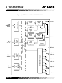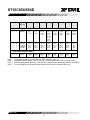
1
EMERALD-MM-8 8-Channel Serial Port PC/104 Module User Manual V2.42 Copyright 2005 DIAMOND SYSTEMS CORPORATION 8430-D Central Ave. Newark, CA 94560 Tel (510) 456-7800 Fax (510) 456-7878 [email protected] www.diamondsystems.com TABLE OF CONTENTS 1. DESCRIPTION..................................................................................................................................... 3 2. FEATURES ........................................................................................................................................... 3 3. EMERALD-MM-8 BOARD DRAWING ........................................................................................... 4 4. I/O HEADER PINOUTS ...................................................................................................................... 5 5. I/O HEADER PIN DEFINITIONS...................................................................................................... 7 6. BOARD CONFIGURATION .............................................................................................................. 8 6.1 6.2 6.3 6.4 6.5 PORT AND INTERRUPT REGISTER ADDRESS SELECTION ................................................................... 8 SERIAL PORT CLOCK FREQUENCY ................................................................................................... 9 INTERRUPT SHARING ....................................................................................................................... 9 SERIAL PROTOCOL SELECTION....................................................................................................... 10 RS-422 / RS-485 CABLE ENDPOINT TERMINATION ....................................................................... 10 7. I/O REGISTER MAP ......................................................................................................................... 11 8. I/O REGISTER DETAIL................................................................................................................... 12 8.1 8.2 8.3 8.4 8.5 8.6 8.7 8.8 8.9 8.10 8.11 9. ADDRESS POINTER / ENABLE REGISTER (BASE ADDRESS + 0, READ/WRITE) ............................... 12 ADDRESS / IRQ DATA REGISTER (BASE ADDRESS + 1, WRITE) .................................................... 12 ADDRESS REGISTER READBACK (BASE ADDRESS + 1, READ)....................................................... 13 DIGITAL I/O DIRECTION REGISTER (BASE ADDRESS + 2, WRITE) ................................................. 13 INTERRUPT STATUS REGISTER (BASE ADDRESS + 2, READ)........................................................... 13 DIGITAL I/O OUTPUT REGISTER (BASE ADDRESS + 3, WRITE)...................................................... 14 DIGITAL INPUT REGISTER (BASE ADDRESS + 3, READ)................................................................. 14 EEPROM COMMAND AND ADDRESS REGISTER (BASE ADDRESS + 4, WRITE) ............................. 15 EEPROM BUSY STATUS (BASE ADDRESS + 4, READ) .................................................................. 15 EEPROM DATA REGISTER (BASE ADDRESS + 5, READ/WRITE) .................................................. 16 CONFIGURATION REGISTER RELOAD COMMAND (BASE ADDRESS + 6, WRITE) ............................ 16 EEPROM OPERATION.................................................................................................................... 17 9.1 EEPROM MAP AND DESCRIPTION ................................................................................................ 17 9.2 HOW TO USE THE EEPROM .......................................................................................................... 18 10. INSTALLING EMERALD-MM-8 IN YOUR SYSTEM ............................................................ 19 11. SPECIFICATIONS......................................................................................................................... 21 12. ST16C654 QUAD UART DATASHEET ...................................................................................... 22 2003 Diamond Systems Corp. Emerald-MM-8 User Manual V2.42 Page 2 EMERALD-MM-8 8-Channel Multi-Protocol Serial Port PC/104 Modules 1. DESCRIPTION Emerald-MM-8 is a PC/104 I/O module with 8 serial ports. Depending on the version, the ports are either fixed in a predetermined protocol or can be jumper configured for multiple protocols: EMM-8M-XT 8 ports jumper configurable for RS-232, RS-422, or RS-485 EMM-8232-XT 8 ports fixed in RS-232 I/O addresses and interrupt levels are programmable for each port, allowing maximum configuration flexibility. For applications where fixed addresses are desirable, four groups of preset addresses are provided that can be selected by jumper settings. Two I/O headers are provided, with four serial ports on each header. The board operates on +5V only, eliminating the need for a +12V supply that is often required for serial port operation. Emerald-MM-8 is based on the 16C654 quad serial port IC. This device contains 4 identical sets of registers, one for each port, and is compatible with the standard PC serial port. The 16C654 has 64-byte FIFOs and operates up to 460.8kbaud. Complete descriptions of these UARTs may be found in the Appendix. Most users will not need this programming information, as it is normally handled by the operating system’s communications software. 2. FEATURES ♦ ♦ ♦ ♦ ♦ ♦ ♦ ♦ ♦ ♦ ♦ 8 serial ports with 64-byte transmit and receive FIFOs Configurable RS-232 / RS-422 / RS-485 (depending on the version) Up to 460.8kbps using 16C654 UART Software selectable I/O addresses and interrupt levels EEPROM storage of configuration data for instant availability on power-up I/O lines are short circuit protected 8 programmable digital I/O lines (1 per port) Dual 40-pin I/O headers, 4 ports per header +5V only operation Extended temperature (-40 to +85oC) operation PC/104 form factor 2003 Diamond Systems Corp. Emerald-MM-8 User Manual V2.42 Page 3 3. EMERALD-MM-8 BOARD DRAWING J1: PC/104 bus 8-bit connector J2: PC/104 bus 16-bit connector J3: I/O header for ports 1 – 4 (2x20 pins) + 4 DIO J4: I/O header for ports 5 – 8 (2x20 pins) + 4 DIO J5 – J8: Protocol configuration jumper blocks, two ports per block J9: Board address, interrupt pulldown resistor, and clock configuration 2003 Diamond Systems Corp. Emerald-MM-8 User Manual V2.42 Page 4 4. I/O HEADER PINOUTS Emerald-MM-8 provides two identical 40-pin headers labeled J3 and J4 for the serial ports. Four ports are contained on each header. Pin numbers are marked on the board to assist with connector orientation. Depending on the model you have, each port may be fixed in a single protocol or configurable for different protocols. The template connector pinouts below are provided to show the pinout for each port in each configuration. The actual pinout of each connector will depend on the model you have and the configuration you have set for each port. RS-232 Configuration: J3 Port 1 Port 2 Port 3 Port 4 DCD 1 RXD 1 TXD 1 DTR 1 GND DCD 2 RXD 2 TXD 2 DTR 2 GND DCD 3 RXD 3 TXD 3 DTR 3 GND DCD 4 RXD 4 TXD 4 DTR 4 GND 1 3 5 7 9 11 13 15 17 19 21 23 25 27 29 31 33 35 37 39 J4 2 4 6 8 10 12 14 16 18 20 22 24 26 28 30 32 34 36 38 40 2003 Diamond Systems Corp. DSR 1 RTS 1 CTS 1 RI 1 DIO A DSR 2 RTS 2 CTS 2 RI 2 DIO B DSR 3 RTS 3 CTS 3 RI 3 DIO C DSR 4 RTS 4 CTS 4 RI 4 DIO D Port 5 Port 6 Port 7 Port 8 DCD 5 RXD 5 TXD 5 DTR 5 GND DCD 6 RXD 6 TXD 6 DTR 6 GND DCD 7 RXD 7 TXD 7 DTR 7 GND DCD 8 RXD 8 TXD 8 DTR 8 GND 1 3 5 7 9 11 13 15 17 19 21 23 25 27 29 31 33 35 37 39 2 4 6 8 10 12 14 16 18 20 22 24 26 28 30 32 34 36 38 40 Emerald-MM-8 User Manual V2.42 DSR 5 RTS 5 CTS 5 RI 5 DIO E DSR 6 RTS 6 CTS 6 RI 6 DIO F DSR 7 RTS 7 CTS 7 RI 7 DIO G DSR 8 RTS 8 CTS 8 RI 8 DIO H Page 5 RS-422 Configuration: J3 Port 1 Port 2 Port 3 Port 4 NC TXD+ 1 GND RXD+ 1 GND NC TXD+ 2 GND RXD+ 2 GND NC TXD+ 3 GND RXD+ 3 GND NC TXD+ 4 GND RXD+ 4 GND 1 3 5 7 9 11 13 15 17 19 21 23 25 27 29 31 33 35 37 39 J4 2 4 6 8 10 12 14 16 18 20 22 24 26 28 30 32 34 36 38 40 NC TXD- 1 RXD- 1 NC DIO A NC TXD- 2 RXD- 2 NC DIO B NC TXD- 3 RXD- 3 NC DIO C NC TXD- 4 RXD- 4 NC DIO D Port 5 Port 6 Port 7 Port 8 NC TXD+ 5 GND RXD+ 5 GND NC TXD+ 6 GND RXD+ 6 GND NC TXD+ 7 GND RXD+ 7 GND NC TXD+ 8 GND RXD+ 8 GND 1 3 5 7 9 11 13 15 17 19 1 3 5 7 9 11 13 15 17 19 2 4 6 8 10 12 14 16 18 20 2 4 6 8 10 12 14 16 18 20 NC TXD- 5 RXD- 5 NC DIO E NC TXD- 6 RXD- 6 NC DIO F NC TXD- 7 RXD- 7 NC DIO G NC TXD- 8 RXD- 8 NC DIO H RS-485 Configuration: J3 Port 1 Port 2 Port 3 Port 4 NC TXD/RXD+ 1 GND NC GND NC TXD/RXD+ 2 GND NC GND NC TXD/RXD+ 3 GND NC GND NC TXD/RXD+ 4 GND NC GND 1 3 5 7 9 11 13 15 17 19 21 23 25 27 29 31 33 35 37 39 2003 Diamond Systems Corp. J4 2 4 6 8 10 12 14 16 18 20 22 24 26 28 30 32 34 36 38 40 NC TXD/RXD- 1 NC NC DIO A NC TXD/RXD- 2 NC NC DIO B NC TXD/RXD- 3 NC NC DIO C NC TXD/RXD- 4 NC NC DIO D Port 5 Port 6 Port 7 Port 8 NC TXD/RXD+ 5 GND NC GND NC TXD/RXD+ 6 GND NC GND NC TXD/RXD+ 7 GND NC GND NC TXD/RXD+ 8 GND NC GND Emerald-MM-8 User Manual V2.42 1 3 5 7 9 11 13 15 17 19 1 3 5 7 9 11 13 15 17 19 2 4 6 8 10 12 14 16 18 20 2 4 6 8 10 12 14 16 18 20 NC TXD/RXD- 5 NC NC DIO E NC TXD/RXD- 6 NC NC DIO F NC TXD/RXD- 7 NC NC DIO G NC TXD/RXD- 8 NC NC DIO H Page 6 5. I/O HEADER PIN DEFINITIONS Signal Name RS-232: DCD DSR RXD RTS TXD CTS DTR RI Definition Direction Data Carrier Detect Data Set Ready Receive Data Request To Send Transmit Data Clear To Send Data Terminal Ready Ring Indicator Input Input Input Output Output Input Output Input RS-422: TXD+, TXDRXD+, RXD- Differential Transmit Data Differential Receive Data Output Input RS-485: TXD/RXD+ TXD/RXD- Differential Transmit/Receive + Differential Transmit/Receive - Bi-directional Bi-directional Common to all protocols: DIO A – H Digital I/O lines GND Ground NC Not Connected 2003 Diamond Systems Corp. Programmable --- Emerald-MM-8 User Manual V2.42 Page 7 6. BOARD CONFIGURATION Refer to the Drawing of Emerald-MM-8 on page 4 for locations of the configuration items mentioned here. 6.1 Port and Interrupt Register Address Selection Each peripheral board in the computer system must have a unique I/O address or block of addresses. Emerald-MM actually uses nine I/O address blocks: one for each of the eight serial ports and one for the board’s configuration registers. Each serial port’s address block consists of 8 consecutive addresses, while the configuration and interrupt status register block occupies four addresses. Jumper block J9 in the lower left corner of the board is used for configuration of the board’s base address. The serial port I/O addresses are set in software once this base address is known. To help with the translation between jumper settings and addresses, remember that each jumper installed corresponds to a 0, and each jumper out corresponds to a 1. The 4 jumpers D C B A correspond to address bits 9 8 7 6, and address bits 5 – 0 are forced to 0 to determine the base address. Only 12 address settings are valid. The four jumper combinations with both D and C in are invalid settings. Board Configuration Register Addresses (Base Address) D C B A Addr. Pointer Register Data Register DIO Direction Register, Interrupt Status Register In Out In In 100 101 102 103 In Out In Out 140 141 142 143 In Out Out In 180 181 182 183 In Out Out Out 1C0 1C1 1C2 1C3 Out In In In 200 201 202 203 Out In In Out 240 241 242 243 Out In Out In 280 281 282 283 Out In Out Out 2C0 2C1 2C2 2C3 Out Out In In 300 301 302 303 Out Out In Out 340 341 342 343 Out Out Out In 380 381 382 383 Out Out Out Out 3C0 3C1 3C2 3C3 2003 Diamond Systems Corp. Emerald-MM-8 User Manual V2.42 DIO Register Page 8 6.2 Serial Port Clock Frequency Serial port boards using the 16C654 UART can operate at higher speeds than the standard 16C554 UART, up to 460.8kbaud vs 115.2kbaud. A 7.3728MHz oscillator is installed on Emerald-MM-8 to enable these higher baud rates. To maintain baud rate compatibility with “standard” 16C554 boards and driver software, the CK jumper in location J9 should be removed. This causes the clock to be divided by 4 to maintain compatibility with software that is expecting a 1.8432MHz clock. To use the higher speed baud rates above 115.2kbaud, the CK jumper should be installed. In “standard” operating system driver software, this setting causes the actual baud rate to be 4x the programmed speed (for example, if you select 115.2kbaud in software, the actual baud rate will be 460.8kbaud). Newer driver software that is capable of directly programming the extended features of the 16C654 UART can control the baud rate in software, so in these configurations the CK jumper setting can be ignored. 6.3 Interrupt Sharing On the PC/104 bus, interrupt levels may be shared by multiple devices. For this reason, the interrupt is driven to a logic high level by the device requesting service, and when the device is serviced it tri-states the line rather than driving it low. This technique avoids contention by two devices trying to drive the line with opposing logic levels. In order to guarantee valid logic levels on the line when the device is not requesting service, each active interrupt level requires a 1KΩ pulldown resistor. Only one such resistor should be used on each active interrupt line. For each interrupt level available on Emerald-MM-8, there is a position on J9 with that interrupt level no. for enabling the pulldown resistor. Install a jumper in this position to connect the resistor, and remove the jumper to disconnect the resistor. 2003 Diamond Systems Corp. Emerald-MM-8 User Manual V2.42 Page 9 6.4 Serial Protocol Selection Jumper blocks J5 through J8 are used to select the protocol for each serial port. Each jumper block configures two ports. Each port may have its protocol set independently of the others. Note that the orientation of jumper blocks J7 and J8 (ports 5 – 8) is rotated 180 degrees from that of J5 and J6 (ports 1 – 4). Configuration drawings are provided below for each group of ports to avoid confusion. Two configurations are shown for RS-422 and RS-485, with and without line termination. 6.5 RS-422 / RS-485 Cable Endpoint Termination In RS-422 or RS-485 networks, termination resistors are normally installed at the endpoints of the cables to minimize reflections on the lines. Emerald-MM-8 provides 120Ω resistors for this purpose. To enable resistor termination for a port, install jumpers in the locations T and R of that port’s corresponding configuration jumper block as shown on the previous page. Termination is only needed, and should only be used, at the cable endpoints. Enabling these termination resistors at each end of the cable results in an effective impedance of 60Ω. Installing termination resistors at additional points in the network may cause overloading and failure of the line drivers due to the lower impedance caused by multiple resistors in parallel. 2003 Diamond Systems Corp. Emerald-MM-8 User Manual V2.42 Page 10 7. I/O REGISTER MAP Emerald-MM-8 Register Map Base Address + 0 1 2 3 4 5 6 7 Write Address pointer / enable register Data for address / IRQ no. Digital I/O direction register Digital output register EEPROM read/write + address EEPROM data (write operation) Reload command N/A Read Address pointer / enable register Readback of address registers Interrupt status register Digital input / readback register EEPROM busy status EEPROM data (read operation) N/A N/A Emerald-MM-8 contains 16 additional registers for selecting the address and interrupt level for each port. These registers are accessed through the address pointer register at Base + 0. The register map is shown below: Register No. 0 1 2 3 4 5 6 7 8 9 10 11 12 13 14 15 Function Port 0 Address Port 1 Address Port 2 Address Port 3 Address Port 4 Address Port 5 Address Port 6 Address Port 7 Address Port 0 IRQ No. Port 1 IRQ No. Port 2 IRQ No. Port 3 IRQ No. Port 4 IRQ No. Port 5 IRQ No. Port 6 IRQ No. Port 7 IRQ No. To write data to a register, first write the number of that register (0 – 15) to the board’s address pointer / enable register at Base address + 0. Then write the data to the board’s data register at Base address + 1. To program an address for a port, write the upper 7 bits of the 10 bit I/O address into bits 6 – 0 of the address register for that port. The value written to the address register is therefore the desired I/O address divided by 8. All I/O addresses should be on 8 byte boundaries between 100 Hex and 3F8 Hex. Addresses below 100 Hex are reserved for CPU functions. To select an interrupt level for a port, write the desired interrupt level to that port’s interrupt level register. Valid interrupt levels are 2, 3, 4, 5, 6, 7, 10, 11, 12, and 15. Writing any other value to the interrupt level register will cause that port not to generate interrupts. Bit 7 of Base address + 0 is the port enable bit and must be set after manual loading of port addresses and interrupts in order to enable serial port operation. On power-up or reset, all ports are automatically reloaded with the EEPROM values and then enabled. 2003 Diamond Systems Corp. Emerald-MM-8 User Manual V2.42 Page 11 8. I/O REGISTER DETAIL 8.1 Address Pointer / Enable Register (Base Address + 0, Read/Write) This register selects the address or IRQ register to be programmed and also enables the serial ports. The value written to this register can be read back for diagnostic purposes. After writing the address to this register, the appropriate data is written to the data register at Base address + 1. See 8.2 below. Bit No. 7 6 5 4 3 2 1 0 Name ENABLE X X X A3 A2 A1 A0 ENABLE Enables chip selects for the 8 serial ports. 1 = enable, 0 = disable On power-up or reset, all ports are automatically programmed from the EEPROM and enabled. When manually programming the address and IRQ registers, this bit must be set after programming is complete in order to enable the serial ports. X Not used A3 – 0 Address of internal configuration register: 0 – 7 Address registers for ports 0 – 7 respectively 8 – 15 Interrupt level register for ports 0 – 7 respectively 8.2 Address / IRQ Data Register (Base Address + 1, Write) This register is used to write data to the register selected with the address / enable register described above. The data must be written to this register after the address is selected. Note that writing to the board’s serial port address and IRQ registers does not cause a writethrough to the corresponding EEPROM registers. The user must explicitly write the data to the EEPROM to store these settings for future use when the board is reset or the power is cycled. Bit No. 7 6 5 4 3 2 1 0 Name X D6 D5 D4 D3 D2 D1 D0 X Not used D6 – 0 Register data; For address registers, D6 – 0 contains the upper 7 bits of the 10-bit base address of the serial port. Valid port base addresses are 100 Hex to 3F8 Hex. For interrupt level registers, Only D3 – 0 are used. Valid values are 2, 3, 4, 5, 6, 7, 10, 11, 12, and 15. Any other value will prevent interrupts from operating on the selected port. I/O Address example Desired I/O address = 140 Hex = 0 1 0 1 0 0 0 0 0 0 Only the upper 7 bits are needed. The three lowest bits are always 0, resulting in all addresses being on 8-byte boundaries. Necessary bits = 0 1 0 1 0 0 0 = 28 Hex An easy way to generate these bits is to divide the I/O address by 8 or shift right 3 places. 2003 Diamond Systems Corp. Emerald-MM-8 User Manual V2.42 Page 12 8.3 Address Register Readback (Base Address + 1, Read) This register provides a means to read back the current address settings for Ports 1 – 8 as a diagnostic tool to verify that the board is present and responding. Using this technique, all 8 address registers can be read back, but the IRQ registers cannot be read back. All 16 register values can be read back from the EEPROM; see page 15 for details. 8.4 Digital I/O Direction Register (Base Address + 2, Write) This register determines the direction of each of the 8 digital I/O lines. The direction of each bit can be programmed individually. This register is cleared to 0 on reset or power-up (all bits in input mode). Bit No. 7 6 5 4 3 2 1 0 Name DIR 7 DIR 6 DIR 5 DIR 4 DIR 3 DIR 2 DIR 1 DIR 0 Dir 7 – 0 0 = input, 1 = output 8.5 Interrupt Status Register (Base Address + 2, Read) The interrupt status register indicates the status of each port’s interrupt request line. It operates regardless of whether interrupt sharing is enabled (see below). If two or more ports are sharing the same interrupt level, the status register will still indicate the correct status of each port’s interrupt request line. If different ports are sharing different interrupt levels, the status register will still operate properly. Bit No. 7 6 5 4 3 2 1 0 Name INT 7 INT 6 INT 5 INT 4 INT 3 INT 2 INT 1 INT 0 Definitions: INT 7 – 0 Status of interrupt request for each port: 0 = no interrupt request active 1 = interrupt request active 2003 Diamond Systems Corp. Emerald-MM-8 User Manual V2.42 Page 13 8.6 Digital I/O Output Register (Base Address + 3, Write) This register programs the digital output lines on the I/O headers. Any line set to output mode using the configuration register at base + 2 will be set to the value specified in this register. Any I/O line in input mode will not be affected. The digital output register is cleared to 0 on power up or system reset. Bit No. 7 6 5 4 3 2 1 0 Name Dout 7 Dout 6 Dout 5 Dout 4 Dout 3 Dout 2 Dout 1 Dout 0 Dout 7 – 0 Set digital output line to value specified 8.7 Digital Input Register (Base Address + 3, Read) This register returns the state of the 8 digital I/O lines on the I/O headers. Any line in output mode will be read back. Any line in input mode will be read as the state of the pin on the I/O header. Input pins that are not driven externally will float. They will have an unpredictable readback value, and the value may change on successive read operations. This is normal behavior for a floating input pin. Bit No. 7 6 5 4 3 2 1 0 Name DIO 7 DIO 6 DIO 5 DIO 4 DIO 3 DIO 2 DIO 1 DIO 0 DIO 7 – 0 Logic state of I/O line 7 - 0 2003 Diamond Systems Corp. Emerald-MM-8 User Manual V2.42 Page 14 8.8 EEPROM Command and Address Register (Base Address + 4, Write) This register is used to initiate an EEPROM read or write operation. First the data is written to Base + 5, then the address and read/write bit are written to this register to initiate the operation. After writing the operation has started, the application program should monitor the Busy bit by reading this address to know when the operation is complete. Bit No. 7 6 5 4 3 2 1 0 Name R/W EEA6 EEA5 EEA4 EEA3 EEA2 EEA1 EEA0 R/W Read/Write bit: 1 = write operation, 0 = read operation EEA6-0 EEPROM address; The EEPROM has 256 bytes; only the lowest 64 are accessible. Only the lowest 16 contain configuration information for the board. The other registers are available for customer application. 8.9 EEPROM Busy Status (Base Address + 4, Read) The Busy bit indicates whether the EEPROM is busy with a read, write, or reload operation. The application program must monitor this bit after each read, write, or reload operation before proceeding to another one. If a new EEPROM operation is commenced without waiting for the previous one to finish, the new operation will be ignored. Bit No. 7 6 5 4 3 2 1 0 Name BUSY X X X X X X X BUSY EEPROM Busy status: 1 = busy, 0 = idle X Not used 2003 Diamond Systems Corp. Emerald-MM-8 User Manual V2.42 Page 15 8.10 EEPROM Data Register (Base Address + 5, Read/Write) When writing to the EEPROM, the data is first written to this register before the address and write bit are written to Base + 4. When reading from the EEPROM, the address to read from is first written to Base + 4. Then the program must monitor the BUSY bit in Base + 4. When it is 0, the program may read the EEPROM data from this register. Bit No. 7 6 5 4 3 2 1 0 Name EED7 EED6 EED5 EED4 EED3 EED2 EED1 EED0 EED7 – 0 EEPROM data 8.11 Configuration Register Reload Command (Base Address + 6, Write) This register is used to cause a reload of the contents of the EEPROM into the board’s configuration registers. This can be done at any time, for example to recall known good settings in case the user loads invalid data into the registers. Bit No. 7 6 5 4 3 2 1 0 Name RELOAD X X X X X X X RELOAD Set to 1 to force a reload of the 8 address settings and 8 interrupt level settings from the EEPROM into the board. The BUSY bit (Base + 4 bit 7) will go high and stay high until the reload is complete. X Not used 2003 Diamond Systems Corp. Emerald-MM-8 User Manual V2.42 Page 16 9. EEPROM OPERATION 9.1 EEPROM Map and Description Emerald-MM-8 V2.1 has an EEPROM for storage of the address and interrupt level settings for each serial port. The EEPROM has 256 bytes total, of which the lowest 128 are addressable. Only the lowest 16 registers in the EEPROM are used. The first 8 locations (07) are used to store the base address values for the 8 serial ports. The second 8 locations (815) are for the 8 interrupt levels (IRQ numbers). The memory map of the EEPROM is identical to the register map for the addresses and interrupts on Emerald-MM-8: EEPROM Address 0 1 2 3 4 5 6 7 8 9 10 11 12 13 14 15 Function Port 0 Address Port 1 Address Port 2 Address Port 3 Address Port 4 Address Port 5 Address Port 6 Address Port 7 Address Port 0 IRQ No. Port 1 IRQ No. Port 2 IRQ No. Port 3 IRQ No. Port 4 IRQ No. Port 5 IRQ No. Port 6 IRQ No. Port 7 IRQ No. The address values stored in EEPROM are the upper 7 bits of the 10-bit serial port address. Each serial port uses 8 registers, so the binary base address of each serial port always ends in 000. To determine the value to store in the EEPROM, divide the desired base address by 8: Desired base address = 120 Hex = 0 1 0 0 1 0 0 0 0 0 = 288 Decimal EEPROM value = 288 / 8 = 36 Decimal = 24 Hex = 0 1 0 0 1 0 0 These are the 7 uppermost bits of the original base address. This value would be written to the selected port’s address location in the EEPROM to program that port for The IRQ numbers stored in EEPROM are the actual IRQ numbers without any changes. Each port may be programmed for its own IRQ number, or any number of ports may share an IRQ. Not all IRQs are available in all computers. You will need to test for availability and operability of the selected IRQ. NOTE: The serial port base addresses must be distinct from each other and must also be distinct from the board’s base address. If any serial port’s address is programmed to overlap with the board’s base address, that port will not be accessible, and the address will have to be reconfigured. 2003 Diamond Systems Corp. Emerald-MM-8 User Manual V2.42 Page 17 9.2 How to Use the EEPROM There are three available EEPROM operations: write data, read data, and reload data. The write and read operations store data in the EEPROM but have no effect on the board’s configuration settings. The reload operation updates the board’s configuration settings to match the configuration values stored in the EEPROM. Note that writing to the board’s serial port address and IRQ registers does not cause a writethrough to the corresponding EEPROM registers. The user must explicitly write the data to the EEPROM to store these settings for future use when the board is reset or the power is cycled. The EEPROM contains 256 bytes. However only locations 0 – 127 may be accessed, since the address is limited to 7 bits. Only EEPROM addresses 0 – 15 are used to store configuration data for Emerald-MM-8. The remaining locations from 16 and up are available for customer application use. EPROM Write Operation: 1. Write data to Base + 5 2. Write 7-bit address including Write bit (bit 7 = 1) to Base + 4 3. Monitor Busy bit (bit 7) in base + 4 until it is 0 EEPROM Read Operation: 1. Write 7-bit address to Base + 4 (Bit 7 = 0 for read) 2. Monitor Busy bit (bit 7) in base + 4 until it is 0 3. Read data from Base + 5 EEPROM Reload Operation: 1. Write 0x80 (128) to Base + 6 to initiate Reload operation 2. Monitor Busy bit (bit 7) in base + 4 until it is 0 2003 Diamond Systems Corp. Emerald-MM-8 User Manual V2.42 Page 18 10. INSTALLING EMERALD-MM-8 IN YOUR SYSTEM Diamond Systems provides utility programs to configure the Emerald-MM-8 board for use in your computer system. For DOS and Windows 9x applications, the program will configure the address and interrupt settings, store them in the EEPROM on the board, and allow you to store them in a file which can be used later to program additional boards with the same configuration. For Windows NT applications, the program will additionally configure the NT registry with the proper settings according to the configuration you select. The configuration programs and instructions are in the zip file EMM8.zip that is included in the board’s software diskette. For DOS and Windows 9x applications, complete instructions are in the file readme.txt in the DOS-9x folder, and the application program is called eepconf.exe. For Windows NT applications, complete instructions are in the file EMM8-NT.txt in the NT folder, and the application is called Emm8Conf.exe. The instructions below may be used to manually set up Windows NT to run with the board. However these instructions are not needed if Emm8Conf.exe is used. 1. Run REGEDT32.EXE and go to the following dialog box: Key_Local_Machine \ System \ CurrentControlSet \ Service \ Serial \ Parameters 2. Add a new key for each serial port by selecting Edit \ Add Key. The following parameters need to be specified for each serial port: SerialN (N = serial port number, 1, 2, 3, 4, etc.): Parameter DosDevices ForceFifoEnable Interrupt Type REG_SZ REG_DWORD REG_DWORD InterruptStatus REG_DWORD PortAddress PortIndex REG_DWORD REG_DWORD SharedInterrupts REG_DWORD Value, Comments Name of port, e.g. COM5, COM6 0x1 for yes IRQ level in Hex format, e.g. 0x5 for 5 or 0xA for 10 Address of interrupt status register in Hex, e.g. 0x102; See page 8 for status register addresses Address or port in Hex, e.g. 0x120 for Hex 120 Bit position in status register: 0x1 for LSB through 0x8 for MSB (Note this is NOT the weighted bit value); See page 13 for details 0x1 for yes, 0x0 for no 3. Exit REGEDT32.EXE and restart NT. See the example parameter values on the following page. 2003 Diamond Systems Corp. Emerald-MM-8 User Manual V2.42 Page 19 Windows NT Registry Setup Example The following example is for 8 ports on an EMM-8M-XT board installed on a CPU that already contains 2 serial ports called COM1 and COM2. Note that all 8 ports on the EmeraldMM-8 board share the same interrupt status register, but the bit position changes for each port. The settings shown are the factory settings for the board. All ports are set to share the same interrupt number. Configuration selections: Port 1 0x100 7 Port 2 0x108 7 Board base address: Interrupt status register: 0x200 0x202 Address IRQ No. Serial3: DosDevices ForceFifoEnable Interrupt InterruptStatus PortAddress PortIndex SharedInterrupts Serial4: DosDevices ForceFifoEnable Interrupt InterruptStatus PortAddress PortIndex SharedInterrupts Serial5: DosDevices ForceFifoEnable Interrupt InterruptStatus PortAddress PortIndex SharedInterrupts Serial6: DosDevices ForceFifoEnable Interrupt InterruptStatus PortAddress PortIndex SharedInterrupts REG_SZ COM3 REG_DWORD REG_DWORD REG_DWORD REG_DWORD REG_DWORD REG_DWORD REG_SZ COM4 REG_DWORD REG_DWORD REG_DWORD REG_DWORD REG_DWORD REG_DWORD REG_SZ COM5 REG_DWORD REG_DWORD REG_DWORD REG_DWORD REG_DWORD REG_DWORD REG_SZ COM6 REG_DWORD REG_DWORD REG_DWORD REG_DWORD REG_DWORD REG_DWORD 2003 Diamond Systems Corp. Port 3 0x110 7 Port 4 0x118 7 Port 5 0x120 7 Port 6 0x128 7 Serial7: DosDevices 0x1 0x7 0x202 0x100 0x1 0x1 0x1 0x7 0x202 0x120 0x5 0x1 REG_SZ COM8 REG_DWORD REG_DWORD REG_DWORD REG_DWORD REG_DWORD REG_DWORD 0x1 0x7 0x202 0x128 0x6 0x1 ForceFifoEnable Interrupt InterruptStatus PortAddress PortIndex SharedInterrupts REG_SZ COM9 REG_DWORD REG_DWORD REG_DWORD REG_DWORD REG_DWORD REG_DWORD 0x1 0x7 0x202 0x130 0x7 0x1 Serial10: DosDevices ForceFifoEnable Interrupt InterruptStatus PortAddress PortIndex SharedInterrupts REG_SZ COM10 REG_DWORD 0x1 REG_DWORD 0x7 REG_DWORD 0x202 REG_DWORD 0x138 REG_DWORD 0x8 REG_DWORD 0x1 ForceFifoEnable Interrupt InterruptStatus PortAddress PortIndex SharedInterrupts ForceFifoEnable Interrupt InterruptStatus PortAddress PortIndex SharedInterrupts Serial9: DosDevices 0x1 0x7 0x202 0x110 0x3 0x1 0x1 0x7 0x202 0x118 0x4 0x1 Port 8 0x138 7 REG_SZ COM7 REG_DWORD REG_DWORD REG_DWORD REG_DWORD REG_DWORD REG_DWORD Serial8: DosDevices 0x1 0x7 0x202 0x108 0x2 0x1 Port 7 0x130 7 Emerald-MM-8 User Manual V2.42 Page 20 11. SPECIFICATIONS Serial Ports No. of serial ports: 8 Protocols: EMM-8M-XT: RS-232, RS-422, RS-485 EMM-8232-XT: RS-232 460.8kbaud 5, 6, 7, or 8 data bits; Even, odd, or no parity All outputs protected against continuous short circuit Maximum baud rate: Communications parameters: Short circuit protection: RS-232 mode: (Models EMM-8M-XT, EMM-8232-XT) Input impedance: 3KΩ min Input voltage swing: ±30V max Output voltage swing: ±5V min, ±7V typical RS-422, RS-485 modes: Differential input threshold: (Model EMM-8M-XT) -0.2V min, +0.2V max Input impedance: Input current: 12KΩ min +1.0mA max (VIN = 12V) -0.8mA max (VIN = -7V) Differential output voltage: High/low states differential output voltage symmetry: 2.0V min (RL = 50Ω) Digital I/O 0.2V max (At VCC = 5.0VDC) No. of I/O lines: Input voltage: 8, programmable direction Low: -0.3V min, 0.8V max High: 2.0V min, 5.3V max Output voltage: Low: 0.0V min, 0.4V max (IOL = 6mA max) High: 3.7V min, 5.0V max (IOH = -4mA max) General I/O header: Dimensions: Power supply: Current consumption: Operating temperature: Operating humidity: PC/104 bus: 2003 Diamond Systems Corp. 2 40-position (2x20) .025” square pin header on .1” centers; Headers mate with standard ribbon cable (IDC) connectors 3.55” x 3.775” LxW (PC/104 standard) +5VDC ±10% 160mA typical, all outputs unloaded -40 to +85oC (Industrial range) 5% to 95% noncondensing 8 bit and 16-bit bus headers are installed and used (16-bit header is used for interrupt levels only) Emerald-MM-8 User Manual V2.42 Page 21 ST16C654/654D QUAD UART WITH 64-BYTE FIFO AND INFRARED (IrDA) ENCODER/DECODER DESCRIPTION The ST16C654 *1 is a universal asynchronous receiver and transmitter (UART) with a dual foot print interface compatible with the ST16C554 and ST68C554. The 654 is an enhanced UART with 64 byte FIFOs, automatic hardware/software flow control, and data rates up to 1.5Mbps. Onboard status registers provide the user with error indications and operational status, modem interface control. System interrupts may be tailored to meet user requirements. An internal loop-back capability allows onboard diagnostics. The 654 is available in 64 pin TQFP, 68 pin PLCC, and 100 pin QFP packages. The 64 pin package offers the 16 interface mode which is compatible with the industry standard ST16C554. The 68 and 100 pin packages offer an additional 68 mode which allows easy integration with Motorola, and other popular microprocessors. The ST16C654CQ64 (64 pin) offers three state interrupt control while the ST16C654DCQ64 provides constant active interrupt outputs. The 64 pin devices do not offer TXRDY/RXRDY outputs or the default clock select option (CLKSEL). The 100 pin packages offer faster channel status access by providing separate outputs for TXRDY and RXRDY, offer separate Infrared TX outputs and a musical instrument clock input (MIDICLK). The 654 combines the package interface modes of the 16C454/ 554 and 68/C454/554 series on a single integrated chip. FEATURES Part number ST16C654CJ68 ST16C654CQ64 ST16C654DCQ64 ST16C654CQ100 Pins 68 64 64 100 Package Operating temperature PLCC TQFP TQFP QFP 0° C to + 70° C 0° C to + 70° C 0° C to + 70° C 0° C to + 70° C -CDA -RIA RXA GND D7 D6 D5 D4 D3 D2 D1 D0 INTSEL VCC RXD -RID -CDD 9 8 7 6 5 4 3 2 1 68 67 66 65 64 63 62 63 -DSRA 10 60 -DSRD -CTSA 11 59 -CTSD -DTRA 12 58 -DTRD VCC 13 57 GND -RTSA 14 56 -RTSD INTA 15 55 INTD -CSA 16 54 -CSD TXA 17 53 TXD -IOW 18 52 -IOR TXB 19 51 TXC -CSB 20 50 -CSC INTB 21 49 INTC -RTSB 22 48 -RTSC GND 23 47 VCC -DTRB 24 46 -DTRC -CTSB 25 45 -CTSC -DSRB 26 44 -DSRC 40 41 42 43 RXC -RIC -CDC 39 -TXRDY GND 38 34 A0 -RXRDY 33 A1 37 32 A2 RESET 31 16/-68 36 30 CLKSEL Pins 68 64 64 100 XTAL2 29 RXB ST16C654IJ68 ST16C654IQ64 ST16C654DIQ64 ST16C654IQ100 35 28 Part number XTAL1 27 ST16C654CJ68 16 MODE -RIB ORDERING INFORMATION PLCC Package -CDB • Compatibility with the Industry Standard ST16C454/554, ST68C454/554, TL16C554 • 1.5 Mbps transmit/receive operation (24MHz) • 64 byte transmit FIFO • 64 byte receive FIFO with error flags • Automatic software/hardware flow control • Programmable Xon/Xoff characters • Independent transmit and receive control • Software selectable Baud Rate Generator prescaleable clock rates of 1X, 4X. • Four selectable Transmit/Receive FIFO interrupt trigger levels • Standard modem interface or infrared IrDA encoder/decoder interface • Software flow control turned off optionally by any (Xon) RX character • Independent MIDI interface on 100 pin packages • 100 pin packages offer internal register FIFO monitoring and separate IrDA TX outputs • Sleep mode ( 200mA stand-by) Package Operating temperature PLCC TQFP TQFP QFP -40° C to + 85° C -40° C to + 85° C -40° C to + 85° C -40° C to + 85° C Note *1: Patent Pending Rev. 4.30 EXAR Corporation, 48720 Kato Road, Fremont, CA 94538 • (510) 668-7000 • FAX (510) 668-7017 ST16C654/654D Figure 1, Package Descriptions 35 VCC -DTRB 15 34 -DTRC -CTSB 16 33 -CTSC 21 22 23 24 25 26 27 28 29 30 31 VCC A2 A1 A0 XTAL1 XTAL2 RESET GND RXC -RIC -CDC D7 D6 D5 D4 D3 D2 D1 D0 N.C. VCC RXD -RID -CDD 4 3 2 1 68 67 66 65 64 63 62 61 48 -RTSC GND 23 47 VCC -DTRB 24 46 -DTRC -CTSB 25 45 -CTSC -DSRB 26 44 -DSRC 32 20 RXB 22 -DSRC 19 -RIB N.C. -RTSB N.C. 18 49 N.C. 17 21 -DSRA -CDB A4 N.C. -CTSA -DSRB 50 43 14 20 -CDC GND TXC A3 42 -RTSC 51 -RIC 36 19 41 13 N.C. TXB RXC -RTSB 52 ST16C654CJ68 68 MODE 40 INTC 18 GND 37 TXD R/-W 39 12 53 -TXRDY INTB 17 38 -CSC N.C. TXA -RXRDY 38 54 37 11 16 -RESET -CSB N.C. -CS 36 TXC 55 XTAL2 39 15 35 10 -RTSD -IRQ XTAL1 -TXB 56 34 -IOR 14 A0 40 ST16C654DCQ64 GND -RTSA 33 9 57 A1 -IOW ST16C654CQ64 13 32 TXA TXD -DTRD VCC A2 -CSD 41 GND -CDD 42 8 5 -RID 49 7 58 31 RXD 50 -CSA 12 16/-68 VCC 51 INTD RXA D0 52 -RTSD 43 6 D1 53 44 6 -CTSD -DTRA 30 D2 54 5 INTA -DSRD 59 CLKSEL D3 55 -RTSA -RIA D4 56 GND 7 D5 57 -DTRD 45 60 11 29 D6 58 46 4 -CDA D7 59 3 VCC 8 GND 60 -DTRA 10 -CTSA RXB -CTSD 9 RXA 61 47 -DSRA 28 -RIA 62 2 -DSRD 27 -CDA 63 48 -RIB -CTSA 1 -CDB -DSRA 68 Pin PLCC Package 64 64 Pin TQFP Package 100 Pin QFP Package N.C. N.C. N.C. N.C. N.C. -TXRDYB IRTXB -DSRB -CTSB -DTRB GND -RTSB INTB -CSB TXB -IOW TXA -CSA INTA -RTSA VCC -DTRA IRTXA -TXRDYA N.C. N.C. 30 29 28 27 26 25 24 23 22 21 20 19 18 17 16 15 14 13 12 11 10 9 8 7 6 5 4 3 2 1 -RXRDYB 31 100 -RXRDYA -CDB 32 99 -CDA -RIB 33 98 -RIA RXB 34 97 RXA CLKSEL 35 96 GND 16/-68 36 95 D7 A2 37 94 D6 A1 38 93 D5 A0 39 92 D4 XTAL1 40 91 D3 XTAL2 41 90 D2 MIDICLK 42 89 D1 RESET 43 88 D0 -RXRDY 44 87 INTSEL -TXRDY 45 86 VCC GND 46 85 RXD RXC 47 84 -RID -RIC 48 83 -CDD -CDC 49 82 -RXRDYD -RXRDYC 50 81 -TXRDYD ST16C654CQ100 51 52 53 54 55 56 57 58 59 60 61 62 63 64 65 66 67 68 69 70 71 72 73 74 75 76 77 78 79 80 N.C. N.C. N.C. N.C. N.C. -TXRDYC IRTXC -DSRC -CTSC -DTRC VCC -RTSC INTC -CSC TXC -IOR TXD -CSD INTD -RTSD GND -DTRD -CTSD -DSRD IRTXD -CSRDY N.C. N.C. N.C. N.C. Rev. 4.30 2 ST16C654/654D Figure 2, Block Diagram 16 Mode XTAL1 MIDI XTAL2 Data bus & Control Logic Register Select Logic Receive FIFO Registers Inter Connect Bus Lines & Control signals INT A-D -RXRDY -TXRDY -RXRDY A-D -TXRDY A-D INTSEL Interrupt Control Logic A0-A2 -CS A-D Flow Control Logic Flow Control Logic Transmit Shift Register TX A-D Ir Encoder Receive Shift Register RX A-D RXIR A-D Ir Decoder -DTR A-D -RTS A-D Modem Control Logic Clock & Baud Rate Generator D0-D7 -IOR -IOW RESET Transmit FIFO Registers Rev. 4.30 3 -CTS A-D -RI A-D -CD A-D -DSR A-D ST16C654/654D SYMBOL DESCRIPTION Symbol 68 Pin 100 64 Signal type 16/-68 31 36 - I 16/68 Interface Type Select (input with internal pull-up). This input provides the 16 (Intel) or 68 (Motorola) bus interface type select. The functions of -IOR, -IOW, INT AD, and -CS A-D are re-assigned with the logical state of this pin. When this pin is a logic 1, the 16 mode interface 16C554 is selected. When this pin is a logic 0, the 68 mode interface (68C554) is selected. When this pin is a logic 0, -IOW is reassigned to R/-W, RESET is re-assigned to -RESET, -IOR is not used, and INT A-D(s) are connected in a WIRE-OR configuration. The WIRE-OR outputs are connected internally to the open source IRQ signal output. This pin is not available on 64 pin packages which operate in the 16 mode only. A0 34 39 24 I Address-0 Select Bit. Internal registers address selection in 16 and 68 modes. A1 33 38 23 I Address-1 Select Bit. Internal registers address selection in 16 and 68 modes. A2 32 37 22 I Address-2 Select Bit. - Internal registers address selection in 16 and 68 modes. 20,50 17,64 - I Address 3-4 Select Bits. - When the 68 mode is selected, these pins are used to address or select individual UARTs (providing -CS is a logic 0). In the 16 mode, these pins are reassigned as chip selects, see -CSB and -CSC. These pins are not available on 64 pin packages which operate in the 16 mode only. CLKSEL 30 35 - I Clock Select. - The 1X or 4X pre-scaleable clock is selected by this pin. The 1X clock is selected when CLKSEL is a logic 1 (connected to VCC) or the 4X is selected when CLKSEL is a logic 0 (connected to GND). MCR bit-7 can override the state of this pin following reset or initialization (see MCR bit7). This pin is not available on 64 pin packages which provide MCR bit-7 selection only. -CS 16 13 - I Chip Select. (active low) - In the 68 mode, this pin functions as a multiple channel chip enable. In this case, all four A3-A4 Pin Description Rev. 4.30 5 ST16C654/654D SYMBOL DESCRIPTION Symbol 68 Pin 100 64 Signal type Pin Description UARTs (A-D) are enabled when the -CS pin is a logic 0. An individual UART channel is selected by the data contents of address bits A3-A4. When the 16 mode is selected (68/100 pin devices), this pin functions as -CSA, see definition under -CS A-B. This pin is not available on 64 pin packages which operate in the 16 mode only. -CS A-B -CS C-D 16,20 50,54 13,17 64,68 7,11 38,42 I Chip Select A, B, C, D (active low) - This function is associated with the 16 mode only, and for individual channels, A through D. When in 16 Mode, these pins enable data transfers between the user CPU and the ST16C654 for the channel(s) addressed. Individual UART sections (A, B, C, D) are addressed by providing a logic 0 on the respective -CS A-D pin. When the 68 mode is selected, the functions of these pins are reassigned. 68 mode functions are described under the their respective name/pin headings. -CSRDY - 76 - I Control Status Ready (active low) - This feature is available on 100 pin QFP packages only. On 100 pin packages, the Contents of the FIFORDY Register is read when this pin is a logic 0. However it should be noted, D0-D3 will contain the inverted logic states of TXRDY, status bits A-D, and D4-D7 the inverted logic states of RXRDY, status bits D4-D7. D0-D2 D3-D7 66-68 1-5 88-90 91-95 53-55 56-60 I/O GND GND 6,23 40,57 96,20 46,71 14,28 45,61 Pwr INT A-B INT C-D 15,21 49,55 12,18 63,69 6,12 37,43 O Data Bus (Bi-directional) - These pins are the eight bit, three state data bus for transferring information to or from the controlling CPU. D0 is the least significant bit and the first data bit in a transmit or receive serial data stream. Signal and power ground. Interrupt A, B, C, D (active high) - This function is associated with the 16 mode only. These pins provide individual channel interrupts, INT A-D. INT A-D are enabled when MCR bit-3 is set to a logic 1, interrupts are enabled in the interrupt enable register (IER), and when an interrupt con- Rev. 4.30 6 ST16C654/654D SYMBOL DESCRIPTION Symbol 68 Pin 100 64 Signal type Pin Description dition exists. Interrupt conditions include: receiver errors, available receiver buffer data, transmit buffer empty, or when a modem status flag is detected. When the 68 mode is selected, the functions of these pins are reassigned. 68 mode functions are described under the their respective name/pin headings. INTSEL 65 87 - I Interrupt Select. (active high, with internal pull-down) - This function is associated with the 16 mode only. When the 16 mode is selected, this pin can be used in conjunction with MCR bit-3 to enable or disable the three state interrupts, INT A-D or override MCR bit-3 and force continuous interrupts. Interrupt outputs are enabled continuously by making this pin a logic 1. Making this pin a logic 0 allows MCR bit-3 to control the three state interrupt output. In this mode, MCR bit-3 is set to a logic 1 to enable the three state outputs. This pin is disabled in the 68 mode. Due to pin limitations on 64 pin packages, this pin is not available. To cover this limitation, two 64 pin QFP package versions are offered. The ST16C654DCQ64 operates in the continuos interrupt enable mode by bonded this pin to VCC internally. The ST16C654CQ64 operates with MCR bit-3 control by bonding this pin to GND. -IOR 52 66 40 I Input/Output Read. (active low Strobe) - This function is associated with the 16 mode only. A logic 0 transition on this pin will load the contents of an Internal register defined by address bits A0-A2 onto the ST16C654 data bus (D0-D7) for access by an external CPU. This pin is disabled in the 68 mode. -IOW 18 15 9 I Input/Output Write. (active low strobe) - This function is associated with the 16 mode only. A logic 0 transition on this pin will transfer the contents of the data bus (D0-D7) from the external CPU to an internal register that is defined by address bits A0/A2. When the 16 mode is selected (68/100 pin devices), this pin functions as R/-W, see definition under R/W. Rev. 4.30 7 ST16C654/654D SYMBOL DESCRIPTION Symbol 68 Pin 100 64 Signal type 15 12 - O Interrupt Request or Interrupt A - This function is associated with the 68 mode only. In the 68 mode, interrupts from UART channels A-D are WIRE-ORed internally to function as a single IRQ interrupt. This pin transitions to a logic 0 (if enabled by the interrupt enable register) whenever a UART channel(s) requires service. Individual channel interrupt status can be determined by addressing each channel through its associated internal register, using -CS and A3A4. In the 68 mode an external pull-up resistor must be connected between this pin and Vcc. The function of this pin changes to INTA when operating in the 16 mode, see definition under INTA. IRTX A-B IRTX C-D - 6,24 57,75 - O Infrared Transmit Data Output (IrDA) - This function is associated with 100 pin packages only. These pins provide separate infrared IrDA TX outputs for UART channels (AD). The serial infrared IRTX data is transmitted via these pins with added start, stop and parity bits. The IRTX signal will be a logic 0 during reset, idle (no data), or when the transmitter is disabled. MCR bit-6 selects the standard modem or infrared interface. MIDICLK - 42 - I MIDI (Musical Instrument Digital Interface) Clock Input This function is associated with 100 pin packages only. RXC and TXC can function as MIDI input/output ports when an external MIDI Clock is provided at this pin. External Clock or a crystal is connected to the XTAL2 pins for normal operation (see XTAL 1 & 2). -RESET RESET 37 43 27 I Reset. - In the 16 mode a logic 1 on this pin will reset the internal registers and all the outputs. The UART transmitter output and the receiver input will be disabled during reset time. (See ST16C654 External Reset Conditions for initialization details.) When 16/-68 is a logic 0 (68 mode), this pin functions similarly but, as an inverted reset interface signal, -RESET. R/-W 18 15 - I Read/Write Strobe (active low) - This function is associated -IRQ Pin Description Rev. 4.30 8 ST16C654/654D SYMBOL DESCRIPTION Symbol 68 Pin 100 64 Signal type Pin Description with the 68 mode only. This pin provides the combined functions for Read or Write strobes. A logic 1 to 0 transition transfers the contents of the CPU data bus (D0-D7) to the register selected by -CS and A0-A4. Similarly a logic 0 to 1 transition places the contents of a 654 register selected by -CS and A0-A4 on the data bus, D0-D7, for transfer to an external CPU. -RXRDY -RXRDY A-B -RXRDY C-D -TXRDY 38 44 - O Receive Ready (active low) - This function is associated with 68 and 100 pin packages only. -RXRDY contains the wire OR-ed status of all four receive channel FIFOs, RXRDY A-D. A logic 0 indicates receive data ready status, i.e. the RHR is full or the FIFO has one or more RX characters available for unloading. This pin goes to a logic 1 when the FIFO/RHR is full or when there are no more characters available in either the FIFO or RHR. The 100 pin chip-sets provide both the combined wire ored output and individual channel RXRDY-A-D outputs. RXRDY A-D is discussed in a following paragraph. For 64/68 pin packages, individual channel RX status is read by examining individual internal registers via -CS and A0-A4 pin functions. - 100,31 50,82 - O Receive Ready A-D (active low) - This function is associated with 100 pin packages only. This function provides the RX FIFO/RHR status for individual receive channels (A-D). A logic 0 indicates there is receive data to read/unload, i.e., receive ready status with one or more RX characters available in the FIFO/RHR. This pin is a logic 1 when the FIFO/RHR is empty or when the programmed trigger level has not been reached. 39 45 - O (active low) - This function is associated with 68 and 100 pin packages only. -TXRDY contains the wire OR-ed status of all four transmit channel FIFOs, TXRDY A-D. A logic 0 indicates a buffer ready status, i.e., at least one location is empty and available in one of the TX channels (A-D). This pin goes to a logic 1 when all four channels have no more empty locations in the TX FIFO or THR. The 100 pin chipsets provide both the combined wire ored output and Rev. 4.30 9 ST16C654/654D SYMBOL DESCRIPTION Symbol 68 Pin 100 64 Signal type Pin Description individual channel TXRDY-A-D outputs. TXRDY A-D is discussed in a following paragraph For 64/68 pin packages, individual channel TX status can be read by examining individual internal registers via -CS and A0-A4 pin functions. -TXRDY A-B -TXRDY C-D - 5,25 56,81 - O This function is associated with 100 pin packages only. These outputs provide the TX FIFO/THR status for individual transmit channels (A-D). As such, an individual channels -TXRDY A-D buffer ready status is indicated by logic 0, i.e., at least one location is empty and available in the FIFO or THR. This pin goes to a logic 1 when there are no more empty locations in the FIFO or THR. 13 47,64 10 61,86 4,21 35,52 I Power supply inputs. XTAL1 35 40 25 I Crystal or External Clock Input - Functions as a crystal input or as an external clock input. A crystal can be connected between this pin and XTAL2 to form an internal oscillator circuit (see figure 8). Alternatively, an external clock can be connected to this pin to provide custom data rates (see Baud Rate Generator Programming and optional MIDCLK). XTAL2 36 41 26 O Output of the Crystal Oscillator or Buffered Clock - (See also XTAL1). Crystal oscillator output or buffered clock output. -CD A-B -CD C-D 9,27 43,61 99,32 49,83 64,18 31,49 I Carrier Detect (active low) - These inputs are associated with individual UART channels A through D. A logic 0 on this pin indicates that a carrier has been detected by the modem for that channel. -CTS A-B -CTS C-D 11,25 45,59 8,22 59,73 2,16 33,47 I Clear to Send (active low) - These inputs are associated with individual UART channels, A through D. A logic 0 on the CTS pin indicates the modem or data set is ready to accept transmit data from the 654. Status can be tested by reading MSR bit-4. This pin only affects the transmit and receive VCC VCC Rev. 4.30 10 ST16C654/654D SYMBOL DESCRIPTION Symbol 68 Pin 100 64 Signal type Pin Description operations when Auto CTS function is enabled via the Enhanced Feature Register (EFR) bit-7, for hardware flow control operation. -DSR A-B -DSR C-D 10,26 44,60 7,23 58,74 1,17 32,48 I Data Set Ready (active low) - These inputs are associated with individual UART channels, A through D. A logic 0 on this pin indicates the modem or data set is powered-on and is ready for data exchange with the UART. This pin has no effect on the UARTs transmit or receive operation. -DTR A-B -DTR C-D 12,24 46,58 9,21 60,72 3,15 34,46 O Data Terminal Ready (active low) - These inputs are associated with individual UART channels, A through D. A logic 0 on this pin indicates that the 654 is powered-on and ready. This pin can be controlled via the modem control register. Writing a logic 1 to MCR bit-0 will set the -DTR output to logic 0, enabling the modem. This pin will be a logic 1 after writing a logic 0 to MCR bit-0, or after a reset. This pin has no effect on the UARTs transmit or receive operation. -RI A-B -RI C-D 8,28 42,62 98,33 48,84 63,19 30,50 I Ring Indicator (active low) - These inputs are associated with individual UART channels, A through D. A logic 0 on this pin indicates the modem has received a ringing signal from the telephone line. A logic 1 transition on this input pin will generate an interrupt. -RTS A-B -RTS C-D 14,22 48,56 11,19 62,70 5,13 36,44 O Request to Send (active low) - These outputs are associated with individual UART channels, A through D. A logic 0 on the -RTS pin indicates the transmitter has data ready and waiting to send. Writing a logic 1 in the modem control register (MCR bit-1) will set this pin to a logic 0 indicating data is available. After a reset this pin will be set to a logic 1. This pin only affects the transmit and receive operations when Auto RTS function is enabled via the Enhanced Feature Register (EFR) bit-6, for hardware flow control operation. Rev. 4.30 11 ST16C654/654D SYMBOL DESCRIPTION Symbol 68 Pin 100 64 Signal type Pin Description RX/IRRX A-B RX/IRRX C-D 7,29 41,63 97,34 47,85 62,20 29,51 I Receive Data Input RX/IRRX A-D. - These inputs are associated with individual serial channel data to the ST16C654. Two user selectable interface options are available. The first option supports the standard modem interface. The second option provides an Infrared decoder interface, see figures 2/3. When using the standard modem interface, the RX signal will be a logic 1 during reset, idle (no data), or when the transmitter is disabled. The inactive state (no data) for the Infrared decoder interface is a logic 0. MCR bit-6 selects the standard modem or infrared interface. During the local loop-back mode, the RX input pin is disabled and TX data is internally connected to the UART RX Input, internally. TX/IRTX A-B TX/IRTX C-D 17,19 51,53 14,16 65,67 8,10 39,41 O Transmit Data - These outputs are associated with individual serial transmit channel data from the 654. Two user selectable interface options are available. The first user option supports a standard modem interface. The second option provides an Infrared encoder interface, see figures 2/ 3. When using the standard modem interface, the TX signal will be a logic 1 during reset, idle (no data), or when the transmitter is disabled. The inactive state (no data) for the Infrared encoder/ decoder interface is a Logic 0. MCR bit6 selects the standard modem or infrared interface. During the local loop-back mode, the TX input pin is disabled and TX data is internally connected to the UART RX Input. Rev. 4.30 12 ST16C654/654D GENERAL DESCRIPTION The 654 combines the package interface modes of the 16C454/554 and 68/C454/554 series on a single integrated chip. The 16 mode interface is designed to operate with the Intel type of microprocessor bus while the 68 mode is intended to operate with Motorola, and other popular microprocessors. Following a reset, the 654 is down-ward compatible with the ST16C454/ ST68C454 or the ST68C454/ST68C554 dependent on the state of the interface mode selection pin, 16/68. The 654 provides serial asynchronous receive data synchronization, parallel-to-serial and serial-to-parallel data conversions for both the transmitter and receiver sections. These functions are necessary for converting the serial data stream into parallel data that is required with digital data systems. Synchronization for the serial data stream is accomplished by adding start and stops bits to the transmit data to form a data character (character orientated protocol). Data integrity is insured by attaching a parity bit to the data character. The parity bit is checked by the receiver for any transmission bit errors. The electronic circuitry to provide all these functions is fairly complex especially when manufactured on a single integrated silicon chip. The ST16C654 represents such an integration with greatly enhanced features. The 654 is fabricated with an advanced CMOS process to achieve low drain power and high speed requirements. The 654 is capable of operation to 1.5Mbps with a 24 MHz crystal or external clock input. With a crystal of 14.7464 MHz and through a software option, the user can select data rates up to 460.8Kbps or 921.6Kbps, 8 times faster than the 16C554. The rich feature set of the 654 is available through internal registers. Automatic hardware/software flow control, selectable transmit and receive FIFO trigger levels, selectable TX and RX baud rates, infrared encoder/decoder interface, modem interface controls, and a sleep mode are all standard features. MCR bit-5 provides a facility for turning off (Xon) software flow control with any incoming (RX) character. In the 16 mode INTSEL and MCR bit-3 can be configured to provide a software controlled or continuous interrupt capability. Due of pin limitations for the 64 pin 654 this feature is offered by two different QFP packages. The ST16C654DCQ64 operates in the continuos interrupt enable mode by bonded INTSEL to VCC internally. The ST16C654CQ64 operates in conjunction with MCR bit-3 by bonding INTSEL to GND internally. The 654 is an upward solution that provides 64 bytes of transmit and receive FIFO memory, instead of 16 bytes provided in the 16/68C554, or none in the 16/ 68C454. The 654 is designed to work with high speed modems and shared network environments, that require fast data processing time. Increased performance is realized in the 654 by the larger transmit and receive FIFOs. This allows the external processor to handle more networking tasks within a given time. For example, the ST16C554 with a 16 byte FIFO, unloads 16 bytes of receive data in 1.53 ms (This example uses a character length of 11 bits, including start/stop bits at 115.2Kbps). This means the external CPU will have to service the receive FIFO at 1.53 ms intervals. However with the 64 byte FIFO in the 654, the data buffer will not require unloading/loading for 6.1 ms. This increases the service interval giving the external CPU additional time for other applications and reducing the overall UART interrupt servicing time. In addition, the 4 selectable levels of FIFO trigger interrupt and automatic hardware/software flow control is uniquely provided for maximum data throughput performance especially when operating in a multi-channel environment. The combination of the above greatly reduces the bandwidth requirement of the external controlling CPU, increases performance, and reduces power consumption. The 68 and 100 pin ST16C654 packages offer a clock select pin to allow system/board designers to preset the default baud rate table. The CLKSEL pin selects the 1X or 4X pre-scaleable baud rate generator table during initialization, but can be overridden following initialization by MCR bit-7. The 100 pin packages offer several enhances features. These features include an MIDI clock input, an internal FIFO monitor register, and separate IrDA TX outputs. The MIDI (Musical Instrument Digital Interface) can be connected to the XTAL2 pin for normal Rev. 4.30 13 ST16C654/654D The 68 Mode Interface The 68 mode configures the package interface pins for connection with Motorola, and other popular microprocessor bus types. The interface operates similar to the 68C454/554. In this mode the 654 decodes two additional addresses, A3-A4 to select one of the four UART ports. The A3-A4 address decode function is used only when in the 68 mode (16/-68 logic 0), and is shown in Table 3 below. operation or to external MIDI oscillator for MIDI applications. A separate register is provided for monitoring the real-time status of the FIFO signals -TXRDY and -RXRDY for each of the four UART channels (A-D). This reduces polling time involved in accessing individual channels. The 100 pin QFP package also offers, four separate IrDA (Infrared Data Association Standard) outputs for Infrared applications. These outputs are provided in addition to the standard asynchronous modem data outputs. Table 3, SERIAL PORT CHANNEL SELECTION GUIDE, 68 MODE INTERFACE FUNCTIONAL DESCRIPTIONS -CS A4 A3 UART CHANNEL 1 0 0 0 0 N/A 0 0 1 1 N/A 0 1 0 1 None A B C D Interface Options Two user interface modes are selectable for the 654 package. These interface modes are designated as the 16 mode and the 68 mode. This nomenclature corresponds to the early 16C454/554 and 68C454/ 554 package interfaces respectively. The 16 Mode Interface The 16 mode configures the package interface pins for connection as a standard 16 series (Intel) device and operates similar to the standard CPU interface available on the 16C454/554. In the 16 mode (pin 16/-68 logic 1) each UART is selected with individual chip select (CSx) pins as shown in Table 2 below. Internal Registers The 654 provides 15 (64/68 pin packages) or 16 (100 pin packages) internal registers for monitoring and control. These resisters are shown in Table 4 below. Twelve registers are similar to those already available in the standard 16C554. These registers function as data holding registers (THR/RHR), interrupt status and control registers (IER/ISR), a FIFO control register (FCR), line status and control registers (LCR/LSR), modem status and control registers (MCR/MSR), programmable data rate (clock) control registers (DLL/ DLM), and a user assessable scratchpad register (SPR). Beyond the general 16C554 features and capabilities, the 654 offers an enhanced feature register set (EFR, Xon/Xoff 1-2) that provides on board hardware/software flow control. Register functions are more fully described in the following paragraphs. Table 2, SERIAL PORT CHANNEL SELECTION GUIDE, 16 MODE INTERFACE -CSA -CSB -CSC -CSD UART CHANNEL 1 0 1 1 1 1 1 0 1 1 1 1 1 0 1 1 1 1 1 0 None A B C D Rev. 4.30 14 ST16C654/654D Table 4, INTERNAL REGISTER DECODE A2 A1 A0 READ MODE WRITE MODE General Register Set (THR/RHR, IER/ISR, MCR/MSR, LCR/LSR, SPR): 0 0 0 0 1 1 1 1 0 0 1 1 0 0 1 1 0 1 0 1 0 1 0 1 Receive Holding Register Interrupt Status Register Line Status Register Modem Status Register Scratchpad Register Transmit Holding Register Interrupt Enable Register FIFO Control Register Line Control Register Modem Control Register Scratchpad Register Baud Rate Register Set (DLL/DLM): Note *2 0 0 0 0 0 1 LSB of Divisor Latch MSB of Divisor Latch LSB of Divisor Latch MSB of Divisor Latch Enhanced Register Set (EFR, Xon/off 1-2): Note *3 0 1 1 1 1 1 0 0 1 1 0 0 1 0 1 Enhanced Feature Register Xon-1 Word Xon-2 Word Xoff-1 Word Xoff-2 Word Enhanced Feature Register Xon-1 Word Xon-2 Word Xoff-1 Word Xoff-2 Word FIFO Ready Register: Note *4 X X X RXRDY (A-D), TXRDY (A-D) Note *2: These registers are accessible only when LCR bit-7 is set to a logic 1. Note *3: Enhanced Feature Register, Xon 1,2 and Xoff 1,2 are accessible only when the LCR is set to BF(HEX). Note *4: FIFO Ready Register is available through the CSRDY interface pin only. Rev. 4.30 15 ST16C654/654D FIFO Operation Hardware Flow Control The 64 byte transmit and receive data FIFOs are enabled by the FIFO Control Register (FCR) bit-0. With 16C554 devices, the user can set the receive trigger level but not the transmit trigger level. The 654 provides independent trigger levels for both receiver and transmitter. To remain compatible with ST16C554, the transmit interrupt trigger level is set to 8 following a reset. It should be noted that the user can set the transmit trigger levels by writing to the FCR register, but activation will not take place until EFR bit4 is set to a logic 1. The receiver FIFO section includes a time-out function to ensure data is delivered to the external CPU. An interrupt is generated whenever the Receive Holding Register (RHR) has not been read following the loading of a character or the receive trigger level has not been reached. (see hardware flow control for a description of this timing). When automatic hardware flow control is enabled, the 654 monitors the -CTS pin for a remote buffer overflow indication and controls the -RTS pin for local buffer overflows. Automatic hardware flow control is selected by setting bits 6 (RTS) and 7 (CTS) of the EFR register to a logic 1. If -CTS transitions from a logic 0 to a logic 1 indicating a flow control request, ISR bit5 will be set to a logic 1 (if enabled via IER bit 6-7), and the 654 will suspend TX transmissions as soon as the stop bit of the character in process is shifted out. Transmission is resumed after the -CTS input returns to a logic 0, indicating more data may be sent. With the Auto RTS function enabled, an interrupt is generated when the receive FIFO reaches the programmed trigger level. The -RTS pin will not be forced to a logic 1 (RTS Off), until the receive FIFO reaches the next trigger level. However, the -RTS pin will return to a logic 0 after the data buffer (FIFO) is unloaded to the next trigger level below the programmed trigger. However, under the above described conditions the 654 will continue to accept data until the receive FIFO is full. Selected Trigger Level (characters) INT Pin Activation -RTS Logic 1 (characters) -RTS Logic 0 (characters) 8 16 56 60 8 16 56 60 16 56 60 60 0 8 16 56 Rev. 4.30 16 ST16C654/654D Software Flow Control Special Feature Software Flow Control When software flow control is enabled, the 654 compares one or two sequential receive data characters with the programmed Xon or Xoff-1,2 character value(s). If receive character(s) (RX) match the programmed values, the 654 will halt transmission (TX) as soon as the current character(s) has completed transmission. When a match occurs, the receive ready (if enabled via Xoff IER bit-5) flags will be set and the interrupt output pin (if receive interrupt is enabled) will be activated. Following a suspension due to a match of the Xoff characters values, the 654 will monitor the receive data stream for a match to the Xon-1,2 character value(s). If a match is found, the 654 will resume operation and clear the flags (ISR bit4). The 654 offers a special Xon mode via MCR bit-5. The initialized default setting of MCR bit-5 is a logic 0. In this state Xoff and Xon will operate as defined above. Setting MCR bit-5 to a logic 1 sets a special operational mode for the Xon function. In this case Xoff operates normally however, transmission (Xon) will resume with the next character received, i.e., a match is declared simply by the receipt of an incoming (RX) character. A special feature is provided to detect an 8-bit character when bit-5 is set in the Enhanced Feature Register (EFR). When 8 bit character is detected, it will be placed on the user accessible data stack along with normal incoming RX data. This condition is selected in conjunction with EFR bits 0-3. Note that software flow control should be turned off when using this special mode by setting EFR bit 0-3 to a logic 0. Reset initially sets the contents of the Xon/Xoff 8-bit flow control registers to a logic 0. Following reset the user can write any Xon/Xoff value desired for software flow control. Different conditions can be set to detect Xon/Xoff characters and suspend/resume transmissions. When double 8-bit Xon/Xoff characters are selected, the 654 compares two consecutive receive characters with two software flow control 8-bit values (Xon1, Xon2, Xoff1, Xoff2) and controls TX transmissions accordingly. Under the above described flow control mechanisms, flow control characters are not placed (stacked) in the user accessible RX data buffer or FIFO. Xon Any Feature The 654 compares each incoming receive character with Xoff-2 data. If a match exists, the received data will be transferred to FIFO and ISR bit-4 will be set to indicate detection of special character (see Figure 9). Although the Internal Register Table shows each XRegister with eight bits of character information, the actual number of bits is dependent on the programmed word length. Line Control Register (LCR) bits 0-1 defines the number of character bits, i.e., either 5 bits, 6 bits, 7 bits, or 8 bits. The word length selected by LCR bits 0-1 also determines the number of bits that will be used for the special character comparison. Bit-0 in the X-registers corresponds with the LSB bit for the receive character. A special feature is provided to return the Xoff flow control to the inactive state following its activation. In this mode any RX character received will return the Xoff flow control to the inactive state so that transmissions may be resumed with a remote buffer. This feature is more fully defined in the Software Flow Control section. Hardware/Software and Timeout Interrupts Three special interrupts have been added to monitor the hardware and software flow control. The interrupts are enabled by IER bits 5-7. Care must be taken when handling these interrupts. Following a reset the transmitter interrupt is enabled, the 654 will issue an interrupt to indicate that transmit holding register is empty. This interrupt must be serviced prior to continuing operations. The LSR register provides the current singular highest priority interrupt only. It could be noted that CTS and RTS interrupts have lowest interrupt priority. A condition can exist where a higher In the event that the receive buffer is overfilling and flow control needs to be executed, the 654 automatically sends an Xoff message (when enabled) via the serial TX output to the remote modem. The 654 sends the Xoff-1,2 characters as soon as received data passes the programmed trigger level. To clear this condition, the 654 will transmit the programmed Xon1,2 characters as soon as receive data drops below the programmed trigger level. Rev. 4.30 17 ST16C654/654D interface pin is left open or made a logic 0, MCR bit3 controls the three state interrupt outputs, INT A-D. When INTSEL is a logic 1, MCR bit-3 has no effect on the INT A-D outputs and the package operates with interrupt outputs enabled continuously. priority interrupt may mask the lower priority CTS/ RTS interrupt(s). Only after servicing the higher pending interrupt will the lower priority CTS/ RTS interrupt(s) be reflected in the status register. Servicing the interrupt without investigating further interrupt conditions can result in data errors. Programmable Baud Rate Generator When two interrupt conditions have the same priority, it is important to service these interrupts correctly. Receive Data Ready and Receive Time Out have the same interrupt priority (when enabled by IER bit-3). The receiver issues an interrupt after the number of characters have reached the programmed trigger level. In this case the 654 FIFO may hold more characters than the programmed trigger level. Following the removal of a data byte, the user should recheck LSR bit-0 for additional characters. A Receive Time Out will not occur if the receive FIFO is empty. The time out counter is reset at the center of each stop bit received or each time the receive holding register (RHR) is read. The actual time out value is T (Time out length in bits) = 4 X P (Programmed word length) + 12. To convert the time out value to a character value, the user has to consider the complete word length, including data information length, start bit, parity bit, and the size of stop bit, i.e., 1X, 1.5X, or 2X bit times. The 654 supports high speed modem technologies that have increased input data rates by employing data compression schemes. For example a 33.6Kbps modem that employs data compression may require a 115.2Kbps input data rate. A 128.0Kbps ISDN modem that supports data compression may need an input data rate of 460.8Kbps. The 654 can support a standard data rate of 921.6Kbps. Single baud rate generator is provided for the transmitter and receiver, allowing independent TX/RX channel control. The programmable Baud Rate Generator is capable of accepting an input clock up to 24 MHz, as required for supporting a 1.5Mbps data rate. The 654 can be configured for internal or external clock operation. For internal clock oscillator operation, an industry standard microprocessor crystal (parallel resonant/ 22-33 pF load) is connected externally between the XTAL1 and XTAL2 pins (see figure ). Alternatively, an external clock can be connected to Example -A: If the user programs a word length of 7, with no parity and one stop bit, the time out will be: T = 4 X 7( programmed word length) +12 = 40 bit times. The character time will be equal to 40 / 9 = 4.4 characters, or as shown in the fully worked out example: T = [(programmed word length = 7) + (stop bit = 1) + (start bit = 1) = 9]. 40 (bit times divided by 9) = 4.4 characters. XTAL1 Example -B: If the user programs the word length = 7, with parity and one stop bit, the time out will be: T = 4 X 7(programmed word length) + 12 = 40 bit times. Character time = 40 / 10 [ (programmed word length = 7) + (parity = 1) + (stop bit = 1) + (start bit = 1) = 4 characters. XTAL2 Figure 8, Crystal oscillator connection X1 1.8432 MHz In the 16 mode for 68/100 pin packages, the system/ board designer can optionally provide software controlled three state interrupt operation. This is accomplished by INTSEL and MCR bit-3. When INTSEL C1 22pF Rev. 4.30 18 C2 33pF ST16C654/654D the XTAL1 pin to clock the internal baud rate generator for standard or custom rates. (see Baud Rate Generator Programming). rate selection during initialization, the rate tables can be changed by the internal register, MCR bit-7. Setting MCR bit-7 to a logic 1 when CLKSEL is a logic 1 provides an additional divide by 4 whereas, setting MCR bit-7 to a logic 0 only divides by 1. (See Table 5 and Figure 11). Customized Baud Rates can be achieved by selecting the proper divisor values for the MSB and LSB sections of baud rate generator. The generator divides the input 16X clock by any divisor from 1 to 216 -1. The 654 divides the basic crystal or external clock by 16. Further division of this 16X clock provides two table rates to support low and high data rate applications using the same system design. After a hardware reset and during initialization, the 654 sets the default baud rate table according to the state of the CLKSEL. pin. A logic 1 on CLKSEL will set the 1X clock default whereas, logic 0 will set the 4X clock default table. Following the default clock Programming the Baud Rate Generator Registers DLM (MSB) and DLL (LSB) provides a user capability for selecting the desired final baud rate. The example in Table 5 below, shows the two selectable baud rate tables available when using a 7.3728 MHz crystal. Table 5, BAUD RATE GENERATOR PROGRAMMING TABLE (7.3728 MHz CLOCK): Output Baud Rate MCR BIT-7=1 Output Baud Rate MCR Bit-7=0 User 16 x Clock Divisor (Decimal) User 16 x Clock Divisor (HEX) DLM Program Value (HEX) DLL Program Value (HEX) 50 300 600 1200 2400 4800 9600 19.2k 38.4k 57.6k 115.2k 200 1200 2400 4800 9600 19.2K 38.4k 76.8k 153.6k 230.4k 460.8k 2304 384 192 96 48 24 12 6 3 2 1 900 180 C0 60 30 18 0C 06 03 02 01 09 01 00 00 00 00 00 00 00 00 00 00 80 C0 60 30 18 0C 06 03 02 01 Rev. 4.30 19 ST16C654/654D Figure 11, Baud Rate Generator Circuitry XTAL1 XTAL2 Clock Oscillator Logic MCR Bit-7=0 Divide by 1 logic Baudrate Generator Logic Divide by 4 logic MCR Bit-7=1 Rev. 4.30 20 -BAUDOUT ST16C654/654D DMA Operation (bits 3/2) control the modem -RI and -CD inputs respectively. MCR signals -DTR and -RTS (bits 0-1) are used to control the modem -CTS and -DSR inputs respectively. The transmitter output (TX) and the receiver input (RX) are disconnected from their associated interface pins, and instead are connected together internally (See Figure 12). The -CTS, -DSR, CD, and -RI are disconnected from their normal modem control inputs pins, and instead are connected internally to -DTR, -RTS, -OP1 and -OP2. Loop-back test data is entered into the transmit holding register via the user data bus interface, D0-D7. The transmit UART serializes the data and passes the serial data to the receive UART via the internal loop-back connection. The receive UART converts the serial data back into parallel data that is then made available at the user data interface, D0-D7. The user optionally compares the received data to the initial transmitted data for verifying error free operation of the UART TX/RX circuits. The 654 FIFO trigger level provides additional flexibility to the user for block mode operation. LSR bits 5-6 provide an indication when the transmitter is empty or has an empty location(s). The user can optionally operate the transmit and receive FIFOs in the DMA mode (FCR bit-3). When the transmit and receive FIFOs are enabled and the DMA mode is deactivated (DMA Mode 0), the 654 activates the interrupt output pin for each data transmit or receive operation. When DMA mode is activated (DMA Mode 1), the user takes the advantage of block mode operation by loading or unloading the FIFO in a block sequence determined by the preset trigger level. In this mode, the 654 sets the interrupt output pin when characters in the transmit FIFOs are below the transmit trigger level, or the characters in the receive FIFOs are above the receive trigger level. Sleep Mode In this mode, the receiver and transmitter interrupts are fully operational. The Modem Control Interrupts are also operational. However, the interrupts can only be read using lower four bits of the Modem Control Register (MCR bits 0-3) instead of the four Modem Status Register bits 4-7. The interrupts are still controlled by the IER. The 654 is designed to operate with low power consumption. A special sleep mode is included to further reduce power consumption when the chip is not being used. With EFR bit-4 and IER bit-4 enabled (set to a logic 1), the 654 enters the sleep mode but resumes normal operation when a start bit is detected, a change of state on any of the modem input pins RX, -RI, -CTS, -DSR, -CD, or transmit data is provided by the user. If the sleep mode is enabled and the 654 is awakened by one of the conditions described above, it will return to the sleep mode automatically after the last character is transmitted or read by the user. In any case, the sleep mode will not be entered while an interrupt(s) is pending. The 654 will stay in the sleep mode of operation until it is disabled by setting IER bit-4 to a logic 0. Loop-back Mode The internal loop-back capability allows onboard diagnostics. In the loop-back mode the normal modem interface pins are disconnected and reconfigured for loop-back internally. MCR register bits 0-3 are used for controlling loop-back diagnostic testing. In the loop-back mode OP1 and OP2 in the MCR register Rev. 4.30 21 ST16C654/654D Figure 12, INTERNAL LOOP-BACK MODE DIAGRAM Flow Control Logic I n te r C o n n e c t B u s L in e s & C o n tr o l s ig n a ls Receive Shift Register RX A-D Ir Decoder -CD A-D -DTR A-D Modem Control Logic XTAL1 XTAL2 Ir Encoder -RTS A-D Interrupt Control Logic INT A-D -RXRDY -TXRDY Flow Control Logic Clock & Baud Rate Generator A0-A2 -CS A-D Register Select Logic Receive FIFO Registers TX A-D Transmit Shift Register MCR Bit-4=1 Data bus & Control Logic D0-D7 -IOR,-IOW RESET Transmit FIFO Registers -RI A-D -OP1 A-D -DSR A-D -OP2 A-D -CTS A-D Rev. 4.30 22 ST16C654/654D REGISTER FUNCTIONAL DESCRIPTIONS assigned bit functions are more fully defined in the following paragraphs. The following table delineates the assigned bit functions for the fifteen 654 internal registers. The Table 6, ST16C654 INTERNAL REGISTERS A2 A1 A0 Register [Default] Note *5 BIT-7 BIT-6 BIT-5 BIT-4 BIT-3 BIT-2 BIT-1 BIT-0 General Register Set 0 0 0 RHR[XX] bit-7 bit-6 bit-5 bit-4 bit-3 bit-2 bit-1 bit-0 0 0 0 THR[XX] bit-7 bit-6 bit-5 bit-4 bit-3 bit-2 bit-1 bit-0 0 0 1 IER[00] CTS interrupt RTS interrupt Xoff interrupt Sleep mode modem status interrupt receive line status interrupt transmit holding register receive holding register 0 1 0 FCR RCVR trigger (MSB) RCVR trigger (LSB) TX trigger (MSB) TX trigger (LSB) DMA mode select XMIT FIFO reset RCVR FIFO reset FIFO enable 0 1 0 ISR[01] FIFOs enabled FIFOs enabled INT priority bit-4 INT priority bit-3 INT priority bit-2 INT priority bit-1 INT priority bit-0 INT status 0 1 1 LCR[00] divisor latch enable set break set parity even parity parity enable stop bits word length bit-1 word length bit-0 1 0 0 MCR[00] Clock select IR enable Xon Any loop back -OP2/ INTx enable -OP1 -RTS -DTR 1 0 1 LSR[60] FIFO data error trans. empty trans. holding empty break interrupt framing error parity error overrun error receive data ready 1 1 0 MSR[X0] CD RI DSR CTS delta -CD delta -RI delta -DSR delta -CTS 1 1 1 SPR[FF] bit-7 bit-6 bit-5 bit-4 bit-3 bit-2 bit-1 bit-0 Special Register set: Note *2 0 0 0 DLL[XX] bit-7 bit-6 bit-5 bit-4 bit-3 bit-2 bit-1 bit-0 0 0 1 DLM[XX] bit-15 bit-14 bit-13 bit-12 bit-11 bit-10 bit-9 bit-8 Rev. 4.30 23 ST16C654/654D A2 A1 A0 Register [Note *5] BIT-7 BIT-6 BIT-5 BIT-4 BIT-3 BIT-2 BIT-1 BIT-0 Enhanced Register Set: Note *3 0 1 0 EFR[00] Auto CTS Auto RTS Special Char. select Enable IER Bits 4-7, ISR, FCR Bits 4-5, MCR Bits 5-7 Cont-3 Tx,Rx Control Cont-2 Tx,Rx Control Cont-1 Tx,Rx Control Cont-0 Tx,Rx Control 1 1 1 1 0 0 1 1 0 1 0 1 Xon-1[00] Xon-2[00] Xoff-1[00] Xoff-2[00] bit-7 bit-15 bit-7 bit-15 bit-6 bit-14 bit-6 bit-14 bit-5 bit-13 bit-5 bit-13 bit-4 bit-12 bit-4 bit-12 bit-3 bit-11 bit-3 bit-11 bit-2 bit-10 bit-2 bit-10 bit-1 bit-9 bit-1 bit-9 bit-0 bit-8 bit-0 bit-8 RXRDY C RXRDY B RXRDY A TXRDY D TXRDY C TXRDY B TXRDY A FIFO Ready Register: Note *4 X Note *2: Note *3: Note *4: Note *5: X X FIFORdy RXRDY D The Special register set is accessible only when LCR bit-7 is set to 1. Enhanced Feature Register, Xon 1,2 and Xoff 1,2 are accessible only when LCR is set to BFHex FIFORdy register is available only in 100 pin QFP packages and is selected by -CSRDY vice A0-A2. The value between the square brackets represents the registers initialized HEX value. Rev. 4.30 24 ST16C654/654D Transmit (THR) and Receive (RHR) Holding Registers FIFO drops below the programmed trigger level. B) FIFO status will also be reflected in the user accessible ISR register when the FIFO trigger level is reached. Both the ISR register status bit and the interrupt will be cleared when the FIFO drops below the trigger level. The serial transmitter section consists of an 8-bit Transmit Hold Register (THR) and Transmit Shift Register (TSR). The status of the THR is provided in the Line Status Register (LSR). Writing to the THR transfers the contents of the data bus (D7-D0) to the THR, providing that the THR or TSR is empty. The THR empty flag in the LSR register will be set to a logic 1 when the transmitter is empty or when data is transferred to the TSR. Note that a write operation can be performed when the transmit holding register empty flag is set (logic 0 = FIFO full, logic 1= at least one FIFO location available). C) The data ready bit (LSR BIT-0) is set as soon as a character is transferred from the shift register to the receive FIFO. It is reset when the FIFO is empty. IER Vs Receive/Transmit FIFO Polled Mode Operation When FCR BIT-0 equals a logic 1; resetting IER bits 0-3 enables the 654 in the FIFO polled mode of operation. Since the receiver and transmitter have separate bits in the LSR either or both can be used in the polled mode by selecting respective transmit or receive control bit(s). The serial receive section also contains an 8-bit Receive Holding Register, RHR. Receive data is removed from the 654 and receive FIFO by reading the RHR register. The receive section provides a mechanism to prevent false starts. On the falling edge of a start or false start bit, an internal receiver counter starts counting clocks at 16x clock rate. After 7 1/2 clocks the start bit time should be shifted to the center of the start bit. At this time the start bit is sampled and if it is still a logic 0 it is validated. Evaluating the start bit in this manner prevents the receiver from assembling a false character. Receiver status codes will be posted in the LSR. A) LSR BIT-0 will be a logic 1 as long as there is one byte in the receive FIFO. B) LSR BIT 1-4 will provide the type of errors encountered, if any. C) LSR BIT-5 will indicate when the transmit FIFO is empty. Interrupt Enable Register (IER) D) LSR BIT-6 will indicate when both the transmit FIFO and transmit shift register are empty. The Interrupt Enable Register (IER) masks the interrupts from receiver ready, transmitter empty, line status and modem status registers. These interrupts would normally be seen on the INT A-D output pins in the 16 mode, or on WIRE-OR IRQ output pin, in the 68 mode. E) LSR BIT-7 will indicate any FIFO data errors. When the receive FIFO (FCR BIT-0 = a logic 1) and receive interrupts (IER BIT-0 = logic 1) are enabled, the receive interrupts and register status will reflect the following: IER BIT-0: This interrupt will be issued when the FIFO has reached the programmed trigger level or is cleared when the FIFO drops below the trigger level in the FIFO mode of operation. Logic 0 = Disable the receiver ready interrupt. (normal default condition) Logic 1 = Enable the receiver ready interrupt. A) The receive data available interrupts are issued to the external CPU when the FIFO has reached the programmed trigger level. It will be cleared when the IER BIT-1: This interrupt will be issued whenever the THR is empty and is associated with bit-1 in the LSR register. IER Vs Receive FIFO Interrupt Mode Operation Rev. 4.30 25 ST16C654/654D FIFO Control Register (FCR) Logic 0 = Disable the transmitter empty interrupt. (normal default condition) Logic 1 = Enable the transmitter empty interrupt. IER BIT-2: This interrupt will be issued whenever a fully assembled receive character is transferred from the RSR to the RHR/FIFO, i.e., data ready, LSR bit-0. Logic 0 = Disable the receiver line status interrupt. (normal default condition) Logic 1 = Enable the receiver line status interrupt. This register is used to enable the FIFOs, clear the FIFOs, set the transmit/receive FIFO trigger levels, and select the DMA mode. The DMA, and FIFO modes are defined as follows: DMA MODE Mode 0 Set and enable the interrupt for each single transmit or receive operation, and is similar to the ST16C454 mode. Transmit Ready (-TXRDY) will go to a logic 0 when ever an empty transmit space is available in the Transmit Holding Register (THR). Receive Ready (-RXRDY) will go to a logic 0 whenever the Receive Holding Register (RHR) is loaded with a character. Mode 1 Set and enable the interrupt in a block mode operation. The transmit interrupt is set when the transmit FIFO is below the programmed trigger level. -TXRDY remains a logic 0 as long as one empty FIFO location is available. The receive interrupt is set when the receive FIFO fills to the programmed trigger level. However the FIFO continues to fill regardless of the programmed level until the FIFO is full. -RXRDY remains a logic 0 as long as the FIFO fill level is above the programmed trigger level. IER BIT-3: Logic 0 = Disable the modem status register interrupt. (normal default condition) Logic 1 = Enable the modem status register interrupt. IER BIT -4: Logic 0 = Disable sleep mode. (normal default condition) Logic 1 = Enable sleep mode. See Sleep Mode section for details. IER BIT-5: Logic 0 = Disable the software flow control, receive Xoff interrupt. (normal default condition) Logic 1 = Enable the software flow control, receive Xoff interrupt. See Software Flow Control section for details. FCR BIT-0: Logic 0 = Disable the transmit and receive FIFO. (normal default condition) Logic 1 = Enable the transmit and receive FIFO. This bit must be a 1 when other FCR bits are written to or they will not be programmed. IER BIT-6: Logic 0 = Disable the RTS interrupt. (normal default condition) Logic 1 = Enable the RTS interrupt. The 654 issues an interrupt when the RTS pin transitions from a logic 0 to a logic 1. FCR BIT-1: Logic 0 = No FIFO receive reset. (normal default condition) Logic 1 = Clears the contents of the receive FIFO and resets the FIFO counter logic (the receive shift register is not cleared or altered). This bit will return to a logic 0 after clearing the FIFO. IER BIT-7: Logic 0 = Disable the CTS interrupt. (normal default condition) Logic 1 = Enable the CTS interrupt. The 654 issues an interrupt when CTS pin transitions from a logic 0 to a logic 1. FCR BIT-2: Logic 0 = No FIFO transmit reset. (normal default condition) Logic 1 = Clears the contents of the transmit FIFO and resets the FIFO counter logic (the transmit shift register is not cleared or altered). This bit will return to a logic 0 after clearing the FIFO. Rev. 4.30 26 ST16C654/654D FCR BIT-3: Logic 0 = Set DMA mode 0. (normal default condition) Logic 1 = Set DMA mode 1. Transmit operation in mode 0: When the 654 is in the ST16C450 mode (FIFOs disabled, FCR bit-0 = logic 0) or in the FIFO mode (FIFOs enabled, FCR bit-0 = logic 1, FCR bit-3 = logic 0) and when there are no characters in the transmit FIFO or transmit holding register, the -TXRDY pin will be a logic 0. Once active the -TXRDY pin will go to a logic 1 after the first character is loaded into the transmit holding register. BIT-5 BIT-4 TX FIFO trigger level 0 0 1 1 0 1 0 1 8 16 32 56 FCR BIT 6-7: (logic 0 or cleared is the default condition, Rx trigger level = 8) These bits are used to set the trigger level for the receive FIFO interrupt. Receive operation in mode 0: When the 654 is in mode 0 (FCR bit-0 = logic 0) or in the FIFO mode (FCR bit-0 = logic 1, FCR bit-3 = logic 0) and there is at least one character in the receive FIFO, the -RXRDY pin will be a logic 0. Once active the -RXRDY pin will go to a logic 1 when there are no more characters in the receiver. An interrupt is generated when the number of characters in the FIFO equals the programmed trigger level. However the FIFO will continue to be loaded until it is full. Transmit operation in mode 1: When the 654 is in FIFO mode ( FCR bit-0 = logic 1, FCR bit-3 = logic 1 ), the -TXRDY pin will be a logic 1 when the transmit FIFO is completely full. It will be a logic 0 if one or more FIFO locations are empty. Receive operation in mode 1: When the 654 is in FIFO mode (FCR bit-0 = logic 1, FCR bit-3 = logic 1) and the trigger level has been reached, or a Receive Time Out has occurred, the RXRDY pin will go to a logic 0. Once activated, it will go to a logic 1 after there are no more characters in the FIFO. BIT-7 BIT-6 RX FIFO trigger level 0 0 1 1 0 1 0 1 8 16 56 60 Interrupt Status Register (ISR) The 654 provides six levels of prioritized interrupts to minimize external software interaction. The Interrupt Status Register (ISR) provides the user with six interrupt status bits. Performing a read cycle on the ISR will provide the user with the highest pending interrupt level to be serviced. No other interrupts are acknowledged until the pending interrupt is serviced. Whenever the interrupt status register is read, the interrupt status is cleared. However it should be noted that only the current pending interrupt is cleared by the read. A lower level interrupt may be seen after rereading the interrupt status bits. The Interrupt Source Table 7 (below) shows the data values (bit 0-5) for the six prioritized interrupt levels and the interrupt sources associated with each of these interrupt levels: FCR BIT 4-5: (logic 0 or cleared is the default condition, TX trigger level = 8) These bits are used to set the trigger level for the transmit FIFO interrupt. The ST16C654 will issue a transmit empty interrupt when the number of characters in FIFO drops below the selected trigger level. Rev. 4.30 27 ST16C654/654D Table 7, INTERRUPT SOURCE TABLE Priority Level 1 2 2 3 4 5 6 [ ISR BITS ] Bit-5 Bit-4 Bit-3 Bit-2 Bit-1 Bit-0 0 0 0 0 0 0 1 0 0 0 0 0 1 0 0 0 1 0 0 0 0 1 1 1 0 0 0 0 1 0 0 1 0 0 0 Source of the interrupt 0 0 0 0 0 0 0 LSR (Receiver Line Status Register) RXRDY (Received Data Ready) RXRDY (Receive Data time out) TXRDY ( Transmitter Holding Register Empty) MSR (Modem Status Register) RXRDY (Received Xoff signal)/ Special character CTS, RTS change of state ISR BIT-0: Logic 0 = An interrupt is pending and the ISR contents may be used as a pointer to the appropriate interrupt service routine. Logic 1 = No interrupt pending. (normal default condition) LCR BIT 0-1: (logic 0 or cleared is the default condition) These two bits specify the word length to be transmitted or received. ISR BIT 1-3: (logic 0 or cleared is the default condition) These bits indicate the source for a pending interrupt at interrupt priority levels 1, 2, and 3 (See Interrupt Source Table). ISR BIT 4-5: (logic 0 or cleared is the default condition) These bits are enabled when EFR bit-4 is set to a logic 1. ISR bit-4 indicates that matching Xoff character(s) have been detected. ISR bit-5 indicates that CTS, RTS have been generated. Note that once set to a logic 1, the ISR bit-4 will stay a logic 1 until Xon character(s) are received. BIT-1 BIT-0 Word length 0 0 1 1 0 1 0 1 5 6 7 8 LCR BIT-2: (logic 0 or cleared is the default condition) The length of stop bit is specified by this bit in conjunction with the programmed word length. ISR BIT 6-7: (logic 0 or cleared is the default condition) These bits are set to a logic 0 when the FIFO is not being used. They are set to a logic 1 when the FIFOs are enabled. Line Control Register (LCR) The Line Control Register is used to specify the asynchronous data communication format. The word length, the number of stop bits, and the parity are selected by writing the appropriate bits in this register. Rev. 4.30 28 BIT-2 Word length Stop bit length (Bit time(s)) 0 1 1 5,6,7,8 5 6,7,8 1 1-1/2 2 ST16C654/654D LCR BIT-3: Parity or no parity can be selected via this bit. Logic 0 = No parity. (normal default condition) Logic 1 = A parity bit is generated during the transmission, receiver checks the data and parity for transmission errors. Logic 1 = Forces the transmitter output (TX) to a logic 0 for alerting the remote receiver to a line break condition. LCR BIT-7: The internal baud rate counter latch and Enhance Feature mode enable. Logic 0 = Divisor latch disabled. (normal default condition) Logic 1 = Divisor latch and enhanced feature register enabled. LCR BIT-4: If the parity bit is enabled with LCR bit-3 set to a logic 1, LCR BIT-4 selects the even or odd parity format. Logic 0 = ODD Parity is generated by forcing an odd number of logic 1s in the transmitted data. The receiver must be programmed to check the same format. (normal default condition) Logic 1 = EVEN Parity is generated by forcing an even the number of logic 1s in the transmitted. The receiver must be programmed to check the same format. Modem Control Register (MCR) This register controls the interface with the modem or a peripheral device. MCR BIT-0: Logic 0 = Force -DTR output to a logic 1. (normal default condition) Logic 1 = Force -DTR output to a logic 0. LCR BIT-5: If the parity bit is enabled, LCR BIT-5 selects the forced parity format. LCR BIT-5 = logic 0, parity is not forced. (normal default condition) LCR BIT-5 = logic 1 and LCR BIT-4 = logic 0, parity bit is forced to a logical 1 for the transmit and receive data. LCR BIT-5 = logic 1 and LCR BIT-4 = logic 1, parity bit is forced to a logical 0 for the transmit and receive data. LCR Bit-5 LCR Bit-4 LCR Bit-3 Parity selection X 0 0 1 1 X 0 1 0 1 0 1 1 1 1 No parity Odd parity Even parity Force parity 1 Forced parity 0 MCR BIT-1: Logic 0 = Force -RTS output to a logic 1. (normal default condition) Logic 1 = Force -RTS output to a logic 0. Automatic RTS may be used for hardware flow control by enabling EFR bit-6 (See EFR bit-6). MCR BIT-2: This bit is used in the Loop-back mode only. In the loop-back mode this bit is use to write the state of the modem -RI interface signal via -OP1. MCR BIT-3: (Used to control the modem -CD signal in the loop-back mode.) Logic 0 = Forces INT (A-D) outputs to the three state mode during the 16 mode. (normal default condition) In the Loop-back mode, sets -OP2 (-CD) internally to a logic 1. Logic 1 = Forces the INT (A-D) outputs to the active mode during the 16 mode. In the Loop-back mode, sets -OP2 (-CD) internally to a logic 0. LCR BIT-6: When enabled the Break control bit causes a break condition to be transmitted (the TX output is forced to a logic 0 state). This condition exists until disabled by setting LCR bit-6 to a logic 0. Logic 0 = No TX break condition. (normal default condition) MCR BIT-4: Logic 0 = Disable loop-back mode. (normal default condition) Logic 1 = Enable local loop-back mode (diagnostics). Rev. 4.30 29 ST16C654/654D MCR BIT-5: Logic 0 = Disable Xon any function (for 16C550 compatibility). (normal default condition) Logic 1 = Enable Xon any function. In this mode any RX character received will enable Xon. therefore the data in the FIFO is not corrupted by the error. LSR BIT-2: Logic 0 = No parity error. (normal default condition) Logic 1 = Parity error. The receive character does not have correct parity information and is suspect. In the FIFO mode, this error is associated with the character at the top of the FIFO. MCR BIT-6: Logic 0 = Enable the standard modem receive and transmit input/output interface. (normal default condition) Logic 1 = Enable infrared IrDA receive and transmit inputs/outputs. While in this mode, the TX/RX output/ Inputs are routed to the infrared encoder/decoder. The data input and output levels will conform to the IrDA infrared interface requirement. As such, while in this mode the infrared TX output will be a logic 0 during idle data conditions. LSR BIT-3: Logic 0 = No framing error. (normal default condition) Logic 1 = Framing error. The receive character did not have a valid stop bit(s). In the FIFO mode this error is associated with the character at the top of the FIFO. LSR BIT-4: Logic 0 = No break condition. (normal default condition) Logic 1 = The receiver received a break signal (RX was a logic 0 for one character frame time). In the FIFO mode, only one break character is loaded into the FIFO. MCR BIT-7: Logic 0 = Divide by one. The input clock (crystal or external) is divided by sixteen and then presented to the Programmable Baud Rate Generator (BGR) without further modification, i.e., divide by one. (normal, default condition) Logic 1 = Divide by four. The divide by one clock described in MCR bit-7 equals a logic 0, is further divided by four (also see Programmable Baud Rate Generator section). LSR BIT-5: This bit is the Transmit Holding Register Empty indicator. This bit indicates that the UART is ready to accept a new character for transmission. In addition, this bit causes the UART to issue an interrupt to CPU when the THR interrupt enable is set. The THR bit is set to a logic 1 when a character is transferred from the transmit holding register into the transmitter shift register. The bit is reset to logic 0 concurrently with the loading of the transmitter holding register by the CPU. In the FIFO mode this bit is set when the transmit FIFO is empty; it is cleared when at least 1 byte is written to the transmit FIFO. Line Status Register (LSR) This register provides the status of data transfers between. the 654 and the CPU. LSR BIT-0: Logic 0 = No data in receive holding register or FIFO. (normal default condition) Logic 1 = Data has been received and is saved in the receive holding register or FIFO. LSR BIT-6: This bit is the Transmit Empty indicator. This bit is set to a logic 1 whenever the transmit holding register and the transmit shift register are both empty. It is reset to logic 0 whenever either the THR or TSR contains a data character. In the FIFO mode this bit is set to one whenever the transmit FIFO and transmit shift register are both empty. LSR BIT-1: Logic 0 = No overrun error. (normal default condition) Logic 1 = Overrun error. A data overrun error occurred in the receive shift register. This happens when additional data arrives while the FIFO is full. In this case the previous data in the shift register is overwritten. Note that under this condition the data byte in the receive shift register is not transferred into the FIFO, Rev. 4.30 30 ST16C654/654D LSR BIT-7: Logic 0 = No Error. (normal default condition) Logic 1 = At least one parity error, framing error or break indication is in the current FIFO data. This bit is cleared when LSR register is read. Flow control (when enabled) allows the starting and stopping the transmissions based on the external modem -CTS signal. A logic 1 at the -CTS pin will stop 654 transmissions as soon as current character has finished transmission. Modem Status Register (MSR) Normally MSR bit-4 bit is the compliment of the -CTS input. However in the loop-back mode, this bit is equivalent to the RTS bit in the MCR register. This register provides the current state of the control interface signals from the modem, or other peripheral device that the 654 is connected to. Four bits of this register are used to indicate the changed information. These bits are set to a logic 1 whenever a control input from the modem changes state. These bits are set to a logic 0 whenever the CPU reads this register. MSR BIT-5: DSR (active high, logical 1). Normally this bit is the compliment of the -DSR input. In the loop-back mode, this bit is equivalent to the DTR bit in the MCR register. MSR BIT-6: RI (active high, logical 1). Normally this bit is the compliment of the -RI input. In the loop-back mode this bit is equivalent to the OP1 bit in the MCR register. MSR BIT-0: Logic 0 = No -CTS Change (normal default condition) Logic 1 = The -CTS input to the 654 has changed state since the last time it was read. A modem Status Interrupt will be generated. MSR BIT-7: CD (active high, logical 1). Normally this bit is the compliment of the -CD input. In the loop-back mode this bit is equivalent to the OP2 bit in the MCR register. MSR BIT-1: Logic 0 = No -DSR Change. (normal default condition) Logic 1 = The -DSR input to the 654 has changed state since the last time it was read. A modem Status Interrupt will be generated. Scratchpad Register (SPR) The ST16C654 provides a temporary data register to store 8 bits of user information. MSR BIT-2: Logic 0 = No -RI Change. (normal default condition) Logic 1 = The -RI input to the 654 has changed from a logic 0 to a logic 1. A modem Status Interrupt will be generated. Enhanced Feature Register (EFR) Enhanced features are enabled or disabled using this register. Bits-0 through 4 provide single or dual character software flow control selection. When the Xon1 and Xon2 and/or Xoff1 and Xoff2 modes are selected, the double 8-bit words are concatenated into two sequential characters. MSR BIT-3: Logic 0 = No -CD Change. (normal default condition) Logic 1 = Indicates that the -CD input to the has changed state since the last time it was read. A modem Status Interrupt will be generated. EFR BIT 0-3: (logic 0 or cleared is the default condition) Combinations of software flow control can be selected by programming these bits. MSR BIT-4: -CTS functions as hardware flow control signal input if it is enabled via EFR bit-7. The transmit holding register flow control is enabled/disabled by MSR bit-4. Rev. 4.30 31 ST16C654/654D Table 8, SOFTWARE FLOW CONTROL FUNCTIONS Cont-3 Cont-2 Cont-1 Cont-0 0 1 0 1 X X X 1 0 0 1 1 X X X 0 X X X X 0 1 0 1 X X X X 0 0 1 1 0 1 1 1 1 1 1 1 0 0 1 1 TX, RX software flow controls No transmit flow control Transmit Xon1/Xoff1 Transmit Xon2/Xoff2 Transmit Xon1 and Xon2/Xoff1 and Xoff2 No receive flow control Receiver compares Xon1/Xoff1 Receiver compares Xon2/Xoff2 Transmit Xon1/ Xoff1. Receiver compares Xon1 and Xon2, Xoff1 and Xoff2 Transmit Xon2/Xoff2 Receiver compares Xon1 and Xon2/Xoff1 and Xoff2 Transmit Xon1 and Xon2/Xoff1 and Xoff2 Receiver compares Xon1 and Xon2/Xoff1 and Xoff2 No transmit flow control Receiver compares Xon1 and Xon2/Xoff1 and Xoff2 EFR BIT-4: Enhanced function control bit. The content of the IER bits 4-7, ISR bits 4-5, FCR bits 4-5, and MCR bits 5-7 can be modified and latched. After modifying any bits in the enhanced registers, EFR bit-4 can be set to a logic 0 to latch the new values. This feature prevents existing software from altering or overwriting the 654 enhanced functions. EFR BIT-5: Logic 0 = Special Character Detect Disabled. (normal default condition) Logic 1 = Special Character Detect Enabled. The 654 compares each incoming receive character with Xoff2 data. If a match exists, the received data will be transferred to FIFO and ISR bit-4 will be set to indicate detection of special character. Bit-0 in the X-registers corresponds with the LSB bit for the receive character. When this feature is enabled, the normal software flow control must be disabled (EFR bits 0-3 must be set to a logic 0). Logic 0 = disable/latch enhanced features. IER bits 47, ISR bits 4-5, FCR bits 4-5, and MCR bits 5-7 are saved to retain the user settings, then IER bits 4-7, ISR bits 4-5, FCR bits 4-5, and MCR bits 5-7 are initialized to the default values shown in the Internal Resister Table. After a reset, the IER bits 4-7, ISR bits 4-5, FCR bits 4-5, and MCR bits 5-7 are set to a logic 0 to be compatible with ST16C554 mode. (normal default condition). Logic 1 = Enables the enhanced functions. When this bit is set to a logic 1 all enhanced features of the 654 are enabled and user settings stored during a reset will be restored. EFR BIT-6: Automatic RTS may be used for hardware flow control by enabling EFR bit-6. When AUTO RTS is selected, an interrupt will be generated when the receive FIFO is filled to the programmed trigger level and -RTS will go to a logic 1 at the next trigger level. -RTS will return to a logic 0 when data is unloaded below the next lower trigger level (Programmed trigger level -1). The state of this register bit changes with the status of the hardware flow control. -RTS functions normally when hardware flow control is disabled. Rev. 4.30 32 ST16C654/654D ST16C654 EXTERNAL RESET CONDITIONS 0 = Automatic RTS flow control is disabled. (normal default condition) 1 = Enable Automatic RTS flow control. EFR bit-7: Automatic CTS Flow Control. Logic 0 = Automatic CTS flow control is disabled. (normal default condition) Logic 1 = Enable Automatic CTS flow control. Transmission will stop when -CTS goes to a logical 1. Transmission will resume when the -CTS pin returns to a logical 0. REGISTERS RESET STATE IER ISR LCR MCR LSR FCR EFR IER BITS 0-7=0 ISR BIT-0=1, ISR BITS 1-7=0 LCR BITS 0-7=0 MCR BITS 0-7=0 LSR BITS 0-4=0, LSR BITS 5-6=1 LSR, BIT 7=0 MSR BITS 0-3=0, MSR BITS 4-7= input signals FCR BITS 0-7=0 EFR BITS 0-7=0 SIGNALS RESET STATE TX A-D -RTS A-D -DTR A-D -RXRDY A-D -TXRDY A-D High High High High Low MSR FIFO READY REGISTER This register is applicable to 100 pin ST16C654s only. The FIFO resister provides the real-time status of the transmit and receive FIFOs. Each TX and RX cannel (A-D) has its own 64 byte FIFO. When any of the eight TX/RX FIFOs become full, a bit associated with its TX/RX function and channel A-D is set in the FIFO status register. FIFO channel A-D RDY Bit 0-3: 0 = The transmit FIFO A-D associated with this bit is full. This channel will not accept any more transmit data. 1 = One or more empty locations exist in the FIFO. FIFORdy Bit 4-7: 0 = The receive FIFO is above the programmed trigger level or time-out is occurred. 1 = Receiver is ready and is below the programmed trigger level. Rev. 4.30 33