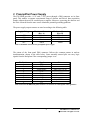
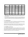
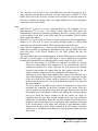
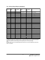
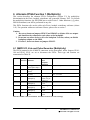
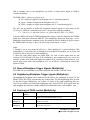
1
User's Manual PXI Power Distribution Module Version 2.5, June 2010 XIA LLC 31057 Genstar Road Hayward, CA 94544 USA Phone: (510) 401-5760; Fax: (510) 401-5761 http://www.xia.com Disclaimer Information furnished by XIA is believed to be accurate and reliable. However, XIA assumes no responsibility for its use, or for any infringement of patents, or other rights of third parties, which may result from its use. No license is granted by implication or otherwise under the patent rights of XIA. XIA reserves the right to change the DGF Pixie product, its documentation, and the supporting software without prior notice. Table of Contents 1 Overview......................................................................................................................................................3 2 Preamplifier Power Supply..........................................................................................................................4 3 Clock Distribution........................................................................................................................................5 3.1 Local clock only.....................................................................................................................................6 3.2 PXI PDM is clock master......................................................................................................................6 3.3 External clock is clock master...............................................................................................................7 3.4 Clock master on backplane....................................................................................................................8 4 Connections between Backplane and Front Panel.....................................................................................10 4.1 Description of Backplane Signals........................................................................................................10 4.2 PDM connections to Backplane ..........................................................................................................12 4.3 PDM Front Panel Connectors..............................................................................................................12 5 Standard FPGA functions...........................................................................................................................15 5.1 MMCX I/O, Veto and Pulse Generator (standard)..............................................................................15 5.2 Multiplicity and Star Trigger (standard)..............................................................................................18 5.3 Bussed Backplane Trigger Signals (standard).....................................................................................18 5.4 Neighboring Backplane Trigger signals (standard).............................................................................20 5.5 Summary of FPGA control (standard).................................................................................................21 5.6J 6 Front Panel Pinout (standard)..........................................................................................................22 6 Alternate FPGA Function 1 (Multiplicity).................................................................................................23 6.1 MMCX I/O, Veto and Pulse Generator (Multiplicity)........................................................................23 6.2 Multiplicity and Star Trigger (Multiplicity)........................................................................................24 6.3 Bussed Backplane Trigger Signals (Multiplicity)...............................................................................25 6.4 Neighboring Backplane Trigger signals (Multiplicity).......................................................................25 6.5 Summary of FPGA control (Multiplicity)...........................................................................................25 6.6 J6 Front Panel Pinout (Multiplicity)....................................................................................................26 7 Alternate FPGA Function 2 (Module Coincidence)..................................................................................27 7.1 MMCX I/O, Veto and Pulse Generator (Module Coincidence)..........................................................27 7.2 Multiplicity and Star Trigger (Module Coincidence)..........................................................................28 7.3 Bussed Backplane Trigger Signals (Module Coincidence).................................................................29 7.4 Neighboring Trigger signals (Module Coincidence)...........................................................................29 7.5 Summary of FPGA control (Module Coincidence).............................................................................29 7.6 J6 Front Panel Pinout (Module Coincidence)......................................................................................30 8 Alternate FPGA Function 3 (X-ray pulser)................................................................................................31 8.1 MMCX I/O, Veto and Pulse Generator (X-ray pulser).......................................................................31 8.2 Multiplicity and Star Trigger (X-ray pulser).......................................................................................32 8.3 Bussed Backplane Trigger Signals (X-ray pulser)..............................................................................32 8.4 Neighboring Trigger signals (X-ray pulser)........................................................................................32 8.5 Summary of FPGA control (X-ray pulser)..........................................................................................32 8.6 J6 Front Panel Pinout (X-ray Pulser)...................................................................................................33 9 Appendix....................................................................................................................................................34 9.1 Default Jumper settings........................................................................................................................34 9.2 Summary of FPGA control (standard).................................................................................................35 9.3 Summary of FPGA control (Multiplicity)...........................................................................................35 9.4 Summary of FPGA control (Module Coincidence).............................................................................36 9.5 Summary of FPGA control (X-ray Pulser)..........................................................................................36 2 PXI PDM User’s Manual V2.5 XIA 2010. All rights reserved. 1 Overview The PXI Preamplifier Power and Trigger Breakout Module (PXI PDM) is a module to support XIA’s Pixie-4 data acquisition modules. It is manufactured in a 3U CompactPCI/PXI form factor and can reside in any peripheral slot of a standard CompactPCI/PXI chassis, together with Pixie-4 modules or by itself. Slot 2, the PXI Star Trigger slot, is the preferred location, as it allows the use of some additional functions. The PXI PDM currently exists in two hardware revisions: Rev. A (serial numbers 100 through 124) and Rev. B (serial numbers 125 and above). This manual covers only Rev B modules. Manual Version 1.0 (June 2004) describes Rev. A modules. Though manufactured in the CompactPCI/PXI form factor, the PXI PDM does not have a PCI interface and is thus not recognized by the PCI bus controller or host computer. It only uses power from the PCI backplane and connects to the PXI backplane lines used for clock and trigger distribution by Pixie-4 modules. The power is used for a low noise power supply for preamplifiers; the clock and trigger lines can be brought to the PXI PDM front panel to connect to external electronics and/or can be controller by an on-board field programmable gate array (FPGA). The PXI PDM provides five principal functions, namely • • • • • Preamplifier power supply for the detector Clock distribution Access to backplane trigger signals Analog Pulser BGO pulse discriminator 3 PXI PDM User’s Manual V2.5 XIA 2010. All rights reserved. 2 Preamplifier Power Supply The PXI PDM provides +/-12V and +/-24V power through a DB9 connector on its front panel. This enables a compact experimental setup of detector and Pixie-4 data acquisition boards without the need for external power supplies. Moreover, powering the detector and the Pixie-4 boards from the same source eliminates potential grounding problems. The power supply output currents are rated according to the following table: Supply Voltage +12V -12V +24V -24V Maximum Current (Rev. A) 100mA 100mA 40mA 40mA Maximum Current (Rev. B) 250mA 100mA 40mA 40mA Table 1: Maximum currents for the preamplifier power supply. The pinout of the front panel DB9 connector follows the common pattern in nuclear instrumentation, shown in the table below. Some normally unused pins can carry logic signals from the backplane if the corresponding jumper is set. Pin Number 1 2 3 4 5 6 7 8 9 Signal GND GND EventTrigger +12V Veto -24V +24V Status (Time) -12V Notes Only if JP51 is set Only if JP52 is set Only if JP54 is set Table 2: Pinout of the DB9 front panel connector. See section 4 for a description of the signal lines 4 PXI PDM User’s Manual V2.5 XIA 2010. All rights reserved. 3 Clock Distribution In experimental setups with more than one Pixie-4 module, all Pixie-4 modules should run off the same clock to synchronize triggers and timestamps between them. There are a number of options to share clocks between Pixie-4 modules without the need for a PXI PDM module. The PXI PDM allows additional configurations. In particular, it allows input from and output to external clock sources. There are five possible clock sources for the PXI PDM: 1. The local clock crystal on the module 2. An external differential (LVDS) clock connected to the 2mm header behind the front panel 3. The PXI clock provided by the chassis. By default, it runs at a frequency of 10MHz and is only useful for Pixie-4 clock distribution if it has been overridden by a 37.5MHz clock signal. 4. A clock from a module distributed through a bussed backplane line 5. A clock from left neighboring module distributed through a daisy-chain One of these clock sources can be selected as an input to the PDM’s clock PLL circuit, which generates several copies of the input clock for different outputs. The clock outputs can be sent to one or more of the following recipients 1. One of the outputs is always connected to the PDM’s local FPGA 2. The PDM always sends out a differential (LVDS) clock to the 2mm header behind the front panel 3. The PDM can override the PXI clock created by the backplane, which is distributed through a low-skew clock path to all slots in the PXI chassis. 4. The PDM can send out the clock to a bussed backplane line to all slots in the chassis. 5. The PDM can send out the clock to the right neighboring slot. The different options for clock distribution are summarized in Table 3 and explained in detail below. In practice, the following three options should cover most applications: 1. The PXI PDM is not used for clock distribution, and runs of its local clock, as described in section 3.1 2. The PXI PDM, with its local clock source, is used to override the PXI clock from the backplane to distribute the clock signal to all modules, as described in section 3.2.1 3. The PXI PDM is used to run all modules in the chassis from an external clock, as described in section 3.3.1 5 PXI PDM User’s Manual V2.5 XIA 2010. All rights reserved. REV. B To local FPGA To front panel output To PXI clock override Slot 2 only Output to right neighbor To BUS clock output Local clock JP2: 3-4 Front panel input JP2: 3-5 PXI clock input JP2: 1-3 (slot 2 only) BUS input JP2: 7-8 Left neighbor input JP2: 7-9 Remove JP6 Left -> Right bypass JP2: pin 9 unconnected Remove JP6 always always always always always always always Not possible always always Not possible JP2: 10-12 Remove JP7, 10 JP2: 10-12 Remove JP7, 10 JP2: 10-12 Remove JP7, 10 JP2: 10-12 Remove JP7, 10 JP2: 10-12 Remove JP7, 10 JP2: 8-10 always JP2: 1-3, 4-6 Remove JP9 JP2: 1-3, 5-6 Remove JP9 Not possible Not connected Not connected Not possible Set JP10 Remove JP7 Not possible JP2: 8-10 JP2: 8-10 Not possible JP2: 8-10 Table 3: Summary of clock distribution options for the PXI PDM, Rev. B. Choose one of the input options (rows) and one of the three backplane output options, as described in detail below. Pin 1 is at the upper right of JP2. Note: For PXI clock override, the local clock or front panel clock is sent to the PXI backplane and then the PXI clock input from the backplane is used to drive the local FPGA and the front panel output. This ensures minimal clock skew between the PXI PDM and Pixie-4modules in the other slots. 3.1 Local clock only To run the PXI PDM from its local clock, independent of any other clocks in the system, set a shunt on jumper JP2 such that pins 3 and 4 are connected Any signal on the front panel clock input (pins 1 and 2 of the 2mm connector J6) will be ignored. Note that the front panel clock output (pins 15 and 16 of the 2mm connector) always carries a differential clock signal (LVDS). Other outputs (bussed clock, neighboring clock, and PXI clock are only active if the shunts on JP2 are set to connect pins 8 or 6 with other pins. 3.2 PXI PDM is clock master The PXI PDM can distribute its local clock to the other modules in the chassis in 3 different ways. An LVDS clock output signal is also always available on pins 15 and 16 of the 2mm header behind the front panel (J6) to distribute the clock to other chassis. Any signal on the front panel clock input (pins 1 and 2 of the 2mm connector) will be ignored in the settings described in this section. The three options for clock distribution are 6 PXI PDM User’s Manual V2.5 XIA 2010. All rights reserved. 3.2.1 Distribute local clock via PXI clock If the PXI PDM is located in slot 2 of the chassis, it can override the 10MHz clock provided by the backplane with its local clock. The backplane will distribute the local clock with low skew buffering to each slot in the chassis. This is the preferred configuration if slot 2 is available. To do so, set two shunts on jumper JP2 such that pins 1 and 3 as well as pins 4 and 6 are connected. Make sure that there is no shunt on JP9 to avoid conflict with any signal coming from the local FPGA 3.2.2 Distribute local clock via daisy-chained line If slot 2 is not available, the daisy-chained clock output can be used to send the clock to the neighboring module on the right, which will pass it on to its neighbor etc. For the PXI PDM to work as he clock master, all Pixie-4 modules have to be located to the right of the PXI PDM. To do so, set two shunts on jumper JP2 such that pins 3 and 4 as well as pins 10 and 12 are connected. Make sure that • shunts on JP7 and JP10 are removed to avoid conflict with any signal coming from the left and/or the local FPGA • the Pixie-4 boards are configured to use the daisy-chained clock as an input. 3.2.3 Distribute local clock via bussed line If the PXI PDM can not be in slot 2 or to the right of all Pixie-4 modules, it can send the external clock through a bussed clock line to all modules. This mode is not recommended for systems with more than three Pixie-4 modules. To do so, set two shunts on jumper JP2 such that pins 3 and 4 as well as pins 8 and 10 are connected. 3.3 External clock is clock master The PXI PDM can use an external differential (LVDS) clock signal, connected to pins 1 and 2 of the 2mm header behind the front panel for its local FPGA and distribute it to all modules in the chassis in 3 different ways. A repeated LVDS clock signal is available on pins 15 and 16 to distribute the clock to other chassis. The three most common options for clock distribution are distribution via the PXI clock path, via the daisy-chained lines, and via a bussed backplane line. Note: Both the front panel clock input and the clock output are LVDS differential signals. The signal amplitude is about 400mV. The incoming clock is terminated with 100Ohm between the two differential lines if JP1 is set. The outgoing clock has to be terminated likewise at the receiving end. For longer distances, a twisted or shielded cable is recommended, rather than the flat cable used for the trigger lines. 7 PXI PDM User’s Manual V2.5 XIA 2010. All rights reserved. 3.3.1 Distribute external clock via PXI clock If the PXI PDM resides in slot 2 of the chassis, it can override the 10MHz clock provided by the backplane with the external clock. The backplane will distribute the external clock with low skew buffering to each slot in the chassis. This is the preferred configuration if slot 2 is available. To do so, set two shunts on jumper JP2 such that pins 1 and 3 as well as pins 5 and 6 are connected. Set jumper JP1 to terminate the LVDS input with 100 Ohms. Make sure that there is not shunt on JP9 to avoid conflict with any signal coming from the local FPGA 3.3.2 Distribute external clock via daisy-chained line If slot 2 is not available, the daisy-chained clock output can be used to send the clock to the neighboring module, which will pass it on to its neighbor etc. For the PXI PDM to work as he clock master, all Pixie-4 modules have to be located to the right of the PXI PDM. To do so, set two shunts on jumper JP2 such that pins 3 and 5 as well as pins 10 and 12 are connected. Set jumper JP1 to terminate the LVDS input with 100 Ohms. Make sure that • shunts on JP7 and JP10 are removed to avoid conflict with any signal coming from the left and/or the local FPGA • the Pixie-4 boards are configured to use the daisy-chained clock as an input. 3.3.3 Distribute external clock via bussed line If the PXI PDM can not sit in slot 2 or to the right of all Pixie-4 modules, it can send the external clock through a bussed clock line to all modules. This mode is not recommended for systems with more than two Pixie-4 modules. To do so, set two shunts on jumper JP2 such that pins 3 and 5 as well as pins 8 and 10 are connected. 3.4 Clock master on backplane In cases where another module in the chassis is the clock master, the PXI PDM can connect to that clock and bring it out to the front panel as a differential clock. Pins 15 and 16 of the I/O connector behind the front panel always carry the clock output signal. The clock for the PDM’s FPGA is always connected to the selected inputs. The backplane master clock input can be selected as follows: 8 PXI PDM User’s Manual V2.5 XIA 2010. All rights reserved. 3.4.1 PXI clock input If the master clock is distributed through the PXI clock, set a shunt on jumper JP2 such that pins 1 and 3 are connected. Any signal to the front panel clock input (pins 1 and 2 of the 2mm connector behind the front panel) will be ignored. 3.4.2 Bussed clock input If the master clock is distributed by another module through the bussed clock line, set a shunt on jumper JP2 such that pins 7 and 8 are connected. Any signal to the front panel clock input (pins 1 and 2 of the 2mm connector) will be ignored. 3.4.3 Daisy-chained clock input If the clock is provided by the left neighbor, set a shunt on jumper JP2 such that pins 7 and 9 are connected. Any signal to the front panel clock input (pins 1 and 2 of the 2mm connector) will be ignored. Make sure that there is not shunt on JP6 to avoid conflict with any signal coming from the local FPGA To send out the clock to the right neighbor, set a second shunt on jumper JP2 such that pins 10 and 12 are connected. Make sure that shunts on JP7 and JP10 are removed to avoid conflict with any signal coming from the left and/or the local FPGA It is also possible to only pass through the clock from left to right without buffering and using it on the PDM To do so, do not connect pin 9 on JP2 to any other pin and set a shunt on JP10. Set the local clock as the input to the local FPGA by connecting pins 3 and 4. Make sure that shunts on JP6 and JP7 are removed to avoid conflict with any signal coming from the local FPGA. 9 PXI PDM User’s Manual V2.5 XIA 2010. All rights reserved. 4 Connections between Backplane and Front Panel The trigger signals of the Pixie-4 modules on the backplane can be accessed through the front panel MMCX connectors, the DB9 power connector, and/or the 2mm header J6 behind the front panel. An FPGA between the backplane and the front panel connectors acts as a configurable logic gate to combine or modify external and backplane signals. For direct access, several backplane lines can be directly connected to front panel connectors, i.e. bypassing the FPGA PXI PDM front panel connections. Section 4.1 describes the functions assigned to the backplane lines in standard a Pixie-4 system. Sections 4.2 and 4.3 describe the front panel connectors and PDM backplane connections. The connections made by the PDM’s FPGA in the current firmware are described in section 5. 4.1 Description of Backplane Signals The PXI lines on the backplane come in three different types: bussed lines, neighboring lines and the star trigger lines. Bussed backplane lines connect all slots of a PXI backplane. (In a chassis with more than 8 slots, the bussed lines can be divided in several segments, see manufacturer’s details.) Neighboring or daisy-chained backplane lines connect a module to its left and right neighbors. (In slot 2, which has no left neighbor except the PCI controller, the lines going to the left are used for the Star Trigger.) The “Star Trigger” lines on the PXI backplane connect each of slots 3-15 with a dedicated line to slot 2. 4.1.1 Bussed backplane lines 4.1.1.1 Wire-OR lines In the Pixie-4 trigger setup, five of the bussed backplane lines are used as wire-OR busses (active low with pullup) to distribute triggers, synchronization signals, and module coincidence information: Fast Trigger, Event Trigger, Sync, Token, and Status (previously called Time). • • • Fast Trigger signals that in at least one Pixie-4 module an input signal pulse crossed over the trigger threshold. The Fast Trigger signal is used to stop the FIFOs for waveform acquisition in all modules simultaneously. Event Trigger signals that a pulse passed pileup inspection and is indeed a pulse with a valid energy measurement. This signal causes an interrupt in the Pixie-4 DSP to read out and process the event data. Sync is used to start and stop runs synchronously. While a module is setting up a data acquisition run (clearing memory, resetting pointers, etc), it pulls this line low. When ready to take data, the line is released. The last module to release the line lets it go high, which signals a runstart to all modules. The first module to 10 PXI PDM User’s Manual V2.5 XIA 2010. All rights reserved. • finish a run pulls the line low again to stop the data acquisition in all other modules. Token and Status can be used by a module to indicate that for a given event, the channels meets a user defined hit pattern. 4.1.1.2 Veto line The Pixie-4 modules use an additional bussed backplane line to distribute a Veto signal. This signal, typically generated by an external source, is driven on the Veto line either by the Pixie-4 through its front panel input, by the PDM, or by another device. If the Veto line is high, it inhibits event triggers in those channels of Pixie-4 modules that have the GFLT bit set (see Pixie-4 user manual). Since only event triggers are inhibited, the time between fast trigger (the leading edge of the pulse) and event triggers (a time T ET = Tpeak +Tgap later) can be used to make the Veto decision. On the other hand, this means that at any given moment, a Veto signal inhibits pulses that occurred a time TET earlier. To allow vetoing on a pulse by pulse basis, the current PDM firmware includes a (limited) delay feature, see section 5.1.4. 4.1.1.3 Bussed Clock A further bussed backplane line can be used to distribute a clock signal. This is not recommended for systems with more than 3 Pixie-4 modules. See section 3 for details. 4.1.2 Neighboring backplane lines 4.1.2.1 Clock In a Pixie-4 system, one pair of the neighboring lines (PXI_LBR0 and PXI_LBL0) can be used for clock distribution. The clock coming in from the left neighbor can be configured as the module’s clock input and sent out to the right neighbor. 4.1.2.2 Trigger Three pairs of the neighboring lines (PXI_LBR/L 8-10) are used to distribute trigger information and run synchronization (for chassis with bus segment boundaries disconnecting the wire-OR lines). The lines are used to form a “chained-OR” – each module ORs its right input with its local contribution and sends it out to the left. 4.1.2.3 Module Coincidence Two neighboring lines (PXI_LBL 2-3) are used to by a Pixie-4 module in slot 3 to a) specify a particular module coincidence decision for a PXI-PDM in slot 2 and b) to control the coincidence window for the module coincidence. PXI_LBR2-3 are connected to the Pixie-4 system FPGAs, but currently unused and but reserved. 11 PXI PDM User’s Manual V2.5 XIA 2010. All rights reserved. 4.1.2.4 Channel Gate In hardware revision D of Pixie-4 modules (S/N 250 and above), 4 neighboring lines (PXI_LBL4-7) are used to receive a channel specific GATE signal to from a neighboring module (e.g. a PXI PDM). Similar to the VETO function, a channel only records events if the GATE input is high (or low). PXI_LBR4-7 are connected to the Pixie-4 trigger/filter FPGAs, but currently unused and but reserved. 4.1.3 Star Trigger lines The Star Trigger are used by the Pixie-4 modules to send multiplicity information to slot 2. 4.2 PDM connections to Backplane 4.2.1 Bussed backplane lines On the PXI PDM, all bussed backplane lines are connected to the FPGA. Table 4 summarizes those lines that can optionally be connected directly to a front panel connector (bypassing the FPGA). The functions of the lines are described above in sections 4.1.1.1 4.1.1.3, the FPGA operation in section 5 4.2.2 Neighboring backplane lines All PXI neighbor lines are connected to the PDM’s FPGA. For all PXI neighbor lines, there are bypass jumpers (JP10-22) on the PXI PDM, to directly connect lines to/from the left to the corresponding lines from/to the right. When setting bypass jumpers, make sure the operation of the FPGA (as described in section 5) is compatible. In particular, do not set the bypass jumpers if the module is in slot 2. One pair of the neighboring lines (PXI_LBR0 and PXI_LBL0) is normally used for clock distribution and should be disconnected from the FPGA by removing shunts from JP6 and JP7, unless explicitly used by the FPGA (e.g. to build the multiplicity in slot 2). For details of the clock distribution, see section 3. 4.2.3 Star Trigger lines As all left neighbor inputs are connected to the FPGA, the PXI PDM receives the Star Trigger signals from slots 3-15 when located in slot 2. FPGA Operation of the FPGA is described in section 5. The PDM also connects to the Star Trigger line so it can send out Star Triggers to slot 2 if located in slot 3-15. If located in slot 2, this line is used as the clock input to the PXI backplane. It should therefore be disconnected from the FPGA by removing any shunts from JP9. 12 PXI PDM User’s Manual V2.5 XIA 2010. All rights reserved. 4.3 PDM Front Panel Connectors Note: Care should be taken to only connect appropriate 3.3V signals at the front panel inputs and to avoid shorts on the signal outputs, as they are connected directly to the FPGA or the backplane with no intermediate buffers! Front panel connectors on the PXI PDM include 8 MMCX connectors, the DB9 power connector, and the 2mm header J6 behind the front panel. Normally the FPGA between the backplane and the front panel connectors acts as a configurable logic gate to combine and/or buffer signals to and from the backplane, as described in section 5. However, the FPGA can be bypassed and several front panel connectors can connect directly to the backplane, as described in section 4.3.4. 4.3.1 MMCX connectors Of the 8 small coaxial MMCX front panel connectors, connectors 1-3 are always outputs controlled by the FPGA. Connectors 4 and 5 can be either inputs to or outputs from the FPGA or alternatively connect directly to a PXI backplane line. Connectors 6-8 are either inputs to the FPGA or connect directly to a PXI backplane line. If connecting directly to the backplane, make sure the FPGA is in a compatible mode! 4.3.2 DB9 power connector In the DB9 power connector, 6 pins are used to provide power and ground for preamplifiers. The remaining 3 pins are normally not used in nuclear physics applications and can be connected directly to a PXI bussed backplane line, as listed in Tables 2 and 4. 4.3.3 2mm header J6 The 30 pins of the header behind the front panel (J6) include input and output signals, ground and power, as listed in table 7. Normally all input and output signals connect to the FPGA, but some of the inputs can be configured to also connect directly to a PXI bussed backplane line. If using this option, make sure the FPGA is in a compatible mode! The connector is a vertical header with 2mm pitch. A matching receptacle is for example Molex part number 87568-3093. Usually signals will be brought out to some external electronics with a 30x flat cable. The external electronics can then distribute clocks and triggers among several chassis with Pixie-4 modules or connect to external devices. With some limitations, inputs and outputs can also be daisy-chained with a 14x flat cable from chassis to chassis. For complete trigger distribution, the daisy-chain should be closed back from the last to the first chassis, however as described below, the Sync line can not be closed from the last to the first module. Furthermore, any external input signal (such as veto) has to be introduced at some point into the daisy-chain. 13 PXI PDM User’s Manual V2.5 XIA 2010. All rights reserved. 4.3.4 Direct Connections from Front panel to Backplane As mentioned above, several backplane lines can be directly connected to front panel connectors, i.e. bypassing the FPGA. These lines and front panel connectors are listed in Table 4. Front Panel connector MMCX 8 MMCX 7 MMCX 6 MMCX 5 MMCX 4 DB9, pin 3 DB9, pin 5 DB9, pin 8 J6, pin 4 J6, pin 5 J6, pin 6 J6, pin 7 J6, pin 8 J6, pin 9 Backplane line Connected by Veto Status (Time) Event Trigger Fast Trigger Sync, Token or Fast Trigger Event Trigger Veto Status (Time) Fast Trigger Event Trigger Veto Sync Status (Time) Token JP101 JP102 JP103 JP104 JP110, JP111 JP51 JP52 JP54 JP40 JP41 JP42 JP43 JP44 JP45 Table 4: List of front panel connectors that can be directly connected to a PXI backplane line. Lines have several front panel options since connectors can be used for other purposes also. Note: When connecting pins in J6 to the backplane, ensure compatibility with FPGA operation (disable FPGA outputs to backplane). 14 PXI PDM User’s Manual V2.5 XIA 2010. All rights reserved. 5 Standard FPGA functions The configuration of the FPGA can be adapted to specific applications. Below we describe the standard configuration PDM 2.0, generated November 2006. Other FPGA variants are described in sections 6 and 7. For custom configurations, please contact XIA. 5.1 MMCX I/O, Veto and Pulse Generator (standard) The FPGA connects to the 8 MMCX connectors on the front panel, unless Jumpers JP101104 and JP110, JP111 are set to disconnect the FPGA. Their type and function are summarized in Table 5a: MMCX FPGA Direction FPGA Function 1 Output 2 Output 3 Output analog pulses (fixed pulse shape) analog pulses (DAC) logic pulses (high load) logic pulses Alternate direct backplane connection -- Control -- J10 – trigger source JP400 – decay time -- J10 – assign outputs 3-5 to a) logic pulse related to analog pulses Fast Trigger, b) output of BGO discriminator Token, or Sync c) multiplicity JP110, 111 d) periodic pulses 5 Output logic pulses Fast Trigger JP104 6 Input unused Event Trigger JP103 7 Input external trigger Status (Time) JP102 8 Input BGO discriminator Veto JP300-304 – discriminator settings Veto JP101 J10 – Veto pulse length and delay Table 5a: MMCX connector functions (standard). See tables 6a and 7a for control settings. 4 Output 5.1.1 Analog pulser outputs on MMCX 1-2 (standard) MMCX Connector 1 is an output for analog pulses controlled by the FPGA. The rise time is about 20ns. JP401 controls its decay time. The decay is about 500ns if JP400 is removed, otherwise about 10µs. The amplitude is about 100mV. The signal has an approximate 10% undershoot, and this pulse is intended mainly for testing of coincidence acquisition rather than for high resolution spectroscopy. The output is driven by an opamp with 50 Ohm serial termination and capable of driving higher loads. MMCX Connector 2 is the output of a high speed DAC controlled by the FPGA. The output is driven by an opamp with 50 Ohm serial termination and capable of driving higher loads. The PDM’s FPGA can in principle set the output of MMCX 2 to an arbitrary analog voltage at every clock cycle (with 13bit precision). In the current firmware, the DAC is set to generate exponentially decaying pulses of amplitude ~200mV amplitude with a rise time of 15 PXI PDM User’s Manual V2.5 XIA 2010. All rights reserved. ~50ns and a decay time of 27µs). If desired, the firmware can be modified to generate a wide variety of pulse shapes. Both pulses can be triggered either by an internal pseudo-random generator at an average rate of about 9000 counts/s, periodically every ~200µs or by an external logic pulse fed into to MMCX connector 7. The trigger mode is controlled by setting shunts on J10 as listed in Table 7a. When using the Pixie-4 module to acquire MCA spectra from the PDM’s pulse generator, the following settings achieve good results (PDM and Pixie-4 in the same chassis): Setting Tpeak Tgap Decay time τ Gain Filter range Resolution (external periodic, 5kcps) Resolution (internal random, 9kcps) MMCX 1 (without JP400) 12.5µs 0.8µs 4.7µs 4 3 ~0.4% ~5% (due to undershoot) MMCX 2 (DAC) 24.96µs 1.28µs 27.25µs 4 4 ~ 0.12% ~0.14% To reduce cross talk from the logic pulser (which may lead to shoulders on the peak and/or worse resolution), it is recommended to disable the logic outputs, e.g. by setting a shunt on pin 11 of J10 to output only BGO and module coincidence logic with no inputs for these signals connected or enabled. 5.1.2 Logic outputs on MMCX 3-5 (standard) MMCX Connector 3 can only be used as an output. It is driven by an opamp with 50 Ohm serial termination and capable of driving higher loads. Normally, it is a 3.3V logic output, but – if really desired – JP401 can be removed to add a decay at the end of the pulse, thus imitating a detector signal. MMCX Connectors 4 and 5 are currently used as a logic outputs (but can be used as inputs in modified firmware). They are driven by the FPGA and therefore can handle only a limited load. Connector 4 is the same FPGA I/O as pin 28 of J6 In the current firmware, connectors 3-5 are assigned one of four signals generated by the FPGA. Shunts on J10 control which signal is assigned to which connector, see table 7a. The four signals are a) a logic pulse related to the analog pulser signals b) the module multiplicity obtained from the StarTrigger signals (see section 5.2) c) the logic pulse generated by the BGO discriminator and (section 5.1.4) d) a periodic trigger 5.1.3 Logic inputs on MMCX 6-7 (standard) MMCX Connectors 6-7 can only be used as logic inputs. The current use for connector 7 is to accept an external trigger for the PDM pulser circuits. Connector 6 is currently unused. 16 PXI PDM User’s Manual V2.5 XIA 2010. All rights reserved. 5.1.4 BGO discriminator or Veto input on MMCX 8 (standard) Note: Only one device may drive the Veto backplane line to avid I/O conflicts. If using the PDM to drive the Veto line, make sure the Pixie-4 modules do not. Connector 8 can only be used as an input, but it accepts either a logic pulse or uses a discriminator to convert an analog pulse (from a BGO shield) into a logic pulse. The logic pulse is then stretched, delayed, and sent to the Veto backplane line to inhibit data acquisition in the Pixie-4 modules (see section 4.1.1.2.) To connect an external Veto signal to the backplane without modification, set JP101 to “Veto” (bypassing the FPGA) and remove the shunt from pin 17 of J10 to J13 (disabling the FPGA’s output to the Veto backplane line). If JP101 is set to “FPGA”, the input signal on MMCX 8 is either connected directly to the FPGA or to the BGO discriminator circuit which converts an analog pulse into a logic pulse for the FPGA. Jumpers JP302 and JP303 control this connection, see table 6. The FPGA will drive the Veto backplane low (to allow data acquisition) unless it detects a rising edge at the MMCX input. The rising edge will cause the FPGA to drive the Veto line high for 4µs (1µs) after 4µs (1.5µs), depending on J10. (This stretched signal is OR-ed with the Veto input on J6.) The rising edge will trigger a short output pulse on one of MMCX connectors 3-5. In the default hardware configuration, the BGO discriminator triggers on pulses greater than approximately 3mV, typically about 50ns after the rising edge of the analog pulse (propagation delays). Pulses of either polarity are accepted by setting JP 300 and JP301. (However, the discriminator may also trigger on the opposite polarity with an additional ~200ns delay). Mode enable vetoenable longveto logic BGO Positive Negative Jumper setting connect J10 pin 1 to J13 connect J10 pin 17 to J13 connect J10 pin 3 to J13 JP302 = 1-2 (“logic”) JP303 = 2-3 JP302 = 2-3 (“BGO”) JP303 = 1-2 JP300 = 2-3 (at “+”) JP301 = 2-3 (not “+”) JP300 = 1-2 (not “+”) JP301 = 1-2 (at “+”) BGO discriminator / Veto function if connected, enables output to all backplane lines if connected, enables output to Veto backplane line (pin 1 and 17 must be connected to J13 to enable Veto output) if connected, the backplane Veto pulse is 4µs long after a 4µs delay, else it is 1µs long after 1.5µs delay Connect logic signal on MMCX 8 to FPGA Connect analog pulse on MMCX 8 to discriminator circuit and discriminator output to FPGA Trigger on positive edge of analog pulse Trigger on negative edge of analog pulse Table 6a: BGO discriminator and Veto control settings. Note that JP300 and 301 are always opposite (as well as JP302 and JP303). Note: It is possible to add a daughterboard to add the BGO discriminator function to inputs 2-4, thus generating 4 veto signals for the 4 channels of a Pixie-4 module. Please contact XIA for details. 17 PXI PDM User’s Manual V2.5 XIA 2010. All rights reserved. 5.2 Multiplicity and Star Trigger (standard) The PXI PDM connects to all left neighbor inputs on the backplane. Therefore, if located in slot 2, it can receive multiplicity information send by the Pixie-4 modules in slots 3-14 during the module coincidence test through the Star Trigger lines (see Pixie-4 user manual). In the current standard implementation, the PDM sums the number of Star Trigger signals to build the multiplicity M of Pixie-4 modules participating in an event. If M is greater than a user defined value N, the FPGA drives down the backplane Token line to signal back to the Pixie-4 modules. The backplane output can be disabled and N can be set to 3 or 4 by setting shunts on J10 (see table 7a). In addition, whenever M > N the FPGA will issue a short output pulse on one of MMCX connectors 3-5. Notes: 1. The state of the Token line is repeated back to J6 (pin 27) 2. When located in slots 3-18, the PXI PDM itself currently does not use the StarTrigger line connecting to slot 2. 5.3 Bussed Backplane Trigger Signals (standard) Note: While the distribution of bussed trigger signals as implemented in the FPGA allows in principle to connect two or more chassis, its main purpose is to bring out the signals to external electronics via J6 for advanced users. The trigger distribution on the wire-OR lines and between chassis can be improved from the current implementation (unchanged from version 1.0) if required. The preferred method of connecting external signals to the bussed trigger lines is to set jumpers JP101-104 and JP110-111 to directly connect MMCX connectors 4-8, see table 5a. However, if driving the backplane lines from an external device, the FPGA outputs to the backplane muse be disabled by removing the shunt from J10. Wire-OR lines may be driven low, but the Veto line must not be driven high or low unless both the PDM’s FPGA and the Pixie-4 are disabled to drive it. The PDM’s FPGA connects to 20 pins on the 2mm header behind the front panel (J6), of which 10 are configured as inputs and 10 are configured as outputs. (The remaining pins of J6 are power, ground, or clock signals). The detailed pin assignment is listed in table 8a. The FPGA connects the inputs and outputs on J6 with the bussed backplane trigger lines and a limited number of neighboring lines. The following functions are implemented: • For Fast Triggers and Event Triggers, the falling edge of a pulse on J6 will cause the FPGA to drive the corresponding backplane line low for ~100ns pulse (to avoid locking up lines). The backplane line is normally pulled high by a Pixie-4 module. The output on J6 is equal to the corresponding backplane line. • The Sync, Token, and the Status (Time) backplane lines will be driven low for as long as their front panel input is low. If the front panel input goes high, the backplane line may still be driven low by a module in the chassis. In addition, the Token line may be pulled low by the FPGA if the multiplicity M is greater than a user defined value N (if enabled). The output on J6 is equal to the backplane line. 18 PXI PDM User’s Manual V2.5 XIA 2010. All rights reserved. • The veto line is driven high or low by the PDM based on either the input on J6 or (logic OR) the stretched pulse generated from the rising edge on MMCX 8. If the PDM’s FPGA drives the Veto line, no other device may drive it; therefore make sure the Pixie-4 modules do not have their veto output enabled and no direct backplane connection is used on the PDM. Notes: 1. With JP40-45, 6 pins of J6 can be connected directly to the backplane also (to backplane lines FT, ET, Sync, Veto, Status, Token). When the FPGA drives the backplane lines, this has the potential of locking up the lines, since the FPGA output to the backplane is fed back to the FPGA input for the backplane. JP40-45 should thus be used with caution. 2. With JP30-35, 6 of the inputs on J6 can be directly connected to the corresponding 6 outputs on J6. This may be useful for passing through signals in a daisy-chain connection, but will conflict with the FPGA outputs in the current firmware. 3. Since only one backplane line is used for run synchronization, it is not possible to inhibit runs externally (by pulling the backplane low through the PDM) and at the same time know if the Pixie-4 modules are not ready (pulling the line low themselves). This means that in the current implementation, either the PDM output is used to know the status of the backplane, or the PDM input is used to inhibit data acquisition. Limited run synchronization in a multiple chassis system can be set up in 2 ways: - Either the Sync inputs of all PDMs are controlled in parallel by external electronics, which inhibits data acquisition for an estimated time until all modules are assumed to be ready. While the run is in progress, the external electronics can monitor the signals from the Sync outputs, and stop the run whenever the first output goes low (by pulling the Sync inputs low). - Alternatively, crates can be daisy-chained (Sync output of one PDM to Sync input of the following PDM). The daisy-chain can not be closed from the last to the first PDM as the system could be locked in an inhibited state. The modules and chassis have to be set up such that the first chassis is in control of the synchronization The Sync output of the PDM in first chassis is determined by state of the backplane line controlled by the Pixie-4 modules in the chassis. While the Pixie-4 modules are not ready to take data, the Sync output will be low and thus inhibit the second chassis, which in turn inhibits the following chassis and so on. When the Pixie-4 modules in the first chassis are ready, its backplane Sync line goes high and the modules in the first crate will begin taking data. The PDM Sync output line will also go high, and if all the Pixie-4 modules in the second chassis were ready before, data acquisition will begin in the second chassis at the same time, and also in any additional chassis further down the daisy chain. When a module in the first chassis is finished with the run, it will inhibit all modules in its chassis and also further down the daisy-chain. 19 PXI PDM User’s Manual V2.5 XIA 2010. All rights reserved. 5.4 Neighboring Backplane Trigger signals (standard) All neighboring backplane lines connected to the FPGA are configured as inputs for the PDM’s FPGA; the FPGA is not driving any of these lines. The left neighboring lines are used for the Star Trigger Multiplicity, see section 5.2. Of the right neighboring lines, PXI_LBR8-10 are passed on to J6, the 2mm header behind the front panel, the rest are unused. See table 8a for the detailed pin assignment. 5.5 Summary of FPGA control (standard) Mode Enable Longveto Multi4 Connect J13 to J10 pin 1 3 5 Function If connected , enable outputs to bussed backplane lines, else disable. If connected, generate veto pulse after 4µs for4µs, else after 1.5µs for 1µs. If connected, require at least 4 Star Trigger signals to generate multiplicity signal, else require at least 3 Pulse out Neither 9 nor 11 MMCX 3 = logic pulser MMCX 4 = multiplicity MMCX 5 = BGO discriminator Multiplicity 11 only MMCX 3 = multiplicity out MMCX 4 = BGO discriminator MMCX 5 = logic pulser BGO out 9 only MMCX 3 = BGO discriminator MMCX 4 = logic pulser MMCX 5 = multiplicity Pulse and 9 and 11 MMCX 3 = logic pulser periodic out MMCX 4 = BGO discriminator MMCX 5 = periodic (200µs) External, no 13 only MMCX 1 = periodic (200µs) coincidence MMCX 2 = triggered by MMCX 7 logic pulser = periodic, same as MMCX 1 External, 13 and 15 MMCX 1 = triggered by MMCX 7, delayed ~500ns coincidence MMCX 2 = triggered by MMCX 7 logic pulser = triggered by MMCX 7, delayed ~500ns Internal, 15 only MMCX 1 = random, delayed to MMCX 2 by ~500ns coincidence MMCX 2 = random logic pulser = random, coincident with MMCX 2 Internal, no neither 13 nor 15 MMCX 1 = periodic (200µs) coincidence MMCX 2 = random logic pulser = random, delayed to MMCX 2 by ~500ns Vetoenable 17 If connected , enable outputs to Veto backplane line, else disable. (pin 1 and 17 must be connected to J13 to enable Veto output) P4test 19 Reserved for test mode Table 7a: Shunts on J10 to control FPGA operation. Connect each pin to the neighboring pin on J13 to activate a function. Pin 0 of J10 is the upper right pin, closest to the backplane connector and to the edge of the board. (The PCB label “1” refers to the upper left pin of J10) Note: 1. To generate periodic pulses on the DAC output, set shunts on pins 9, 11, and 13, optionally 15, and connect MMCX 5 to MMCX 7. 20 PXI PDM User’s Manual V2.5 XIA 2010. All rights reserved. 5.6 J6 Front Panel Pinout (standard) Front panel pin Split cable line Front panel Backplane pin Backplane Pixie function connection name connection type type 1 1A Clock In LBR0, TRIG7, to right, clock (depending on JP2 or PXI CLK bussed, or all jumper setting 2 2A Clock In* 3 3A GND 4 4A Input TRIG0 bussed Fast Trigger 5 5A Input TRIG1 bussed Event Trigger 6 6A Input TRIG2 bussed Veto 7 7A Input TRIG3 bussed Sync 8 8A Input TRIG4 bussed Status (Time) 9 9A Input TRIG5 bussed Token 10 10A GND 11 11A reserved 12 12A reserved 13 13A reserved 14 14A reserved 15 1B Clock Out 16 2B Clock Out* 17 3B GND 18 4B Output TRIG0 bussed Fast Trigger 19 5B Output TRIG1 bussed Event Trigger 20 6B Output N/A1 Veto 21 7B Output TRIG3 bussed Sync 22 8B Output TRIG4 bussed Status (Time) 23 9B Output LBR8 From right Chained OR Sync 24 10B GND 25 11B Output LBR9 From right Chained OR ET 26 12B Output LBR10 From right Chained OR FT 27 13B Output TRIG5 bussed Token 28 14B Output no backplane, same as MMCX 4 BGO, pulser, multiplicity 29 N/A 3.3V 30 N/A 5V Table 8a: Pinout of the 2mm front panel I/O connector (J6) in standard FPGA configuration. The signals can either be brought out to external electronics, or inputs and outputs can be connected from PDM to PDM with a split cable. When looking at the front panel, pin 1 is to the top and right. Note: If a split cable is used, Veto out (6B) should connect directly to Veto in (6A) using JP32; not driven by FPGA or backplane. 21 PXI PDM User’s Manual V2.5 XIA 2010. All rights reserved. 6 Alternate FPGA Function 1 (Multiplicity) This section describes the alternate FPGA configuration (version 2.3) for multiplicity discrimination in the Pixie-4 module coincidence test, generated February 2007. To perform the multiplicity functions, the PXI PDM has to reside in slot 2. Other functions (e.g. pulser, BGO discriminator) can still be performed in any slot. This FPGA function relies on the older style Pixie-4 module coincidence software (release 1.41). For operation with newer software releases, please refer to section 7. Caution: 1. Do not set shunts on jumpers JP30-35 and JP40-45 as all pins of J6 are outputs and should not be connected to each other or the backplane. 2. Do not use any other device to drive the backplane Veto line, unless you disable backplane outputs on the PDM. 3. If in slot 2, do not set shunts on jumpers JP10-22. 6.1 MMCX I/O, Veto and Pulse Generator (Multiplicity) The FPGA connects to the 8 MMCX connectors on the front panel, unless Jumpers JP101104 and JP110, JP111 are set to disconnect the FPGA. Their type and function are summarized in Table 5b: MMCX FPGA Direction FPGA Function 1 Output 2 Output 3 Output analog pulses (fixed pulse shape) analog pulses (DAC) Multiplicity (Token) External Multiplicity Alternate direct backplane connection -- Control JP400 – decay time --- J10 – see below Fast Trigger, Token, or Sync JP110, 111 5 Input External Fast Trigger Multiplicity JP104 6 Input External Event Trigger Multiplicity JP103 7 Input External Status (Time) Multiplicity JP102 8 Input BGO discriminator Veto JP300-304 – discriminator settings Veto JP101 Table 5b: MMCX connector functions. See tables 6a and 7b for control settings. 4 Input 22 PXI PDM User’s Manual V2.5 XIA 2010. All rights reserved. 6.1.1 Analog pulser output on MMCX 1-2 (Multiplicity) The analog pulser functions the same as in the standard configuration, but is always fixed in mode “internal, non-coincident”, i.e. MMCX 1 = 100mV, periodic (200µs) MMCX 2 = 200mV, random 6.1.2 Multiplicity inputs and outputs on MMCX 3-7 (Multiplicity) See section 6.2 6.1.3 BGO discriminator or Veto input on MMCX 8 (Multiplicity) Note: Only one device may drive the Veto backplane line to avid I/O conflicts. If using the PDM to drive the Veto line, make sure the Pixie-4 modules do not. Connector 8 can only be used as an input, but it accepts either a logic pulse or uses a discriminator to convert an analog pulse (from a BGO shield) into a logic pulse. The logic pulse is not stretched or delayed, but is sent directly to the Veto backplane line to inhibit data acquisition in the Pixie-4 modules (see section 4.1.1.2.) Since the input has an internal pullup, the PDM will always drive the Veto backplane line high if the input is not connected. Do not use any other device to drive this line, unless you disable backplane outputs. BGO discriminator control is the same as described in section 5. 6.2 Multiplicity and Star Trigger (Multiplicity) The PXI PDM connects to all left neighbor inputs on the backplane. Therefore, if located in slot 2, it can receive multiplicity information send by the Pixie-4 modules in slots 3-14 during the module coincidence test through the Star Trigger lines (see Pixie-4 user manual). In this configuration, slots 3 - 11 are designated "clover modules" and slots 12-18 are designated "LEPS modules". Therefore the maximum number of clover modules is 9, the maximum number of LEPS modules is 7. It is always possible to use fewer modules, so the number of clover or LEPS modules can be varied by filling up to the left and right from the slot 11-12 boundary. Modules have to be next to each other to share clocks and triggers. Therefore, since the first module has to sit in the first segment of the chassis (i.e. at most slot 6), one needs at least 6 clover modules to use modules in the LEPS slots. However, they can always be passive modules with no signals attached, as they are only needed to pass through the clocks and triggers. Slots 3-14 signal to the PDM through the backplane if they have a hit in one or more channels, if that option is selected in the Igor "chassis option panel". Slots 15-18 do not have a dedicated line in the PXI standard, so instead a Pixie-4 front panel output “I/O” has to be connected to a PDM front panel input to contribute to the multiplicity. There is no software control for this connection; a Pixie-4 always sends out a pulse on the front panel if the "share pattern" is met, if not used, just disconnect the cable. It is therefore possible to include 4 external signals from anywhere in the multiplicity. However, since these 4 inputs have automatic pull-ups on the PDM, if nothing is connected they appear always as "hit". This 23 PXI PDM User’s Manual V2.5 XIA 2010. All rights reserved. adds a constant value to the multiplicity (see below). Connect these inputs to GND to override the pullups. The PDM builds 3 values every clock cycle: M_all = number of signals from backplane slot 3-14 and front panel 0-3 M_clover = number of signals from backplane slot 3-11 M_LEPS = number of signals from backplane slot 12-14 and front panel 0-3 The user can set jumpers to define the minimum required signals in each group (N_all, N_clover, N_LEPS) to a value between 0 and 7. At any time when the condition C = (M_all >= N_all) & (M_clover >=N_clover) & (M_LEPS >= N_LEPS) is met, the PDM will set the TOKEN backplane line to logic 1 and also duplicate the TOKEN signal on a front panel connector MMCX3. The multiplicity outputs are kept logic 1 a few hundred ns longer than the condition is met. By setting the Pixie-4 modules in Igor to require the TOKEN line to be logic 1, they will only accept events where C is met. Notes: 1. Setting N_xxx to zero means the (M_xxx >= Nxxx) portion of C is met at all times. This means that e.g. if you don't care to distinguish clovers and LEPS modules, set N_clover and N_LEPS to zero to only test for total multiplicity. 2. Since the front panel inputs are pulled high: For each of these inputs that are not connected, N_LEPS and N_all have to be increased by one to not accept every event. For example, if none of the front panel inputs are connected, M_all will be always at least 4, so to acquire only events with a real multiplicity of 2, set M_all to 6. (Alternatively connect the inputs to GND). 6.3 Bussed Backplane Trigger Signals (Multiplicity) The PDM does not contribute to any other backplane line besides Veto and Token. 6.4 Neighboring Backplane Trigger signals (Multiplicity) All neighboring backplane lines connected to the FPGA are configured as inputs for the PDM’s FPGA; the FPGA is not driving any of these lines. The left neighboring lines are used for the Star Trigger Multiplicity, see section 6.2. None of the right neighboring lines are used. Do not connect left and right neighboring lines using JP10-22, else signals from the right neighbor may interfere with the multiplicity information on the “left neighbor” pins. 6.5 Summary of FPGA control (Multiplicity) Mode Enable Overall Multiplicity Clover Multiplicity Connect J13 to J10 pin 1 3,5,7 9,11,13 Function If connected , enable outputs to bussed backplane lines, else disable. Note no dedicated enable for Veto! Set minimum required overall multiplicity Na from 0-7. Pins 3-7 are bits 0-2 of N_all Set minimum required clover multiplicity Nc from 0-7. Pins 9-13 are bits 0-2 of N_clover 24 PXI PDM User’s Manual V2.5 XIA 2010. All rights reserved. LEPS 15,17,19 Set minimum required overall multiplicity Nl from 0-7. Pins 15Multiplicity 19 are bits 0-2 of N_leps Table 7b: Shunts on J10 to control FPGA operation. Connect each pin to the neighboring pin on J13 to activate a function. Pin 0 of J10 is the upper right pin, closest to the backplane connector and to the edge of the board. (The PCB label “1” refers to the upper left pin of J10) 6.6 J6 Front Panel Pinout (Multiplicity) Front panel pin 1 2 3 4 5 6 7 8 9 10 11 12 13 14 15 16 17 18 19 20 21 22 23 24 25 26 27 28 29 30 Front panel connection type Clock In Clock In* GND Output Output Output Output Output Output GND Output Output Output Output Clock Out Clock Out* GND Output Output Output Output Output Output GND Output Output Output Output 3.3V 5V Function clock (depending on JP2 jumper setting Multiplicity hit from slot 3 Multiplicity hit from slot 4 Multiplicity hit from slot 5 Multiplicity hit from slot 6 Multiplicity hit from slot 7 Multiplicity hit from slot 8 Multiplicity hit from slot 9 Multiplicity hit from slot 10 Multiplicity hit from slot 11 Multiplicity hit from slot 12 Multiplicity hit from slot 13 Multiplicity hit from slot 14 External multiplicity from MMCX7 External multiplicity from MMCX6 External multiplicity from MMCX5 Multiplicity sum of clover slots (3-11) Event Trigger on Backplane Multiplicity sum of all slots (3-15 and external) Multiplicity sum of LEPS slots (12-15 and external) External multiplicity from MMCX4 Table 8b: Pinout of the 2mm front panel I/O connector (J6) in multiplicity configuration. Do not set shunts on jumpers JP30-35 and JP40-45 as all pins of J6 are outputs and should not be connected to each other or the backplane. 25 PXI PDM User’s Manual V2.5 XIA 2010. All rights reserved. 7 Alternate FPGA Function 2 (Module Coincidence) This section describes the alternate FPGA configuration (version 2.7) for Pixie-4 module coincidence test, generated December 2008. To perform the module coincidence functions, the PXI PDM has to reside in slot 2. Other functions (e.g. pulser, BGO discriminator) can still be performed in any slot. The Module coincidence functions rely on Pixie-4 software 1.50 and higher. Caution: 1. Do not use any other device to drive the backplane Veto line, unless you disable backplane outputs on the PDM. 2. If operated in slot 2, do not set shunts on jumpers JP10-22. 7.1 MMCX I/O, Veto and Pulse Generator (Module Coincidence) The FPGA connects to the 8 MMCX connectors on the front panel, unless Jumpers JP101104 and JP110, JP111 are set to disconnect the FPGA. Their type and function are summarized in table 5c: MMCX FPGA Direction FPGA Function 1 Output 2 Output 3 Output 4 Output analog pulses (fixed pulse shape) analog pulses (DAC) Logic pulses (high load) Logic pulses 5 Input GATE3 6 Input GATE2 7 Input Alternate direct backplane connection -- Control JP400 – decay time --Fast Trigger, Token, or Sync JP110, 111 Fast Trigger JP104 Event Trigger JP103 Status (Time) JP102 J10 – assign outputs 3-4 to a) logic pulse related to analog pulses b) output of BGO discriminator c) multiplicity d) periodic pulses GATE1, external trigger for pulser 8 Input BGO discriminator Veto JP300-304 – discriminator settings Veto, GATE0 JP101 Table 5c: MMCX connector functions. See tables 6a and 7c for control settings. 7.1.1 Analog pulser on MMCX 1 and 2 (Module Coincidence) The analog pulser functions the same as in the standard configuration, except that the random count rate is ~18,000 counts/s. The trigger mode is controlled by setting shunts on J10 as listed in table 7c. In November 2008, the count rate was reduced back to ~9000 counts/s 26 PXI PDM User’s Manual V2.5 XIA 2010. All rights reserved. 7.1.2 Logic outputs on MMCX 3-4 (Module Coincidence) MMCX Connectors 3 and 4 are used as outputs. MMCX 3 is driven by an opamp with 50 Ohm serial termination and capable of driving higher loads. MMCX 4 is driven by the FPGA and therefore can handle only a limited load. In the current firmware, connectors 3-4 are assigned two of four signals generated by the FPGA. Shunts on J10 control which signal is assigned to which connector, see table 7c. The four signals are a) a logic pulse related to the analog pulser signals b) the module coincidence accept/reject decision (see section 7.2) c) the logic pulse generated by the BGO discriminator and (section 7.1.4) d) a periodic trigger 7.1.3 Logic inputs on MMCX 5-8 (Module Coincidence) MMCX Connectors 5-8 are used as logic inputs. They are (always) copied to 4 right neighboring lines to act as GATE for channels 3-0 of a Pixie-4 in the neighboring slot. MMCX 7 is also used as external trigger for the PDM pulser circuits. MMCX 8 is also used as the input to the BGO discriminator circuit and the VETO for the Pixie-4 (see section 5.1.4) 7.1.4 BGO discriminator or Veto input on MMCX 8 (Module Coincidence) Note: Only one device may drive the Veto backplane line to avid I/O conflicts. If using the PDM to drive the Veto line, make sure the Pixie-4 modules do not. The BGO discriminator and Veto functions for MMCX 8 is the same as in the standard FPGA configuration described in section 5.1.4, except that the “global backplane enable” with a shunt on J10 pin 1 does not affect the veto output. Only a shunt on pin 17 enables the Veto output to the backplane. 7.2 Multiplicity and Star Trigger (Module Coincidence) The PXI PDM connects to all left neighbor inputs on the backplane. Therefore, if located in slot, 2, it can receive multiplicity information send by the Pixie-4 modules in slots 3-14 during the module coincidence test through the Star Trigger lines (see Pixie-4 user manual). In this configuration, the PXI PDM receives a 4-bit hit pattern from each Pixie-4 module in slots 3-14 for each event. The PXI PDM computes the multiplicity of channels hit and assembles a 48 bit hit pattern. If the multiplicity and/or hit pattern is acceptable according to a user defined logic test, the PXI PDM sets the TOKEN line to be logic 1. The status of the TOKEN line is also output on MMCX 3 or 4. There are many different logic tests available in the FPGA. For example, an event can be considered acceptable if - the multiplicity M is greater than a number N, - channel 0 and 1 of module 0 are hit - any 2 or more channels in each module 0 and 1 are hit - etc. 27 PXI PDM User’s Manual V2.5 XIA 2010. All rights reserved. A full list of logic tests can be found in the Pixie-4 online help. A specific logic test is selected by the neighboring Pixie-4 module sending a control word to the PDM. Contact XIA if you need a particular additional test for your application. 7.3 Bussed Backplane Trigger Signals (Module Coincidence) The PDM does not contribute to any other backplane line besides Veto and Token. 7.4 Neighboring Trigger signals (Module Coincidence) All left neighboring backplane lines connected to the FPGA are configured as inputs for the PDM’s FPGA; the FPGA is not driving any of these lines. The left neighboring lines are used for the Star Trigger Multiplicity, see section 7.2. Four of the right neighboring lines are used as outputs for the Pixie-4 channel GATE. Two others are used as inputs for triggers or control signal for the module coincidence function. The rest are unused. If the PDM resides in a slot other than slot 2 and needs to transmit Pixie-4 trigger signals from right to left, connect only the trigger lines PXI_LBL/R 2 and 3 using JP12 and JP13, not any others of JP10-22. 7.5 Summary of FPGA control (Module Coincidence) Mode Enable Longveto <unused> Pulse out Connect J13 to J10 pin 1 3 5 Neither 9 nor 11 Function If connected , enable outputs to bussed backplane lines, else disable. If connected, generate veto pulse after 4µs for 4µs, else after 1.5µs for 1µs. MMCX 3 = logic pulser MMCX 4 = module coincidence decision Multiplicity 11 only MMCX 3 = module coincidence decision out MMCX 4 = BGO discriminator BGO out 9 only MMCX 3 = BGO discriminator MMCX 4 = logic pulser Pulse and 9 and 11 MMCX 3 = logic pulser periodic out MMCX 4 = periodic (200µs) External, no 13 only MMCX 1 = periodic (200µs) coincidence MMCX 2 = triggered by MMCX 7 logic pulser = periodic, same as MMCX 1 External, 13 and 15 MMCX 1 = triggered by MMCX 7, delayed ~500ns coincidence MMCX 2 = triggered by MMCX 7 logic pulser = triggered by MMCX 7, delayed ~500ns Internal, 15 only MMCX 1 = random, delayed to MMCX 2 by ~500ns coincidence MMCX 2 = random logic pulser = random, coincident with MMCX 2 Internal, no neither 13 nor 15 MMCX 1 = periodic (200µs) coincidence MMCX 2 = random logic pulser = random, delayed to MMCX 2 by ~500ns Vetoenable 17 If connected , enable outputs to Veto backplane line, else disable. (pin 1 does not affect Veto output) P4test 19 Reserved for test mode Table 7c: Shunts on J10 to control FPGA operation. Connect each pin to the neighboring pin on J13 to activate a function. Pin 0 of J10 is the upper right pin, closest to the backplane connector and to the edge of the board. (The PCB label “1” refers to the upper left pin of J10) Note: 28 PXI PDM User’s Manual V2.5 XIA 2010. All rights reserved. 1. To generate periodic pulses on the DAC output, set shunts on pins 9, 11, and 13, optionally 15, and connect MMCX 4 to MMCX 7. 7.6 J6 Front Panel Pinout (Module Coincidence) Front panel pin 1 2 3 4 5 6 7 8 9 10 11 12 13 14 15 16 17 18 19 20 21 22 23 24 25 26 27 28 29 30 Front panel connection type Clock In Clock In* GND Input Input Input Input Input Input GND Input Input Input Input Clock Out Clock Out* GND Output Output Output Output Output Output GND Output Output Output Output 3.3V 5V Function clock (depending on JP2 jumper setting Unused Unused Unused Unused Unused Unused Unused Unused Unused Unused Unused – 0V Unused – 0V Unused – 0V Unused – 0V Unused – 0V Unused – 0V Unused – 0V Unused – 0V Unused – 0V Same as MMCX4 Table 8c: Pinout of the 2mm front panel I/O connector (J6) in module coincidence configuration. 29 PXI PDM User’s Manual V2.5 XIA 2010. All rights reserved. 8 Alternate FPGA Function 3 (X-ray pulser) This section describes the alternate FPGA configuration (version 2.7) for DXP-xMAP tests. To perform those tests, the PXI PDM can reside in any slots, and does not interact with backplanes lines. The purpose of this firmware is to provide a signal source when no detector is available. Pulses are generated at a random time Caution: 3. If operated in slot 2, do not set shunts on jumpers JP10-22. 8.1 MMCX I/O, Veto and Pulse Generator (X-ray pulser) The FPGA connects to the 8 MMCX connectors on the front panel, unless Jumpers JP101104 and JP110, JP111 are set to disconnect the FPGA. Their type and function are summarized in table 5d: MMCX FPGA Direction FPGA Function 1 2 Output Output Disabled analog pulses (DAC) Disabled Disabled Disabled Disabled Disabled Disabled Alternate direct backplane connection --- Control J10 – assign preamplifier type, event rate and amplitude modulation. 3 Output -4 Output -5 Input -6 Input -7 Input -8 Input Table 5d: MMCX connector functions. See tables 6a and 7c for control settings. 8.1.1 Analog pulser on MMCX 1 and 2 (X-ray pulser) MMCX Connector 1 is disabled. MMCX Connector 2 is the output of a high speed DAC controlled by the FPGA. The output is driven by an opamp with 50 Ohm serial termination and capable of driving higher loads. The pulse rate is modulated using 3 jumpers (pins 7, 9 and 11 of J10) as described below in table 6d. The type of pulses can be selected between reset type pulses (“stair cases”) and RC type pulses (decaying exponential) using 1 jumper (pin 1 of J10). Finally, the pulse amplitude can be chosen between a fixed amplitude (pin 13 of J10 set) or a stream of amplitudes that mimic a Fe-55 spectrum (two peaks in the spectrum and flat amplitude distribution). 30 PXI PDM User’s Manual V2.5 XIA 2010. All rights reserved. Rate0,Rate1,Rate2 Output count rate (J10 pin 7,9 and 11) OFF,OFF,OFF ~25 kcps (default) ON,OFF,OFF ~50 kcps OFF,ON,OFF ~100kcps ON,ON,OFF ~2000kcps OFF,OFF,ON ~400kcps ON,OFF,ON ~800kcps OFF,ON,ON ~1.5Mcps Table 6d: Rate Modulation. 8.1.2 Logic outputs on MMCX 3-4 (X-ray pulser) MMCX Connectors 3 and 4 are disabled. 8.1.3 Logic inputs on MMCX 5-8 (X-ray pulser) MMCX Connectors 5-8 are disabled. 8.1.4 BGO discriminator or Veto input on MMCX 8 (X-ray pulser) The BGO discriminator and Veto functions are disabled. 8.2 Multiplicity and Star Trigger (X-ray pulser) The PXI PDM connects to all left neighbor inputs on the backplane. Contact XIA if you need a particular additional test for your application. 8.3 Bussed Backplane Trigger Signals (X-ray pulser) The PDM does not contribute to any other backplane line besides Veto and Token. 8.4 Neighboring Trigger signals (X-ray pulser) All left neighboring backplane lines connected to the FPGA are configured as inputs for the PDM’s FPGA; the FPGA is not driving any of these lines. 8.5 Summary of FPGA control (X-ray pulser) Mode “RC” or “Reset” Fixed amplitude Rate modulation Connect J13 to J10 pin 1 13 7,9,11, respectively for Rate0, Rate1 and Rate2 bits Function If connected, the signal generated are tail pulses with a decaying exponential of ~150ns, and an equivalent preamplifier gain of 2.64mV/keV. If not set, the signal generated are reset type pulses (preamplifier gain of 2.24mV/keV) If connected, generates a fixed amplitude, else amplitudes that mimic a Fe55 spectrum (2 fixed amplitudes and a flat distribution) Modulates the rates between 10kcps and 2Mcps (Table 6d). 31 PXI PDM User’s Manual V2.5 XIA 2010. All rights reserved. Table 7d: Shunts on J10 to control FPGA operation. Connect each pin to the neighboring pin on J13 to activate a function. Pin 0 of J10 is the upper right pin, closest to the backplane connector and to the edge of the board. (The PCB label “1” refers to the upper left pin of J10) 8.6 J6 Front Panel Pinout (X-ray Pulser) Front panel pin 1 2 3 4 5 6 7 8 9 10 11 12 13 14 15 16 17 18 19 20 21 22 23 24 25 26 27 28 29 30 Front panel connection type Clock In Clock In* GND Input Input Input Input Input Input GND Input Input Input Input Clock Out Clock Out* GND Output Output Output Output Output Output GND Output Output Output Output 3.3V 5V Function clock (depending on JP2 jumper setting Unused Unused Unused Unused Unused Unused Unused Unused Unused Unused Unused – 0V Unused – 0V Unused – 0V Unused – 0V Unused – 0V Unused – 0V Unused – 0V Unused – 0V Unused – 0V Same as MMCX4 Table 8c: Pinout of the 2mm front panel I/O connector (J6) in module coincidence configuration. 32 PXI PDM User’s Manual V2.5 XIA 2010. All rights reserved. 9 Appendix 9.1 Default Jumper settings Jumper JP1 JP2 JP6 Setting set Pins 3-4 remove Function incoming LVDS clock termination Clock source Left clock disconnect from FPGA JP7 remove Right clock disconnect from FPGA JP9 remove JP10 remove StarTrigger/PXI clock disconnect from FPGA bypass daisy-chained clock lines left to right J10 JP11-22 Remove all remove FPGA control bypass daisy-chained lines left to right JP30-35 remove FPGA bypass for J6 input to J6 output JP40-45 remove Connect J6 inputs to backplane JP51, 52, 54 remove connect backplane trigger to unused DB9 lines JP101-104 “FPGA” JP110 JP111 JP106 remove “FPGA” “GND” JP300 JP301 JP302 JP303 JP400 JP401 2-3 (“+”) 2-3 (not “+”) 1-2 (“logic”) 2-3 (not “logic”) remove set Connect MMCX connectors 5-8 to FPGA or directly to backplane Connect MMCX connector 4 to FPGA or directly to backplane set negative input cutoff to GND or –5V (for protection) positive BGO pulses Caution Possible conflict between left clock input and FPGA Possible conflict between right clock output and FPGA (if JP2 pin 12 connected) Possible conflict if PDM drives PXI clock (if JP2 pin 6 connected) Possible conflict if PDM drives right clock output (if JP2 pin 12 connected) Possible conflict between left/right FPGA outputs for multiplicity and module coincidence FPGA configuiration Do not set. Will cause driver conflict between FPGA and input in all current FPGA configurations Do not use J6 connections as inputs to backplane when FPGA outputs to backplane are enabled Do not set in multiplicity FPGA configuration Do not use DB9 connections as inputs to backplane when FPGA outputs to backplane are enabled Disable FPGA outputs to backplane when using direct connections to backplane logic input to MMCX 8 Longer decay for MMCX 1 No decay for MMCX 3 Table 9: Default jumper settings. 33 PXI PDM User’s Manual V2.5 XIA 2010. All rights reserved. 9.2 Summary of FPGA control (standard) Mode Enable Longveto Multi4 Connect J13 to J10 pin 1 3 5 Pulse out Neither 9 nor 11 Multiplicity out 11 only BGO out 9 only Pulse and periodic out 9 and 11 External, no coincidence 13 only External, coincidence 13 and 15 Internal, coincidence 15 only Internal, no coincidence neither 13 nor 15 Vetoenable 17 P4test 19 Function If connected , enable outputs to bussed backplane lines, else disable. If connected, generate veto pulse after 4µs for 4µs, else after 1.5µs for 1µs. If connected, require at least 4 Star Trigger signals to generate multiplicity signal, else require at least 3 MMCX 3 = logic pulser MMCX 4 = multiplicity MMCX 5 = BGO discriminator MMCX 3 = multiplicity MMCX 4 = BGO discriminator MMCX 5 = logic pulser MMCX 3 = BGO discriminator MMCX 4 = logic pulser MMCX 5 = multiplicity MMCX 3 = logic pulser MMCX 4 = BGO discriminator MMCX 5 = periodic (200µs) MMCX 1 = periodic (200µs) MMCX 2 = triggered by MMCX 7 logic pulser = periodic, same as MMCX 1 MMCX 1 = triggered by MMCX 7, delayed ~500ns MMCX 2 = triggered by MMCX 7 logic pulser = triggered by MMCX 7, delayed ~500ns MMCX 1 = random, delayed to MMCX 2 by ~500ns MMCX 2 = random logic pulser = random, coincident with MMCX 2 MMCX 1 = periodic (200µs) MMCX 2 = random logic pulser = random, delayed to MMCX 2 by ~500ns If connected , enable outputs to Veto backplane line, else disable. (pin 1 and 17 must be connected to J13 to enable Veto output) Reserved for test mode Table 7a: Shunts on J10 to control FPGA operation. Connect each pin to the neighboring pin on J13 to activate a function. Pin 0 of J10 is the upper right pin, closest to the backplane connector and to the edge of the board. (The PCB label “1” refers to the upper left pin of J10) Note: To generate periodic pulses on the DAC output, set shunts on pins 9, 11, and 13, optionally 15, and connect MMCX 5 to MMCX 7. 9.3 Summary of FPGA control (Multiplicity) Mode Enable Overall Multiplicity Clover Multiplicity LEPS Multiplicity Connect J13 to J10 pin 1 3,5,7 9,11,13 15,17,19 Function If connected , enable outputs to bussed backplane lines, else disable. Set minimum required overall multiplicity Na from 0-7. Pins 3-7 are bits 0-2 of N_all Set minimum required clover multiplicity Nc from 0-7. Pins 9-13 are bits 0-2 of N_clover Set minimum required overall multiplicity Nl from 0-7. Pins 15-19 are bits 0-2 of N_leps 34 PXI PDM User’s Manual V2.5 XIA 2010. All rights reserved. 9.4 Summary of FPGA control (Module Coincidence) Mode Enable Longveto <unused> Pulse out Connect J13 to J10 pin 1 3 5 Neither 9 nor 11 Function If connected , enable outputs to bussed backplane lines, else disable. If connected, generate veto pulse after 4µs for 4µs, else after 1.5µs for 1µs. MMCX 3 = logic pulser MMCX 4 = module coincidence decision Multiplicity out 11 only MMCX 3 = module coincidence decision MMCX 4 = BGO discriminator BGO out 9 only MMCX 3 = BGO discriminator MMCX 4 = logic pulser Pulse and 9 and 11 MMCX 3 = logic pulser periodic out MMCX 4 = periodic (200µs) External, no 13 only MMCX 1 = periodic (200µs) coincidence MMCX 2 = triggered by MMCX 7 logic pulser = periodic, same as MMCX 1 External, 13 and 15 MMCX 1 = triggered by MMCX 7, delayed ~500ns coincidence MMCX 2 = triggered by MMCX 7 logic pulser = triggered by MMCX 7, delayed ~500ns Internal, 15 only MMCX 1 = random, delayed to MMCX 2 by ~500ns coincidence MMCX 2 = random logic pulser = random, coincident with MMCX 2 Internal, no neither 13 nor 15 MMCX 1 = periodic (200µs) coincidence MMCX 2 = random logic pulser = random, delayed to MMCX 2 by ~500ns Vetoenable 17 If connected , enable outputs to Veto backplane line, else disable. (pin 1 does not affect Veto output) P4test 19 Reserved for test mode Table 7c: Shunts on J10 to control FPGA operation. Connect each pin to the neighboring pin on J13 to activate a function. Pin 0 of J10 is the upper right pin, closest to the backplane connector and to the edge of the board. (The PCB label “1” refers to the upper left pin of J10) Note: To generate periodic pulses on the DAC output, set shunts on pins 9, 11, and 13, optionally 15, and connect MMCX 4 to MMCX 7. 9.5 Summary of FPGA control (X-ray Pulser) Mode “RC” or “Reset” Fixed amplitude Rate modulation Connect J13 to J10 pin 1 13 Function If connected, the signal generated are tail pulses with a decaying exponential of ~150ns, and an equivalent preamplifier gain of 2.64mV/keV. If not set, the signal generated are reset type pulses (preamplifier gain of 2.24mV/keV) If connected, generates a fixed amplitude, else amplitudes that mimic a Fe55 spectrum (2 fixed amplitudes and a flat distribution) Modulates the rates between 10kcps and 2Mcps (Table 6d). 7,9,11, respectively for Rate0, Rate1 and Rate2 bits Table 7d: Shunts on J10 to control FPGA operation. Connect each pin to the neighboring pin on J13 to activate a function. Pin 0 of J10 is the upper right pin, closest to the backplane connector and to the edge of the board. (The PCB label “1” refers to the upper left pin of J10) 35 PXI PDM User’s Manual V2.5 XIA 2010. All rights reserved.