1
PAN1321-SPP
ENW89811J4CF
Electrical Characteristics
6.3
DC Characteristics
6.3.1
Pad Driver and Input Stages
For more information, see Chapter 1.4.
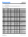
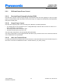
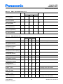
Table 5
Internal1 (1.5 V) Supplied Pins
Parameter
Values
Symbol
Unit
Note / Test Condition
Min.
Typ.
Max.
Input low voltage
-0.3
–
0.27
V
–
Input high voltage
1.15
–
3.6
V
–
Output low voltage
–
–
0.25
V
IOL = 1 mA
Output high voltage
1.1
–
–
V
IOH = -1 mA
–
–
1
mA
–
Pin Capacitance
–
–
10
pF
–
Magnitude Pin Leakage
–
0.01
1
μA
Input and output drivers
disabled
Continuous Load
1)
1) The totaled continuous load for all Internal1 supplied pins shall not exceed 2mA at the same time
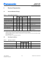
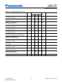
Table 6
Internal2 (2.5 V) Supplied Pins
Parameter
Values
Symbol
Unit
Note / Test Condition
Min.
Typ.
Max.
Input low voltage
-0.3
–
0.45
V
–
Input high voltage
1.93
–
2.8
V
P0.10
Input high voltage
1.93
–
3.6
V
Other pins
Output low voltage
–
–
0.25
V
IOL = 5 mA
Output low voltage
–
–
0.15
V
IOL = 2 mA
Output high voltage
2.0
–
–
V
IOH = -5 mA
Output high voltage
2.1
–
–
V
IOH = -2 mA
Continuous Load1)
–
–
5
mA
–
Pin Capacitance
–
–
10
pF
–
Magnitude Pin Leakage
–
0.01
1
μA
Input and output drivers
disabled
1) The totaled continuous load for all Internal2 supplied pins shall not exceed 35 mA at the same time
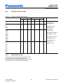
Table 7
VDDUART Supplied Pins
Parameter
Values
Symbol
Unit
Note / Test Condition
Min.
Typ.
Max.
Input low voltage
-0.3
–
0.2*VDDUART
V
–
Input high voltage
0.7*VDDUART –
VDDUART+0.3
V
P0.5/UARTRXD
Input high voltage
0.7*VDDUART –
3.6
V
Other pins
User’s Manual
Hardware Description
21
Revision 3.0, 2010-03-01