1
PAN1321-SPP
ENW89811J4CF
Assembly Guidelines
8.4
Assembly
8.4.1
Component Placement
In order to assure a high yield, good placement on the PCB is necessary. As a rule of thumb the tolerable
misplacement is 150 µm. This means that the PAN1321 module can be assembled with a variety of placement
systems.
It is recommended to use a vision system capable of package pad recognition and alignment that evaluates the
pad locations on the package (in contrast to outline centring). This eliminates the pad to package edge tolerance.
The recommendation is to pick and place the module with a nozzle in the centre of the shield. The nozzle diameter
shall not be bigger than 4 mm.
8.4.2
Pin Mark
1.00 mm
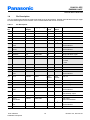
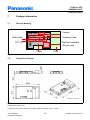
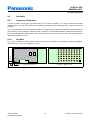
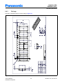
Pin 1 (A1) is marked on bottom footprint and on the top of the shield on the module according to Figure 9.
Diameter of pin 1 mark on the shield is 0.15 mm.
Pin 1
Ø150 µm
F9
F8
F7
F6
F5
F4
F3
F2
F1
E9
E8
E7
E6
E5
E4
E3
E2
E1
D9
D8
D7
D6
D5
D4
D3
D2
D1
C9
C8
C7
C6
C5
C4
C3
C2
C1
B9
B8
B7
B6
B5
B4
B3
B2
B1
A9
A8
A7
A6
A5
A4
A3
A2
A1
Pin 1
1,00 mm
Figure 9
Figure 2a: Top View
Figure 2b: Bottom View
Pin Marking
User’s Manual
Hardware Description
31
Revision 3.0, 2010-03-01