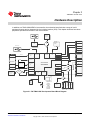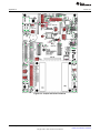
1
Tiva™ TM4C129X Development Board
User's Guide
Literature Number: SPMU360
October 2013
Contents
1
DK-TM4C129X Overview
1.1
1.2
1.3
1.4
2
Hardware Description
2.1
3
...................................................................................................... 4
Kit Contents ..................................................................................................................
Using the DK-TM4C129X ..................................................................................................
Features ......................................................................................................................
Specifications ................................................................................................................
5
5
5
6
.......................................................................................................... 7
Functional Description ...................................................................................................... 8
2.1.1 Microcontroller ...................................................................................................... 8
2.1.2 Clocking ............................................................................................................. 8
2.1.3 Reset ................................................................................................................ 8
2.1.4 Debugging and Programming .................................................................................... 8
2.1.5 Power ................................................................................................................ 9
2.1.6 USB Host/Device/OTG .......................................................................................... 10
2.1.7 User Buttons and User LED .................................................................................... 10
2.1.8 Headers ............................................................................................................ 11
2.1.9 Speaker ............................................................................................................ 14
2.1.10 EEPROM and SD Card ......................................................................................... 14
2.1.11 Temperature Sensor ............................................................................................ 15
2.1.12 LCD ............................................................................................................... 15
2.1.13 Ethernet ........................................................................................................... 17
2.1.14 Hibernation ....................................................................................................... 17
Software Development
....................................................................................................... 18
Software Description ......................................................................................................
Source Code ...............................................................................................................
Tool Options ................................................................................................................
Programming the DK-TM4C129X Board ...............................................................................
18
18
18
18
20
D
........................................................................................................
Bill of Materials (BOM) .......................................................................................................
References .......................................................................................................................
Schematics .......................................................................................................................
2
Contents
3.1
3.2
3.3
3.4
A
B
C
Component Locations
23
27
28
SPMU360 – October 2013
Submit Documentation Feedback
Copyright © 2013, Texas Instruments Incorporated
www.ti.com
List of Figures
1-1.
Board Picture ................................................................................................................
4
2-1.
DK-TM4C129X Development Board Block Diagram ...................................................................
7
2-2.
Booster Pack 1.............................................................................................................
11
2-3.
Booster Pack 2.............................................................................................................
12
2-4.
ULPI, MII, and RMII .......................................................................................................
13
2-5.
Resistive Touch Screen
..................................................................................................
16
2-6.
LCD Pin Out ................................................................................................................
16
A-1.
DK-TM4C129X Component Locations (Top View) ....................................................................
20
A-2.
DK-TM4C129X Component Locations (Bottom View) ................................................................
21
A-3.
Jumper and Shunt Locations
............................................................................................
22
List of Tables
1-1.
DK-TM4C129X Specifications .............................................................................................
2-1.
JTAG Pin Table .............................................................................................................
9
2-2.
USB Host/Device/OTG Signals ..........................................................................................
10
2-3.
User Buttons and LED Pins ..............................................................................................
10
2-4.
J28 ...........................................................................................................................
13
2-5.
J27 ...........................................................................................................................
14
2-6.
J34 ...........................................................................................................................
17
SPMU360 – October 2013
Submit Documentation Feedback
List of Figures
Copyright © 2013, Texas Instruments Incorporated
6
3
Chapter 1
SPMU360 – October 2013
DK-TM4C129X Overview
The Tiva TM4C129X development kit is an evaluation platform for the Tiva TM4C129x-series ARM®
Cortex™-M4-based microcontrollers. The evaluation board's design highlights the TM4C129X
microcontroller's USB 2.0 On-The-Go/Host/Device (OTG/Host/Device) interface, the 10BASE-T/100BASETX Ethernet controller with internal PHY, QuadSSI bus to communicate with an external flash device, 12bit Analog-to-Digital Converter (ADC), LCD controller, and the I2C module.
Quad SPI
512Mb Flash
BoosterPack2/EM
3.3V
UART 3 Jumper Regulator
Current
Measure
JTAG
Header
ICDI
Power LED
ICDI
Status
LED
USB microB
Debug/power
microSD
Card Slot
Power Select
Jumper
BoosterPack 2
I2C or SPI
Jumper
5V Barrel
Connector
Audio Amp
USB microAB
OTG
Speaker
Tiva C Series
TM4C129XNCAD
Microcontroller
Ethernet
LEDs
Ethernet
Connector
Reset
Button
Power
LEDs
Backlight
Jumper
Backlight
Driver
Up
Button
Tri-color
User
LED
Down
Button
Select
Button
Figure 1-1. Board Picture
All trademarks are the property of their respective owners.
4
DK-TM4C129X Overview
SPMU360 – October 2013
Submit Documentation Feedback
Copyright © 2013, Texas Instruments Incorporated
Kit Contents
www.ti.com
1.1
Kit Contents
The DK-TM4C129X Development Kit comes with the following:
• DK-TM4C129X development board
• On board In-Circuit Debug Interface (ICDI)
• Cables:
– Two USB Micro-B plug to USB-A plug cables
– USB Micro-A plug to USB-A receptacle cable
– Cat5 ethernet cable
• USB Flash drive containing:
– Complete documentation
– TivaWare™ for C Series Peripheral Driver Library and example source code
– A supported evaluation version of all of the following:
• Texas Instruments’ Code Composer Studio™ IDE
• Keil™ RealView® Microcontroller Development Kit (MDK-ARM)
• IAR Embedded Workbench® development tools
• Sourcery CodeBench™ development tools (time limited)
• GCC
1.2
Using the DK-TM4C129X
The recommended steps for using the DK-TM4C129X development kit are:
1. Follow the "Getting Stated Guide" document included in the kit. The Getting Started Guide
document will help get the DK-TM4C129X development board up and running in minutes.
2. Use your preferred ARM tool-chain and the Tiva Peripheral Driver Library to develop an
application. Software applications are loaded using the on-board In-Circuit Debug Interface (ICDI).
See Chapter 3, Software Development, for the programming procedure. The TivaWare Peripheral
Driver Library User's Guide contains specific information on software structure and function.
3. Customize and integrate the hardware to suit an end application. This user's manual is an
important reference for understanding circuit operation and completing hardware modification.
1.3
Features
The DK-TM4C129X development kit includes the following features:
• Tiva TM4C129X Microcontroller
– 32-bit ARM® Cortex™-M4F core
• QVGA color display with resistive touch screen
• 10BASE-T/100BASE-TX controller with internal PHY
• USB Micro-AB connector for Host/Device/OTG
• microSD card slot
• 3 navigation buttons
• User tricolor LED
• Precision 3.0V reference
• Quad SSI to 512 Mbit flash
• BoosterPack XL connector for expansion
• BoosterPack connector for expansion
• EM connector for wireless applications
• Available I/O brought out to headers on 0.1" grid
– ULPI USB external PHY (for high speed USB 2.0)
SPMU360 – October 2013
Submit Documentation Feedback
DK-TM4C129X Overview
Copyright © 2013, Texas Instruments Incorporated
5
Specifications
•
•
•
1.4
www.ti.com
– RMII and MII external Ethernet PHY
– EPI, Host bus 16/8
Debug
– Tiva In-Circuit Debug Interface (ICDI)
– Standard 20-pin JTAG header without ETM functionality (debug in and out capable)
Shunt resistors to measure current on VDDVBATVDDA and VREF to the TM4C129X
Reset button
Specifications
Table 1-1 shows the specifications for the DK-TM4C129X development board.
Table 1-1. DK-TM4C129X Specifications
Parameter
6
Value
Board supply voltage
4.75-5.25V
Dimensions
6.45" x 4.5" x 0.84" (LxWxH)
RoHS status
Compliant
DK-TM4C129X Overview
SPMU360 – October 2013
Submit Documentation Feedback
Copyright © 2013, Texas Instruments Incorporated
Chapter 2
SPMU360 – October 2013
Hardware Description
In addition to a TM4C129XNCZAD microcontroller, the evaluation board includes a range of useful
peripheral features and an integrated in-circuit debug interface (ICDI). This chapter describes how these
peripherals operate and interface to the microcontroller.
USB- Mini B
20 PIN JTAG
connector
SPI
ICDI
Logic
Use JTAG or
ICDI
Sd Card/ 512 Mbit
EEPROM
I2C
OTG- Micro A/B
UART
Diff pair
Booster Pack1
Analog
Timers
QSSI2
High speed USB PHY
USB High speed
MAC
USB ULPI
USB Full speed PHY
JTAG-UART0
QSSI3
SPI/could use quad-spi for higher speed
I2C3
UART5
MII/RMII
BoosterPack XL2
Ethernet MAC
SPI
Expansion Header
I2C
Texas Instruments
Ethernet w/LEDs
Ethernet PHY
Ethernet Internal
PHY
Booster Pack2
EPI Partial Host Bus
16/8
EPI
I2C7
Touch screen
Jumpers
Touch screen ADC
3 POS
JUMPER
UART3
LCD LIDD 8
QVGA LCD w/
Resistive Touch
Screen
UART
3 POS
JUMPER
QSSI0
TM4C129XNCZADI
I2C6
GPIO
Timer Pins
CAN0
CAN
Tri-color
SPI
I2C Temperature
Sensor
I2C
Magnetic
speaker
driven by
PWM
through
active low
pass filter
UART
LED
Up
Select
Down
Switches
EM Connetor
Temp.
Sensor
Jumper
Figure 2-1. DK-TM4C129X Development Board Block Diagram
SPMU360 – October 2013
Submit Documentation Feedback
Hardware Description
Copyright © 2013, Texas Instruments Incorporated
7
Functional Description
2.1
www.ti.com
Functional Description
2.1.1 Microcontroller
The Tiva TM4C129XNCZAD is an ARM® Cortex™-M4-based microcontroller with 1024-KB flash memory,
256-KB SRAM, 120-MHz operation, USB Host/Device/OTG, Ethernet Controller, Intergrated Ethernet
PHY, Hibernation module, and a wide range of other peripherals. See the TM4C129XNCZAD
microcontroller data sheet for complete device details.
Most of the microcontroller signals are routed to 0.1" pitch break-out pads and labeled with their GPIO
reference. An internal multiplexer allows different peripheral functions to be assigned to each of these
GPIO pads. When adding external circuitry, consideration should be given to the additional load on the
development board’s power rails. The Tiva PinMux Utility can be used to quickly develop pin assignments
and the code required to configure them.
The TM4C129XNCZAD microcontroller is factory-programmed with a quickstart weather display program.
The quickstart program resides in on-chip flash memory and runs each time power is applied, unless the
application has been replaced with a user program.
2.1.2 Clocking
The DK-TM4C129X uses a 25.0-MHz crystal (Y2) to complete the TM4C129XNCZAD microcontroller's
main internal clock circuit. An internal PLL, configured in software, can be used to multiply this clock to
higher frequencies for core and peripheral timing.
The Hibernation module is clocked off of an external 32.768 kHz crystal (Y3).
2.1.3 Reset
The RST signal into the TM4C129XNCZAD microcontroller connects to the RESET switch and to the ICDI
circuit for a debugger-controlled reset.
External reset is asserted (active low) under any one of these conditions:
• Power-on reset
• RESET switch held down
• By the ICDI circuit when instructed by the debugger (this capability is optional, and may not be
supported by all debuggers).
2.1.4 Debugging and Programming
•
•
8
ICDI: The DK-TM4C129X has a built in debugger, which can be used by connection to a computer
using the included USB micro-B to USB-A plug cable from the microUSB-B connector (J4) located in
the upper right of the board to a USB port on your computer. The on-board ICDI can also be used to
debug external boards using the ARM standard 20-pin connector (J1) and pulling all the shunts from
J3.
External debugger: an external debugger can be used through the ARM standard 20 pin connector J1.
Hardware Description
SPMU360 – October 2013
Submit Documentation Feedback
Copyright © 2013, Texas Instruments Incorporated
Functional Description
www.ti.com
Table 2-1. JTAG Pin Table
JTAG (J1) Pin
GPIO Pin (U1)
Pin Functions
Jumper J3 Pins
4
PC0
TCK
5, 6
2
PC1
TMS
3, 4
8
PC2
TDI
9, 10
6
PC3
TDO
7, 8
16
PA0
U0RX
13, 14
14
PA1
U0TX
15, 16
10
RESET
11, 12
18
TRST
N/A
1, 2
1
3.3V (with shunt)
3, 11, 15, 17, 19
GND
N/A
9
T_DISCONNECT
19, 20
5
EXTDBG (with shunt)
17, 18
12, 20
Reserved
EXTDBG is a signal that gets pulled low when attached to an external debugger. When pulled low, the
JTAG outputs of the ICDI controller are Z-stated.
T_DISCONNECT is a signal used to tell the ICDI when a device is connected to it.
J2 is a reserved jumper that may add functionality later. Leave unpopulated.
Note: The 20-pin connector (J1) is the ARM standard JTAG with ETM functionality connector. While the
TM4C129X devices support ETM functionality, this board does not have the necessary circuitry.
2.1.5 Power
The board is designed to be powered from one of two sources, they are selected by populating J11
jumper differently. The settings are as follows:
• Setting the shunt between pins 1 and 2 selects the barrel connector (J15) as the main 5-V source.
• Setting the shunt between pins 2 and 3 selects the ICDI USB (J4) as the power source.
J15 is a 6.5-mm diameter center power barrel connector. An example of a functional power supply is CUI
EMSA05300-P6P.
Power Jumper (J11) Options
Shunt on pin 1 and 2
Shunt on pin 2 and 3
Powered by J15
Powered by J4
The current and power consumption of the TM4C129X can be calculated by removing the shunt on J14
and measuring the voltage over the two pins, which are connected by a 1-Ω series resistor between the
pins. To calculate the current and power, use the following formulas:
ITM4C129X = VJ14 / 1Ω
PTM4C129X = VJ142 / 1Ω
(1)
(2)
The TPS62177DQC (U7) switching power regulator has many functions that are configured by omitting
resistors and including feedback to change the voltage on the 3.3-V rail. To learn more about these
features refer to the TPS62177DQC data sheet.
To power the external 3.3-V power supply without using the onboard voltage regulator (U7), remove the
shunt from J8 and connect 3.3-V directly to pin 1 of J8.
SPMU360 – October 2013
Submit Documentation Feedback
Hardware Description
Copyright © 2013, Texas Instruments Incorporated
9
Functional Description
www.ti.com
2.1.6 USB Host/Device/OTG
The DK-TM4C129X includes a USB Micro-AB (OTG) connector (J24) to allow for USB Host, Device, and
OTG operation. Table 2-2 shows the signals that are used for USB OTG:
Table 2-2. USB Host/Device/OTG Signals
GPIO Pin
Pin Function
USB OTG
PL6
USB0DP
D+
PL7
USB0DM
D-
PB0
USB0ID
ID
PB1
USB0VBUS
USB VBUS
Load Switch
PG4
USB0EPEN
USB VBUS Power Enable (EN)
PG5
USB0PFLT
Power Fault (OC)
In USB Host mode, the development board can provide power to the OTG connector. The USB0EPEN
signal controls the enable (EN) of a Texas Instruments’ TPS20511B Load Switch (U5), which enables
power to the connector's VBUS pin.
In Device mode, the development board can be powered from either the ICDI or the 5-V power supply.
In OTG mode, the USB controller is configured as Host or Device depending on the USB0ID signal and
the board is powered appropriately.
2.1.7 User Buttons and User LED
Three push buttons on the board provide navigation and selection for some of the example applications.
These buttons can be used for other purposes in the user’s custom applications.
The development board also has a tri-color user LED.
Table 2-3 shows how these features are connected to the pins on the microcontroller.
Table 2-3. User Buttons and LED Pins
10
Pin
Pin Function
Jumper
PP1
Select SW4
J37 pins 1 and 2
PN3
Up SW2
J37 pins 3 and 4
PE5
Down SW3
J37 pins 5 and 6
PN5
Red LED
J36 pins 1 and 2
PQ4
Blue LED
J36 pins 3 and 4
PQ7
Green LED
J36 pins 5 and 6
Hardware Description
SPMU360 – October 2013
Submit Documentation Feedback
Copyright © 2013, Texas Instruments Incorporated
Functional Description
www.ti.com
2.1.8 Headers
The three main sets of headers on the board are on a 0.100" grid and separated for a particular function.
2.1.8.1
BoosterPack 1
Figure 2-2 is a BoosterPack XL connection defined in the BoosterPack Design Guide. The port names and
voltage rails are listed in the silk screen next to the pin of the header.
AC
D B
1
0.10
0.90
0.10
10
1.80
Figure 2-2. Booster Pack 1
J29
CON A
Booster Function
J30
TM4C129X
Port
DK Function
CON B
Booster Function
TM4C129X
Port
DK Function
1
3.3V
N/A
GND
1
GND
N/A
2
Analog In
PE2
AIN01
2
Timer Output
PS2
3
UART RX
PH6
U5RX
3
INT. GPIO
PQ7
4
UART TX
PH7
U5TX
4
Test
N/A
NC
5
Int. GPIO
PN7
PN7
5
RESET
RESET
RESET
6
SPI A CLK
PF3
SSI3CLK
6
SPI_B_SIMO
PG5
SSI2XDAT0/
I2C3SDA
7
SPI B CLK
PG7
SSI2CLK
7
SPI_B_SOMI
PG4
SSI2DAT1/
I2C3CL
8
GPIO
PJ2
8
GPIO
PN0
PN0
9
GPIO
PB4
9
GPIO
PN1
PN1
10
GPIO
PJ7
10
GPIO
PN2
PN2
Booster Function
TM4C129X
Port
CON D
EM Function
TM4C129X
Port
DK Function
1
5V
N/A
1
Timer Output
PM5
T4CCP1
2
GND
2
Timer Output
PD3
T1CCP1
3
Analog IN
PE3
AIN00
3
Timer Output
PS3
T3CCP1
4
Analog IN
PE6
AIN20
4
Timer Output
PL5
T0CCP1
5
Analog IN
PK0
AIN16
5
Timer Output
PL4
T0CCP0
6
Analog IN
PK1
AIN17
6
Timer Output
PS0
T2CCP0
7
Analog IN
PK2
AIN18
7
Timer Output
PS1
T2CCP1
8
Analog IN
PK3
AIN19
8
Timer Output
PQ3
T7CCP1
9
Analog IN
PE0
AIN03
9
Timer Output
10
Analog IN
PE1
AIN02
10
Timer Output
CON C
DK Function
SPMU360 – October 2013
Submit Documentation Feedback
T3CCP0
NC
PM7
T5CCP1
Hardware Description
Copyright © 2013, Texas Instruments Incorporated
11
Functional Description
2.1.8.2
www.ti.com
BoosterPack 2
Figure 2-3 is a standard 20-pin BoosterPack (defined in the BoosterPack Design Guide). The port name,
functionality, and voltage rail are printed on the silk screen near the pin. For the BoosterPack 2 UART
port, the following jumpers must be set: J10 and J12 must have the shunts moved to pins 2 and 3 (this is
the side that says BOOSTER2 UART). For SPI, set jumpers J17 and J16 to pin 1 and 2, respectively; for
I2C, set jumpers 16 and 17 to pins 2 and 3.
A
B
0.10
0.90
1.80
Figure 2-3. Booster Pack 2
J6
12
J9
CON A
Booster Function
TM4C129X
DK Function
CON B
Booster
Function
TM4C129X
1
3.3V
N/A
GND
1
GND
N/A
2
Analog In
PD0
AIN15
2
Timer Output
PD1
3
UART RX
J12
Jumper
3
INT. GPIO
PQ0
DK Function
T0CCP0
4
UART TX
J13
Jumper
4
Test
N/A
NC
5
INT. GPIO
PQ1
PQ1
5
RESET
RESET
RESET
6
SPI A CLK
PF3
SSI3CLK
6
SPI_B_SIMO
J17/J16
Jumper
7
SPI B CLK
PA2
SSI0CLK
7
SPI_B_SOMI
J16/J17
Jumper
8
GPIO
PS6
8
GPIO
PQ2
PQ2
9
GPIO
PS7
9
GPIO
PN1
PP6
10
GPIO
PT0
10
GPIO
PN2
PT1
Hardware Description
SPMU360 – October 2013
Submit Documentation Feedback
Copyright © 2013, Texas Instruments Incorporated
Functional Description
www.ti.com
2.1.8.3
ULPI, MII, RMII, and EPI
There are two 16x2 headers on the left side of the board (J28 and J27). The majority of the J28 pins are
for MII and RMII signals, and the majority of J27 pins are for ULPI (an external USB PHY). Shared
between J28 and J27 are the connections for an EPI (host bus 16/8). There are also ground, +5V, +3.3V,
Hibernate and Wake pins mixed in with the connectors. Both headers are on a 100 mil grid.
J27
1
J28
2
1
2
0.10
31
32
31
32
0.50
Figure 2-4. ULPI, MII, and RMII
Table 2-4. J28
PIN
PORT
1
5V
FUNCTION
PIN
PORT
2
NC
3
PM6
EN0CRS
4
PF3
EN0MDIO
5
PF2
EN0MDC
6
PG7
EN0RXDV
7
PG2
EN0TXCLK
8
PA6
EN0RXCK/EPI0S8
9
GND
Ground
10
GND
11
PM4
EN0RREFCLK
12
PN6
13
PP0
EN0INTRN
14
3.3V
15
PQ5
EN0RXD0
16
PG3
EN0TXEN
17
PQ6
EN0RXD1
18
PG6
EN0RXER
19
PK5
EN0RXD2/EPI0S31/EN0LED2
20
PH0
EPI0S00
21
PK4
EN0RXD3/EPI0S32/EN0LED0
22
PH1
EPI0S01
23
PG4
EN0TXD0
24
PH2
EPI0S02
25
PG5
EN0TXD1
26
PH3
EPI0S03
27
PK6
EN0TXD2/EPI0S25/EN0LED1
28
PC7
EPI0S04
29
PK7
EN0TXD3/EPI0S24
30
PM7
EN0COL
31
GND
Ground
32
GND
SPMU360 – October 2013
Submit Documentation Feedback
FUNCTION
EN0TXER
Hardware Description
Copyright © 2013, Texas Instruments Incorporated
13
Functional Description
www.ti.com
Table 2-5. J27
PIN
PORT
1
5V
3
PB3
5
GND
7
PL1
9
PL0
11
FUNCTION
PIN
PORT
2
NC
USB0CLK/EPI0S28/EN0MDIO
FUNCTION
4
NC
6
3.3V
USB0D1/EPI0S17
8
PM3
EPI0S12
USB0D0/EPI0S16
10
PM2
EPI0S13
PL2
USB0D2/EPI0S18
12
PM1
EPI0S14
13
PL3
USB0D3/EPI0S19
14
PM0
EPI0S15
15
PL4
USB0D4/EPI0S26
16
PN4
EPI0S34
17
PL5
USB0D5/EPI0S23
18
PA7
EPI0S09
19
PP5
USB0D6
20
PC6
EPI0S05
21
PP4
USB0D7
22
PC5
EPI0S06
23
PP2
USB0NXT/EPI0S29
24
PC4
EPI0S07
25
PB2
USB0STP/EPI0S27
26
HIB
27
PP3
USB0DIR/EPI0S30
28
WAKE
29
PG1
EPI0S10
30
GND
31
PG0
EPI0S11
32
GND
2.1.9 Speaker
The speaker circuit is driven by the PWM coming from PB2(T5CCP0) to produce sound. The amplifier
(U6) is a Texas Instruments LM4819 and is turned on and off by PD4.
The circuit has two filters: a high-pass filter (C14 and R26) and a low-pass filter (C24 and R35). The highpass filter removes any DC bias and inaudible frequencies, which the low-pass filter removes the high
frequencies from the PWM pulses.
The amplifier is turned off by default; when PD4 is high the amplifier turns on, and when PD4 is low, the
amplifier turns off.
2.1.10 EEPROM and SD Card
Included on the development kit is a Macronix MX66L51235F 512 Mb EEPROM (U2) and a microSD card
slot (J5).
CAUTION
Do not hot plug the SD card, turn off power before adding or removing SD card!
To communicate with these memory devices, use SSI port 3. The EEPROM can use QUAD SSI or
standard SSI, while the SD card uses standard SSI.
14
Port
Function
Jumper J7 pins to shunt
PQ1
EEPROM Chip select
1 and 2
PQ0
SSI 3 Clock (used by EEPROM and SD card)
3 and 4
PQ2
SSI 3 Data 0 (EEPROM) or Data out (SD Card)
5 and 6
PF0
SSI 3 Data 1 (EEPROM) or Data in (SD Card)
7 and 8
PF4
SSI 3 Data 2
9 and 10
PF5
SSI 3 Data 4
11 and 12
PH4
SD card Chip Select
13 and 14
Hardware Description
SPMU360 – October 2013
Submit Documentation Feedback
Copyright © 2013, Texas Instruments Incorporated
Functional Description
www.ti.com
2.1.11 Temperature Sensor
The ambient temperature is measured by the Texas Instruments TMP100 temperature sensor (U4), which
is connected to the TM4C129X by I2C.
I2C module 6 is used to interface with the temperature sensor, which has a maximum resolution of 12 bits.
The TMP100 is accurate to +/- 2 °C within the range of -25 to +85 °C.
The initial value of the I2C slave address is 0b1001010 or 0x4A, code required to configure them. If the
default address conflicts with another device you have added to the I2C bus, the address can be changed
by populating or unpopulating resistors R29, R30, R24 and/or R25. Refer to the "Serial Bus Address"
section of the TMP100 datasheet for the various address settings.
There are 2.2-kΩ pull-up resistors on the SDA and SCL lines as required by the I2C specification. Refer to
the following table for connections to I2C temperature sensor:
Port
Function
Jumper to shunt
PB6
I2C6 SCL
J18
PB7
I2C6 SDA
J20
2.1.12 LCD
The DK-TM4C129X is equipped with a Kentec K350QVG-V2-F 320x240 RGB resistive touch screen that
is controlled by the LCD Controller of the TM4C129X MCU using the LCD Interface Display Driver (LIDD)
in 8-bit mode.
The backlight of the LCD is driven by a TI TPS61042 constant current supply (U9). The control line of U9
has multiple settings that are set by moving the shunt on J35.
Shunt Across
Effect
Pins 1 and 2 (default)
Always on
Pins 2 and 3
Backlight control is handled by PF1
(This pin is also used as an Ethernet LED; remove the shunt on pin 5 and 6 for jumper J33)
None
Always off
CAUTION
If the LCD is disconnected, remove the shunt, otherwise the U9 current
supply will get very hot and may be damaged.
The resistive touch screen works by reading one axis at a time. For example, to read the X-axis, set PE7
to high, PT2 to ground, and tri-state PT3. Then read the analog value of PP7. The higher the voltage, the
farther left the user is on the touch screen. To read the Y-axis, set PT3 to high, PP7 to ground, and tristate PT2. Then read the analog value of PE7. The higher the voltage, the higher the user is on the touch
screen. Refer to Figure 2-5.
SPMU360 – October 2013
Submit Documentation Feedback
Hardware Description
Copyright © 2013, Texas Instruments Incorporated
15
Functional Description
www.ti.com
PT3/YD
PT2/XL
PE7/XR
PP7/YU
Figure 2-5. Resistive Touch Screen
Note: The analog input PE7 (AIN21) is under commit control and extra steps are required in software to
enable the function of the pin to be changed, see the "Commit Control" section of the datasheet for more
information and the software steps required to enable proper operation of the touch screen.
J34 enables the use of another display or other uses of the LCD pins. There are mounting holes under the
LCD to facilitate the use and mounting of other displays (refer to Figure 2-6 for dimensions). If the default
LCD is used, the default shunts must be in place (shown in Figure A-3).
0.50
Ø 0.15x4
2.20
3.20
Figure 2-6. LCD Pin Out
16
Hardware Description
SPMU360 – October 2013
Submit Documentation Feedback
Copyright © 2013, Texas Instruments Incorporated
Functional Description
www.ti.com
Table 2-6. J34
PIN
PORT
FUNCTION
PIN
LCD PIN NAME
1
3
LCD FUNCTION
N/A
5V
2
N/A
5V
N/A
3.3V
4
N/A
3.3V
5
PE7
AIN21
6
XR
TOUCH ANALOG
7
PT2
GPIO
8
YD
TOUCH IO
9
PT3
GPIO
10
XL
TOUCH IO
11
PP7
AIN22
12
YU
TOUCH ANALOG
13
PF6
LCDMCLK
14
RST
SYSTEM RESET
15
PJ6
LCDAC
16
CS
CHIP SELECT
17
PR4
LCDDATA00
18
D1 & D10
LCD DATA
19
PR5
LCDDATA01
20
D2 & D11
LCD DATA
21
PF7
LCDDATA02
22
D3 & D12
LCD DATA
23
PR3
LCDDATA03
24
D4 & D13
LCD DATA
25
PR6
LCDDATA04
26
D5 & D14
LCD DATA
27
PR7
LCDDATA05
28
D6 & D15
LCD DATA
29
PS4
LCDDATA06
30
D7 & D16
LCD DATA
31
PS5
LCDDATA07
32
D8 & D17
LCD DATA
33
PR1
LCDFP
34
DC
PARALLEL INTERFACE
35
PR0
LCDCP
36
RD
READ SIGNAL
37
PR2
LCDLP
38
WR
WRITE SIGNAL
39
N/A
GND
40
N/A
GND
2.1.13 Ethernet
The DK-TM4C129X supports 10/100 Mbps Ethernet through J32. Each DK has been assigned a unique
MAC address that is stored in USER_REG0 and USER_REG1. The value of the MAC address can be
viewed on the Configuration display in the quickstart weather display example. J32 is driven from the
internal PHY of the TM4C129XNCZAD and the PHY controls three LED that indicate Link, Activity and
Speed. The pins used for the Ethernet LEDs can be used for other functions, but the shunts on jumper
J33 must be removed to enable alternative uses. Refer to the following table for pins:
Pin
Function
LED Color
Jumper
PK4
EN0LED0 (Link)
RED
J33, Pins 1 and 2
PK6
EN0LED1 (Activity)
GREEN
J33, Pins 3 and 4
PF1
EN0LED2 (Speed)
AMBER
J33, Pins 5 and 6
RBIAS
RBIAS
--
NO
EN0RXIN
EN0RXIN
--
NO
EN0RXIP
EN0RXIP
--
NO
EN0TXON
EN0TXON
--
NO
EN0TXOP
EN0TXOP
--
NO
Note: The pin controlling the Speed LED can be used to control the backlight for the LCD, refer to the
LCD section for information.
2.1.14 Hibernation
The DK-TM4C129X provides a 32.768-kHz crystal (Y3) as a clock source for the TM4C129X Hibernation
module. The board supports hibernation in VDD3ON mode. To measure the current draw during this
mode, see Section 2.1.5.
The sleep mode of the 3.3V regulator can be used by moving the 2.2-kΩ resistor from R2 to R16, which
enables the low power mode of the switcher (U7) when TM4C129XNCZAD (U1) goes into hibernation.
SPMU360 – October 2013
Submit Documentation Feedback
Hardware Description
Copyright © 2013, Texas Instruments Incorporated
17
Chapter 3
SPMU360 – October 2013
Software Development
This chapter provides general information on software development as well as instructions for flash
memory programming.
3.1
Software Description
The software provided with the DK-TM4C129X provides access to all of the peripheral devices supplied in
the design. The TivaWare™ for C Series Peripheral Driver Library is used to operate the on-chip
peripherals.
The software includes a set of example applications that use the TivaWare™ Peripheral Driver Library.
These applications demonstrate the capabilities of the TM4C129XNCZAD microcontroller, as well as
provide a starting point for the development of the applications for use on the DK-TM4C129X development
board.
3.2
Source Code
The complete source code is provided on the DK-TM4C129X USB flash drive. See the README First
document for a detailed description of hardware setup and how to install the source code. The source
code and binary files are installed in the TivaWare™ software tree.
3.3
Tool Options
The source code installation includes directories containing projects and makefiles for the following toolchains:
• Keil ARM RealView® Microcontroller Development System
• IAR Embedded Workbench for ARM
• Sourcery Codebench
• Generic GNU C Compiler
• Texas Instruments' Code Composer Studio™ IDE
Download evaluation versions of these tools from the Tools & Software section of www.ti.com/tiva. Due to
code size restrictions, the evaluation tools may not build all example programs. A full license is necessary
to re-build or debug all examples.
Instructions on installing and using each of the evaluation tools can be found in the Quickstart guides (for
example, in the Keil Quickstart or IAR Quickstart) in the References section of this document .
For detailed information on using the tools, see the documentation included in the tool chain installation or
visit the website of the tools supplier.
3.4
Programming the DK-TM4C129X Board
The DK-TM4C129X software package includes pre-built binaries for each of the example applications. If
you installed the TivaWare™ software to the default installation path of C:\ti\TivaWare_C_Series-x.x, you
can find the example applications in C:\ti\TivaWare_C_Series-x.x\examples\boards\dk-tm4c129x. The onboard ICDI is used with the LM Flash Programmer tool to program applications on the DK-TM4C129X
board.
Follow these steps to program example applications into the DK-TM4C129X development board using the
ICDI:
18
Software Development
SPMU360 – October 2013
Submit Documentation Feedback
Copyright © 2013, Texas Instruments Incorporated
Programming the DK-TM4C129X Board
www.ti.com
1. Install the Stellaris ICDI drivers on a Windows PC. Refer to the README First and the Stellaris Driver
Installation Guide.
2. Install LM Flash Programmer on the PC.
3. Connect the USB-A cable plug to an available port on the PC and the Mini-B plug to the board.
4. Verify that the power LEDs (D9, D10 and D1) on the board are lit.
5. Run LM Flash Programmer.
6. In the Configuration tab, use the Quick Set control to select the DK-TM4C129X development board.
7. Move to the Program tab and click the Browse button. Navigate to the example applications directory
(the default location is C:\ti\TivaWare_C_Series-x.x\examples\boards\dk-tm4c129x\).
8. Each example application has its own directory. Navigate to the example directory that you want to
load and then into the directory that contains the binary (*.bin) files. Select the binary file and click
Open.
9. Set the “Erase Method” to “Erase Necessary Pages,” check the “Verify After Program” box, and check
“Reset MCU After Program”.
10. Click the Program button to start the Erase, Download, and Verify process. The DEBUG ACTIVE LED
(D2) on the board turns on at this time.
Program execution starts once the Verify process is complete.
SPMU360 – October 2013
Submit Documentation Feedback
Software Development
Copyright © 2013, Texas Instruments Incorporated
19
Appendix A
SPMU360 – October 2013
Component Locations
Figure A-1. DK-TM4C129X Component Locations (Top View)
20
Component Locations
SPMU360 – October 2013
Submit Documentation Feedback
Copyright © 2013, Texas Instruments Incorporated
Appendix A
www.ti.com
Figure A-2. DK-TM4C129X Component Locations (Bottom View)
SPMU360 – October 2013
Submit Documentation Feedback
Component Locations
Copyright © 2013, Texas Instruments Incorporated
21
Appendix A
www.ti.com
Figure A-3. Jumper and Shunt Locations
22
Component Locations
SPMU360 – October 2013
Submit Documentation Feedback
Copyright © 2013, Texas Instruments Incorporated
Appendix B
SPMU360 – October 2013
Bill of Materials (BOM)
Item
Ref
Qty
Description
Mfg
Part Number
TDK
C1608X7R1H332K
1
C1, C30
2
Capacitor, 3300pF, 50V, 10%,
X7R, 0603
2
C12, C55
2
Capacitor, 2.2uF, 16V, 10%,
0603, X5R
Murata
GRM188R61C225KE15D
34
Capacitor, 0.1uF 50V, 20%
0603 X7R
TDK
C1608X7R1H104M
3
C13,
C33,
C40,
C62,
C71,
C16, C28, C29, C31,
C34, C35, C36, C37,
C42, C50, C52, C53,
C65, C66, C67, C68,
C72, C73, C74, C75,
C82, C83, C84, C86
C32,
C39,
C54,
C70,
C81,
4
C14
1
Capacitor, .047uF 16V 10%
X7R 0805
AVX
0805YC473KAT2A
5
C17, C19
2
Capacitor, 4.7uF, 6.3V, 10%
0805, X5R
Taiyo Yuden
JMK212BJ475KG-T
6
C2
1
Capacitor, 22uF 6.3V 20% X5R
0805
TDK
C2012X5R0J226M/1.25
7
C20
1
Capacitor, 0.47uF 10V 10%
X5R 0603
TDK
C1608X5R1A474K
8
C21
1
Capacitor, 1.0uF 25V 10% X5R
0603
TDK
C1608X5R1E105K
9
C24
1
Capacitor, 750pF, 50V, 10%,
0603, X7R
Samsung
CL10B751KB8NNNC
10
C26, C27
2
Capacitor, 12pF, 50V 5%, 0402,
COG
Murata
GRM1555C1H120JZ01D
11
C3, C6, C22, C45, C46, C56,
C60
7
Capacitor, 0.1uF 16V, 10%
0402 X7R
Taiyo Yuden
EMK105B7104KV-F
12
C38
1
Capacitor, 4700pF, 2kV, 10%,
X7R, 1812
AVX
1812GC472KAT1A
13
C4
1
Capacitor, 2.2uF 50V 10% X5R
0805
TDK
C2012X5R1H225K
14
C43
1
Capacitor, 4.7uF 10V 10% X5R
0603
TDK
C1608X5R1A475K/0.50
15
C5, C11, C18, C41, C57, C59,
C69, C76, C77, C78, C79, C80,
C85, C87
14
Capacitor, 1uF , X5R, 10V,
0402
TDK
C1005X5R1A105M050BB
16
C7, C47, C49, C58, C61, C63,
C64
7
Capacitor, 0.01uF 25V, 10%
0402 X7R
Taiyo Yuden
TMK105B7103KV-F
17
C8, C10, C23, C25
4
Capacitor, 10pF, 50V, 5%,
NPO/COG, 0402
Murata
GRM1555C1H100JZ01D
18
C9, C15, C44, C51
4
Capacitor, 0.1uF 50V, 10%
0603 X7R
Murata
GRM188R71H104KA93D
19
C90
1
Capacitor, 1000pF, 2kV, 20%,
X7R, 1812
Kemet
C1210C102MGRACTU
20
D1, D2, D10, D15
4
LED, Green 565nm, Clear 0805
SMD
Lite-On
LTST-C171GKT
21
D11
1
Diode,Schottky, 40V, 200mA
SOT-23
Fairchild
FYV0704SMTF
22
D12
1
LED, Tri-Color RGB, 0404 SMD
Common Anode
Lumex
SML-LX0404SIUPGUSB
SPMU360 – October 2013
Submit Documentation Feedback
Bill of Materials (BOM)
Copyright © 2013, Texas Instruments Incorporated
23
Appendix B
24
www.ti.com
Item
Ref
Qty
Description
Mfg
Part Number
23
D13
1
Diode, Schottky, 60V, 15ma,
SOD-323
Diodes Inc
SD101AWS-7-F
24
D14
1
Diode, 8 chan, +/-15KV, ESD
Protection Array, SO-8
Semtech
SLVU2.8-4.TBT
25
D16
1
LED, Red 630nm, Clear 0805
SMD
Lite-On
LTST-C171EKT
26
D3, D4, D5, D6, D7
5
Diode, 5.6V ESD Suppressor
0402
EPCOS
B72590D0050H160
27
D8, D9
2
LED AMBER CLEAR 0805
SMD
Lite-On
LTST-C170AKT
28
J1
1
Header, 2x10, 2.00mm, SMT,
Vertical, Unshrouded
Samtec
ASP17298501
29
J10
1
Header, 1x2, T-Hole Vertical
unshrouded stacking
Samtec
ZW-02-15-F-S-265-090
30
J11, J12, J13, J16, J17, J35
6
Header, 1x3, 0.100, T-Hole,
Vertical Unshrouded, 0.220
Mate
FCI
68001-103HLF
31
J15
1
Connector, DC Jack SMT
2.5x5.5mm
CUI Inc
PJ-002B-SMT
32
J19, J31
2
Header, 2x10, 0.050, SMT,
Vertical, Shrouded, Socket
Samtec
TFM-110-02-S-D-K-A
33
J2, J8, J14, J18, J20, J21, J22,
J23, J26
9
Header, 1x2, 0.100, T-Hole,
Vertical Unshrouded, 0.220
Mate
3M
961102-6404-AR
34
J24
1
Connector, USB micro AB
Receptacle Reversed SMD
Hirose
ZX62R-AB-5P
35
J25
1
Header, 2x4, 0.100, T-Hole,
Vertical Unshrouded, 0.230
Mate, gold
FCI
67997-108HLF
36
J27, J28
2
Header, 2x16, 0.100, T-Hole,
Vertical Unshrouded, 0.230
Mate, gold
FCI
67997-132HLF
37
J29, J30
2
Header, 2x10, T-Hole Vertical
unshrouded stacking
Samtec
ZW-10-15-F-D-265-090
38
J3
1
Header, 2x10, 0.100, T-Hole,
Vertical Unshrouded, 0.230
Mate, gold
FCI
67997-220HLF
39
J32
1
Connector, RJ45 NO MAG,
shielded THRU HOLE
TE Connectivity
1-406541-5
40
J33, J36, J37
3
Header, 2x3, 0.100, T-Hole,
Vertical Unshrouded, 0.230
Mate, gold
FCI
67996-206HLF
41
J34
1
Header, 2x20, 0.100, T-Hole,
Vertical Unshrouded, 0.230
Mate, gold
FCI
67997-240HLF
42
J39
1
Connector, FPC 60P, r/a
0.5mm pitch SMT
FCI
10085901-6015ELF
43
J4
1
Connector, rcpt, micro usb B
SMB
Hirose
ZX62-B-5PA
44
J5
1
Connector, Micro SD card,
push-push SMT
3M
2908-05WB-MG
45
J6, J9
2
Header, 1x10, T-Hole Vertical
unshrouded stacking
Samtec
ZW-10-15-F-S-265-090
46
J7
1
Header, 2x7, 0.100, T-Hole,
Vertical, Unshrouded, 0.230
Mate
FCI
67997-114HLF
47
K1
1
Speaker, 8 Ohm, 15mm diam,
0.5W, 87dB, SM
CUI Inc
CVS-1508
48
L1
1
Inductor 10uH, SMD
2.8x2.8mm, 0.5A, 0.47 Ohm
Wurth
744029100
Bill of Materials (BOM)
SPMU360 – October 2013
Submit Documentation Feedback
Copyright © 2013, Texas Instruments Incorporated
Appendix B
www.ti.com
Item
Ref
Qty
Description
Mfg
Part Number
49
L2
1
Inductor 6.8uH, SMD
4mmx4mm, 1.06A, 0.132 Ohm
Taiyo Yuden
NR4018T6R8M
50
Q1, Q2, Q3, Q4
4
NPN SC70 pre-biased
Diodes Inc
DTC114EET1G
Panasonic
ERJ-3GEYJ104V
51
R1
1
Resistor, 100K OHM 1/10W 5%
0603 Thick
52
R14
1
Resistor, 1K Ohm, 1/10W, 5%,
SMD, Thick
Panasonic
ERJ-3GEYJ102V
53
R18
1
Resistor, 5.6k ohm, 1/10W, 5%,
0402
Panasonic
ERJ-2GEJ562X
54
R19, R36
2
Resistor, 1M OHM 1/10W 5%
0603 SMD
Panasonic
ERJ-3GEYJ105V
55
R2, R23, R28
3
Resistor, 2.2K OHM 1/10W 5%
0603 SMD
Vishay
CRCW06032K20JNEA
56
R20
1
Resistor, 1 OHM 1/10W 1%
0603, Thick
Panasonic
ERJ-3RQF1R0V
57
R26, R35
2
Resistor, 20K OHM 1/10W 5%
0603 Thick
Yageo
RC0603JR-0720KL
58
R3, R10, R45, R46, R47
5
Resistor, 330 OHM 1/10W 5%
0603 SMD
Panasonic
ERJ-3GEYJ331V
59
R33
1
Resistor, 0 ohm, 1/10W, 5%,
0402
Panasonic
ERJ-2GE0R00X
60
R37, R40, R41, R42
4
Resistor, 49.9 OHM 1/10W 1%
0603 Thick
Panasonic
ERJ-3EKF49R9V
61
R38
1
Resistor, 4.87K Ohm, 1/10W,
1%, SMD, Thick
Panasonic
ERJ-3EKF4871V
62
R44
1
RES 1M OHM 5% 1206 TF
Panasonic
ERJ-8GEYJ105V
63
R48, R49
2
Resistor, 330 ohm, 1/10W, 5%,
0402
Yageo
RC0402FR-07330RL
64
R5, R24, R29, R31, R32, R43,
R51, R52, R53, R54, R58, R59,
R60, R62
14
Resistor, 10K OHM 1/10W 5%
0603 SMD
Panasonic
ERJ-3GEYJ103V
65
R50
1
Resistor, 13.0 OHM 1/10W 1%
0603 Thick
Panasonic
ERJ-3EKF13R0V
66
R55, R56, R57
3
Resistor, 1.2k ohm, 1/10W, 5%,
0402
Panasonic
ERJ-2GEJ122X
67
R6
1
Resistor, 33 ohm, 1/10W, 5%,
0402
Panasonic
ERJ-2GEJ330X
68
R63
1
Resistor, 51 ohm, 1/10W, 5%,
0402
Panasonic
ERJ-2GEJ510X
69
R64, R65, R66, R67
4
Resistor, 75 Ohm, 1/10W, 1%,
SMD, Thick
Panasonic
ERJ-3EKF75R0V
70
R7, R11, R12, R13, R17, R21,
R22, R27, R34, R39, R61
11
Resistor, 10k ohm, 1/10W, 5%,
0402 Thick Film
Yageo
RC0402FR-0710KL
71
R8
1
Resistor, 0 OHM 1/10W 0603
SMD
Panasonic
ERJ-3GEY0R00V
72
SW1, SW2, SW3, SW4
4
Switch, Tact 6mm SMT, 160gf
Omron
B3S-1000
Pulse Electronics
HX1188NL
73
T1
1
Transformer, ethernet, 1 to 1.
SOIC 16
74
TL1, TL2, TL3, TL4, TL5, TL6
6
Terminal, Test Point Miniature
Loop, Red, T-Hole
Keystone
5000
75
U1
1
Stellaris MCU
TM4C129XNCZAD 212 BGA,
super
Texas Instruments
TM4C129XNCZAD
76
U2
1
Serial Flash 512Mbit 3.3V
WSON-8
Macronix
MX66L51235FZ2I-10G
77
U3
1
Stellaris TIVA MCU
TM4C123GH6PMI
Texas Instruments
TM4C123GH6PMI
SPMU360 – October 2013
Submit Documentation Feedback
Bill of Materials (BOM)
Copyright © 2013, Texas Instruments Incorporated
25
Appendix B
www.ti.com
Item
Ref
Qty
Description
Mfg
Part Number
78
U4
1
IC, Digital Temperature Sensor
-55C to +125C, +/-3C, SOT23-6
Texas Instruments
TMP100NA
79
U5
1
Load Switch, 5.5V, SOT23-5,
TPS2051BDBV
Texas Instruments
TPS2051BDBVT
80
U6
1
Op Amp, 0.35W AUDIO MONO
AB, 8TSSOP
Texas Instruments
LM4819MM
81
U7
1
Regulator, Step Down 3.3V,
0.5A
Texas Instruments
TPS62177DQC
82
U8
1
Precision 3.0V reference MSOP
Texas Instruments
REF3230AIDBVT
Texas Instruments
TPS61042DRBR
83
U9
1
White LED Driver IC 30V 1.5A
SOT23-5
84
Y1
1
Crystal, 16.00MHz 5.0x3.2mm
SMT
NDK
NX5032GA-16.000000MHZ
85
Y2
1
Crystal, 25.00MHz 5.0x3.2mm
SMT
NDK
NX5032GA-25.000000MHZ
86
Y3
1
Crystal, 32.768KHz Radial Can
Citizen Finetech
Miyota
CMR200T-32.768KDZY-UT
87
ZZ
1
BOARD,Snowflake
Development Kit Rev 2.0
PCB Do Not Populate List (Shown for information only)
88
C48
1
Capacitor, 0.1uF 16V, 10%
0402 X7R
Taiyo Yuden
EMK105B7104KV-F
89
R25, R30
2
Resistor, 10K OHM 1/10W 5%
0603 SMD
Panasonic
ERJ-3GEYJ103V
90
R4, R9, R15, R16
4
Resistor, No Value 1/10W 5%
0603 SMD
Anyone
R0603-OMIT
91
6
Rubber Feet, Adhesive, Round,
0.312 x 0.200
3M
SJ-61A1
92
58
Jumper, 0.100, Gold, Black,
Open
3M
969102-0000-DA
93
1
LCD Module 320 x 240 3.5"
TFT, 4-wire touch, White LED
Kentec
K350QVG-V2-F
94
4
VHB Double-Sided Foam Tape,
0.012"x0.5"x1.0"
3M
1/2-5-4926
Final Assembly Bill Of Materials
26
Bill of Materials (BOM)
SPMU360 – October 2013
Submit Documentation Feedback
Copyright © 2013, Texas Instruments Incorporated
Appendix C
SPMU360 – October 2013
References
In addition to this document, the following references are included on the Tiva TM4C123GH6PGE
Development Kit USB flash drive and are also available for download at www.ti.com.
• TivaWare Driver Library
• TivaWare Driver Library User’s Guide (SPMU298)
• README First (SPMU359)
• Getting Started Guide (SPMU361)
• Quick Start Guides:
– Tiva™ C Series Development and Evaluation Kits for Code Composer Studio™ (SPMU352)
– Tiva™ C Series Development and Evaluation Kits for Keil™ RealView® MDK (SPMU355)
– Tiva™ C Series Development and Evaluation Kits for IAR Embedded Workbench® (SPMU354)
– Tiva™ C Series Development and Evaluation Kits for Sourcery CodeBench™ Development Tools
(SPMU356)
• Stellaris Driver Installation Guide (SPMU287)
Information on development tool being used:
• RealView MDK website at www.keil.com/arm/rvmdkkit.asp
• IAR Embedded Workbench website at www.iar.com
• Sourcery CodeBench development tools website at www.codesourcery.com/gnu_toolchains/arm
• Texas Instruments’ Code Composer Studio™ IDE website at www.ti.com/ccs
SPMU360 – October 2013
Submit Documentation Feedback
References
Copyright © 2013, Texas Instruments Incorporated
27
Appendix D
SPMU360 – October 2013
Schematics
This section contains the schematics for the DK-TM4C129X board.
• Microcontroller, crystals and decoupling capacitors, page 1
• Ethernet, USB, and MII/RMII, ULPI and EPI headers, page 2
• SD card solt, SPI flash, temperature sensor, and speaker with amplifier, page 3
• BoosterPack headers and EM connectors, page 4
• LCD backlight driver, VREF regulator, 3.3V and 5V voltage sources, page 5
• LCD headers, LCD connector, Power LEDs, user LEDs, and user buttons, page 6
• Debug headers, debug jumpers, and ICDI microcontroler, page 7
28
Schematics
SPMU360 – October 2013
Submit Documentation Feedback
Copyright © 2013, Texas Instruments Incorporated
3.3V
3.3V
JTAG/DEBUG
FLASH_BUS
DEBUG_RX
DEBUG_TX
TCK
TMS
TDI
TDO
PQ1/SSI3SS
PQ0/SSI3CLK
PQ2/SSI3XDAT0
PF0/SSI3DAT1
PF4/SSI3DAT2
PF5//SSI3DAT3
PH4
V3
W3
B15
C15
D14
C14
E2
E3
H4
U6
V7
W7
R3
PF3/EN0MDIO/SSI3CLK
PG7/EN0RXDV
PG6/EN0RXER
PG2/EN0TXCK
PG3/EN0TXEN
PN6/EN0TXER
PP0/EN0INTRN
PM7/T5CCP1/EN0COL
PM6/EN0CRS
PQ5/EN0RXD0
PQ6/EN0RXD1
PK5/EN0RXD2/EPI0S31
PK4/EN0RXD3
PM4/EN0RREF_CLK
PG4/I2C3SCL/EN0TXD0
PG5/I2C3SDA/EN0TXD1
PK6/EN0TXD2/EPI0S25
PK7/EN0TXD3/EPI0S24
PF2/EN0MDC
PF1/TRD1/ENLED2
PA0/U0RX
PA1/U0TX
PC0/TCK/SWDCLK
PC1/TMS/SWDIO
PC2/TDI
PC3/TDO/SWO
PQ1/SSI3FSS
PQ0/SSI3CLK
PQ2/SSI3XDAT0
PF0/SSI3XDAT1
PF4/SSI3XDAT2
PF5/SSI3XDAT3
PH4
PK0/AIN16
PK1/AIN17
PK2/AIN18
PK3/AIN19
PQ4
PN5
PJ2
PJ3
PJ7
PN7
PN0
PN1
PN2
PH6/U5RX
PH7/U5TX
PM5/T4CCP1
PS0/T2CCP0
PS1/T2CCP1
T3CCP0/PS2
T3CCP1/PS3
PQ3/T7CCP1
PD2/T1CCP0/AIN13
PD3/T1CCP1/AIN12
T5CCP0/USB0STP/PB2
AIN20/PE6
PQ7
PE0/AIN3
PE1/AIN2
PE2/AIN1
PE3/AIN0
BUTTONS
SEL
UP
DOWN
Speaker
PD4/T3CCP0
PD5
PH5
PJ0/U3RX
PJ1/U3TX
PA2/SSI0CLK
PA3/SSI0FSS
PA4/SSI0XDAT0/SCL
PA5/SSI0XDAT1/SDA
PB4
PB5
Booster Pack 2
PC5/EPI0S06
32K
J23
EPI
PS6
PS7
PT0
PT1
PP6
PD0/AIN15
PD1/T0CCP0
PE4
PJ4/U3RTS
PJ5/U3CTS
PB6/I2C6SCL
PB7/I2C6SDA
PH0/EPI0S00
PH1/EPI0S01
PH2/EPI0S02
PH3/EPI0S03
PC7/EPI0S04
PC6/EPI0S05
PC4/EPI0S07
PA6/EN0RXCK/EPI0S08
PA7/EPI0S09
PG1/EPI0S10
PG0/EPI0S11
PM3/EPI0S12
PM2/EPI0S13
PM1/EPI0S14
PM0/EPI0S15
PP3/USB0DIR
PN4/EPI0S34
D7
B10
B5
A4
B4
T2
C8
E7
T6
U5
V4
W4
C6
B6
U10
R13
W10
V10
B8
C2
C1
A5
F18
E17
F2
F1
P4
R2
R1
T1
K3
L2
M1
M2
V5
R7
T14
N15
L19
L18
K19
K18
C12
A10
PP1
PN3
PE5/SSI1XDAT1
SSI1XDAT2/PD4
PD5/SSI1XDAT3
PH5
PJ0/U3RX
PJ1/U3TX
PA2/SSI0CLK
PA3/SSI0FSS
PA4/SSI0XDAT0
PA5/SSI0XDAT1
PB4/SSI1FSS
PB5/SSI1CLK
PS6
PS7
PT0
PT1
PP6/AIN23
PD0/AIN15
PD1/T0CCP0/AIN14
SSI1XDAT0/PE4
PJ4/U3RTS
PJ5/U3CTS
PB6/I2C6SCL
PB7/I2C6SDA
PB3/USB0CLK
PL0/USB0D0
PL1/USB0D1
PL2/USB0D2
PL3/USB0D3
PL4/USB0D4
PL5/USB0D5/EPI0S33
USB0D6/PP5
PP4/USB0D7
USB0NXT/PP2
PL6/USB0DP
PL7/USB0DM
USB0VBUS/PB1
USB0ID/PB0
PD6/USB0EPEN/AIN5
PD7/USB0PFLT/AIN4
PH0/EPI0S00
PH1/EPI0S01
PH2/EPI0S02
PH3/EPI0S03
PC7/EPI0S04
PC6/EPI0S05
PC5/EPI0S06
PC4/EPI0S07
PA6/EN0RXCK/EPI0S08
PA7/EPI0S09
PG1/EPI0S10
PG0/EPI0S11
PM3/EPI0S12
PM2/EPI0S13
PM1/EPI0S14
PM0/EPI0S15
PP3/EPI0S30/USBDIR
PT2
PT3
PE7/AIN21
PP7/AIN22
PF6/LCDMCLK
PR0/LCDCP
PR1/LCDFP
PR2/LCDLP
PJ6/LCDAC
PR4/LCDDATA00
PR5/LCDDATA01
PF7/LCDDATA02
PR3/LCDDATA03
PR6/LCDDATA04
PR7/LCDDATA05
PS4/LCDDATA06
PS5/LCDDATA07
EPI0S34/PN4
TM4C129X
T7
U14
V12
V11
M16
T12
D6
N18
N19
W12
U15
V17
U19
M18
K17
K15
V16
W16
W6
V6
PF3/SSI3CLK
PG7/SSI2CLK
PG6/EN0RXER
PG2/EN0TXCK
PG3/EN0TXEN
PN6/EN0TXER
PP0/EN0INTRN
PM7/T5CCP1/EN0COL
PM6/EN0CRS
PQ5/EN0RXD0
PQ6/EN0RXD1
PK5/EN0RXD2/EPI0S31
PK4/EN0RXD3/LED0
PM4/EN0RREF_CLK
PG4/SSIXDAT1
PG5/SSI2XDAT0
PK6/EN0TXD2/LED1
PK7/EN0TXD3
PF2/EN0MDC
PF1/LED2
J1
J2
K1
K2
A13
B9
H17
F16
K5
U12
C10
B11
A11
U2
V2
G15
D12
D13
B14
A14
M4
D2
D1
A17
A7
M3
H3
H2
G1
G2
PK0/AIN16
PK1/AIN17
PK2/AIN18
PK3/AIN19
PQ4/LED_B
PN5/LED_R
PJ2
PJ3
PJ7
PN7
PN0
PN1
PN2
PH6/U5RX
PH7/U5TX
PM5/T4CCP1
PS0/T2CCP0
PS1/T2CCP1
PS2/T3CCP0
PS3/T3CCP1
PQ3/T7CCP1
PD2/T1CCP0
PD3/T1CCP1
PB2/USB0STP
PE6/AIN20
PQ7/LED_G
PE0/AIN03
PE1/AIN02
PE2/AIN01
PE3/AIN00
B17
G16
H19
G18
J18
H18
G19
B12
D8
B13
PB3/USB0CLK
PL0/USB0D0
PL1/USB0D1
PL2/USB0D2
PL3/USB0D3
PL4/T0CCP0/USB0D4
PL5/T0CCP1/USB0D5/EPI0S33
PP5/USB0D6
PP4/USB0D7
PP2/USB0NXT
NOTE: To guarantee risetime requirements
MII/RMII
External Ethernet PHY
TOUCH0
TOUCH1
TOUCH_AN0
TOUCH_AN1
LCDCLK
LCDCP
LCDFP
LCDLP
LCDAC
LCDDATA00
LCDDATA01
LCDDATA02
LCDDATA03
LCDDATA04
LCDDATA05
LCDDATA06
LCDDATA07
C70
U1-B
P18
RESET
RESET
VBAT
P19
0.1uF
R39
10K
Y3
32.768Khz
C27
12pF
C26
12pF
XOSC0 T18
XOSC1 T19
GNDX R18
XOSC0
XOSC1
GNDX
MOSC0 E19
MOSC1 D19
OSC0
OSC1
GNDX2 D18
GNDX2
HIB
WAKE
VREFA+
VREFA-
M17
U18
WAKE
F4
G5
C18
1uF
R33
C59
1uF
0
3.3V
G4
C25
10pF
C58
0.01 uF
F3
C60
0.01UF
Y2
25MHz
3.0_VREF+
HIB
3.3V
VDDA
C23
10pF
L8
L9
M8
M9
N10
V1
W1
W2
M10
K10
K13
K14
K6
K9
F10
J11
J12
H10
H11
H12
A1
A18
A19
A2
B1
B19
Booster Pack 1
ULPI USB
GNDA
VDD
VDD
VDD
VDD
VDD
VDD
VDD
VDD
VDD
VDD
VDD
VDD
VDD
VDD
VDD
GND
GND
GND
GND
GND
GND
GND
GND
GND
GND
GND
GND
GND
GND
GND
GND
GND
GND
GND
GND
GND
GND
GND
GND
GND
GND
NC
NC
NC
NC
NC
NC
VDDC
VDDC
L10
L11
J8
J9
L12
M11
M12
P10
K11
K12
K7
K8
G10
H9
J10
C33
0.1uF
REVISION
3.0
C63
C64
0.1uF
0.01uF
0.01uF
C22
C56
0.1uF 0.1uF
3.3V
C29
C28
0.1uF
0.1uF
C52
C16
0.1uF 0.1uF
C39
C54
0.1uF
0.1uF
VDDC
H16
E10
C57
1uF
SLJ
C67
V18
V19
W18
W19
E13
C5
TM4C129X
DESIGNER
DATE
C53
C61
0.1uF
0.01 uF
C55
2.2 uF
TEXAS INSTRUMENTS
8/6/2013
TIVA C SERIES MICROCONTROLLERS
PROJECT
TM4C129X Development Kit
108 WILD BASIN ROAD, SUITE 350
AUSTIN TX, 78746
DESCRIPTION
LCDBUS
51
R63
VBAT
R34
10K
C18 USB0DP
B18 USB0DM
B16USB0VBUS USB_OTG
A16
USB0ID
B3 USB0EPEN
B2 USB0PLFT
E18
F17
B7
A8
T8
N5
N4
N2
N1
P3
P2
U8
V8
W9
R10
V9
T13
J26
U1-A
www.ti.com/tiva-c
Schematic, DK-TM4C129X
C-SERIES
FILENAME
DK-TM4C129X_3.0.sch
PART NO.
DK-TM4C129X
SHEET
1 OF 7
LED2
NOTE: Pull up resistors and decoupling cap should be located near U1
1
3
5
PK4/EN0RXD3/LED0
PK6/EN0TXD2/LED1
PF1/LED2
J33
LED1
LED0
LED1
LED2
SPEED(AMBER)
330
Amber
3.3V
3.3V
2
4
6
R45
D8
D15
R47
330
ACTIVITY(GREEN)
R46
330
LINK(RED)
Green
CON-HDR-2X3-0100
C65
C62
0.1uF
R42
R41
R40
LED0
0.1uF
R37
D16
RED
3.3V
49.9
U1-C
EN0TXOP
V15 EN0TX+
49.9
49.9
49.9
T1
3.3V
EN0TXON
P17
N16
EN0RXIP
VDD
VDD
R17
P16
V14 EN0TXW13 EN0RX+
3.3V
EN0RXIN
GND
GND
RBIAS
R65
R64
W15
4.87K
1%
R38
16
15
14
11
10
9
HX1188NL
V13 EN0RX-
TM4C129X
D14
1
2
3
6
7
8
C40
C66
0.1uF
0.1uF
75
J32
1
8
2
3
7
6
4
5
TX+_RJ45
TX-_RJ45
RX+_RJ45
RX-_RJ45
SLVU2.8-4
1
2
3
4
5
6
7
8
TX+
TXRX+
TERM1A
TERM1B
RXTERM2A
TERM2B
CHASIS
CHASIS
10
9
RJ45_NOMAG_NOLED
75
R66
R67
75
75
R44
C90
1000pF
C38
4700 pF
1M
NOTE: C40 and C66 must be located near pin 2 and 7 of T1
C30
3300pF
J24
R36
CON-USB-MICROAB-REV
ID
G
1M
9
8
5
D+
4
2
D-
3
VB
1
7
6
EPI_HOST_BUS16/8
+5V
+5V
3.3V_MAIN
+VBUS
MII/RMII
+5V
D6
C17
D5
4.7UF 6.3V
C19
4.7UF 6.3V
4
R31
10K
2
VIN
EN
OUT
OC
1
3
GND
+VBUS
USB_EN
USB_PLFT
1
3
5
7
2
4
6
8
J25
TPS2051B
USB0DM
USB0ID
USB0VBUS
USB0EPEN
USB0PLFT
USB_OTG
USB0DP
U5
USB_EN
C31
0.1uF
D7
5
PM6/EN0CRS
PF2/EN0MDC
PG2/EN0TXCK
PM4/EN0RREF_CLK
PP0/EN0INTRN
PQ5/EN0RXD0
PQ6/EN0RXD1
PK5/EN0RXD2/EPI0S31
PK4/EN0RXD3/LED0
PG4/SSIXDAT1
PG5/SSI2XDAT0
PK6/EN0TXD2/LED1
PK7/EN0TXD3
1
3
5
7
9
11
13
15
17
19
21
23
25
27
29
31
R27
10K
C34
0.1uF
J27
2
4
6
8
10
12
14
16
18
20
22
24
26
28
30
32
HDR-2X16-0100
3.3V_MAIN
ULPI_USB
J28
3.3V_MAIN
PF3/SSI3CLK
PG7/SSI2CLK
PA6/EN0RXCK/EPI0S08
PB3/USB0CLK
C32
0.1uF
PL1/USB0D1
PL0/USB0D0
PL2/USB0D2
PL3/USB0D3
PL4/T0CCP0/USB0D4
PL5/T0CCP1/USB0D5/EPI0S33
PP5/USB0D6
PP4/USB0D7
PP2/USB0NXT
PB2/USB0STP
PP3/USB0DIR
PG1/EPI0S10
PG0/EPI0S11
PN6/EN0TXER
PG3/EN0TXEN
PG6/EN0RXER
PH0/EPI0S00
PH1/EPI0S01
PH2/EPI0S02
PH3/EPI0S03
PC7/EPI0S04
PM7/T5CCP1/EN0COL
1
3
5
7
9
11
13
15
17
19
21
23
25
27
29
31
C15
0.1uF
2
4
6
8
10
12
14
16
18
20
22
24
26
28
30
32
PM3/EPI0S12
PM2/EPI0S13
PM1/EPI0S14
PM0/EPI0S15
PN4/EPI0S34
PA7/EPI0S09
PC6/EPI0S05
PC5/EPI0S06
PC4/EPI0S07
HIB
WAKE
C81
0.1uF
HDR-2X16-0100
C82
0.1uF
3.3V_MAIN
3.3V_MAIN
DESIGNER
SLJ
REVISION
3.0
DATE
TEXAS INSTRUMENTS
8/6/2013
TIVA C SERIES MICROCONTROLLERS
PROJECT
TM4C129X Development Kit
108 WILD BASIN ROAD, SUITE 350
AUSTIN TX, 78746
DESCRIPTION
www.ti.com/tiva-c
Schematic, DK-TM4C129X
C-SERIES
FILENAME
DK-TM4C129X_3.0.sch
PART NO.
DK-TM4C129X
SHEET
2 OF 7
3.3V_MAIN
3.3V_MAIN
R5
+5V
CS
SIO1
SIO2
GND
VCC
SIO3
SCLK
SIO0
8
7
6
5
U6
C14
J21
R26
PB2/USB0STP
J7
FLASH_BUS
1
3
5
7
9
11
13
20K
0.047uF
2
4
6
8
10
12
14
3.3V_MAIN
FLASH_CLK
FLASH_DAT0
FLASH_DAT1
FLASH_DAT2
FLASH_DAT3
SD_CS
3.3V_MAIN
J5
R59
10K
microSD CARD INTERFACE
CON-HDR-100-2X7-TH
3.3V_MAIN
NC1
CS
DI
VDD
CLK
VSS
DO
RSV
VO-
VDD/2
BYPASS
SD
5
2
8
1
VO+
+
GND
K1
R32
10K
C51
0.1UF
C
J22
PD4/T3CCP0
Q1
DTC114EET1G
B
9
10
11
12
R58
10K
-IN
+IN
0.47uF
X1
X2
X3
X4
1
2
3
4
5
6
7
8
4
3
LM4819
C20
CVS-1508
VDD
2
1
+5V
R60
10K
C21
1.0uF
MX66L5
PQ1/SSI3SS
PQ0/SSI3CLK
PQ2/SSI3XDAT0
PF0/SSI3DAT1
PF4/SSI3DAT2
PF5//SSI3DAT3
PH4
20K
R35
750 pF
FLASH_DAT3
FLASH_CLK
FLASH_DAT0
6
1
2
3
4
C24
C37
0.1UF
U2
7
10K
E
PB6/I2C6SCL
3.3V_MAIN
3.3V_MAIN
PB7/I2C6SDA
3.3V_MAIN
R23
2.2K
J20
J18
R28
R24
10K
2.2K
R30
10K
OMIT
3.3V_MAIN
1
2
3
U4
SCL
SDA
GND ADD0
ADD1 VDD
6
5
4
C9
0.1UF
TMP100
R29
10K
C44
0.1UF
R25
10K
OMIT
DESIGNER
SLJ
REVISION
3.0
DATE
TEXAS INSTRUMENTS
8/6/2013
TIVA C SERIES MICROCONTROLLERS
PROJECT
TM4C129X Development Kit
108 WILD BASIN ROAD, SUITE 350
AUSTIN TX, 78746
DESCRIPTION
www.ti.com/tiva-c
Schematic, DK-TM4C129X
C-SERIES
FILENAME
DK-TM4C129X_3.0.sch
PART NO.
DK-TM4C129X
SHEET
3 OF 7
3.3V_MAIN
+5V
3.3V_MAIN
A
A1
A2
A3
A4
A5
A6
A7
A8
A9
A10
PE2/AIN01
PH6/U5RX
PH7/U5TX
PN7
PF3/SSI3CLK
PG7/SSI2CLK
PJ2
PB4
PJ7
C1
C2
C3
C4
C5
C6
C7
C8
C9
C10
C71
PE3/AIN00
PE6/AIN20
PK0/AIN16
PK1/AIN17
PK2/AIN18
PK3/AIN19
PE0/AIN03
PE1/AIN02
C
D
EM_TX
EM_RX
PB7/I2C6SDA
PB6/I2C6SCL
+5V
C72
B1
B2
B3
B4
B5
B6
B7
B8
B9
B10
J19
1uF
PJ4/U3RTS
32K
J30
PM5/T4CCP1
PD3/T1CCP1
PS3/T3CCP1
PL5/T0CCP1/USB0D5/EPI0S33
PL4/T0CCP0/USB0D4
PS0/T2CCP0
PS1/T2CCP1
PQ3/T7CCP1
PD2/T1CCP0
PM7/T5CCP1/EN0COL
C77
0.1uF
2X10_BOOSTER_XL_1
D1
D2
D3
D4
D5
D6
D7
D8
D9
D10
3.3V_MAIN
EM_Connectors
J29
C78
0.1uF
PS2/T3CCP0
PQ7/LED_G
1uF
PD2/T1CCP0
PD3/T1CCP1
PA3/SSI0FSS
PA2/SSI0CLK
PA4/SSI0XDAT0/SCL
PA5/SSI0XDAT1/SDA
RESET
PG5/SSI2XDAT0
PG4/SSIXDAT1
PN0
PN1
PN2
1
3
5
7
9
11
13
15
17
19
2
4
6
8
10
12
14
16
18
20
J31
VSS
RF_UART_CTS
RF_SLOW_CLK(32K)
RF_UART_RX
RF_UART_TX
RF_I2C_SDA
RF_I2C_SCL
RF_SDIO_CLK
RF_SDIO_CMD
VSS
RF_SDIO_D0
RF_SDIO_D1
RF_SDIO_D2
RF_SDIO_D3
RF_GPIO0-GDO0
RF_GPIO1-GDO2
RF_SPI_CSn
RF_SPI_CLK
RF_SPI_MOSI
RF_SPI_MISO
VDD2(1.8V)OPTION
VDD2(1.8V)OPTION
VDD2(1.8V)OPTION
VDD1(3.3V)
VDD1(3.3V)
BT/FM_AUD_I2S_FS
RF_GPIO2
RF_CC_RSTN
BT/FM_AUD_I2S_CLK
RF_WCS_NSHUTD
VSS
ANA_AUDIO_FM_LEFT
ANA_AUDIO_FM_RIGHT
BT/FM_AUD_I2S_DX
BT/FM_AUD_I2S_RX
USBM
USBP
NC
RF_UART_RTS
RF_GPIO3
C75
PS0/T2CCP0
PS2/T3CCP0
C76
1uF
0.1uF
PS1/T2CCP1
PJ5/U3CTS
PS3/T3CCP1
EM_CONNECTOR_2
EM_CONNECTOR_1
B
1
3
5
7
9
11
13
15
17
19
2
4
6
8
10
12
14
16
18
20
2X10_BOOSTER_XL_2
BoosterPack1
UART Selection
J12
3.3V_MAIN
PJ0/U3RX
+5V
3
3.3V_MAIN
J6
1
2
3
4
5
6
7
8
9
10
PD0/AIN15
BOOSTER_PACK2_RX
BOOSTER_PACK2_TX
PT0
PT1
PA2/SSI0CLK
PS6
PS7
PB5
EM_RX
BOOSTER_PACK2_RX
3POS-HEADER
J10
J13
C73
A
1
2
0.1uF
C79
PJ1/U3TX
1
2
3
1uF
EM_TX
BOOSTER_PACK2_TX
3POS-HEADER
+5V
J9
PA4/SSI0XDAT0/SCL
3
J16
1
2
3
1
2
J17
I2C/SPI
PD1/T0CCP0
PJ3
PE4
RESET
PH5
PP6
PD5
1
2
3
4
5
6
7
8
9
10
C74
C80
0.1uF
1uF
B
PA5/SSI0XDAT1/SDA
BoosterPack2
DESIGNER
SLJ
REVISION
3.0
DATE
TEXAS INSTRUMENTS
8/6/2013
TIVA C SERIES MICROCONTROLLERS
PROJECT
TM4C129X Development Kit
108 WILD BASIN ROAD, SUITE 350
AUSTIN TX, 78746
DESCRIPTION
www.ti.com/tiva-c
Schematic, DK-TM4C129X
C-SERIES
FILENAME
DK-TM4C129X_3.0.sch
PART NO.
DK-TM4C129X
SHEET
4 OF 7
+5V
ILED+
L2
IND-NR4018T
3.3V
D11
C43
4.7uF
U9
3
5
6
4
J35
1
2
FYV0704SMTF
C41
8
7
1
2
VIN
SW
CTRL OVP
GND LED
FB
RS
3.3V
TL1
C42
0.1UF
R43
10K
1uF
U8
1
2
3
ILED-
GND_F
GND_S
EN
3
3POS-HEADER
V_OUT
OUT_S
V_IN
6
5
4
REF3230
TPS61042 9 PAD
TL5
PF1/LED2
3
2
3.0_VREF+
TL4
1
6.8uH
R52
10K
C36
C35
0.1uF
0.1uF
R50
13
3.3V_MAIN
+5V
Current Measure
SW
2 VIN
2.2uF 50V
R2
2.2K
HIB
3 EN
R14
1K
R16
OMIT
R4
R15
VOS
2
9
10
8
SLEEP
FB
5
4
NC
PG
7
6
AGND
PWPD
C4
R20
L1
IND-WE-7440
PGND 1
J8
1 Ohm, 1%
J14
1
+5V
10uH
R9
C2
OMIT
R1
R8
22uF, 6.3V
3.3V_MAIN
TL6 TL2 TL3
U7
TPS62177DQC
3.3V
100K
11
0
OMIT
+ICDI_VBUS
OMIT
+5V
J11
3POS-HEADER
J15
1
3
2
C13
CON-DC-PJ-002BH-SMT
DESIGNER
SLJ
REVISION
3.0
DATE
C50
0.1UF
10uF
TEXAS INSTRUMENTS
8/6/2013
TIVA C SERIES MICROCONTROLLERS
PROJECT
TM4C129X Development Kit
108 WILD BASIN ROAD, SUITE 350
AUSTIN TX, 78746
DESCRIPTION
www.ti.com/tiva-c
Schematic, DK-TM4C129X
C-SERIES
FILENAME
DK-TM4C129X_3.0.sch
PART NO.
DK-TM4C129X
SHEET
5 OF 7
3.3V_MAIN
3.3V_MAIN 3.3V_MAIN
3.3V_MAIN
SW1
ILED+ ILED-
+5V
D10
D9
R48
10K
SW2
2
4
6
SW3
CON-HDR-2X3-0100
SW4
3.3V_MAIN
R57
C
C85
C83
1uF
0.1uF
TOUCH_AN0
TOUCH1
TOUCH0
TOUCH_AN1
LCDCLK
LCDAC
LCDDATA00
LCDDATA01
LCDDATA02
LCDDATA03
LCDDATA04
LCDDATA05
LCDDATA06
LCDDATA07
LCDFP
LCDCP
LCDLP
LCDBUS
C87
C86
1uF
0.1uF
1
3
5
7
9
11
13
15
17
19
21
23
25
27
29
31
33
35
37
39
2
4
6
8
10
12
14
16
18
20
22
24
26
28
30
32
34
36
38
40
R62
10K
HDR-2X20-0100
330
3.3V_MAIN
Q2
DTC114EET1G
B
3.3V_MAIN
J34
+5V
PN5/LED_R
3.3V_MAIN
+5V
3.3V_MAIN
+5V
Amber
1
3
5
J37
10K
330
UP
DOWN
SEL
10K
R51
R49
BUTTONS
R54
Green
R53
330
RESET
C84
0.1uF
+5V
E
D12
R56
PQ4/LED_B
1
3
5
J36
C
2
4
6
330
Q4
DTC114EET1G
B
2
3
4
R
B
G
3.3V_MAIN
3.3V_MAIN
A
1
RGB_LED_0404_LUMEX
C69
C68
0.1uF
1uF
CON-HDR-2X3-0100
E
R55
C
PQ7/LED_G
330
Q3
DTC114EET1G
B
61
1
2
3
4
5
6
7
8
9
10
11
12
13
14
15
16
17
18
19
20
21
22
23
24
25
26
27
28
29
30
31
32
33
34
35
36
37
38
39
40
41
42
43
44
45
46
47
48
49
50
51
52
53
54
55
56
57
58
59
60
62
M1
LED_K
LED_K
LED_A
LED_A
GND
XR
YD
XL
YU
GND
NC
NC
NC
RST
CS
SPCLK
SDI
NC
NC
D0
D1
D2
D3
D4
D5
NC
NC
D6
D7
D8
D9
D10
D11
NC
NC
D12
D13
D14
D15
D16
D17
HSYNC
VSYNC
DCLK
AVDD
AVDD
VCC
VCC
DC
RD
WR
PS0
PS1
PS2
PS3
WSYNC
NC
OE
GND
GND
M2
J39
E
DESIGNER
SLJ
REVISION
3.0
DATE
TEXAS INSTRUMENTS
8/6/2013
TIVA C SERIES MICROCONTROLLERS
PROJECT
TM4C129X Development Kit
108 WILD BASIN ROAD, SUITE 350
AUSTIN TX, 78746
DESCRIPTION
www.ti.com/tiva-c
Schematic, DK-TM4C129X
C-SERIES
FILENAME
DK-TM4C129X_3.0.sch
PART NO.
DK-TM4C129X
SHEET
6 OF 7
+ICDI_VBUS
TARGET_DEBUG/COMM
U3-A
EXTDBG
3.3V_MAIN
R11
10K
52
51
50
49
16
15
14
13
3.3V_MAIN
R7
10K
ICDI_TCK
ICDI_TMS
ICDI_TDI
ICDI_TDO
R13
10K
ICDI JTAG
9
8
7
6
59
60
RESERVED_EN
R6
33
PB0
PB1
PB2
PB3
PB4
PB5
PB6/T0CCP0
PB7
PC0
PC1
PC2
PC3
PC4
PC5
PC6/C0+
PC7/C0-
PD0
PD1
PD2
PD3
PD4/USB0DM
PD5/USB0DP
PD6/U2RX
PD7
PE0
PE1
PE2
PE3
PE4
PE5
PF0/C0O
PF1/SSI1TX
PF2/SSI1CLK
PF3
PF4
45
46
47
48
58
57
1
4
R18
R17
10K
1
ICDI_USB0DM
2
ICDI_USB0DP
T_RESERV0
3
D3
61
62
63
64
43
44
53
10
D4
4
T_DISCONNECT
5
VB
DD+
ID
G
STATUS_LED
ICDI_USB0DM
ICDI_USB0DP
R19
1M
T_TDO
C1
3300pF
28
29
30
31
5
T_TMS
T_TCK
T_TRST
T_RESERV1
TARGET_DEBUG/COMM
J38
5
4
3
2
1
TM4C123
1
ICDI_TCK
ICDI_TMS
PE4
High - UART Mode
6
7
8
9
10
ICDI_TDO
ICDI_TDI
ICDI_RST
TC2050-IDC-NL
2
J2
CON-USB-MICROB
J4
R21 10k
PA0/U0RX
PA1/U0TX
PA2/SSI2CLK
PA3
PA4/SSI2RX
PA5/SSI2TX
PA6
PA7
6
7
17
18
19
20
21
22
23
24
5.6K
8
9
T_UTX
T_URX
T_TCK
T_TMS
T_TDO
T_TDI
T_RESET
USB_DETECT
ICDI STATUS LED
STATUS_LED
POWER LED
3.3V_MAIN
D2
D1
R10
R3
330
330
Green
Green
3.3V_MAIN
3.3V_MAIN
JTAG/DEBUG
3.3V_MAIN
J3
TMS
TCK
TDO
TDI
R22
10K
DEBUG_TX
DEBUG_RX
ICDI_RST
C48
0.1uF
41
40
34
35
36
16MHz
3
C8
C10
10pF
10pF
12
27
39
55
RESET
OSC1
OSC0
WAKE
HIB
VBAT
XOSC0
GNDX
XOSC1
GNDA
GND
GND
GND
GND
VDDA
VDD
VDD
VDD
VDD
VDDC
VDDC
TM4C123
3.3V_MAIN
32
33
10K
HEADER_TSW_2X10
T_TMS
T_TCK
T_TDO
T_TDI
T_RESET
T_RESERV0
T_UTX
T_URX
T_TRST
T_RESERV1
1
3
5
7
9
11
13
15
17
19
2
4
6
8
10
12
14
16
18
20
TARGET_DEBUG/COMM
R12
10K
T_DISCONNECT
ETM Header
R61
3.3V_MAIN
37
3.3V_MAIN
2
11
26
42
54
J1
2
4
6
8
10
12
14
16
18
20
D13
38
Y1
EXTDBG
U3-B
OMIT
1
3
5
7
9
11
13
15
17
19
RESET
C45
C47
C6
C49
C7
C5
0.1uF
0.01uF
0.1uF
0.01uF
0.01uF
1.0uF
25
56
DESIGNER
C3
0.1uF
C46
C11
C12
0.1uF
1.0uF
2.2uF
SLJ
REVISION
3.0
DATE
TEXAS INSTRUMENTS
8/6/2013
TIVA C SERIES MICROCONTROLLERS
PROJECT
TM4C129X Development Kit
108 WILD BASIN ROAD, SUITE 350
AUSTIN TX, 78746
DESCRIPTION
www.ti.com/tiva-c
Schematic, DK-TM4C129X
C-SERIES
FILENAME
DK-TM4C129X_3.0.sch
PART NO.
DK-TM4C129X
SHEET
7 OF 7
EVALUATION BOARD/KIT/MODULE (EVM) ADDITIONAL TERMS
Texas Instruments (TI) provides the enclosed Evaluation Board/Kit/Module (EVM) under the following conditions:
The user assumes all responsibility and liability for proper and safe handling of the goods. Further, the user indemnifies TI from all claims
arising from the handling or use of the goods.
Should this evaluation board/kit not meet the specifications indicated in the User’s Guide, the board/kit may be returned within 30 days from
the date of delivery for a full refund. THE FOREGOING LIMITED WARRANTY IS THE EXCLUSIVE WARRANTY MADE BY SELLER TO
BUYER AND IS IN LIEU OF ALL OTHER WARRANTIES, EXPRESSED, IMPLIED, OR STATUTORY, INCLUDING ANY WARRANTY OF
MERCHANTABILITY OR FITNESS FOR ANY PARTICULAR PURPOSE. EXCEPT TO THE EXTENT OF THE INDEMNITY SET FORTH
ABOVE, NEITHER PARTY SHALL BE LIABLE TO THE OTHER FOR ANY INDIRECT, SPECIAL, INCIDENTAL, OR CONSEQUENTIAL
DAMAGES.
Please read the User's Guide and, specifically, the Warnings and Restrictions notice in the User's Guide prior to handling the product. This
notice contains important safety information about temperatures and voltages. For additional information on TI's environmental and/or safety
programs, please visit www.ti.com/esh or contact TI.
No license is granted under any patent right or other intellectual property right of TI covering or relating to any machine, process, or
combination in which such TI products or services might be or are used. TI currently deals with a variety of customers for products, and
therefore our arrangement with the user is not exclusive. TI assumes no liability for applications assistance, customer product design,
software performance, or infringement of patents or services described herein.
REGULATORY COMPLIANCE INFORMATION
As noted in the EVM User’s Guide and/or EVM itself, this EVM and/or accompanying hardware may or may not be subject to the Federal
Communications Commission (FCC) and Industry Canada (IC) rules.
For EVMs not subject to the above rules, this evaluation board/kit/module is intended for use for ENGINEERING DEVELOPMENT,
DEMONSTRATION OR EVALUATION PURPOSES ONLY and is not considered by TI to be a finished end product fit for general consumer
use. It generates, uses, and can radiate radio frequency energy and has not been tested for compliance with the limits of computing
devices pursuant to part 15 of FCC or ICES-003 rules, which are designed to provide reasonable protection against radio frequency
interference. Operation of the equipment may cause interference with radio communications, in which case the user at his own expense will
be required to take whatever measures may be required to correct this interference.
General Statement for EVMs including a radio
User Power/Frequency Use Obligations: This radio is intended for development/professional use only in legally allocated frequency and
power limits. Any use of radio frequencies and/or power availability of this EVM and its development application(s) must comply with local
laws governing radio spectrum allocation and power limits for this evaluation module. It is the user’s sole responsibility to only operate this
radio in legally acceptable frequency space and within legally mandated power limitations. Any exceptions to this are strictly prohibited and
unauthorized by Texas Instruments unless user has obtained appropriate experimental/development licenses from local regulatory
authorities, which is responsibility of user including its acceptable authorization.
For EVMs annotated as FCC – FEDERAL COMMUNICATIONS COMMISSION Part 15 Compliant
Caution
This device complies with part 15 of the FCC Rules. Operation is subject to the following two conditions: (1) This device may not cause
harmful interference, and (2) this device must accept any interference received, including interference that may cause undesired operation.
Changes or modifications not expressly approved by the party responsible for compliance could void the user's authority to operate the
equipment.
FCC Interference Statement for Class A EVM devices
This equipment has been tested and found to comply with the limits for a Class A digital device, pursuant to part 15 of the FCC Rules.
These limits are designed to provide reasonable protection against harmful interference when the equipment is operated in a commercial
environment. This equipment generates, uses, and can radiate radio frequency energy and, if not installed and used in accordance with the
instruction manual, may cause harmful interference to radio communications. Operation of this equipment in a residential area is likely to
cause harmful interference in which case the user will be required to correct the interference at his own expense.
FCC Interference Statement for Class B EVM devices
This equipment has been tested and found to comply with the limits for a Class B digital device, pursuant to part 15 of the FCC Rules.
These limits are designed to provide reasonable protection against harmful interference in a residential installation. This equipment
generates, uses and can radiate radio frequency energy and, if not installed and used in accordance with the instructions, may cause
harmful interference to radio communications. However, there is no guarantee that interference will not occur in a particular installation. If
this equipment does cause harmful interference to radio or television reception, which can be determined by turning the equipment off and
on, the user is encouraged to try to correct the interference by one or more of the following measures:
• Reorient or relocate the receiving antenna.
• Increase the separation between the equipment and receiver.
• Connect the equipment into an outlet on a circuit different from that to which the receiver is connected.
• Consult the dealer or an experienced radio/TV technician for help.
For EVMs annotated as IC – INDUSTRY CANADA Compliant
This Class A or B digital apparatus complies with Canadian ICES-003.
Changes or modifications not expressly approved by the party responsible for compliance could void the user’s authority to operate the
equipment.
Concerning EVMs including radio transmitters
This device complies with Industry Canada licence-exempt RSS standard(s). Operation is subject to the following two conditions: (1) this
device may not cause interference, and (2) this device must accept any interference, including interference that may cause undesired
operation of the device.
Concerning EVMs including detachable antennas
Under Industry Canada regulations, this radio transmitter may only operate using an antenna of a type and maximum (or lesser) gain
approved for the transmitter by Industry Canada. To reduce potential radio interference to other users, the antenna type and its gain should
be so chosen that the equivalent isotropically radiated power (e.i.r.p.) is not more than that necessary for successful communication.
This radio transmitter has been approved by Industry Canada to operate with the antenna types listed in the user guide with the maximum
permissible gain and required antenna impedance for each antenna type indicated. Antenna types not included in this list, having a gain
greater than the maximum gain indicated for that type, are strictly prohibited for use with this device.
Cet appareil numérique de la classe A ou B est conforme à la norme NMB-003 du Canada.
Les changements ou les modifications pas expressément approuvés par la partie responsable de la conformité ont pu vider l’autorité de
l'utilisateur pour actionner l'équipement.
Concernant les EVMs avec appareils radio
Le présent appareil est conforme aux CNR d'Industrie Canada applicables aux appareils radio exempts de licence. L'exploitation est
autorisée aux deux conditions suivantes : (1) l'appareil ne doit pas produire de brouillage, et (2) l'utilisateur de l'appareil doit accepter tout
brouillage radioélectrique subi, même si le brouillage est susceptible d'en compromettre le fonctionnement.
Concernant les EVMs avec antennes détachables
Conformément à la réglementation d'Industrie Canada, le présent émetteur radio peut fonctionner avec une antenne d'un type et d'un gain
maximal (ou inférieur) approuvé pour l'émetteur par Industrie Canada. Dans le but de réduire les risques de brouillage radioélectrique à
l'intention des autres utilisateurs, il faut choisir le type d'antenne et son gain de sorte que la puissance isotrope rayonnée équivalente
(p.i.r.e.) ne dépasse pas l'intensité nécessaire à l'établissement d'une communication satisfaisante.
Le présent émetteur radio a été approuvé par Industrie Canada pour fonctionner avec les types d'antenne énumérés dans le manuel
d’usage et ayant un gain admissible maximal et l'impédance requise pour chaque type d'antenne. Les types d'antenne non inclus dans
cette liste, ou dont le gain est supérieur au gain maximal indiqué, sont strictement interdits pour l'exploitation de l'émetteur.
SPACER
SPACER
SPACER
SPACER
SPACER
SPACER
SPACER
SPACER
【Important Notice for Users of EVMs for RF Products in Japan】
】
This development kit is NOT certified as Confirming to Technical Regulations of Radio Law of Japan
If you use this product in Japan, you are required by Radio Law of Japan to follow the instructions below with respect to this product:
1.
2.
3.
Use this product in a shielded room or any other test facility as defined in the notification #173 issued by Ministry of Internal Affairs and
Communications on March 28, 2006, based on Sub-section 1.1 of Article 6 of the Ministry’s Rule for Enforcement of Radio Law of
Japan,
Use this product only after you obtained the license of Test Radio Station as provided in Radio Law of Japan with respect to this
product, or
Use of this product only after you obtained the Technical Regulations Conformity Certification as provided in Radio Law of Japan with
respect to this product. Also, please do not transfer this product, unless you give the same notice above to the transferee. Please note
that if you could not follow the instructions above, you will be subject to penalties of Radio Law of Japan.
Texas Instruments Japan Limited
(address) 24-1, Nishi-Shinjuku 6 chome, Shinjuku-ku, Tokyo, Japan
http://www.tij.co.jp
【無線電波を送信する製品の開発キットをお使いになる際の注意事項】
本開発キットは技術基準適合証明を受けておりません。
本製品のご使用に際しては、電波法遵守のため、以下のいずれかの措置を取っていただく必要がありますのでご注意ください。
1.
2.
3.
電波法施行規則第6条第1項第1号に基づく平成18年3月28日総務省告示第173号で定められた電波暗室等の試験設備でご使用いただく。
実験局の免許を取得後ご使用いただく。
技術基準適合証明を取得後ご使用いただく。
なお、本製品は、上記の「ご使用にあたっての注意」を譲渡先、移転先に通知しない限り、譲渡、移転できないものとします。
上記を遵守頂けない場合は、電波法の罰則が適用される可能性があることをご留意ください。
日本テキサス・インスツルメンツ株式会社
東京都新宿区西新宿6丁目24番1号
西新宿三井ビル
http://www.tij.co.jp
SPACER
SPACER
SPACER
SPACER
SPACER
SPACER
SPACER
SPACER
SPACER
SPACER
SPACER
SPACER
SPACER
SPACER
SPACER
SPACER
SPACER
EVALUATION BOARD/KIT/MODULE (EVM)
WARNINGS, RESTRICTIONS AND DISCLAIMERS
For Feasibility Evaluation Only, in Laboratory/Development Environments. Unless otherwise indicated, this EVM is not a finished
electrical equipment and not intended for consumer use. It is intended solely for use for preliminary feasibility evaluation in
laboratory/development environments by technically qualified electronics experts who are familiar with the dangers and application risks
associated with handling electrical mechanical components, systems and subsystems. It should not be used as all or part of a finished end
product.
Your Sole Responsibility and Risk. You acknowledge, represent and agree that:
1.
2.
3.
4.
You have unique knowledge concerning Federal, State and local regulatory requirements (including but not limited to Food and Drug
Administration regulations, if applicable) which relate to your products and which relate to your use (and/or that of your employees,
affiliates, contractors or designees) of the EVM for evaluation, testing and other purposes.
You have full and exclusive responsibility to assure the safety and compliance of your products with all such laws and other applicable
regulatory requirements, and also to assure the safety of any activities to be conducted by you and/or your employees, affiliates,
contractors or designees, using the EVM. Further, you are responsible to assure that any interfaces (electronic and/or mechanical)
between the EVM and any human body are designed with suitable isolation and means to safely limit accessible leakage currents to
minimize the risk of electrical shock hazard.
Since the EVM is not a completed product, it may not meet all applicable regulatory and safety compliance standards (such as UL,
CSA, VDE, CE, RoHS and WEEE) which may normally be associated with similar items. You assume full responsibility to determine
and/or assure compliance with any such standards and related certifications as may be applicable. You will employ reasonable
safeguards to ensure that your use of the EVM will not result in any property damage, injury or death, even if the EVM should fail to
perform as described or expected.
You will take care of proper disposal and recycling of the EVM’s electronic components and packing materials.
Certain Instructions. It is important to operate this EVM within TI’s recommended specifications and environmental considerations per the
user guidelines. Exceeding the specified EVM ratings (including but not limited to input and output voltage, current, power, and
environmental ranges) may cause property damage, personal injury or death. If there are questions concerning these ratings please contact
a TI field representative prior to connecting interface electronics including input power and intended loads. Any loads applied outside of the
specified output range may result in unintended and/or inaccurate operation and/or possible permanent damage to the EVM and/or
interface electronics. Please consult the EVM User's Guide prior to connecting any load to the EVM output. If there is uncertainty as to the
load specification, please contact a TI field representative. During normal operation, some circuit components may have case temperatures
greater than 60°C as long as the input and output are maintained at a normal ambient operating temperature. These components include
but are not limited to linear regulators, switching transistors, pass transistors, and current sense resistors which can be identified using the
EVM schematic located in the EVM User's Guide. When placing measurement probes near these devices during normal operation, please
be aware that these devices may be very warm to the touch. As with all electronic evaluation tools, only qualified personnel knowledgeable
in electronic measurement and diagnostics normally found in development environments should use these EVMs.
Agreement to Defend, Indemnify and Hold Harmless. You agree to defend, indemnify and hold TI, its licensors and their representatives
harmless from and against any and all claims, damages, losses, expenses, costs and liabilities (collectively, "Claims") arising out of or in
connection with any use of the EVM that is not in accordance with the terms of the agreement. This obligation shall apply whether Claims
arise under law of tort or contract or any other legal theory, and even if the EVM fails to perform as described or expected.
Safety-Critical or Life-Critical Applications. If you intend to evaluate the components for possible use in safety critical applications (such
as life support) where a failure of the TI product would reasonably be expected to cause severe personal injury or death, such as devices
which are classified as FDA Class III or similar classification, then you must specifically notify TI of such intent and enter into a separate
Assurance and Indemnity Agreement.
Mailing Address: Texas Instruments, Post Office Box 655303, Dallas, Texas 75265
Copyright © 2013, Texas Instruments Incorporated
IMPORTANT NOTICE
Texas Instruments Incorporated and its subsidiaries (TI) reserve the right to make corrections, enhancements, improvements and other
changes to its semiconductor products and services per JESD46, latest issue, and to discontinue any product or service per JESD48, latest
issue. Buyers should obtain the latest relevant information before placing orders and should verify that such information is current and
complete. All semiconductor products (also referred to herein as “components”) are sold subject to TI’s terms and conditions of sale
supplied at the time of order acknowledgment.
TI warrants performance of its components to the specifications applicable at the time of sale, in accordance with the warranty in TI’s terms
and conditions of sale of semiconductor products. Testing and other quality control techniques are used to the extent TI deems necessary
to support this warranty. Except where mandated by applicable law, testing of all parameters of each component is not necessarily
performed.
TI assumes no liability for applications assistance or the design of Buyers’ products. Buyers are responsible for their products and
applications using TI components. To minimize the risks associated with Buyers’ products and applications, Buyers should provide
adequate design and operating safeguards.
TI does not warrant or represent that any license, either express or implied, is granted under any patent right, copyright, mask work right, or
other intellectual property right relating to any combination, machine, or process in which TI components or services are used. Information
published by TI regarding third-party products or services does not constitute a license to use such products or services or a warranty or
endorsement thereof. Use of such information may require a license from a third party under the patents or other intellectual property of the
third party, or a license from TI under the patents or other intellectual property of TI.
Reproduction of significant portions of TI information in TI data books or data sheets is permissible only if reproduction is without alteration
and is accompanied by all associated warranties, conditions, limitations, and notices. TI is not responsible or liable for such altered
documentation. Information of third parties may be subject to additional restrictions.
Resale of TI components or services with statements different from or beyond the parameters stated by TI for that component or service
voids all express and any implied warranties for the associated TI component or service and is an unfair and deceptive business practice.
TI is not responsible or liable for any such statements.
Buyer acknowledges and agrees that it is solely responsible for compliance with all legal, regulatory and safety-related requirements
concerning its products, and any use of TI components in its applications, notwithstanding any applications-related information or support
that may be provided by TI. Buyer represents and agrees that it has all the necessary expertise to create and implement safeguards which
anticipate dangerous consequences of failures, monitor failures and their consequences, lessen the likelihood of failures that might cause
harm and take appropriate remedial actions. Buyer will fully indemnify TI and its representatives against any damages arising out of the use
of any TI components in safety-critical applications.
In some cases, TI components may be promoted specifically to facilitate safety-related applications. With such components, TI’s goal is to
help enable customers to design and create their own end-product solutions that meet applicable functional safety standards and
requirements. Nonetheless, such components are subject to these terms.
No TI components are authorized for use in FDA Class III (or similar life-critical medical equipment) unless authorized officers of the parties
have executed a special agreement specifically governing such use.
Only those TI components which TI has specifically designated as military grade or “enhanced plastic” are designed and intended for use in
military/aerospace applications or environments. Buyer acknowledges and agrees that any military or aerospace use of TI components
which have not been so designated is solely at the Buyer's risk, and that Buyer is solely responsible for compliance with all legal and
regulatory requirements in connection with such use.
TI has specifically designated certain components as meeting ISO/TS16949 requirements, mainly for automotive use. In any case of use of
non-designated products, TI will not be responsible for any failure to meet ISO/TS16949.
Products
Applications
Audio
www.ti.com/audio
Automotive and Transportation
www.ti.com/automotive
Amplifiers
amplifier.ti.com
Communications and Telecom
www.ti.com/communications
Data Converters
dataconverter.ti.com
Computers and Peripherals
www.ti.com/computers
DLP® Products
www.dlp.com
Consumer Electronics
www.ti.com/consumer-apps
DSP
dsp.ti.com
Energy and Lighting
www.ti.com/energy
Clocks and Timers
www.ti.com/clocks
Industrial
www.ti.com/industrial
Interface
interface.ti.com
Medical
www.ti.com/medical
Logic
logic.ti.com
Security
www.ti.com/security
Power Mgmt
power.ti.com
Space, Avionics and Defense
www.ti.com/space-avionics-defense
Microcontrollers
microcontroller.ti.com
Video and Imaging
www.ti.com/video
RFID
www.ti-rfid.com
OMAP Applications Processors
www.ti.com/omap
TI E2E Community
e2e.ti.com
Wireless Connectivity
www.ti.com/wirelessconnectivity
Mailing Address: Texas Instruments, Post Office Box 655303, Dallas, Texas 75265
Copyright © 2013, Texas Instruments Incorporated