1
WISMC03BI
Wireless LAN Module / Device Server
Electrical
SPECIFICATIONS
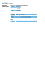
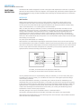
Absolute Maximum ratings
Absolute maximum ratings for supply voltage and voltages on digital and analogue pins of the
Module are listed below. Exceeding these values will cause permanent damage.
Parameter
Min
Peak current of power supply
Max
Unit
550
mA
Voltage at digital pins
-0.3
3.3
V
Voltage at VCC_5V pin
3.3
5
V
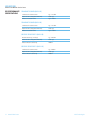
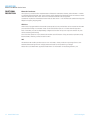
Recommended Operating Parameters
Power Supply
Signal Name
Pin No
Voltage level
Comments
VCC_5V
28, 29, 31
3.3V to 5.0V
Ityp = 250mA.
All VCC_5V pins should be connected
GND
11,15,18,30,36,38
All six GND pins should be connected
Signal Levels for Interface and GPIO
Signal Type
Signal level Signal level @ 0mA load Signal level @ 4mA load
Input
VILmax=0.8V
VIHmin=2.1V
VIHmax=3.3V
Output
VOLmax=0.2V
VOHmin=2.8V
VOLmax=0.4V
VOHmin=2.6V
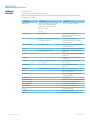
RS-232 Interface
Signal Name
Pin No
I/O
UART_TX
21
O
Comments
UART_RX
25
I
UART_CTS
19
I
UART_RTS
23
O
UART_DSR
10
I
Used to place the module in Powersave 2 mode
UART_DTR
12
O
Direction is programmable – default is Output
UART_RI
6
O
Direction is programmable – default is Output
UART_DCD
8
O
Direction is programmable – default is Output
This pin must NOT be pulled low by external circuitry.
General Purpose I/O and ADC
Signal Name
Pin No
I/O
Comments
GPIO 1 - 9
2,4,14,16,33,35,37,39
I or O
There is no GPIO3
GPIO 10 – 13
10,12,6,8
I or O
Shared with DSR, DTR, RI, DCD
ADC0, ADC1
1, 3
I
Range 0 – 3.0V
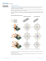
Other Functions
Signal Name
10 www.lairdtech.com
Pin No
I/O
RESET
13
I
Comments
Active high. The RESET line has a fixed 10kOhm pull down
resistor to ground, followed by a 10kOhm resistor feeding
the base of a transistor.
3VOUT
27
O
Used to monitor the state of the regulated supply within
the module. THIS PIN MUST NOT BE USED TO POWER AN
EXTERNAL CIRCUIT.
Laird Technologies