1
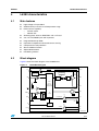
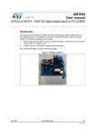
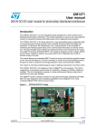
UM1491
User manual
100 W 3-phase inverter demonstration board using the
L6390 and STD5N52U for vector control
Introduction
The 100 W 3-phase inverter demonstration board features the L6390 and STD5N52U for
field-oriented control (FOC) of permanent magnet synchronous motors (PMSM). Also
referred to by order code STEVAL-IHM021V2, this 3-phase inverter is designed to perform
the FOC of sinusoidal-shaped back-EMF PMSMs with or without sensors, with nominal
power up to 100 W. The flexible, open, high-performance design consists of a 3-phase
inverter bridge based on:
■
the STD5N52U power MOSFET in a DPAK package, with enhanced fast body-drain
recovery diode
■
the L6390 device, which is part of the latest high-voltage half-bridge gate driver family
featuring an integrated comparator for implementation of hardware protection (i.e.
overcurrent, overtemperature, etc.)
■
an embedded operational amplifier suitable for advanced current sensing
The system is specifically designed to achieve fast and accurate conditioning of the current
feedback, thereby matching the requirements typical of high-end applications such as fieldoriented motor control. As an alternative to the STD5N52U, the STGD6NC60HD or
STGDL6NC60DI IGBT devices may be used on the board without replacing the switch
driving network.
The board is compatible with 110 and 230 Vac mains, and includes a power supply stage
with the VIPer12A-E (in buck configuration) to generate the +15 V and +3.3 V supply voltage
required by the application. Finally, the board can be interfaced with the STM3210B-EVAL
(STM32 microcontroller demonstration board) through a dedicated connector.
Figure 1.
STEVAL-IHM021V2 demonstration board
!-V
November 2011
Doc ID 022479 Rev 1
1/25
www.st.com
Contents
UM1491
Contents
1
Main features . . . . . . . . . . . . . . . . . . . . . . . . . . . . . . . . . . . . . . . . . . . . . . . 4
1.1
Target applications . . . . . . . . . . . . . . . . . . . . . . . . . . . . . . . . . . . . . . . . . . . 4
2
System architecture . . . . . . . . . . . . . . . . . . . . . . . . . . . . . . . . . . . . . . . . . 5
3
Safety and operating instructions . . . . . . . . . . . . . . . . . . . . . . . . . . . . . . 6
4
3.1
General . . . . . . . . . . . . . . . . . . . . . . . . . . . . . . . . . . . . . . . . . . . . . . . . . . . . 6
3.2
Intended use of the demonstration board . . . . . . . . . . . . . . . . . . . . . . . . . . 6
3.3
Installing the demonstration board . . . . . . . . . . . . . . . . . . . . . . . . . . . . . . . 6
3.4
Electronic connections . . . . . . . . . . . . . . . . . . . . . . . . . . . . . . . . . . . . . . . . 6
3.5
Operating the demonstration board . . . . . . . . . . . . . . . . . . . . . . . . . . . . . . 7
L6390 characteristics . . . . . . . . . . . . . . . . . . . . . . . . . . . . . . . . . . . . . . . . 8
4.1
Main features . . . . . . . . . . . . . . . . . . . . . . . . . . . . . . . . . . . . . . . . . . . . . . . 8
4.2
Block diagram . . . . . . . . . . . . . . . . . . . . . . . . . . . . . . . . . . . . . . . . . . . . . . . 8
5
STD5N52U characteristics . . . . . . . . . . . . . . . . . . . . . . . . . . . . . . . . . . . . 9
6
Electrical characteristics of the board . . . . . . . . . . . . . . . . . . . . . . . . . 10
7
Board architecture . . . . . . . . . . . . . . . . . . . . . . . . . . . . . . . . . . . . . . . . . . 11
8
2/25
7.1
Power supply . . . . . . . . . . . . . . . . . . . . . . . . . . . . . . . . . . . . . . . . . . . . . . 11
7.2
Gate driving . . . . . . . . . . . . . . . . . . . . . . . . . . . . . . . . . . . . . . . . . . . . . . . 12
7.3
Amplifying network . . . . . . . . . . . . . . . . . . . . . . . . . . . . . . . . . . . . . . . . . . 12
7.4
Brake feature . . . . . . . . . . . . . . . . . . . . . . . . . . . . . . . . . . . . . . . . . . . . . . 12
7.5
Temperature feedback . . . . . . . . . . . . . . . . . . . . . . . . . . . . . . . . . . . . . . . 12
STEVAL-IHM021V2 schematic diagrams . . . . . . . . . . . . . . . . . . . . . . . . 13
8.1
Gate driving circuit . . . . . . . . . . . . . . . . . . . . . . . . . . . . . . . . . . . . . . . . . . 15
8.2
Overcurrent protection . . . . . . . . . . . . . . . . . . . . . . . . . . . . . . . . . . . . . . . 15
8.3
Current sensing amplifying network . . . . . . . . . . . . . . . . . . . . . . . . . . . . . 16
8.4
Brake function . . . . . . . . . . . . . . . . . . . . . . . . . . . . . . . . . . . . . . . . . . . . . 17
Doc ID 022479 Rev 1
UM1491
9
Contents
Using the STEVAL-IHM021V2 with the “STM32 PMSM FOC SDK v3.0”
firmware library 19
9.1
Environmental considerations . . . . . . . . . . . . . . . . . . . . . . . . . . . . . . . . . 19
9.2
Hardware requirements . . . . . . . . . . . . . . . . . . . . . . . . . . . . . . . . . . . . . . 20
9.3
Software requirements . . . . . . . . . . . . . . . . . . . . . . . . . . . . . . . . . . . . . . . 20
9.4
Configuration of STM32 PMSM FOC SDK v3.0 for the STEVAL-IHM021v2
21
10
References . . . . . . . . . . . . . . . . . . . . . . . . . . . . . . . . . . . . . . . . . . . . . . . . 23
11
Revision history . . . . . . . . . . . . . . . . . . . . . . . . . . . . . . . . . . . . . . . . . . . 24
Doc ID 022479 Rev 1
3/25
List of figures
UM1491
List of figures
Figure 1.
Figure 2.
Figure 3.
Figure 4.
Figure 5.
Figure 6.
Figure 7.
Figure 8.
Figure 9.
Figure 10.
Figure 11.
Figure 12.
4/25
STEVAL-IHM021V2 demonstration board . . . . . . . . . . . . . . . . . . . . . . . . . . . . . . . . . . . . . . 1
Motor control system architecture. . . . . . . . . . . . . . . . . . . . . . . . . . . . . . . . . . . . . . . . . . . . . 6
L6390 block diagram . . . . . . . . . . . . . . . . . . . . . . . . . . . . . . . . . . . . . . . . . . . . . . . . . . . . . . 9
STD5N52U . . . . . . . . . . . . . . . . . . . . . . . . . . . . . . . . . . . . . . . . . . . . . . . . . . . . . . . . . . . . . 10
STEVAL-IHM021V2 block diagram . . . . . . . . . . . . . . . . . . . . . . . . . . . . . . . . . . . . . . . . . . 12
Power supply block diagram . . . . . . . . . . . . . . . . . . . . . . . . . . . . . . . . . . . . . . . . . . . . . . . . 12
Inverter schematic . . . . . . . . . . . . . . . . . . . . . . . . . . . . . . . . . . . . . . . . . . . . . . . . . . . . . . . 14
Power supply schematics . . . . . . . . . . . . . . . . . . . . . . . . . . . . . . . . . . . . . . . . . . . . . . . . . . 15
Detailed gate driving circuit. . . . . . . . . . . . . . . . . . . . . . . . . . . . . . . . . . . . . . . . . . . . . . . . . 16
Current sensing amplifying network . . . . . . . . . . . . . . . . . . . . . . . . . . . . . . . . . . . . . . . . . . 17
Brake circuit . . . . . . . . . . . . . . . . . . . . . . . . . . . . . . . . . . . . . . . . . . . . . . . . . . . . . . . . . . . . 18
Example of isolation circuit for Triac-based application . . . . . . . . . . . . . . . . . . . . . . . . . . . 20
Doc ID 022479 Rev 1
UM1491
1
Main features
Main features
The STEVAL-IHM021V2 100 W 3-phase inverter has the following characteristics:
1.1
●
Wide range input voltage
●
Maximum power up to 100 W at 230 Vac input
●
The STD5N52U 4.4 A, 520 V power MOSFET
●
Compatibility with other power switches in DPAK packages (the STGD6NC60HD or
STGDL6NC60DI, for example)
●
15 V auxiliary power supply connector
●
Connector for interfacing with the STM3210B-EVAL board
Target applications
●
Refrigerator compressors
●
Dishwasher pumps
Doc ID 022479 Rev 1
5/25
System architecture
2
UM1491
System architecture
A generic motor control system can be schematized as the arrangement of four main blocks
(Figure 2).
●
Control block: its main tasks are to accept user command and motor drive configuration
parameters, and to provide digital signals to implement the appropriate motor driving
strategy
●
Power block: it performs the power conversion from the DC bus, transferring it to the
motor by means of a 3-phase inverter topology
●
The motor: the STEVAL-IHM021V2 board can drive any PMSM, but the FOC itself is
conceived for sinusoidal-shaped back-EMF
●
Power supply block: it can accept input voltages of 86 to 260 Vac and provides the
appropriate levels to supply both the control block and power block devices
Figure 2.
Motor control system architecture
#ONTROL
BLOCK
0OWER
SUPPLY
0OWER
BLOCK
-OTOR
!-V
Of the above motor control system architecture, the STEVAL-IHM021V2 includes the Power
Supply and Power hardware blocks.
The power block, based on the high voltage gate driver L6390 and power MOSFET
STD5N52U, converts the signals coming from the control block into power signals capable
of correctly driving the 3-phase inverter, and therefore the motor.
The power supply can be fed with 110 or 230 Vac mains, and the maximum allowed input
power is 100 W at 230 Vac (refer to Section 7).
In the control block, a J3 connector is mounted on both the STEVAL-IHM021V2 and the
STM3210B-EVAL, which allows the STM32 microcontroller demonstration board to be used
as a hardware platform for development. Minor modifications may be applied to the “STM32
FOC firmware libraries v2.0” for these to be used as a software platform for the sensorless
control of PMSMs (see Section 9.4).
6/25
Doc ID 022479 Rev 1
UM1491
Safety and operating instructions
3
Safety and operating instructions
3.1
General
Warning:
During assembly and operation, the STEVAL-IHM021V2
demonstration board poses several inherent hazards,
including bare wires, moving or rotating parts and hot
surfaces. Serious personal injury and damage to property
may occur if the kit or its components are used or installed
incorrectly.
All operations involving transportation, installation and use, as well as maintenance, should
be performed by skilled technical personnel (applicable national accident prevention rules
must be observed). Skilled technical personnel refers to suitably-qualified people who are
familiar with the installation, use and maintenance of electronic power systems.
3.2
Intended use of the demonstration board
The STEVAL-IHM021V2 demonstration board is designed for demonstration purposes only,
and must not be used for electrical installations or machinery. Technical data and
information concerning the power supply conditions are detailed in the documentation and
should be strictly observed.
3.3
Installing the demonstration board
The installation and cooling of the demonstration board must be in accordance with the
specifications and target application.
3.4
●
The motor drive converters must be protected against excessive strain. In particular,
components should not be bent or isolating distances altered during transportation or
handling.
●
No contact must be made with other electronic components and contacts.
●
The board contains electrostatically-sensitive components that are prone to damage if
used incorrectly. Do not mechanically damage or destroy the electrical components
(potential health risks).
Electronic connections
Applicable national accident prevention rules must be followed when working on the main
power supply with a motor drive. The electrical installation must be completed in accordance
with the appropriate requirements (for example, cross-sectional areas of conductors, fusing,
PE connections, etc.).
Doc ID 022479 Rev 1
7/25
Safety and operating instructions
3.5
UM1491
Operating the demonstration board
A system architecture that supplies power to the STEVAL-IHM021V2 demonstration board
must be equipped with additional control and protective devices in accordance with the
applicable safety requirements (i.e., compliance with technical equipment and accident
prevention rules).
Warning:
8/25
Do not touch the demonstration board after it has been
disconnected from the voltage supply as several parts and
power terminals containing possibly-energized capacitors
need time to discharge.
Doc ID 022479 Rev 1
UM1491
L6390 characteristics
4
L6390 characteristics
4.1
Main features
4.2
●
High voltage rail up to 600 V
●
dV/dt immunity ± 50 V/ns in full temperature range
●
Driver current capability:
–
270 mA source
–
430 mA sink
●
Switching times 75/35 ns RISE/FALL with 1 nF load
●
3.3, 5 V TTL/CMOS inputs with hysteresis
●
Integrated bootstrap diode
●
Operational amplifier for advanced current sensing
●
Comparator for fault protection
●
Smart shutdown function
●
Adjustable dead time
●
Interlocking function
Block diagram
Figure 3 shows the block diagram of the L6390 device.
Figure 3.
L6390 block diagram
"//4342!0$2)6%2
6##
&,/!4).'3425#452%
FROM,6'
56
$%4%#4)/.
56
$%4%#4)/.
(6'
$2)6%2
3
,%6%,
3()&4%2
().
2
(6'
,/')#
6
3(//4
4(2/5'(
02%6%.4)/.
,).
"//4
/54
6##
,6'
$2)6%2
,6'
3$/$ '.$
3$
,!4#(
3-!24
3$
6
#/-0!2!4/2
#0
62%&
$4
/0/54
$%!$
6##
4)-%
/0!-0
/0
/0
!-V
Doc ID 022479 Rev 1
9/25
STD5N52U characteristics
5
UM1491
STD5N52U characteristics
The STD5N52U is an N-channel power MOSFET in a DPAK package (520 V, 1.22 Ω,
4.4 A). The Zener-protected STD5N52U employs UltraFASTmesh™ technology and has
been specifically designed for applications where a body-drain diode with an extremely low
trr is required (motor control, lighting in full bridge topology, inverters for LCD TV, etc.).
Figure 4.
STD5N52U
)
,
$0!+
8
!-V
●
VDSS = 520 V
●
RDS(on) < 1.5 Ω
●
ID = 4.4 A
Table 1.
STD5N52U absolute maximum ratings
Symbol
Parameter
Value
Unit
VDS
Drain-source (VGS = 0)
520
V
VDGR
Drain-gate voltage (RGS = 20 kΩ)
520
V
VGS
Gate-source voltage
±30
V
ID
Drain current (continuous) at TC = 25°C
4.4
A
ID
Drain current (continuous) at TC = 100°C
2.7
A
IDM(1)
Drain current (pulsed)
17.6
A
PTOT
Total dissipation at TC = 25°C
70
W
1. Pulse width limited by safe operating area.
Note:
10/25
Stresses above the limits shown in Table 1 may cause permanent damage to the device.
Doc ID 022479 Rev 1
UM1491
6
Electrical characteristics of the board
Electrical characteristics of the board
Stresses above the limits shown in Table 2 may cause permanent damage to the devices
present inside the board. These are stress ratings only and functional operation of the
device under these conditions is not implied. Exposure to maximum rating conditions for
extended periods may affect device reliability.
A 15 V bias current measurement may be useful to check the working status of the board. If
the measured value is considerably higher than the typical value, some damage has
occurred to the board. Supply the control board using a 15 V power supply connected to
J10, respecting the polarity.
Table 2.
Board electrical characteristics
STEVAL-IHM021V2
Unit
Board parameters
Min
Max
15 V auxiliary supply range - J10
14.5
17
V
15 V bias current (typical)
8
10
mA
Vmains - J7
30
270
Vac
Warning:
To avoid damaging the board when feeding the +15 V voltage
supply through the auxiliary connector (J10), remove jumper
J8 and supply the +15 V before connecting the mains.
Doc ID 022479 Rev 1
11/25
Board architecture
7
UM1491
Board architecture
The STEVAL-IHM021V2 can be schematized as shown in Figure 5.
Figure 5.
STEVAL-IHM021V2 block diagram
/
9
/
3RZHU
6XSSO\
/
9EXV
+
.
.
.
0
56KXQW
56KXQW
56KXQW
17&
,$
+,1 /,1
,% +,1 /,1
)$8/7
,& +,1 /,1
RSWLRQDO
-&RQQHFWRU
%5$.(
!-V
7.1
Power supply
The power supply can address an AC input voltage ranging from 30 Vac up to 270 Vac. The
alternating current input is rectified by a diode bridge and a bulk capacitor to generate a
direct current bus voltage approximately equal to √2 Vac (neglecting the voltage drop across
the diodes and the bus voltage ripple). A VIPer12A-E is then used in a buck converter
configuration to generate the +15-V supply voltage of the gate drivers. Finally, a linear
regulator (L78L33ABUTR) is used to generate the 3.3 V used to pull up the low-side gate
driver inputs so as to prevent the undesired turn-on of low-side switches when the J5
connector is unplugged.
Figure 6 shows a block diagram of the power supply.
Figure 6.
Power supply block diagram
!-V
12/25
Doc ID 022479 Rev 1
UM1491
7.2
Board architecture
Gate driving
As mentioned previously, gate driving of the switches is performed by the latest of the L6390
family of devices. Refer to Section 8.1 for detailed information on the gate driving circuit and
dead-time insertion. A fault signal is also fed back to the J5 connector if an overcurrent event
is detected.
7.3
Amplifying network
The voltages across the three shunt resistors are amplified by K to correctly condition the
current feedback signals and optimize the output voltage range for a given phase current
range and A/D converter input dynamics. Refer to Section 8.3 for more detailed information
on how to dimension the op-amp conditioning network depending on your needs.
7.4
Brake feature
The brake feature performs motor braking by switching simultaneously to the low-side power
MOSFET, thus shortening the motor phases.
Warning:
7.5
This feature is mandatory in applications that require the
motor to operate in a flux-weakening region. In these
conditions, the back-EMF generated by the rotor’s spinning is
greater than the bus voltage, and the brake feature prevents
the motor from acting as a generator and destructively
charging the bus capacitance. Refer to Section 8.4 for
additional information.
Temperature feedback
Temperature feedback is performed by way of an NTC. It enables monitoring of the power
stage temperature so as to prevent any damage to the inverter caused by overtemperature.
Doc ID 022479 Rev 1
13/25
Doc ID 022479 Rev 1
10
N
5
23287
23287B5&
10
&
N
5
23287
%$5&),/0
23287B5&
10
&
N
5
23287
%$5&),/0
9
5
N
-
N
5
N
N
&
Q)
&
S)
5
23287
/62
5
23287
/,1 9%227
6'2' +9*
+,1
287
1&
9&&
'7
1&
/9*
23
23287 &3
23
*1'
56PRGHO&
17&N
17&
7HPS
Q)
&
&
S)
N
5
/62
&
S)
N
5
5
9
&
S)
N
5
9
5
5
10
5
5
10
9
Q)
5
10
9
&
5
Q)
&
5
5
10
9
5
10
5
10
5
Q)
&
5
N
5 5 5 5 Q)
N
5 5 &
N
5 5 Q)
&
5
5 5 '
160'
'
160'
'
160'
'
160'
'
160'
+9
+9
5 5
5
5
4
67'18
287
4
67'18
5
5
5 5
4
67'18
287
4
67'18
5 5
5 5
4
67'18
287
4
67'18
&
Q)
&
N
5
N
5
-
/,1 9%227
6'2' +9*
287
+,1
1&
9&&
'7
1&
/9*
23
23287 &3
23
*1'
5
Q)
&
9
5 9
N
5
9FF
Q)
&
23287
&
S)
N
5
9
Q)
+9
'
%$5&),/0
Q)
&
S)
&
&
S)
N
N
5
N
5
/62
5
'
160'
9
S)
&
'
N
5
9FF
Q)
&
-
/,1 9%227
6'2' +9*
+,1
287
9&&
1&
'7
1&
23
/9*
23287 &3
23
*1'
Inverter schematic
%$5&),/0
9
&
S)
S)
&
%$5&),/0
'
Q)
&
5
Figure 7.
23287B5&
'
5
N
S)
&
N
5
S)
&
STEVAL-IHM021V2 schematic diagrams
9
N
5
5
N
Q)
&
9
5
N
5
N
5
N
S)
&
9FF
&
8
'
9GG
+,1
/,1
-3 23(1
N
5
9
N
5
&
S)
%$5&),/0
23287B5&
23287B5&
23287B5&
S)
+,1
/,1
-3 23(1
9
5
N
'
+9%XV
7HPS
N
5
&
9SXOO
Q)
&
9
N
5
5
N
+,1
/,1
N
5
N
-3 23(1
+,1
/,1
+,1
/,1
4
%&
+,1
/,1
9
5
6'
7HPS
+9%XV
N
5
(QF=
9SXOO
(QF$
(QF%
(QF=
&
S)
(QF%
-
&21$
&
S)
(QF$
'
%$5&),/0
6'
&
S)
N
N
N
-
02725B&211
5
5
5
Q)
&
9GG 9
(QF$
(QF%
(QF=
5
10
X)
&
9
6'
6WULSOLQHP[
5
10
*1'
//$%875
9RXW +,1
/,1
+,1
/,1
+,1
/,1
23287B5&
23287B5&
23287B5&
$+
%+
=+
-
9LQ
8
5
10
9SXOO
Q)
&
14/25
9FF
STEVAL-IHM021V2 schematic diagrams
UM1491
!-V
#/.
*
-/4/2
-!).3
*
&53%
/54
/54
/54
#
N&
$
344(,!
$
344(,!
$
3-"94
2
/HM
$
3-"94
.4#
&
#
N&
U&
6
#
$
"!4 7&),-
":8#
23#ODE
:
$
3-"94
$
3-"94
#/.
&"
6$$
6
2%3
3%4
3/52#%
$2!).
Doc ID 022479 Rev 1
#
N&
(6
2
K
,
5
6)0%2!3
$
3-!*!42
#
U&
6
6CC
3TRIPLINEMX
*UMPERTOBEREMOVEDIF6EXTSUPPLYISUSED
*
(6
#
U&6
M(!
23#ODE
*
6EXTSUPPLY
#/.
6
'.$
2
K
7
2
K
7
6
(6"US
$
"!2&),-
Figure 8.
UM1491
STEVAL-IHM021V2 schematic diagrams
Power supply schematics
!-V
15/25
STEVAL-IHM021V2 schematic diagrams
8.1
UM1491
Gate driving circuit
Figure 9 shows the circuit used to turn the power MOSFETs on and off.
Detailed gate driving circuit
5
' 160'
5 Figure 9.
4
67'18
!-V
During the turn-on phase, the power MOSFET gate capacitances are charged through 50-Ω
resistors while the turn-off is secured by the D3 diode (or similar).
Use of the L6390 device guarantees a minimum adjustable dead time (DT). This dead time
is applied to the HVG and LVG outputs whenever a dead time shorter than DT is present on
the HIN and LIN inputs. The R12, R32 and R52 values being equal to 47 kΩ, set the
minimum dead time to approximately 600 ns.
8.2
Overcurrent protection
Hardware overcurrent protection has been implemented on the board, taking advantage of
the comparator integrated inside the L6390. The internal connection between the
comparator output and the shutdown block makes the intervention time of the overcurrent
protection extremely low, slightly above 100 ns.
Since the overcurrent protection acts as soon as the voltage on CP+ rises above Vref
(approximately equal to 0.53 V), and given the default value of the shunt resistors (equal to
1.8/4 =0.45 Ω), it follows that the default value for the maximum allowed current (ICP) is
equal to:
Equation 1
ICP =
VRef
≅ 1.15 A
R shunt
If necessary, the threshold can be decreased by adding R37 (and similarly R55 and R18)
with the formula:
Equation 2
ICP =
1
R shunt
⋅
R40 + R37 ⎡
R40
⎤
Vref − 3.3
⎢
R37
R37 + R40 ⎥⎦
⎣
with R37 >> R40
Similarly, the threshold can be increased by adding R44 (and similar) with the formula:
Equation 3
ICP =
16/25
Vref ⎛ R40 ⎞
⋅ ⎜1 +
⎟
R shunt ⎝ R44 ⎠
Doc ID 022479 Rev 1
with R37 >> R40
UM1491
Current sensing amplifying network
Figure 10 shows the current sensing amplifying network during phase 2.
'7
23
23287
*1'
1&
/9*
&3
23
Figure 10. Current sensing amplifying network
9
5
5
N
N
4
67'18
/62
5
N
5
5
23287
5
5 5
5
&
S)
&
S)
5
N
8.3
STEVAL-IHM021V2 schematic diagrams
!-V
The voltage at node “OPOUT2” can be computed as the sum of a bias and a signal
component, respectively equal to:
Equation 4
VBIAS = 3.3
R41//R43
⎛ R38 + R39 ⎞
⎜1 +
⎟
R36 + R41//R43 ⎝
R42
⎠
Equation 5
VSIGN = I ⋅ R SHUNT ⋅
R36//R43
⎛ R38 + R39 ⎞
⎜1 +
⎟
R41 + R36//R43 ⎝
R42
⎠
With the default values this gives:
●
VBIAS = 1.86 V
●
VSIGN = 2.91⋅ RSHUNT ⋅ I
As such, the maximum current amplifiable without distortion is equal to:
Equation 6
IMAX =
3.3 − 1.86
0.495
=
= 1 .1 A
2.91⋅ R SHUNT RSHUNT
Doc ID 022479 Rev 1
17/25
STEVAL-IHM021V2 schematic diagrams
UM1491
Note that the IMAX value can be modified by simply changing the values of the shunt
resistors.
8.4
Brake function
The STEVAL-IHM021V2 demonstration board provides a brake function that, through the
pull-up of a single brake signal, simultaneously turns the three low-side switches ON,
shorting the 3-phase load. The feature is accessed using one single small-signal bipolar
transistor (Q7), whose function is to pull down the cathodes of six small signal diodes
connected to each of the six logic inputs (HIN1, LIN 1, HIN2, LIN 2 , HIN3, LIN 3 ) of the
L6390 gate drivers. The in-series resistors together with the input lines avoid any conflict
with the external controller input signals, giving priority to the brake signal (see Figure 11).
Figure 11. Brake circuit
!-V
The brake signal is active high and 3.3/5 V compatible.
Table 3.
Truth table
HINx
LIN x
x
x
x
SD
Brake
LVGx
HVGx
Load
0
x
0
0
Tri-state
x
1
1
1
0
brake
0
0
1
0
1
0
0
1
1
0
0
0
1
0
1
0
0
0
1
1
1
0
0
1
Normal operation
Warning:
18/25
This feature is mandatory in applications that require the
motor to operate in the flux-weakening region. In these
conditions, the back-EMF generated by the rotor spinning is
greater than the bus voltage and the brake feature prevents
the motor from acting as a generator, and destructively
charging the bus capacitance.
Doc ID 022479 Rev 1
UM1491
Using the STEVAL-IHM021V2 with the “STM32 PMSM FOC SDK v3.0” firmware library
9
Using the STEVAL-IHM021V2 with the “STM32 PMSM
FOC SDK v3.0” firmware library
The “STM32 PMSM FOC SDK v3.0” is a firmware library for STM32 that can be used in
conjunction with STEVAL-IHM021v2 to perform the field-oriented control (FOC) of a
permanent magnet synchronous motor (PMSM) in both sensor and sensorless
configurations.
This section describes how to configure “STM32 PMSM FOC SDK v3.0” with its related PC
configuration tool (ST MC Workbench) in order to be compatible with the STEVALIHM021V2.
9.1
Environmental considerations
Warning:
The STEVAL-IHM021V2 demonstration board must only be
used in a power laboratory. The voltage used in the drive
system presents a shock hazard.
The kit is not electrically isolated from the DC input. This topology is very common in motor
drives. The microprocessor is grounded by the integrated ground of the DC bus. The
microprocessor and associated circuitry are hot and MUST be isolated from user controls
and communication interfaces.
Warning:
Any measurement equipment must be isolated from the main
power supply before powering up the motor drive. To use an
oscilloscope with the kit, it is safer to isolate the DC supply
AND the oscilloscope. This prevents a shock from occurring
as a result of touching any single point in the circuit, but
does NOT prevent shocks when touching two or more points
in the circuit.
An isolated AC power supply can be constructed using an isolation transformer and a
variable transformer. An example of an isolation circuit in a Triac-based application is shown
in figure 13. Although this application note was written for Triac, the isolation constraints still
apply for switching semiconductor devices such as MOSFETs.
Note:
Isolating the application rather than the oscilloscope is highly recommended in any case.
Doc ID 022479 Rev 1
19/25
Using the STEVAL-IHM021V2 with the “STM32 PMSM FOC SDK v3.0” firmware library
UM1491
Figure 12. Example of isolation circuit for Triac-based application
02/"%
,).%
23
#/-054%2
%-5,!4/2
6
,).%
6
6
,/!$
0/7%2
3500,9
/3#),,/3#/0%
,).%
).35,!4%$3934%-
!-V
9.2
Hardware requirements
The following items are required to run a permanent magnet synchronous motor with the
STEVAL-IHM021V2 and “STM32 PMSM FOC SDK v3.0”:
●
The STEVAL-IHM021V2 board
●
Any available STM32-based control stage featuring a motor control connector (e.g.
STM32100B-EVAL)
●
A high-voltage insulated AC power supply up to 230 Vac
●
A J-link programmer (not included in the package)
●
A J-link insulating board (not included in the package)
●
A 3-phase brushless motor with permanent magnet rotor (not included in the package)
●
An insulated oscilloscope (as necessary)
●
An insulated multimeter (as necessary)
9.3
Software requirements
To customize, compile and download the “STM32 PMSM FOC SDK v3.0” motor control
firmware, the IAR tool “EWARM v6.10” (or later) must be installed. The free, 32 k limited
version (referenced as the “KickStart” version) is available for downloading at:
http://supp.iar.com/Download/SW/?item=EWARM-KS32-442A.
Web distribution of “STM32 PMSM FOC SDK v3.0” can be downloaded from:
http://www.st.com/internet/com/SOFTWARE_RESOURCES/SW_COMPONENT/FIRM
WARE/stm32_pmsm_foc_motorcontrol_fwlib.zip
The ST MC Workbench PC configuration tool for “STM32 PMSM FOC SDK v3.0” can be
downloaded from:
http://www.st.com/internet/com/SOFTWARE_RESOURCES/TOOL/CONFIGURATION
_UTILITY/motorcontrol_workbench.zip
20/25
Doc ID 022479 Rev 1
UM1491
Using the STEVAL-IHM021V2 with the “STM32 PMSM FOC SDK v3.0” firmware library
Refer to user manual UM1052 “STM32F103xx or STM32F100xx PMSM single/dual FOC
SDK v3.0” for detailed information about “STM32 PMSM FOC SDK v3.0”
9.4
Configuration of STM32 PMSM FOC SDK v3.0 for the
STEVAL-IHM021v2
When using the ST MC Workbench configuration PC tool, the following parameters should
be set in the “Power stage” section:
Table 4.
ST MC Workbench configuration PC tool: power stage parameters
Parameter
STEVAL-IHM032v1
default value
Unit
ICL Shutout
Disabled
Dissipative brake
Disabled
Bus voltage sensing
Enabled
Bus voltage divider
125
Min rated voltage
60
V
Max rated voltage
380
V
Nominal voltage
325
V
Temperature sensing
Enabled
(1)
1055
mV
25
°C
∆V/∆T
22
mV/°C
Max working temperature on sensor
70
°C
Overcurrent protection
Enabled
Comparator threshold
0.5
V
Overcurrent network gain
0.45
V/A
Expected overcurrent threshold
1.11
A
Overcurrent feedback signal polarity
Active low
Overcurrent protection disabling network
Enabled
Overcurrent protection disabling network polarity
Active high
Current sensing
Enabled
Current reading topology
Three shunt resistor
Shunt resistor(s) value
0.45
Amplifying network gain
2.9
T-noise
1250
ns
T-rise
1250
ns
Power switches: min dead-time
500
ns
Power switches: max switching frequency
50
kHz
V0
T0
(1)
Doc ID 022479 Rev 1
Ω
21/25
Using the STEVAL-IHM021V2 with the “STM32 PMSM FOC SDK v3.0” firmware library
Table 4.
ST MC Workbench configuration PC tool: power stage parameters
Parameter
STEVAL-IHM032v1
default value
U,V,W driver: high side driving signal
Active high
U,V,W driver: low side driving signal complemented from high side
Disabled
U,V,W driver: low side driving signal polarity
Active low
1. These values are computed for Vdd_micro = 3.3 V
22/25
UM1491
Doc ID 022479 Rev 1
Unit
UM1491
10
References
References
This user manual provides information on the hardware features and use of the STEVALIHM021V2 demonstration board. For additional information on supporting software and
tools, refer to the following:
●
STD5N52U datasheet
●
L6390 datasheet
●
http://www.st.com/mcu/ web site, which is dedicated to the complete
STMicroelectronics microcontroller portfolio.
Doc ID 022479 Rev 1
23/25
Revision history
11
UM1491
Revision history
Table 5.
24/25
Document revision history
Date
Revision
10-Nov-2011
1
Changes
Initial release.
Doc ID 022479 Rev 1
UM1491
Please Read Carefully:
Information in this document is provided solely in connection with ST products. STMicroelectronics NV and its subsidiaries (“ST”) reserve the
right to make changes, corrections, modifications or improvements, to this document, and the products and services described herein at any
time, without notice.
All ST products are sold pursuant to ST’s terms and conditions of sale.
Purchasers are solely responsible for the choice, selection and use of the ST products and services described herein, and ST assumes no
liability whatsoever relating to the choice, selection or use of the ST products and services described herein.
No license, express or implied, by estoppel or otherwise, to any intellectual property rights is granted under this document. If any part of this
document refers to any third party products or services it shall not be deemed a license grant by ST for the use of such third party products
or services, or any intellectual property contained therein or considered as a warranty covering the use in any manner whatsoever of such
third party products or services or any intellectual property contained therein.
UNLESS OTHERWISE SET FORTH IN ST’S TERMS AND CONDITIONS OF SALE ST DISCLAIMS ANY EXPRESS OR IMPLIED
WARRANTY WITH RESPECT TO THE USE AND/OR SALE OF ST PRODUCTS INCLUDING WITHOUT LIMITATION IMPLIED
WARRANTIES OF MERCHANTABILITY, FITNESS FOR A PARTICULAR PURPOSE (AND THEIR EQUIVALENTS UNDER THE LAWS
OF ANY JURISDICTION), OR INFRINGEMENT OF ANY PATENT, COPYRIGHT OR OTHER INTELLECTUAL PROPERTY RIGHT.
UNLESS EXPRESSLY APPROVED IN WRITING BY TWO AUTHORIZED ST REPRESENTATIVES, ST PRODUCTS ARE NOT
RECOMMENDED, AUTHORIZED OR WARRANTED FOR USE IN MILITARY, AIR CRAFT, SPACE, LIFE SAVING, OR LIFE SUSTAINING
APPLICATIONS, NOR IN PRODUCTS OR SYSTEMS WHERE FAILURE OR MALFUNCTION MAY RESULT IN PERSONAL INJURY,
DEATH, OR SEVERE PROPERTY OR ENVIRONMENTAL DAMAGE. ST PRODUCTS WHICH ARE NOT SPECIFIED AS "AUTOMOTIVE
GRADE" MAY ONLY BE USED IN AUTOMOTIVE APPLICATIONS AT USER’S OWN RISK.
Resale of ST products with provisions different from the statements and/or technical features set forth in this document shall immediately void
any warranty granted by ST for the ST product or service described herein and shall not create or extend in any manner whatsoever, any
liability of ST.
ST and the ST logo are trademarks or registered trademarks of ST in various countries.
Information in this document supersedes and replaces all information previously supplied.
The ST logo is a registered trademark of STMicroelectronics. All other names are the property of their respective owners.
© 2011 STMicroelectronics - All rights reserved
STMicroelectronics group of companies
Australia - Belgium - Brazil - Canada - China - Czech Republic - Finland - France - Germany - Hong Kong - India - Israel - Italy - Japan Malaysia - Malta - Morocco - Philippines - Singapore - Spain - Sweden - Switzerland - United Kingdom - United States of America
www.st.com
Doc ID 022479 Rev 1
25/25