1
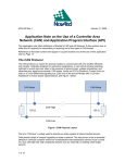
USB3FPGA
V 1.41 February, 26 2008
User Manual C 1030-2805
SPARTAN-3E FPGA board with USB 2.0 interface
Order number: C 1030-2805
USB3FPGA C 1030-2805
User Manual V 1.41
www.cesys.com
preliminary
Copyright information
Copyright © 2007 CESYS GmbH. All Rights Reserved. The information in this
document is proprietary to CESYS GmbH. No part of this document may be
reproduced in any form or by any means or used to make derivative work (such as
translation, transformation or adaptation) without written permission from CESYS
GmbH.
CESYS GmbH provides this documentation without warranty, term or condition of
any kind, either express or implied, including, but not limited to, express and implied
warranties of merchantability, fitness for a particular purpose, and non-infringement.
While the information contained herein is believed to be accurate, such information
is preliminary, and no representations or warranties of accuracy or completeness
are made. In no event will CESYS GmbH be liable for damages arising directly or
indirectly from any use of or reliance upon the information contained in this
document. CESYS GmbH will make improvements or changes in the product(s)
and/or program(s) described in this documentation at any time.
CESYS GmbH retains the right to make changes to this product at any time, without
notice. Products may have minor variations to this publication, known as errata.
CESYS GmbH assumes no liability whatsoever, including infringement of any patent
or copyright, for sale and use of CESYS GmbH products.
CESYS GmbH and the CESYS logo are registered trademarks.
All product names are trademarks, registered trademarks, or service marks of their
respective owner.
⇒ Please check www.cesys.com to get the latest version of this document.
CESYS Gesellschaft für angewandte Mikroelektronik mbH
Zeppelinstrasse 6a
D – 91074 Herzogenaurach
Germany
USB3FPGA C 1030-2805
User Manual V 1.41
www.cesys.com
preliminary
A
Overview
Summary of USB3FPGA
USB3FPGA can be used as a development platform for designs with Xilinx
SPARTAN 3E FPGAs as well as a OEM-component for job lot production.
A 96-pin VG connector allows the attachment of external hardware to the FPGA.
The board is equipped with a XC3S500E-4PQ208C XILINX FPGA, a member of the
Spartan 3E family. This programmable logic device receives its internal functions
after it has been configured by downloading a bitstream that represents the design.
The change of logic functions (reconfiguration) is possible at any time.
The bistream is loaded from the PC via USB to the FPGA. The software that comes
with the board permits to load new configurations anytime.
Two clock oscillators supply basic clocks that can be used by the FPGA. A third
clock oszillator can be populated on request.
The 96-pin VG expansion connector of the USB3FPGA allows connections to I/O
pins of the FPGA as well as to 3.3 V and GND. Many extensions can be attached
directly without the need of an additional external power supply
Feature list
•
•
•
•
•
•
•
•
•
•
•
•
XILINX XC3S500E-4PQ208C FPGA
CYPRESS FX2LP USB controller
2MByte FAST SRAM (1M x 16, 10ns) connected to FPGA
64 kByte SRAM connected to USB 2.0 controller (optional)
USB 2.0 compliant device
Selectable self-powered or bus-powered
Up to three individual onboard clock oscillators
Expansion port (44 IO pins + 15 INPUT pins + 22 auxiliary IO pins)
3 LEDS
All FPGA Pins routed to test connectors
Driver for Windows XPTM, Firmware and Benchmark-program included
Sample code (C++ Source) of test-program included
Minimum requirements
☑ PC with USB 2.0 interface running Windows XPTM
☑ 10 MByte free harddisk space
☑ USB3FPGA board with USB2.0 compliant cable
☑ CESYS USB 2.0 drivers
USB3FPGA C 1030-2805
User Manual V 1.41
-A 1-
www.cesys.com
preliminary
FPGA Design Tools
To simulate and synthesize FPGA designs appropriate tools are needed. Xilinx
offers a toolset called “ISE WebPack” free of charge on their website:
http://www.xilinx.com. The ISE WebPack fully supports the XC3S500E Spartan3EFPGA. There are also other commercial tools available from Xilinx and various other
vendors.
Windows XP Quick-start installation guide
1. Connect USB3FPGA to one free USB2.0 port with shipped USB2.0 compliant
cable.
2. Install USB3FPGA driver via Windows XPTM installation guide from included driver
and utilities CD.
3. With Windows XPTM USB3FPGA device driver has to be installed twice.
4. Locate folder “bin” on shipped CD and double-click “diag.exe”. By pressing the
'Memory Test' button on the left a first device test can be started.
USB3FPGA C 1030-2805
User Manual V 1.41
-A2-
www.cesys.com
preliminary
B
Hardware
USB 2.0
conncetor
High-Speed
USB 2.0
Peripheral
controller
SPARTAN-3E
FPGA
96-pin
VG - connector
2 Mbyte Fast SRAM
1M x 16, 10ns
Clock, Reset
and Power
Figure 1: USB3FPGA block diagram
SPARTAN-3E FPGA
Device
System Gates
CLB Rows
CLB Columns
Total CLBs
Total Slices
Distributed RAM bits
Block RAM bits
Dedicated Multipliers
DCMs
XC3S500E-4PQ208C
500k
46
34
1164
4.656
73 k
360 k
20
4
For details on SPARTAN-3ETM FPGA, please refer to data sheet at:
http://www.xilinx.com/support/documentation/data_sheets/ds312.pdf
USB3FPGA C 1030-2805
User Manual V 1.41
-B 1-
www.cesys.com
preliminary
P 99
P 97
P 94
P 91
P 89
P 86
P 83
P 81
P 78
P 77
P 75
P 72
P 69
P 65
P 63
P 61
P 58
P 56
P 98
P 96
P 93
P 90
P 87
P 84
P 82
P 80
P 76
P 74
P 71
P 68
P 64
P 62
P 60
P 57
P 55
1
P 50
P 49
P 1 09
P 108
P 48
P 1 12
P 11 0
P 45
P 1 15
P 113
P 42
P 1 18
P 116
P 40
P 1 20
P 11 9
P 36
P 1 23
P 12 2
P 33
P 1 26
P 124
P 34
P 32
P 1 28
P 12 7
P 30
P 29
P 1 29
P 130
P 28
P 26
P 1 33
P 132
P 24
P 25
P 1 34
P 135
P 22
P 23
P 1 36
P 137
P 19
P 20
P 1 38
P 139
P 16
P 18
P 1 40
P 142
P 14
P 15
P 1 44
P 145
P 11
P 12
P 1 46
P 147
P8
P9
P 1 48
P 150
P5
P6
P 1 51
P 15 2
P3
P4
P 1 53
P1
P2
P 1 84
P 1 87
P 1 90
P 1 93
P 1 96
P 1 99
P 2 02
P 2 04
P 2 06
P 18 5
P 18 6
P 18 9
P 19 2
P 19 4
P 19 7
P 20 0
P 20 3
P 20 5
P 1 74
P 17 5
P 17 8
P 1 81
P 1 71
P 1 72
P 18 3
P 1 68
P 16 9
P 1 79
P 1 65
P 16 7
P 1 80
P 1 63
P 16 4
P 1 77
P 1 61
1
SRAM
A B C 1
JTAG
P 39
P 35
USB2.0
Controller
USB2.0
P 31
1
CONFIG
LED
1
LEDA PWR
PWR2
P 43
P 41
J4
SPARTAN-3E
FPGA
P 16 2
P 15 9
P 51
P 106
P 16 0
CON1
P 54
P 1 07
P154
P 1 04
J1
P 10 1
P 1 00
RESERVED
P 1 02
32
P 10 3
Connector diagram
Figure 2: USB3FPGA connector diagram
Attention: The Testpin numbering printed on the PCB v1.0 is not correct in the area
marked above. This error has been fixed in PCB v1.1. This document is correct.
USB3FPGA C 1030-2805
User Manual V 1.41
-B2-
www.cesys.com
preliminary
Board dimensions
Figure 3: USB3FPGA board dimensions
Power supply
The USB3FPGA can be configured to be self powered or bus powered. The default
setting is “bus powered”. This means power is provided by the USB bus. If the
USB3FPGA is the only device on the USB bus, most computers should allow a
maximum current of about 500 mA. This may not be true for notebooks.
J1 Power source select
Pin 1 – 2
Self powered (External +5 Volt power supply must be attached to
connector CON1)
Pin 2 – 3
Bus powered (USB power supply)
USB3FPGA C 1030-2805
User Manual V 1.41
-B3-
www.cesys.com
preliminary
The option “self powered” requires an external power supply connected to CON1.
Use this method if your design draws more current than your USB bus can deliver.
Attention: Be careful when using the external power connector. If you apply more
than 5,5 Volts or if you reverse the polarity, the board will permanently fail and may
not be reparable.
Directly after the USB3FPGA board is connected to the USB bus, it must not
consume more then 100mA. This is the current limit (defined by the USB standard)
until the software has called “SetConfiguration”. Most PC’s ignore this restriction but
some USB-hubs measure the current-flow and will report a shortcut condition when
a USB device draws more than 100 mA immediately after it has been plugged.
The option “software controlled” keeps the FPGA, the SRAM and the Pins on CON1
(A3, B3, C3) powered off until “SetConfiguration” was called. As long as the FPGA is
not powered, its I/O pins must be held low (+/- 0.3 Volt).
Attention: When you use “software controlled” power-on behaviour, make sure no
FPGA I/O pin is driven as long as the FPGA is not powered.
J4 Optional power sequencing
Pin 1 – 2
All power supplies will ramp up as soon as +5 Volt are attached.
Pin 2 – 3
Software controlled power on. At startup only FX2LP power supply
will ramp up. Only after the attached USB host grants more than
100mA FX2LP will enable power up of other onboard power supplies.
USB 2.0 interface
The USB 2.0 interface of the board is implemented using an USB I/O controller
outside the FPGA. Therefore FPGA designs do not need to include USB specific
code. Developers do not need to know details about the USB bus. To enable
communication between the FPGA and a program running on the PC, a easy-to-use
API and VHDL sample code come with the board.
v If your design works “stand-alone” and does not require any communication with
the PC, you may ignore the USB interface details and use it only for downloading
your design.
USB3FPGA C 1030-2805
User Manual V 1.41
-B4-
www.cesys.com
preliminary
FPGA pin connections
All FPGA VCCO-Pins on the USB3FPGA board are connected to 3,3 Volt.
The I/O pins of the SPARTAN-3E FPGA do NOT accept 5 Volt Input signals.
When 5 Volt signals are connected without proper level-shifters or series resistors,
the FPGA will immediately become damaged. When 3,3 Volt signals are used with
long traces or cables in conjunction with improper termination, the resulting
overshoot and undershoot can damage the FPGA as well. Please read Xilinx
application note http://direct.xilinx.com/bvdocs/appnotes/xapp659.pdf for details.
! Don’t apply any voltage outside the interval [-0.5V….+3.8V], not even for a few
Nanoseconds. Take care of overshoot / undershoot conditions.
LEDs
LEDs
USER- LED
FPGA I/O pin 140
Power- LED
FPGA is powered ON
Config- LED
FPGA is configured
PWR2- LED
USB controller is powered ON
Power-LED lights up when the FPGA gets power.
PWR2-LED lights up when the board gets power from the USB-bus
Config-LED lights up when the FPGA is configured successfully.
User-LED light up when there is a low level at the corresponding FPGA Pin. The
meaning of this LEDs is defined by the user’s FPGA design.
FPGA Testpins
All FPGA pins are routed to testpoints to ease the connection of measurement
equipment like Logic Analyzers. The relationship between FPGA pins and Testpoints
is printed on the USB3FPGA board and shown in the Connector-Diagram above.
Expansion port CON1
The 96-pin “VG96 abc reverse” external expansion connector (DIN 41612) is of type
“female”. Please use the connector diagram to indicate pin 1. On some connectors,
the numbers are printed upside down.
Mating connectors among others are: RS Components 476-025 or Farnell 104-986
or HARTING order number 0903 196 7921.
Most pins of the FPGA can be configured as input (IN), output (OUT), or bidirectional (I/O). Make sure your FPGA design does not drive pins that are already
driven by external connected logic. This is also important for bi-directional signals.
USB3FPGA C 1030-2805
User Manual V 1.41
-B5-
www.cesys.com
preliminary
CON1
96-pin VG Expansion connector
Pin
A
B
C
1
V5EXT
V5EXT
V5EXT
2
GND
GND
GND
3
V3
V3
V3
4
* FPGA I/O Pin 199
* FPGA I/O Pin 197
* FPGA I/O Pin 196
5
▼ FPGA IN Pin 194
* FPGA I/O Pin 193
* FPGA I/O Pin 192
6
* FPGA I/O Pin 190
* FPGA I/O Pin 189
* FPGA I/O Pin 187
7
▼ FPGA IN Pin 175
▼ FPGA IN Pin 174
* FPGA I/O Pin 172
8
▼ FPGA IN Pin 169
* FPGA I/O Pin 168
* FPGA I/O Pin 167
9
* FPGA I/O Pin 161
* FPGA I/O Pin 160
▼ FPGA IN Pin 159
10
▼ FPGA IN Pin 6
▼ FPGA IN Pin 204
▼ FPGA IN Pin 154
11
* FPGA I/O Pin 153
* FPGA I/O Pin 152
* FPGA I/O Pin 151
12
* FPGA I/O Pin 150
▼ FPGA IN Pin 148
* FPGA I/O Pin 147
13
* FPGA I/O Pin 146
* FPGA I/O Pin 145
* FPGA I/O Pin 144
14
▼ FPGA IN Pin 142
* FPGA I/O Pin 9
FPGA I/O Pin 139
15
FPGA I/O Pin 138
FPGA I/O Pin 137
▼ FPGA IN Pin 136
16
FPGA I/O Pin 135
FPGA I/O Pin 134
FPGA I/O Pin 133
17
FPGA I/O Pin 132
▼ FPGA IN Pin 130
FPGA I/O Pin 129
18
FPGA I/O Pin 128
FPGA I/O Pin 127
FPGA I/O Pin 126
19
▼ FPGA IN Pin 124
FPGA I/O Pin 123
FPGA I/O Pin 122
20
FPGA I/O Pin 120
FPGA I/O Pin 119
▼ FPGA IN Pin 118
21
FPGA I/O Pin 116
FPGA I/O Pin 115
FPGA I/O Pin 113
22
GND
GND
GND
23
FPGA I/O Pin 112
▼ FPGA IN Pin 110
FPGA I/O Pin 109
24
FPGA I/O Pin 108
FPGA I/O Pin 107
FPGA I/O Pin 106
25
FPGA I/O Pin 55
FPGA I/O Pin 61
FPGA I/O Pin 62
26
FPGA I/O Pin 63
FPGA I/O Pin 64
FPGA I/O Pin 65
27
FPGA I/O Pin 68
FPGA I/O Pin 69
▼ FPGA I/O Pin 71
28
▼ FPGA I/O Pin 72
FPGA I/O Pin 90
▼ FPGA I/O Pin 91
29
FPGA I/O Pin 93
FPGA I/O Pin 94
FPGA I/O Pin 96
30
FPGA I/O Pin 97
FPGA I/O Pin 98
▼ FPGA I/O Pin 101
31
FPGA I/O Pin 99
FPGA I/O Pin 100
FPGA I/O Pin 102
32
USB3FPGA C 1030-2805
User Manual V 1.41
GND
GND
-B6-
GND
www.cesys.com
preliminary
V5EXT:
V3:
*
▼
If Jumper J1 is set to Position 1-2 (self powered mode), a 5 VDC
power-supply must be connected here. For bus-powered applications
this pins can be left unconnected.
This pin is connected to the 3,3 Volt power supply of the board.
Depending on the loaded FPGA design it can source up to 200 mA.
Attention:
This pin is also connected to the on-board RAM. It can only be used
when the RAM is not needed and disabled by pulling RAM_CE high.
Attention:
This pin can only be used as an Input to the FPGA.
Clock signals and RESET
Clock signals
FX2CLK
IFCLK
FPGA IN GCLK9 Pin 184
FPGA I/O Pin 103
FPGA IN GCLK8 Pin 183
CLK50
FPGA I/O GCLK10 Pin 185
CLK_optional
FPGA I/O GCLK11 Pin 186
RESET
FPGA I/O Pin 28
There are 4 clock sources on the USB3FPGA evaluation board. No matter which of
them you use as the main clock for your design, you should synchronize all
incoming asynchronous signals to it with at least one FlipFlop before using them
internally. If you fail to do so, your design may work sometimes but not every time.
One-hot state machines might lose their “hot”-state and become inoperable.
Encoded state machines might enter wrong or illegal states.
FX2CLK
This is the clock, the USB controller FX2 uses internally and for its Program/Data
memory interface.
IFCLK
This is the interface clock of the USB controller FX2 GPIF. If you want to transmit or
receive data using the USB interface, it is the easiest way to choose this clock as
the main clock source for your design. It defaults to 48 MHz. Its frequency can be
switched to 30 MHz by the software (See API documentation).
CLK50
The CLK50 clock signal is connected to a on-board oscillator running at 50 MHz.
CLK_optional
The CLK_optional clock signal is connected to an empty oscillator position. Please
contact CESYS if you need this clock.
USB3FPGA C 1030-2805
User Manual V 1.41
-B7-
www.cesys.com
preliminary
RESET
The RESET-signal can be used as an active high input to reset the whole design. It
is active during FPGA configuration and for a few milliseconds after configuration
has finished. It also can get activated by the Host software.
FPGA JTAG port
The JTAG port of the SPARTAN-3E FPGA is accessible through connector CON2.
This 14-pin connector can be used with XILINX download cables. Although
configuration of the FPGA can be made via USB, many other tools (i.e. ChipScope)
require JTAG.
CON2
JTAG connector
Pin 1,3,5,7,9,11,13
GND
Pin 2
+2,5 Volt
Pin 4
TMS
Pin 6
TCK
Pin 8
TDO
Pin 10
TDI
Pin 12,14
Not connected
Attention: Don’t connect JTAG adapters that use 3,3 Volt signaling. The FPGA only
accepts 2,5 Volt signal levels.
Memory interface
CESYS USB3FPGA is equipped with 2MByte of FAST SRAM (1M x 16, 10ns,
CYPRESS CY7C1061AV33-10ZC). This type of memory is static. This means it can
be used very easily because it does not need refresh, bank management, address
multiplexing or other techniques known from dynamic memories. The access time is
10ns. The maximum data rate is 200 MByte/s.
FPGA <-> Memory interface
SRAM signal name
FPGA pin number
RAM_A0
FPGA I/O Pin 189
RAM_A1
FPGA I/O Pin 192
RAM_A2
FPGA I/O Pin 196
RAM_A3
FPGA I/O Pin 199
USB3FPGA C 1030-2805
User Manual V 1.41
-B8-
www.cesys.com
preliminary
FPGA <-> Memory interface
SRAM signal name
FPGA pin number
RAM_A4
FPGA I/O Pin 202
RAM_A5
FPGA I/O Pin 200
RAM_A6
FPGA I/O Pin 197
RAM_A7
FPGA I/O Pin 193
RAM_A8
FPGA I/O Pin 190
RAM_A9
FPGA I/O Pin 187
RAM_A10
FPGA I/O Pin 171
RAM_A11
FPGA I/O Pin 167
RAM_A12
FPGA I/O Pin 164
RAM_A13
FPGA I/O Pin 162
RAM_A14
FPGA I/O Pin 160
RAM_A15
FPGA I/O Pin 161
RAM_A16
FPGA I/O Pin 163
RAM_A17
FPGA I/O Pin 165
RAM_A18
FPGA I/O Pin 168
RAM_A19
FPGA I/O Pin 172
RAM_D0
FPGA I/O Pin 150
RAM_D1
FPGA I/O Pin 151
RAM_D2
FPGA I/O Pin 152
RAM_D3
FPGA I/O Pin 153
RAM_D4
FPGA I/O Pin 144
RAM_D5
FPGA I/O Pin 145
RAM_D6
FPGA I/O Pin 146
RAM_D7
FPGA I/O Pin 147
RAM_D8
FPGA I/O Pin 203
RAM_D9
FPGA I/O Pin 5
RAM_D10
FPGA I/O Pin 8
RAM_D11
FPGA I/O Pin 9
RAM_D12
FPGA I/O Pin 2
RAM_D13
FPGA I/O Pin 3
RAM_D14
FPGA I/O Pin 4
RAM_D15
FPGA I/O Pin 205
RAM_WE#
FPGA I/O Pin 178
USB3FPGA C 1030-2805
User Manual V 1.41
-B9-
www.cesys.com
preliminary
FPGA <-> Memory interface
SRAM signal name
FPGA pin number
RAM_OE#
FPGA I/O Pin 179
RAM_CE#
FPGA I/O Pin 180
RAM_BLE
FPGA I/O Pin 177
RAM_BHE
FPGA I/O Pin 181
Undocumented IO
FPGA IO pins that are not documented are reserved for USB communication and
should not be connected in user designs.
USB3FPGA C 1030-2805
User Manual V 1.41
- B 10 -
www.cesys.com
preliminary
C
Software
Files
The files which ships with our source package are sorted in subdirectories, the
structure is described below.
Folder
Contains
bin
Compiled sample applications, including the diagnostic tool
'diag.exe' which is can be used for simple tasks like device testing
and FPGA configuration. How to use it can be found later in this
document.
designs
Holds the generated design which is used for all of our sample
applications, including the diagnostic tool. Source code can be found
in the source folder.
doc
All documentation, including this document can be found here.
drivers
System drivers for our device is located in this folder, if the operating
system asks for a driver, point it to this folder.
source
Source files, for the FPGA and the host system, mainly sample
applications can be found in this folder, in addition, the API is located
in subfolders 'lib' and 'include'.
Driver installation
After plugging the device to a PC the first time, the operating system, in this case
Windows XP will pop up an information about the detection of a new hardware. As
Windows doesn't know the USB3FPGA board, it asks the user several questions to
install the correct drivers for the device. The steps are shortly described below:
In the first Dialog, select the second option, 'Install from a list or specific location
(Advanced)', press 'Next'. In the second dialog, select the first option 'Search for the
best driver in these location.' and include only the second option there, 'Include this
location in the search:'. Then press 'Browse' and select the 'drivers' folder which is
included in the source package that ships with our board, press 'Next'.
Windows will try to install the driver now, for security reasons it will ask the user to
allow this via another dialog box, you have to select 'Continue Anyway' here. Finish
the installation by pressing 'Finish' in the next dialog box, the loader driver is
installed now. Because the used USB chip needs a two step driver loading
mechanism, Windows will now pop up another dialog which informs the user about
a new hardware detection. To install this second driver, follow the installation
instructions for first driver step by step, this will be exactly the same. After finishing
the installation for the second driver, the device should work correctly. To verify the
installation, have a look in the device manager, expand the 'Universal Serial Bus
controllers' tree and look for a device named 'Cesys USB3FPGA compatible device'.
In addition, start the diagnostic tool which is located in the 'bin' folder in our source
USB3FPGA C 1030-2805
User Manual V 1.41
-C 1-
www.cesys.com
preliminary
package and try the memory test and benchmark options there. How this works is
described in the following chapter.
Diagnostics
Figure 4: Ceusb3 Diagnostics
The list box on top of the window lists all available devices. All device specific
operations are bound to the device selected in this box. After a change in the
hardware configuration (device plug, unplug, replug), this list has to be reenumerated to ensure stability and functionality. This can be done by simply
pressing the 'ReEnum Device List' button.
To get detailed information about a selected device, a click on 'Device Info' will print
all known information to the log window below the device list box. This includes
information about the driver, firmware, hardware composition plus some software
details.
The devices main functionality is given by the on board FPGA, which must be
configured to work (which is not case after power on). The configuration process is
quite simply, after clicking the 'Download Design' button, a file selection dialog will
pop up, the chosen file will be used to configure the FPGA after the selection. Two
file types are supported at the moment, .RBT (raw bit streams) and .FPGA (binary
equivalents for raw bit streams, creation described below).
The 'Dump EEPROM' button will pop up a file selection dialog, where users can
choose a file where all EEPROM contents will be stored in a hexadecimal like text
format.
As described above the design importer is able to use .RBT and .FPGA files. The
.FPGA format is simply a binary representation for .RBT files, which are smaller than
there .RBT equivalents and they will be parsed much faster. To create a .FPGA out
of a .RBT, a click on 'RBT to BIN' will pop up a source selection dialog. Afterwards a
USB3FPGA C 1030-2805
User Manual V 1.41
-C2-
www.cesys.com
preliminary
destination file must be chosen in a second file selection dialog, thats all, the
conversion should be done.
The 'Register I/O' button hides the log window and pops up additional controls to
test the register read and write functionality based on the underlying FPGA design, a
compatible design must be downloaded. The 'Write' button writes the given value to
the selected register, just as the 'Read' button reads the value from the selected
register and displays the value in the 'Value' field. The 'Return' button on the left
return to normal functionality.
Figure 5: Ceusb3 Diagnostics: Register I/O
The 2 MB on board memory can be tested by pressing the 'Memory Test' button. A
message box will pop up afterwards, showing the results of the test, either success
or failure.
The 'Benchmark' button shows a list of 3 different benchmark options, Read, Write,
Read and Write. After choosing one of these options, the log window disappears
and the benchmark graph pops up. The blue graph line shows the unchanged value
of bytes per second transferred between PC and device, while the purple line shows
an averaged value. Benchmarking can be stopped by pressing the 'Stop' button on
the left.
USB3FPGA C 1030-2805
User Manual V 1.41
-C3-
www.cesys.com
preliminary
Figure 6: Ceusb3 Diagnostics: Benchmark
API
General
Language compatibility
The CEUSB3 API is designed to work with C++ native code to ensure best
performance. Due to the wide popularity the library is compatible with Visual C++
7.1 and higher versions. In addition to this, a wrapper for the .NET Framework 1.1 is
also available, so applications written in C++ NET, C# and Visual Basic have access
to the API too. The NET wrapper consists of the same classes and methods as the
C++ API, but global functions, macros and constants are encapsulated in an
additional class (ceUSB3API), based on the fact that NET doesn't support this.
Furthermore some data types are not available in all languages, so a few of the
parameters have a different value type in the C++ and .NET API. The best place to
analyze the differences are the sample sources that ship with the API. The test
application shows many parts from the API and is available in C++ native (cntest),
C++ NET (cnettest), C# (cstest) and VB (vbtest).
Backward compatibility
The CEUSB3 API is newly designed so there's no compatibility with API's from USB2FPGA
or other devices.
USB3FPGA C 1030-2805
User Manual V 1.41
-C4-
www.cesys.com
preliminary
ceUSB3 C++ API specs
Basics
The API contains the necessary library and include files. To use the API you have to follow
the steps below:
–
–
Include the main header file (ceusb3api.h).
Link the executable with the main library (ceusb3api.lib).
The whole API is located in namespace ceUSB3, so either tell the compiler to use this
namespace (using namespace ceUSB3;) or scope all elements with this namespace
separately (e.g. ceUSB3::ceDevice *pDev = ceUSB3::ceDevice::GetDevice(0);).
Pointers retrieved by the API must NOT be deleted, this is done by the API internally.
Affected classes are ceDevice and ceInfo.
Error handling
Most functions return a HRESULT code, so you can use the SUCCEEDED() and FAILED()
macros defined in the windows API. To retrieve a printable error string from a failed call use
GetHRESULTMessage(), which returns the description string of a given error code (Only
error codes used by the API).
ceUSB3 NET API specs
Basics
The API can be used by adding a new reference to the project, choose the file
browser there and select ceusb3apinet.dll. To be able to use the classes,
namespace cesys.ceUSB3NET must be used, the syntax is based on the NET
language that is used.
Error handling
Most functions return a System::Int32 code, the C++ macros for error checking are
encapsulated in two static methods, ceUSB3API.ceSUCCEEDED() and
ceUSB3API.ceFAILED(). In addition, all possible error codes used by the API are defined as
constants in that class (ceUSBAPI.ceS_* / ceUSBAPI.ceE_*). To retrieve a printable error
string from a failed call use ceUSB3API.GetHRESULTMessage(), which returns the
description string of a given error code (Only error codes used by the API).
Additional differences to the C++ API
Because NET doesn't support global functions, Init() and DeInit() are encapsulated in class
ceUSB3API too. Furthermore Init() doens't expect a GUID, but a value from the
ceUSB3API.ceDeviceType enumeration.
USB3FPGA C 1030-2805
User Manual V 1.41
-C5-
www.cesys.com
preliminary
How to use the API
Initialization / Deinitialization
To use the API it must be initialized, this is done by a call to Init() (NET: ceUSB3API.Init()).
This function searches for all devices plugged to the computer which matches the given
GUID (NET: ceUSB3API.ceDeviceType). You can call this function with different GUID's
which builds an internal list of all of them.
After using the API it must be freed, this is done by calling DeInit() (NET:
ceUSB3API::DeInit()). To detect any changes in the list of connected devices, you have to
call DeInit() and start again with one or more Init() - calls. This forces a reenumeration of all
devices. Attention! This invalidates all pointers you get from the API!
How to communicate with devices
If the API is initialized correctly, you can retrieve the count of available devices by calling the
static member function GetDeviceCount() from class ceDevice. To access one of the
devices, call function GetDevice() from the same class and use an index in range of 0 <
index < GetDeviceCount() to specify one of the devices. The pointer returned by this
function is constant and valid until you call DeInit() (the same call will return the same
pointer, so you do not have to store this pointer anywhere).
All communication with the device is done using this class pointer. Before any data can be
sent or received, the device must be opened. To do this call method Open() which internally
opens the device, set default parameters and retrieves some information about the device.
After a successful call to this function you can do those things (descriptions below):
–
–
–
–
–
–
Configure device (SetGPIFSpeed()).
Retrieve information (GetInfo()).
Download FPGA designs (ProgramFPGA()).
Read and write FPGA registers (ReadRegister()/WriteRegister()).
Read and write huge blocks of data (ReadBulk()/WriteBulk()).
Read and write parts of the EEPROM (ReadEeprom()/WriteEeprom()).
To properly finish the use of the device, call Close().
Function description (methods in alphabetic order)
All methods are listed twice, the first one is the C++ native notation, the other one is the NET
counterpart in C# notation.
USB3FPGA C 1030-2805
User Manual V 1.41
-C6-
www.cesys.com
preliminary
Global functions (NET: class ceUSB3API)
C++:
void DeInit()
NET:
void ceUSB3API.DeInit()
Info
Frees all resources allocated by Init(), this must be called after
using the API.
Returns
-
Errors
-
C++:
const char *GetHRESULTMessage(HRESULT hr)
NET:
String ceUSB3API.GetHRESULTMessage(System.Int32
hr)
Info
Returns the error string bound to the given error code hr.
Returns
Error string
Errors
-
C++:
HRESULT Init(const GUID &Guid)
NET:
Int32 ceUSBAPI.Init(ceUSB3API.DeviceType T)
Info
Initializes the API and searches for devices with the given type (via
GUID or device type). The function can be called multiple times with
different types to enumerate and use different devices. Resources
allocated by that call must be freed by calling DeInit() after use.
Possible GUID's (C++):
GUID_INTERFACE_CEUSB3
GUID_INTERFACE_PSAA4096V2
Possible Types (NET):
ceDT_CEUSB3
ceDT_PSAA4096V2
Returns
Error code
Errors
S_OK:
E_FAIL:
USB3FPGA C 1030-2805
User Manual V 1.41
no error
error searching devices
-C7-
www.cesys.com
preliminary
class ceDevice
C++:
HRESULT ceDevice::AbortPipe(uint uiPipeNumber)
NET:
Int32 ceDevice.AbortPipe(UInt32 uiPipeNumber)
Info
Forces the USB bus driver to abort the transfer on a given pipe
(uiPipeNumber).
Returns
Error code
Errors
S_OK:
E_OPEN:
E_FAIL:
E_INVALIDARG:
C++:
void ceDevice::Close()
NET:
void ceDevice.Close()
Info
Closes the device.
Returns
-
Errors
-
C++:
HRESULT ceDevice::GetAsyncResult(ceAsyncHandle
*pH, uint *uiTransfered)
NET:
Int32 ceDevice::GetAsyncResult(ref ceAsyncHandle
pH, ref UInt32 uiTransfered)
no error
device not open
call to driver fails
uiPipeNumber is out of range
This method is needed when using any of the following functions
using the async call convention: ReadBulk(), WriteBulk().
Usage: After starting an async operation, use the async handle (pH)
to check if the transfer is complete. Afterwards you have to call
GetAsyncResult() to cleanup the call and retrieve the count of
bytes transferred via this operation (uiTransfered).
A good example on how to use this can be found in the test
application that ships with the API, which is available in all supported
languages.
Returns
Error code
Errors
S_OK:
E_FAIL:
E_INVALIDARG:
USB3FPGA C 1030-2805
User Manual V 1.41
no error
the function fails
pH is NULL
-C8-
www.cesys.com
preliminary
C++:
ceDevice *ceDevice::GetDevice(uint uiIdx)
NET:
ceDevice ceDevice.GetDevice(UInt32 uiIdx)
Info
Returns a pointer to a device which is selected by a zero based
index (uiIdx). This pointer is valid until DeInit() is called. Never
try to delete this object, this is done automatically.
Returns
Pointer to device with the given index, NULL otherwise.
Errors
-
C++:
uint ceDevice::GetDeviceCount()
NET:
UInt32 ceDevice.GetDeviceCount()
Info
Returns the count of devices find during the call of Init(), if
Init() is called multiple times, the total number is returned.
Returns
Count of devices found in the system.
Errors
-
C++:
ceInfo *ceDevice::GetInfo()
NET:
ceInfo ceDevice.GetInfo()
Info
Returns a static pointer to a ceInfo class instance bound to the
device. This holds additional information about the device. Never try
to delete the returned object, this is done by DeInit()
automatically.
Returns
Pointer to info class.
Errors
-
C++:
uint ceDevice::GetLastError()
NET:
UInt32 ceDevice.GetLastError()
Info
Returns the last error occurred in the driver. This may help to find
out unexpected errors.
Returns
Driver error code.
Errors
-
USB3FPGA C 1030-2805
User Manual V 1.41
-C9-
www.cesys.com
preliminary
C++:
uint ceDevice::GetLastFirmwareError()
NET:
UInt32 ceDevice.GetLastFirmwareError()
Info
Returns the last error occurred in the firmware. This may help to find
out unexpected errors.
Returns
Firmware error code.
Errors
-
C++:
HRESULT ceDevice::Open()
NET:
Int32 ceDevice.Open()
Info
Opens the device.
Returns
Error code.
Errors
S_OK:
S_FALSE:
E_FAIL:
from driver
E_OPEN:
no error
device already open
error retrieving information
failed to open device
C++:
HRESULT ceDevice::ProgramFPGA(ceFPGA *pFPGA)
NET:
Int32 ceDevice.ProgramFPGA(ceFPGA pFPGA)
Info
Downloads a FPGA design to the device. This should be the first
step after opening the device. Without a running design the
hardware won't do anything.
Returns
Error code.
Errors
S_OK:
E_OPEN:
E_FAIL:
E_INVALIDARG:
E_NOPIPE:
E_FPGA_INIT:
E_FPGA_NC:
USB3FPGA C 1030-2805
User Manual V 1.41
no error
device not open
call to driver fails
invalid design
no matching pipe found
fpga init pin doesn't switch
fpga not configured
- C 10 -
www.cesys.com
preliminary
C++:
HRESULT ceDevice::ReadBulk(uchar *pucData, uint
uiSize, uint &uiTransfered, ceAsyncHandle *pH,
uint uiPipe, uint uiTimeOut)
NET:
Int32 ceDevice.ReadBulk(Byte[] pucData, UInt32
uiSize, ref UInt32 uiTransfered, ref ceAsyncHandle
pH, UInt32 uiPipe, UInt32 uiTimeOut)
Info
This function should be used to transfer huge blocks of data from
device to host. It is able to work in sync or async mode, depending
on the given parameters. Parameter pucData should point to a
buffer that is able to hold the requested data, while uiSize must be
data count of bytes that should be received. The maximum allowed
count of bytes in one call can be retrieved by method
GetPipeBufferSize() from attached class ceInfo (use
GetInfo() to get it). Furthermore this count must be dividable by
512.
If pH is NULL, than synced I/O is active, if pH is a valid async
handle, async I/O will be used. Using synced I/O, uiTransfered will
return the count of bytes transferred, which can be unequal to the
requested transfer count, otherwise this return value is undefined.
To specify a special pipe for the transfer, uiPipe can be used, but in
most cases a value of 0xffffffff let the API decide the best pipe. The
last parameter, uiTimeOut is only valid using synced I/O, a timeout
for transfer completion in milliseconds can be specified here.
Returns
Error code.
Errors
S_OK:
no error
E_OPEN:
device not open
E_FAIL:
call to driver fails
E_INVALIDARG:
invalid data ptr, uiSize = 0
or uiSize not dividable by 512
E_NOPIPE:
no matching pipe found/uiPipe
invalid
E_TIMEOUT:
call is timed out (sync)
E_PENDING:
device is in pending mode
(async)
C++:
HRESULT ceDevice::ReadEeprom(uint uiAddress, uchar
*pucData, uint uiSize)
NET:
Int32 ceDevice.ReadEeprom(uint uiAddress, Byte[]
pucData, UInt32 uiSize)
Info
Reads data from on board EEPROM. 7 KB are free for use, starting
at address 0. Maximum transfer size is 4 KB. uiAddress sets the
base offset, pucData should be huge enough to hold the requested
data, while uiSize sets the count of bytes that should be transferred.
Returns
Error code.
USB3FPGA C 1030-2805
User Manual V 1.41
- C 11 -
www.cesys.com
preliminary
Errors
S_OK:
no error
E_OPEN:
device not open
E_FAIL:
call to driver fails
E_INVALIDARG:
uiAddress+uiSize > 7k, uiSize>4096 or
0==pucData
C++:
HRESULT ceDevice::ReadRegister(ushort usAddress,
ushort &usValue)
NET:
Int32 ceDevice.ReadRegister(UInt16 usAddress, ref
UInt16 usValue)
Info
Read the value of FPGA register usAddress, the result will be stored
in usValue..
Returns
Error code.
Errors
S_OK:
E_OPEN:
E_FAIL:
C++:
HRESULT ceDevice::ResetFPGA()
NET:
Int32 ceDevice.ResetFPGA()
Info
Pulses the FPGA reset pin.
Returns
Error code.
Errors
S_OK:
E_OPEN:
E_FAIL:
C++:
HRESULT ceDevice::ResetPipe(uint uiPipeNumber)
NET:
Int32 ceDevice.ResetPipe(UInt32 uiPipeNumber)
Info
Forces the USB bus driver to reset pipe number uiPipeNumber.
Returns
Error code.
Errors
S_OK:
E_OPEN:
E_FAIL:
E_INVALIDARG:
C++:
HRESULT ceDevice:SetGPIFSpeed(ceGPIFSpeed Speed)
NET:
Int32 ceDevice.SetGPIFSpeed(ceDevice.ceGPIFSpeed
USB3FPGA C 1030-2805
User Manual V 1.41
no error
device not open
call to driver fails
no error
device not open
call to driver fails
no error
device not open
call to driver fails
uiPipeNumber out of range
- C 12 -
www.cesys.com
preliminary
Speed)
Info
Allows the adjustment of the GPIF speed between 30 and 48 MHz.
Default value is 48 MHz. It is not necessary to change this value
except for some special cases.
Possible enumerators are:
ceGPIFS_30MHz
ceGPIFS_48MHz
Returns
Error code.
Errors
S_OK:
E_OPEN:
E_FAIL:
E_INVALIDARG:
C++:
HRESULT ceDevice::WriteBulk(uchar *pucData, uint
uiSize, uint &uiTransfered, ceAsyncHandle *pH,
uint uiPipe, uint uiTimeOut)
NET:
Int32 ceDevice.WriteBulk(Byte[] pucData, UInt32
uiSize, ref UInt32 uiTransfered, ref ceAsyncHandle
pH, UInt32 uiPipe, UInt32 uiTimeOut)
Info
This function should be used to transfer huge blocks of data from
host to device. It is able to work in sync or async mode, depending
on the given parameters. Parameter pucData should point to the
buffer which contains the data to send, while uiSize must be data
count of bytes that should be transfered. The maximum allowed
count of bytes in one call can be retrieved by method
GetPipeBufferSize() from attached class ceInfo (use
GetInfo() to get it). Furthermore this count must be even.
If pH is NULL, than synced I/O is active, if pH is a valid async
handle, async I/O will be used. Using synced I/O, uiTransfered will
return the count of bytes transferred, which can be unequal to the
requested transfer count, otherwise this return value is undefined.
To specify a special pipe for the transfer, uiPipe can be used, but in
most cases a value of 0xffffffff let the API decide the best pipe. The
last parameter, uiTimeOut is only valid using synced I/O, a timeout
for transfer completion in milliseconds can be specified here.
Returns
Error code.
Errors
S_OK:
no error
E_OPEN:
device not open
E_FAIL:
call to driver fails
E_INVALIDARG:
invalid data ptr, uiSize = 0
or uiSize not dividable by 512
E_NOPIPE:
no matching pipe found/uiPipe
USB3FPGA C 1030-2805
User Manual V 1.41
no error
device not open
call to driver fails
uiPipeNumber out of range
- C 13 -
www.cesys.com
preliminary
invalid
E_TIMEOUT:
E_PENDING:
(async)
call is timed out (sync)
device is in pending mode
C++:
HRESULT ceDevice::WriteEeprom(uint uiAddress,
uchar *pucData, uint uiSize)
NET:
Int32 ceDevice.WriteEeprom(uint uiAddress, Byte[]
pucData, UInt32 uiSize)
Info
Writes data to on board EEPROM. 7 KB are free for use, starting at
address 0. Maximum transfer size is 4 KB. uiAddress sets the base
offset, pucData must hold the data, while uiSize sets the count of
bytes that should be transferred.
Returns
Error code.
Errors
S_OK:
no error
E_OPEN:
device not open
E_FAIL:
call to driver fails
E_INVALIDARG:
uiAddress+uiSize > 7k,
uiSize>4096 or 0==pucData
C++:
HRESULT ceDevice::WriteRegister(ushort usAddress,
ushort &usValue)
NET:
Int32 ceDevice.WriteRegister(UInt16 usAddress, ref
UInt16 usValue)
Info
Write value usValue to FPGA register usAddress..
Returns
Error code.
Errors
S_OK:
E_OPEN:
E_FAIL:
no error
device not open
call to driver fails
class ceInfo
C++:
const char *ceInfo::GetDeviceName()
NET:
String ceInfo.GetDeviceName()
Info
Returns the name of the device (Same name as listed in the device
manager).
Returns
Requested information.
Errors
-
USB3FPGA C 1030-2805
User Manual V 1.41
- C 14 -
www.cesys.com
preliminary
C++:
const char *ceInfo::GetDevicePath()
NET:
String ceInfo.GetDevicePath()
Info
Returns the internal name of windows path to the device. For
informational purposes only.
Returns
Requested information.
Errors
-
C++:
const char *ceInfo::GetDriverInfo()
NET:
String ceInfo.GetDriverInfo()
Info
Returns the description and version of the used driver. For
informational purposes only.
Returns
Requested information.
Errors
-
C++:
const char *ceInfo::GetFirmwareInfo()
NET:
String ceInfo.GetFirmwareInfo()
Info
Returns the description and version of the used firmware. For
informational purposes only.
Returns
Requested information.
Errors
-
C++:
const char *ceInfo::GetHostController()
NET:
String ceInfo.GetHostController()
Info
Returns the description of the host controller this device is
connected to. For informational purposes only.
Returns
Requested information.
Errors
-
USB3FPGA C 1030-2805
User Manual V 1.41
- C 15 -
www.cesys.com
preliminary
C++:
uint ceInfo::GetPipeBufferSize()
NET:
UInt32 ceInfo.GetPipeBufferSize()
Info
Returns the buffer size of each pipe inside the driver. This is the
maximum count of bytes usable by block transfers via ReadBulk()
/ WriteBulk().
Returns
Requested information.
Errors
-
C++:
uint ceInfo::GetPipeCount()
NET:
UInt32 ceInfo.GetPipeCount()
Info
Count of pipes supported by the current host-device interface. For
informational purposes only.
Returns
Requested information.
Errors
-
C++:
const char *ceInfo::GetUSBPath()
NET:
String ceInfo.GetUSBPath()
Info
Returns the connection path from device to host controller, including
any hub in between. Used ports are enclosed in squared brackets in
back of any hub.
Returns
Requested information.
Errors
-
C++:
bool ceInfo::GetUSBPath()
NET:
Boolean ceInfo.GetUSBPath()
Info
Returns true if the transfer between host and device is in highspeed
mode (480MBit/s), false otherwise (15MBit/s).
Returns
Requested information.
Errors
-
USB3FPGA C 1030-2805
User Manual V 1.41
- C 16 -
www.cesys.com
preliminary
class ceFPGA
This class is able to import and export different formats of FPGA designs. This time, rawbit
(.RBT) and binary streams (.FPGA, cesys internally used format) are supported. Except
ceDevice and ceInfo this class has an public constructor and destructor, so you have to take care
about the lifetime of this object.
C++:
ceFPGA::ceFPGA()
NET:
ceFPGA.ceFPGA()
Info
Class constructor.
Returns
-
Errors
-
C++:
ceFPGA::~ceFPGA()
NET:
-
Info
Class destructor.
Returns
-
Errors
-
C++:
HRESULT ceFPGA::LoadBin(const char *pszFileName)
NET:
Int32 ceFPGA.LoadBin(String sFileName)
Info
Load design from pszFileName / sFileName using bin format
importer (created via SaveBin()).
Returns
Error Code.
Errors
S_OK:
E_OPEN:
E_OUTOFMEMORY:
C++:
HRESULT ceFPGA::LoadRBT(const char *pszFileName)
NET:
Int32 ceFPGA.LoadRBT(String sFileName)
Info
Load design from pszFileName / sFileName using RBT format
importer.
Returns
Error Code.
Errors
S_OK:
E_OPEN:
E_FAIL:
E_OUTOFMEMORY:
USB3FPGA C 1030-2805
User Manual V 1.41
no error
can't open file
not enough memory available
no error
can't open file
unknown format
not enough memory available
- C 17 -
www.cesys.com
preliminary
C++:
HRESULT ceFPGA::SaveBin(const char *pszFileName)
NET:
Int32 ceFPGA.SaveBin(String sFileName)
Info
Save design in bin format (smaller and faster loading via
LoadBin()).
Returns
Error Code.
Errors
S_OK:
E_OPEN:
E_FAIL:
the Load*() methods
C++:
HRESULT ceFPGA::SetBin(uchar *pucData, uint
uiSize)
NET:
no error
can't open file
no design to save (call one of
first)
Int32 ceFPGA.SetBin(Byte[] pucData, uint uiSize)
Info
Set design based on the binary equivalent given by pucData with
size uiSize.
Returns
Error Code.
Errors
S_OK:
E_OUTOFMEMORY:
no error
not enough memory available
class ceAsyncHandle
This class is a helper class for async operations. It holds all necessary informations about an active
transfer in background and is needed for completion. The methods of this class are designed to help
to detect transfer finishing.
C++:
ceAsyncHandle::ceAsyncHandle()
NET:
ceAsyncHandle.ceAsyncHandle()
Info
Class constructor.
Returns
-
Errors
-
C++:
ceAsyncHandle::~ceAsyncHandle()
NET:
-
Info
Class destructor.
Returns
-
Errors
-
USB3FPGA C 1030-2805
User Manual V 1.41
- C 18 -
www.cesys.com
preliminary
C++:
NET:
HRESULT ceAsyncHandle::IsComplete(bool
*pbComplete)
Int32 ceAsyncHandle.IsComplete(ref Boolean
bComplete)
Info
Check if the attached operation is completed. pbComplete /
bComplete will be true if this is done.
Returns
Error Code.
Errors
S_OK:
E_FAIL:
E_INVALIDARG:
C++:
HRESULT ceAsyncHandle::Wait(uint uiTimeOutMs)
NET:
Int32 ceAsyncHandle.Wait(uint uiTimeOutMs)
Info
Wait uiTimeOutMs milliseconds for transfer completion.
Returns
Error Code.
Errors
S_OK:
E_FAIL:
E_TIMEOUT:
USB3FPGA C 1030-2805
User Manual V 1.41
no error
general error
pbComplete is NULL
no error
general error
operation has timed out
- C 19 -
www.cesys.com
preliminary
D
FPGA design
FPGA source code copyright information
This source code is copyrighted by CESYS GmbH / GERMANY, unless otherwise
noted.
FPGA source code license
THIS SOURCECODE IS NOT FREE! IT IS FOR USE TOGETHER WITH THE
CESYS USB3FPGA USB CARD (ARTICLE-NR.: C 1030-2805) ONLY! YOU ARE
NOT ALLOWED TO MODIFY AND DISTRIBUTE OR USE IT WITH ANY OTHER
HARDWARE, SOFTWARE OR ANY OTHER KIND OF ASIC OR PROGRAMMABLE
LOGIC DESIGN WITHOUT THE EXPLICIT PERMISSION OF THE COPYRIGHT
HOLDER!
Disclaimer of warranty
THIS SOURCECODE IS DISTRIBUTED IN THE HOPE THAT IT WILL BE USEFUL,
BUT THERE IS NO WARRANTY OR SUPPORT FOR THIS SOURCECODE. THE
COPYRIGHT HOLDER PROVIDES THIS SOURCECODE "AS IS" WITHOUT
WARRANTY OF ANY KIND, EITHER EXPRESSED OR IMPLIED, INCLUDING,
BUT NOT LIMITED TO, THE IMPLIED WARRANTIES OF MERCHANTABILITY
AND FITNESS FOR A PARTICULAR PURPOSE. THE ENTIRE RISK AS TO THE
QUALITY AND PERFORMANCE OF THIS SOURCECODE IS WITH YOU.
SHOULD THIS SOURCECODE PROVE DEFECTIVE, YOU ASSUME THE COST
OF ALL NECESSARY SERVICING, REPAIR OR CORRECTION.
IN NO EVENT WILL THE COPYRIGHT HOLDER BE LIABLE TO YOU FOR
DAMAGES, INCLUDING ANY GENERAL, SPECIAL, INCIDENTAL OR
CONSEQUENTIAL DAMAGES ARISING OUT OF THE USE OR INABILITY TO
USE THIS SOURCECODE (INCLUDING BUT NOT LIMITED TO LOSS OF DATA
OR DATA BEING RENDERED INACCURATE OR LOSSES SUSTAINED BY YOU
OR THIRD PARTIES OR A FAILURE OF THIS SOURCECODE TO OPERATE
WITH ANY OTHER SOFTWARE-PROGRAMS, HARDWARE-CIRCUITS OR ANY
OTHER KIND OF ASIC OR PROGRAMMABLE LOGIC DESIGN), EVEN IF THE
COPYRIGHT HOLDER HAS BEEN ADVISED OF THE POSSIBILITY OF SUCH
DAMAGES.
USB3FPGA C 1030-2805
User Manual V 1.41
-D 1-
www.cesys.com
preliminary
Files
src/gpif_interface.vhd
src/sync_fifo_1Kx16.vhd
src/demo_application.vhd
demo_application.ucf
gpif_interface.ise
demo_application.bin
: module with application-interface-port
: synchronous FIFO used within gpif_interface.vhd
: example for using gpif_interface.vhd
: pinout and timing constraints needed for the GPIF
: project-file for ISE vers. 9.1.03i
: binary configuration file of demo_application.vhd after
synthesis (check ISE
=>process “Generate Programming File”
=>“Properties“
=>“General Options“
=>“Create Binary Configuration File“
for using *.bin-files!)
Modules
For user-applications with USB-transfer only the modules gpif_interface.vhd,
sync_fifo_1Kx16.vhd and the constraints from demo_application.ucf are needed.
Two types of transfers are supported:
1. Single read/write with 8-bit address
2. FIFO read/write
Entity gpif_interface
This entity encapsulates all functionality, which is needed for USB-transfers over
FX-2-USB-Controller's GPIF. It is strongly recommended not to modify neither this
module nor any other underlying entity!
There are two groups of port-signals.
One group contains the system-input-signals IFCLK_i, RESET_i and the GPIFcontrol-signals, which are labeled with the prefix GPIF_. These signals must be
connected directly to the appropriate FPGA-Pins in the top-level entity!
The other group contains the system-output-signals clk_o, rst_o and the usercontrol-signals, which are labeled with the prefix app_. Only this one is needed for
USB-transfers in user-applications! All user-control-signals are synchronous to
clk_o.
For every interface in this group you will find an appropriate function in the C++/C#API:
port(s)
function(s)
notes
rst_o
ResetFPGA()
pulses rst_o
clk_o
SetGPIFSpeed()
changes clk_o-frequency
between 30 MHz and 48
MHz
USB3FPGA C 1030-2805
User Manual V 1.41
-D2-
www.cesys.com
preliminary
port(s)
function(s)
app_we_o
app_adr_o(7 downto 0)
app_data_o(15 downto 0)
app_data_i(15 downto 0)
ReadRegister()
single read/write with 8-bit
WriteRegister() address, the LSBs of the
address are used
ReadBulk()
app_fifo_wr_i
app_fifo_data_i(15 downto 0)
app_fifo_full_o
app_fifo_wr_count_o(9 downto 0)
app_fifo_rd_i
app_fifo_data_o(15 downto 0)
app_fifo_empty_o
WriteBulk ()
notes
FIFO transfer FPGA =>
HOST
FIFO trnasfer HOST =>
FPGA
app_fifo_rd_count_o(9 downto 0)
There is something special about the signal app_usb_short_pkg_inh_i (USB short
package inhibit) and the FIFO transfer from the FPGA to the HOST. USB-transfers
are always package-oriented. If the FPGA-design fills the FIFO slower, than the
USB-controller reads out the data, the maximum USB-package-size is not reached
and the USB-controller sends a short package to the HOST. So in datastreamingapplications a lot of short packages could be send, which leads to a protocoloverhead. You can set the signal app_usb_short_pkg_inh_i to 'logic 1' to avoid
this effect and increase the transferrate. If app_usb_short_pkg_inh_i = '1' then the
USB-controller waits until the maximum USB-package-size is reached, before
sending the data to the HOST. This feature should only be used for datastreams,
which never end. Otherwise you could get a timeout in your ReadBulk()-function,
because the USB-controller waits until the next package is complete, which possibly
never happens.
Please take a look at the waveforms and the sourcecode examples at the end of
this document to find out, how the other user-control-signals have to be used!
Entity sync_fifo_1Kx16
This entity is a synchronous FIFO internally used in the module gpif_interface. Two
of these FIFOs are used. One for each direction. Each FIFO has 1023 entries for
16-bit-words. The FIFO-levels are reported by the signals app_fifo_wr_count_o
and app_fifo_rd_count_o.
Entity demo_application
This entity connects the external ports of the module gpif_interface to the top level
ports of the FPGA-design. Register-read/write, bulk-read/write and simple I/Ooperations (LED on/off) are demonstrated here. There is a switch between dataloopback and infinite data-source/sink for bulk-transfers. The bulk-transfer from and
to onboard SRAM over USB is demonstrated as well. Start- and stop-SRAMaddresses and data direction are defined by register-writes. Then a finite state
machine copies the data from FIFOs to SRAM and vice versa.
USB3FPGA C 1030-2805
User Manual V 1.41
-D3-
www.cesys.com
preliminary
Waveforms
clk_o
app_we_o
app_adr_o
A
app_data_o
D
A
app_data_i
D
Figure 7: Single-Read/Write
clk_o
app_fifo_wr_i
app_fifo_data_i
D0
D1
D2
D3
D4
1020
1021
1022
app_fifo_full_o
app_fifo_wr_count_o
1018
1019
1023
Figure 8: FIFO-Transfer FPGA => HOST
This waveform demonstrates the behavior of app_fifo_full_o and
app_fifo_wr_count_o when there is no transaction on the USB-controller side of
the FIFO. During simultaneous FIFO-read- and FIFO-write-transactions, the signals
do not change. The signal app_fifo_full_o will be cleared and
app_fifo_wr_count_o will decrease, if there are read-transactions on the USBcontroller side, but no write-transactions on the application side.
clk_o
app_fifo_rd_i
D4
app_fifo_data_o
D3
D2
D1
3
2
1
D0
app_fifo_empty_o
app_fifo_rd_count_o
5
4
0
Figure 9: FIFO-Transfer HOST => FPGA
This waveform demonstrates the behavior of app_fifo_empty_o and
app_fifo_rd_count_o when there is no transaction on the USB-controller side of
the FIFO. During simultaneous FIFO-read- and FIFO-write-transactions, the signals
do not change. The signal app_fifo_empty_o will be cleared and
USB3FPGA C 1030-2805
User Manual V 1.41
-D4-
www.cesys.com
preliminary
app_fifo_rd_count_o will increase, if there are write-transactions on the USBcontroller side, but no read-transactions on the application side. Please note the one
clock-cycle delay between app_fifo_rd_i and app_fifo_data_o!
Code samples
The following extracts of VHDL-code shows you some possible implementations of
single-read/write and FIFO-transfer data communication:
type arr_std16 is array(natural range <>) of
std_logic_vector(15 downto 0);
signal gp_reg : arr_std16(3 downto 0) := (others => (others => '0'));
....
inst_gpif_interface : gpif_interface
port map
(
....
rst_o => rst,
clk_o => clk,
app_we_o => app_we,
app_adr_o => app_adr,
app_data_o => app_datao,
app_data_i => app_datai,
app_fifo_wr_i => app_fifo_wr,
app_fifo_data_i => app_fifo_datai,
app_fifo_full_o => app_fifo_full,
app_fifo_wr_count_o => app_fifo_wr_count,
app_fifo_rd_i => app_fifo_rd,
app_fifo_data_o => app_fifo_datao,
app_fifo_empty_o => app_fifo_empty,
app_fifo_rd_count_o => app_fifo_rd_count,
app_usb_short_pkg_inh_i => app_usb_short_pkg_inh,
debug => open
);
....
register_read:
process(app_adr, gp_reg)
begin
app_datai <= (others => '0');
for i in 0 to 3 loop
if i = TO_INTEGER(unsigned(app_adr(1 downto 0))) then
app_datai <= gp_reg(i);
end if;
end loop;
end process;
USB3FPGA C 1030-2805
User Manual V 1.41
-D5-
www.cesys.com
preliminary
-- or alternative implementation
register_read:
process(app_adr, gp_reg)
begin
app_datai <= (others => '0');
case app_adr(1 downto 0) is
when b"00" =>
app_datai <= gp_reg(0);
when b"01" =>
app_datai <= gp_reg(1);
when b"10" =>
app_datai <= gp_reg(2);
when b"11" =>
app_datai <= gp_reg(3);
when others => null;
end case;
end process;
....
register_write:
process(rst, clk)
begin
if rst = '1' then
gp_reg <= (others => (others => '0'));
elsif clk'event and clk = '1' then
if app_we = '1' then
for i in 0 to 3 loop
if i = TO_INTEGER(unsigned(app_adr(1 downto 0))) then
gp_reg(i) <= app_datao;
end if;
end loop;
end if;
end if;
end process;
-- or alternative implementation
register_write:
process(rst, clk)
begin
if rst = '1' then
gp_reg <= (others => (others => '0'));
elsif clk'event and clk = '1' then
if app_we = '1' then
case app_adr(1 downto 0) is
when b"00" =>
gp_reg(0) <= app_datao;
when b"01" =>
gp_reg(1) <= app_datao;
when b"10" =>
gp_reg(2) <= app_datao;
when b"11" =>
gp_reg(3) <= app_datao;
when others => null;
end case;
end if;
end if;
end process;
....
USB3FPGA C 1030-2805
User Manual V 1.41
-D6-
www.cesys.com
preliminary
-- FIFO-transfer loopback example
signal app_fifo_almost_full : std_logic := '0';
signal app_fifo_rd_delayed : std_logic := '0';
....
app_fifo_wr <= app_fifo_rd_delayed;
app_fifo_rd <= (not app_fifo_empty) and (not app_fifo_almost_full);
app_fifo_datai <= app_fifo_datao;
process(clk)
begin
if clk'event and clk = '1' then
app_fifo_rd_delayed <= app_fifo_rd;
end if;
end process;
process(app_fifo_wr_count)
begin
if unsigned(app_fifo_wr_count) >= 1022 then
app_fifo_almost_full <= '1';
else
app_fifo_almost_full <= '0';
end if;
end process;
-- or alternative implementation
app_fifo_almost_full <= '1'
when
app_fifo_wr_count(9 downto 1) = (x"FF" & '1')
else '0';
USB3FPGA C 1030-2805
User Manual V 1.41
-D7-
www.cesys.com
preliminary
E
Additional information
Newsgroups
There are several newsgroups that discuss FPGA and VHDL related themes. Two of
them are:
comp.arch.fpga
comp.lang.vhdl
Links
For further information about FPGA and VHDL may be found through links located
on CESYS website: www.cesys.com.
Books
“VHDL Design, Representation and Synthesis”
James R.Armstrong, F.Gail Gray
Prentice Hall, ISBN 0-13-021670-4
USB3FPGA C 1030-2805
User Manual V 1.41
-E 1-
www.cesys.com
preliminary
F
Table of contents
Copyright information..........................................................................................................
A Overview...........................................................................................................................1
Summary of USB3FPGA..................................................................................................1
Feature list........................................................................................................................1
Minimum requirements.....................................................................................................1
FPGA Design Tools...........................................................................................................2
Windows XP Quick-start installation guide ......................................................................2
B Hardware..........................................................................................................................1
SPARTAN-3E FPGA.........................................................................................................1
Connector diagram...........................................................................................................2
Board dimensions.............................................................................................................3
Power supply.....................................................................................................................3
USB 2.0 interface..............................................................................................................4
FPGA pin connections......................................................................................................5
LEDs.................................................................................................................................5
FPGA Testpins..................................................................................................................5
Expansion port CON1.......................................................................................................5
Clock signals and RESET.................................................................................................7
FPGA JTAG port...............................................................................................................8
Memory interface..............................................................................................................8
Undocumented IO...........................................................................................................10
C Software...........................................................................................................................1
Files...................................................................................................................................1
Driver installation..............................................................................................................1
Diagnostics........................................................................................................................2
API....................................................................................................................................4
General........................................................................................................................4
ceUSB3 C++ API specs...............................................................................................5
ceUSB3 NET API specs..............................................................................................5
How to use the API......................................................................................................6
class ceDevice.............................................................................................................8
class ceInfo................................................................................................................14
class ceFPGA............................................................................................................17
class ceAsyncHandle.................................................................................................18
D FPGA design....................................................................................................................1
USB3FPGA C 1030-2805
User Manual V 1.41
-F 1-
www.cesys.com
preliminary
FPGA source code copyright information.........................................................................1
FPGA source code license................................................................................................1
Disclaimer of warranty......................................................................................................1
Files...................................................................................................................................2
Modules.............................................................................................................................2
Entity gpif_interface.....................................................................................................2
Entity sync_fifo_1Kx16................................................................................................3
Entity demo_application...............................................................................................3
Waveforms........................................................................................................................4
Code samples...................................................................................................................5
E Additional information.......................................................................................................1
Newsgroups......................................................................................................................1
Links..................................................................................................................................1
Books................................................................................................................................1
F Table of contents...............................................................................................................1
USB3FPGA C 1030-2805
User Manual V 1.41
-F2-
www.cesys.com
preliminary