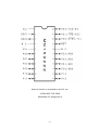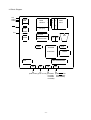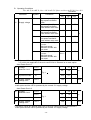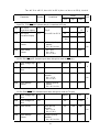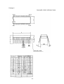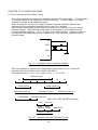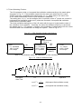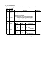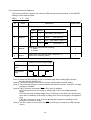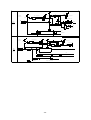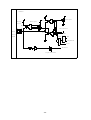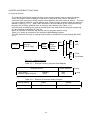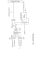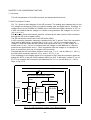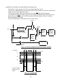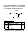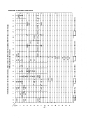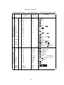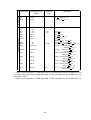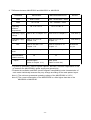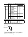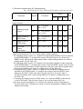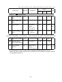
1
MICROCOMPUTER MN1500 MN150222/P0222 LSI User’s Manual Pub.No.20122-030E PanaXSeries is a trademark of Matsushita Electric Industrial Co., Ltd. The other corporation names,logotype and product names written in this book are trademarks or registered trademarks of their corresponding corporations. Request for your special attention and precautions in using the technical information and semiconductors described in this book (1) An export permit needs to be obtained from the competent authorities of the Japanese Government if any of the products or technologies described in this book and controlled under the "Foreign Exchange and Foreign Trade Law" is to be exported or taken out of Japan. (2) The contents of this book are subject to change without notice in matters of improved function. When finalizing your design,therefore,ask for the most up-to-date version in advance in order to check for any changes. (3) We are not liable for any damage arising out of the use of the contents of this book, or for any infringement of patents or any other rights owned by a third party. (4) No part of this book may be reprinted or reproduced by any means without written permission from our company. (5) This book deals with standard specifications. Ask for the latest individual Product Standards or Specifications in advance for more detailed information required for your design,purchasing and applications. If you have any inquiries or questions about this book or our semiconductors, please contact one of our sales offices listed at the back of this book or Matsushita Electronics Corporation's Sales Department. C o n tents CHAPTER 1 OVERVIEW 1.1 Overview 1.2 Features 1.3 Pin Assignment 1.4 Pin Descriptions 1.5 Unused Pins 1.6 Block Diagram 1.7 Electrical Characteristics 1.8 Package CHAPTER 2 CPU CORE FUNCTIONS 2.1 Clock Generator and CPU Basic Timing 2.2 ROM and RAM 2.3 Stack Area 2.4 Flag Status 2.5 Backup Mode 2.6 Reset 2.7 Clock Switching Function CHAPTER 3 I/O REGISTER FUNCTIONS 3.1 I/O Registers List 3.2 Allocation and Description of Registers 3.3 Available Instructions 3.4 Pin Structure Diagram CHAPTER 4 INTERRUPT FUNCTIONS 4.1 Interrupt Control 4.2 Interrupt Receiving Operation 4.3 Interrupt Return Operation 4.4 Stack upon Interrupt CHAPTER 5 TIMER FUNCTION CHAPTER 6 TIME BASE FUNCTION CHAPTER 7 A/D CONVERSION FUNCTION CHAPTER 8 AC ZERO VOLTAGE DETECTION FUNCTION CHAPTER 9 WATCHDOG TIMER FUNCTION CHAPTER 10 INSTRUCTION SETS CHAPTER 11 PRODUCT WITH ON-CHIP EPROM * This document is based on an equivalent Japanese document that was revised on Dec. 1999. -2- CHAPTER 1 OVERVIEW 1.1 Overview This is a high-performance, low power-consuming, 4-bit, single-chip CMOS microcomputer LSI with each 2-Kbyte ROM and 96-nibble RAM. For peripheral devices, the LSI incorporates a 10-bit A/D converter, AC zero voltage detection circuit, each 8-bit timer/counter, time base block, LED direct drive pin, Hi-Z output port control circuit, auto reset circuit and watchdog timer. The auto reset circuit and watchdog timer are mask optional functions. 1.2 Features [Hardware Features] ROM capacity : 2048 × 8 bits RAM capacity : 96 × 4 bits Instruction execution frequency: 1/8 fosc Machine cycle : 1.00 µs 1/8 × 8.00 MHz VDD=4.5 V to 5.5V 4.00 µs 1/8 × 2.00 MHz VDD=2.0 V to 5.5 V without auto reset circuit (VDD=VRSTL1 to 5.5 V with auto reset circuit) 8.00 µs 1/8 × 1.00 MHz VDD=1.8 V to 5.5 V without auto reset circuit (VDD=VRSTL1 or VRSTL2 to 5.5 V with auto reset circuit) Interrupt : 1 level (Software is selected with timer, time base, external interrupt or AC zero voltage detection interrupt.) Backup mode : STOP/HALT mode Timer/Counter : Timer/Event count function Time base : Time base and buzzer outputs function Watchdog timer : Resettable in approx. 33-ms cycle (at fosc=8.00 MHz) (Mask option) A/D converter : Max. 4-channel A/D conversion input, dividing into 1024 between VDD and VSS voltages AC zero voltage detection circuit: ACZ pin (shared with P31/IRQ) LED direct drive pin : 7 V (breakdown voltage) ×4 pins Auto reset circuit : VRSTL1 can be used when one machine cycle is 4 ms or more. VRSTL2 can be used when one machine cycle is 8 ms or more. (Mask option) I/O pins Hi-Z control : (Software selection) Pull-up resistor setting : (Mask option) I/O pin output type : (Push-pull or N-ch open-drain type) (Mask option) I/O pins: General-purpose I/O pins 15 pins A/D converter input Max. 4 pins (used in common with general-purpose I/O) Timer output/Buzzer output 1 pin (used in common with general-purpose I/O) IRQ/ACZ input 1 pin (used in common with general-purpose I/O) LED direct drive output 4 pins (N-ch open-drain output) (used in common with general-purpose input) SYNC pin/Timer input 1 pin (used in common with general-purpose I/O) Oscillator pin 2 pins Package : 20-pin SOP, 22-pin SDIP Process : Silicon gate CMOS [Software Features] - Total 51 instructions Direct addressing computation for all RAM areas Non-page program counter 4-/1-bit operational instructions -3- 1.3 Pin Assignment 20-PIN SOP TOP VIEW MN150222 Pin Assignment 1 -4- Note) No device is connected to the N.C. pin. 22-PIN SDIP TOP VIEW MN150222 Pin Assignment 2 -5- 1.4 Pin Descriptions Symbol Name I/O Function Initial State VDD VSS Power supply pins Apply +1.8 V to +5.5 V to VDD, and 0 V to VSS. OSC1 OSC2 Clock input Clock output I O Oscillator connection pins. A feedback resistor is built in. RST Reset input I/O The LSI is reset with low-level input into this pin. In order to reset the LSI without fail,it is recommendable to turn on low-level input into this pin for one machine cycle or more. The pin incorporates a Schmitt input circuit. The pull-up resistor connection is specified according to the mask option. Whenever reset input is cleared, the LSI waits for a certain period for the stabilization of oscillation. After that, the internal reset status of the LSI is cleared. This pin is used as an output pin of the mask optional auto reset circuit and watchdog timer circuit as well. P00 to P03 Parallel data I/O I/O 4-bit parallel data I/O ports. Output type is N-ch open-drain. Capable of directly driving the LED. Port input P10 to P13 Parallel data I/O I/O 4-bit parallel data I/O ports. Output type of N-ch open-drain or push-pull and a pull-up resistor connection can be specified by mask option. Port input P20/AD0 to P23/AD3 Parallel data I/O I/O (A/D converter (I) input) 4-bit parallel data I/O ports. Output type of N-ch open-drain or push-pull and a pull-up resistor connection can be specified by mask option. Each of these pins is switched in single-bit increments with software so that these pins will be available to A/D conversion input for a maximum of four channels. Port input -6- Symbol Name I/O Function Initial State CPU timing output at reset Port input after clearing reset P30 /SYNC /TCI Parallel data I/O I/O (Sync signal (O) output) (I) (Timer input) Parallel data I/O port. Output type of N-ch open-drain or push-pull and a pull-up resistor connection can be specified by mask option. The SYNC internal timing signal is output from this pin when the LSI is reset or within two machine cycles after the internal reset status of the LSI is cleared. The pin has push-pull output regardless of mask optional specifications while the SYNC timing signal is output. The TCI timer input pin incorporates a Schmitt input circuit. If the clock source of the timer is set to the TCI input with software, the output of P30/SYNC/TCI will be Hi-Z state. P31 /IRQ /ACZ Parallel data I/O I/O (External (I) interrupt) (I) (AC zero voltage input) Parallel data I/O port. The IRQ external interrupt pin incorporates a Schmitt input circuit. Output type of N-ch open-drain or push-pull and a pull-up resistor connection can be specified by mask option. The output of P31/IRQ/ACZ pin will be Hi-Z state if the external interrupt function or AC zero voltage detection interrupt function is selected with software. Parallel data I/O I/O (Timer output) (O) (Buzzer output) (O) Parallel data I/O port. Output type of N-ch open-drain or push-pull and a pull-up resistor connection can be specified by mask option. This pin is switched over with software so that timer or buzzer output from this pin will be enabled. P32 /TCO /BZ Port input Port input Note) The port input as an initial status described in the above table is applicable while the LSI is under Hi-Z control. After the Hi-Z status is cleared, each pin has output according to the mask option. -7- 1.5 Unused Pins It is recommendable to fix each unused pin to the status shown in the following table. Pin name Output type Pull-up resistor Fixation method P00 to P03 N-ch open-drain Selection disabled Fixed to "L" P10 to P13 N-ch open-drain ON OFF Open Fixed to "L" ON OFF Open N-ch open-drain P20/AD0 to P23/AD3 I/O port selection N-ch open-drain N-ch open-drain Fixed to "L" P30/SYNC/TCI N-ch open-drain N-ch open-drain ON OFF Open Fixed to "L" via a 1-kW resistor P31/IRQ/ACZ I/O port selection N-ch open-drain N-ch open-drain ON OFF Open Fixed to "L" P32/TCO/BZ I/O port selection N-ch open-drain N-ch open-drain ON OFF Open Fixed to "L" P10 to P13, P20 to CMOS push-pull Selection disabled (OFF) Open P23P30 to P32 I/O port selection Make the above settings, provided that the LSI is not under Hi-Z control. -8- 1.6 Block Diagram VDD OSC1 OSC2 CLOCK GEN. ROM 2048×8 I R LB Y S (4) P X (4) RAM 96×4 RST AUTO PC (11) RESET VSS INT.FLG HALT/ STOP ALU CF ZF INT.EN.FLAGF TMB A (4) SYSTEM CONTROL WDT TIMER A/D CONVERTER LB LB LB LB P0 P1 P2 P3 (P00 to P03) (P10 to P13) (P20/AD0 (P30/SYNC/TCI P21/AD1 P31/IRQ/ACZ P22/AD2 P32/TCO/BZ) P23/AD3) -9- Description of Block Diagram Block Instruction Execution Control Block Register Block Function IR ROM An instruction, which the CPU is about to execute, is read from the ROM and latched into the instruction register. The read only memory (ROM) is a program memory and stores a program to be run. PC The program counter is a 11-bit register which controls the execution sequence of the instructions in the program memory. See Note. SP The stack pointer (SP) is a 4-bit register indicating the address of the stack area which uses a part of the data RAM. The stack area is used to save the PC, etc. when a subroutine call or interrupt occurs. X X is a 4-bit register for indirect addressing of the RAM space. Y Y is a 4-bit register for indirect addressing of the RAM space. Arithmetic Block ALU The arithmetic and logic unit (ALU) performs arithmetic operations (addition, subtraction, increment, decrement and comparison) and logical operations (AND, OR, XOR, complement and rotate). Flag Block FS The flag status (FS) consists of two kinds of flags which indicate the running condition of the CPU. The carry flag (CF) is set when an ALU operation result either overflows or underflows. The zero flag (ZF) is set when an ALU operation result is zero, or otherwise, reset. (CF) (ZF) Data Memory Block RAM The random access memory (RAM) is used both as a stack area and a data area which accumulates the data required for running the program. Interrupt Control Block IF IE This block controls an interrupt using the interrupt control flag (IF) and interrupt enable flag (IE). Timer/Counter Block TM TB BC The timer/counter consists of TM which sets either the timer or event count mode and frequency dividing ratio, TB which sets a timer value and BC, a binary counter, which counts pulses. TMB The time base block divides the frequency of the clock signal fosc by the frequency dividing ratio selected with software. Time Base Block Note) Set the bits of the program counter as indicated below. (MSB) 10 9 8 PCh 7654 PCm (LSB) 3210 PCl - 10 - Block Function Oscillation Block CLOCK GENERATOR Connect a system clock oscillator between OSC1 and OSC2. Auto Reset AUTO RESET The auto reset function enables the low-voltage detection circuit to operate and sets the RST pin to low level when the VDD drops to or below VRSTL voltage. Watchdog Timer WDT The clock of fosc/212 is divided by 26 through the watchdog timer. The watchdog timer outputs a low-level signal to the RST pin if an overflow occurs. A/D Converter A/D The A/D converter has a resolution of 10 bits with a maximum of CONfour analog input channels. The analog input between the VDD VERTER and VSS voltages are divided by 1024 to convert the analog input into digital values. Others VSS VDD RST VSS and VDD are power supply pins. Apply +1.8 V to +5.5 V to VDD. RST is a reset pin and activated when the RST pin is at high level. - 11 - 1.7 Electrical Characteristics (See Note 1.) Type MOS LSI Function CMOS 4-bit single-chip microcomputer A. Absolute Maximum Ratings Ta = 25 °C VSS = 0 V Parameter Symbol Rating A1 Supply voltage VDD -0.3 to +7.0 V A2 Input clamp current (P31/IRQ/ACZ) IC -0.5 to +0.5 mA A3 Input pin voltage VI A4 Output pin voltage VO -0.3 to VDD +0.3 V A5 High-current output pin voltage VOH -0.3 to +7.0 V A6 I/O pin voltage VIO -0.3 to VDD +0.3 V A7 Peak output current (Other than P0) IOH(Peak) IOL(Peak) -10 20 mA A8 Peak output current (P0) IOL(Peak) 40 mA A9 Average output current (See Note 2.) (Other than P0) IOH(avg) IOL(avg) -0.3 to VDD +0.3 * Not applicable to P31/IRQ/ACZ Unit V -2 10 mA IOL(avg) 15 mA A11 Power dissipation PD See Note 3. mW A12 Operating ambient temperature Topr -40 to +85 °C A13 Storage temperature Tstg -55 to +125 °C A10 Average output current (See Note 2.) (P0) Note 1) Those electrical characteristics are reference values. For details, refer to the Product Standards. Note 2) Applied to any 100 ms period. Make sure that the total output current value of all output pins is 30 mA or less for 20-pin SOP and 50 mA or less for 22-pin SDIP. Note 3) 22-pin SDIP: PD = 350 mW 20-pin SOP : PD = 180 mW - 12 - B. Operating Conditions Ta = -40 °C to +85 °C, VDD = 1.8 V to 5.5 V (VRSTL1 or VRSTL2 to 5.5 V), VSS = 0 V See Note. Limits Parameter Symbol Conditions Unit min typ max B1 VDD1 Machine cycle: 1.0 µs High-speed oscillation mode 4.5 VDD2 Machine cycle: 4.0 µs High-speed oscillation mode without auto reset 2.0 5.5 VDD3 Machine cycle: 8.0 µs High-speed oscillation mode without auto reset 1.8 5.5 VDD4 Machine cycle: 64.0 µs Low-speed oscillation mode without auto reset 1.8 5.5 VDD5 Machine cycle: 4.0 µs or more High-/low-speed oscillation modes with auto reset VRSTL1 5.5 VDD6 Machine cycle: 8.0 µs or more High-/low-speed oscillation modes with auto reset VRSTL1 VRSTL2 5.5 Supply voltage 5.0 5.5 V Note) VRSTL1 and VRSTL2 voltages refer to the supply voltages that are detected to reset the LSI, which are applicable if the auto reset circuit is selected as a mask option. Auto Reset Circuit 1 B2 Voltage detection level VRSTH1 3.1 VRSTL1 2.0 3.0 VH 0.05 0.1 ∆ t/∆ V 1.00 4.0 V Fig. 1 B3 Hysteresis width B4 Supply voltage change rate ms/V * The above values are applied when use of the auto reset function is selected as a mask option and the LSI is operated by the normal 5-V supply voltage. Auto Reset Circuit 2 B5 Voltage detection level VRSTH2 2.0 VRSTL2 1.2 1.9 VH 0.05 0.1 ∆ t/∆ V 1.00 2.6 V Fig. 1 B6 Hysteresis width B7 Supply voltage change rate * The above values are applied when use of the auto reset function is selected as a mask option and the LSI is operated by the normal 3-V supply voltage. - 13 - ms/V Operating Speed Ta= -40 °C to +85 °C, VDD=1.8 V to 5.5 V (VRSTL1 or VRSTL2 to 5.5V), VSS=0 V Limits Parameter Symbol Conditions Unit min VDD=4.5 V to 5.5 V High-speed oscillation mode fosc=8.0 MHz tc1 B8 Instruction execution time tc3 tc4 Oscillation B9 Oscillator frequency max 1.0 VDD=2.0 V (VRSTL1) to 5.5 V High-speed oscillation mode fosc=2.0 MHz ( ): At auto reset ON tc2 typ µs 4.0 VDD=1.8 V(VRSTL1 or VRSTL2) to 5.5 V High-speed oscillation mode fosc=1.0 MHz ( ): At auto reset ON 8.0 VDD=1.8 V (VRSTL1 or VRSTL2) to 5.5 V Low-speed oscillation mode fosc=125 kHz ( ): At auto reset ON 64.0 OSC1, OSC2 (See Note.) fXtal1 VDD=1.8 V to 5.5 V High-speed oscillation mode 0.5 8.0 MHz fXtal2 VDD=1.8 V to 5.5 V Low-speed oscillation mode 32 125 kHz Note) OSC1 (Self-excited oscillation circuit) OSC2 C12 C11 VSS VSS - Have the sample of the above circuits evaluated by oscillator manufacturer to determine the external capacitance each of C11 and C12. In most cases, the appropriate value of each capacitor seems to be approx. 30 pF. - The LSI has an on-chip feedback resistor. - 14 - External Clock Input 1 OSC1 (High-speed oscillation mode. OSC2 is open.) Ta= -40 °C to +85 °C, VDD=1.8 V to 5.5 V (VRSTL1 or VRSTL2 to 5.5 V), VSS=0 V Limits Parameter Symbol Conditions Unit min B10 B11 max Clock frequency fosc1 High-level pulse width * twh1 Low-level pulse width * twl1 Rise time twr1 20 Fall time twf1 20 Input voltage high level VIH1 Input voltage low level VIL1 External Clock Input 2 1.0 typ Fig. 2 A clock duty ratio should be 45 % to 55 %. Fig. 2 8.0 MHz 40 40 ns 0.8VDD VDD VSS 0.2VDD V OSC1 (Low-speed oscillation mode. OSC2 is open.) Clock frequency fosc2 32 High-level pulse width * twh2 Low-level pulse width * twl2 Rise time twr2 20 Fall time twf2 20 Input voltage high level VIH2 Input voltage low level VIL2 Fig. 3 A clock duty ratio should be 45 % to 55 %. Fig. 3 - 15 - 125 MHz 0.8 0.8 ns 0.8VDD VDD VSS 0.2VDD V External Clock Input 3 TCI Ta= -40 °C to +85 °C, VDD=1.8 V to 5.5 V (VRSTL1 or VRSTL2 to 5.5 V), VSS=0 V Limits Parameter Symbol Conditions Unit min B12 Clock frequency typ ftci max 5 MHz VDD = 1.8 V to 5.5 V High-level pulse width * twh3 Low-level pulse width * twl3 Clock frequency ftci 100 Fig. 4 ns 100 2.5 MHz VDD = VRSTL to 1.8 V High-level pulse width * twh3 Low-level pulse width * twl3 Rise time trcp Fall time tfcp 200 Fig. 4 200 ns 20 20 Fig. 4 Input voltage high level VIH3 Input voltage low level VIL3 0.8VDD VDD V VSS 0.1VDD VDD VRSTH VH VRSTL Approx. 1V t Operating mode The status of Indefinite general-purpose Hi-Z port Indefinite Hi-Z VH : hysteresis width "L" Reset cleared "L" The status Indefinite of RST pin Fig. 1 Auto Reset Voltage - 16 - Indefinite 0.8 VDD 0.2 VDD twh1 twl1 twr1 twf1 fosc1 Fig. 2 OSC1 Timing Chart 0.8 VDD 0.2 VDD twh2 twl2 twr2 twf2 fosc2 Fig. 3 OSC1 Timing Chart 0.8 VDD 0.1 VDD twh3 twl3 trcp tfcp ftci Fig. 4 TCI Timing Chart - 17 - C. Electrical Characteristics (DC Characteristics) Ta= -40 °C to +85 °C, VDD=1.8 V to 5.5 V (VRSTL1 or VRSTL2 to 5.5 V), VSS=0 V Limits Parameter Symbol Conditions Unit min typ max Supply Current C1 C2 Operating supply current IDD1 fosc = 8.0 MHz VDD = 5.0 V 4.0 8.0 IDD2 fosc = 2.0 MHz VDD = 3.0 V 1.2 2.5 IDD3 fosc = 32.768 kHz VDD = 5.0 V 30.0 fosc = 32.768 kHz VDD = 5.0 V 15.0 mA 60.0 Supply current in HALT mode IDD4 30.0 C3 Supply current in STOP mode IDD5 VDD = 5.0 V 0.5 5.0 C4 Auto reset current consumption IDD6 VDD = 5.0 V 30.0 80.0 µA * Make measurement at Ta = 25 °C while under no-load condition. * To measure the operating supply current, IDD1, fix the I/O pins to VDD level in the RESET mode, input an 8-MHz square wave, which swings between VDD and VSS voltage levels, into the OSC1 pin. * To measure the operating supply current, IDD2, fix the I/O pins to VDD level in the RESET mode, input a 2-MHz square wave, which swings between VDD and VSS voltage levels, into the OSC1 pin. * To measure the operating supply current, IDD3, clear the reset mode and fix the I/O pins to VDD level during execution of NOP instruction, input a 32.768-kHz square wave, which swings between VDD and VSS voltage levels, into the OSC1 pin. * To measure the supply current in HALT mode, IDD4, clear the RESET mode and set to the HALT mode, and, after fixing the I/O pins to VDD level, input a 32.768-kHz square wave, which swings between VDD and VSS voltage levels, into the OSC1 pin. * To measure the supply current in STOP mode, IDD5, clear the RESET mode and set to the STOP mode. Then fix the I/O pins to VDD level and open OSC1 pin. * Auto reset current consumption,IDD6, refers to the constant current consumption of the auto reset circuit with the auto reset function ON selected as a mask option. Therefore, the value of current consumption is added to each supply current rating if the auto reset circuit is enabled. - 18 - Ta= -40 °C to +85 °C, VDD=1.8 V to 5.5 V (VRSTL1 or VRSTL2 to 5.5 V), VSS=0 V Limits Parameter Symbol Conditions Unit min High-Current I/O Pins C5 VIH1 C6 Input voltage low level VIL1 C7 Output leakage current OLK1 Output: Hi-Z VIN =0 V to 6 V C8 Output voltage low level VOL1 IOL =20.0 mA VDD =5.0 V C9 0.7VDD VDD V VSS 0.3VDD VSS ±10 µA 2.0 V P10 to P13 P20/AD0 to P23/AD3 (When the pins are used as P20 to P23 pins) P30/SYNC/TCI, P31/IRQ/ACZ, P32/TCO/BZ (When the pins are used as P30/SYNC, P31, P32/TCO/BZ pins) Input voltage high level VIH2 C10 Input voltage low level VIL2 C11 Input current II2 0.7VDD VDD V C12 Input leakage current C13 Output voltage high level VOH2 Output voltage low level VOL2 C14 max P00 to P03 (N-ch open-drain) Input voltage high level I/O Pins typ ILK2 VSS With pull-up resistor VIN = 1.5 V VDD = 5.0 V -50 0.3VDD -120 -300 µA Without pull-up resistor VIN = 0 V to VDD ±1 IOH = -500 µA VDD = 5.0 V 4.5 IOL = 3.5 mA VDD = 5.0 V VSS VDD V 0.5 Note) Use the P30/SYNC/TCI pin under the following condition: The load must be set so that the output voltage high level will be more than 0.8 VDD while the SYNC timing signal is output. That is, at the time the LSI is reset or within two machine cycles after the reset status of the LSI is cleared. - 19 - Ta= -40 °C to +85 °C, VDD=1.8 V to 5.5 V (VRSTL1 or VRSTL2 to 5.5 V), VSS=0 V Limits Parameter Symbol Conditions Unit min typ max Input Pins P20/AD0 to P23/AD3 (When the pins are used as A/D input pins) C15 Converted voltage range C16 Resolution C17 Relative precision C18 Zero transition voltage V0T C19 Full-scale transition voltage VFST C20 A/D conversion time C21 VAD VDD = 5.0 V VSS = 0.0 V Analog input voltage C23 Analog input leakage current C24 Ladder resistance VDD V 10 bit ±3 10 LSB 30 mV Sampling time C22 VSS VDD -10 VDD -30 fosc = 8 MHz VDD = 5.0 V VSS = 0.0 V 15.00 See Note. fosc = 8 MHz VDD = 5.0 V VSS = 0.0 V 5.00 See Note. µs VDD V ±.001 ±1 µA 50 100 kΩ VADIN 27.00 17.00 VSS VADIN= 0 V to VDD (VADIN when channel is off.) Rladd 10 µs Note) The value is applied when bp3 (ADTC) of the A/D control register ADCL is set to zero. Relative precision: The deviation of the converted straight line from the ideal straight line that results after both the zero transition voltage and full-scale transition voltage are adjusted to zero. Zero transition voltage: Indicates the difference between the analog input voltage and the nominal value when the digital output code changes from 0 (000h) to 1 (001h). Full-scale transition voltage: Indicates the difference between the analog input voltage and the nominal value when the digital output code (3FEh) reaches the full-scale value (3FFh). - 20 - Ta= -40 °C to +85 °C, VDD=1.8 V to 5.5 V (VRSTL1 or VRSTL2 to 5.5 V), VSS=0 V Limits Parameter Symbol Conditions Unit min typ max Input Pin P31/IRQ/ACZ (When this pin is used as ACZ pin) C25 ACZ input (high-level output) VSH ACZ input (low-level output) VSL 1.5 VDD -1.5 VSS 0.5 VDD -0.5 VDD Fig. 5 V C26 C27 C28 Input leakage current ILK3 Input clamp current IC3 VDD=4.5 V to 5.5 V Without pull-up resistor VIN = 0 V to VDD ±1 µA VIN > VDD VIN > VSS VDD = 5.0 V ±400 I/O Pin P31/IRQ/ACZ (Schmitt input when this pin is used as IRQ pin) C29 Input voltage high level VIH4 0.8VDD VDD C30 Input voltage low level VIL4 VSS 0.1VDD C31 Input current II4 V C32 Input leakage current ILK4 With pull-up resistor VIN = 1.5 V VDD = 5.0 V -50 -120 -300 µA Without pull-up resistor VIN = 0 V to VDD ±1 I/O Pin P30/SYNC/TCI (Schmitt input when this pin is used as TCI pin) C33 Input voltage high level VIH5 0.8VDD VDD C34 Input voltage low level VIL5 VSS 0.1VDD C35 Input current II5 V C36 Input leakage current ILK5 With pull-up resistor VIN = 1.5 V VDD = 5.0 V Without pull-up resistor VIN = 0 V to VDD - 21 - -50 -120 -300 µA ±1 Ta= -40 °C to +85 °C, VDD=1.8 V to 5.5 V (VRSTL1 or VRSTL2 to 5.5 V), VSS=0 V Limits Parameter Symbol Conditions Unit min I/O Pin typ max RST (Schmitt input) C38 Input voltage high level VIH6 0.8VDD VDD C39 Input voltage low level VIL6 VSS 0.1VDD C40 Input current II6 V With pull-up resistor VIN = 1.5 V VDD = 5.0 V C41 Input leakage current ILK6 Without pull-up resistor VIN = 0 V to VDD C42 Output voltage low level VOL6 VDD = 2 V, IOL = 0.3 mA - 22 - -50 -120 -300 µA ±1 VSS 0.4 V D. Electrical Characteristics (AC Characteristics) Ta= -40 °C to +85 °C, VDD=1.8 V to 5.5 V (VRSTL1 or VRSTL2 to 5.5 V), VSS=0 V Limits Parameter Symbol Conditions Unit min typ max RST Pin D1 Effective pulse width twRST Fig. 5 1 mc * The above pin may not be reset if the pulse width is shorter than the effective pulse width. (mc: Machine cycle) P31/IRQ/ACZ (When this pin is used as ACZ pin) Rise time D2 trs 30 Fig. 6 Fall time D3 tfs 30 0.8 VDD twRST 0.1 VDD Fig. 5 RST Input Pulse Width (Input) trs tfs VDD VSL VSH VSL VSS (Output) Fig. 6 AC Zero Voltage Detection Circuit Operating Diagram - 23 - µs 1.8 Package Package 1 PACKAGE CODE: SOP020-P-0300 - 24 - Package 2 PACKAGE CODE: SDIP022-P-0300 - 25 - Mask Option Check List Part No. MN150222 1. Operating supply voltage range Operating voltage range 2. Clock Usage Used Operating mode V to V HALT mode V to V STOP mode V to V ---- Oscillatio n mode Xtal Unused ---- 32 kHz to 125 kHz in low-speed oscillation mode Oscillator frequency 0.5 MHz to 8 MHz in high-speed oscillation mode Remarks 3. Auto reset function * Use the LSI in auto reset function ON mode with one machine cycle set to 4.0 ms or more when VRSTL1 reset voltage is selected and 8.0 ms or more when VRSTL2 reset voltage is selected. Auto reset function ON Reset voltage OFF Mark "P" on the corresponding item if ON is selected. 4. Pull-up resistor at reset pin ON VRSTL2 2.0 V to 4.0 V (Use the LSI at normal 5-V supply voltage.) 1.2 V to 2.6 V (Use the LSI at normal 3-V supply voltage.) 5. Watchdog timer function OFF ON 6. A/D conversion function ON VRSTL1 OFF 7. AC zero voltage detection function OFF ON - 26 - OFF 8.1 Pin Structure Pin name Function Output type selection N-ch open-drain Push-pull Pull-up resistor ON OFF Output type selection N-ch open-drain Push-pull Pull-up resistor ON OFF Output type selection N-ch open-drain Push-pull Pull-up resistor ON OFF Output type selection N-ch open-drain Push-pull Pull-up resistor ON OFF Output type selection N-ch open-drain Push-pull Pull-up resistor ON OFF Output type selection N-ch open-drain Push-pull Pull-up resistor ON Output type selection N-ch open-drain Push-pull Pull-up resistor ON OFF Output type selection N-ch open-drain Push-pull P10 P11 P12 P13 P20 P20/AD0 Note 1) AD0 P OFF P21 P21/AD1 Note 1) AD1 Pull-up resistor ON P OFF Output type selection N-chopen-drain Push-pull Pull-up resistor ON OFF Output type selection N-ch open-drain Push-pull Pull-up resistor ON Output type selection N-ch open-drain Push-pull Pull-up resistor ON OFF Output type selection N-ch open-drain Push-pull Pull-up resistor ON P22 P22/AD2 AD2 P OFF P23 P23/AD3 Note 1) AD3 P OFF Note 1) A pull-up resistor cannot be connected to the pin when AD pin is selected on PTAD2-0 of ADCH X 'A' , A/D Control Register. - 27 - 8.2 Pin Structure Pin name Function Output type selection N-ch open-drain Push-pull Pull-up resistor ON OFF Output type selection N-ch open-drain Push-pull Pull-up resistor ON OFF Output type selection N-ch open-drain Push-pull Pull-up resistor ON OFF P30/SYNC/TCI P31/IRQ/ACZ Note 2) P32/TCO/BZ Note 2) A pull-up resistor cannot be connected when the AC zero voltage detection function is used. - 28 - CHAPTER 2 CPU CORE FUNCTIONS 2.1 Clock Generator and CPU Basic Timing This LSI incorporates the system clock oscillation circuits (OSC1 and OSC2). The circuit has an oscillation element and capacitors connected externally. A Xtal oscillator or a ceramic oscillator is utilized as the oscillation element. When mounting the LSI on PCB, design a pattern so that the oscillation elements and capacitors will be arranged as physically close to the LSI as possible. Also provide a thick ground line that can be connected to VSS with the LSI at the shortest distance possible. Note that long wiring pattern is susceptible to noise interference and results in unstable oscillation. Fig. 2.1.1 shows a connection diagram. Optimum values for the capacitors differ depending on the oscillator used. Use the values specified by each oscillator maker. VSS OSC1 OSC2 VDD Fig. 2.1.1 Oscillation Circuit Connection Diagram This LSI constitutes a machine cycle (state) with 4-phase clocks, S0, S1, S2 and S3, generated from the oscillation source (OSC1 and OSC2). One machine cycle is 1.0 µs when oscillation source, fosc, is 8.0 MHz. Machine Cycle S3 S0 S1 S2 S3 Fetch Cycle n Execution Cycle n-1 ROM Read S0 S1 Fetch Cycle n+1 Execution Cycle n Execution Cycle n+1 Instruction Decode (JMP, CALL, RET and RETI interrupts) PC+1 PC Load RAM RAM Address Read SP-1 RAM Write SP+1 Fig. 2.1.2 Machine Cycle and CPU Basic Timing - 29 - 2.2 ROM and RAM This LSI has a 2-Kbyte instruction memory space (ROM) to store instructions, and a 96-nibble (including a 32-nibble stack area) data memory space (RAM) to store data separately from each other. Fig. 2.2.1 shows the ROM address space and Fig. 2.2.2 shows the RAM address space. Interrupt sources RESET 000 Interrupt Vector 00A IRQ 00C Interrupt Vector User Program (incorporated in ROM) RESET IRQ X '000' X '00A' * IRQ factor is set with software selection. timer, time base, external interrupt, or AC zero voltage detection interrupt 7FF Fig. 2.2.1 ROM Address Space Lower Address F E DCBA 9 8 7 6 5 4 3 2 1 0 Upper Address 0 1 2 3 4 5 6 7 Data Area Not used Stack Area Fig. 2.2.2 RAM Address Space - 30 - 2.3 Stack Area This LSI has assigned as a stack area the addresses (6, 0) to (7, F) in the RAM area. The stack area is used to save the PC (Program Counter), flag statuses (ZF and CF) and A, X and Y registers at the time of the CALL instruction, PSH instruction or an interrupt. When the entire stack area is not used, it is also available as regular RAM. When only the CALL instruction is executed, up to 8 levels can be used. Fig. 2.3.1 shows the stack condition when the CALL instruction, PSH instruction or an interrupt sequence is executed. (Odd-number Address) (Address) 3 2 1 0 (Even-number Address) 3 2 1 0 71-70 73-72 75-74 77-76 PCm CF After execution of interrupt LI FF ZF 79-78 PC1 PCh X 7B-7A 7D-7C 7F-7E PCm CF ZF LI FF Y After execution of PSHXY instruction A After execution of PSHEA instruction PC1 After execution of CALL instruction PCh Fig. 2.3.1 Stack Area Condition Note 1) At reset time, the SP (Stack Pointer) points to 60. The stack data are used sequentially, starting at address 7F to 60. Note 2) The RET instruction does not return the flags (CF, ZF and LIFF). Only the RETI instruction is returned. Note 3) LIFF: This is FF to memorize that the instruction just before was LI. It is used for an LI instruction stacking function. Note 4) The values in the oblique-lined cells in Fig. 2.3.1 are indefinite. - 31 - 2.4 Flag Status The flag status is composed of a 2-bit register consisting of the arithmetic flags, that is, carry flag (CF) and zero flag (ZF). CF is set when an arithmetic result of the ALU overflows or underflows, or is otherwise reset. ZF is set when the arithmetic result of the ALU is zero, or is otherwise reset. 2.5 Backup Mode In order to reduce power consumption, there are two kinds of backup modes provided, which can be controlled by the program. - HALT mode: The system clock frequency divider is operating. However, system clock is not supplied. It is returned by a reset operation or an interrupt. - STOP mode: The power consumption can be reduced further because the system clock frequency divider is also stopped. As with the HALT mode, it is returned by a reset operation or an interrupt. (Software option) Table 2.5.1 shows the STOP and HALT functions. Table 2.5.1 STOP and HALT Functions Mode Operation Operating condition STOP HALT 1) The system clock oscillation circuit stops. 1) The system clock oscillation circuit is operating. (System clock frequency divider is operating. However, system clock is not supplied.) 2) Timer/Counter - It is operating in event count mode. - It is stopped in timer mode. 2) Timer/Counter - It is operating in event count mode. - It is operating when the clock is 14 fosc/2 in timer mode. - It is operating when the clock is fsys/2 in timer mode. 3) Time base is stopped. 3) Time base is operating. Register/RAM condition Holds the contents of the RAM and all registers. Mode setting method Executes a WI instruction just after an EDI instruction. (Refer to Example: 2.5.1.) Return Executes the WI instruction after an instruction other than an EDI instruction. (Refer to Example: 2.5.2.) - Interrupt: Identical operation with a normal interrupt - Reset : Identical operation with a normal reset Example: 2.5.1 Using the STOP Mode ED 0.4 WI NOP Exits from the STOP mode when an IRQ (external interrupt) occurs. Be sure to insert one or more NOPs next to the EDI and WI instructions in order to stabilize operation. Note) Following is an interrupt which enables return from the STOP mode. IRQ (External interrupt, ACZ interrupt or timer in the event count mode.) - 32 - Example: 2.5.2 Using the HALT Mode EDI 0.4 Returns from the HALT mode when an interrupt occurs. (Instruction other than EDI instruction) WI NOP Note) Be sure to insert one or more NOPs next to the WI instruction. The currently provided cross assembler inserts an NOP automatically. Table 2.5.2 shows the comparison of STOP and HALT modes. Table 2.5.2 STOP and HALT Modes Comparison Table OSC IRQ CPU RESET STOP mode - P (Note 1) - P HALT mode P P (Note 2) - P P : Operates - : Stops Unless the MASKIR bit is set to zero, IRQ does not operate. Note 1) The timer interrupt function operates in event count mode and does not operate in timer mode. The time base interrupt function does not operate in STOP mode. Note 2) The timer interrupt function operates in event count mode or timer mode with the clock source of fosc/214 selected but does not operate in timer mode with the clock source of fsys/2 selected. The time base interrupt function, however, operates. - 33 - Precautions for using the Backup Mode 1. Handling of the output ports In the backup mode, the port level can be made floating in order to reduce power consumption at the output ports. The port status can be set by controlling the corresponding bit of the control register. (Refer to Table 2.5.3.) Table 2.5.3 Interrupt Mode Register (CPUM: X'4' R/W) versus Output Ports HIZC Port Status 1 All output pins are floating (Hi-Z) Note) The voltage level is set to "H" if a pull-up resistor is selected as a mask option. 0 Normal output (Set to "1" in RESET mode) 2. Handling of the input ports A pull-up resistor for the input port should be specified according to the external circuit voltage level in the backup operation, in order to reduce power consumption at the port. Set the input port voltage level externally so that it will be turned to either "L" or "H" level in the backup operation. When the port is at the middle level, a current flows internally and the microcomputer consumes more power. 3. Return from the STOP mode When the supply voltage is less than 1.8 V at the time of return, the RAM data cannot be guaranteed after return. If this is the case, reset by means of an external circuit or use the auto reset function. 4. Handling of the I/O ports After first setting to the Hi-Z state, set the I/O ports externally so that the pin levels will be turned to "L" or "H" level. When they are at the middle level, the microcomputer consumes more power. 5. Handling of the A/D Control Registor Setting from outside is not needed when A/D input is unused on AD, because P2 input gate is fixed to stop feedthrough current. The pin which selects AD cannot be connected to a pull-up resistor as a mask option. - 34 - 2.6 Reset The LSI is reset with the RST pin set to "L" level. When the LSI is reset, the register and output port latch are initialized as shown in table 2.6.1. The RST pin should be set to "L" level for a machine cycle or more for stabilized reset operation, otherwise the LSI may not be reset. Table 2.6.1 Initial Values of Registers and Data Memories Register/Memory Symbol Initial Value Program counter PC P Accumulator A P Register X X P Register Y Y P Carry flag CF P Zero flag ZF P Register/Memory Interrupt accept flag Interrupt enable/disable flag Symbol IF P IE Disabled Output port latch I/O register RAM Stack pointer Initial Value 1 IR 1 Indefinite SP 60 [Reset Clearing Timing] 14 7 This LSI clears an internal reset by counting 2 pulses (2 pulses in low-speed mode) worth of OSC input clock after the RST pin is turned to "H". This is because the microcomputer may malfunction if a reset is cleared when the oscillation source of system clock is unstable. When designing a system, design the reset timing taking the above point into account. Refer to Fig. 2.7.2. - 35 - 2.6.1 Auto Reset Function (Mask Option) The auto reset circuit is enabled or disabled according to the mask option. The auto reset function enables the low-voltage detection circuit to operate and sets the RST pin to "L" level when the VDD drops to or below VRSTL level. The following diagram shows the auto reset block. VDD Pull-up resistor Mask option RST Reset delay circuit Internal reset VDD Mask option N-ch O R Low-voltage detection circuit (reset voltage at 2.0 V to 4.0 V) Low-voltage detection circuit (reset voltage at 1.2 V to 2.6 V) Watchdog timer Mask option - 36 - 2.7 Clock Switching Function The LSI operates in high- or low-speed Xtal oscillation mode according to the mask option. As shown in Fig. 2.7.1, the oscillation starts from the reset cycle when the LSI is reset. At CPU reset time, a hardware-wise waiting time, twait (osc), takes place in the return from STOP mode automatically until the clock oscillation is stabilized. The waiting time, twait (osc), on the oscillator side is a period in which 214 pulses are counted in high-speed Xtal oscillation mode and 27 pulses are counted in low-speed Xtal oscillation mode after the oscillation starts. The clock oscillation starting time of the LSI varies with the type of crystal and the value of the oscillation circuit capacitor. Generally, the lower the oscillator frequency is, the slower the starting time is. For example, it requires a few hundreds of milliseconds at 32 kHz, which should be taken into consideration to design the system. Refer to Fig. 2.7.1. Fig. 2.7.1 CPU Operation Modes and Settings Reset HALT fosc: Oscillates 1/8 fosc mode CPU stops WI Interrupt Reset Cleared (Note 1) EDI NORMAL WI fosc: Oscillates 1/8 fosc mode fosc: operates Interrupt (Note 1) STOP fosc: Stops 1/8 fosc mode CPU stops Note 1) The hardware awaits the stabilization of OSC oscillation. Fig. 2.7.2 Wait at Oscillation Start Oscillation Start Time twait Operation twait=214 × 1 fosc (High-speed Xtal oscillation mode) twait=27 × 1 fosc (Low-speed Xtal oscillation mode) - 37 - CHAPTER 3 I/O REGISTER FUNCTIONS 3.1 I/O Registers List Address Name Function X'0' PORT0 P0 port register X'1' PORT1 P1 port register X'2' PORT2 P2 port register X'3' PORT3 P3 port register X'4' CPUM CPU control X'5' TBL Timer control (Timer buffer lower 4 bits) X'6' TBH Timer control (Timer buffer upper 4 bits) X'7' TM Timer control (Timer mode) X'8' TMBC Time base control X'9' ADCL A/D control X'A' ADCH A/D control X'B' ADDL A/D control (A/D buffer lower 2 bits) X'C' ADDM A/D control (A/D buffer middle 4 bits) X'D' ADDH A/D control (A/D buffer upper 4 bits) X'E' Not used X'F' IRQC Interrupt selection - 38 - 3.2 Allocation and Description of Registers 3.2.1 I/O Port Registers Data output to the pin is done by writing the output data into the port register, and data input from the pin is done by reading the data from the port register. Each register consists of 4 bits (one port worth). Address Name Port I/O Description X'0' PORT0 P0 I/O 4-bit parallel data I/O port. The output is N-ch open-drain type. Capable of directly driving the LED. X'1' PORT1 P1 I/O 4-bit parallel data I/O port. The output type and a pull-up resistor connection can be specified by a mask option. X'2' PORT2 P2 I(P20) I/O 4-bit parallel data I/O port. The P20 to P23 are used in common with AD0 to AD3 respectively. The output type and a pull-up resistor connection can be specified by a mask option. X'3' PORT3 P3 I/O 4-bit parallel data I/O port. The P30 is shared with the SYNC and TCI (timer input). The P31 is shared with the IRQ and ACZ. The P32 is shared with the TCO (timer output) and BZ (buzzer) output. 3.2.2 CPU Control Register The Hi-Z control of all I/O pins is specified through the CPU control register. So are the control of the watchdog timer operation and the system clock frequency dividing ratio. CPUM X '4' bit Name 0 HIZC 1 WDEN R/W (bit 1 is write-only.) Description Initial Value Specifies Hi-Z for all output pins. See Note 1. 1: Sets all the pins to Hi-Z. 0: Clears Hi-Z control for all the pins. 1 Specifies the operation of the watchdog timer. See Note 2. 1: Clear 0: Enabled 0 2 Always set to 1. 1 3 Unused Note 1) Hi-Z control does not apply to the SYNC pin and pull-up selection pin. Note 2) If WDEN is set to 1, the counter clear signal is output for one machine cycle. Then WDEN is set to 0 and the watchdog timer restarts, provided that the watchdog timer is selected as a mask option. - 39 - 3.2.3 Timer Control Registers This LSI incorporates an 8-bit timer. Address Name Configuration Function Initial Value X '5' TBL R/W Note) Timer buffer lower 4 bits F X '6' TBH R/W Note) Timer buffer upper 4 bits F X '7' TM R/W Timer mode register F X '8' TMBC R/W Time base mode register Indefinite Note) The value of the binary counter is read out at register read time. (1) Timer buffer This is a register to set the data to the timer binary counter. Since the value of the binary counter is read out at register read time, a value different from the written one may be read out while the timer is operating. TBL X '5' R/W bit Description 0 to 3 TBH bit 0 to 3 Timer buffer lower 4 bits X '6' Initial Value F R/W Description Timer buffer upper 4 bits Initial Value F - 40 - (2) Timer Mode Registers The timer mode register is used to set the clock source and operation mode of timer. TM X '7' R/W bit Name 0 TMEN 1 TCOE Description Initial Value Specifies timer operation. 1: The timer stops. 0: The timer operates. 1 Selects P32, TCO or BZ. (Selects port I/O, timer output or buzzer output.) 1: Selects P32/BZ (port I/O or buzzer output). 0: Selects TCO (timer output). Note) Selects P32 or BZ with bit 1 (BZOE) of the X'8' port register. 1 Selects the clock of timer. 2 3 CLK0 CLK0 CLK1 Clock Source 0 0 TCI input/26 See Note 1. 0 1 TCI input See Note 1. 1 0 fosc/214 1 1 fsys/2 See Notes 2 and 3. CLK1 1 1 Note 1) The P30/SYNC/TCI output is set to Hi-Z. Note 2) fsys = 1/8fosc. Note 3) If fsys/2 is selected, the timer stops when the LSI is in HALT mode. - 41 - 3.2.4 Time Base Control Register This LSI incorporates a time base besides an 8-bit timer. (1) Time Base Mode Register This register is used for the selection of time base output and clock source setting. TMBC X '8' R/W (bit 0 is read-only) bit Name 0 TMB 1 BZOE Description When the IN instruction is executed, the clock frequency, which is selected by the BZSEL0 and BZSEL1 bits, is set in bit 0 of the accumulator. Selects P32, TCO or BZ. 1: Selects P32. 0: Selects BZ (buzzer output). Note) The setting in the BZOE bit is disabled if TCO output is selected with the TCOE bit. Initial Value Indefinite 1 Selects clock output to be provided to the buzzer and time base. 2 3 BZSEL0 BZSEL1 BZSEL0 BZSEL1 1 1 fosc/212 1 0 fosc/211 0 1 fosc/210 0 0 fosc/29 - 42 - Clock Source 1 1 3.2.5 A/D Control Register This LSI incorporates a 4-channel A/D converter. The LSI uses a total of eight registers for channel selection, starting A/D conversion, or stopping A/D conversion. ADCL bit X '9' R/W Name Description Initial Value Selects the channel for A/D conversion. 0 1 ADCHS0 ADCHS1 ADCHS1 ADCHS0 Channel 1 1 AD0 1 0 AD1 0 1 AD2 0 0 AD3 1 1 2 ADSTAT Indicates the operation status of A/D conversion. 1: A/D conversion is completed or is not in process. 0: A/D conversion has started or is in process. 1 3 ADTC Selects the A/D conversion rate. 1: 15 machine cycles 0: 27 machine cycles 1 ADDH bit X 'A' R/W Name Description Initial Value Selects P20 to P23 or AD0 to AD3 signals. 0 PTAD0 1 PTA D0 1 2 PTAD1 PTA D1 Setting PTA D2 0 0 0 Selects AD0 to AD3 1 0 0 Selects AD0 to AD2 and P23 0 1 0 Selects AD0, AD1, P22 and P23 1 1 0 Selects AD0 and P21 to P23 * * 1 Selects P20 to P23 1 PTAD2 1 *: Don't care 3 ADHAL Disconnects the reference power supply in order to save the current consumption of the A/D converter. 1: A/D converter not in use. 0: A/D converter in use. 1 Note) When the A/D converter is in use, set the analog data input pins to analog data input only mode. On that occasion, the pin which selects AD cannot be connented to a pull-up resister. To set the LSI to low-current consumption mode (i.e., STOP or HALT mode), set the ADHALT bit to 1. - 43 - (1) A/D Buffer The following A/D buffers are used for storing the results of A/D conversion. ADDL bit 0 1 X 'B' R Name ADD0 ADD1 Description A/D conversion result Bits 1 and 0 (LSB) 2 Unused 3 Unused ADDM bit 0 1 2 3 ADDH bit 0 1 2 3 X 'C' ADD2 ADD3 ADD4 ADD5 Description A/D conversion result Bits 5 to 2 Initial Value Indifinite R Name ADD6 ADD7 ADD8 ADD9 Indifinite R Name X 'D' Initial Value Description A/D conversion result Bits 9 (MSB) to 6 - 44 - Initial Value Indifinite 3.2.6 Interrupt Selection Registers The interrupt selection registers are used for IRQ interrupt source selection, or the ON/OFF setting of each interrupt mask. IRQC bit 0 X 'F' R/W Name IRQSE0 Description IRQ interrupt source selection. See Note 1. IRQSE0 1 IRQSE1 2 MaskIR 3 IRQEC Initial Value 1 IRQSE1 0 0 Time base (See Note 2.) 0 1 Timer 1 0 ACZ (See Notes 4 and 5.) 1 1 IRQ (See Note 3.) 1 (See Note 5.) Selects the IRQ interrupt masking. 1: Mask 0: Permit Selects the IRQ interrupt edge. (See Note 1.) Refer to the following chart. 1 1 Selection of IRQ enabled edge IRQEC set value 1 0 IRQ enabled edge Note 1) Select the IRQ interrupt source or enabled edge after masking IRQ interrupt function with the MASKIR bit. Note 2) Time base interrupt occurs at the rising or falling edge of buzzer output. Note 3) Timer interrupt occurs in synchronization with a timer overflow. Therefore, no edge selection is enabled. Note 4) If ACZ interrupt is selected, IRQ or P31 input is disabled. ACZ interrupt occurs at the rising or falling edge of AC zero voltage detection output. ACZ interrupt uses an edge trigger circuit. Therefore, more than one interrupt may occur due to chattering if the rising or falling time of the input signal is comparative long. If the AC zero-cross is used, write an appropriate program for masking for the prevention of detection errors. Note 5) The P31 output is set to Hi-Z if the IRQ or ACZ input is used as an IRQ interrupt source. - 45 - IRQSE1 P31/IRQ/ACZ M P X IRQ interrupt Mask Edge selection M P X P30/SYNC/TCI M P X MASKIR IRQEC AC zero voltage detection Timer IRQSE0 Time base IRQSE1 P32/TCO/BZ 3.3 Available Instructions The following instructions can access the I/O registers. Addresses Available Instructions X '0' to X '4' X '7' to X 'A', X 'F' IN, OUT X 'B' to X 'D' IN X '5' to X '6' See Note 1. IN, OUT Note) The initial input of a register is indefinite and so is the input of the register while the LSI is in operation, if the register is not set up. Note 1) The binary counter value is read when the IN instruction is executed. - 46 - 3.4 Pin Structure Diagram The following shows the pin structure of this LSI. * I / O P in P u ll-u p r e s i s t o r P -ch M a sk o p tion RST RST M a sk o p tio n A u to reset output R e s e t v o l t a g e : 2 . 0 V to 4 . 0 V Auto reset output R e s e t v o l t a g e : 1 . 2 V to 2 . 6 V N -ch M a sk o p tion W a t c h d o g t im e r o u t p u t * I/O P i n s H i-Z c o n t r o l N -ch O u t p u t d a ta P00 to P03 D a ta b u s I n p u t i n s t r u c tio n - 47 - * I/O P ins M ask option P u l l - u p r e s i st o r P -ch M ask option P -c h P10 to H i-Z c o n tro l P13 N -c h O u t p u t d a ta D a ta b u s In p u t instructio n * I/O P ins P ull-u p r e s i st o r M a s k o p tio n M ask option P -ch P -c h H i-Z c o n tro l P20 /A D 0 to N -c h O u t p u t d ata P23 /A D 3 P T A D 0 to 2 D a ta b u s I n p u t i n s tructio n A /D in p u t d a ta - 48 - * I / O P in P u ll-u p resistor M a sk o p tion P -ch M a sk o p tion P -ch H i-Z c o n t r o l P30 CLK0 /S Y N C RST N -ch /T C I M P X S0 O utput data TCI D a ta b u s Inp ut instruction * I / O P in P u ll- u p resistor M a sk o p tio n M a sk o p tio n P -ch P -ch H i - Z c o n tr o l N -ch O u t p u t d a ta IR Q S E 0 P31 ACZ A C z ero voltage detection circuit /I R Q ( I n t e r r u p t) /A C Z IR Q ( I n t e r r u p t) IR Q S E 1 D a ta b u s IR Q S E 1 IR Q S E 0 Inp u t instruction - 49 - IR Q S E 0 * I/O P in M a s k o p t io n P-ch P u ll-u p M a sk o p tio n resisto r P -c h H i- Z c o n t r o l P32 N -c h BZOE /T C O TCOE /B Z M P X M P X BZ O u t p u t d a ta TCO D a ta b u s I n p u t in s tru ctio n - 50 - CHAPTER 4 INTERRUPT FUNCTIONS 4.1 Interrupt Control The interrupt control block breaks the flow of the running program with an interrupt request, saves the program status existing at break time to stack area, and controls the start of execution of an interrupt servicing program commensurate with each interrupt source. The user can use 4 kinds of interrupt sources except reset (These sources share the same first servicing address.) (See Fig. 4.1.1). With a JMP instruction, the first address of the interrupt servicing program can be freely specified from an interrupt start address (See Table 4.1.1). An interrupt is received by the interrupt control block only when both the interrupt request flag (IF) and interrupt enable flag (IE) are set. When an interrupt is received, the interrupt serving program starts running. Table 4.1.2 shows an example of the interrupt enable/disable program. The IRQ selects the source of interrupt and permits or prohibits the source through the IRQC (X'F'). Interrupt Maskable Interrupt (With IE Flag) Mack Circuit Interrupt Edge Control Circuit M P X IRQ M IRQ ACZ P X M P X Timer Time Base Fig. 4.1.1 Interrupt Sources Table 4.1.1 Interrupt Servicing Program Start Address Interrupt Source (CPU reset) External signal interrupt Vector Address (RESET) (IRQ) Priority 000 00A High Table 4.1.2 Example of Interrupt Setting Program Setting Method IRQ Enable EDI 0,4 - 51 - Disable EDI 4,0 4.2 Interrupt Receiving Operation When an interrupt source such as timer is generated, the program is branched to the top of the interrupt servicing program to receive an interrupt (See Fig. 4.2.1). When an interrupt source is generated, the interrupt request flag (IF) is set. When this is done, if the interrupt enable flag (IE) has been set, the generated interrupt source obtains the right to be received. Interrupt reception functions similarly to when a CALL instruction is executed. In the interrupt reception cycle, the program counter (PC) and flag status (FS) are written (pushed) in the stack area RAM. Next, the program counter (PC) is set in the specified interrupt servicing program start address. Then, the IE and IF are reset. As desired, use the JMP instruction from the interrupt servicing program start address to run each interrupt servicing program. Main Program 10 Main Program 11 Start of Interrupt Servicing Program Note 1) Main Program 12 Interrupt Program 1 Interrupt Program 2 Note 2) RETI Main Program 13 End of Interrupt Servicing Program Main Program 14 Main Program 15 Note 1) The interrupt program start address is set in the program counter (PC), and the PC and flag status (FS) values for the main program are pushed in the stack area. Note 2) The PC and FS values in the stack area are popped. Fig. 4.2.1 Interrupt Operation The following shows an example of the interrupt servicing program. Example) In case of IRQ Absolute Address 000A JMP LABEL: PSHXY PSHEA LABEL Interrupt Servicing Program POPEA POPXY EDI 0, 4 RETI - 53 - 4.3 Interrupt Return Operation A RETI (Return from Interrupt) instruction is used to return from execution of the interrupt servicing program to the original program. The RETI instruction functions similarly to a RET (Return) instruction which is used to return from a subroutine to a main routine. That is, by executing the RETI instruction, the values of the program counter (PC) and flag status (FS) just before an occurrence of an interrupt, pushed in the stack area RAM, are returned to the PC and FS, and the program flow existing before interrupt generation is restored. It takes 4 machine cycles to start an interrupt servicing program after an interrupt source is generated. When there is an EDI instruction in the top address of the interrupt servicing program, the interrupt is disabled for 3 to 4 machine cycles. 4.4 Stack upon Interrupt When receiving an interrupt or returning from it, the stack level changes by how much the program counter (PC) and flag status (FS) are pushed or popped. In the case of a normal interrupt, the 4-word stack area RAM is required because the PC and FS are pushed. Therefore, the value of the stack pointer (SP) is decremented by 4 upon receiving the interrupt and incremented by 4 upon returning from the interrupt (See Fig. 4.4.1). A return from interrupt is done by executing the RETI instruction. The RETI instruction restores the original values of the FS and PC which have been pushed in the stack area RAM during the interrupt reception cycle. The SP is incremented after reading out the values in the RAM indicated by SP. Address 61-60 Address 61-60 7B-7A 7B-7A 7D-7C PCm PCl 7D-7C 7F-7E FS PCh 7F-7E When Servicing the Interrupt When Returning from the Interrupt : Address value indicated by the stack pointer (SP) Fig. 4.4.1 Stack Pointer Operation - 54 - CHAPTER 5 TIMER FUNCTION As shown in Fig. 5.1.1, this LSI incorporates an 8-bit timer/counter and operates in timer mode or event count mode. To start the timer, execute the OUT instruction to set the desired time value in the timer buffer (TB) first and set the clock source in the timer control register (TM) next. Then the value in the timer buffer (TB) is transferred to the binary counter (BC) and the clock selected with the TM starts counting. When the BC overflows, the interrupt reception flag (IF) is set and the TB value is set again in the BC simultaneously, provided that the interrupt source of IRQ has been selected for the timer with software with the mask option cleared. The BC repeats the above-mentioned sequence unless the control mode is changed. 1. Timer Mode In timer mode, one of the following clocks is selected by the TM and the BC uses the one selected by the TM to start counting. (1) 1/2 fsys (fsys: internal clock) (2) 1/214 of OSC1 pin input pulse frequency 2. Event Count Mode In event count mode, one of the following clocks is selected by the TM and the BC uses the one selected by the TM to start counting. (1) TCI pin input pulse as it is (2) 1/26 of TCI pin input pulse frequency Refer to the specifications of external clock input 3 for the waveform of TCI input. P30 output is set to Hi-Z in event count mode with TCI input selected. Note) The BC value cannot be read at a single time but in the order of the upper bits and lower bits. Pay utmost attention to and take into consideration the timing that the BC value changes while reading it. - 55 - 5(6(7'(/$< IV\V &/. ; 3 0 &/. ; &LUFXLW $&= LQWHUUXSW UHTXHVW ,QWHUUXSW &RQWURO 3RUW LQWHUUXSW UHTXHVW 2XWSXW %X]]HU ; 7&2( %=2( 3RUW 2XWSXW 3 7LPH EDVH LQWHUUXSW UHTXHVW 5 3 &/. ; 3 ; 0 3 0 ELW %& 70(1 0 7% : 0 )LJ 7LPHU )XQFWLRQ 2SHUDWLRQ %ORFN 'LDJUDP IRVF 7&, %XV VKDUHG ZLWK $GGUHVV DQG 'DWD 25 ,1 ,54&25( +,= &/. 3RUW 2XWSXW +,= 36<1&7&, 37&2%= 3 1) The following shows the bit allocation of the timer control register (TM). TM X '7' R/W bit 0 1 Name TMEN TCOE Description Initial Value Specifies timer operation. 1: The timer stops 0: The timer operates 1 Selects P32, TCO or BZ. (Selects port I/O, timer output or buzzer output.) 1: Selects P32/BZ (port I/O or buzzer output) 0: Selects TCO (timer output) Note) Select P32 or BZ with bit 1 (BZOE) of the X '8' port register. 1 Selects the clock of timer. 2 CLK0 CLK0 CLK1 Clock Source 0 0 TCI input/26 See Note 1. 0 1 TCI input 1 See Note 1. 3 CLK1 1 1 0 fosc/214 1 1 fsys /2 See Notes 2 and 3. Note 1) The P30/SYNC/TCI output is set to Hi-Z. Note 2) fsys = 1/8 fosc. Note 3) If fsys/2 is selected, the timer stops when the LSI is in HALT mode. 2) Timer buffer (TB) setting method A timer buffer (TB) set value is obtained by the following expression. Set value = 256 - Desired counts (1 < Desired counts < 256) Example 1) Timer buffer (TB) set value when counting 100 times Set value = 256 - 100 = 156 = 9C (hex) - 57 - 5.1 Description of Timer Function Application Mode Timer Mode Registers CLK1 TB Set Value Output Frequency CLK0 Timer mode (fosc=4.19 MHz) 0 1 80 C0 E0 F0 1 2 4 8 Hz(1s) Hz(0.5 s) Hz(0.25 s) Hz(0.125 s) Event mode (ftci=32.768 kHz) 0 0 00 80 C0 E0 1 2 4 8 Hz Hz Hz Hz Timer mode (fosc=4.19 MHz) 1 1 80 C0 1.024 kHz 2.048 kHz Timer mode (fosc=4.0 MHz) 1 1 80 C0 0.976 kHz 1.953 kHz Event mode (ftci=32.768 kHz) 1 0 F0 F8 1.024 kHz 2.048 kHz Timer mode (fosc=4.0 MHz) 1 1 Clock BZ Table 7.2.1 Melody frequencies (example) Sound n* Melody C7 Do C7 D7 Re D7 E7 Mi F7 Fa F7 G7 So G7 A7 La A7 B7 Si C8 Do 60 57 54 51 48 45 43 40 38 36 34 32 30 TB set value Output frequency (Hz) Tempera- C4 C7 CA CD D0 D3 D5 D8 DA DC DE E0 E2 2083.3 2192.9 2314.8 2451 2604.2 2777.8 2907 3125 3289.5 3472.5 3676.5 3906.3 4166.7 2093 2217 2349.3 2489 2637 2793.8 2960 3136 3322 3520 3729 3351.1 4186 ment scale (Hz) *n = number of desired counts - 58 - CHAPTER 6 TIME BASE FUNCTION As shown in Fig. 6.1.1, this LSI has a function to output clock signals that are generated by dividing the frequency of oscillation source to the pin or accumulator. Furthermore, by selecting time base interrupt with the IRQC in software control, the output can be used as an interrupt source. Right after the P32/TCO/BZ pin is set to buzzer output, the initial buzzer output value, the period until the first output signal's rising edge, or the period until the signal's falling edge is indefinite or not guaranteed. The following table shows the bit allocations of the time base control register (TMBC). TMBC X '8' R/W (Bit 0 is read-only) bit Name 0 TMB 1 BZOE Description When the IN instruction is executed, the clock value, which is obtained by dividing the frequency of oscillation source by the BZSEL0 signal and BZSEL1 signal, is set in bit 0 of the accumulator. Selects P32, TCO or BZ. 1: Selects P32 0: Selects BZ (buzzer output) Note) The setting in the BZOE bit is disabled if TCO output is selected with the TCOE bit. Initial Value Indefinite 1 Selects clock output to be provided to the buzzer and time base. 2 BZSEL0 BZSEL0 3 BZSEL1 BZSEL1 Clock Source 1 1 fosc/212 1 0 fosc/211 0 1 fosc/210 0 0 fosc/29 - 59 - 1 1 CHAPTER 7 A/D CONVERSION FUNCTION 7.1 Overview This LSI incorporates a 10-bit A/D converter and sample-and-hold circuit. 7.2 A/D Conversion Function Fig. 7.2.1 shows a block diagram of the A/D converter. The analog input between the VDD and VSS voltages are divided by 1024 to convert the analog input into digital values. Therefore, VIN voltage input into the P20/AD0 to P23/AD3 pins is converted into digital values for X '3FF' to X '000' on condition that the voltage VIN is within a range between the voltages VSS and VDD. (VDD > VIN > VSS) A/D conversion starts with channel selection, followed by the start control of A/D conversion through the A/D control register (ADC). The A/D conversion result is set in the A/D buffer (ADD). In A/D conversion operation, sampling is performed for the Ts period. Then if the conversion result with its MSB set to 1 is larger than 1/2 VDD, (1/2 + 1/4) VDD is compared with the voltage VIN with both MSB and the second most significant bit set to 1. If the voltage VIN is smaller than 1/2 VDD, 1/4 VDD is compared with the voltage VIN with MSB set to 0 and the second most significant bit set to 1. Value comparison with the voltage VIN is repeated 10 times in sequence in this way to complete A/D conversion. Provided that the A/D conversion reference clock cycle, TAD, is 1 ms at 8 MHz (i.e., 1/8 fosc), the whole A/D conversion period is 15 µs, that is, 15×TAD (1 µs). If the impedance of the analog signal to be converted is high, drop the conversion speed by setting the ADTC of the A/D control register (ADCH) to zero. In that case, it takes 27 µs (i.e., 27×TAD) to complete A/D conversion, provided that the TAD is 1 ms at 8 MHz (i.e., 1/8 fosc). Refer to Fig. 7.2.2. Bus shared with Address and Data A/D Control Register ADCH, ADCL 2 bits A/D Control Circuit VDD P23/AD3 A/D Input 4-ch MPX 10-bit A/D Buffer A/D Comparator ADDH ADDM ADDL P20/AD0 VSS Fig. 7.2.1 A/D Conversion Control Circuit Block Diagram - 61 - TAD TAD 1 to 5 1 to 17 6 18 15 27 (ADTC=1) (ADTC=0) ADSTAT A/D conversion Start Ts Sampling Completes Hold bp9 comparison bp9 decided bp0 comparison bp1 decided bp0 decided Ts = 5 × TAD (i.e., 1.0 µs at 8 MHz = 1/8 fosc) : ADTC = 1 Ts = 17 × TAD (i.e., 1.0 µs at 8 MHz = 1/8 fosc) : ADTC = 0 Fig. 7.2.2 A/D Conversion Timing Chart As shown in Fig. 7.2.3, this A/D converter is of capacitor array construction. Right after the start of the conversion of an analog signal, a change in the voltage of the analog signal may result if the impedance of the analog signal to be converted is high. In order to ensure the accuracy of A/D conversion, be sure to use the microcomputer under the following conditions, otherwise proper A/D conversion cannot be guaranteed. (1) The recommendable impedance of the analog signal to be converted is 100 kΩ maximum and the signal is input into the A/D input pin through a minimum capacitance of 500 pF. One of the following condition is also required according to the impedance. 100 k W max. : A minimum conversion time of 27 µs is required. 100 kΩ to 400 kΩ : A minimum conversion time of 50 µs is required. 400 k Ω min. : Input the analog signal through a capacitor of minimum 1000 pF. (2) For the prevention of the fluctuation of the power supply voltage during A/D conversion, do not change the output level of the microcomputer to low from high or vice versa or turn the peripheral load circuit on or off. During sampling ON AD3 AD0 Channel selection Fig. 7.2.3 A/D Input Equivalent Circuit - 62 - 7.3 Functional Registers of A/D Converter The A/D converter incorporates the A/D control register (ADC) and A/D buffer (ADD). The ADC controls A/D conversion and the ADD stores the result of A/D conversion. 7.4 A/D Buffer The A/D buffer is a 4-bit, read-only register that is allocated to the addresses X 'B', X 'C' and X 'D' in the RAM. ADDL bit 0 1 X 'B' R Name ADD0 ADD1 Description A/D conversion result Bits 1 and 0 (LSB) 2 Unused 3 Unused ADDM bit 0 1 2 3 ADDH bit 0 1 2 3 X 'C' ADD2 ADD3 ADD4 ADD5 Description A/D conversion result Bits 5 to 2 Initial Value Indifinite R Name ADD6 ADD7 ADD8 ADD9 Indifinite R Name X 'D' Initial Value Description A/D conversion result Bits 9 (MSB) to 6 - 63 - Initial Value Indifinite 7.5 A/D Control Register This is a 4-bit read/write register that is allocated to the addresses X '9' and X 'A' of port register. ADCL X '9' R/W bit Name Description Initial Value Selects the channel for A/D conversion. 0 1 ADCHS0 ADCHS1 2 ADSTAT 3 ADTC ADCH bit ADCHS0 X 'A' ADCHS1 Channel 1 1 AD0 1 0 AD1 0 1 AD2 0 0 AD3 1 1 Indicates the operation status of A/D conversion. 1: A/D conversion is completed or is not in process. 0: A/D conversion has started or is in process. 1 Selects the A/D conversion rate. 1: 15 machine cycles 0: 27 machine cycles 1 R/W Name Description Initial Value Selects P20 to P23 or AD0 to AD3 signals. PTAD0 0 PTAD1 1 Setting PTAD0 PTAD1 PTAD2 0 0 0 Selects AD0 to AD3 1 0 0 Selects AD0 to AD2 and P23 0 1 0 Selects AD0, AD1, P22 and P23 1 1 0 Selects AD0 and P21 to P23 * * 1 Selects P20 to P23 1 1 PTAD2 2 1 * : Don't care 3 ADHAL Disconnects the reference power supply in order to save the current consumption of the A/D converter. 1: A/D converter not in use. 0: A/D converter in use. 1 Note) When the A/D converter is in use, set the analog data input pins to analog data input only mode. On that occasion, the pin which selects AD cannot be connented to a pull-up resister. To set the LSI to low-current consumption mode (i.e., STOP or HALT mode), set the ADHALT bit to 1. - 64 - CHAPTER 8 AC ZERO VOLTAGE DETECTION FUNCTION The ACZ pin is the input pin of the AC zero voltage detection circuit. The AC zero voltage detection circuit usually has low-level output, but when the input level is middle, the circuit has high-level output. The ACZ input signal shares the pin with the P31 and IRQ interrupt input signals. It is possible to select the output of the AC zero voltage detection circuit, timer output, time base output or the IRQ pin as an IRQ interrupt source with software. Refer to Interrupt Selection Register for details. An input clamp diode is connected to the ACZ input circuit. IRQSE1 M P X AC Zero Voltage Detection Circuit ACZ IRQSE0 M P X IRQSE1, IRQSE0 Edge Selection Circuit IRQ Interrupt Control Circuit Timer and Time Base Interrupt P31 Input Circuit IRQSE1, IRQSE0 Fig. 8.1.1 AC Zero Voltage Detection Circuit Block Diagram trs tfs ACZ input VDD VSL VSH VSL VSS AC Zero Voltage Detection Circuit Output Fig. 8.1.2 Timing Chart - 65 - CHAPTER 9 WATCHDOG TIMER FUNCTION This LSI has a function to divide the frequency of oscillation source and turns on the low-level output of the reset pin when an overflow occurs. This function is selectable as a mask option. The watchdog timer starts when the internal reset status of the CPU is cleared while the LSI awaits the stabilization of OSC oscillation after the LSI is turned on or reset. By setting the WDEN bit of the CPU control register (CPUM X '4') to 1 before an overflow of the divide-by-26 counter, the divide-by-26 counter is cleared. After clearing, the counter starts operating again. The counter of the watchdog timer overflows within a range between 32256 and 32768 machine cycles after the counter is cleared. Internal Circuit Mask Option 1/2 fosc/211 1/26 Overflow O R RST WDEN Auto Reset Mask Option Fig. 9.1.1 Watchdog Timer CPUM X '4' bit Name 0 HIZC 1 WDEN 2 3 R/W(Bit 1 is write-only.) Description Initial Value Sets the Hi-Z of all output pins. (See Note 1.) 1 Clears or enables the watchdog timer. (See Note 2.) 1: Cleared 0: Enabled 0 Always set to 1. 1 Not used. Note 1) The SYNC pin and the pull-up selection pins are excluded from Hi-Z control. Note 2) The watchdog timer restarts after the watchdog timer is cleared with the WDEN bit set to 1, provided that the watchdog timer is selected as a mask option. - 66 - INSTRUCTIONS LIST Transfer Instructions :Logical Sum (OR) Instruction InstructionCode (HEX) L LD LX 17 1F,da 44 45 Fn 21 57 53,da 54 55 22 47 Cn 68 ** LY LI LICY * ST STD ** STX STY STICY * EX LYI PSHEA ":Exclusive Logical Sum (XOR) Affected Flag ZF ZF ZF ZF Operation ZF A M(X,Y) A M(da) A X A Y A n A M(X,Y) ; Y Y+1 M(X,Y) A M(da) A X A Y A M(X,Y) A;Y Y+1 A M(X,Y) Y n SP SP - 1;M(SP) A SP SP - 1 SP SP + 1 A M(SP);SP SP + 1 SP SP - 1;M(SP) X SP SP - 1;M(SP) Y Y M(SP) ; SP SP + 1 X M(SP) ; SP SP + 1 ZF POPEA 6C PSHXY 69 POPXY 6D AI AC SB O X N C CI ICM DCM ICY DCY CPL Dn 11 13 14 15 16 0F En 60 64 20 24 02 CF,ZF CF,ZF CF,ZF ZF ZF ZF CF,ZF CF,ZF CF,ZF CF,ZF ZF ZF ZF A A+n A A + M(X,Y) + CF A A - M(X,Y) - CF A A M(X,Y) A A "M(X,Y) A A M(X,Y) A M(X,Y) (A unchanged) A n (A unchanged) M(X,Y) M(X,Y) + 1 M(X,Y) M(X,Y) - 1 Y Y+1 Y Y-1 A A 08 3(8+b),da 3(C+b),da CF,ZF ZF ZF C M(da;b) M(da;b) - 68 - < ROL RBMD ** SBMD ** > Operational Instruction > < :Logical Product (AND) A 0 1 73,pn 72,pn NOP WI RC SC JMP EDI ** ** 00 4A 03 07 Ah,ml 5B,mn CALL ** 9h,ml RET RETI JBZ * * ** 34 35 7(8+b),ml JBNZ ** 7(C+b),ml JZ ** 6E,ml JNZ ** 6A,ml JC ** 6F,ml JNC ** 6B,ml CYIJ ** Bn,ml CF CF CF,ZF ZF Operation A PORT(p) PORT(p) A CF CF PC IE n 0 1 hml IE m > ** ** IN OUT Affected Flag < Control Instructions Instruction Code (HEX) < < I/O Instructions Instruction n n SP SP - 2 M(SP) PC ; PC hml PC M(SP) ; SP SP + 2 CF/ZF/PC M(SP) ; SP SP + 2 if A(b) = 0 then PCm/l ml else PC PC + 2 if A(b) = 1 then PCm/l ml else PC PC + 2 if ZF = 1 then PCm/l ml else PC PC + 2 if ZF = 0 then PCm/l ml else PC PC + 2 if CF = 1 then PCm/l ml else PC PC + 2 if CF = 0 then PCm/l ml else PC PC + 2 if Y = n then PC PC + 2 else PCm/l ml * 1-byte 2-cycle instruction (1 ROM byte used, 2.0-ms execution time (fosc=8 MHz,1/8 fosc)) ** 2-byte 2-cycle instruction (2 ROM byte used, 2.0-ms execution time (fosc=8 MHz,1/8 fosc)) Other than * and ** 1-byte 1-cycle instruction (1 ROM byte used, 1.0-ms execution time (fosc=8 MHz,1/8 fosc)) - 69 - CHAPTER 11 PRODUCT WITH ON-CHIP EPROM 11.1 Overview The MN15P0222 is a product incorporating the components of the MN150222 except for the mask ROM, which is replaced with a 2-Kbyte EPROM (i.e., an electrically programmable ROM), and two additional comparator systems. This EPROM is the same as the on-chip EPROM of the MN150120. For the functions of the comparators, refer to the specifications of the MN150120. The on-chip EPROM has write and verify specifications conforming to Intel's 27C512. The MN15P0222, however, consists of 20 pins. Therefore, the MN15P0222 cannot fully meet the specifications of the 27C512, which has 28 pins. Therefore, the MN15P0222 incorporates an address generation circuit to address indirectly with an external circuit mounted to a dedicated adapter. In this method, a PROM writer (EPP) as an in-circuit emulator for the PanaX1500 series or a general-purpose PROM writer can be used to write programs to the EPROM. Due to the circuit configuration of the MN15P0222, however, no data can be written to or read from the EPROM with direct addressing. Be aware that not all general-purpose PROM writer models are available for writing data to or reading data from the EPROM. The MN15P0222-SOP in 20-pin SO package construction and the MN15P0222-SDP in 22-pin SDIL package construction are resin-sealed products. Each of them incorporates an EPROM to which data can be written but the written data cannot be erased. The PX-AP150222-SOC in 20-pin SO package construction and the PX-AP150222-SDC in 20-pin SDIL package construction are ceramic-sealed products. Each of them incorporates an EPROM to which data can be written and the written data can be erased by applying ultraviolet rays. 11.2 Operation of On-chip EPROM By setting the CPU of the MN15P0222 to EPROM mode, the MN15P0222 stops functioning as a microcomputer, and the on-chip EPROM is programmable. Fig 11.2.1 shows the pin assignment in EPROM mode. (1) Write By applying 12.5 V to the OE/VPP pin and setting the CE pin to low level after setting the supply voltage (VDD) to 6 V, the EPROM is set to program mode. Then the parallel 8-bit data that is input from the data I/O pins D0 to D7 is written to the addresses A0 to A15 generated from the internal address circuit. Refer to Fig. 11.8.1 for the I/O timing in this mode. (2) Verify The written data is output from the data I/O pins D0 to D7 by setting both the CE pin and OE/VPP pin to low level. Then the contents of the data can be verified. Refer to Fig. 11.8.1 for the I/O timing in this mode. The following table shows the status of each pin according to the mode. Mode Pin VDD OE/VPP CE D0 to D7 A0 to A15 Write +6 V +12.5 V VIL Data In Address In Verify +6 V VIL VIL Data Out Address In Write/Verify inhibited +6 V +12.5 V VIH Hi-Z Don't Care Read +5 V VIL VIL Data Out Address In Output inhibited +5 V VIH VIL Hi-Z Don't Care Standby +5 V Don't Care VIH Hi-Z Don't Care - 70 - VDD External Circuit 1 VDD P32/TCO/BZ 20 AO GND 2 OSC1 P31/IRQ/ACZ 19 GND GND 3 OSC2 P30/SYNC/TCI 18 GND GND 4 VSS RST 17 GND OE/VPP 5 P00 P23/AD3/COMP1-16 D7 ADCRST 6 P01 P22/AD2/COMP1+15 D6 CE 7 P02 P21/AD1/COMP0-14 D5 CLK 8 P03 P20/AD0/COMP0+13 D4 D0 9 P10 P13 12 D3 D1 10 P11 P12 11 D2 A0 to A15 20-Pin SO Package VDD External Circuit 1 VDD P32/TCO/BZ 22 AO GND 2 OSC1 P31/IRQ/ACZ 21 GND GND 3 OSC2 P30/SYNC/TCI 20 GND OPEN 4 N.C. RST 19 GND GND 5 VSS N.C. 18 OPEN OE/VPP 6 P00 P23/AD3/COMP1-17 D7 ADCRST 7 P01 P22/AD2/COMP1+16 D6 CE 8 P02 P21/AD1/COMP0-15 D5 CLK 9 P03 P20/AD0/COMP0+14 D4 D0 10 P10 P13 13 D3 D1 11 P11 P12 12 D2 A0 to A15 22-Pin SDIL Package Fig. 11.2.1 EPROM Mode Pin Assignment - 71 - 11.3 EPROM Programmable Option Mask options can be set in the addresses X 'FFF0' to X 'FFFF' of the on-chip EPROM of the MN15P0222. Table 11.3.1 shows the addresses and corresponding options. Table 11.3.1 Corresponding Options Bit 7 6 5 4 3 2 1 0 Address FFF0 FFF1 FFF2 P13 P12 P11 P10 OFF/ON OFF/ON OFF/ON OFF/ON P33 P32 P31 P30 P23 P22 P21 P20 OFF/ON OFF/ON OFF/ON OFF/ON OFF/ON OFF/ON OFF/ON OFF/ON P13 P12 P11 P10 PP/N-OD PP/N-OD PP/N-OD PP/N-OD FFF3 P33 P32 P31 P30 P23 P22 P21 P20 Classification Pull-up resistor ON/OFF setting Pin type selection (See Note 1) PP/N-OD PP/N-OD PP/N-OD PP/N-OD PP/N-OD PP/N-OD PP/N-OD PP/N-OD FFF4 Model selection (See Note 2) MN150222 /MN150120 Watchdog Reset timer voltage OFF/ON VRSTL1/ VRSTL2 Oscillator frequency High/Low Others Selection of options in the above table indicates the setting of each bit to 1 or 0. For example, the P13 pull-up resistor OFF is selected with the bit 7 of address X 'FFF0' set to 1 and the P13 pull-up resistor ON is selected with the bit set to 0. *1: In the above table, "PP" stands for "push-pull" and "N-OD" stands for "N-ch open-drain." *2: Make the following settings for model selection. Both bits 5 and 4 of address X 'FFF4' set to 1: MN150222 Both bits 5 and 4 of address X 'FFF4' set to 0: MN150120 Note 1) Set bits to 1 if the bits are not set to any options. Note 2) No options are available to the following items. - Auto reset ON/OFF: Fixed to ON i.e., incorporated. (Select either VRSTL1 or VRSTL2.) - RST pin pull-up resistor ON/OFF: Fixed to ON i.e., incorporated. Note 3) Optional data set condition (Either one of the following conditions.) - The VDD has exceeded the auto reset clearing voltage VRSTH1. - The reset status is cleared with high-level input applied to the RST pin. Note 4) While low-level input is applied to the RST pin, the oscillator frequency is set to high regardless of the setting in bit 1 of address X 'FFF4'. Therefore, the low-frequency oscillator may abnormally oscillate. - 72 - 11.4 MN15P0222 Operational Precautions (1) Unlike the 27C512, data can be written to the 2-Kbyte user area (addresses X '0000' to X '07FF') and the EPROM optional area (addresses X 'FFF0 to X 'FFFF') of the on-chip EPROM of the MN15P0222. Any other address area prohibits data from being written. Therefore, when writing programs, the data in addresses X '0800' to X 'FFEF' must be X 'FF'. FFFF EPROM optional area FFF0 Not used 0800 User area 0000 EPROM area (2) Before writing programs with the PROM writer, be sure to check that the RPOM writer and the CPU are connected properly through a socket adapter. If they are not connected properly, the CPU may be damaged. (3) Be aware that the MN15P0222 is partly different from the MN150222 and MN150120 in electric characteristics. (4) After programs are written to the PX-AP15P0222-SOC or PX-AP15P0222-SDC, in order to prevent the data from being lost, put a little baffle seal on the glass portion on the upper side of the package to shut off ultraviolet rays. (5) It is recommendable to perform high-temperature storage screening after programs are written until the LSI is mounted. Program/Read High-temperature storage 125° - 48H Read Mounting (6) It is not possible to conduct data writing test on all bits of the MN15P0222-SOP or MN15P0222-SDP due to the nature of the device. Therefore, the reliability of the data storage of the device may not be 100% guaranteed. - 73 - 11.6 Writing Data to On-chip EPROM (1) Writing PROM Data with Standard PROM Writer 1) Write the PROM data to the PROM writer. 2) Mount the MN15P0222 to the PROM writer through a socket adapter. 3) Write the data in Intel 27C512 mode. To operate the PROM writer, refer to the operation manual of the PROM writer. (2) Writing PC Data with Standard PROM Writer 1) Connect the PC (personal computer) to the PROM writer through an RS-232C cable. 2) Open the conversion utility software EX2EF15.EXE and convert the executable file XXX.EX into the Intel HEX format file XXX.HEX with the following command input. EX2EF15 /i / XXX. EX Option Extension (Note) The Intel HEX file is not generated but only an EF file is generated if no option is input. The extension (.EF) means that the file is in the version 2.0 assembler format or an older assembler format. (Supplemental Information) The following setting options are displayed when "EX2EF15" is input. /e: Message output in English. /h: No help menu output. /S: No symbol output to the EF file. /W: Executing with less memory capacity. /I: Output in Intel HEX format. 3) Set the PROM writer to Intel 27C512 mode. 4) Clear all the data in the PROM writer (set to X 'FF'). 5) Set the mode of the PROM writer so that data can be received in the Intel HEX format over RS-232C. 6) Use the Copy command of the MS-DOS and transfer XXX.HEX from the PC to the PROM writer. 7) Mount the MN15P0222 to the PROM writer through a socket adapter. 8) Write the data in Intel 27C512 mode. Refer to the operation manual of the PROM writer for details. - 75 - Table 11.6.1 PROM Writer Evaluation Manufacturer Product name Device type Resul t Conditions MATSUSHITA ELECTRONICS CORPORATION EPP Intel Fast12.5V OK Exclusive software (EPP222.EXE) used Data I/O Corporation 2900 Intel 27C512 OK 3900 Intel 27C512 OK Connection test Continuity check = No Electronic signature read Compare electric ID = No LabSite Intel 27C512 OK PSX500 Intel 27C512 OK Minato M1890A/OU910 E610(27512) Electronics Inc. M1892/TYPE-9132A E610(27512) OK AVAL DATA Corporation OK M1930/SU3000 E610(27512) OK PKW-1100+RX1 Intel 27C512 NG PKW-3100+ADP. B Intel 27C512 NG PKW-5100+GX1 OK Intel 27C512 - 76 - Contact test Device test = No Electronic signature read Electric ID test = No Verify mode (Normal setting) 11.7 Difference between MN15P0222 and MN150222 or MN150120 Parameter MN15P0222 ROM 2048 × 8 bits ROM 96 × 4 bits Operating ambient tempertaure MN150222/MN150120 Remarks 2048 × 8 bits/1024 × 8 bits 96 × 4 bits/64 × 4 bits -20 °C to +70 °C -40 °C to +85 °C Operating surpply voltage Refer to B1 of Chapter 11.8. Refer to B1 of Chapter 1.7. See Note 1) Operating supply current Refer to C1 to C4 of Chapter 11.8. Refer to C1 to C4 of Chapter 1.7. See Note 2) Refer to A5 and C7 of Chapter 11.8. Refer to A5 and C7 of Chapter 1.7. Refer to B5 of Chapter 11.8. Refer to B5 of Chapter 1.7. P00 Auto reset voltage level A/D conversion relative accuracy Option ±6 Shared with VPP pin. ±3 EPROM option (Refer to Chapter 11.4.) Mask option (Refer to check list.) - For latch-up prevention, insert a bypass capacitor that has a minimum capacitance of 680 pF between the MN15P0222's power supply and ground pins. - Evaluate the oscillation and EMC (electro-magnetic compatibility) noise characteristics of each model individually because they may change according to the mask pattern layout. Note 1) The minimum guaranteed operating voltage of the MN15P0222 is 2.35 V. Note 2) The current consumption of the MN15P0222 is a little higher than that of the MN150222 or MN150120. - 77 - 11.8 Electrical Characteristics (See Note 1.) Type MOS LSI Function CMOS 4-bit single-chip microcomputer A. Absolute Maximum Ratings Parameter Ta = 25 °C, VSS = 0V Symbol Rating Unit A1 Supply voltage (See Note 2) VDD -0.3 to +7.0 V A2 Input clamp current (P31/IRQ/ACZ) IC -0.5 to +0.5 mA A3 Input pin voltage VI A4 Output pin voltage VO A5 High-current output pin voltage VOH A6 I/O pin voltage VIO A7 Peak output current (Other than P0) IOH(Peak) IOL(Peak) -10 20 mA A8 Peak output current (P0) IOL(Peak) 40 mA A9 Average output current (See Note 3.) (Other than P0) IOH(avg) IOL(avg) -2 10 mA A10 Average output current (See Note 3.) (P0) IOL(avg) 15 mA A11 Power dissipation PD See Note 4. A12 Operating ambient temperature Topr -20 to +70 °C A13 Storage temperature Tstg -55 to +125 °C -0.3 to VDD +0.3 * Not applicable to P31/IRQ/ACZ V -0.3 to VDD +0.3 V -0.3 to +7.0 * Not applicable to P00 -0.3 to VDD +0.3 V V mW Note 1) Those electrical characteristics are reference values. For details, refer to the Product Standards. Note 2) To prevent latch-up, connect one or more 680 pF or larger bypass capacitors between the power supply pins and ground. Note 3) Applied to any 100ms period. Make sure that the total output current value of all output pins is 30 mA or less for 20-pin SOP and 50 mA or less for 22-pin SDIP. Note 4) 22-pin SDIP: PD = 350 mW 20-pin SOP : PD = 180 mW - 78 - B. Operating Conditions Ta = -20 °C to +70 °C, VDD = 2.35 V to 5.5 V (VRSTL1 to 5.5 V), VSS = 0 V See Note. Limits Parameter B1 Supply voltage Symbol Conditions Unit min typ max 4.5 5.0 5.5 VDD1 Machine cycle: 1.0 ms High-speed oscillation mode VDD2 Machine cycle: 4.0 ms 2.35 High-speed oscillation mode See with auto reset Note 2) (Standard VDD = 3 V) 5.5 VDD3 Machine cycle: 4.0 ms VRSTL1 High-speed oscillation mode with auto reset (Standard VDD = 5V) 5.5 VDD4 Machine cycle: 64.0 ms Low-speed oscillation mode with auto reset (Standard VDD = 3V) 5.5 VDD5 Machine cycle: 64.0 ms Low-speed oscillation mode with auto reset (Standard VDD = 5 V) V 2.35 See Note 2) VRSTL1 5.5 Note 1) The VRSTL1 voltage refers to the supply voltage that is detected to reset the LSI, which is applied if the auto reset voltage is set to a standard VDD of 5 V as an EPROM option. Note 2) The product incorporates an auto reset function that is always available. If the operation voltage is comparatively low, set the auto reset voltage to a standard VDD of 3 V as an EPROM option. In that case, however, the auto reset function may be activated regardless of the minimum guaranteed voltage of VDD (i.e., 2.35 V) and the microcomputer may be reset. Auto Reset Circuit 1 B2 Voltage detection level VRSTH1 3.1 VRSTL1 2.0 3.0 0.05 0.1 4.0 V Fig. 1 B3 Hysteresis width B4 Supply voltage change rate VH D t/D V 1.00 ms/V * The above values are applied if the auto reset voltage is set to a standard VDD of 5 V as an EPROM option. - 79 - Auto Reset Circuit 2 B5 Voltage detection level VRSTH2 2.4 VRSTL2 1.5 2.2 VH 0.05 0.1 D t/D V 1.00 2.6 V Fig. 1 B6 Hysteresis width B7 Supply voltage change rate ms/V * The above values are applied if the auto reset voltage is set to a standard VDD of 3 V as an EPROM option. Note ) The guaranteed operating VDD range of the product is between 2.35 V and 5.50 V. Therefore, the microcomputer may be out of control before the reset function is activated in the above case. - 80 - Operating Speed Ta = -20 °C to +70 °C, VDD = 2.35 V to 5.5 V (VRSTL1 to 5.5 V), VSS = 0 V Limits Parameter Symbol Conditions Unit min tc1 B8 Instruction execution time tc2 tc3 tc4 tc5 Oscillation B9 VDD = 4.5 V to 5.5 V High-speed oscillation mode fosc = 8.0 MHz typ max 1.0 VDD = 2.35 V to 5.5 V High-speed oscillation mode fosc = 2.0MHz Auto reset: ON (Standard VDD = 3 V) 4.0 ms VDD = VRSTL1 to 5.5 V High-speed oscillation mode fosc = 2.0 MHz Auto reset: ON (Standard VDD = 5 V) 4.0 VDD = 2.35 V to 5.5 V Low-speed oscillation mode fosc = 125 kHz Auto reset: ON (Standard VDD = 3 V) 64.0 VDD = VRSTL1 to 5.5 V Low-speed oscillation mode fosc = 125 kHz Auto reset: ON (Standard VDD = 5 V) 64.0 OSC1, OSC2 (See Note 1.) (Select the oscillation mode as an EPROM option.) Oscillator frequency fXtal1 VDD = 2.35 V to 5.5 V High-speed oscillation mode 0.5 8.0 MHz fXtal2 VDD = 2.35 V to 5.5 V Low-speed oscillation mode 32 125 kHz * Regardless of EPROM optional settings in the product, the product is fixed at high-frequency oscillation mode in the external RST status (i.e., the RST pin is at low level), when there may be no oscillation. Note 1) OSC1 (Self-excited oscillation circuit) OSC2 C12 C11 VSS VSS - Have the sample of the above circuits evaluated by oscillator manufacturer to determine the external capacitance each of C11 and C12. In most cases, the appropriate value of each capacitor seems to be approx. 30 pF. - The LSI has an on-chip feedback resistor. - 81 - External Clock Input 1 OSC1 (High-speed oscillation mode as an EPROM option. OSC2 is open.) Ta = -20 °C to +70 °C, VDD = 2.35 V to 5.5 V (VRSTL1 to 5.5 V), VSS = 0 V Limits Parameter Symbol Conditions Unit min B10 B11 max Clock frequency fosc1 High-level pulse width * twh1 Low-level pulse width * twl1 Rise time twr1 20 Fall time twf1 20 Input voltage high level VIH1 Input voltage low level VIL1 External Clock Input 2 1.0 typ Fig. 2 A clock duty ratio should be 45 % to 55 %. Fig. 2 8.0 MHz 40 40 ns 0.8VDD VDD VSS 0.2VDD V OSC1 (Low-speed oscillation mode as an EPROM option. OSC2 is open.) Clock frequency fosc1 32 High-level pulse width * twh1 Low-level pulse width * twl1 Rise time twr1 20 Fall time twf1 20 Input voltage high level VIH1 Input voltage low level VIL1 Fig. 2 A clock duty ratio should be 45% to 55%. Fig. 2 - 82 - 125 MHz 0.8 0.8 ns 0.8VDD VDD VSS 0.2VDD V External Clock Input 3 TCI Ta = -20 °C to +70 °C, VDD = 2.35 V to 5.5 V (VRSTL1 to 5.5 V), VSS = 0 V Limits Parameter Symbol Conditions Unit min B12 Clock frequency High-level pulse width * typ max ftci 5 twh2 VDD = 2.35 V to 5.5 V MHz 100 ns Fig. 3 Low-level pulse width * twl2 Rise time trcp Fall time tfcp 100 20 20 Fig. 3 Input voltage high level VIH2 Input voltage low level VIL2 0.8VDD VDD V VSS 0.1VDD VDD VRSTH VH VRSTL Approx. 1V t Operating mode The status of Indefinite general-purpose Hi-Z port Indefinite Hi-Z VH : hysteresis width "L" The status of RST pin "L" Reset cleared Indefinite Fig. 1 Auto Reset Voltage - 83 - Indefinite 0.8 VDD 0.2 VDD twh1 twl1 twr1 twf1 fosc1 Fig. 2 OSC1 Timing Chart 0.8 VDD 0.1 VDD twh2 twl2 trcp tfcp ftci Fig. 3 TCI Timing Chart - 84 - C. Electrical Characteristics (DC Characteristics) Ta = -20 °C to +70 °C, VDD = 2.35 V to 5.5 V (VRSTL1 to 5.5 V), VSS = 0 V Limits Parameter Symbol Conditions Unit min typ max Supply Current IDD1 fosc = 8.0 MHz VDD = 5.0 V 4.0 8.0 IDD2 fosc = 32.768 kHz VDD = 5.0 V 0.7 2.0 Supply current in HALT mode IDD3 fosc = 32.768 kHz VDD = 5.0 V 15.0 30.0 C3 Supply current in STOP mode IDD4 VDD = 5.0 V 0.5 5.0 C4 Auto reset current consumption IDD5 VDD = 5.0 V, 3.0 V 8.0 80.0 C1 C2 Operating supply current mA mA - Make measurement at Ta = 25 °C while under no-load condition. - The operating supply current, IDD1, applies if the high-speed oscillation mode is selected as an EPROM option. To measure this current, fix the I/O pins to VDD level in the RESET mode, and input an 8-MHz square-wave, which swings between VDD and VSS voltage levels, into the OSC1 pin. - The operating supply current, IDD2, applies if the low-speed oscillation mode is selected as an EPROM option. To measure this current, clear the RESET mode, fix the I/O pins to VDD level during execution of NOP instruction, and input a 32.768-kHz square wave, which swings between VDD and VSS voltage levels, into the OSC1 pin. - The supply current in HALT mode, IDD3, applies if the low-speed oscillation mode is selected as an EPROM option. To measure this current, clear the RESET mode, and set to the HALT mode, and, after fixing the I/O pins to VDD level, input a 32.768-kHz square wave, which swings between VDD and VSS voltage levels, into the OSC1 pin. - To measure the supply current in STOP mode, IDD4, clear the RESET mode and set to the STOP mode. Then fix the I/O pins to VDD level and open OSC1 pin. - Auto reset current consumption, IDD5, refers to the constant current consumption of the auto reset circuit. Therefore, the value of current consumption is added to each supply current rating. - 85 - Ta = -20 °C to +70 °C, VDD = 2.35 V to 5.5 V (VRSTL1 to 5.5 V), VSS = 0 V Limits Parameter Symbol Conditions Unit min High-Current I/O Pin typ max P00 (N-ch open-drain) C5 Input voltage high level VIH1 0.7VDD VDD C6 Input voltage low level VIL1 VSS 0.3VDD C7 Output leakage current OLK1 Output: Hi-Z VIN = 0 V to VDD C8 Output voltage low level VOL1 IOL = 20.0 mA VDD = 5.0 V V High-Current I/O Pins ±10 mA VSS 2.0 V P01 to P03 (N-ch open-drain) C9 Input voltage high level VIH1 0.7VDD VDD C10 Input voltage low level VIL1 VSS 0.3VDD C11 Output leakage current OLK1 Output: Hi-Z VIN = 0 V to 6 V C12 Output voltage low level VOL1 IOL = 20.0 mA VDD = 5.0 V V VSS ±10 mA 2.0 V I/O Pins P10 to P13 P20/AD0/COMP0+ to P23/AD3/COMP1- (When the pins are used as P20 to P23 pins) P30/SYNC/TCI, P31/IRQ/ACZ, P32/TCO/BZ (When the pins are used as P30/SYNC, P31, P32/TCO/BZ pins) C13 Input voltage high level VIH2 0.7VDD VDD C14 Input voltage low level VIL2 VSS 0.3VDD C15 Input current II2 C16 Input leakage current V ILK2 C17 C18 Output voltage high level VOH2 Output voltage low level VOL2 With pull-up resistor VIN = 1.5 V VDD = 5.0 V -50 Without pull-up resistor VIN = 0 V to VDD -120 -300 ±1 IOH = -500 mA VDD = 5.0 V 4.5 IOL = 3.5 mA VDD = 5.0 V VSS mA VDD V 0.5 Note) Use the P30/SYNC/TCI pin under the following condition: The load must be set so that the output voltage high level will be more than 0.8 VDD while the SYNC timing signal is output. That is, at the time the LSI is reset or within two machine cycles after the reset status of the LSI is cleared. * Setting of each pin is possible as an EPROM option. - 86 - Ta = -20 °C to +70 °C, VDD = 2.35 V to 5.5 V (VRSTL1 to 5.5 V), VSS = 0 V Limits Parameter Symbol Conditions Unit min typ max Input Pins P20/AD0 to P23/AD3 (When the pins are used as A/D input pins) C19 Converted voltage range C20 Resolution C21 Relative precision C22 Zero transition voltage V0T C23 Full-scale transition voltage VFST C24 A/D conversion time C25 VAD VSS VDD = 5.0 V VSS = 0.0 V VDD V 10 bit ±6 20 LSB 60 mV Sampling time C26 Analog input voltage VADIN C27 Analog input leakage current C28 Ladder resistance VDD -20 fosc = 8 MHz VDD = 5.0 V VSS = 0.0 V 15.00 fosc = 8 MHz VDD = 5.0 V VSS = 0.0 V 4.00 27.00 See Note. ms 16.00 VSS VADIN = 0 V to VDD (VADIN when channel is off.) Rladd VDD -60 10 See Note. ms VDD V ±.001 ±1 mA 50 100 kW Note) The value is applied when bp3 (ADTC) of the A/D control register ADCL is set to zero. Relative precision: The deviation of the converted straight line from the ideal straight line that results after both the zero transition voltage and full-scale transition voltage are adjusted to zero. Zero transition voltage: Indicates the difference between the analog input voltage and the nominal value when the digital output code changes from 0 (000h) to 1 (001h). Full-scale transition voltage: Indicates the difference between the analog input voltage and the nominal value when the digital output code (3FEh) reaches the full-scale value (3FFh). * Be sure to select a necessary EPROM option so that no pull-up resistor will be connected to any pins working as A/D input pins. - 87 - Ta = -20 °C to +70 °C, VDD = 2.35 V to 5.5 V (VRSTL1 to 5.5 V), VSS = 0 V Limits Parameter Symbol Conditions Unit min typ max Input Pin P31/IRQ/ACZ (When this pin is used as ACZ pin) C29 ACZ input (high-level output) VSH ACZ input (low-level output) VSL 1.5 VDD -1.5 VSS 0.5 VDD -0.5 VDD Fig. 5 V C30 C31 C32 Input leakage current Input clamp current ILK3 IC3 VDD = 4.5 V to 5.5 V Without pull-up resistor VIN = 0 V to VDD ±1 mA VIN > VDD VIN < VSS VDD = 5.0 V ±400 * Be sure to select a necessary EPROM option so that no pull-up resistor will be connected to any pins working as ACZ pins. I/O Pin P31/IRQ/ACZ (Schmitt input when this pin is used as IRQ pin) C33 Input voltage highlevel VIH4 0.8VDD VDD C34 Input voltage low level VIL4 VSS 0.1VDD C35 Input current C36 Input leakage current II4 ILK4 With pull-up resistor VIN = 1.5 V VDD = 5.0 V -50 -120 V -300 mA Without pull-up resistor VIN = 0 V to VDD ±1 * Pull-up resistor is set to ON or OFF by selecting a necessary EPROM option. I/O Pin P30/SYNC/TCI (Schmitt input when this pin is used as TCI pin) C37 Input voltage high level VIH5 0.8VDD VDD C38 Input voltage low level VIL5 VSS 0.1VDD C39 Input current V C40 Input leakage current II5 ILK5 With pull-up resistor VIN =1.5V VDD =5.0V Without pull-up resistor VIN = 0 V to VDD -50 -120 -300 mA ±1 * Pull-up resistor is set to ON or OFF by selecting a necessary EPROM option. - 88 - Ta = -20 °C to +70 °C, VDD = 2.35 V to 5.5 V (VRSTL1 to 5.5 V), VSS = 0 V Limits Parameter Symbol Conditions Unit min I/O Pin C41 typ max RST (Schmitt input) Input voltage high level VIH6 0.8VDD VDD V C42 Input voltage low level C43 Input current C44 Output voltage low level VIL6 II6 VOL6 VSS With pull-up resistor VIN = 1.5 V VDD = 5.0 V -50 VDD = 2 V, IOL = 0.3 mA VSS 0.1VDD -120 -300 mA 0.4 V Input Pins P20/COMP0 + to P23/COMP1 - (When those pins are used as comparator input pins) C45 Input offset voltage C46 Common-mode input voltage range C47 Input leakage current VIOF7 VIN =1.5V to 3.5V 20 100 V VDD = 5.0 V ILK7 Without pull-up resistor VIN = 0 V to VDD 1.5 3.5 ±1 mA * If the comparator function is used, select necessary EPROM options so that the MN150120 will be selected and no pull-up resistor will be connected to any pins working as comparator input pins. - 89 - D. Electrical Characteristics (AC Characteristics) Ta = -20 °C to +70 °C, VDD = 2.35 V to 5.5 V (VRSTL1 to 5.5 V), VSS = 0 V Limits Parameter Symbol Conditions Unit min typ max RST Pin D1 Effective pulse width twRST Fig. 4 1 mc * The above pin may not be reset if the pulse width is shorter than the effective pulse width. (mc: Machine cycle) P31/IRQ/ACZ (When this pin is used as ACZ pin) D2 Rise time trs 30 Fig. 5 D3 Fall time ms tfs 30 0.8VDD twRST 0.1VDD Fig. 4 RST Input Pulse Width (Input) trs tfs VDD VSL VSH VSL VSS (Output) Fig. 5 AC Zero Voltage Detection Circuit Operating Diagram - 90 - E. On-chip EPROM Programming Electrical Characteristics DC Characteristics (VDD = 6 V±0.25 V, VPP = 12.5 V±0.3 V, Ta = 25 °C±5 °C) Limits Parameter Symbol Conditions Unit min typ max Supply Current E1 Supply current 1 IDD 30 E2 Supply current 2 IPP 15 mA Input Pins E3 A0 to A15, CE, OE (With 12.5-V voltage not applied to the pins) Input voltage high level VIH E4 Input voltage low level VIL E5 Input leakage current I/O Pins E6 VDD = 6.0 V 2.40 VDD V IL VDD = 6.0 V VSS VIN = 0 V to VDD 0.45 ±1 mA D0 to D7 Output voltage high level VOH VDD = 5.0 V IOH = -500 mA 4.50 VDD V E7 Output voltage low level VOL VDD = 5.0 V IOL = 3.5 mA VSS 0.50 E8 Input voltage high level VIH VDD = 6.0 V 2.40 VDD E9 Input voltage low level VIL E10 Input leakage current V IL VDD = 6.0 V VIN = 0 V to VDD VSS 0.45 ±1 ì1A 1. Apply the VPP power supply at 12.5 V after the VDD power supply is fixed at 6.0 V. Turn off the VPP power supply before turning off the VDD power supply. 2. Make sure that the VPP voltage does not exceed 13.5 V including overshooting. 3. Do not dismount or mount the device with 12.5 V applied to the VPP pin, otherwise the reliability of the device may be adversely affected. 4. Do not change the VPP voltage from 12.5 V to the VIL voltage or vice versa while the CE pin is at VIL voltage. - 91 - AC Characteristics (VDD = 6V±0.25 V, VPP = 12.5 V±0.3 V, Ta = 25 °C±5 °C) Limits Parameter Symbol Conditions Unit min typ max E11 Address setup time tAS 2 ms E12 OE/VPP setup time tOES 2 ms E13 Data setup time tDS 2 ms E14 Address hold time tAH 0 ms E15 Data hold time tDH 2 ms E16 VDD setup time tVCS 2 ms E17 V PP setup time tVPS 2 ms E18 Program pulse width tPW 0.95 E19 Additional program pulse width tOPW 2.85 E20 CE setup time tCES 2 E21 OE/VPP output delay time tOE 0 Program 1.0 ms 78.75 ms ms 150 Verify tAS tAH VIH Address VIL tDS tDH tOE tCES VIH/VOH Data 1.05 Data fixed Valid data output VIL/VOL tVCS 6.0 V VDD 5.0 V tVPS tOES 12.5 V OE/VPP VIL VIH CE VIL tPW Fig. 11.8.1 I/O Timing during Programming - 92 - ms Start Address = Start address VDD = 6.0V, OE/VPP =12.5 V X=0 1-ms write pulse applied X = X+1 YES X = 25 NO NG 1-word verify 1-word verify NG OK Address = address+1 OK Error 3X-ms added Final address VDD = 5.0V, OE/VPP = 0.0V NG All words readout OK Write completed Fig. 11.8.2 Program flow chart - 93 - Error MN150222/P0222 LSI User's Manual December, 2000 3rd Edition Issued by Matsushita Electric Industrial Co.,Ltd. Matsushita Electronics Corporation Matsushita Electric Industrial Co., Ltd. Matsushita Electronics Corporation Semiconductor Company, Matsushita Electronics Corporation Nagaokakyo, Kyoto, 617-8520 Japan Tel: (075) 951-8151 http://www.mec.panasonic.co.jp SALES OFFICES ■ U.S.A. SALES OFFICE ■ HONG KONG SALES OFFICE Panasonic Industrial Company [PIC] ● New Jersey Office: 2 Panasonic Way, Secaucus, New Jersey 07094 Tel: 201-392-6173 Fax: 201-392-4652 ● Milpitas Office: 1600 McCandless Drive, Milpitas, California 95035 Tel: 408-945-5630 Fax: 408-946-9063 ● Chicago Office: 1707 N. Randall Road, Elgin, Illinois 60123-7847 Tel: 847-468-5829 Fax: 847-468-5725 ● Atlanta Office: 1225 Northbrook Parkway, Suite 1-151, Suwanee, Georgia 30174 Tel: 770-338-6940 Fax: 770-338-6849 ● San Diego Office: 9444 Balboa Avenue, Suite 185 San Diego, California 92123 Tel: 619-503-2940 Fax: 619-715-5545 ■ CANADA SALES OFFICE Panasonic Canada Inc. [PCI] 5700 Ambler Drive Mississauga, Ontario, L4W 2T3 Tel: 905-624-5010 Fax: 905-624-9880 ■ GERMANY SALES OFFICE Panasonic Industrial Europe G.m.b.H. ● Munich Office: Hans-Pinsel-Strasse 2 85540 Haar Tel: 89-46159-156 Fax: 89-46159-195 [PIEG] Panasonic Industrial Europe Ltd. [PIEL] ● Electric component Group: Willoughby Road, Bracknell, Berkshire RG12 8FP Tel: 1344-85-3773 Fax: 1344-85-3853 ■ FRANCE SALES OFFICE [PIEG] [PSSA] ■ MALAYSIA SALES OFFICE Panasonic Industrial Company (Malaysia) Sdn. Bhd. ● Head Office: [PICM] Tingkat 16B Menara PKNS PJ No.17,Jalan Yong Shook Lin 46050 Petaling Jaya Selangor Darul Ehsan Malaysia Tel: 03-7516606 Fax: 03-7516666 ● Penang Office: Suite 20-17,MWE PLAZA No.8,Lebuh Farquhar,10200 Penang Malaysia Tel: 04-2625550 Fax: 04-2619989 ● Johore Sales Office: 39-01 Jaran Sri Perkasa 2/1,Taman Tampoi Utama,Tampoi 81200 Johor Bahru,Johor Malaysia Tel: 07-241-3822 Fax: 07-241-3996 Panasonic SH Industrial Sales (Shenzhen) Co., Ltd. [PSI(SZ)] 7A-107, International Business & Exhibition Centre, Futian Free Trade Zone, Shenzhen 518048 Tel: 755-359-8500 Fax: 755-359-8516 Panasonic Industrial (Shanghai) Co., Ltd. [PICS] 1F, Block A, Development Mansion, 51 Ri Jing Street, Wai Gao Qiao Free Trade Zone, Shanghai 200137 Tel: 21-5866-6114 Fax: 21-5866-8000 Panasonic Industrial (Thailand) Ltd. [PICT] 252/133 Muang Thai-Phatra Complex Building,31st Fl.Rachadaphisek Rd.,Huaykwang,Bangkok 10320 Tel: 02-6933407 Fax: 02-6933423 [PIEG] ■ TAIWAN SALES OFFICE Panasonic Industrial Sales Taiwan Co.,Ltd. [PIST] ● Head Office: 6th Floor, Tai Ping & First Building No.550. Sec.4, Chung Hsiao E. Rd. Taipei 10516 Tel: 2-2757-1900 Fax: 2-2757-1906 ● Kaohsiung Office: 6th Floor, Hsien 1st Road Kaohsiung Tel: 7-223-5815 Fax: 7-224-8362 Matsushita Electronics Corporation 2000 Panasonic Semiconductor of South Asia 300 Beach Road # 16-01 The Concourse Singapore 199555 Tel: 390-3688 Fax: 390-3689 ■ THAILAND SALES OFFICE ■ ITALY SALES OFFICE Panasonic Industrial Europe G.m.b.H. ● Milano Office: Via Lucini N19, 20125 Milano Tel: 2678-8266 Fax: 2668-8207 ■ SINGAPORE SALES OFFICE ■ CHINA SALES OFFICE ■ U.K. SALES OFFICE Panasonic Industrial Europe G.m.b.H. ● Paris Office: 270, Avenue de President Wilson 93218 La Plaine Saint-Denis Cedex Tel: 14946-4413 Fax: 14946-0007 Panasonic Shun Hing Industrial Sales (Hong Kong) Co., Ltd. [PSI(HK)] 11/F, Great Eagle Centre, 23 Harbour Road, Wanchai, Hong Kong. Tel: 2529-7322 Fax: 2865-3697 ■ KOREA SALES OFFICE Panasonic Industrial Korea Co., Ltd. [PIKL] Hanil Group Bldg.11th Fl.,191 Hangangro 2ga, Youngsans-ku,Seoul 140-702,Korea Tel: 82-2-795-9600 Fax: 82-2-795-1542 ■ PHILIPPINES SALES OFFICE National Panasonic Sales Philippines [NPP] 102 Laguna Boulevard Laguna Technopark Sta. Rosa. Laguna 4026 Philippines Tel: 02-520-3150 Fax: 02-843-2778 080600 Printed in JAPAN