1
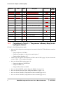
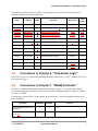
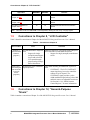
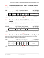
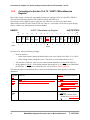
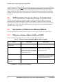
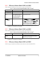
MC68VZ328UMAD/D
Rev. 7, 10/2001
MC68VZ328
Addendum to
MC68VZ328 Integrated Processor User’s
Manual (DragonBall™ VZ)
This addendum supplements, and should be used in conjunction with, the MC68VZ328 Integrated
Processor User’s Manual, rev. 0 (order number MC68VZ328UM/D). Section 1, “User’s Manual Errata,”
corrects information in the user’s manual, and Section 2, “Additional Information,” provides supplemental
information.
1
User’s Manual Errata
Table 1 identifies and corrects errata that appear in more than one location in the user’s manual.
Subsequent subsections identify and correct errata in specific chapters.
Table 1. Errata in Multiple Locations
Error Locations
Error
Figure 2-1 (page 2-2)
Table 2-1 (page 2-3)
Section 2.8 (page 2-7)
The mnemonic that is used for the
LCD Frame Marker signal—LFLM—is
incorrect.
Section 8.2 (page 8-3)
Section 8.2.1 (page 8-3)
Section 8.2.1.1 (page 8-3)
Figure 8-2 (page 8-4)
Table 10-14 (page 10-13)
Figure 19-13 (page 19-17)
Figure 19-14 (page 19-18)
Table 19-15 (page 19-18)
Specifications and information herein are subject to change without notice.
© Motorola, Inc., 2001. All rights reserved.
Corrections
The mnemonic for the LCD Frame
Marker signal is LFRM. Replace all
occurrences of LFLM with LFRM.
Corrections to Chapter 1, “Introduction”
Table 1. Errata in Multiple Locations (Continued)
Error Locations
Error
Corrections
Section 8.2.1 (page 8-3)
Table 8-12 (page 8-17)
The mnemonic that is used for the
LCD Frame Marker signal—FLM—is
incorrect.
The mnemonic for the LCD Frame
Marker signal is LFRM. Replace all
occurrences of FLM with LFRM.
Section 8.2.5 (page 8-9)
Section 8.2.5.1 (page 8-9)
Table 8-19 (page 8-21)
The mnemonic that is used for the
LCD Frame Marker signal—FRM—is
incorrect.
The mnemonic for the LCD Frame
Marker signal is LFRM. Replace all
occurrences of FRM with LFRM.
The mnemonic that is used for the
frame marker polarity bit—
FLMPOL—is incorrect.
The mnemonic for the frame marker
polarity bit is FRMPOL. Replace all
occurrences of FLMPOL with FRMPOL.
Section 8.2 (page 8-2)
Section 8.2.1 (page 8-3)
Section 8.2.5 (page 8-9)
Section 8.2.5.1 (page 8-9)
Table 8-12 (page 8-17)
Table 8-19 (page 8-21)
The mnemonic that is used for the
LCD Line Pulse signal—LP—is incorrect.
The mnemonic for the LCD Line Pulse
signal is LLP. Replace all occurrences of
LP with LLP.
Table 3-1 (page 3-5)
Table 3-2 (page 3-13)
Section 14.4.2 (page14-12)
The UBAUD1 reset value—0x003F—
is incorrect.
The reset value is 0x0002.
(See Section 1.2 and Section 1.8 of this
document)
Table 3-1 (page 3-6)
Table 3-2 (page 3-13)
Section 14.4.9 (page14-22)
The UBAUD2 reset value—0x003F—
is incorrect.
The reset value is 0x0002.
(See Section 1.2 and Section 1.8 of this
document)
Section 8.2.1.1 (page 8-3)
LPOLCF register (page 8-16)
Table 8-16 (page 8-16)
1.1
Corrections to Chapter 1, “Introduction”
Table 2 corrects errors in Chapter 1 of the MC68VZ328 Integrated Processor User’s Manual.
Table 2. Corrections to Chapter 1
2
Error Location
Error
Correction
Chapter 1,
“Introduction”
(page 1-1)
The third sentence of the second
paragraph reads as follows:
“Additionally, the new DragonBall
VZ integrates the logic needed to
support color LCD panels on-chip.”
Delete this sentence.
Section 1.1,
“Features of the
MC68VZ328”
(page 1-3)
Under the bullet for “Real-time
clock/sampling timer,” the first subbullet states: “Separate power supply for the RTC.”
Delete this sub-bullet.
MC68VZ328 Integrated Processor User’s Manual Addendum
Corrections to Chapter 3, “Memory Map”
Table 2. Corrections to Chapter 1 (Continued)
Error Location
Section 1.1,
“Features of the
MC68VZ328”
(page 1-3)
1.2
Error
Correction
Under the bullet for “LCD controller,” the first sub-bullet identifies
support for “color STN” panels.
The sub-bullet should read as follows:
•
LCD controller
— Software-programmable screen size to
support single (nonsplit) monochrome
panel (up to 640 × 512 pixels)
Corrections to Chapter 3, “Memory Map”
There are various corrections that apply to both Table 3-1 and Table 3-2. The same set of corrections applies
to each table, but the information is presented twice because the tables are arranged differently.
1.2.1
Corrections to Table 3.1, “Programmer’s Memory Map (Sorted
by Address)”
In Table 3-1, the following changes apply:
•
At the address 0xFFFFF10A (page 3-2):
— Change the Name to CSCTRL1.
— Change the Description to “Chip-select control register 1.”
— Change the Page Number to 6-17.
•
Create new table rows for the addresses 0xFFFFF10C and 0xFFFFF150 (page 3-2). See the
corrected version of Table 3-1 for complete information.
•
At the address 0xFFFFF902, change the Reset Value to 0x0002 (page 14-12).
•
At the address 0xFFFFF912, change the Reset Value to 0x0002 (page 14-12).
•
In the row for the LRRA register, which is listed at the address 0xFFFFFA29, make these
corrections (page 3-6):
— Change the Address to 0xFFFFFA28.
— Change the Width to 16.
— Change the Reset Value to 0x00FF.
•
At the address 0xFFFFFB0C, change the Width to 16 (page 3-7).
•
At the address 0xFFFFFB12, change the Width to 16 (page 3-7).
The following partial reproduction of Table 3-1 incorporates these corrections. New and corrected
information appears in red and is underlined.
Address
Name
Width
...
...
...
...
0xFFFFF10A
CSCTRL1
16
Chip-select control register 1
Description
User’s Manual Errata
Reset Value
Page
Number
...
...
0x0000
6-17
3
Corrections to Chapter 3, “Memory Map”
Address
Name
Width
0xFFFFF10C
CSCTRL2
16
Chip-select control register 2
...
...
...
...
0xFFFFF150
CSCTRL3
16
Chip-select control register 3
...
...
...
...
0xFFFFF902
UBAUD1
16
UART unit 1 baud control register
...
...
...
...
0xFFFFF912
UBAUD2
16
UART unit 2 baud control register
...
...
...
...
0xFFFFFA28
LRRA
16
LCD refresh rate adjustment register
...
...
...
...
0xFFFFFB0C
RTCCTL
16
RTC control register
...
...
...
...
0xFFFFFB12
STPWCH
16
Stopwatch minutes register
1.2.2
Description
Reset Value
Page
Number
0x1000
6-18
...
...
0x9C00
6-20
...
...
0x0002
14-12
...
...
0x0002
14-12
...
...
0x00FF
8-18
...
...
0x0080
11-10
...
...
0x003F
11-14
Corrections to Table 3.2, “Programmer’s Memory Map (Sorted
by Register Name)”
In Table 3-2, the following changes apply.
•
In the row for the chip-select control register, whose name is listed as CSCR, make these corrections
(page 3-8):
— Change the Name to CSCTRL1.
— Change the Description to “chip-select control register 1.”
— Change the Page Number to 6-17.
•
Add new rows for registers with the names CSCTRL2 and CSCTRL3 (page 3-8). See the corrected
version of Table 3-2 for complete information.
•
In the row for the LRRA register (page 3-9):
— Change the Address to 0xFFFFFA28.
— Change the Width to 16.
— Change the Reset Value to 0x00FF.
4
•
In the row for the RTCCTL register, change the Width to 16 (page 3-12).
•
In the row for the STPWCH register, change the Width to 16 (page 3-12).
•
In the row for the UBAUD1, change the Reset Value to 0x0002 (page 14-12).
•
In the row for the UBAUD2, change the Reset Value to 0x0002 (page 14-12).
MC68VZ328 Integrated Processor User’s Manual Addendum
Corrections to Chapter 6, “Chip-Select Logic”
The following version of portions of Table 3-2 incorporates these corrections. New and corrected
information appears in red and is underlined.
Reset Value
Page
Number
...
...
Chip-select control register 1
0x0000
6-17
16
Chip-select control register 2
0x1000
6-18
0xFFFFF150
16
Chip-select control register 3
0x9C00
6-20
...
...
...
...
...
...
LRRA
0xFFFFFA28
16
LCD refresh rate adjustment register
0x00FF
8-18
...
...
...
...
16
RTC control register
0x0080
11-10
...
...
...
...
0x003F
11-14
...
...
Name
Address
Width
...
...
...
...
CSCTRL1
0xFFFFF10A
16
CSCTRL2
0xFFFFF10C
CSCTRL3
...
RTCCTL
0xFFFFFB0C
...
Description
STPWCH
0xFFFFFB12
16
Stopwatch minutes register
...
...
...
...
UBAUD1
0xFFFFF902
16
UART unit 1 baud control register
0x0002
14-12
UBAUD2
0xFFFFF912
16
UART unit 2 baud control register
0x0002
14-12
1.3
Corrections to Chapter 6, “Chip-Select Logic”
In Section 6.1 (page 6-1), in the fourth paragraph, the third sentence refers to “CDL.” Change CDL to CSL
(for “chip-select logic”).
1.4
Corrections to Chapter 7, “DRAM Controller”
In Table 7-9, “SDRAM Bank Address Programming Examples” (page 7-17), the unit for the memory
values in the Application column is incorrect. In the second row through the fifth row, change all instances
of “Mbyte” to “Mbit.”
The following version of Table 7-9 incorporates these corrections. Corrected information appears in red
and is underlined.
Application
BNKADDH
BNKADDL
Make all SDRAM appear as one
single bank
11
11
None
Two banks of SDRAM—for example, 16 Mbit
00
11
Choose PA20 as bank selection address
Remarks
User’s Manual Errata
5
Corrections to Chapter 8, “LCD Controller”
Application
BNKADDH
BNKADDL
Four banks of SDRAM—for
example, 64 Mbit
01
10
Choose PA22 and PA21 as bank selection
address
Four banks of SDRAM—for
example, 128 Mbit
01
10
Choose PA22 and PA23 as bank selection
address
Four banks of SDRAM—for
example, 256 Mbit
10
10
Choose PA24 and PA23 as bank selection
address
Note:
1.5
Remarks
These bits are all set in EDO RAM or Fast Page Mode, allowing the use of only one page register.
Corrections to Chapter 8, “LCD Controller”
Table 3 identifies corrections to Chapter 8 of the MC68VZ328 Integrated Processor User’s Manual.
Table 3. Corrections to Chapter 8
Error Location
Error
Section 8.1,
“LCD Controller
Features”
(page 8-1)
The third bullet refers to support for
color:
Section 8.2.1,
“Connecting the
LCD Controller
to an LCD
Panel”
(page 8-3)
No description of the CONTRAST
signal is provided.
1.6
•
Support for single
(nonsplit) monochrome
screen and color STN
LCD panels through
preprocessing of image
data with software
Correction
Delete the reference to color panels and all subsequent
text in this bullet. The third bullet should read:
•
Support for single (nonsplit) monochrome
screen
Add a bullet describing the CONTRAST signal as follows:
•
CONTRAST—The LCD CONTRAST
output signal may be used to control the
contrast of an LCD panel. The
CONTRAST signal provides a pulsewidth-modulated signal whose pulse width
and clock source are adjustable in software.
See Section 8.3.18, “PWM Contrast
Control Register,” for more information.
Corrections to Chapter 12, “General-Purpose
Timers”
Table 4 contains a correction to Chapter 12 of the MC68VZ328 Integrated Processor User’s Manual.
6
MC68VZ328 Integrated Processor User’s Manual Addendum
Corrections to Chapter 13, “Serial Peripheral Interface 1 and 2”
Table 4. Correction to Chapter 12
Error Location
Error
Correction
Table 12-2
(page 12-7)
In the row for bit 4, the IRQEN (interrupt
request enable) bit, the Setting column presents the bit as a 2-bit field.
Change the listed setting options from 2-bit
values to 1-bit values, as follows:
0 = Disable the compare interrupt (default).
1 = Enable the compare interrupt.
1.7
Corrections to Chapter 13, “Serial Peripheral
Interface 1 and 2”
This section contains corrections to Chapter 13 of the MC68VZ328 Integrated Processor User’s Manual.
1.7.1
Corrections to Section 13.3.1, “SPI 1 Receive Data Register”
The SPI 1 receive data register is presented as an 8-bit register, which is incorrect. It is a 16-bit register.
On page 13-4, replace the SPIRXD register display with the following one:
SPIRXD
SPI 1 Receive Data Register
BIT 15
14
13
12
11
10
9
8
0x(FF)FFF700
7
6
5
4
3
2
1
BIT 0
DATA
TYPE
r
r
r
r
r
r
r
r
r
r
r
r
r
r
r
r
0
0
0
0
0
0
0
0
0
0
0
0
0
0
0
0
RESET
0x0000
In addition, in the Name column of Table 13-1, replace the identifier “Bits 7–0” with “Bits 15–0.”
1.7.2
Corrections to Section 13.3.2, “SPI 1 Transmit Data Register”
The SPI 1 transmit data register is presented as an 8-bit register with a reset value of 0x00, which is
incorrect. It is a 16-bit register with a reset value of 0x0000.
On page 13-5, replace the SPITXD register display with the following one:
SPITXD
SPI 1 Transmit Data Register
BIT 15
14
13
12
11
10
9
8
0x(FF)FFF702
7
6
5
4
3
2
1
BIT 0
DATA
TYPE
w
w
w
w
w
w
w
w
w
w
w
w
w
w
w
w
0
0
0
0
0
0
0
0
0
0
0
0
0
0
0
0
RESET
0x0000
In addition, in the Name column of Table 13-2, replace the identifier “Bits 7–0” with “Bits 15–0.”
User’s Manual Errata
7
Corrections to Chapter 14, “Universal Asynchronous Receiver/Transmitter 1 and 2”
1.8
Corrections to Chapter 14, “Universal
Asynchronous Receiver/Transmitter 1 and 2”
This section contains corrections to Chapter 14 of the MC68VZ328 Integrated Processor User’s Manual.
Table 5 presents a correction to Section 14.1, “Introduction to the UARTs.”
Table 5. Correction to Section 14.1
Errata
Location
Error
Section 14.1,
“Introduction to
the UARTs”
(page 14-2)
1.8.1
Corrections
In the second bulleted list of features,
which is introduced by the statement “The
UART 2 module is an enhanced version of
the UART 1,” an additional feature is missing.
Add the following bullet to the end of the list:
•
The non-integer prescaler value can
be programmed to be 1, which
provides the maximum nonstandard
baud rate of 2.07 MHz with the 16x
sample clock.
Corrections to Table 14.1, “Non-Integer Prescaler Values”
Table 14-1’s final row, for the select field value of 111, erroneously omits information (page 14-8).
Corrections to this row are as follows:
•
The Minimum Divisor value is 1 (UART 2 only).
•
The Maximum Divisor value is 1 (UART 2 only).
The following table excerpt displays the corrected information, which appears in red and is underlined.
1.8.2
Select (Binary)
Minimum Divisor
Maximum Divisor
Step Size
111
1 (UART 2 only)
1 (UART 2 only)
—
Corrections to Section 14.4.2, “UART 1 Baud Control
Register”
In the Reset row of the register display the correct reset value is 0x0002. A corrected version of the register
display follows, with the new information in red and underlined.
UBAUD1
UART 1 Baud Control Register
BIT 15
14
TYPE
RESET
8
0
0
13
12
11
10
9
8
UCL
KDI
R
BAU
D
SRC
rw
rw
rw
rw
rw
0
0
0
0
0
0
7
6
0x(FF)FFF902
5
4
DIVIDE
3
2
1
BIT 0
PRESCALER
0
0
rw
rw
rw
rw
rw
rw
1
1
1
1
1
1
0x0002
MC68VZ328 Integrated Processor User’s Manual Addendum
Corrections to Chapter 14, “Universal Asynchronous Receiver/Transmitter 1 and 2”
1.8.3
Corrections to Section 14.4.4, “UART 1 Transmitter Register”
In the Type row of the register display bits 10 and 9 are read-only. A corrected version of the register
display follows, with the new information in red and underlined.
UTX1
UART 1 Transmitter Register
BIT 15
14
13
12
11
10
9
8
FIFO
EMPTY
FIFO
HALF
TX
AVAI
L
SEND
BREAK
NO
CTS1
BUSY
CTS1
STAT
CTS1
DELTA
r
r
r
rw
rw
r
r
rw
w
w
w
w
w
0
0
0
0
0
0
0
0
0
0
0
0
0
TYPE
RESET
1.8.4
0x(FF)FFF906
7
6
5
4
3
1
BIT
0
w
w
w
0
0
0
2
TX DATA
0x0000
Corrections to Section 14.4.9, “UART 2 Baud Control
Register”
In the Reset row of the register display the correct reset value is 0x0002. A corrected version of the register
display follows, with the new information in red and underlined.
UBAUD2
UART 2 Baud Control Register
BIT 15
14
13
TYPE
RESET
1.8.5
0
0
12
11
10
UCLK
DIR
BAUD
SRC
rw
rw
rw
0
0
0
0
9
8
7
6
0x(FF)FFF912
5
4
DIVIDE
3
2
1
BIT 0
PRESCALER
rw
rw
0
0
0
0
rw
rw
rw
rw
rw
rw
1
1
1
1
1
1
0x0002
Corrections to Section 14.4.11, “UART 2 Transmitter Register”
In the Type row of the register display bits 10 and 9 are read-only. A corrected version of the register
display follows, with the new information in red and underlined.
UTX2
TYPE
RESET
UART 2 Transmitter Register
BIT 15
14
13
12
11
10
9
8
FIFO
EMPTY
FIFO
HALF
TX
AVAIL
SEND
BREAK
NO
CTS2
B
U
S
Y
CTS2
STAT
CTS2
DELTA
0x(FF)FFF916
7
6
5
4
3
2
1
BIT 0
TX DATA
r
r
r
rw
rw
r
r
rw
w
w
w
w
w
w
w
w
0
0
0
0
0
0
0
0
0
0
0
0
0
0
0
0
0x0000
User’s Manual Errata
9
Corrections to Chapter 14, “Universal Asynchronous Receiver/Transmitter 1 and 2”
1.8.6
Corrections to Section 14.4.12, “UART 2 Miscellaneous
Register”
Bit 8 of this register is incorrectly represented as being reserved (page 14-26). It is the RTS2 TRIG bit.
This correction affects the display of the UMISC2 register and Table 14-14.
In the display of the UMISC2 register, ignore the grey fill for bit 8. In the cell for the bit name
abbreviation, insert RTS2 TRIG. In the TYPE row, insert rw. A corrected version of the register display
follows, with the new information in red and underlined.
UMISC2
TYPE
RESET
UART 2 Miscellaneous Register
BIT
15
14
13
12
11
10
BAU
D
TES
T
CLK
SR
C
FOR
CE
PERR
LO
OP
BAU
D
RESE
T
IR
TES
T
rw
rw
rw
rw
rw
rw
0
0
0
0
0
0
9
0
0x(FF)FFF918
8
7
6
5
4
3
2
RTS2
TRIG
RTS2
CONT
RT
S2
IR
DA
EN
IRD
A
LO
OP
RX
PO
L
TX
PO
L
rw
rw
rw
rw
rw
rw
rw
0
0
0
0
0
0
0
1
BIT
0
0
0
0x0000
In Table 14-14, make the following changes:
•
In the seventh row,
— In the Name column, change the identification of the reserved bits from “Bits 9–8” to “Bit 9.”
— In the Setting column, change the text to “This bit is reserved and should be set to 0.”
•
Just after the seventh row, insert a new row that contains information for the RTS2 TRIG bit.
•
In the eighth row for bit 7, in the Setting column, change the text to “0 = RTS2 pin is controlled by
the RTS2 bit. 1 = RTS2 pin is controlled by the receiver FIFO and RTS2 TRIG bit.”
The following table excerpt displays the new and corrected information, which appears in red and is
underlined.
Reserved
Bit 9
Reserved
This bit is reserved and should be
set to 0.
RTS2
TRIG
Bit 8
RTS2 Trigger Source Select—This bit selects the control of
the RTS2 pin when the RTS2 CONT bit (bit 7) is 1.
0 = RTS2 pin is asserted when the
number of filled slots is equal
to RxFIFO level marker.
1 = RTS2 pin is asserted when only
one slot is available in the
receiver FIFO.
RTS2
CONT
Bit 7
RTS2 Control—This bit selects the function of the RTS2 pin.
0 = RTS2 pin is controlled by the
RTS2 bit.
1 = RTS2 pin is controlled by the
receiver FIFO and RTS2 TRIG
bit.
10
MC68VZ328 Integrated Processor User’s Manual Addendum
Corrections to Chapter 20, “Mechanical Data and Ordering Information”
1.8.7
Corrections to Table 14-15, “UART 2 Non-Integer Prescaler
Register Description”
For the select field (bits 10–8), Table 14-15 incorrectly presents the Setting for the option 111 as “Disable
the non-integer prescaler” (page 14-28). The correct Setting for this option is “Divide value is 1.”
The following table excerpt displays the correct information, which appears in red and is underlined.
Name
SELECT
Bits 10–8
1.9
Description
Setting
Tap Selection—This field selects a tap from
the non-integer divider.
000 = Divide range is 2 to 3 127/128 in 1/128 steps.
001 = Divide range is 4 to 7 63/64 in 1/64 steps.
010 = Divide range is 8 to 15 31/32 in 1/32 steps.
011 = Divide range is 16 to 31 15/16 in 1/16 steps.
100 = Divide range is 32 to 63 7/8 in 1/8 steps.
101 = Divide range is 64 to 127 3/4 in 1/4 steps.
110 = Divide range is 128 to 255 1/2 in 1/2 steps.
111 = Divide value is 1.
Corrections to Chapter 20, “Mechanical Data and
Ordering Information”
Table 6 corrects information in Figure 20-1.
Table 6. Correction to Figure 20-1
Error Location
Figure 20-1, “MC68VZ328 TQFP Pin
Assignments—Top View” (page 20-2)
2
Error
Pin 73 is labeled as VSS.
Correction
Pin 73 should be labeled as NC.
Additional Information
This section provides information that is not included in the MC68VZ328 Integrated Processor User’s
Manual or that supplements information in the manual.
2.1
System Power-up Time and HIZ Pin Design
Consideration
The MC68VZ328 enters 68K test mode if the HIZ pin is toggled once when the reset signal is still asserted.
In this mode, many MC68VZ328 signals become 68K core signals, and the default reset states of the I/O
pins are overridden. Some pins could oscillate due to the 68K core running with the 32 kHz clock provided
through the normal oscillator circuit input. To switch the MC68VZ328 back to normal mode, apply a
normal reset with the HIZ pin staying high after the power up. Due to this consideration, take special care
in designing the HIZ pin connection.
Additional Information
11
VCO Operation Frequency Range Consideration
Another situation can produce the same result. If the system power-up sequence has a long intermediate
voltage level below 1.8 V, the HIZ pin may have undetermined and toggling states when its voltage level is
increased slowly with the power source due to internal pull-up resistors. This situation may wrongly
instruct the MC68VZ328 to enter 68K test mode. The I/O pins will then become 68K core signals and
oscillate. Unexpected noise may be generated before a valid reset is re-asserted after the system is fully
powered up.
2.2
VCO Operation Frequency Range Consideration
The PLL design allows the VCO operation frequency range of 50 MHz to 80 MHz. For best PLL
performance, the recommended range of operation is at 60 MHz to 70 MHz. Therefore, setting the
nominal/default frequency at 66 MHz already covers the allowable drift introduced by process variation.
Any change to PC or QC values in PLLFSR for other VCO frequencies is not recommended and may
cause PLL stability issues or jitter.
2.3
Summaries of Differences Between Masks
The following subsections identify differences between various pairs of masks of the MC68VZ328.
2.3.1
Differences Between Masks 0K85C and 2K85C
Table 7 summarizes the differences between these two masks of the MC68VZ328.
Table 7. Differences Between MC68VZ328 Masks 0K85C and 2K85C1
Feature
Reset value of ID register
(0xFFFFF004)
ICEM control bits
Mask 0K85C
Mask 2K85C
0x5601
0x5600
The ICEM control bits have a short
circuit problem (see the MC68VZ328
Chip Errata document). The SWEN
bit in the ICE module control register
(0xFFFFFD0C) is bit 5.
The problem is fixed. The SWEN bit in
the ICE module control register
(0xFFFFFD0C) is bit 6.
DTACK pin output function
The DTACK pin output function is fixed.
The DTACK can be programmed to output by setting bit 0 of the Port G direction register (0xFFFFF430) to 1.
Schmitt trigger hythesis of the
RESET pin
The hythesis is enhanced.
1.
12
With regard to variations between masks, some information in the MC68VZ328 Integrated Processor User’s Manual, rev. 0, is specific only to mask 2K85C.
MC68VZ328 Integrated Processor User’s Manual Addendum
Summaries of Differences Between Masks
2.3.2
Differences Between Masks 2K85C and 3K85C
Table 8 summarizes the differences between these two masks of the MC68VZ328.
Table 8. Differences Between MC68VZ328 Masks 2K85C and 3K85C1
Feature
Mask 2K85C
Mask 3K85C
Reset value of ID register (0xFFFFF004)
0x5600
0x5601
SPI 1
There are problems with reading
SPI 1 RXFIFO and writing to
SPI 1 TXFIFO during data
exchanges (see the MC68VZ328
Chip Errata document).
EMUCS function on
PG4/EMUCS pin
1.
2.3.3
These problems are fixed.
The EMUCS function on the PG4/EMUCS pin is
replaced by CSC0. The PB2/CSC0/RAS0 pin remains
unchanged. It provides one more opening for CSC0.
The CSC0 can function on the PG4/EMUCS pin even
when the DRAM bit in chip-select register D is set.
The memory map and function of CSC0 are still controlled by the registers related to chip-select C.
With regard to variations between masks, some information in the MC68VZ328 Integrated Processor User’s Manual, rev. 0, is specific only to mask 2K85C.
Differences Between Masks 3K85C and 4K85C
Table 9 summarizes the differences between these two masks of the MC68VZ328.
Table 9. Differences Between MC68VZ328 Masks 3K85C and 4K85C1
Feature
Wafer fabrication
process
1.
2.3.4
Mask 3K85C
Mask 4K85C
The wafer fabrication process has been changed to
standardize the trench etch thickness in MOS 13.
No product function is affected.
With regard to variations between masks, some information in the MC68VZ328 Integrated Processor User’s Manual, rev. 0, is specific only to mask 2K85C.
Differences Between Masks 4K85C and 5K85C
Table 10 on page 14 summarizes the differences between these two masks of the MC68VZ328.
Additional Information
13
Table 10. Differences Between MC68VZ328 Masks 4K85C and 5K85C1
Feature
Mask 4K85C
Mask 5K85C
Reset value of ID register (0xFFFFF004)
0x5601
0x5700
SPI 1
SPI 1 transmits a wrong bit if a write
occurs to SP1 TXFIFO during data
exchanges (see the MC68VZ328 Chip
Errata document).
P/D function on PG3/
HIZ/P/D pin
1.
2.
2.4
This problem is fixed.
The P/D function on the PG3/HIZ/P/D pin is
replaced by CSB1.2
With regard to variations between masks, some information in the MC68VZ328 Integrated Processor User’s Manual, rev. 0, is specific only to mask 2K85C.
To enable the CSB1 function, the Port G direction register’s bit 3 should be set to 1, and the Port G select
register’s bit 3 should be set to 0.
External Pin Pull-down Consideration
When connecting an external pull-down resistor, users are cautioned to use a resistor with a maximum
value of 15 kohm. This value ensures that a logic low level appears to the internal detection circuit.
Motorola reserves the right to make changes without further notice to any products herein. Motorola makes no warranty,
representation or guarantee regarding the suitability of its products for any particular purpose, nor does Motorola assume any
liability arising out of the application or use of any product or circuit, and specifically disclaims any and all liability, including without
limitation consequential or incidental damages. “Typical” parameters which may be provided in Motorola data sheets and/or
specifications can and do vary in different applications and actual performance may vary over time. All operating parameters,
including “Typicals” must be validated for each customer application by customer’s technical experts. Motorola does not convey
any license under its patent rights nor the rights of others. Motorola products are not designed, intended, or authorized for use as
components in systems intended for surgical implant into the body, or other applications intended to support life, or for any other
application in which the failure of the Motorola product could create a situation where personal injury or death may occur. Should
Buyer purchase or use Motorola products for any such unintended or unauthorized application, Buyer shall indemnify and hold
Motorola and its officers, employees, subsidiaries, affiliates, and distributors harmless against all claims, costs, damages, and
expenses, and reasonable attorney fees arising out of, directly or indirectly, any claim of personal injury or death associated with
such unintended or unauthorized use, even if such claim alleges that Motorola was negligent regarding the design or manufacture
of the part. Motorola, Inc. is an Equal Opportunity/Affirmative Action Employer. Motorola, the stylized
and all other trademarks
indicated as such herein are registered trademarks of Motorola, Inc. ® Registered U.S. Pat. and Tm. Office. All other tradenames,
trademarks, and registered trademarks are the property of their respective owners.
How to reach us:
USA/EUROPE/Locations Not Listed: Motorola Literature Distribution; P.O. Box 5405, Denver, Colorado, 80217.
1–303–675–2140 or 1–800–441–2447
JAPAN: Motorola Japan Ltd.; SPS, Technical Information Center, 3–20–1, Minami–Azabu, Minato–ku,
Tokyo 106–8573 Japan. 81–3–3440–3569
ASIA/PACIFIC: Motorola Semiconductors H.K. Ltd., Silicon Harbour Centre, 2 Dai King Street,
Tai Po Industrial Estate, Tai Po, N.T., Hong Kong. 852–26668334
Technical Information Center: 1–800–521–6274
HOME PAGE: http://www.motorola.com/semiconductors/
MC68VZ328UMAD/D