1
US006311267B1
(12)
(54)
(75)
United States Patent
(10) Patent N0.:
Nguyen et al.
(45) Date of Patent:
US 6,311,267 B1
Oct. 30, 2001
JUST-IN-TIME REGISTER RENAMING
5,708,841
1/1998 Popescu et al. ..................... .. 712/23
TECHNIQUE
5,758,117 *
5,872,950 *
5/1998 Patel et al. ......................... .. 712/217
2/1999 Levitan et al.
. 712/217
Inventors:
Dung Quoc Nguyen; Hung Qui Le,
5,872,985 :
2/1999
both of Austin, TX (Us)
5,944,812
8/1999 Walker ................................. .. 712/23
_
_
_
_
_
(*) Notice:
_
. . . . .. 712/1
* cited by examiner
(73) Ass1gnee: International Business Machines
Corporation, Afmonk, NY (Us)
_
Kimura . . . . . . . .
Primary Examiner—Eddie Chan
_
_
Assistant Examiner—Gautam R. Patel
Sub]ect'to any d1scla1mer,the term of this
(74) Attorney) Agent) 0,, Firm_AnthOny V_ 3 England;
patent is extended or adJusted under 35
Casimer K salys
U.S.C. 154(b) by 0 days.
(57)
(21)
(22)
Appl' NO‘: 09/196’908
Filed;
Nov, 20, 1998
7
(51)
Int. Cl.
(52)
US. Cl. ........................................... .. 712/217; 712/219
(58)
Field of Search
A target register of an instruction is assigned a rename
register in response to the instruction being issued. That is,
the target register is renamed at issue time, not at dispatch
...................................................... .. G06F 9/38
.
-
.
-
.
.
-
-
-
-
-
-
-
the present invention, includes logic for allocating and
.
.
deallocatmg tWo sets of rename registers, one set from a
References Cited
regular rename buffer and another set from an over?ow
rename buffer. According to this allocation/deallocation
U'S' PATENT DOCUMENTS
logic, if the oldest dispatched, noncompleted instruction is
4,992,938
5,497,499
576257837 *
5,630,149
-
rename register allocation/deallocation logic, according to
................................... .. 712/216, 217,
712/218, 219, 228, 23
5,673,427
5,699,538
.
time. To handle a neW deadlock issue this gives rise to,
_
(56)
ABSTRACT
2/1991 Cooke et al. ....................... .. 712/217
3/1996 Garg et al
-- 712/217
4/1997 Popescu et a1‘
712/23
5/1997
Bluhm .......... ..
ready for assignment of a rename register and the regular
rename buffer is full, then a rename register is assigned from
the over?ow rename buffer to this instruction.
712/217
9/1997 Brown et al.
712/245
12/1997 Le et a1. ............................... .. 712/23
11 Claims, 12 Drawing Sheets
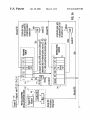
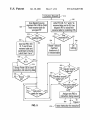
Instruction Dispatch
510
K 550
520 /
Use dispatch source
registers RA & RB to CAM
read rename table for
youngest RT
write RT, IID, R, Y and V to
rename table and t0 IQ. Use
dispatch RT to search the
rename table for matching RTs
556
read out RID, IID,
R, Y and V from
rename table and
send them to the IQ.
Latch them "as is".
/
NO
Reset Y bits at
D0
matched
nothing
locations to 0
in rename table
Snoop Finish IID to see it
execution unit returning data
butter full?
NO
.
,
is
instruction oldest
In machine?
YES
Assign new RID to
instruction being issued.
/
566
,_, To
Figure6
570. A Issue instruction for execution I
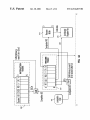
U.S. Patent
0a. 30, 2001
Sheet 5 0f 12
US 6,311,267 B1
_
_
O
<iv
cQ:/053|1o8_ ">mDE2EoN_92235Emega;
_|I“S0:2501
6E<<
2856%1;,‘
“
59:1_E5
_E|Cg2\3;J8
23
/1,2m
m:2?25E283_Q5 .25 E25O292 2
m
n
z
_
o>m9m
0 5_2:5239
gas
a
95
7
m_5m5o
5_2 8352m
i{|l! 5%
F_
n
2
_
$26
52%
|.<1
U.S. Patent
0a. 30, 2001
Sheet 7 of 12
US 6,311,267 B1
Instruction Dispatch _/— 51o
+
£
+
Use dispatch source
write RT, IID, R, Y and V to
f registers RA & RB to CAM
520
read rename table for
rename table and to IQ. Use
dispatch RT to search the
youngest RT
rename table for matching RTs
525
552
YES
Y
YES
Any
matched HTS
53° \ F
read out RID, no,
554
NO
\
556
_
/
rename table and
send them to the IQ.
matched
_|°Cat'°n$ to 0
Latch them "as is".
t
532 \
in rename table
nothing
YES "
v
/ 534
A
560
Snoop Finish IID to see if
-
NO
matched RTs
,
NO
f 550
-
IS
YES
-
NO
regular rename
execution unrt returning data
buffer fun?
562
IS
\/
W0
buffer
V
1*
1
‘
NO
564
is
' truction
ins
oldest
\ in machine?
YES
‘I
Assign new RID to
‘
instruction being issued.
"
FIG. 5
/
To
566
Figure 6
570 / Issue instruction for execution
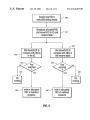
U.S. Patent
0a. 30, 2001
Sheet 8 0f 12
Assign new RID to
instruction being issued.
US 6,311,267 B1
f 566
i
Broadcast allocated-RID
and issued-IID to IQ and
rename table.
t
620 /
t
i
Use issued-IID to
compare with DIIDs
in the IQ.
f 640
Use issued-IID to
compare with IIDs in
the rename table
645
Any
matched
'2
'
650
r /
Do
nothing
635 f write in allocated-
660 I write in allocated
RID at matched
locations
RID at matched
locations
FIG. 6
U.S. Patent
0a. 30, 2001
Sheet 9 0f 12
US 6,311,267 B1
Execution Engine
V
FIG. 7
Broadcast Finish IID to
IQ and rename table.
i
i
730 /
‘I
Use FinishIID to
compare with DIIDs
in the IQ.
735
Use Finish IID to
compare with IIDs in
the rename table
75
NO .Y
—
matched
?
740
/ 750
YES
5
Any
matched
?
YES
758
i /
v/
Do
Do
nothing
745 f
nothing
891 R
i0 1
at matched
locations
760 f
Set Fi bit to t
at matched
locations
U.S. Patent
0a. 30, 2001
Sheet 10 0f 12
Completion Logic
US 6,311,267 B1
/ 810
e. g. check for interrupt
820
I
position resolving spec exe
FIG. 8
Broadcast Completion IID to IQ, rename
table, and RID allocation/de-allocation logic / e25
l
830
\
l
l
f 850
Use Compm?on IID to
Use Com letion IID to
compare with DIIDs in the IQ.
comparepwirh {IDS in
rename table
835
NO
Any
83\8 i_
'
o
l
Do
'
Set V bit to O at matched
nothing
location. Also read out RID
at same location and send it
_
840 f
f 855
to RID allocation/de
Set V bit to 0
allocation logic. FllD is also
at matched
send to rename butter. RT
location-
is also read out.
858 \
l
}
De-allocate completed RID
and release the RID to
Use RID as read address to
lead out Completed data
rename allocation logic to
from 1h? rename buffer and
be re-used by younger
instruction,
K 860
send rtlto the architected
register file. Use RT as write
address to write in
completed data into the
architected register file
US 6,311,267 B1
1
2
J UST-IN-TIME REGISTER RENAMING
by the execution engines, and avoiding a rename buffer
being held for a long time by an instruction that is not ready
TECHNIQUE
to be executed. Consequently, more rename registers are
TECHNICAL FIELD
freed for younger instructions to be dispatched and
executed. But deadlock is avoided, because rename registers
This invention relates generally to data processing sys
are not permitted to be assigned to younger instructions to an
extent that younger instructions consume all available
tems and more speci?cally applies to recovery mechanisms
for such systems, particularly Where the system includes a
processor that is superscalar or has a pipelined execution
unit.
rename registers.
BRIEF DESCRIPTION OF THE DRAWINGS
BACKGROUND OF THE INVENTION
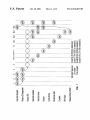
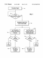
FIG. 1 is a timing diagram for a load miss causing delay
in execution of another nondependent instruction because
Currently, register renaming techniques employ a mecha
nism Where the target register of an instruction is assigned
a temporary rename buffer during the instruction dispatch
cycle of that instruction. This instruction Will hang on to the
temporary buffer from the dispatch time until it is completed
the load instruction locks up the rename buffer While a
nondependent add cannot be dispatched because the tem
15 porary rename buffer is full.
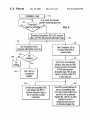
FIG. 2 is a timing diagram for just-in-time register renam
ing.
by the machine; Which locks up rename resources for a long
time (i.e. if the instruction is a load that misses L1 or L2
caches). A load miss in a cache is a typical event, for
example, Which looks up rename resources for a long time.
Thus, a need exists for improved renaming.
SUMMARY OF THE INVENTION
The foregoing need is addressed by the present invention,
25
as folloWs.
A target register of an instruction is assigned a rename
register in response to the instruction being issued. That is,
the target register is renamed at issue time, not at dispatch
associated With
associated With
associated With
DETAILED DESCRIPTION OF THE
PREFERRED EMBODIMENT
art each instruction needing a rename register is assigned a
35
art it is not possible for a deadlock to occur Wherein younger
instructions consume all available rename registers, and an
A sequence of instructions Will ?rst be shoWn, in FIG’s 1
and 2, to illustrate certain timing aspects of the embodiment.
FIG. 1. shoWs a dispatched add2 instruction Which causes
the rename buffer to be full upon assignment of rename
older instruction is unable to be dispatched for lack of a
identi?er for the I3 instruction, add2, at time 4. The add2
depends on completion of instruction II, the load
instruction, for one of the add2 operands, so the add2
instruction is stalled until time N+3. This, in turn, blocks the
dispatch of the add3 instruction until time N+4, When the
rename register. HoWever, according to the present
invention, instructions are dispatched in program order, but
are not assigned a rename register until issue time.
Furthermore, issuance depends on availability of source
operands, and completion is in program order. Therefore,
load instruction is completed and the rename resource has
one aspect of the present invention involves a recognition
45
deallocation resources it Would be possible for a deadlock to
occur. That is, if younger instructions Were issued before
older instructions to the extent of consuming all rename
been released. Note that instruction I4, the add3 instruction,
is not dependent on I1, I2, or I3, but because of the
dependency of I3 on I1, and the use of the last available
rename identi?er by the I3 instruction, I4 dispatch is delayed
until I1 completion, etc.
registers, this Would prevent issuance of an older instruction
for lack of a rename register. If an instruction cannot be
FIG. 2 shoWs the same code sequence as shoWn in FIG.
1. According to the present exemplary embodiment, the
target registers of the II through I3 instructions, load, addl,
issued, it cannot complete. Therefore, completion in pro
gram order Would be impossible if an oldest instruction
could not be issued for lack of a rename register. To avoid
this potential deadlock, rename register allocation/
deallocation logic, according to the present invention,
includes logic for allocating and deallocating tWo sets of
associated With
FIG. 9 is a block diagram of a system for the embodiment.
FIG. 10 is a block diagram of a CPU for the embodiment.
instructions are dispatched in program order, and in the prior
that Without adequate rename register and allocation/
execution.
completion of instructions.
time.
A neW deadlock issue arises due to the present invention
because of a potential race among instructions. That is,
rename register at dispatch; therefore, according to the prior
FIG. 3 shoWs data How at dispatch and
FIG. 4 shoWs data How at completion.
FIG. 5 is a How chart for logic steps
dispatching and issuance of instructions.
FIG. 6 is a How chart for logic steps
issuance of instructions.
FIG. 7 is a How chart for logic steps
execution of instructions.
FIG. 8 is a How chart for logic steps
and add2, are not assigned any rename registers during
dispatch. Consequently, the I4 instruction, add3, is noW
55
alloWed to execute much earlier, since the rename buffer is
not full When the add3 is dispatched. When the add3 is
dispatched, its operands are checked for availability. Since
add3 is not dependent on any instruction (i.e. all its operands
rename registers, one set from a regular rename buffer and
another set from an over?oW rename buffer. According to
this allocation/deallocation logic, an oldest instruction cur
are available), it is selected to be issued in cycle 5. At this
rently being processed in the processor is identi?ed as an
instruction Which is next to be completed. If this oldest
instruction is still in the instruction queue and the regular
rename buffer is full, then a rename register is assigned from
time (i.e. issue cycle), the target register of add3 is renamed
(i.e. rename ID assignment). Add3 is then executed in cycle
the rename over?oW buffer to this instruction, so the instruc
tion can execute.
Advantages of the present invention include alloWing the
rename buffer to remain free until it is ready to be consumed
65
6. In cycle 6, load operands are also available. In cycle 7 the
load instruction is selected to be issued, and its target register
is then renamed. Instruction I2 (Which depends on the load
instruction) is not renamed until cycle N+3.
In summary, add3 is alloWed to execute much earlier than
the load instruction, as compared to the normal rename cases
US 6,311,267 B1
3
4
shown in FIG. 1. That is, for the example of FIG. 2,
according to the present embodiment, the rename buffer
storage location, including RAM 914 or disk 920, 6)
attempting to access storage, including RAM 914 or disk
920, With an invalid effective address alignment, or 7) a
System Reset or Machine Check signal from a device (not
shoWn) directly connected to the processor 910 or another
device in the system 900 connected to the processor 910 via
the bus 912. These conditions are discussed further in the
remains un?lled. This is in contrast to the example of
opposed FIG. 1, Where the rename buffer is full in cycle 5
after instruction add2 is dispatched, and the rename buffer
being full blocks add3 from being dispatched.
Next, certain structural and functional aspects of a data
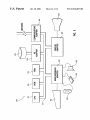
processing system for the embodiment Will be introduced.
above references, “The PoWerPC Architecture: A Speci?ca
Referring to FIG. 9, an example is shoWn of a data process
ing system 900 Which may be used for the invention. The
system has a central processing unit (CPU) 910, such as a
tion for a NeW Family of RISC Processors”, and “PoWerPC
604 RISC Microprocessor User’s Manual”.
Next, certain structural and functional aspects of a pro
cessor for the embodiment Will be introduced. Asuperscalar
10
PoWerPC microprocessor (“PoWerPC” is a trademark of
IBM Corporation) according to “The PoWerPC Architecture:
A Speci?cation for a NeW Family of RISC Processors”, 2d
edition, 1994, Cathy May, et al. Ed., Which is hereby
incorporated herein by reference. A more speci?c imple
15
processor has multiple elements Which operate in parallel to
process multiple instructions in a single processing cycle.
Pipelining involves processing instructions in stages, so that
the pipelined stages may process a number of instructions
mentation of a PoWerPC microprocessor is described in the
concurrently.
“PoWerPC 604 RISC Microprocessor User’s Manual”,
In a ?rst stage, referred to as an “instruction fetch” stage,
an instruction is fetched from memory. Then, in a “decode”
1994, IBM Corporation, Which is hereby incorporated herein
by reference. The allocation logic 320, rename table 310 and
rename buffer 414 (not shoWn) of the present invention are
included in CPU 910. The CPU 910 is coupled to various
other components by system bus 912. Read only memory
(“ROM”) 916 is coupled to the system bus 912 and includes
a basic input/output system (“BIOS”) that controls certain
basic functions of the data processing system 900. Random
access memory (“RAM”) 914, I/O adapter 918, and com
munications adapter 934 are also coupled to the system bus
912. I/O adapter 918 may be a small computer system
interface (“SCSI”) adapter that communicates With a disk
storage device 920. Communications adapter 934 intercon
stage, the instruction is decoded into different control bits,
Which in general designate i) a type of functional unit for
performing the operation speci?ed by the instruction, ii)
source operands for the operation and iii) destinations for
results of operations. Next, in a “dispatch” stage, the
25
for the dispatched instruction, the issue stage issues the
instruction to an appropriate functional unit having an
“execution” stage. This stage processes the operation as
speci?ed by the instruction. Executing an operation speci
?ed by an instruction includes accepting one or more
operands and producing one or more results.
nects bus 912 With an outside netWork enabling the data
A“completion” stage deals With program order issues that
processing system to communication With other such sys
tems. Input/Output devices are also connected to system bus
912 via user interface adapter 922 and display adapter 936.
Keyboard 924, track ball 932, mouse 926 and speaker 928
arise from concurrent execution, Wherein multiple, concur
35
are all interconnected to bus 912 via user interface adapter
922. Display monitor 938 is connected to system bus 912 by
display adapter 936. In this manner, a user is capable of
rently executed instructions may deposit results in a single
register. It also handles issues arising from instructions
subsequent to an interrupted instruction depositing results in
their destination registers. In the completion stage an
instruction Waits for the point at Which there is no longer a
possibility of an interrupt so that depositing its results Will
not violate the program order, at Which point the instruction
is considered “complete”, as the term is used herein. Asso
inputting to the system throughout the keyboard 924, track
ball 932 or mouse 926 and receiving output from the system
via speaker 928 and display 938. Additionally, an operating
system such as AIX (“AIX” is a trademark of the IBM
Corporation) is used to coordinate the functions of the
various components shoWn in FIG. 9.
decoded instruction is dispatched per the control bits to a
unit having an “issue” stage. Once the operands are available
ciated With a completion stage, there are buffers to hold
execution results before results are deposited into the des
45
tination register, and buffers to backup content of registers at
speci?ed checkpoints in case an interrupt needs to revert the
register content to its pre-checkpoint value. Either or both
types of buffers can be employed in a particular implemen
The CPU (or “processor”) 910 includes various registers,
buffers, memories, and other units formed by integrated
circuitry, and operates according to reduced instruction set
according to processor cycles, synchroniZed, in some
aspects, to an internal clock (not shoWn).
In the folloWing, emphasis is placed on interruptions
tation. At completion, the results of execution in the holding
buffer Will be deposited into the destination register and the
backup buffer Will be released.
While instructions for the processor may originally be
arising from speculative execution of instructions. HoWever,
prepared for processing in some programmed, logical
computing (“RISC”) techniques. The CPU 910 processes
as mentioned previously, an interruption may also be caused
by an unusual condition arising in connection With instruc
tion execution, error, or signal external to the processor 910.
For example, such an interruption may be caused by 1)
attempting to execute an illegal or privileged instruction, 2)
executing an instruction having an invalid form, or an
sequence, it should be understood that they may be
55
processed, in some respects, in a different sequence.
HoWever, since instructions are not totally independent of
one another, complications arise. That is, the processing of
one instruction may depend on a result from another instruc
tion. For example, the processing of an instruction Which
folloWs a branch instruction Will depend on the branch path
instruction Which is optional Within the system architecture
but not implemented in the particular system, or a “System
Call” or “Trap” instruction, 3) executing a ?oating-point
processing of an instruction Which reads the contents of
instruction When such instructions are not available or
some memory element in the processing system may depend
chosen by the branch instruction. In another example, the
on the result of some preceding instruction Which Writes to
point instruction Which causes a ?oating-point exception, 65 that memory element.
As these examples suggest, if one instruction is dependent
such as due to an invalid operation, Zero divide, over?oW,
on a ?rst instruction and the instructions are to be processed
under?oW, etc., 5) attempting to access an unavailable
require system softWare assistance, 4) executing a ?oating
US 6,311,267 B1
5
6
concurrently or the dependent instruction is to be processed
before the ?rst instruction, an assumption must be made
also assert results on one or more result buses 1030 so that
the results may be Written to the logic 1014 and IQ 330. In
addition to notifying the allocation logic 320, etc. about
retired instructions, the completion unit 410 or logic unit
regarding the result produced by the ?rst instruction. The
“state” of the processor, as de?ned at least in part by the
content of registers the processor uses for execution of
5
instructions, may change from cycle to cycle. If an assump
tion used for processing an instruction proves to be incorrect
then, of course, the result produced by the processing of the
instruction Will almost certainly be incorrect, and the pro
cessor state must recover to a state With knoWn correct
1008 also noti?es the allocation logic 320 about exception
conditions and mispredicted branches for Which instructions
should be discarded prior to completion and for Which a state
of the processor 10 should be recovered. The allocation logic
etc. also receives other information about dispatched
instructions from the logic unit 1008, the register ?le 416,
results up to the instruction for Which the assumption is
made. (Herein, an instruction for Which an assumption has
been made is referred to as an “interruptible instruction”,
and the determination that an assumption is incorrect, trig
and one or more functional units 1012, relevant aspects of
gering the need for the processor state to recover to a prior 15
state, is referred to as an “interruption” or an “interrupt
point”.) In addition to incorrect assumptions, there are other
causes of such interruptions requiring recovery of the pro
cessor state. Such an interruption is generally caused by an
unusual condition arising in connection With instruction
execution, error, or signal external to the processor.
According to the terminology used herein, When an
instruction performs an operation affecting the contents of a
Which Will be described beloW. For the preferred embodi
ment described herein, instructions are dispatched in pro
gram order.
Next, more detailed functional and structural aspects of
the embodiment Will be shoWn in a block diagram format in
FIG’s 3 and 4. For these FIG’s, the ?elds depicted are as
folloWs:
RT=architected target register of an instruction.
RA, RB=source registers (operands) of an instruction.
IID=instruction ID
DIID=dependent IID. This ?eld indicates the IID on
register, the operation is said to “target” that register, the
Which this instruction depends for its data. It is taken directly
instruction may be referred to as a “targeting instruction”, 25 from the IID read out of the rename table (i.e. rename
and the register is referred to as a “target register” or a
IIDQinstruction queue DIID). There Will be a DIID asso
“targeted register”. For example, the instruction “ld r3, . . .”
ciated With each of the operands (i.e. RA Will have RA’s
targets register r3, and r3 is the target register for the
DIID and RB Will have RB’s DIID, and these tWo IID may
instruction “Id r3, . . .”.
or may not be the same).
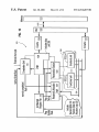
Referring to FIG. 10, a block diagram of a superscalar
processor as described above is shoWn for the preferred
embodiment of the invention. (Note that herein a numbered
element is numbered according to the ?gure in Which the
element is introduced, and is referred to by that number
throughout succeeding ?gures.) Processor 910 has a bus
interface unit 1002 coupled to the bus 912 for controlling
RID=Rename buffer ID, this ID points to the location in
the rename buffer to Which this instruction RT is assigned.
Y=young bit, this bit indicates the youngest RT in this
rename table. If Y=1, then this RT is youngest.
R=data in rename buffer bit. When R=1, then the data is
35
transfers of data and instructions betWeen memory, such as
random access memory 914, and caches 1004 and 1006.
Instructions are processed in processor 910 in a sequence
in the rename buffer. When R=0, then the data is in one of
the execution units.
V=entry valid bit. When V=1, then the data is being
renamed (it could either be in the rename buffer or in one of
the execution units). When V=0, then the data is in the
architected register ?le.
of logical, pipelined stages, as has been previously
described; hoWever, it should be understood that some of the
functions of these stages, as implemented in the preferred
CAM=Content Addressable Memory (i.e. read by
compares) Regular RID Allocation=this logic allocates one
embodiment, may be merged together, so that this particular
of the rename buffer to an instruction that being issued by
division of stages should not be taken as a limitation, unless
a such limitation is indicated in the claims herein. Indeed, 45 the instruction queue. It may have P entries.
Over?oW RID=this logic allocates one rename buffer to
some of the previously described stages are indicated as a
the instruction being issued if this instruction is the next
instruction to be completed AND the RID Allocation logic
is full. If the RID Allocation is un?lled, then the said
instruction Will be renamed by the RID Allocation logic. It
contains 1 entry.
single logic unit 1008 in FIG. 10 for the sake of simplicity
of understanding and because each distinction betWeen
stages is not necessarily central to the present invention.
Logic 1008 in FIG. 10 includes dispatch unit 305, fetch,
branch processing, instruction buffer, and decode units. The
logic 1008 fetches instructions from instruction cache 1004
Referring noW to FIG. 3, When an instruction is
dispatched, entries are created for the instruction in the
rename table 310 and the instruction queue (aka “IQ” or
into the instruction buffer, either based on a knoWn sequence
of the instructions or, in the case of a sequence having a
decodes the instructions and dispatches them to a reservation
station 1010, Which includes an instruction queue 330 from
Which the instructions are issued to appropriate functional
“Issue Queue”). That is, the instruction’s RT is Written into
the rename table 310, its op code is Written into the IQ 330,
and its IID is Written into both the rename table and the IQ.
The RT and IID ?elds are taken directly from the instruction
from dispatch. The R bit is set to 0 to indicate that the
instruction has not been executed yet, and the data Will be in
units 1012.0, 1012.1, . . . 1012.n—1. In executing the
one of the execution units. The V bit is set to 1 to indicate
instructions, the units 1012 input and output information to
logic 1014 and IQ 330. The functional units 1012 signal the
completion unit 410 upon execution of instructions and the
completion unit 410 retires the instructions, Which includes
notifying allocation logic 320, rename buffer 414 and
that this instructions RT has been renamed, and the data is
not in the architected register. The Y bit for the rename table
entry is set to 1 to indicate that this RT is the youngest RT
?eld in the machine. The incoming RT is also used to search
the Whole rename table for other RT With the same values;
if there are RT matches, then the Y bits of the older RTs in
conditional branch instruction, a predicted sequence, the
55
predicted sequence being in accordance With addresses
selected by the branch processing unit. The logic 1008 also
rename table 310 in logic 1014. The functional units 1012
65
US 6,311,267 B1
7
8
the rename table is reset to 0. This Y bit is used When
multiple RTs With the same values are dispatched and the
source pointer for an operand, and it is pointing to one of the
location in the rename buffer). At the rename table, the
Finish ID Will be used to compare With all of the IIDs in the
rename table. At any matched location, the R bit Will set to
incoming instruction must know that it only depends on the
youngest RT in the machine.
In addition to the above reference information being
Written into the rename table 310 and the IQ 330, there is a
1 to indicate the data noW resides in the rename buffer. At
instruction dispatch time, the RID Will be read out and sent
to the IQ.
concurrent search of the RT ?eld of the rename table in order
to determine Where source data Will come from. That is,
there is a CAM 312 compare of the rename table RT ?eld
With the currently dispatching instruction’s source registers,
RA and RB, for example. At any matched locations, the Y bit
At instruction completion time, the Completion IID is
10
is examined. If there are multiple matches (i.e. there are
several RTs in the rename table that match the RA or RB
?elds), then the RT ?eld With the Y=1 is the true match. The
IID, RID, Y, R, and V bits from that location are read out and
15
sent to the instruction queue 330. Such a rename IID sent to
the IQ is stored in the DIID (dependent IID) ?eld in the IQ
for the currently dispatched instruction, since it identi?es an
instruction Which generates source data for the currently
issuing instruction having the IID in the rename table. Thus,
for an IID identi?ed instruction in the IQ, the one or more
RID’s in the IQ identify the one or more rename registers for
rename table Will be used to de-allocate a rename buffer
entry and release that rename buffer entry to the RID
allocation logic. The neWly released RID noW can be
assigned to a younger instruction.
source operands, and the Y, V and R bits in the IQ describe
the status of the respective instructions generating such
source operands.
Once dispatched to the IQ, an instruction is checked to see
if all of its operands are available. If all of its operands are
available, and if it is selected to be issued for execution, then
its RT (target register) is assigned an RID if the rename
buffer is un?lled. If the rename buffer is full, then the target
register cannot be renamed, and the instruction Will not be
issued for execution and Will be held in the IQ until the
rename buffer becomes un?lled and starts assigning RID
25
First, in FIG’s 5 and 6, steps are shoWn associated With
dispatching and issuing of instructions.
Responsive to instruction dispatch, at 510, entries are
created in the rename table and IQ, Wherein certain
parameters, as shoWn at 550, are Written to the rename table
and the IQ. Also, the rename table is read, via CAM, to ?nd
target registers corresponding to the instruction’s target
35
registers matching the instruction target registers.
Also responsive to instruction dispatch, at 510, source
operands are looked up. That is, the rename table is read, via
Rename Over?oW Buffer 322 is employed in RID
Allocation/Deallocation Logic 320. According to the
Allocation/Deallocation Logic 322, When an instruction is
CAM, to ?nd the youngest target register corresponding to
still in the IQ and the regular rename buffer is full and it is
45
then the Rename Over?oW Buffer 322 Will assign a RID to
this instruction to alloW it to execute. HoWever, if an
instruction is still in the IQ and it is next to be completed but
an instruction, it Will send back the Finish IID of the
instruction that it Was Working on to the IQ and the rename
table. At the IQ, the Finish IID Will be used to compare With
all of the DIIDs in the IQ. At any matched location, the R bit
the source registers, at 520. A match not being found for a
source register means that the source operand has been
computed already, i.e., the instruction that generates the
source data has complete, and the data is noW in the
architected register.
the regular rename buffer is un?lled, then the Regular RID
Allocation logic Will assign it a RID (this RID Will be called
allocated-RID). The IID of the instruction that is being
issued (this IID Will be called issuing-IID) Will be sent to
both the IQ and the rename table. At the IQ, the issuing IID
execute. When the execution engine 340 ?nishes executing
the logic branches to 554, Where the target register Y bits are
logic branches to 556, Where no further steps are required
responsive to the search in the rename table for target
unable to execute for lack of a rename register. Therefore,
Will be used to compare With all of the DIIDs in the IQ and
at any matched location, the allocated-RID Will be latched
in. At the rename table, the issuing-IID Will be used to
compare With all of the IlDs in the rename table and at any
matched location, the allocated-RID Will be latched in.
After receiving a RID, the instruction is alloWed to
registers, at 550. If there are any matches, as indicated at 552
reset to 0. If there are no matches, as indicated at 552 the
buffers, the oldest instruction in the machine Would be
next to be completed (i.e. oldest instruction in the machine),
Referring noW to FIG’s 5 through 8, logical steps for the
exemplary embodiment are illustrated in a How chart format.
again.
A deadlock issue arises because of a potential execution
race among instructions. That is, if younger instructions
execute before the older instruction can execute, and the
younger instructions thereby consume all available rename
sent out by the completion unit 410 to the IQ 330, rename
table 310, and RID de-allocation logic 320. At the IQ, the
Completion IID is used to compare With all of the DIIDs in
the IQ. At any matched location, the V bit of that operand
Will be reset to 0 to indicate that the data for this operand is
noW residing in the architected register ?le (note: this V bit
is not the instruction queue entry valid bit). At the rename
table, the Completion IID is used to compare With all of the
IlDs in the rename table. At any matched location, the V bit
Will be reset to 0 to indicate that the data for this operand is
noW residing in the architected register ?le. At the RID
de-allocation logic, the RID that Was read out from the
55
If a match is not found, at 525, then the logic branches to
Wait for readiness to issue the instruction, at 540. For
example, there may be a Wait for an available execution unit
before the instruction may be issued.
If a match is found at 525, certain parameters, as shoWn
at 530, are read from the rename table and sent to the IQ. At
532, there is a check to see if R=1, indicating the target
register data is available. If the data is ready, then the logic
branches to Wait for readiness to issue the instruction, at 540.
If not, there is snooping for the data at 534, until the
snooping hits, at 536, at Which point the logic branches to
Wait for readiness to issue the instruction, at 540.
Once an instruction is ready for issue, i.e., its source
operands are available and an execution unit is available, the
rename buffer is checked, at 560. If full, then the over?oW
rename buffer is checked, at 562. If the over?oW rename
Will set to 1 to indicate the data is noW residing in the rename 65 buffer is full, the logic returns to 540 to Wait for a rename
register to become available. If the over?oW rename buffer
buffer. At instruction issue time, the RID Will be used to
is not full, the instruction is checked to see if it is the oldest
access the rename buffer to get its data (i.e. RID is noW the
US 6,311,267 B1
9
10
dispatched instruction, at 564. If not, the logic returns to 540
then the V bit is set to 0 for the matching entries in the IQ,
to Wait for a rename register to become available. If it is the
oldest dispatched instruction, or if the regular renarne buffer
as indicated at 840. This indicates that the instruction’s
result is in the architected register noW, instead of the renarne
Was not full at 560, then a neW RID is assigned to the
register.
dispatched and noW issuing instruction.
Once the RID is assigned, the instruction is issued, as
At 850 the completion IID is used to compare With IID’s
in the renarne table. A check for matches is done (not
shoWn). If no match, then no further step is required respon
indicated at 570, and further steps are taken in connection
With the issuing, as indicated in FIG. 6. Referring noW to
FIG. 6, once the RID is assigned, at 566, then the RID
allocated to the issuing instruction, and the instruction’s IID
sive to comparing in the IQ at this point (not shoWn). If there
10
are broadcast to the IQ and rename table, at 610. The issued
IID is used, at 620, to compare With DIID’s in the IQ. If there
is a match, as indicated at 625, the logic branches and the
allocated RID is Written, as shoWn at 635, in the IQ at the
matching locations. Thus, the IQ is thereby provided With
Also at 855, one or more RT and RID are read out at the
15
the identity of renarne registers for source operands. If there
is no match, then, as indicated at 630, no further steps are
presently needed responsive to the cornparing of the issued
IID With DIID’s in the IQ.
Also responsive to the RID and IID being broadcast to the
IQ and rename table, at 610, the issued IID is used, at 640,
to compare With IID’s in the renarne table. If there is a
25
thereby provided With the identity of renarne registers for
destination operands. If there is no match, then, as indicated
at 650, no further steps are presently needed responsive to
the cornparing of the issued IID With IID’s in the renarne
table.
Referring noW to FIG. 7, steps are shoWn associated With
executing the instruction. The execution function is shoWn
assigning, to a dispatched instruction having a target
register, a renarne register from among a plurality of
renarne registers, Wherein the assigning of a renarne
register includes assigning the renarne register in
response to availability of source operands for the
35
dispatched instruction.
2. The method of claim 1, Wherein the renarne registers
are of a ?rst and second type, and the assigning of a renarne
register includes assigning the ?rst type of renarne register
no match is found, as shoWn at 740, then no further action
in response to availability of the ?rst type of renarne register.
3. The method of claim 2, Wherein the instructions have
a program order, and the dispatching includes dispatching
the instructions in their program order, and Wherein the
is required at this point responsive to the checking for a
match in the IQ. If a match is found, as shoWn at 745, then
the R bit is set to 1 for the matching locations in the IQ,
indicating that the instruction’s result for the corresponding
IQ entry is noW in its renarne register.
LikeWise, the ?nish IID is used, at 750, to compare With
IID’s in the renarne table. As shoWn at 755, a match is
checked. If no match is found, as shoWn at 758, then no
While the invention has been shoWn and described With
reference to particular embodiments thereof, it Will be
understood by those skilled in the art that the foregoing and
other changes in form and detail may be made therein
Without departing from the spirit and scope of the invention.
What is claimed is:
1. A method of assigning renarne registers to instructions
being processed in a processor, comprising the steps of:
dispatching instructions; and
as a starting point, at 710. The logic loops, at 720, checking
for the execution to be ?nished. Once ?nished, at 725, the
IID for the ?nished instruction is broadcast to the IQ and
rename table. The ?nish IID is used, at 730, to compare With
DIID’s in the IQ. As shoWn at 735, a match is checked. If
matching entry or entries and any RID is sent to the RID
allocation/deallocation logic and rename buffer.
At 858, once deallocation is complete the RID is released
for reuse. At 860, the RID is used to read cornpleted data
from the renarne buffer and send it to the architected register
?le, While the RT is used to determine Which of the archi
tected registers gets the completed data.
match, as indicated at 645, the logic branches, and the
allocated RID is Written, as shoWn at 660, in the renarne
table at the matching locations. Thus, the renarne table is
is a match, then the V bit is set to 0 for the matching entries
in the renarne table, as indicated at 855, Which indicates that
the instruction’s result is in the architected register noW.
method comprises the step of:
completing the instructions in program order, Wherein
45
each dispatched, non cornpleted instruction has an age
With respect to the other dispatched, non cornpleted
instructions, and Wherein in response to non availabil
further action is required at this point responsive to the
ity of the ?rst type of renarne register, the assigning of
checking for a ?nish IID match in the IQ. If a match is found,
as shoWn at 760, then the R bit is set to 1 for the locations
a renarne register includes assigning the second type of
renarne register in response to availability of the second
type of renarne register and the age of the instruction.
4. The method of claim 3, Wherein the assigning of the
second type of renarne register in response to the age of the
instruction includes assigning in response to the instruction
in the IQ, indicating that the instruction’s result for the
corresponding renarne table entry is noW in its renarne
register.
Once the instruction has executed, it is subject to comple
tion. Steps associated with completion are shoWn in FIG. 8.
The completion function is shoWn at 810, as a starting point.
At 820 the logic checks for readiness to complete, and Waits
55
tions.
5. The method of claim 4, Wherein the assigning of a
renarne register includes Waiting for availability of a renarne
register in response to i) all of the ?rst type of renarne
until the instruction is ready. Cornpletion requires that the
instruction be next in order of program sequence, and also,
for example, resolution of speculative execution. Once the
instruction is ready to complete, at 825, the completion IID
registers being assigned and the instruction being younger
than the oldest dispatched, non cornpleted instruction, or ii)
all of the second renarne registers being assigned and the
instruction being the oldest dispatched, non cornpleted
for the instruction is broadcast to the IQ, renarne table, and
RID allocation/deallocation logic.
At 830 the completion IID is used to compare With DIID’s
in the IQ. A check for matches is done at 835. If no match,
being the oldest of the dispatched, non cornpleted instruc
instruction.
then no further step is required responsive to comparing in
6. An apparatus for processing instructions, Wherein the
processing includes assigning renarne registers to certain of
the IQ at this point, as indicated at 838. If there is a match,
the instructions being processed, cornprising:
65
US 6,311,267 B1
11
12
a) means for dispatching instructions; and
b) means for assigning, to a dispatched instruction having
younger than the oldest dispatched, non completed
instruction, or ii) all of the second rename registers
a target register, a rename register from among a
being assigned and the instruction being the oldest
dispatched, non completed instruction.
11. An information handling system, comprising:
a) a memory for storing computer program instructions,
plurality of rename registers, Wherein the assigning
means includes:
b1) means for assigning the rename register in response
to availability of source operands for the dispatched
instruction.
7. The apparatus of claim 6, Wherein the rename registers
are of a ?rst and second type, and the assigning means b)
includes:
b2) means for assigning the ?rst type of rename register
in response to availability of the ?rst type of rename
the instructions having a program order; and
b) a processor, coupled to the memory, for receiving and
processing the instructions, comprising:
b1) a plurality of architected registers;
register.
8. The method of claim 7, Wherein the instructions have
a program order, and the dispatching means a) includes:
a1) means for dispatching the instructions in their pro
15
tination operands; and
b4) rename register allocation/deallocation logic, for
allocating and deallocating registers to the dis
patched instructions from among the plurality of
gram order; and Wherein the apparatus comprises:
instruction has an age With respect to the other
rename registers, Wherein such a rename register
stores one of its assigned instruction’s destination
25
type of rename register and the age of the instruc
tion.
9. The apparatus of claim 8, Wherein the assigning means
to a ?rst one of the dispatched instructions includes
assigning in response to a source operand for the ?rst
instruction being available in either: i) the rename
b4) means for assigning the second type of rename
register in response to the instruction being the oldest
register assigned by the allocation/deallocation logic
of the dispatched, non completed instructions.
10. The apparatus of claim 9, Wherein the assigning means
b5) means for Waiting for availability of a rename
register in response to i) all of the ?rst type of rename
registers being assigned and the instruction being
operands resulting from execution by the processor
until the rename register’s destination operand is
Written to its instruction’s designated architected
register, and Wherein the assigning of one of the
rename registers by the allocation/deallocation logic
b) includes:
b) includes:
number of the instructions identify ones of the archi
tected registers for respective source operands, and
ones of the architected registers for respective des
c) means for completing the instructions in program
order, Wherein each dispatched, non completed
dispatched, non completed instructions; and Wherein
the assigning means b) includes:
b3) means for assigning the second type of rename
register in response to unavailability of the ?rst
type of rename register, availability of the second
b2) a plurality of rename registers;
b3) a dispatch unit for dispatching the instructions
received from the memory, the instructions specify
ing operations for the processor, and Wherein a
for a destination operand of a second one of the
35
instructions, or ii) one of the architected registers
designated by the second instruction for the destina
tion operand of the second instruction.
*
*
*
*
*