1
In-circuit Simulator Board User’s Manual N O N - D I S C L O S U R E M68ICS08KX A G R E E M E N T R E Q U I R E D M68ICS08KXUM/D User’s Manual Important Notice to Users While every effort has been made to ensure the accuracy of all information in this document, Motorola assumes no liability to any party for any loss or damage caused by errors or omissions or by statements of any kind in this document, its updates, supplements, or special editions, whether such errors are omissions or statements resulting from negligence, accident, or any other cause. Motorola further assumes no liability arising out of the application or use of any information, product, or system described herein: nor any liability for incidental or consequential damages arising from the use of this document. Motorola disclaims all warranties regarding the information contained herein, whether expressed, implied, or statutory, including implied warranties of merchantability or fitness for a particular purpose. Motorola makes no representation that the interconnection of products in the manner described herein will not infringe on existing or future patent rights, nor do the descriptions contained herein imply the granting or license to make, use or sell equipment constructed in accordance with this description. Trademarks This document includes these trademarks: Motorola and the Motorola logo are registered trademarks of Motorola, Inc. Windows and Windows 95 are registered trademarks of Microsoft Corporation in the U.S. and other countries. Intel is a registered trademark of Intel Corporation. Motorola, Inc., is an Equal Opportunity / Affirmative Action Employer. For an electronic copy of this book, visit Motorola’s web site at http://mcu.motsps.com/documentation © Motorola, Inc., 2000; All Rights Reserved User’s Manual 2 M68ICS08KX In-circuit Simulator Board MOTOROLA Table of Contents User’s Manual — M68ICS08KX In-Circuit Simulator Table of Contents Section 1. General Information 1.1 Introduction. . . . . . . . . . . . . . . . . . . . . . . . . . . . . . . . . . . . . . . . . . . . . . 7 1.2 1.2.1 1.2.2 KXICS Components . . . . . . . . . . . . . . . . . . . . . . . . . . . . . . . . . . . . . . 11 KXICS Hardware . . . . . . . . . . . . . . . . . . . . . . . . . . . . . . . . . . . . . . 12 ICS Interface Software. . . . . . . . . . . . . . . . . . . . . . . . . . . . . . . . . . 12 1.3 Hardware and Software Requirements . . . . . . . . . . . . . . . . . . . . . . . . 13 1.4 Specifications . . . . . . . . . . . . . . . . . . . . . . . . . . . . . . . . . . . . . . . . . . . 13 1.5 About This Manual . . . . . . . . . . . . . . . . . . . . . . . . . . . . . . . . . . . . . . . 13 1.6 Customer Support . . . . . . . . . . . . . . . . . . . . . . . . . . . . . . . . . . . . . . . . 13 Section 2. Preparation and Installation 2.1 Introduction. . . . . . . . . . . . . . . . . . . . . . . . . . . . . . . . . . . . . . . . . . . . . 15 2.2 Hardware Preparation . . . . . . . . . . . . . . . . . . . . . . . . . . . . . . . . . . . . . 15 2.2.1 KXICS Limitations . . . . . . . . . . . . . . . . . . . . . . . . . . . . . . . . . . . . 15 2.2.2 Configuring the KXICS Jumper Headers . . . . . . . . . . . . . . . . . . . 16 2.2.3 Installing an MCU on the KXICS . . . . . . . . . . . . . . . . . . . . . . . . . 17 2.2.4 Connecting the KXICS to the host PC. . . . . . . . . . . . . . . . . . . . . . 18 2.2.5 Applying power to the KXICS. . . . . . . . . . . . . . . . . . . . . . . . . . . . 19 2.2.6 Target Cable Interface Connection Options. . . . . . . . . . . . . . . . . . 19 2.3 Target Cable Interface Connectors . . . . . . . . . . . . . . . . . . . . . . . . . . . 20 2.3.1 Host Computer - KXICS Interconnection J6 . . . . . . . . . . . . . . . . . 23 2.3.2 Power Connector J2 . . . . . . . . . . . . . . . . . . . . . . . . . . . . . . . . . . . . 23 2.4 Connecting the KXICS . . . . . . . . . . . . . . . . . . . . . . . . . . . . . . . . . . . . 24 2.5 Connecting the KXICS to the Target System . . . . . . . . . . . . . . . . . . . 24 2.6 Installing the Software . . . . . . . . . . . . . . . . . . . . . . . . . . . . . . . . . . . . 25 M68ICS08KX In-Circuit Simulator MOTOROLA User’s Manual Table of Contents 3 Table of Contents Section 3. Support Information 3.1 Introduction. . . . . . . . . . . . . . . . . . . . . . . . . . . . . . . . . . . . . . . . . . . . . 27 3.2 MCU Subsystem . . . . . . . . . . . . . . . . . . . . . . . . . . . . . . . . . . . . . . . . . 27 3.3 Level Translation . . . . . . . . . . . . . . . . . . . . . . . . . . . . . . . . . . . . . . . . 28 3.4 KXICS Theory of Operation. . . . . . . . . . . . . . . . . . . . . . . . . . . . . . . . 28 3.4.1 Power Supply . . . . . . . . . . . . . . . . . . . . . . . . . . . . . . . . . . . . . . . . . 28 3.4.2 Serial Communications . . . . . . . . . . . . . . . . . . . . . . . . . . . . . . . . . 30 3.4.3 Clock Selection . . . . . . . . . . . . . . . . . . . . . . . . . . . . . . . . . . . . . . . 30 3.4.4 Start-Up in Monitor Mode . . . . . . . . . . . . . . . . . . . . . . . . . . . . . . . 31 3.5 3.5.1 3.5.2 3.5.3 3.5.4 3.5.5 KXICS Connector Signal Definitions. . . . . . . . . . . . . . . . . . . . . . . . . 32 Target Flex Cable Interface Connector J1 . . . . . . . . . . . . . . . . . . . 32 Target Ribbon Interface Connector J5 . . . . . . . . . . . . . . . . . . . . . . 33 Target MONO8 Interface Connector J3. . . . . . . . . . . . . . . . . . . . . 34 Power Connector . . . . . . . . . . . . . . . . . . . . . . . . . . . . . . . . . . . . . . 35 RS-232C Communication Connector, J6. . . . . . . . . . . . . . . . . . . . 36 3.6 Parts List . . . . . . . . . . . . . . . . . . . . . . . . . . . . . . . . . . . . . . . . . . . . . . . 37 3.7 KXICS Board Layout and Schematics Diagrams. . . . . . . . . . . . . . . . 40 Section 4. Using the MON08 Interface 4.1 Introduction. . . . . . . . . . . . . . . . . . . . . . . . . . . . . . . . . . . . . . . . . . . . . 41 4.2 Target System Header Placement and Layout . . . . . . . . . . . . . . . . . . 41 4.3 Connecting to the In-Circuit Simulator . . . . . . . . . . . . . . . . . . . . . . . 42 Appendix A. S-Record Information A.1 Introduction. . . . . . . . . . . . . . . . . . . . . . . . . . . . . . . . . . . . . . . . . . . . . 43 A.2 S-Record Contents . . . . . . . . . . . . . . . . . . . . . . . . . . . . . . . . . . . . . . . 43 A.3 S-Record Types. . . . . . . . . . . . . . . . . . . . . . . . . . . . . . . . . . . . . . . . . . 44 A.4 S Record Creation . . . . . . . . . . . . . . . . . . . . . . . . . . . . . . . . . . . . . . . . 45 A.5 S-Record Example . . . . . . . . . . . . . . . . . . . . . . . . . . . . . . . . . . . . . . . 45 A.5.1 S0 Header Record . . . . . . . . . . . . . . . . . . . . . . . . . . . . . . . . . . . . . 46 User’s Manual 4 M68ICS08KX In-Circuit Simulator Table of Contents MOTOROLA Table of Contents A.5.2 A.5.3 A.5.4 First S1 Record. . . . . . . . . . . . . . . . . . . . . . . . . . . . . . . . . . . . . . . . 46 S9 Termination Record . . . . . . . . . . . . . . . . . . . . . . . . . . . . . . . . . 47 ASCII Characters . . . . . . . . . . . . . . . . . . . . . . . . . . . . . . . . . . . . . . 48 Appendix B. Quick Start Hardware Configuration Guide B.1 Introduction. . . . . . . . . . . . . . . . . . . . . . . . . . . . . . . . . . . . . . . . . . . . . 49 B.1.1 KXICS Configurable Jumper Headers. . . . . . . . . . . . . . . . . . . . . . 50 B.1.2 Target Interface Cable Connections. . . . . . . . . . . . . . . . . . . . . . . . 51 B.1.3 Host Computer — KXICS Interconnection (J6) . . . . . . . . . . . . . . 51 B.2 Installing the Hardware. . . . . . . . . . . . . . . . . . . . . . . . . . . . . . . . . . . . 52 B.3 Installing the Software . . . . . . . . . . . . . . . . . . . . . . . . . . . . . . . . . . . . 53 B.4 Connecting to a Target System . . . . . . . . . . . . . . . . . . . . . . . . . . . . . . 53 Glossary M68ICS08KX In-Circuit Simulator MOTOROLA User’s Manual Table of Contents 5 Table of Contents User’s Manual 6 M68ICS08KX In-Circuit Simulator Table of Contents MOTOROLA List of Figures User’s Manual — M68ICS08KX In-Circuit Simulator List of Figures Figure 1-1 2-1 2-2 2-3 3-1 Title Motorola M68ICS08KX (KXICS) Board . . . . . . . . . . . . . . . . . . . . . 12 KXICS with SOIC-to-DIP Adapter . . . . . . . . . . . . . . . . . . . . . . . . . . 23 Host Computer to KXICS Interconnection . . . . . . . . . . . . . . . . . . . . 28 J2 Power Connector . . . . . . . . . . . . . . . . . . . . . . . . . . . . . . . . . . . . . . 28 KXICS Board Layout . . . . . . . . . . . . . . . . . . . . . . . . . . . . . . . . . . . . 44 M68ICS08KX In-Circuit Simulator MOTOROLA Page User’s Manual List of Figures 7 List of Figures User’s Manual 8 M68ICS08KX In-Circuit Simulator List of Figures MOTOROLA List of Tables User’s Manual — M68ICS08KX In-Circuit Simulator List of Tables Table Title Page Table 1-1. KXICS Product Components . . . . . . . . . . . . . . . . . . . . . . . . . . . . 15 Table 1-2. Hardware Connector Components . . . . . . . . . . . . . . . . . . . . . . . . 16 Table 1-3. Software Components . . . . . . . . . . . . . . . . . . . . . . . . . . . . . . . . . . 16 Table 1-4. KXICS Board Specifications. . . . . . . . . . . . . . . . . . . . . . . . . . . . . 17 Table 2-1 KXICS Jumper Header Description . . . . . . . . . . . . . . . . . . . . . . . . 21 Table 2-2. Cable/Connector Options for MCUs . . . . . . . . . . . . . . . . . . . . . . . 23 Table 2-3 J1 Pin Assignments . . . . . . . . . . . . . . . . . . . . . . . . . . . . . . . . . . . . 24 Table 2-4 J5 Pin Assignments . . . . . . . . . . . . . . . . . . . . . . . . . . . . . . . . . . . . 25 Table 2-5 J3 Pin Assignments . . . . . . . . . . . . . . . . . . . . . . . . . . . . . . . . . . . . 26 Table 3-1 J1 Target Flex Connector Pin Assignments . . . . . . . . . . . . . . . . . . 36 Table 3-2 J5 Target Connector Pin Assignments . . . . . . . . . . . . . . . . . . . . . . 38 Table 3-3 J3 MONO8 Target Connector Pin Assignments . . . . . . . . . . . . . . 39 Table 3-4 Power Connector J2 Pin Assignments . . . . . . . . . . . . . . . . . . . . . . 39 Table 3-5 RS-232C Communication Connector J6 Pin Assignments . . . . . . 40 Table 3-6. KXICS Parts List (Rev F) . . . . . . . . . . . . . . . . . . . . . . . . . . . . . . 41 Table 4-1. MON08 Target System Connector J3 . . . . . . . . . . . . . . . . . . . . . . 45 Table 4-2 KXICS Jumper Header Description . . . . . . . . . . . . . . . . . . . . . . . . 54 Table 4-3 Cable/Connector Options for MCUs . . . . . . . . . . . . . . . . . . . . . . . 55 M68ICS08KX In-Circuit Simulator MOTOROLA User’s Manual List of Tables 9 List of Tables User’s Manual 10 M68ICS08KX In-Circuit Simulator List of Tables MOTOROLA User’s Manual — M68ICS08KX In-Circuit Simulator Section 1. General Information 1.1 Introduction This section provides general information about the Motorola M68ICS08KX in-circuit simulator (KXICS). The KXICS board (Figure 1-1) is a stand-alone development and debugging tool. It contains the hardware and software needed to develop and simulate source code and to program Motorola’s MC68HC908KX8 microcontroller (MCU). The KXICS and it’s software form a complete editor, assembler, programmer, simulator, and limited real-time input/output emulator for the MCU. When connection is made between a host PC (personal computer) and target hardware (your prototype product), actual inputs and outputs of the target system may be used during code simulation. The KXICS can interface with any IBM Windows 95-based computer (or later version) through connection of a single RS-232 serial port using a DE-9 serial cable. Connection to the target system is accomplished by a ribbon cable, a Motorola M68CLB05A flex cable, or a MONO8 cable. The ribbon cable or flex cable is used when an MCU is resident on the KXICS for emulation or simulation, and the MONO8 cable is used to debug or program a target system’s MCU, directly, when the MCU resides on the target hardware. M68ICS08KX In-Circuit Simulator MOTOROLA User’s Manual General Information 11 General Information Figure 1-1 Motorola M68ICS08KX (KXICS) Board The KXICS is a low-cost development system that supports editing, assembling, in-circuit simulation, in-circuit emulation, and FLASH memory programming. Its features include: • Editing with WinIDE • Assembling with CASM08W • Programming FLASH memory with PROG08SZ • Simulating in-circuit and stand-alone MC68HC908KX8 MCU with ICS08KXW software, providing: • – Simulation of all instructions, memory, and peripherals – Simulation of pin inputs from the target system – Installation of conditional breakpoints, script files, and logfiles Debugging and emulation (limited real-time) with ICD08SZ, including: User’s Manual 12 M68ICS08KX In-Circuit Simulator General Information MOTOROLA General Information Introduction – Loading code into RAM – Executing real-time in RAM or FLASH – Placing one hardware breakpoint in FLASH – Placing multiple breakpoints in RAM • On-line help documentation for all software • Software integrated into the WinIDE environment, allowing function key access to all applications • MON08 emulation connection to the target system allowing: • – In-circuit emulation – In-circuit simulation – In-circuit programming Four modes of operation: – Standalone — using the KXICS as a standalone system without a target board – Simulation — using the KXICS as an in-circuit simulator/emulator with a target cable – Evaluation - using the KXICS for real-time evaluation of the MCU and to debug user developed hardware and software – Programming — using the KXICS as a programmer • With the ICD08SZ debugging software, code can be run directly out of the MCU’s internal FLASH at real-time speeds. • With the WinIDE, CASM08Z, editor, simulator, and assembler software, the function is as a limited real-time emulator. • With the PROG08SZ software, the function is to program MCU FLASH memory. • With the ICS08KXZ simulation software, the MCU provides the required input/output information that lets the host computer simulate code, performing all functions except for maintaining port values. (The internal FLASH memory on the device is downloaded with a program that generates the appropriate port values.) The ICS08KXZ software on the host computer lets the host computer become a simulator. M68ICS08KX In-Circuit Simulator MOTOROLA User’s Manual General Information 13 General Information • With using the ICD08SZ debugging software, code can be run directly out of the MCU’s internal FLASH at real-time speeds. • Timing is accomplished with a 9.8304 MHz crystal User’s Manual 14 M68ICS08KX In-Circuit Simulator General Information MOTOROLA General Information KXICS Components 1.2 KXICS Components The complete KXICS system includes hardware, software, and documentation. lists the KXICS product components. Table 1-1. KXICS Product Components Part Number Description ICS08KX KXICS software development package ICS08KXZ KXICS software simulator ICD08SZ KXICS software debugger/emulation MC68HC908KX8CP MCU (16-pin DIP package) MC68HC908KX8CDW MCU (16-pin SOIC Package) PA16SO-08H-3 SOIC-to-DIP Socket Adapter M68CLB05A Flex target cable KRISTA 22-122 Serial cable FRIWO 11.8999-P5 Power supply M68ICS08SOM/D In-circuit simulator software operator’s manual M68ICS08KXHOM/D In-circuit simulator hardware operator’s manual M68ICS08KX In-Circuit Simulator MOTOROLA User’s Manual General Information 15 General Information 1.2.1 KXICS Hardware lists the KXICS hardware components. Table 1-2. Hardware Connector Components Components Description Test socket for the Motorola MC68HC908KX8 MCU: 16-pin DIP (dual in-line package) XU1 J1 Two 2-row × 20-pin, 0.1-inch spacing connectors to connect the KXICS to a target using the M68CLB05A flex cable J2 +5 Vdc input voltage (VDD) J3 One 2-row × 8-pin, 0.1-inch spacing connector to connect to a remote target via the MON08 debug circuit. J4 J4 is the clock output that may be used for synchronizing a target or test equipment to the KXICS clock. J5 One 2-row × 8-pin, 0.3-inch spacing dual in-line package (DIP) socket to allow the KXICS to be connected to the target using a ribbon cable J6 RS-232 to interface KXICS to host computer serial connector (DEKL-9SAT-F) 1.2.2 ICS Interface Software Windows-optimized software components are referred to, collectively, as the KXICS software (part number ICS08KX). It is a product of P&E Microcomputer Systems, Inc. and is included in the KXICS kit (). Table 1-3. Software Components Components Description WINIDE.EXE Integrated development environment (IDE) software interface for editing and performing software or in-circuit simulation CASM08Z.EXE CASM08Z command-line cross-assembler ICS08SZ.EXE In-circuit/stand-alone simulator software for the MC68HC908KX8 MCU PROG08SZ.EXE FLASH memory programming software ICD08SZ.EXE In-circuit debugging software for limited, real-time emulation User’s Manual 16 M68ICS08KX In-Circuit Simulator General Information MOTOROLA General Information Hardware and Software Requirements 1.3 Hardware and Software Requirements The KXICS software requires this minimum hardware and software configuration: • Windows 95 or later version operating system • Approximately 2 Mbytes of available random-access memory (RAM) and 5 Mbytes of free disk space • A serial port for communications between the KXICS and the host computer 1.4 Specifications Table 1-4 summarizes the KXICS hardware specifications. Table 1-4. KXICS Board Specifications Characteristic Specification Temperature: Operating Storage 0° to 40°C –40° to +85°C Relative humidity 0 to 95%, non-condensing Power requirement +5 Vdc, from included ac/dc adapter 1.5 About This Manual The procedural instructions in this manual assume that the user is familiar with the Windows interface and selection procedures. 1.6 Customer Support To obtain information about technical support or ordering parts, call the Motorola help desk at 800-521-6274. M68ICS08KX In-Circuit Simulator MOTOROLA User’s Manual General Information 17 General Information User’s Manual 18 M68ICS08KX In-Circuit Simulator General Information MOTOROLA User’s Manual — M68ICS08KX In-Circuit Simulator Section 2. Preparation and Installation 2.1 Introduction This section provides information and instruction for configuring, installing, and readying the M68ICS08KX (KXICS) for use. 2.2 Hardware Preparation ESD CAUTION: Ordinary amounts of static electricity from clothing or the work environment can damage or degrade electronic devices and equipment. For example, the electronic components installed on the printed circuit board are extremely sensitive to electrostatic discharge (ESD). Wear a grounding wrist strap whenever handling any printed circuit board. This strap provides a conductive path for safely discharging static electricity to ground. 2.2.1 KXICS Limitations These sub-paragraphs describe system limitations of the KXICS. 2.2.1.1 Bus Frequency The KXICS communicates using the MON08 features which forces the communication rate to fbus/256, and the bus frequencies are limited by standard baud rates allowed by the host software. 2.2.1.2 Port A0 Port A0 is used for communications, so it is unavailable for emulation. M68ICS08KX In-Circuit Simulator MOTOROLA User’s Manual Preparation and Installation 19 Preparation and Installation 2.2.1.3 Low Voltage Interrupt (LVI) The LVI is disabled by default in monitor mode. It is enabled by a dummy write to LVISR. 2.2.1.4 Internal Clock Generator (ICG) The ICG is bypassed in monitor mode, so it is not available for use. 2.2.2 Configuring the KXICS Jumper Headers The KXICS supports four configuration options: standalone, simulation, evaluation, and programming. • Standalone — ICS08KXZ.exe running on the host computer (the KXICS is not connected.) Emulation of the MCU CPU, registers, and I/O ports is done within the host computer environment. • Simulation — Host computer is connected to the KXICS via the RS-232 cable and ICS08KXZ.exe runs on the host computer, providing access to the M68HC(9)08KX MCU CPU internal registers and I/O ports. • Evaluation — Host computer is connected to the KXICS, and the KXICS is connected to the target system via the flex cable, providing limited real-time evaluation of the MCU and debugging user developed hardware and software. • Programming — Host computer is connected to the KXICS, and the KXICS is connected to the target system via the MON08 cable with PROG08SZ.exe used to program the MCU FLASH module. In the programming mode there is limited evaluation (port A0 on the KX8 and port B0 and port B1 on the KX8 are used for communications, so they are unavailable for emulation). Four jumper headers (Table 2-1) on the KXICS are used to configure the hardware options. CAUTION: The KXICS can be set to operate at a variety of voltages. When configuring the KXICS jumper headers, care must be exercised to ensure that the voltages selected for the board match those of the target device. Failure to do so can result in damage to either or both of the pieces of equipment. User’s Manual 20 M68ICS08KX In-Circuit Simulator Preparation and Installation MOTOROLA Preparation and Installation Hardware Preparation Table 2-1 KXICS Jumper Header Description Jumper Header Type 1 2 W1 Low Voltage Select 12 11 W2 MCU Voltage Select 3 1 W3 Target Clock Select W4 PTB6 Select Description (Factory Default Shown 3 1 1 3 Used to set power for the MCU to match various target voltages.(No default) Jumper on position 1 & 2: 3.3 V Jumper on position 3 & 4: 3.0 V Jumper on position 5 & 6: 2.7 V Jumper on position 7 & 8 2.2 V Jumper on position 9 & 10 2.0 V Jumper on position 11 & 12: ADJ Selects voltage powering MCU and related circuitry. Jumper on position 1&2: Regulator Lo V as set by W1, is supplied by MCU. Labeled LO V. Jumper on position 3&2: Power supply, 5V Switched, is supplied by board to MCU. Labeled 5V. Jumper on position 1&2: supplies KXICS,9.8304 MHz, clock, to MCU and target via W4. Jumper on position 3&2: disables Xtal clock output, which will affect the power-up reset. Labeled 1. Jumper on position 1&2: MCU’s internal clock is supplied to target cable via PTB6. Jumper on position 3&2: KXICS Xtal clock is supplied to MCU. 2.2.3 Installing an MCU on the KXICS Either of two types of MCUs may be installed on the KXICS board, a DIP-type or a SOIC-type. 2.2.3.1 DIP-type MCU 1. Place the pin tension arm of the KXICS DIP socket XU1 in the up position. 2. Install the DIP type MCU into the DIP socket XU1. Be sure that the pin 1 orientation of the silkscreened dot on the MCU aligns with the pin 1 location on the DIP socket (upper left pin of the socket). M68ICS08KX In-Circuit Simulator MOTOROLA User’s Manual Preparation and Installation 21 Preparation and Installation 3. Place the pin tension arm of the KXICS DIP socket XU1 in the down position to secure the pins of the MCU to the socket. NOTE: The top (label side) of the MCU package must be visible when looking at the component side of the board. 2.2.3.2 SOIC-type MCU NOTE: Installation of a SOIC type MCU requires the use of the SOIC-to-DIP adapter identified in Table 1-1 of this manual. 1. Place the pin tension arm of the KXICS DIP socket XU1 (Figure 2-1) in the up position. 2. Install the SOIC-to-DIP adapter into the DIP socket XU1 (Figure 2-1). Be sure that the pin 1 orientation of the adapter aligns with the pin 1 location on the DIP socket (upper left pin of the DIP socket). CAUTION: The SOIC-to-DIP adapter may be confusing to install. It must be placed into the DIP socket, XU1, with the hinged side of the SOIC shell aligned to the bottom of the KXICS board. This positioning will place the SOIC-type MCU socket pin 1 in the upper left corner of the SOIC socket. 3. Place the pin tension arm of the KXICS DIP socket XU1 in the down position to secure the pins of the adapter to the socket. 4. Open the hinged access door on the SOIC shell. 5. Install the SOIC-type MCU into the SOIC socket of the adapter. Be sure that the pin 1 orientation of the silkscreened dot on the MCU aligns with the pin 1 location on the SOIC socket (upper left pin of the socket). 6. Close and secure the hinged access door on the SOIC shell. User’s Manual 22 M68ICS08KX In-Circuit Simulator Preparation and Installation MOTOROLA Preparation and Installation Hardware Preparation Figure 2-1 KXICS with SOIC-to-DIP Adapter 2.2.4 Connecting the KXICS to the host PC. Locate the 9-pin connector labeled J6 on the board. Using the cable provided, connect it to a serial COM port on the host PC. 2.2.5 Applying power to the KXICS. CAUTION: Although applying power is described here, do not apply power until all other configuring, installing, and cable connections are completed. Equipment damage can result. M68ICS08KX In-Circuit Simulator MOTOROLA User’s Manual Preparation and Installation 23 Preparation and Installation Connect the 5-volt power supply to the round connector on the board, J2. Plug the power supply into an ac power outlet, using one of the country-specific adapters provided. (The KXICS green power LED on the board lights when switch SW1 is in the ON position.) 2.2.6 Target Cable Interface Connection Options There are three ways to connect the KXICS simulator board to your target system: • Flex cable — low-noise target interface connection (may be ordered separately) • Ribbon cable — low-cost target interface connection • MON08 cable — target interface connection with MCU FLASH programming and limited emulation Below (Table 2-2) is a quick reference for defining the cable/connector selection to use with the MC68HC908KX8. Select the option that meets your requirements and connect accordingly. Table 2-2. Cable/Connector Options for MCUs MCU Flex Cable Ribbon Cable MON08 Cable J1 J5 J3 MC68HC908KX8 User’s Manual 24 M68ICS08KX In-Circuit Simulator Preparation and Installation MOTOROLA Preparation and Installation Target Cable Interface Connectors 2.3 Target Cable Interface Connectors NOTE: Refer to Section 3, Support Information for more detail. 2.3.0.1 Target Flex Cable Interface Connector J1 The flex cable is a low-noise alternative connection that may be used to connect to the target. Table 2-3 shows the pin assignments for flex cable connector J1. Table 2-3 J1 Pin Assignments J1 N/C 1 • • 2 N/C N/C 3 • • 4 PTB7 N/C 5 • • 6 PTB6 N/C 7 • • 8 PTB5 N/C 9 • • 10 PTB4 N/C 11 • • 12 N/C N/C 13 • • 14 PTB3 TGT_PTA0 15 • • 16 PTB2 TGT_PTA1 17 • • 18 TGT_PTB1 TGT_PTA2 19 • • 20 TGT_PTB0 TGT_PTA3 21 • • 22 N/C TGT_PTA4 23 • • 24 N/C N/C 25 • • 26 IRQ* N/C 27 • • 28 N/C Common 29 • • 30 Common Common 31 • • 32 Common Common 33 • • 34 Common Common 35 • • 36 Common Common 37 • • 38 Common Common 39 • • 40 Common M68ICS08KX In-Circuit Simulator MOTOROLA User’s Manual Preparation and Installation 25 Preparation and Installation 2.3.0.2 Target Ribbon Interface Connector J5 The KXICS includes a connector, J5 (Table 2-4), which allows a convenient, less-expensive connection to the target, using a 16-pin ribbon cable. Table 2-4 J5 Pin Assignments J5 Common 1 • • 16 N/CPTA1 PTA1 2 • • 15 PTA4 PTA0 3 • • 14 PTA3 IRQ* 4 • • 13 PTA2 PTB0 5 • • 12 PTB4 PTB1 6 • • 11 PTB6 PTB2 7 • • 10 OSC1/PTA3 PTB3 8 • • 9 PTB7 User’s Manual 26 M68ICS08KX In-Circuit Simulator Preparation and Installation MOTOROLA Preparation and Installation Target Cable Interface Connectors 2.3.0.3 Target MONO8 Interface Connector J3 The MONO8 interface connector, J3 (Table 2-5), is used when the MCU is mounted on the target. Refer to Section 4 Using the MONO8 for detailed information. Table 2-5 J3 Pin Assignments J4 RST_OUT* 1 • • 2 Common RST_IN* 3 • • 4 RST* TGT_IRQ* 5 • • 6 IRQ* TGT_PTA0 7 • • 8 PTA0 TGT_PTA1 9 • • 10 PTA1 TGT_PTB0 11 • • 12 PTB0 TGT_PTB1 13 • • 14 PTB1 N/C 15 • • 16 N/C M68ICS08KX In-Circuit Simulator MOTOROLA User’s Manual Preparation and Installation 27 Preparation and Installation 2.3.1 Host Computer - KXICS Interconnection J6 The host computer to KXICS interface is via the single system connector J6, which is a 9-pin, D-type connector (Amp part number AMP-9726-A) (Figure 2-2), mounted on the top side of the board. Connection requires the cable assembly supplied with your KXICS kit, a DB9-male-to-female, 6-ft. (3 m) long serial cable. 1 RXD 2 6 7 RTS TXD 3 8 DTR 4 9 GND 5 Figure 2-2 Host Computer to KXICS Interconnection 2.3.2 Power Connector J2 Connect +5-Vdc power directly to the KXICS via connector J2 (Figure 2-3) using the provided power supply. +5 Vdc GND Figure 2-3. J2 Power Connector User’s Manual 28 M68ICS08KX In-Circuit Simulator Preparation and Installation MOTOROLA Preparation and Installation Connecting the KXICS 2.4 Connecting the KXICS The following steps provide instructions for connecting the KXICS to the host PC and power connection. ESD CAUTION: Ordinary amounts of static electricity from clothing or the work environment can damage or degrade electronic devices and equipment. For example, the electronic components installed on the printed circuit board are extremely sensitive to electrostatic discharge (ESD). Wear a grounding wrist strap whenever handling any printed circuit board. This strap provides a conductive path for safely discharging static electricity to ground. a. Configure the jumpers W-1 through W-4 on the KXICS for your application. b. Install an MCU into the appropriate socket, XU1, on the KXICS board. NOTE: Observe the pin 1 orientation with the silkscreened dot. The top (label side) of the MCU package must be visible when looking at the component side of the board. c. Plug the serial cable into J6 on the KXICS. d. Plug the serial cable into the COM port on the host PC. NOTE: Steps e. through g. should not be completed until all connections to the target are completed (Paragraph 2.5). e. Connect the power cable to J2 on the KXICS board. f. Plug the power cable into an ac power outlet, using one of the country-specific adapters. g. The KXICS power LED lights green. 2.5 Connecting the KXICS to the Target System Connect the KXICS to the target system using one of these methods: • Emulating using a flex cable for low-noise M68ICS08KX In-Circuit Simulator MOTOROLA User’s Manual Preparation and Installation 29 Preparation and Installation When emulating, connect the 40-pin M68CLB05A flex cable to the connector labeled J1on the simulator board. Attach the other end of the cable to the appropriate connector on the target system. Target head adapters are available. • Emulating using a ribbon cable When emulating, connect a 16-pin flat ribbon cable to connector J5 on the simulator board. Attach the other end of the cable to the appropriate connector on the target system. • NOTE: Using a MON08 cable to debug the target system. An MCU must be installed in the target system. No MCU should on the KXICS. Connect the MON08 debug interface cable to the appropriate MON08 debug interface connector, J3, for communication with the target system’s MCU. Attach the other end of the cable to the appropriate connector on the target system. NOTE: For more detailed information on the MONO8, refer to Section 4 of this manual. 2.6 Installing the Software For instructions for installing the ICS08 software, refer to P&E Microcomputer Systems, Inc., M68ICS08 68HC08 In-Circuit Simulator Operator’s Manual, Motorola document order number M68ICS08OM/D. User’s Manual 30 M68ICS08KX In-Circuit Simulator Preparation and Installation MOTOROLA User’s Manual — M68ICS08KX In-Circuit Simulator Section 3. Support Information 3.1 Introduction This section includes data and information that may be useful in the design, installation, and operation of your application.\ 3.2 MCU Subsystem The MCU subsystem consists of the MC68HC908KX8 microcontroller, clock generation and selection, monitor mode control logic that places and holds the KXICS in monitor mode, the bus voltage level translation buffers, and processor operating voltage variable regulator. The MCU, an MC68HC908KX8, is available in two different packages: • 16-pin SOIC (small-outline integrated circuit) • 16-pin DIP (dual inline pack) Only one socket may be used at a time. M68ICS08KX In-Circuit Simulator MOTOROLA User’s Manual Support Information 31 Support Information Depending on the connection, the MCU is used in one of three operating modes: • In the KXICS socket for programming and simple simulation • In the KXICS socket and connected to the target for emulation • On the target for MON08 debug operation 3.3 Level Translation NOTE: For the following discussion on the theory of operation of the KXICS, refer to the schematic diagrams in Paragraph 3.6, Figures 3-1 to 3-6 of this section. The KXICS has an operation voltage range of +2.0 to +5.0 volts while the host development system interface is an RS-232 (COM) port. U12 on the ICS converts 5-volt logic signals to RS-232 levels. ICS U10–U13 translate 5-volt logic levels to the MCU operating voltage (2.0–3.3 volts). 3.4 KXICS Theory of Operation NOTE: For the following discussion on the theory of operation of the KXICS, refer to the schematic diagrams in Paragraph 3.7. 3.4.1 Power Supply Power input, J2, to the KXICS is via a standard DC power receptacle with a 2.5mm center pin. Input voltage is 5Vdc provided by a plug in the DC power adapter. The power is fused to prevent catastrophic failure by fuse F1 (5x20mm or 3AG fuse). CAUTION: Always use a fuse of the proper current and voltage rating. Failure to do so can result in serious equipment damage In addition, the input line has a Transient Voltage Suppression (TVS) diode to stop high voltage transients, including ESD events, from damaging the board. A green LED is provided to indicate that 5VDC is being provided to the board, with the ON/Off switch in the ON position. Power, however, is not available to User’s Manual 32 M68ICS08KX In-Circuit Simulator Support Information MOTOROLA Support Information KXICS Theory of Operation the rest of the board until the signal DTR is active high on pin 4 of the serial connector, J6. Test points are provided for common (TP1), power input VDD (TP3), switched main power VDD_SW (TP5), power to the MCU VDD_MCU (TP4), and VTST (TP2). 3.4.1.1 Main Switched Power Power to the MCU sockets and circuitry is switched on and off using the DTR signal into the serial interface (J6). When DTR is low, the power to the MCU socket is off, and the amber LED is off. When DTR is asserted high, transistor Q3 will turn on FET Q2 which provides power to the MCU circuitry. if W2 is selected positions 1 and 2. VTST voltage is sent to the MCU along with the reset signal being held low briefly following power-up. The MCU is forced to power-up in the Monitor Mode. NOTE: The source of power for the MCU is selected by jumper2. Refer to Section 2, Table 2-1. The amber LED, DS2, lights when there is power to the MCU socket. CAUTION: There is no over-current protection on the board protecting against catastrophic failures if the MCU is powered from the target. Equipment damage can result. The power to the MCU is selected by jumper W2. With the jumper in the 5V position, the MCU will be powered by the 5V circuitry, i.e., from the plug in the power supply). With W2 in the LO V position, the MCU will be powered by the on-board low voltage regulator (U6). The low voltage is selected by jumper W1 which has preset voltages of 3.3V, 3.0V, 2.7V, 2.2V, 2.0V, and a poteniometer for adjusting the voltage. CAUTION: The MCU may be set to operate at a variety of voltages. Ensure the selected voltage matches the voltage of the target. Failure to do so can result in equipment damage. M68ICS08KX In-Circuit Simulator MOTOROLA User’s Manual Support Information 33 Support Information 3.4.1.2 VTST Power VTST is created by a voltage regulator, MC34063, nominally set for 8.6VDC. This keeps the worst case voltage at greater than VDD +3VDC, meeting VTST voltage minimums. The voltage may be monitored at VTST test point TP2. VTST is used during start-up to force the MCU into the Monitor Mode. 3.4.1.3 Reset on Power-up At initial power-on to the MCU, there is a delay of a few hundred milliseconds during which the signal ICS_RST# is held low, as set by U8 (DS1233). When ICS_RST# goes high, the binary ripple counter, U3, begins counting clock cycles, at the 9.8304MHz rate of the clock Y1. After 1024 clock cycles are counted, the DELAY_RESET signal toggles and the counter stops counting. The delayed reset signal is used to turn-on communications to the MCU and to hold several MCU pins in appropriate states to force Monitor Mode on power-up. 3.4.2 Serial Communications Serial communication in half-duplex mode, using PTA0 for transmit and receive, to the MCU is via the DE9 connector, J6. Pin 2 is the path for transmit signals and pin 3 is for receive signals. Pin 4, the DTR signal, is utilized as an input to provide the software host with the ability to turn MCU power on and off. The RTS signal on contact 7 is used as an input to provide the software host with the ability to control the IRQ* high voltage. Serial communication to the MCU does not occur until DELAY_RESET becomes active high 1024 clock cycles after the RESET signal is high (para 3.4.1.3). 3.4.3 Clock Selection The source of timing for the MCU may be either the KXICS board’s clock Y1 or the MCU’S internal clock. Selection is by jumper header W-4 (Table 2-1). User’s Manual 34 M68ICS08KX In-Circuit Simulator Support Information MOTOROLA Support Information KXICS Theory of Operation When the jumper is set for the PTB6 position, the MCU runs from it’s internal clock and pin PTB6 of the MCU is connected to the target connector. When the jumper is set for the CLK position, the Y1 external clock signal from the KXICS board is applied to the PTB6 pin of the MCU for timing. (An internal MCU register must be set to control the selection of internal or external clock.) The external clock, Y1, has an output frequency of 9.8304 MHz to allow the MCU to communicate at 9600 baud. It is socketed to allow the use of a full-size or half-size clock. You may change clock frequencies by installing a new clock chip, however the serial communication rate proportionally changes. W3 may be used to disable the external clock. Additionally, the on-board clock is available as an output on the 3-pin header J4 for target or computer host clock synchronization. 3.4.4 Start-Up in Monitor Mode Following power up the ICS_RST# is held low for a period of time by U8. When ICS_RST* is asserted high, the binary ripple counter, U3, counts up 1024 clock cycles prior to allowing DELAY RESET to be asserted. The delayed reset controls the analog switch, U7, connected to PTA1 and PTB[0...1]. The RTS signal is held high which places the VTST voltage as the high voltage for IRQ*. Analog switch, U7, connects PTA1 to common, PTB0 to VDD_MCU, and PTB1 to common until DELAY_RESET is asserted. VTST is held above VDD-MCU +3Vdc during the reset release forcing the KXICS board to power up in the Monitor Mode. Following the counter time-out, the analog switch, U7, is toggled so that the PTA1 and PTB[0...1] pins of the board are connected to the target head connectors. Following entry into monitor mode, you may switch the IRQ* voltage to VDD_MCU by setting RTS low. The analog switch, U14, will switch the connection of MCU pin 9 from the ICS reset circuitry to a connection to the target head connector. Be aware that beside disabling the use of external resets of the MCU, internal MCU features, e.g., the COP must be serviced properly in this mode. M68ICS08KX In-Circuit Simulator MOTOROLA User’s Manual Support Information 35 Support Information 3.5 KXICS Connector Signal Definitions The tables in this section describe the pin assignments for the connectors on the KXICS board. 3.5.1 Target Flex Cable Interface Connector J1 Table 3-1 J1 Target Flex Connector Pin Assignments Pin No. Schematic NET 1 N/C 2 N/C 3 N/C 4 PTB7 5 N/C 6 PTB6 7 N/C 8 PTB5 9 N/C 10 PTB4 11 N/C 12 N/C 13 N/C 14 Direction Signal Description Bidirectional Port B I/O Bidirectional Port B I/O Bidirectional Port B I/O Bidirectional Port B I/O PTB3 Bidirectional Port B I/O 15 TGT_PTA0 Bidirectional Port A I/O 16 PTB2 Bidirectional Port B I/O 17 TGT_PTA1 Bidirectional Port A I/O 18 TGT_PTB1 Bidirectional Port B I/O 19 PTA2 Bidirectional Port A I/O 20 TGT_PTB0 Bidirectional Port B I/O 21 PTA3 Bidirectional Port A I/O 22 N/C User’s Manual 36 M68ICS08KX In-Circuit Simulator Support Information MOTOROLA Support Information KXICS Connector Signal Definitions Pin No. Schematic NET Direction 23 PTA4 Bidirectional 24 N/C 25 N/C 26 N/C 27 N/C 28 N/C 29 Common 30 Common 31 Common 32 Common 33 Common 34 Common 35 Common 36 Common 37 Common 38 Common 39 Common 40 Common Signal Description Port A I/O M68ICS08KX In-Circuit Simulator MOTOROLA User’s Manual Support Information 37 Support Information 3.5.2 Target Ribbon Interface Connector J5 The KXICS includes a connector, J5 (Table 3-2), which allows a convenient connection to the target, using a 16-pin ribbon cable. Table 3-2 J5 Target Connector Pin Assignments Pin No. Schematic NET 1 Common 2 PTA1 Bidirectional Port A I/O 3 PTA0 Bidirectional Port A I/O 4 IRQ* In 5 PTB0 Bidirectional Port B I/O 6 PTB1 Bidirectional Port B I/O 7 PTB2 Bidirectional Port B I/O 8 PTB3 Bidirectional Port B I/O 9 PTB7 Bidirectional Port B I/O 10 OSC1/PTB6 Bidirectional Clock signal from xtal or MCU/Port B I/O 11 PTB5 Bidirectional Port B I/O 12 PTB4 Bidirectional Port B I/O 13 PTA2 Bidirectional Port A I/O 14 PTA3 Bidirectional Port A I/O 15 PTA4 Bidirectional Port A I/O 16 VDD Direction Signal Description Target interrupt request to MCU KXICS Supply Voltage User’s Manual 38 M68ICS08KX In-Circuit Simulator Support Information MOTOROLA Support Information KXICS Connector Signal Definitions 3.5.3 Target MONO8 Interface Connector J3 The MONO8 interface connector, J3 (Table 2-6), is used when the MCU is mounted on the target. Refer to Section 4 Using the MONO8 for detailed information. Table 3-3 J3 MONO8 Target Connector Pin Assignments Pin No. Schematic NET Direction 1 RST_OUT* Out 2 Common 3 RST_IN* In 4 RST* Out 5 TGT_IRQ* In 6 IRQ* Out Interrupt Request 7 TGT_PTA0 Bidirectional Port A I/O - bit 0 8 PTA0 Bidirectional Port A I/O - bit 0 9 TGT_PTA1 Bidirectional Port A I/O - bit 1 10 PTB1 Bidirectional Port B I/O - bit 1 11 TGT_PTB0 Bidirectional Port B I/O - bit 0 12 PTB0 Bidirectional Port B I/O - bit 0 13 TGT_PTB1 Bidirectional Port B I/O - bit 1 14 PTB1 Bidirectional Port B I/O - bit 1 15 No connect 16 No connect Signal Description To reset target From target to reset MCU and Ripple Counters Forced reset to target Target Interrupt request to MCU 3.5.4 Power Connector Power connector, J2, (Table 3-4) is used to connect to a source power supply for the KXICS. Table 3-4 Power Connector J2 Pin Assignments Pin No. Mnemonic Signal 1 VCC +5 VDC POWER — Input voltage (+5 Vdc @ 1.0 A) from the provided power supply used by the KXICS logic circuits M68ICS08KX In-Circuit Simulator MOTOROLA User’s Manual Support Information 39 Support Information 3.5.4 Power Connector Power connector, J2, (Table 3-4) is used to connect to a source power supply for the KXICS. Table 3-4 Power Connector J2 Pin Assignments Pin No. Mnemonic 2 GND Common 3 GND Common Signal 3.5.5 RS-232C Communication Connector, J6 The RS-232C Communication Connector, J6, (Table 3-5) provides connection to the host computer. Table 3-5 RS-232C Communication Connector J6 Pin Assignments Pin No. Mnemonic 2 RXD RECEIVE DATA — Output for sending serial data to the DTE device 3 TXD TRANSMIT DATA — Input for receiving serial data output from the DTE device 4 DTR DATA TERMINAL READY — Switches the KXICS to apply power to the MCU and related circuitry 5 GND Common 7 RTS Controls whether voltage for IRQ* high is VTST or VDD_MCU. Signal User’s Manual 40 M68ICS08KX In-Circuit Simulator Support Information MOTOROLA Support Information Parts List 3.6 Parts List Table 3-6. KXICS Parts List (Rev F) Reference Designator Description Manufacturer Part Number Printed Circuit Board Assembly 01-RE10080W01 Test Procedure, ICS08KX 12ASE10080W Test Fixture, ICS08KX 81ASE10080W Printed Wiring Board, ICS08KX 84-RE10080WO1 Feet Rubber 0.5" Tapered squares FASTEX 4009-00-5072 Cap 47 uF Tantalum low ESR 16V AVX TPSD476M016R0150 Cap 0.2 uF Ceramic Z5U 50V 0805 AVX 08055E104ZAT2A Cap 10 uF Tantalum 16V AVX TAJC106M016 Cap 560 pF Ceramic COG 50V 0805 AVX 08055A561KAT2A D3, D4 Diode, Schottky, MBRA130 Motorola/ON Semi MBRA130 D1, D5 Diode, TVS, 1SMA6.OAT3 Motorola/ON Semi 1SMA6.OAT3 D2, D6 Diode, Schottky, MBR0520 Motorola/ON Semi MBR0520 DS1 LED Green, LED_1206 Lumex SML-LX1206GC DS2 LED Amber, LED_1206 Lumex SML-LX1206YC F1 Fuse 0.5A 250V 5x20mm Fast Schurter 0034.1523 J2 Conn Pwr Jack RT ANG 2.5mm Center Pin CUI Stacck PJ-202B J6 Conn DE9, Socket, R/A Cinch DEKL-9SATI-F J4, W2-W4 Hdr, 3x1, 100, JPR_3 3M 2403-6112TB J3 Hdr, 8x2, 100, SHRD 3M 2516-6002-UG J1 Hdr, 2x20, 0.100.SHRD 3M 2540-6002-UG J5 SKT 16 Pin DIP Augat 816-AG11D L2 IND, 180uH, SMT Murata LQH4N181K04 L1 ind, 10uH, SMT Murata LQH1N100K04 Q2 XSTR PFET MMFT5P02 SOT223 Motorola/ON Semi MMFT5P02HD C8, C9, C28 C2-C7,C11-C16, C19-C27 C1, C17, C18 C10, C29 M68ICS08KX In-Circuit Simulator MOTOROLA User’s Manual Support Information 41 Support Information Table 3-6. KXICS Parts List (Rev F) Reference Designator Description Manufacturer Part Number Q3, Q5-6 XSTR NPN MMBT3904 SOT23 Motorola/ON Semi MMBT3904 Q1, Q4 XSTR PFET MMBF0201 SOT23 Motorola/ON Semi MMBF0201 R16 Res, 150 ohm, 1%, 0805 Dale CRCW08051500F R34 Res, 124 ohm, 1%, 0805 Dale CRCW08051240F R33 Res, 205 ohm,!5, 0805 Dale CRCW08052050F R32 Res, 75 ohm, 1%, 0805 Dale CRCW080575R0F Res, 1.21K, 1%, 0805 Dale CRCW08051211F R29 Res, 499 ohm, 1%, 0805 Dale CRCW08054990F R30 Res, 169 ohm, 1%, 0805 Dale CRCW08051690F R32 Res, 118 ohm, 1%, 0805 Dale CRCW08051180F R1, R13, R15 Res, 10 ohm, 1%, 1206 Dale CRCW120610R0F Res, 100k, 5%, 0805 Dale CRCW0805104J Res, 33 ohm, 5%, 0805 Dale CRCW08055330J Res, 3.3K, 5%, 0805 Dale CRCW0805332J R18 Res, 59K ohm, 1%, 0805 Dale CRCW08055902F R4-R6, R8-R12, R14, R19-R21, R24, R27, R28, R36, R37, R50, R54-R56, R58-R59 Res, 10 K ohm, 5%, 0805 Dale CRCW0805103J R3, R35, R52, R57 Res, 470 ohm, 5%, 0805 Dale CRCW0805471J R53 Res, 330 ohm, 5%, 0805 Dale CRCW0805331J R60 Res, 33K ohm, 5%, 0805 Dale CRCW0805333J RV1 Res, VAR 2K SMT_4MM Bourns 3214W-202W SW1 Switch, SPDT RT ANG C&K ET01MD1AVQE IC Hex Inverter OC 74HC05 14SOIC Motorola/ON Semi MC74HC05D U8 IC 5V Supervisor SOT-223 Dallas Semi DS1233Z-5 U1 IC Microcontroller KX8 DIP16 Motorola PC68HC908KX8DW U2 IC UHS 2 Input OR SOT23-5 Fairchild NC7SZEWM5 R17, R23 R25 R26, R38-R49, R51 R2, R7, R22 U4, U11, U13 User’s Manual 42 M68ICS08KX In-Circuit Simulator Support Information MOTOROLA Support Information Parts List Table 3-6. KXICS Parts List (Rev F) Reference Designator Description U7, U14 IC Triple 2:1 Analog MUX 16SOIC Motorola/ON Semi MC74HC4053D U9 IC Quad Nand 14SOIC Motorola/ON Semi MC74ACOOD U10 IC Buffer Tri-State 14SOIC Fairchild MC74ACT1125D U5 IC DC-DC Converter SO-8 Motorola/ON Semi MC34063AD U6 IC Var Regulator LT1086 DD_PACK Linear Tech. LT1086CM U12 IC Low Power RS232 Driver 16SOIC Linear Tech LT1181ACSW U15-16 Optocoupler 50% CTR DIP-4 PS2501-1 NEC PS2501-1 W1 Hdr 2x6 0.100 JPR_2X6 3M 1412-6122TB XF1 Holder Fuse 5x20 & 3AG Schurter 0GD 0031.8231 XU1 SKT AIP 16 POS DIP 3M Textool 216-3340-00-0602JJ XW1-XW4 Shunt w/Handle AMP 881545-1 XY1 SKT 14 pin DIP Augat 814-AG11D Xtal, 9.8304Mhz, 1/2 size DIP Epson SG-532P-9.8302MC Y1 Manufacturer M68ICS08KX In-Circuit Simulator MOTOROLA Part Number User’s Manual Support Information 43 Support Information 3.7 KXICS Board Layout and Schematics Diagrams Figure 3-1 KXICS Board Layout User’s Manual 44 M68ICS08KX In-Circuit Simulator Support Information MOTOROLA D C B A 4. SPECIAL SYMBOL USAGE: 3. 1 Power Conditioning/Switching Page 2 Power ON COMM PORT (DSub9) Page 3 2 RTS Oscillator Page 3 Tx/Rx INTERPRET DIAGRAM IN ACCORDANCE WITH ANSI SPECIFICATIONS WITH THE EXCEPTION OF LOGIC BLOCK SYMBOLOGY. [ ] DENOTES VECTORED SIGNAL. # DENOTES ACTIVE LOW SIGNAL. DEVICE TYPE NUMBER IS FOR REFERENCE ONLY THE NUMBER VARIES WITH THE PART MANUFACTURER. CAPACITORS ARE IN MICROFARADS, 50V RESISTORS ARE IN OHMS, 5%, 1/10W UNLESS OTHERWISE SPECIFIED: 2. 1. 2 MCU Socket Page 5 Busses PTA, PTB 3 3 RST/IRQ Logic and Control Page 3 & 4 MON08 Connector & Circuit Page 4 TGT_PTA0-1, TGT_PTB0-1 Target Connectors Page 5 4 4 5 5 3 14 7 5 14 7 13 14 11 9 10 12 6 4 13 8 11 9 74HC05 U13F 74HC05 U13E 74HC05 U13D APPROVED: CHECKED: DRAWN: A. Okunami TEAM Dev. / WRR 6 DATE: 22-Jun-00 DATE: 19 Nov 99 DATE: Modify power circuitry - Vtst on when board powered. Change value of R23 Change wiring of J5 per customer request. J5 wiring now resembles J1. D E F B Size Dwg. No. 7 63BSE10080W ENG 8 Sheet 1 of 5 F Rev: AUSTIN, TX 78735 USA IN CIRCUIT SIMULATOR - ICS08KX 6501 WILLIAM CANNON DRIVE WEST 17July00 26JUNE00 5JUNE00 24MAY00 19APR00 Last Update 17 July 00 74ACT125 U10D 11 Modify IRQ# voltage select. Change input signal to U4A. Change RST# voltage. Added RTS_RESET C 12 Add switch to PB7/RST# B VDD_SW Initial Release A VDD 5JAN00 Design Review Changes Included 24JAN00 3JAN00 TBD DATE Ready for Design Review 8 O DESCRIPTION Initial Concepts 7 E0.0 REV Software and Development Systems Title: 8 10 12 SPARE GATES THIS DOCUMENT CONTAINS INFORMATION PROPRIETARY TO MOTOROLA AND SHALL NOT BE USED FOR ENGINEERING DESIGN, PROCUREMENT OR MANUFACTURE IN WHOLE OR IN PART WITHOUT CONSENT OF MOTOROLA. 74HC05 U11F 74HC05 U11E 74HC05 U11D 74HC05 U11C 74HC05 U11B VDD_MCU 6 7 14 7 14 1 14 7 7 14 7 13 14 7 14 7 NOTES: PTA0-1, PTB0-1 D C B A D C B TP1 COMMON 1 VDD C5 0.1uF C21 0.1uF C28 + 47uF, 16V GND VCC C4 0.1uF 2 2 C13 0.1uF 1 3 D4 MBRA130 SW1 C6 0.1uF POWER_ON Page 3 4 F1 0.5A, 250V 3 D1 1SMA6.0AT3 2 1 C11 0.1uF TP3 5VDC IN 10K R20 R3 470 C3 0.1uF DS1 GREEN 3 R19 10K C27 0.1uF 3 Q3 MMBT3904 2 4 R15 10, 1%, 1/4W Q2 MMFT5P03HD S 1 C14 0.1uF VDD_SW C20 0.1uF VDD_MCU 3 5VDC INPUT J2 PWR_JACK 2 A 1 VDD 3 4 + C7 0.1uF R1 10, 1%, 1/4W 3 C16 0.1uF 1 R33 205, 1% ADJ VOUT VOUT(TAB) LT1086 R17 1.21K, 1% VIN U6 TP5 5VDC SWITCHED C17 10uF, 16V VDD_SW + C8 47uF, 16V R13 10, 1%, 1/4W 4 2 4 5 6 7 8 L2 180 uH MC34063 GND CAP SW EMIT SW COL R29 499, 1% 5 R34 124, 1% 4 3 2 1 R30 169, 1% D3 6 R32 R31 118, 1% 75, 1% 6 1.8V 2 3.2V LO V VOLTAGE SELECT W2 5V C10 560 pF MBRA130 W1 LOW VOLTAGE SELECT 1.25V REFERENCE COMPARE VCC SENSE DR COL U5 R16 150, 1% 5 R14 10K L1 10 uH RV1 2K 10K R36 C18 10uF, 16V R37 10K + VDD_MCU Last Update 17 July 00 Q5 MMBT3904 R35 470 DS2 AMBER VDD_SW R2 3.3K B Size 8 VTST Page 4 TP2 8.6VDC +/-0.4V TEST + C1 10uF, 16V Dwg. No. 7 63BSE10080W 8 Sheet 2 of 5 F Rev: AUSTIN, TX 78735 USA IN CIRCUIT SIMULATOR - ICS08KX 6501 WILLIAM CANNON DRIVE WEST Title: D5 1SMA6.0AT3 TP4 C2 0.1uF 7 Software and Development Systems + C9 47uF, 16V R18 59.0K, 1% 1 2 CW 1 2 4 6 8 10 12 3.3V 3.0V 2.7V 2.2V 2.0V 1 3 5 7 9 11 ADJ G 3 D D C B A D C B A C15 0.1uF VDD_SW VDD_SW 1 1 6 2 7 3 8 4 9 5 GND GND8 VCC Y1 ENABLE OUTPUT OUTPUT8 1 8 11 RTS 7 TX_OUT 2 VDD 16 TR1 OUT TR2 OUT RX2 IN RX1 IN V- V+ U12 VDD_SW 14 8 13 6 2 DTR 9.8304MHz 1 0.1uF RX_IN XTAL EN W3 0 C25 0.1uF SOCKETED TO ALLOW FULL OR HALF SIZE XTAL 7 4 14 10K R27 J6 CONNECTOR DSub9 C23 9 VDD_SW 33K R60 11 10 9 12 5 RST_OUT# Page 4 74ACT125 8 U10C 3 3 1 74HC05 U4A VDD_SW 74HC05 U4B VDD_SW Q6 MMBT3904 R59 10K VDD_SW 0.1uF 0.1uF R55 10K VDD 4 C26 3 1 C24 D6 MBR0520 TR1 IN TR2 IN RX2 OUT RX1 OUT C2- C2+ C1- C1+ LT1181A 2 4 R9 10K VDD_SW R53 330 VDD_MCU RTS_RESET Page 4 3 1 9.8304MHz Page 5 C22 0.1uF 4 4 74HC05 U13A VDD 74HC05 U13B VDD 4 2 2 1 74AC00 U9A VDD_SW R54 10K 74HC05 U13C VDD 5 VDD R56 10K VDD 5 3 6 33 9 10 6 U4C J4 8 6 5 U10B 6 10 2 74HC05 U11A 9 7 6 5 3 2 4 13 12 14 15 1 7 13 74HC05 U4D VDD_SW PTA0 12 B Size Dwg. No. 7 63BSE10080W 8 Sheet 3 of 5 F Rev: AUSTIN, TX 78735 USA IN CIRCUIT SIMULATOR - ICS08KX 6501 WILLIAM CANNON DRIVE WEST Title: DELAY_RESET Page 4 8 Last Update 17 July 00 R10 10K VDD_SW PTA[0..4] Page 4,5 Software and Development Systems Q1 Q2 Q3 Q4 Q5 Q6 Q7 Q8 Q9 Q10 Q11 Q12 74HC4040 1 VDD_MCU R50 10K VDD_MCU VDD_SW CLK U3 R11 10K VDD_SW 74ACT125 VDD_SW 5 VDD_SW 74HC05 74AC00 U9C VDD_SW R26 100K R12 10K VDD_SW R25 R28 10K VDD_SW POWER_ON Page 2 6 5 4 3 14 VCC GND 14 7 14 7 14 7 2 10 14 7 15 14 7 14 7 16 VCC 14 7 1 14 7 14 7 RST 11 7 14 7 GND 8 14 7 D C B A D C B R23 TGT_PTB[0..1] Page 5 1 1.21K, 1% VDD_MCU DELAY_RESET Page 3 TGT_PTA1 Page 5 TGT_PTA0 Page 5 RST_OUT# Page 3 R8 10K VDD_SW TGT_PTB1 TGT_PTB0 R6 10K 3 5 1 2 13 12 9 10 11 6 RST_OUT# RST_IN# TGT_IRQ# TGT_PTA0 TGT_PTA1 TGT_PTB0 TGT_PTB1 R5 10K 1 3 5 7 9 11 13 15 J3 Z1 Z0 Y1 Y0 X1 X0 C B A EN Z Y X 74HC4053 2 4 6 8 10 12 14 16 GND2 GND VCC U8 PTA1 PTB0 PTB1 15 4 RST# IRQ# PTA0 PTA1 PTB0 PTB1 14 10 VDD_SW 4 1 3 74HC05 U4E MON08 VDD_SW U7 2 D2 14 11 MBR0520 C12 0.1uF VDD_SW 10K R21 RST* 3 DS1233 3 2 PTB[0..7] Page 5 2 1 74AC00 4 4 RTS_RESET Page 3 4 13 12 U9D VDD_SW NC7SZ32 U2 VDD_SW 5 3 14 7 2 16 VCC 11 9 RST# PTB7 3 5 1 2 13 12 9 10 11 6 74HC05 U4F VDD_SW R4 10K 14 7 8 Z1 Z0 Y1 Y0 X1 X0 C B A EN U14 5 Z Y X 74HC4053 VDD_SW Q1 MMBF0201 R7 3.3K 5 4 15 14 R24 10K VDD_SW R58 10K VDD_MCU C29 560 pF VDD_MCU VTST Page 2 2 2 3 6 MCU_PIN9 Page 5 Q4 MMBF0201 R22 3.3K PS2501-1 1 4 U16 PS2501-1 1 3 U15 4 470 R52 470 R57 74AC00 U9B 5 4 74ACT125 U10A 3 B Size RTS_RESET Page 3 Dwg. No. 7 63BSE10080W 8 Sheet 4 of 5 F Rev: AUSTIN, TX 78735 USA IN CIRCUIT SIMULATOR - ICS08KX 6501 WILLIAM CANNON DRIVE WEST Title: 8 Last Update 17 July 00 2 VDD_SW Software and Development Systems PTA[0..4] Page 3,5 IRQ# Page 5 6 VDD_SW 7 1 6 14 7 A 1 16 VCC 7 GND NC 8 7 GND NC 8 7 14 7 D C B A D C B A IRQ# Page 4 1 MCU_PIN9 Page 4 1 33 R42 C19 0.1uF 2 VDD_MCU 2 VSS PTB7 PTB6 PTB5 PTB4 PTB3 PTB2 PTB1 PTB0 PTA4 PTA3 PTA2 PTA1 PTA0 SKT_16pdip IRQ1# VDD XU1 9 10 11 12 8 7 6 5 15 14 13 2 3 1 4 16 VSS PTB7 PTB6 PTB5 PTB4 PTB3 PTB2 PTB1 PTB0 PTA4 PTA3 PTA2 PTA1 PTA0 SKT_16pdip IRQ1# VDD J5 33 33 33 PTB3 PTB4 PTB5 PTB6 7 8 12 11 10 3 PTB2 PTB7 TGT_PTB1 9 TGT_PTB0 PTA4 15 33 33 33 33 33 6 PTA3 14 33 33 5 PTA2 R49 R47 R45 R51 R48 R46 R44 33 R39 33 R41 R43 R38 R40 13 2 3 RIBBON CABLE 1 4 16 68HC908KX8 3 OSC1/PTB6 PTB5 PTB4 PTB3 PTB2 PTB1 PTB0 PTA4 PTA3 PTA2 PTA1 PTA0 CLK PTB6 SEL W4 PTB6 4 4 PTA2 PTA3 PTA4 PTA[0..4] Page 3,4 5 TGT_PTB[0..1] Page 4 PTA[0..4] Page 3,4 TGT_PTA1 Page 4 TGT_PTA0 Page 4 9.8304MHz Page 3 TGT_PTA1 Page 4 TGT_PTA0 Page 4 5 2 4 6 8 10 12 14 16 18 20 22 24 26 28 30 32 34 36 38 40 HEADER 20X2 1 3 5 7 9 11 13 15 17 19 21 23 25 27 29 31 33 35 37 39 J1 6 IRQ# Page 4 PTB3 PTB2 TGT_PTB1 TGT_PTB0 PTB7 PTB6 PTB5 PTB4 FLEX TARGET CABLE 6 MH1 FID1 MH2 FID2 B Size Dwg. No. 7 63BSE10080W 8 Sheet 5 of 5 F Rev: AUSTIN, TX 78735 USA MH4 IN CIRCUIT SIMULATOR - ICS08KX 6501 WILLIAM CANNON DRIVE WEST Title: FID3 8 MH3 Reference Software and Development Systems Last Update 17 July 00 PTB[0..7] Page 4 TGT_PTB[0..1] Page 4 7 D C B A User’s Manual — M68ICS08KX In-Circuit Simulator Section 4. Using the MON08 Interface 4.1 Introduction The MON08 debugging interface may be used to debug and program a target system’s MCU directly. The target system must be connected to the M68ICS08KX in-circuit simulator board’s MON08 interface connector. This section explains how to connect to the MON08 interface on the target board. 4.2 Target System Header Placement and Layout Two headers must be placed on the target board: • P1 — 16-pin header such as Berg Electronics part number 67997-616 • P2 — 1-pin header such as Berg Electronics part number 68001-601 Table 4-1 shows the target-system interconnections for J3. Table 4-1. MON08 Target System Connector J3 Pin No. M68ICS08KX8 Label Direction 1 RST-OUT Out to target 2 GND Ground 3 RST-IN In from target Connect to all logic that generates resets. 4 RST Bidirectional Connect to MCU RST pin and P1 pin 1. No other target-system logic should be tied to this signal. It will swing from 0 to +5 Vdc. 5 TGT-IRQ In from target Connect to logic that generates interrupts. 6 IRQ Out to target Connect to MCU IRQ pin. No other target-system logic should be tied to this signal. It will swing from 0 to +8.6 Vdc. 7 TGT-PTA0 Bidirectional Connect to user circuit that would normally be connected to PTA0 on the MCU. This circuit will not be connected to the MCU when the in-circuit simulator is being used. Target System Connection Connect to logic that is to receive the RST signal. Connect to common (VSS). M68ICS08KX In-Circuit Simulator MOTOROLA User’s Manual Using the MON08 Interface 45 Using the MON08 Interface Table 4-1. MON08 Target System Connector J3 (Continued) Pin No. M68ICS08KX8 Label Direction Target System Connection 8 PTA0 Bidirectional Connect to MCU PTA0 pin. No other target-system logic should be tied to this signal. Host I/O present on this pin. 9 TGT-PTA1 Bidirectional Connect to user circuit that normally would be connected to PTA1 on the MCU. 10 PTA1 Bidirectional Connect to MCU PTA1 pin. No other target-system logic should be tied to this signal. Grounded during power-on reset and for 256 cycles after reset. 11 TGT-PTB0 Bidirectional Connect to user circuit that normally would be connected to PTB0 on the MCU. 12 PTB0 Bidirectional Connect to MCU PTB0 pin. No other target-system logic should be tied to this signal. Held at +5 Vdc during power-on reset. 13 TGT-PTB1 Bidirectional Connect to user circuit that normally would be connected to PTB1 on the MCU. 14 PTB1 Bidirectional Connect to MCU PTB1 pin. No other target-system logic should be tied to this signal. Grounded during power-on reset. 15 NC NC Not connected 16 NC NC Not connected 4.3 Connecting to the In-Circuit Simulator Using the 16-pin cable provided with the KXICS kit, connect one end of the cable to the KXICS board at J3. Connect the other end to connector P1 on the target-system board. The pin-1 indicators on each cable end must correspond to the pin-1 indicators on the headers. P2 is not used when connecting to the KXICS board. User’s Manual 46 M68ICS08KX In-Circuit Simulator Using the MON08 Interface MOTOROLA User’s Manual — M68ICS08KX In-Circuit Simulator Appendix A. S-Record Information A.1 Introduction The Motorola S-record format was devised to encode programs or data files in a printable format for transport between computer platforms. The format also provides for editing of the S records and monitoring the cross-platform transfer process. A.2 S-Record Contents Each S record is a character string composed of several fields which identify: • Record type • Record length • Memory address • Code/data • Checksum Each byte of binary data is encoded in the S record as a 2-character hexadecimal number: • The first character represents the high-order four bits of the byte. • The second character represents the low-order four bits of the byte. The five fields that comprise an S record are shown in . Table A-1. S-Record Fields Type Record Length Address Code/Data Checksum The S-record fields are described in . M68ICS08KX In-Circuit Simulator MOTOROLA User’s Manual S-Record Information 47 S-Record Information Table A-2. S-Record Field Contents Field Printable Characters Type 2 S-record type — S0, S1, etc. Record Length 2 Character pair count in the record, excluding the type and record length. Address 4, 6, or 8 2-, 3-, or 4-byte address at which the data field is to be loaded into memory. 0 – 2n From 0 to n bytes of executable code, memory loadable data, or descriptive information. For compatibility with teletypewriter, some programs may limit the number of bytes to as few as 28 (56 printable characters in the S record). 2 Least significant byte of the one’s complement of the sum of the values represented by the pairs of characters making up the record length, address, and the code/data fields. Code/Data Checksum Contents Each record may be terminated with a CR/LF/NULL. Additionally, an S record may have an initial field to accommodate other data such as line number generated by some time-sharing systems. Accuracy of transmission is ensured by the record length (byte count) and checksum fields. A.3 S-Record Types Eight types of S records have been defined to accommodate the several needs of the encoding, transport, and decoding functions. The various Motorola upload, download, and other record transport control programs, as well as cross assemblers, linkers, and other file-creating or debugging programs, utilize only those S records which serve the purpose of the program. For specific information on which S records are supported by a particular program, consult the user manual for the program. User’s Manual 48 M68ICS08KX In-Circuit Simulator S-Record Information MOTOROLA S-Record Information S Record Creation NOTE: The ICS08RKZ supports only the S0, S1, and S9 record types. All data before the S1 record is ignored. Thereafter, all records must be S1 type until the S9 record, which terminates data transfer. An S-record format may contain the record types in . Table A-3. Record Types Record Type Description S0 Header record for each block of S records. The code/data field may contain any descriptive information identifying the following block of S records. The address field is normally 0s. S1 Code/data record and the 2-byte address at which the code/data is to reside. S2 – S8 S9 Not applicable to ICS08RKZ Termination record for a block of S1 records. Address field may optionally contain the 2-byte address of the instruction to which control is to be passed. If not specified, the first interplant specification encountered in the input will be used. There is no code/data field. Only one termination record is used for each block of S records. Normally, only one header record is used, although it is possible for multiple header records to occur. A.4 S Record Creation S-record format programs may be produced by dump utilities, debuggers, cross assemblers, or cross linkers. Several programs are available for downloading a file in the S-record format from a host system to an 8- or 16-bit microprocessor-based system. A.5 S-Record Example A typical S-record format, as printed or displayed, is shown in this example: Example: M68ICS08KX In-Circuit Simulator MOTOROLA User’s Manual S-Record Information 49 S-Record Information S00600004844521B S1130000285F245F2212226A00042429008237C2A S11300100002000800082529001853812341001813 S113002041E900084#42234300182342000824A952 S107003000144ED492 S9030000FC In the example, the format consists of: • An S0 header • Four S1 code/data records • An S9 termination record A.5.1 S0 Header Record The S0 header record is described in . Table A-4. S0 Header Record Field S-Record Entry Type S0 S-record type S0, indicating a header record Record Length 06 Hexadecimal 06 (decimal 6), indicating six character pairs (or ASCII bytes) follow Address 00 00 4-character, 2-byte address field; zeroes Description Code/Data 48 44 52 Descriptive information identified these S1 records: ASCII H D R — “HDR” Checksum 1B Checksum of S0 record A.5.2 First S1 Record The first S1 record is described in . User’s Manual 50 M68ICS08KX In-Circuit Simulator S-Record Information MOTOROLA S-Record Information S-Record Example Table A-5. S1 Header Record Field S-Record Entry Description Type S1 S-record type S1, indicating a code/data record to be loaded/verified at a 2-byte address Record Length 13 Hexadecimal 13 (decimal 19), indicating 19 character pairs, representing 19 bytes of binary data, follow Address 0000 4-character, 2-byte address field; hexadecimal address 0000 indicates location where the following data is to be loaded Opcode Code/Data Checksum 28 24 22 22 00 29 08 5F 5F 12 6A 04 00 23 Instruction 24 7C 2A BHCC BCC BHI BHI BRSET BHCS BRSET $0161 $0163 $0118 $0172 0, $04, $012F $010D 4, $23, $018C Checksum of the first S1 record The 16 character pairs shown in the code/data field of are the ASCII bytes of the actual program. The second and third S1 code/data records each also contain $13 (19T) character pairs and are ended with checksum 13 and 52, respectively. The fourth S code/data record contains 07 character pairs and has a checksum of 92. A.5.3 S9 Termination Record The S9 termination record is described in . Table A-6. S9 Header Record Field S-Record Entry Description Type S9 S-record type S9, indicating a termination record M68ICS08KX In-Circuit Simulator MOTOROLA User’s Manual S-Record Information 51 S-Record Information Table A-6. S9 Header Record Field S-Record Entry Description Record Length 03 Hexadecimal 04, indicating three character pairs (three bytes) follow Address 00 00 4-character, 2-byte address field; zeroes Code/Data There is no code/data in an S9 record. Checksum FC Checksum of S9 record A.5.4 ASCII Characters Each printable ASCII character in an S record is encoded in binary. gives an example of encoding for the S1 record. The binary data is transmitted during a download of an S record from a host system to a 9- or 16-bit microprocessor-based system. For example, the first S1 record in is sent as shown here. TYPE S 5 LENGTH 1 3 3 1 1 3 ADDRESS 3 1 3 0 3 3 0 0 3 CODE/DATA 0 0 3 0 0 3 2 0 3 8 2 3 5 8 3 F 5 4 6 0101 0011 0011 0001 0011 0001 0011 0011 0011 0000 0011 0000 0011 0000 0011 0000 0011 0010 0011 1000 0011 0101 0100 0110 User’s Manual 52 ... CHECKSUM ... 2 ... ... 3 A 2 4 1 0011 0010 0100 0001 M68ICS08KX In-Circuit Simulator S-Record Information MOTOROLA User’s Manual — M68ICS08KX In-Circuit Simulator Appendix B. Quick Start Hardware Configuration Guide B.1 Introduction This quick start guide explains the: • Configuration of the M68ICS08KX in-circuit simulator (KXICS) board • Installation of the hardware • Connection of the board to a target system There are four methods for configuring the KXICS: standalone, simulation, evaluation, and programming. ESD CAUTION: • Standalone — ICS08KXZ.exe is running on the host computer (the KXICS is not connected). Emulation of the MC68HC908KX8 MCU CPU, registers, and I/O ports is within the host computer environment. • Simulation — Host computer is connected to the KXICS via the RS-232 cable, and the ICS08KXZ.exe is running on the host computer. This provides access to the MC68HC908KX8 MCU, internal registers, and I/O ports. • Evaluation — Host computer is connected to the KXICS, and the KXICS is connected to the target system via the flex cable. This method provides limited real-time evaluation of the MCU and debugging user developed hardware and software. • Programming — Host computer is connected to the KXICS, and the KXICS is connected to the target system via the MON08 cable. Use the PROG08SZ.exe to program the MCU FLASH module. In the programming mode there is limited evaluation. Ordinary amounts of static electricity from clothing or the work environment can damage or degrade electronic devices and equipment. For example, the electronic components installed on the printed circuit board are extremely sensitive to electrostatic discharge (ESD). Wear a grounding wrist strap M68ICS08KX In-Circuit Simulator MOTOROLA User’s Manual Quick Start Hardware Configuration Guide 53 Quick Start Hardware Configuration Guide whenever handling any printed circuit board. This strap provides a conductive path for safely discharging static electricity to ground. B.1.1 KXICS Configurable Jumper Headers Configure the seven jumper headers on the KXICS for your application according to the tables in this section. Table 4-2 KXICS Jumper Header Description Jumper Header Type (Factory Default Shown 1 2 11 12 W1 Low Voltage Select W2 MCU Voltage Select W3 Target Clock Enable W4 PTB6 Select 3 1 3 1 1 3 Description Used to set power for the MCU to match various target voltages.(No default) Jumper on position 1 & 2: 3.3 V Jumper on position 3 & 4: 3.0 V Jumper on position 5 & 6: 2.7 V Jumper on position 7 & 8 2.2 V Jumper on position 9 & 10 2.0 V Jumper on position 11 & 12: ADJ Selects voltage powering MCU and related circuitry. Jumper on position 1&2: Regulator Lo V as set by W1, is supplied by MCU. Labeled LO V. Jumper on position 3&2: Power supply, 5V Switched, is supplied by board to MCU. Labeled 5V. Jumper on position 1&2: supplies KXICS,9.8304 MHz, clock, to MCU and target via W4. Jumper on position 3&2: disables Xtal clock output, which will affect the power-up reset. Labeled 0. Jumper on position 1&2: MCU’s internal clock is supplied to target cable via PTB6. Jumper on position 3&2: KXICS Xtal clock is supplied to MCU. User’s Manual 54 M68ICS08KX In-Circuit Simulator Quick Start Hardware Configuration Guide MOTOROLA Quick Start Hardware Configuration Guide Installing the Hardware B.1.2 Target Interface Cable Connections Below (Table 4-4) is a quick reference for defining the cable/connector setup to use with the MC68HC908KX8 Table 4-3 Cable/Connector Options for MCUs MCU MC68HC908KX8 Flex Cable Ribbon Cable MON08 Cable J1 J5 J3 B.1.3 Host Computer — KXICS Interconnection (J6) Connect the DE9 serial cable. Connect one end of this cable to your host PC and the other end to connector J6 on the KXICS board. B.2 Installing the Hardware For installing Motorola development tools, the following steps provide installation instructions for the KXICS hardware. To prepare the KXICS (Figure 2-1) for use with a host PC: 1. Install an MCU (DIP or SOIC) into the KXICS board. DIP-type MCU: a. Place the pin tension arm of the KXICS DIP socket XU1 in the up position. b. Install the DIP type MCU into the DIP socket XU1. Be sure that the pin 1 orientation of the silkscreened dot on the MCU aligns with the pin 1 location on the DIP socket (upper left pin of the socket) . c. Place the pin tension arm of the KXICS DIP socket XU1 in the down position to secure the pins of the MCU to the socket. NOTE: The top (label side) of the MCU package must be visible when looking at the component side of the board. SOIC-type MCU: M68ICS08KX In-Circuit Simulator MOTOROLA User’s Manual Quick Start Hardware Configuration Guide 55 Quick Start Hardware Configuration Guide NOTE: Installation of a SOIC type MCU requires the use of the SOIC-to-DIP adapter identified in Table 1-1 of this manual. a. Place the pin tension arm of the KXICS DIP socket XU1 in the up position. b. Install the SOIC-to-DIP adapter into the DIP socket XU1. Be sure that the pin 1 orientation of the adapter aligns with the pin 1 location on the DIP socket (upper left pin of the DIP socket). CAUTION: The SOIC-to-DIP adapter may be confusing to install. It must be placed into the DIP socket, XU1, with the hinged side of the SOIC shell aligned at the bottom of the KXICS board. This positioning will place the SOIC-type MCU socket pin 1 in the upper left corner of the SOIC socket. c. Place the pin tension arm of the KXICS DIP socket XU1 in the down position to secure the pins of the adapter to the socket. d. Open the hinged access door on the SOIC shell. e. Install the SOIC-type MCU into the SOIC socket of the adapter. Be sure that the pin 1 orientation of the silkscreened dot on the MCU aligns with the pin 1 location on the SOIC socket (upper left pin of the socket). f. Close and secure the hinged access door on the SOIC shell. 2. Connect the board to the host PC. Locate the 9-pin connector labeled J6 on the board. Using the cable provided, connect it to a serial COM port on the host PC. 3. Apply power to the board. Connect the 5-volt power supply to the round connector on the board, J2. Plug the power supply into an ac power outlet, using one of the country-specific adapters provided. (The KXICS green power LED on the board should light when switch SW1 is in the ON position.) B.3 Installing the Software For instructions for installing the ICS08 software, refer to P&E Microcomputer Systems, Inc., M68ICS08KX In-Circuit Simulator Operator’s Manual. User’s Manual 56 M68ICS08KX In-Circuit Simulator Quick Start Hardware Configuration Guide MOTOROLA Quick Start Hardware Configuration Guide Connecting to a Target System B.4 Connecting to a Target System The three ways to connect the M68ICS08KX simulator board to a target system are via: • The flex cable • The ribbon cable • The MON08 cable Connect the simulator board to the target system using one of these methods: • Using a flex cable When emulating an MC68HC908KX MCU, connect the 16-pin M68CLB05A flex cable (may be ordered) to the connectors labeled J1. Attach the other end of the cable to the appropriate connector on the target system. Target head adapters are available for the 16-pin SDIP, 16-pin DIP, and 16-pin SOIC versions of the MCU. • Using a ribbon cable When emulating an MC68HC908KX MCU connect a 16-pin flat ribbon cable to connector J5 on the simulator board. Attach the other end of the cable to the appropriate connector on the target system. • Using a MON08 cable Connect the MON08 debug interface cable to the MON08 debug interface connector J3 for communication with the target system’s MCU. The MON08 cable lets you program and debug the target system’s MCU FLASH. An MCU must be installed in the target system, and there should be no MCU installed in the KXICS. M68ICS08KX In-Circuit Simulator MOTOROLA User’s Manual Quick Start Hardware Configuration Guide 57 Quick Start Hardware Configuration Guide User’s Manual 58 M68ICS08KX In-Circuit Simulator Quick Start Hardware Configuration Guide MOTOROLA User’s Manual — M68ICS08KX In-Circuit Simulator Glossary 8-bit MCU — A microcontroller whose data is communicated over a data bus made up of eight separate data conductors. Members of the MC68HC908 Family of microcontrollers are 8-bit MCUs. A — An abbreviation for the accumulator of the MC68HC908KX8 MCU. accumulator — An 8-bit register of the MC68HC908KX8 CPU. The contents of this register may be used as an operand of an arithmetic or logical instruction. assembler — A software program that translates source code mnemonics into opcodes that can then be loaded into the memory of a microcontroller. assembly language — Instruction mnemonics and assembler directives that are meaningful to programmers and can be translated into an object code program that a microcontroller understands. The CPU uses opcodes and binary numbers to specify the operations that make up a computer program. Humans use assembly language mnemonics to represent instructions. Assembler directives provide additional information such as the starting memory location for a program. Labels are used to indicate an address or binary value. ASCII — American Standard Code for Information Interchange. A widely accepted correlation between alphabetic and numeric characters and specific 7-bit binary numbers. breakpoint — During debugging of a program, it is useful to run instructions until the CPU gets to a specific place in the program, and then enter a debugger program. A breakpoint is established at the desired address by temporarily substituting a software interrupt (SWI) instruction for the instruction at that address. In response to the SWI, control is passed to a debugging program. byte — A set of exactly eight binary bits. M68ICS08KX In-Circuit Simulator MOTOROLA User’s Manual Glossary 59 Glossary C — An abbreviation for carry/borrow in the condition codes register of the MC68HC908KX8. When adding two unsigned 8-bit numbers, the C bit is set if the result is greater than 255 ($FF). CCR — An abbreviation for condition code register in the MC68HC908KX8. The CCR has five bits (H, I, N, Z, and C) that can be used to control conditional branch instructions. The values of the bits in the CCR are determined by the results of previous operations. For example, after a load accumulator (LDA) instruction, Z will be set if the loaded value was $00. clock — A square wave signal that is used to sequence events in a computer. command set — The command set of a CPU is the set of all operations that the CPU knows how to perform. One way to represent an instruction set is with a set of shorthand mnemonics such as LDA meaning load A. Another representation of an instruction set is the opcodes that are recognized by the CPU. condition codes register — The CCR has five bits (H, I, N, Z, and C) that can be used to control conditional branch commands. The values of the bits in the CCR are determined by the results of previous operations. For example, after a load accumulator (LDA) instruction, Z will be set if the loaded value was $00. CPU — Central processor unit. The part of a computer that controls execution of instructions. CPU cycles — A CPU clock cycle is one period of the internal bus-rate clock. Normally, this clock is derived by dividing a crystal oscillator source by two or more so the high and low times will be equal. The length of time required to execute an instruction is measured in CPU clock cycles. CPU registers — Memory locations that are wired directly into the CPU logic instead of being part of the addressable memory map. The CPU always has direct access to the information in these registers. The CPU registers in an MC68HC908 are A (8-bit accumulator), X (8-bit index register), CCR (condition code register containing the H, I, N, Z, and C bits), SP (stack pointer), and PC (program counter). User’s Manual 60 M68ICS08KX In-Circuit Simulator Glossary MOTOROLA Glossary cycles — See CPU cycles. data bus — A set of conductors that are used to convey binary information from a CPU to a memory location or from a memory location to a CPU; in the MC68HC908KX8, the data bus is 8-bits. development tools — Software or hardware devices used to develop computer programs and application hardware. Examples of software development tools include text editors, assemblers, debug monitors, and simulators. Examples of hardware development tools include simulators, logic analyzers, and PROM programmers. An in-circuit simulator combines a software simulator with various hardware interfaces. EPROM — Erasable, programmable read-only memory. A non-volatile type of memory that can be erased by exposure to an ultra-violet light source. MCUs that have EPROM are easily recognized by their packaging: a quartz window allows exposure to UV light. If an EPROM MCU is packaged in an opaque plastic package, it is termed a one-time-programmable OTP MCU, since there is no way to erase and rewrite the EPROM. EEPROM — Electrically erasable, programmable read-only memory. H — Abbreviation for half-carry in the condition code register of the MC68HC908KX8. This bit indicates a carry from the low-order four bits of an 8-bit value to the high-order four bits. This status indicator is used during BCD calculations. I — Abbreviation for interrupt mask bit in the condition code register of the MC68HC908KX8. index register — An 8-bit CPU register in the MC68HC908KX8 that is used in indexed addressing mode. The index register (X) also can be used as a general-purpose 8-bit register in addition to the 8-bit accumulator. input-output (I/O) — Interfaces between a computer system and the external world. For example, a CPU reads an input to sense the level of an external signal and writes to an output to change the level on an external signal. M68ICS08KX In-Circuit Simulator MOTOROLA User’s Manual Glossary 61 Glossary instructions — Instructions are operations that a CPU can perform. Instructions are expressed by programmers as assembly language mnemonics. A CPU interprets an opcode and its associated operand(s) as an instruction. listing — A program listing shows the binary numbers that the CPU needs alongside the assembly language statements that the programmer wrote. The listing is generated by an assembler in the process of translating assembly language source statements into the binary information that the CPU needs. LSB — Least significant bit. MCU – Microcontroller unit — Microcontroller. A complete computer system including CPU, memory, clock oscillator, and I/O on a single integrated circuit. MSB — Most significant bit. N — Abbreviation for negative, a bit in the condition code register of the MC68HC908KX8. In two’s-complement computer notation, positive signed numbers have a 0 in their MSB (most significant bit) and negative numbers have a 1 in their MSB. The N condition code bit reflects the sign of the result of an operation. After a load accumulator instruction, the N bit will be set if the MSB of the loaded value was a 1. object code file — A text file containing numbers that represent the binary opcodes and data of a computer program. An object code file can be used to load binary information into a computer system. Motorola uses the S-record file format for object code files. operand — An input value to a logical or mathematical operation. opcode — A binary code that instructs the CPU to do a specific operation in a specific way. The MC68HC908KX8 CPU recognizes 210 unique 8-bit opcodes that represent addressing mode variations of 62 basic instructions. OTPROM — A non-volatile type of memory that can be programmed but cannot be erased. An OTPROM is an EPROM MCU that is packaged in an opaque plastic package. It is called a one-time-programmable User’s Manual 62 M68ICS08KX In-Circuit Simulator Glossary MOTOROLA Glossary MCU because there is no way to expose the EPROM to a UV light. PC — Abbreviation for program counter CPU register of the MC68HC908KX8. program counter — The CPU register that holds the address of the next instruction or operand that the CPU will use. RAM — Random access memory. Any RAM location can be read or written by the CPU. The contents of a RAM memory location remain valid until the CPU writes a different value or until power is turned off. registers — Memory locations that are wired directly into the CPU logic instead of being part of the addressable memory map. The CPU always has direct access to the information in these registers. The CPU registers in the MC68HC908KX8 are A (8-bit accumulator), X (8-bit index register), CCR (condition code register containing the H, I, N, Z, and C bits), SP (stack pointer), and PC (program counter). Memory locations that hold status and control information for on-chip peripherals are called I/O and control registers. reset — Reset is used to force a computer system to a known starting point and to force on-chip peripherals to known starting conditions. S record — A Motorola standard format used for object code files. simulator — A computer program that copies the behavior of a real MCU. source code — See source program. SP — Abbreviation for stack pointer CPU register in the MC68HC908KX8 MCU. source program — A text file containing instruction mnemonics, labels, comments, and assembler directives. The source file is processed by an assembler to produce a composite listing and an object file representation of the program. stack pointer — A CPU register that holds the address of the next available storage location on the stack. TTL — Transistor-to-transistor logic. M68ICS08KX In-Circuit Simulator MOTOROLA User’s Manual Glossary 63 Glossary VDD — The positive power supply to a microcontroller (typically 5 volts dc). VSS — The 0-volt dc power supply return for a microcontroller. Word — A group of binary bits. Some larger computers consider a set of 16 bits to be a word but this is not a universal standard. X — Abbreviation for index register, a CPU register in the MC68HC908KX8. Z — Abbreviation for zero, a bit in the condition code register of the MC68HC908KX8. A compare instruction subtracts the contents of the tested value from a register. If the values were equal, the result of this subtraction would be 0 so the Z bit would be set; after a load accumulator instruction, the Z bit will be set if the loaded value was $00. User’s Manual 64 M68ICS08KX In-Circuit Simulator Glossary MOTOROLA Index User’s Manual — M68ICS08KX In-Circuit Simulator Index A ASCII characters . . . . . . . . . . . . . . . . . . . . . . . . . . . . . . . . . . . . . . . . . . . . . . . . . 44 B Bill of Materials . . . . . . . . . . . . . . . . . . . . . . . . . . . . . . . . . . . . . . . . . . . . . . . 33 Board layout . . . . . . . . . . . . . . . . . . . . . . . . . . . . . . . . . . . . . . . . . . . . . . . . . . 36 C Cables Flex . . . . . . . . . . . . . . . . . . . . . . . . . . . . . . . . . . . . . . . . . . . . . . . . . . . . . . . 7 Serial . . . . . . . . . . . . . . . . . . . . . . . . . . . . . . . . . . . . . . . . . . . . . . . . . . . . . . 7 checksum . . . . . . . . . . . . . . . . . . . . . . . . . . . . . . . . . . . . . . . . . . . . . . . . . . . . 39 Clock frequency . . . . . . . . . . . . . . . . . . . . . . . . . . . . . . . . . . . . . . . . . . . . . . . 26 Clock selection . . . . . . . . . . . . . . . . . . . . . . . . . . . . . . . . . . . . . . . . . . . . . . . . 26 Configuration Standalone. . . . . . . . . . . . . . . . . . . . . . . . . . . . . . . . . . . . . . . . . . . . . . . . . 45 Configuration options Evaluation . . . . . . . . . . . . . . . . . . . . . . . . . . . . . . . . . . . . . . . . . . . . . . 12, 45 Jumper Table. . . . . . . . . . . . . . . . . . . . . . . . . . . . . . . . . . . . . . . . . . . . 13, 46 Programming . . . . . . . . . . . . . . . . . . . . . . . . . . . . . . . . . . . . . . . . . . . 12, 45 Simulation . . . . . . . . . . . . . . . . . . . . . . . . . . . . . . . . . . . . . . . . . . . . . . 12, 45 Standalone options . . . . . . . . . . . . . . . . . . . . . . . . . . . . . . . . . . . . . . . . . . 12 Connectors J1. . . . . . . . . . . . . . . . . . . . . . . . . . . . . . . . . . . . . . . . . . . . . . . . . . . . . 16, 28 J2. . . . . . . . . . . . . . . . . . . . . . . . . . . . . . . . . . . . . . . . . . . . . . . . . . . . . 19, 31 J3. . . . . . . . . . . . . . . . . . . . . . . . . . . . . . . . . . . . . . . . . . . . . . . . . . 18, 30, 37 J4. . . . . . . . . . . . . . . . . . . . . . . . . . . . . . . . . . . . . . . . . . . . . . . . . . . . . . . . 27 J5. . . . . . . . . . . . . . . . . . . . . . . . . . . . . . . . . . . . . . . . . . . . . . . . . . . . . 17, 29 J6. . . . . . . . . . . . . . . . . . . . . . . . . . . . . . . . . . . . . . . . . . . . . . . . . . . . . 19, 32 MON08 . . . . . . . . . . . . . . . . . . . . . . . . . . . . . . . . . . . . . . . . . . . . . . . . . . . 37 M68ICS08KX In-Circuit Simulator MOTOROLA User’s Manual Index 65 Index D Debugging interface . . . . . . . . . . . . . . . . . . . . . . . . . . . . . . . . . . . . . . . . . . . . 37 Delay Reset . . . . . . . . . . . . . . . . . . . . . . . . . . . . . . . . . . . . . . . . . . . . . . . . . . . 26 DIP . . . . . . . . . . . . . . . . . . . . . . . . . . . . . . . . . . . . . . . . . . . . . . . . . . . . . . . . . 23 E examples S records . . . . . . . . . . . . . . . . . . . . . . . . . . . . . . . . . . . . . . . . . . . . . . . . . . 41 H Half-duplex mode . . . . . . . . . . . . . . . . . . . . . . . . . . . . . . . . . . . . . . . . . . . . . . 26 hardware installation. . . . . . . . . . . . . . . . . . . . . . . . . . . . . . . . . . . . . . . . . . . . . . . . . 45 Headers P1 . . . . . . . . . . . . . . . . . . . . . . . . . . . . . . . . . . . . . . . . . . . . . . . . . . . . . . . 37 P2 . . . . . . . . . . . . . . . . . . . . . . . . . . . . . . . . . . . . . . . . . . . . . . . . . . . . . . . 37 High voltage transients . . . . . . . . . . . . . . . . . . . . . . . . . . . . . . . . . . . . . . . . . . 24 Host interface . . . . . . . . . . . . . . . . . . . . . . . . . . . . . . . . . . . . . . . . . . . . . . . . . . 24 Host computer requirements . . . . . . . . . . . . . . . . . . . . . . . . . . . . . . . . . . . . . . . 9 I ICS PWR LED . . . . . . . . . . . . . . . . . . . . . . . . . . . . . . . . . . . . . . . . . . . . . . . . 15 Interface Connection Options . . . . . . . . . . . . . . . . . . . . . . . . . . . . . . . . . . . . . 15 Flex cable . . . . . . . . . . . . . . . . . . . . . . . . . . . . . . . . . . . . . . . . . . . . . . . . . 15 MON08 cable . . . . . . . . . . . . . . . . . . . . . . . . . . . . . . . . . . . . . . . . . . . . . . 15 Ribbon cable . . . . . . . . . . . . . . . . . . . . . . . . . . . . . . . . . . . . . . . . . . . . . . . 15 J J4. . . . . . . . . . . . . . . . . . . . . . . . . . . . . . . . . . . . . . . . . . . . . . . . . . . . . . . . . . . 27 K KXICS connections . . . . . . . . . . . . . . . . . . . . . . . . . . . . . . . . . . . . . . . . . . . . . . . . . 3 description. . . . . . . . . . . . . . . . . . . . . . . . . . . . . . . . . . . . . . . . . . . . . . . . . . 3 features . . . . . . . . . . . . . . . . . . . . . . . . . . . . . . . . . . . . . . . . . . . . . . . . . . 3, 5 User’s Manual 66 M68ICS08KX In-Circuit Simulator Index MOTOROLA Index Hardware components . . . . . . . . . . . . . . . . . . . . . . . . . . . . . . . . . . . . . . . . 8 Hardware operator’s manual. . . . . . . . . . . . . . . . . . . . . . . . . . . . . . . . . . . . 7 operation voltage range. . . . . . . . . . . . . . . . . . . . . . . . . . . . . . . . . . . . . . . 24 product components . . . . . . . . . . . . . . . . . . . . . . . . . . . . . . . . . . . . . . . . . . 7 PWR LED . . . . . . . . . . . . . . . . . . . . . . . . . . . . . . . . . . . . . . . . . . . . . . . . . 49 SOIC-to-DIP Socket Adapter . . . . . . . . . . . . . . . . . . . . . . . . . . . . . . . . . . . 7 KXICS Software components . . . . . . . . . . . . . . . . . . . . . . . . . . . . . . . . . . . . . . . . . . . . . . . . . 8 debugger/emulator . . . . . . . . . . . . . . . . . . . . . . . . . . . . . . . . . . . . . . . . . . . 7 development package . . . . . . . . . . . . . . . . . . . . . . . . . . . . . . . . . . . . . . . . . 7 operator’s manual . . . . . . . . . . . . . . . . . . . . . . . . . . . . . . . . . . . . . . . . . . . . 7 simulator . . . . . . . . . . . . . . . . . . . . . . . . . . . . . . . . . . . . . . . . . . . . . . . . . . . 7 L LED amber . . . . . . . . . . . . . . . . . . . . . . . . . . . . . . . . . . . . . . . . . . . . . . . . . . . . 25 ICS power . . . . . . . . . . . . . . . . . . . . . . . . . . . . . . . . . . . . . . . . . . . . . . 15, 49 Limitations Bus Frequency . . . . . . . . . . . . . . . . . . . . . . . . . . . . . . . . . . . . . . . . . . . . . 11 Internal Clock Generator . . . . . . . . . . . . . . . . . . . . . . . . . . . . . . . . . . . . . 12 Low Voltage Interrupt . . . . . . . . . . . . . . . . . . . . . . . . . . . . . . . . . . . . . . . 12 Port A0 . . . . . . . . . . . . . . . . . . . . . . . . . . . . . . . . . . . . . . . . . . . . . . . . . . . 11 M MCU internal clock. . . . . . . . . . . . . . . . . . . . . . . . . . . . . . . . . . . . . . . . . . . . . . . 27 operating modes . . . . . . . . . . . . . . . . . . . . . . . . . . . . . . . . . . . . . . . . . . . . 24 packages . . . . . . . . . . . . . . . . . . . . . . . . . . . . . . . . . . . . . . . . . . . . . . . . . . 23 subsystem . . . . . . . . . . . . . . . . . . . . . . . . . . . . . . . . . . . . . . . . . . . . . . . . . 23 timing source. . . . . . . . . . . . . . . . . . . . . . . . . . . . . . . . . . . . . . . . . . . . . . . 26 memory address . . . . . . . . . . . . . . . . . . . . . . . . . . . . . . . . . . . . . . . . . . . . . . . . . . . 39 Microcontroller DIP . . . . . . . . . . . . . . . . . . . . . . . . . . . . . . . . . . . . . . . . . . . . . . . . . . . . . . . 7 SOIC . . . . . . . . . . . . . . . . . . . . . . . . . . . . . . . . . . . . . . . . . . . . . . . . . . . . . . 7 Modes of operation . . . . . . . . . . . . . . . . . . . . . . . . . . . . . . . . . . . . . . . . . . . . . . 5 MON08 . . . . . . . . . . . . . . . . . . . . . . . . . . . . . . . . . . . . . . . . . . . . . . . . . . . . . . 37 MON08 connection. . . . . . . . . . . . . . . . . . . . . . . . . . . . . . . . . . . . . . . . . . . . . 38 Monitor Mode . . . . . . . . . . . . . . . . . . . . . . . . . . . . . . . . . . . . . . . . . . . . . . . . . 27 M68ICS08KX In-Circuit Simulator MOTOROLA User’s Manual Index 67 Index P Parts list. . . . . . . . . . . . . . . . . . . . . . . . . . . . . . . . . . . . . . . . . . . . . . . . . . . . . . 33 Power . . . . . . . . . . . . . . . . . . . . . . . . . . . . . . . . . . . . . . . . . . . . . . . . . . . . . . . 24 DTR . . . . . . . . . . . . . . . . . . . . . . . . . . . . . . . . . . . . . . . . . . . . . . . . . . . . . 25 on/off. . . . . . . . . . . . . . . . . . . . . . . . . . . . . . . . . . . . . . . . . . . . . . . . . . . . . 25 R record length . . . . . . . . . . . . . . . . . . . . . . . . . . . . . . . . . . . . . . . . . . . . . . . . . . 39 record type . . . . . . . . . . . . . . . . . . . . . . . . . . . . . . . . . . . . . . . . . . . . . . . . . . . 39 Reset . . . . . . . . . . . . . . . . . . . . . . . . . . . . . . . . . . . . . . . . . . . . . . . . . . . . . . . . 26 RTS siganl. . . . . . . . . . . . . . . . . . . . . . . . . . . . . . . . . . . . . . . . . . . . . . . . . . . . 26 S S records . . . . . . . . . . . . . . . . . . . . . . . . . . . . . . . . . . . . . . . . . . . . . . . . . . 39–44 Schematics . . . . . . . . . . . . . . . . . . . . . . . . . . . . . . . . . . . . . . . . . . . . . . . . . . . 36 Serial communications . . . . . . . . . . . . . . . . . . . . . . . . . . . . . . . . . . . . . . . . . . 26 serial port connector. . . . . . . . . . . . . . . . . . . . . . . . . . . . . . . . . . . . . . . . . . . . . . . . . . 14 Silk screen. . . . . . . . . . . . . . . . . . . . . . . . . . . . . . . . . . . . . . . . . . . . . . . . . . . . 36 Software support programs assembling . . . . . . . . . . . . . . . . . . . . . . . . . . . . . . . . . . . . . . . . . . . . . . . . . 5 debugging . . . . . . . . . . . . . . . . . . . . . . . . . . . . . . . . . . . . . . . . . . . . . . . . . . 5 editing . . . . . . . . . . . . . . . . . . . . . . . . . . . . . . . . . . . . . . . . . . . . . . . . . . . . . 5 emulating . . . . . . . . . . . . . . . . . . . . . . . . . . . . . . . . . . . . . . . . . . . . . . . . . . 5 programming. . . . . . . . . . . . . . . . . . . . . . . . . . . . . . . . . . . . . . . . . . . . . . . . 5 simulating . . . . . . . . . . . . . . . . . . . . . . . . . . . . . . . . . . . . . . . . . . . . . . . . . . 5 SOIC . . . . . . . . . . . . . . . . . . . . . . . . . . . . . . . . . . . . . . . . . . . . . . . . . . . . . . . . 23 SOIC-to-DIP Socket Adapter . . . . . . . . . . . . . . . . . . . . . . . . . . . . . . . . . . . . . . 7 S-record content. . . . . . . . . . . . . . . . . . . . . . . . . . . . . . . . . . . . . . . . . . . . . . . . . . . . 39 creating . . . . . . . . . . . . . . . . . . . . . . . . . . . . . . . . . . . . . . . . . . . . . . . . . . . 41 field contents. . . . . . . . . . . . . . . . . . . . . . . . . . . . . . . . . . . . . . . . . . . . . . . 39 fields . . . . . . . . . . . . . . . . . . . . . . . . . . . . . . . . . . . . . . . . . . . . . . . . . . . . . 39 overview . . . . . . . . . . . . . . . . . . . . . . . . . . . . . . . . . . . . . . . . . . . . . . . . . . 39 S0 record . . . . . . . . . . . . . . . . . . . . . . . . . . . . . . . . . . . . . . . . . . . . . . . . . . 42 S1 record . . . . . . . . . . . . . . . . . . . . . . . . . . . . . . . . . . . . . . . . . . . . . . . . . . 42 S9 record . . . . . . . . . . . . . . . . . . . . . . . . . . . . . . . . . . . . . . . . . . . . . . . . . . 43 termination record. . . . . . . . . . . . . . . . . . . . . . . . . . . . . . . . . . . . . . . . . . . 43 types . . . . . . . . . . . . . . . . . . . . . . . . . . . . . . . . . . . . . . . . . . . . . . . . . . . . . 40 Start-Up. . . . . . . . . . . . . . . . . . . . . . . . . . . . . . . . . . . . . . . . . . . . . . . . . . . . . . 27 User’s Manual 68 M68ICS08KX In-Circuit Simulator Index MOTOROLA Index T Target system connecting to. . . . . . . . . . . . . . . . . . . . . . . . . . . . . . . . . . . . . . . . . . . . . . . 49 Test points. . . . . . . . . . . . . . . . . . . . . . . . . . . . . . . . . . . . . . . . . . . . . . . . . . . . 25 V VTST . . . . . . . . . . . . . . . . . . . . . . . . . . . . . . . . . . . . . . . . . . . . . . . . . . . . . . . 26 Y Y1 . . . . . . . . . . . . . . . . . . . . . . . . . . . . . . . . . . . . . . . . . . . . . . . . . . . . . . . 26, 27 M68ICS08KX In-Circuit Simulator MOTOROLA User’s Manual Index 69 Index User’s Manual 70 M68ICS08KX In-Circuit Simulator Index MOTOROLA Motorola reserves the right to make changes without further notice to any products herein. Motorola makes no warranty, representation or guarantee regarding the suitability of its products for any particular purpose, nor does Motorola assume any liability arising out of the application or use of any product or circuit, and specifically disclaims any and all liability, including without limitation consequential or incidental damages. "Typical" parameters which may be provided in Motorola data sheets and/or specifications can and do vary in different applications and actual performance may vary over time. All operating parameters, including "Typicals" must be validated for each customer application by customer’s technical experts. Motorola does not convey any license under its patent rights nor the rights of others. Motorola products are not designed, intended, or authorized for use as components in systems intended for surgical implant into the body, or other applications intended to support or sustain life, or for any other application in which the failure of the Motorola product could create a situation where personal injury or death may occur. Should Buyer purchase or use Motorola products for any such unintended or unauthorized application, Buyer shall indemnify and hold Motorola and its officers, employees, subsidiaries, affiliates, and distributors harmless against all claims, costs, damages, and expenses, and reasonable attorney fees arising out of, directly or indirectly, any claim of personal injury or death associated with such unintended or unauthorized use, even if such claim alleges that Motorola was negligent regarding the design or manufacture of the part. Motorola and are registered trademarks of Motorola, Inc. Motorola, Inc. is an Equal Opportunity/Affirmative Action Employer. How to reach us: USA/EUROPE/Locations Not Listed: Motorola Literature Distribution, P.O. Box 5405, Denver, Colorado 80217. 1-303-675-2140 or 1-800-441-2447. Customer Focus Center, 1-800-521-6274 JAPAN: Motorola Japan Ltd.; SPS, Technical Information Center, 3-20-1, Minami-Azabu, Minato-ku, Tokyo 106-8573 Japan. 81-3-3440-8573 ASIA/PACIFIC: Motorola Semiconductors H.K. Ltd.; Silicon Harbour Centre, 2 Dai King Street, Tai Po Industrial Estate, Tai Po, N.T., Hong Kong. 852-26668334 Mfax™, Motorola Fax Back System: [email protected]; http://sps.motorola.com/mfax/; TOUCHTONE, 1-602-244-6609; US and Canada ONLY, 1-800-774-1848 HOME PAGE: http://motorola.com/sps/ Mfax is a trademark of Motorola, Inc. © Motorola, Inc., 2000 M68ICS08KXUM/D



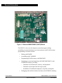

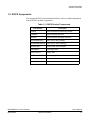
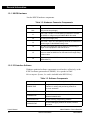
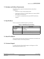

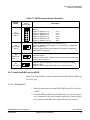
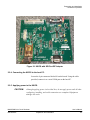
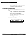
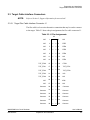
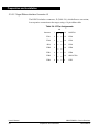
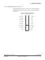
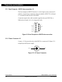
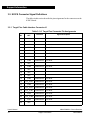
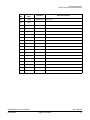
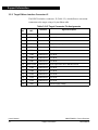
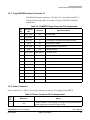
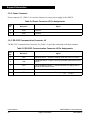
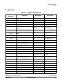
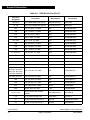
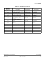
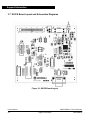
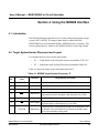
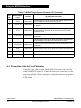
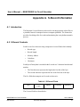
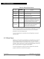
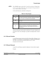
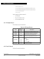
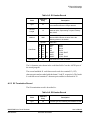
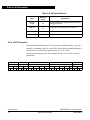
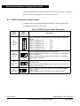

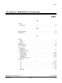
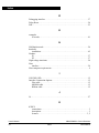
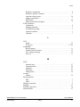
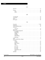







![[DRAFT] DEMO908JL16 User`s Manual](http://vs1.manualzilla.com/store/data/005639706_1-2a84cd2ce2f0b318fdb7aae7896f2a79-150x150.png)