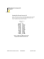
1
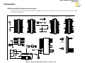
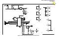
eZ80F91 Modular Development Kit
User Manual
PRELIMINARY
UM017001-0404
ZiLOG Worldwide Headquarters • 532 Race Street • San Jose, CA 95126
Telephone: 408.558.8500 • Fax: 408.558.8300 • www.ZiLOG.com
eZ80F91 Modular Development Kit
User Manual
ii
This publication is subject to replacement by a later edition. To determine whether a later
edition exists, or to request copies of publications, contact:
ZiLOG Worldwide Headquarters
532 Race Street
San Jose, CA 95126
Telephone: 408.558.8500
Fax: 408.558.8300
www.zilog.com
Document Disclaimer
ZiLOG is a registered trademark of ZiLOG Inc. in the United States and in other countries. All other products
and/or service names mentioned herein may be trademarks of the companies with which they are associated.
©2004 by ZiLOG, Inc. All rights reserved. Information in this publication concerning the devices,
applications, or technology described is intended to suggest possible uses and may be superseded. ZiLOG,
INC. DOES NOT ASSUME LIABILITY FOR OR PROVIDE A REPRESENTATION OF ACCURACY OF
THE INFORMATION, DEVICES, OR TECHNOLOGY DESCRIBED IN THIS DOCUMENT. ZiLOG
ALSO DOES NOT ASSUME LIABILITY FOR INTELLECTUAL PROPERTY INFRINGEMENT
RELATED IN ANY MANNER TO USE OF INFORMATION, DEVICES, OR TECHNOLOGY
DESCRIBED HEREIN OR OTHERWISE. Except with the express written approval of ZiLOG, use of
information, devices, or technology as critical components of life support systems is not authorized. No
licenses are conveyed, implicitly or otherwise, by this document under any intellectual property rights.
PRELIMINARY
UM017001-0404
eZ80F91 Modular Development Kit
User Manual
iii
Safeguards
The following precautions must be observed when working with the
devices described in this document.
Caution: Always use a grounding strap to prevent damage resulting from
electrostatic discharge (ESD).
UM017001-0404
PRELIMINARY
Safeguards
eZ80F91 Modular Development Kit
User Manual
iv
PRELIMINARY
UM017001-0404
eZ80F91 Modular Development Kit
User Manual
v
Table of Contents
Safeguards . . . . . . . . . . . . . . . . . . . . . . . . . . . . . . . . . . . . . . . . . . . . . . . . . . . iii
Table of Contents . . . . . . . . . . . . . . . . . . . . . . . . . . . . . . . . . . . . . . . . . . . . . . .v
List of Figures . . . . . . . . . . . . . . . . . . . . . . . . . . . . . . . . . . . . . . . . . . . . . . . vii
List of Tables . . . . . . . . . . . . . . . . . . . . . . . . . . . . . . . . . . . . . . . . . . . . . . . . . ix
Introduction . . . . . . . . . . . . . . . . . . . . . . . . . . . . . . . . . . . . . . . . . . . . . . . . . . .1
Kit Features . . . . . . . . . . . . . . . . . . . . . . . . . . . . . . . . . . . . . . . . . . . . . . . .1
eZ80F91 Modular Development Kit Overview . . . . . . . . . . . . . . . . . . . .3
eZ80Acclaim! MDS Adapter Board . . . . . . . . . . . . . . . . . . . . . . . . . . . . . . . .5
eZ80F91 Mini Enet Module Interface . . . . . . . . . . . . . . . . . . . . . . . . . . .5
eZ80Acclaim! MDS Adapter Board Jumper Settings . . . . . . . . . . . . . .20
eZ80F91 Mini Enet Module. . . . . . . . . . . . . . . . . . . . . . . . . . . . . . . . . . . . . .22
Functional Description . . . . . . . . . . . . . . . . . . . . . . . . . . . . . . . . . . . . . .22
Fast Buffer . . . . . . . . . . . . . . . . . . . . . . . . . . . . . . . . . . . . . . . . . . . .22
Operational Description . . . . . . . . . . . . . . . . . . . . . . . . . . . . . . . . . . . . .24
eZ80F91 Mini Enet Module Memory . . . . . . . . . . . . . . . . . . . . . . .24
External Flash Memory . . . . . . . . . . . . . . . . . . . . . . . . . . . . . . . . . .25
Reset Generator . . . . . . . . . . . . . . . . . . . . . . . . . . . . . . . . . . . . . . . .25
IrDA Transceiver . . . . . . . . . . . . . . . . . . . . . . . . . . . . . . . . . . . . . . .26
Internal On-Chip Flash Memory . . . . . . . . . . . . . . . . . . . . . . . . . . . . . .28
Flash Loader Utility . . . . . . . . . . . . . . . . . . . . . . . . . . . . . . . . . . . . . . . .28
ZDS II. . . . . . . . . . . . . . . . . . . . . . . . . . . . . . . . . . . . . . . . . . . . . . . . . . . . . . .29
Troubleshooting . . . . . . . . . . . . . . . . . . . . . . . . . . . . . . . . . . . . . . . . . . . . . . .31
Overview . . . . . . . . . . . . . . . . . . . . . . . . . . . . . . . . . . . . . . . . . . . . . . . . .31
IrDA Port Not Working . . . . . . . . . . . . . . . . . . . . . . . . . . . . . . . . . . . . .31
Contacting ZiLOG Customer Support . . . . . . . . . . . . . . . . . . . . . . . . . .31
UM017001-0404
PRELIMINARY
Table of Contents
eZ80F91 Modular Development Kit
User Manual
vi
Schematics . . . . . . . . . . . . . . . . . . . . . . . . . . . . . . . . . . . . . . . . . . . . . . . . . .
eZ80Acclaim! MDS Adapter Board Schematic . . . . . . . . . . . . . . .
eZ80F91 Mini Enet Module . . . . . . . . . . . . . . . . . . . . . . . . . . . . . .
Customer Feedback Form . . . . . . . . . . . . . . . . . . . . . . . . . . . . . . . . . . . . . . .
PRELIMINARY
33
33
35
37
UM017001-0404
eZ80F91 Modular Development Kit
User Manual
vii
List of Figures
Figure 1.
Figure 2.
Figure 3.
eZ80Acclaim! MDS Adapter Board Block Diagram . . . . . .3
eZ80F91 Mini Enet Module Block Diagram . . . . . . . . . . . .4
eZ80Acclaim! MDS Adapter Board
Peripheral Bus Mini-Module Connector J1 Pin Configuration
. . . . . . . . . . . . . . . . . . . . . . . . . . . . . . . . . . . . . . . . . . . . . . . .6
Figure 4. eZ80Acclaim! MDS Adapter Board
I/O Mini-Module Connector J2 . . . . . . . . . . . . . . . . . . . . . .10
Figure 5. eZ80Acclaim! MDS Adapter Board
Peripheral Bus External Connector JP1 . . . . . . . . . . . . . . .14
Figure 6. eZ80Acclaim! MDS Adapter Board
I/O External Connector JP2 . . . . . . . . . . . . . . . . . . . . . . . .18
Figure 7. Possible Bus Contention without Fast Buffer . . . . . . . . . . .23
Figure 8. eZ80Acclaim MDS Adapter Board Schematic (1 of 2) . . .33
Figure 9. eZ80Acclaim! MDS Adapter Board Schematic (2 of 2) . . .34
Figure 10. eZ80F91 Mini Enet Module Schematic (1 of 2) . . . . . . . . .35
Figure 11. eZ80F91 Mini Enet Module Schematic (2 of 2) . . . . . . . . .36
UM017001-0404
PRELIMINARY
List of Figures
eZ80F91 Modular Development Kit
User Manual
viii
PRELIMINARY
UM017001-0404
eZ80F91 Modular Development Kit
User Manual
ix
List of Tables
Table 1.
Table 2.
Table 3.
Table 4.
Table 5.
Table 6.
UM017001-0404
eZ80Acclaim! MDS Adapter Board
Peripheral Bus Connector J1 Identification . . . . . . . . . . . . . .7
eZ80Acclaim! MDS Adapter Board
I/O Mini-Module Connector J2 Identification . . . . . . . . . .11
eZ80Acclaim! MDS Adapter Board
Peripheral Bus External Connector JP1 Identification . . . .15
eZ80Acclaim! MDS Adapter Board
I/O External Connector JP21 Identification . . . . . . . . . . . .19
eZ80Acclaim MDS Adapter Board
Jumper Settings . . . . . . . . . . . . . . . . . . . . . . . . . . . . . . . . . .21
Shunt JP1, eZ80F91 Mini Enet Module . . . . . . . . . . . . . . .28
PRELIMINARY
List of Tables
eZ80F91 Modular Development Kit
User Manual
x
PRELIMINARY
UM017001-0404
eZ80F91 Modular Development Kit
User Manual
1
Introduction
The eZ80F91 Modular Development Kit provides a general-purpose platform for creating a design based on ZiLOG’s eZ80F91 microcontroller.
The eZ80F91 is a member of ZiLOG’s eZ80Acclaim!™ product family,
which offers on-chip Flash capability. The eZ80F91 Modular Development Kit features an eZ80F91 Mini Enet Module and an eZ80Acclaim!
MDS Adapter Board onto which the module mounts.
Kit Features
The key features of the eZ80F91 Modular Development Kit are:
•
eZ80F91 Mini Enet Module:
– eZ80F91 device operating at 50 MHz, with 256 KB of internal
Flash memory and 8 KB of internal SRAM memory.
– 128 KB of off-chip SRAM memory.
– On-chip Ethernet Media Access Controller (EMAC).
– Ethernet port and PHY.
– Real-Time Clock with battery backup.
– Footprint for an SIR IrDA transceiver.
– Two 56-pin mini-module connectors for attachment to the
eZ80Acclaim! MDS adapter board.
•
eZ80Acclaim! MDS Adapter Board:
– Footprint for 2M x 8 external Flash memory such as
AM29LV160D.
– Footprint for 10-bit bus switch such as 74CBTLV3384 to support
external Flash.
– RS232 connector with interface circuit for UART0.
– ZDI and JTAG debug connectors.
UM017001-0404
PRELIMINARY
Introduction
eZ80F91 Modular Development Kit
User Manual
2
–
–
–
–
–
–
•
•
•
•
Kit Features
Two 56-pin mini-module connectors.
Two 60-pin interface connectors for connection to an external
application or development board (not supplied).
32-pin header and footprint for a GPRS modem.
One green 3.3 OK LED.
One yellow Test LED and pushbutton.
5VDC external power supply.
Serial Smart Cable
eZ80Acclaim!™ Software and Documentation CD-ROM
ZiLOG ZTP TCP/IP stack CD-ROM
Schematics for the eZ80F91 Mini Enet Module and eZ80Acclaim!
MDS adapter board.
PRELIMINARY
UM017001-0404
eZ80F91 Modular Development Kit
User Manual
3
eZ80F91 Modular Development Kit Overview
The purpose of the eZ80F91 Modular Development Kit is to provide the
design engineer with a set of tools for designing an application based on
the eZ80F91 microcontroller.
A block diagram of the eZ80Acclaim! MDS adapter board is shown in
Figure 1.
ZDI
External 60-pin Headers (two)
External 60-pin Headers (two)
Flash Memory
(not installed)
RS232
Power Supply
Figure 1. eZ80Acclaim! MDS Adapter Board Block Diagram
UM017001-0404
PRELIMINARY
Introduction
eZ80F91 Modular Development Kit
User Manual
4
Figure 2 provides a block diagram of the eZ80F91 Mini Enet Module.
MII
eZ80F91
F91 Bus
Ethernet PHY
EMAC
128KB SRAM
F91 Bus consists of 24 bits of
address, 8 bits of data, 32 bits
of GPIO and control signals.
SIR IrDA
(not installed)
56-Pin Connector J1
56-Pin Connector J2
Figure 2. eZ80F91 Mini Enet Module Block Diagram
Schematics for the eZ80F91 Mini Enet Module and eZ80Acclaim! MDS
adapter board are provided in the Schematics section starting on page 33.
eZ80F91 Modular Development Kit OverviewPRELIMINARY
UM017001-0404
eZ80F91 Modular Development Kit
User Manual
5
eZ80Acclaim! MDS Adapter Board
This section describes functions of the eZ80Acclaim! MDS adapter
board.
eZ80F91 Mini Enet Module Interface
The eZ80F91 Mini Enet Module interface on the eZ80Acclaim! MDS
adapter board consists of two 56-pin mini-module receptacles.
Almost all of these receptacles’ signals are connected directly to the CPU.
Three input signals offer options to the application developer by disabling
certain functions of the eZ80F91 Mini Enet Module.
These three input signals are:
•
Disable IrDA (DIS_IrDA) (used only if you have installed an external
SIR IrDA transceiver onto the eZ80F91 Mini Enet Module)
•
•
F91_WE
RTC_VDD
A description of these three signals follows.
Disable IrDA. When the DIS_IrDA input signal is pulled Low, the IrDA
transceiver located on the eZ80F91 Mini Enet Module is disabled. As a
result, UART0 can be used with the RS232 or the RS485 interfaces on the
eZ80® Development Platform.
F91_WE. When the F91_WE signal is active Low, internal Flash on the
eZ80F91 chip is enabled for writing. This signal is inverted from the
F91_WP signal on the eZ80F91 chip.
RTC_VDD. RTC_VDD is a test point for the Real Time Clock power sup-
ply.
UM017001-0404
PRELIMINARY
eZ80Acclaim! MDS Adapter Board
eZ80F91 Modular Development Kit
User Manual
6
Peripheral Bus Mini-Module Connector, J1
Figure 3 illustrates the pin layout of the 56-pin Peripheral Bus Mini-Module Connector, J1, on the eZ80Acclaim! MDS adapter board. Table 1
identifies the pins and their functions.
Figure 3. eZ80Acclaim! MDS Adapter Board
Peripheral Bus Mini-Module Connector J1 Pin Configuration
eZ80F91 Mini Enet Module Interface
PRELIMINARY
UM017001-0404
eZ80F91 Modular Development Kit
User Manual
7
Table 1. eZ80Acclaim! MDS Adapter Board
Peripheral Bus Connector J1 Identification1,2
Pin #
Symbol
Signal Direction Active Level eZ80F91 Signal
3
A6
Bidirectional
n/a
Yes
4
A0
Bidirectional
n/a
Yes
5
A7
Bidirectional
n/a
Yes
6
A2
Bidirectional
n/a
Yes
7
A8
Bidirectional
n/a
Yes
8
A1
Bidirectional
n/a
Yes
9
A102
Bidirectional
n/a
Yes
10
A3
Bidirectional
n/a
Yes
13
RD
Output
Low
Yes
14
D5
Bidirectional
n/a
Yes
15
D1
Bidirectional
n/a
Yes
16
D4
Bidirectional
n/a
Yes
17
D0
Bidirectional
n/a
Yes
18
D2
Bidirectional
n/a
Yes
19
A17
Bidirectional
n/a
Yes
20
D6
Bidirectional
n/a
Yes
Note
Notes:
1. For the sake of simplicity in describing the interface, Power and Ground nets are omitted from
this table. The entire interface is represented in the eZ80Acclaim! MDS adapter board schematics on pages 33 through 34.
2. Additional note: external capacitive loads on RD, WR, IORQ, MREQ, D0–D7 and A0–A23
should be below 10 pF to satisfy the timing requirements for the eZ80 CPU. All unused inputs
should be pulled to either VDD or GND, depending on their inactive levels to reduce power
consumption and to reduce noise sensitivity. To prevent EMI, the EZ80CLK output can be
deactivated via software in the eZ80F91’s Peripheral Power-Down Register.
UM017001-0404
PRELIMINARY
eZ80Acclaim! MDS Adapter Board
eZ80F91 Modular Development Kit
User Manual
8
Table 1. eZ80Acclaim! MDS Adapter Board
Peripheral Bus Connector J1 Identification1,2 (Continued)
Pin #
Symbol
Signal Direction Active Level eZ80F91 Signal
23
A19
Bidirectional
n/a
Yes
24
A18
Bidirectional
n/a
Yes
25
A21
Bidirectional
n/a
Yes
26
A20
Bidirectional
n/a
Yes
27
A23
Bidirectional
n/a
Yes
28
CS0
Output
Low
Yes
29
CS3
Output
Low
Yes
33
F91_WE
Input
Low
No
34
CS0
Output
Low
Yes
35
D3
Bidirectional
n/a
Yes
36
RTC_VDD
Input
n/a
Yes
39
D7
Bidirectional
n/a
Yes
40
HALT_SLP
Output
Low
Yes
41
A13
Bidirectional
n/a
Yes
42
WR
Ouput
Low
Yes
43
A12
Bidirectional
n/a
Yes
Note
Jumper on board
Notes:
1. For the sake of simplicity in describing the interface, Power and Ground nets are omitted from
this table. The entire interface is represented in the eZ80Acclaim! MDS adapter board schematics on pages 33 through 34.
2. Additional note: external capacitive loads on RD, WR, IORQ, MREQ, D0–D7 and A0–A23
should be below 10 pF to satisfy the timing requirements for the eZ80 CPU. All unused inputs
should be pulled to either VDD or GND, depending on their inactive levels to reduce power
consumption and to reduce noise sensitivity. To prevent EMI, the EZ80CLK output can be
deactivated via software in the eZ80F91’s Peripheral Power-Down Register.
eZ80F91 Mini Enet Module Interface
PRELIMINARY
UM017001-0404
eZ80F91 Modular Development Kit
User Manual
9
Table 1. eZ80Acclaim! MDS Adapter Board
Peripheral Bus Connector J1 Identification1,2 (Continued)
Pin #
Symbol
Signal Direction Active Level eZ80F91 Signal
44
A11
Bidirectional
n/a
Yes
45
A14
Bidirectional
n/a
Yes
46
A9
Bidirectional
n/a
Yes
49
A16
Bidirectional
n/a
Yes
50
A5
Bidirectional
n/a
Yes
51
A15
Bidirectional
n/a
Yes
52
A4
Bidirectional
n/a
Yes
Note
Notes:
1. For the sake of simplicity in describing the interface, Power and Ground nets are omitted from
this table. The entire interface is represented in the eZ80Acclaim! MDS adapter board schematics on pages 33 through 34.
2. Additional note: external capacitive loads on RD, WR, IORQ, MREQ, D0–D7 and A0–A23
should be below 10 pF to satisfy the timing requirements for the eZ80 CPU. All unused inputs
should be pulled to either VDD or GND, depending on their inactive levels to reduce power
consumption and to reduce noise sensitivity. To prevent EMI, the EZ80CLK output can be
deactivated via software in the eZ80F91’s Peripheral Power-Down Register.
UM017001-0404
PRELIMINARY
eZ80Acclaim! MDS Adapter Board
eZ80F91 Modular Development Kit
User Manual
10
I/O Mini-Module Connector, J2
Figure 4 illustrates the pin layout of the 56-pin Peripheral Bus MiniModule Connector, J1, on the eZ80Acclaim! MDS adapter board. Table 2
identifies the pins and their functions.
Figure 4. eZ80Acclaim! MDS Adapter Board
I/O Mini-Module Connector J2
eZ80F91 Mini Enet Module Interface
PRELIMINARY
UM017001-0404
eZ80F91 Modular Development Kit
User Manual
11
Table 2. eZ80Acclaim! MDS Adapter Board
I/O Mini-Module Connector J2 Identification1
Pin #
Symbol
Signal Direction Active Level eZ80F91 Signal2
1
PA3
Bidirectional
n/a
Yes
2
PA4
Bidirectional
n/a
Yes
3
PA7
Bidirectional
n/a
Yes
4
PA5
Bidirectional
n/a
Yes
5
PB5
Bidirectional
n/a
Yes
6
PA0
Bidirectional
n/a
Yes
7
PB6
Bidirectional
n/a
Yes
8
PA1
Bidirectional
n/a
Yes
10
EZ80CLK
Output
n/a
Yes
11
PB1
Bidirectional
n/a
Yes
12
PB7
Bidirectional
n/a
Yes
13
PC4
Bidirectional
n/a
Yes
14
PB3
Bidirectional
n/a
Yes
15
PA6
Bidirectional
n/a
Yes
16
PC7
Bidirectional
n/a
Yes
17
PB4
Bidirectional
n/a
Yes
18
PA2
Bidirectional
n/a
Yes
21
PB3
Bidirectional
n/a
Yes
Notes:
1. For the sake of simplicity in describing the interface, Power and Ground
nets are omitted from this table. The entire interface is represented in the
eZ80Acclaim! MDS adapter board schematics on pages 33 through 34.
2. The Power and Ground nets are connected directly to the eZ80F91 device.
UM017001-0404
PRELIMINARY
eZ80Acclaim! MDS Adapter Board
eZ80F91 Modular Development Kit
User Manual
12
Table 2. eZ80Acclaim! MDS Adapter Board
I/O Mini-Module Connector J2 Identification1
Pin #
Symbol
Signal Direction Active Level eZ80F91 Signal2
22
PB0
Bidirectional
n/a
Yes
23
PC6
Bidirectional
n/a
Yes
24
PC5
Bidirectional
n/a
Yes
25
PC3
Bidirectional
n/a
Yes
26
PC1
Bidirectional
n/a
Yes
27
PC2
Bidirectional
n/a
Yes
28
PC0
Bidirectional
n/a
Yes
31
TMS
Input
n/a
Yes
32
PD7
Bidirectional
n/a
Yes
33
PD6
Bidirectional
n/a
Yes
34
PD5
Bidirectional
n/a
Yes
35
PD3
Bidirectional
n/a
Yes
36
PD4
Bidirectional
n/a
Yes
37
TRSTN
Input
Low
Yes
38
TRIGOUT
Output
n/a
Yes
41
TCK
Input
n/a
Yes
42
PD1
Bidirectional
n/a
Yes
43
TDI
Bidirectional
n/a
Yes
Notes:
1. For the sake of simplicity in describing the interface, Power and Ground
nets are omitted from this table. The entire interface is represented in the
eZ80Acclaim! MDS adapter board schematics on pages 33 through 34.
2. The Power and Ground nets are connected directly to the eZ80F91 device.
eZ80F91 Mini Enet Module Interface
PRELIMINARY
UM017001-0404
eZ80F91 Modular Development Kit
User Manual
13
Table 2. eZ80Acclaim! MDS Adapter Board
I/O Mini-Module Connector J2 Identification1
Pin #
Symbol
Signal Direction Active Level eZ80F91 Signal2
44
PD0
Bidirectional
n/a
Yes
45
PD2
Bidirectional
n/a
Yes
46
TDO
Output
n/a
Yes
49
DIS_IRDA
Input
Low
No
50
IICSCL
I/O
n/a
Yes
51
WAIT
Input
Low
Yes
52
IICSDA
I/O
n/a
Yes
53
RST
I/O
Low
Yes
54
NMI
Input
Low
Yes
Notes:
1. For the sake of simplicity in describing the interface, Power and Ground
nets are omitted from this table. The entire interface is represented in the
eZ80Acclaim! MDS adapter board schematics on pages 33 through 34.
2. The Power and Ground nets are connected directly to the eZ80F91 device.
UM017001-0404
PRELIMINARY
eZ80Acclaim! MDS Adapter Board
eZ80F91 Modular Development Kit
User Manual
14
Peripheral Bus External Connector JP1
Figure 5 illustrates the pin layout of Peripheral Bus External Connector
JP2 in the 60-pin header on the eZ80Acclaim! MDS adapter board.
Table 3 identifies the pins and their functions.
Figure 5. eZ80Acclaim! MDS Adapter Board
Peripheral Bus External Connector JP1
eZ80F91 Mini Enet Module Interface
PRELIMINARY
UM017001-0404
eZ80F91 Modular Development Kit
User Manual
15
Table 3. eZ80Acclaim! MDS Adapter Board
Peripheral Bus External Connector JP1 Identification1
Pin #
Symbol
Signal Direction Active Level eZ80F91 Signal2
1-4, 6, 8, unused
35
n/a
n/a
n/a
5
TRSTN
Input
Low
Yes
11
A6
Bidirectional
n/a
Yes
12
A0
Bidirectional
n/a
Yes
13
A10
Bidirectional
n/a
Yes
14
A3
Bidirectional
n/a
Yes
17
A8
Bidirectional
n/a
Yes
18
A7
Bidirectional
n/a
Yes
19
A13
Bidirectional
n/a
Yes
20
A9
Bidirectional
n/a
Yes
21
A15
Bidirectional
n/a
Yes
22
A14
Bidirectional
n/a
Yes
23
A18
Bidirectional
n/a
Yes
24
A16
Bidirectional
n/a
Yes
25
A19
Bidirectional
n/a
Yes
27
A2
Bidirectional
n/a
Yes
28
A1
Bidirectional
n/a
Yes
Notes:
1. For the sake of simplicity in describing the interface, Power and Ground nets
are omitted from this table. The entire interface is represented in the
eZ80Acclaim! MDS adapter board schematics on pages 33 through 34.
2. The Power and Ground nets are connected directly to the eZ80F91 device.
UM017001-0404
PRELIMINARY
eZ80Acclaim! MDS Adapter Board
eZ80F91 Modular Development Kit
User Manual
16
Table 3. eZ80Acclaim! MDS Adapter Board
Peripheral Bus External Connector JP1 Identification1
Pin #
Symbol
Signal Direction Active Level eZ80F91 Signal2
29
A11
Bidirectional
n/a
Yes
30
A12
Bidirectional
n/a
Yes
31
A4
Bidirectional
n/a
Yes
32
A20
Bidirectional
n/a
Yes
33
A5
Bidirectional
n/a
Yes
34
A17
Bidirectional
n/a
Yes
36
DIS_FLASH Input
Low
No
37
A21
Bidirectional
n/a
Yes
39
A22
Bidirectional
n/a
Yes
40
A23
Bidirectional
n/a
Yes
41
CS0
Output
Low
Yes
42
CS1
Output
Low
Yes
43
CS2
Output
Low
Yes
44-49
D[0:5]
Bidirectional
n/a
Yes
51
D7
Bidirectional
n/a
Yes
52
D6
Bidirectional
n/a
Yes
53
MREQ
Output
Low
Yes
54
IOREQ
Output
Low
Yes
Notes:
1. For the sake of simplicity in describing the interface, Power and Ground nets
are omitted from this table. The entire interface is represented in the
eZ80Acclaim! MDS adapter board schematics on pages 33 through 34.
2. The Power and Ground nets are connected directly to the eZ80F91 device.
eZ80F91 Mini Enet Module Interface
PRELIMINARY
UM017001-0404
eZ80F91 Modular Development Kit
User Manual
17
Table 3. eZ80Acclaim! MDS Adapter Board
Peripheral Bus External Connector JP1 Identification1
Pin #
Symbol
Signal Direction Active Level eZ80F91 Signal2
56
RD
Ouput
Low
Yes
57
WR
Output
Low
Yes
58
INSTRD
Output
Low
Yes
59
BUSACK
Output
Low
Yes
60
BUSREQ
Input
Low
Yes
Notes:
1. For the sake of simplicity in describing the interface, Power and Ground nets
are omitted from this table. The entire interface is represented in the
eZ80Acclaim! MDS adapter board schematics on pages 33 through 34.
2. The Power and Ground nets are connected directly to the eZ80F91 device.
UM017001-0404
PRELIMINARY
eZ80Acclaim! MDS Adapter Board
eZ80F91 Modular Development Kit
User Manual
18
I/O External Connector JP2
Figure 6 illustrates the pin layout of the I/O Connector in the 60-pin
header on the eZ80Acclaim! MDS adapter board. Table 4 identifies the
pins and their functions.
Figure 6. eZ80Acclaim! MDS Adapter Board
I/O External Connector JP2
eZ80F91 Mini Enet Module Interface
PRELIMINARY
UM017001-0404
eZ80F91 Modular Development Kit
User Manual
19
Table 4. eZ80Acclaim! MDS Adapter Board
I/O External Connector JP21 Identification
Signal Direction
eZ80F91 Signal2
Pin #
Symbol
Active Level
1-8
PA7 to PA0 Bidirectional
n/a
Yes
11 - 18
PB7 to PB0 Bidirectional
n/a
Yes
20 - 27
PC7 to PC0 Bidirectional
n/a
Yes
28, 29
PD7, PD6
Bidirectional
n/a
Yes
31 - 36
PD5 to PD0 Bidirectional
n/a
Yes
37
TDO
Output
n/a
Yes
38
TDI
I/O
n/a
Yes
40
TRIGOUT
Output
n/a
Yes
41
TCK
Input
n/a
Yes
42
TMS
Input
n/a
Yes
43
RTC_VDD
Input
n/a
Yes
44
EZ80CLK
Output
n/a
Yes
45
IICSCL
I/O
n/a
Yes
47
IICSDA
I/O
n/a
Yes
49
FLASHWE
Input
Low
No
51
CS3
Output
Low
Yes
52
DIS_IRDA
Input
Low
No
53
RST
I/O
Low
Yes
Notes:
1. For the sake of simplicity in describing the interface, Power and Ground nets are omitted from
this table. The entire interface is represented in the eZ80Acclaim! MDS adapter board schematics on pages 33 through 34.
2. The Power and Ground nets are connected directly to the eZ80F91 device.
UM017001-0404
PRELIMINARY
eZ80Acclaim! MDS Adapter Board
eZ80F91 Modular Development Kit
User Manual
20
Table 4. eZ80Acclaim! MDS Adapter Board
I/O External Connector JP21 Identification (Continued)
eZ80F91 Signal2
Pin #
Symbol
Signal Direction
Active Level
54
WAIT
Input
Low
Yes
57
HALT_SLP
Output
Low
Yes
58
NMI
Input
Low
Yes
60
unused
n/a
n/a
n/a
Notes:
1. For the sake of simplicity in describing the interface, Power and Ground nets are omitted from
this table. The entire interface is represented in the eZ80Acclaim! MDS adapter board schematics on pages 33 through 34.
2. The Power and Ground nets are connected directly to the eZ80F91 device.
eZ80Acclaim! MDS Adapter Board Jumper Settings
The eZ80Acclaim! MDS adapter board contains four jumpers that are
described in Table 5.
eZ80Acclaim! MDS Adapter Board Jumper SettingsPRELIMINARY
UM017001-0404
eZ80F91 Modular Development Kit
User Manual
21
Table 5. eZ80Acclaim MDS Adapter Board
Jumper Settings
Jumper Name
Position
J4, FL_EN
IN (Default) On-board Flash is enabled On-board Flash
(when installed)
J6, FL_WEN1
Affected Device
OUT
On-board Flash is disabled
IN
On-board Flash is disabled On-board Flash
for writing.
(when installed)
OUT
On-board Flash is enabled
for writing
J8, RS232-1 DIS IN
OUT
J9, IRDA_DIS2
Function
RS232 output on connector DB9 connector
P2 is disabled
P2
RS232 output on connector
P2 is enabled
IN (Default) IrDA transceiver on
IrDA transceiver
eZ80F91 Mini Enet Module (when installed)
is disabled
OUT
IrDA transceiver on
eZ80F91 Mini Enet Module
is enabled
Notes:
1. If AM29LV160 is used, J6 and R6 should be OUT. If AT49BV162 is used, R6
should be IN, and J6 should be OUT.
2. Jumper J9 functions only when user has installed IrDA transceiver on eZ80F91
Mini Enet Module.
UM017001-0404
PRELIMINARY
eZ80Acclaim! MDS Adapter Board
eZ80F91 Modular Development Kit
User Manual
22
eZ80F91 Mini Enet Module
This section describes the eZ80F91 Mini Enet Module hardware, its interfaces and key components, including the CPU, real-time clock, and memory.
Functional Description
The eZ80F91 Mini Enet Module is a compact, high-performance module
specially designed for the rapid development and deployment of embedded systems.
Despite its small footprint, the eZ80F91 Mini Enet Module provides a
CPU, Flash memory, Ethernet interface, SRAM, and a real-time clock.
This module is powered by the eZ80F91 microcontroller, a member of
ZILOG’s eZ80Acclaim!™ product family.
Fast Buffer
A Fast Buffer is located on the data bus to Flash memory. The purpose of
this Fast Buffer is to avoid bus contention that can exist due to the slow
turn-off time of Flash memory and the fast bus turn-around time of the
eZ80F91 device (a generic feature of the eZ80Acclaim!™ family when is
used in native mode). The discussion that follows references Figure 7.
Bus contention can occur when two or more devices drive a common bus.
CS0 on the eZ80F91 device drives the Flash CE. Upon accessing Flash
memory, CS0 is driven High a maximum of 8.8 ns after the next rising
edge of the CPU Clock (T6—please refer to the External Memory Read
Timing diagram in the eZ80F91 Product Specification (PS0192) for assistance). The Flash turn-off time (TOD) is 25 ns—the duration from OE or
CE going High to Flash output drivers in a high-impedance state. For further information, see the MT28F008 data sheet on www.micron.com.
eZ80F91 Mini Enet Module
PRELIMINARY
UM017001-0404
eZ80F91 Modular Development Kit
User Manual
23
T6
CPU Clock
T3
CS0
Data In
eZ80F91 Data Bus
Data Out
RD
Bus Contention
TOD
Flash Data Bus
CS1
WR
T4
Figure 7. Possible Bus Contention without Fast Buffer
Essentially, after the eZ80F91 device accesses Flash memory, a time
duration of 8.8 ns + 25 ns = 33.8 ns can transpire before Flash memory
stops driving the data bus. At that time, the eZ80F91 device is well into
the next bus cycle. Assuming this next cycle is the Memory Write cycle,
then the data output of the eZ80F91 device is valid not later than
T3 = 7.5 ns, and the write pulse is asserted not later than 4.5 ns after the
falling edge of the CPU Clock (14.5 ns from the rising edge if the CPU
Clock is 50 MHz). The duration of bus contention, TCON, is 33.8 ns –
7.5 ns = 26.3 ns. Refer to the External Memory Write Timing diagram in
the eZ80F91 Product Specification (PS0192) for assistance.
UM017001-0404
PRELIMINARY
eZ80F91 Mini Enet Module
eZ80F91 Modular Development Kit
User Manual
24
With the addition of a Fast buffer, Flash turn-off time is reduced from
25 ns to 5.5 ns. Bus contention can still occur, but the amount of time it
consumes is not TCON = 26.3 ns but rather TCON = (8.8 ns – 7.5 ns + 5.5 ns)
= 6.8 ns. At this faster rate, data that is being written does not become corrupted because the write pulse is not yet asserted.
As of the date of publication of this document, ZiLOG has not completed
an analysis of the effect that this 6.8 ns period of bus contention has on the
design. An Application Note from Cypress Semiconductor titled NoBL
SRAM and Bus Contention further explains this bus contention issue.
Operational Description
The purpose of the eZ80F91 Mini Enet Module as a feature of the
eZ80F91 Modular Development Kit is to provide application developers
with a design platform that enables them to make use of such eZ80F91
device features of the as on-chip EMAC, SRAM, Flash, etc.
eZ80F91 Mini Enet Module Memory
Static RAM
The eZ80F91 Mini Enet Module features 128 KB of fast SRAM. Access
speed is typically 12 ns, allowing zero-wait-state operation at 50 MHz.
With the CPU at 50 MHz, SRAM can be accessed with zero wait states in
eZ80 mode. CS1_CTL (CS1) can be set to 08h (no wait states).
Note: The eZ80F91 Mini Enet Module is shipped with SRAM powered from
the same power supply as the eZ80F91 device. The SRAM may also be
powered separately by battery. To power SRAM from battery:
1. Remove R15
2. Ensure that R14 is in place.
3. Connect battery (-) to GND.
4. Connect battery (+) to J10.
Operational Description
PRELIMINARY
UM017001-0404
eZ80F91 Modular Development Kit
User Manual
25
Flash Memory
The eZ80F91 Mini Enet Module features 256 KB of on-chip Flash memory, which can be programmed a single byte at a time, or in bursts of up to
256 bytes. Write operations can be performed using either memory or I/O
instructions. Erasing bytes in Flash memory returns them to a value of
FFh. Both the MASS ERASE and PAGE ERASE operations are selftimed by the Flash controller, leaving the CPU free to execute other operations in parallel. Upon power-up, the on-chip Flash memory is located in
the address range 000000h–03FFFFh. Four wait states are programmed
in Flash control register F8h.
On-chip Flash memory is prioritized over all external Chip Selects, can be
enabled or disabled (power-on enabled), and can be programmed within
any 256 KB address space in the 16 MB address range.
The eZ80F91 Mini Enet Module features the following memory configurations:
•
•
•
On-chip SRAM: 8 KB
Off-chip SRAM: 128 KB
On-chip Flash: 256 KB
Refer to the eZ80F91 Product Specification, PS0192, for details on programming internal Flash memory.
External Flash Memory
The eZ80F91 Mini Enet Module provides a footprint for 2MB of external
Flash. The module supports additional external Flash devices via the full
system bus, which is available on the expansion interface connectors.
Reset Generator
A supervisory chip on the eZ80Acclaim! MDS adapter board is connected
to the eZ80F91 Reset input pin via pin 53 of mini-module connector J2..
It performs reliable Power-On Reset functions, generating a reset pulse
UM017001-0404
PRELIMINARY
eZ80F91 Mini Enet Module
eZ80F91 Modular Development Kit
User Manual
26
with a duration of 200 ms if the power supply drops below 2.93 V. This
reset pulse ensures that the board always starts in a defined condition. The
RESET pin on the I/O connector reflects the status of the RESET line. It
is a bidirectional pin for resetting external peripheral components or for
resetting the eZ80F91 Modular Development Kit with a low-impedance
output (e.g. a 100-Ohm push button).
IrDA Transceiver
The eZ80F91 Mini Enet Module is shipped without an IrDA transceiver
installed.
If you install an on-board transceiver, such as the ZiLOG ZHX1810, it is
connected to PD0 (TX), PD1 (RX), and PD2 (Shutdown, IR_SD). The
IrDA transceiver is of the LED type 870 nm Class 1.
The IrDA transceiver is accessible via the IrDA controller attached to
UART0 on the eZ80F91 device.
To use the UART0 as a console or to save power, the transceiver can be
disabled by the software or by an off-board signal when using the proper
jumper selection. The transceiver is disabled by setting PD2 (IRDA_SD)
High or by pulling the DIS_IRDA pin on the I/O connector Low. The
shutdown feature is used for power savings. To enable the IrDA transceiver, DIS_IRDA is left floating and PD2 is pulled Low.
The RxD and TxD signals on the transceiver perform the same functions
as a standard RS232 port. However, these signals are processed as IrDA
3/16 coding pulses (sometimes called IrDA encoder/decoder pulses).
When the IrDA function is enabled, the final output to the RxD and TxD
pins are routed through the 3/16 pulse generator.
Another signal that is used in the eZ80F91 Mini Enet Module’s IrDA system is Shut_Down (SD). The SD pin is connected to PD2 on the eZ80F91
Mini Enet Module. The IrDA control software on the user’s wireless
device must enable this pin to wake the IrDA transceiver. The SD pin
must be set Low to enable the IrDA transceiver. On the eZ80F91 Mini
Enet Module, a two-input OR gate is used to allow an external pin to shut
Operational Description
PRELIMINARY
UM017001-0404
eZ80F91 Modular Development Kit
User Manual
27
down the IrDA transceiver. Both pins must be set Low to enable this function.
The eZ80F91 Mini Enet Module features an Infrared Encoder/Decoder
register that configures the IrDA function. This register is located at
address 0BFh in the internal I/O register map.
The Infrared Encoder/Decoder register contains three control bits. Bit 0
enables or disables the IrDA encoder/decoder block. Bit 1, if it is set,
enables received data to pass into the UART0 Receive FIFO data buffer.
Bit 2 is a test function that provides a loopback sequence from the TxD
pin to the RxD input.
Bit 1, the Receive Enable bit, is used to block data from filling up the
Receive FIFO when the eZ80F91 Mini Enet Module is transmitting data.
Because IrDA signal passes through the air as its transmission medium,
transmitted data can also be received. This Receive Enable bit prevents
this data from being received. After the eZ80F91 Mini Enet Module completes transmitting, this bit is changed to allow for incoming messages.
The code that follows provides an example of how this function is
enabled on the eZ80F91 Mini Enet Module.
//Init_IRDA
// Make sure to first set PD2 as a port bit, an output and set it Low.
PD_ALT1 &= 0xFC;
PD_ALT2 |= 0x03;
UART_LCTL0= 0x80;
BRG_DLRL0=0x2F;
BRG_DLRH0=0x00;
UART_LCTL0=0x00;
UART_FCTL0=0xC7;
UART_LCTL0=0x03;
IR_CTL = 0x03;
UM017001-0404
//
//
//
//
//
//
//
//
//
//
PD0 = uart0tx, PD1 = uart0_rx
Enable alternate function
Select dlab to access baud rate generator
Baud rate Masterclock/(16*baudrate)
High byte of baud rate
Disable dlab
Clear tx fifo, enable fifo
8bit, N, 1 stop
enable IRDA Encode/decode and Receive
enable bit.
PRELIMINARY
eZ80F91 Mini Enet Module
eZ80F91 Modular Development Kit
User Manual
28
//IRDA_Xmit
IR_CTL = 0x01;
Putchar(0xb0);
//Disable receive
//Output a byte to the uart0 port.
Internal On-Chip Flash Memory
To program the 32K boot block on the internal on-chip Flash memory,
shunt JP1 on the eZ80F91 Mini Enet Module must be installed. Table 6
lists the settings shunt JP1.
Table 6. Shunt JP1, eZ80F91 Mini Enet Module
Shunt
Symbol Jumper Name Status
JP1
F91_WE
Function
In (Default) On-chip Flash is enabled for
writing to boot block.
Out
Affected Device
On-chip Flash
On-chip Flash memory boot block On-chip Flash
is write-protected.
Flash Loader Utility
The Flash Loader utility integrated within ZDS II allows the user a convenient way to program on-chip Flash memory. Please refer to the ZiLOG
Developer Studio—eZ80Acclaim! User Manual (UM0144) for more
details.
Internal On-Chip Flash Memory
PRELIMINARY
UM017001-0404
eZ80F91 Modular Development Kit
User Manual
29
ZDS II
ZiLOG Developer Studio II (ZDS II) Integrated Development Environment is a complete stand-alone system that provides a state-of-the-art
development environment. Based on the Windows® Win98SE/NT4.0SP6/Win2000-SP2/WinXP user interfaces, ZDS II integrates a languagesensitive editor, project manager, C-Compiler, assembler, linker, librarian,
and source-level symbolic debugger that supports the eZ80F91 device.
For more information on ZDS II, refer to the ZiLOG Developer Studio—
eZ80Acclaim!™ User Manual, UM0144.
UM017001-0404
PRELIMINARY
ZDS II
eZ80F91 Modular Development Kit
User Manual
30
ZDS II
PRELIMINARY
UM017001-0404
eZ80F91 Modular Development Kit
User Manual
31
Troubleshooting
Overview
Before contacting ZiLOG Customer Support to submit a problem report,
please follow these simple steps. If a hardware failure is suspected, contact a local ZiLOG representative for assistance.
IrDA Port Not Working
If you plan on using the IrDA transceiver on the eZ80F91 Mini Enet
Module, make sure the hardware is set up as follows:
•
Jumper J9 on the eZ80Accaim! MDS adapter board must be OFF (to
enable the control gate that drives the IrDA device)
•
Set port pin PD2 Low. When this port pin and Jumper J9 are turned
OFF, the IrDA device is enabled.
•
Disable the RS232 output by installing a shunt on jumper J8 on the
eZ80Acclaim! MDS adapter board.
Contacting ZiLOG Customer Support
For additional troubleshooting solutions, see ZDS II Online Help.
For valuable information about hardware and software development tools,
visit ZiLOG Customer Support online. Download the latest released version of ZiLOG Developer Studio!
Get the latest software updates from ZiLOG as soon as they are available!
UM017001-0404
PRELIMINARY
Troubleshooting
eZ80F91 Modular Development Kit
User Manual
32
Contacting ZiLOG Customer Support
PRELIMINARY
UM017001-0404
eZ80F91 Modular Development Kit
User Manual
Schematics
33
eZ80Acclaim! MDS Adapter Board Schematic
Figures 8 and 9 provide a schematic for the eZ80Acclaim! MDS adapter board.The SRAM chip U2 and buffer U1 are not installed; they are shown
for reference purposes only.
connector 1
J9
1
2
2
4
6
8
VCC_33V
10
12
14
CR1
16
18
1N5817
20
22
24
26
R2
28
220
30
32
34
RTC_VDD
36
GND
38
-HALT_SLP 40
VL1
-WR
42
A11
44
A9
46
GND
48
A5
50
A4
52
GND
54
VCC_SRAM 56
VCC_33V
A6
A7
A8
A10
GND
-RD
D1
D0
A17
GND
A19
A21
A23
-CS3
VCC_33V
-F91_WE
D3
GND
D7
A13
A12
A14
GND
A16
A15
GND
VCC_SRAM
1
3
5
7
9
11
13
15
17
19
21
23
25
27
29
31
33
35
37
39
41
43
45
47
49
51
53
55
-DIS_IRDA
GND
PA4
2
PA5
4
PA0
6
PA1
8
EZ80CLK
10
PB7
12
PB3
14
PC7
16
PA2
18
GND 20
PB0
22
PC5
24
PC1
26
PC0
28
GND 30
PD7 32
PD5 34
PD4 36
TRIGOUT 38
GND 40
PD1
42
PD0
44
TDO
46
GND 48
IICSCL
50
IICSDA
52
-NMI
54
VCC_33V 56
HEADER 28x2
1
3
5
7
9
11
13
15
17
19
21
23
25
27
29
31
33
35
37
39
41
43
45
47
49
51
53
55
PA3
PA7
PB5
PB6
VCC_33V
PB1
PC4
PA6
PB4
GND
PB2
PC6
PC3
PC2
GND
TMS
PD6
PD3
-TRSTN
GND
TCK
TDI
PD2
GND
-DIS_IRDA
-WAIT
-RST
VCC_33V
1
2
1
3
-TRSTN
5
-F91_WE
7
GND
9
A6
11
A10
13
GND
15
A8
17
A13
19
A15
21
A18
23
A19
25
A2
27
A11
29
A4
31
A5
D1
33
35
LED YEL A21
37
A22
39
-CS0
41
-CS2
43
D1
45
D3
47
D5
49
D7
51
-MREQ 53
GND
55
-WR
57
-BUSACK 59
HEADER 2
DIS IRDA
J10
R14
1
VCC_CUST
VCC_SRAM
0
HEADER 1
R15
VCC_SRAM
VCC_33V
2
VCC_33V
A0
A2
A1
A3
GND
D5
D4
D2
D6
GND
A18
A20
A22
-CS0
VCC_33V
-CS2
connector 2
JP1
J2
0
R1
10K
TEST
R3
PB5
1
J1
330
S1
PB3
1
2
GND
SW PUSHBUTTON
TEST
HEADER 28x2
JP2
2
4
6
8
10
12
14
16
18
20
22
24
26
28
30
32
34
36
38
40
42
44
46
48
50
52
54
56
58
60
PA7
1
PA5
3
PA3
5
PA1
7
VCC_33V 9
PB7 11
PB5 13
PB3
15
PB1
17
GND
19
PC6 21
PC4 23
PC2 25
PC0 27
PD6 29
PD5 31
PD3 33
PD3
PD1 35
PD1 TDO
37
GND
39
TCK
41
RTC_VDD43
IICSCL 45
IICSDA 47
-FLASHWE49
-CS3
51
-RST
53
VCC_33V 55
-HALT_SLP 57
VCC_33V 59
VCC_33V
A0
A3
VCC_33V
A7
A9
A14
A16
GND
A1
A12
A20
A17
-DIS_FLASH
VCC_33V
A23
-CS1
D0
D2
D4
GND
D6
-IOREQ
-RD
-INSTRD
-BUSREQ
HEADER 30x2/SM
2
4
6
8
10
12
14
16
18
20
22
24
26
28
30
32
34
36
38
40
42
44
46
48
50
52
54
56
58
60
PA6
PA4
PA2
PA0
GND
PB6
PB6
PB4
PB2
PB0
PC7
PC5
PC3
PC1
PD7
GND
PD4
PD2
PD2
PD0
PD0
TDI
TRIGOUT
TMS
EZ80CLK
GND
-DIS_IRDA
-WAIT
GND
-NMI
HEADER 30x2/SM
MINI MODULE CONNECTORS
J3
U1
D0
D1
D2
D3
D4
3
4
7
8
11
1A1
1A2
1A3
1A4
1A5
1B1
1B2
1B3
1B4
1B5
2
5
6
9
10
F_D0
F_D1
F_D2
F_D3
F_D4
D5
D6
D7
14
17
18
21
22
2A1
2A2
2A3
2A4
2A5
2B1
2B2
2B3
2B4
2B5
15
16
19
20
23
F_D5
F_D6
F_D7
1
13
1OE
2OE
VCC
GND
24
12
VCC_33V
R4
10K
GND
J4
FLASH_EN
1
2
J12
GND
VCC_33V
C1
0.001uF
GND
74CBTLV3384/SO
HEADER 2
U2
A1
A2
A3
A4
A5
A6
A7
A8
A9
A10
A11
A12
A13
A14
A15
A16
A17
A18
A19
A20
J5
VCC_33V
1
3
5
GND
R5
10K
-CS3
ZDI
INTERFACE
2
4
6
PRSTn
TCK
TDI
Header 3x2
-RST
R6
-RST
VCC_33V
VCC_33V
14
1
14
S2
3
2
1
2 GND
3
R7
VCC_33V
2
7
TC74LVT125
TDI
TDO
TCK
R8
1K
JTAG
TVCC_RESETn
VCC_33V
1
3
5
7
9
11
13
2
4
6
8
10
12
14
F_D0
F_D1
F_D2
F_D3
F_D4
F_D5
F_D6
F_D7
NC
NC
10
13
A21
RY/BY
15
VCC
37
GND
GND
27
46
RESET
VPP
28
OE
FLASH_EN
26
CE
-WR
11
WE
GND
47
BYTE
2
1
HEADER 2
GPRS MODEM
CONNECTORS
A0
J11
24
-RST
GND
VCC_33V
C2
2
1
26
HEADER 9
C3
0.001uF
0.1uF
GND
1
2
3
4
5
6
7
8
9
10
11
12
13
14
15
16
17
18
19
20
21
22
23
24
25
26
27
28
29
30
31
32
GND
GND
VCC_5V
GND
PC4_DTR1
PC6_DCD1
PC3_CTS1
PC5_DSR1
PC7_RI1
PC0_TXD1
PC1_RXD1
PC2_RTS1
PC4
PC6
PC3
PC5
PC7
PC0
PC1
PC2
HEADER 32
Am29LV160D
GND
ZiLOG, Inc.
10K
P1 INTERFACE
GND
GND
D0
D1
D2
D3
D4
D5
D6
D7
D8
D9
D10
D11
D12
D13
D14
D15/A-1
29
31
33
35
38
40
42
44
30
32
34
36
39
41
43
45
1
2
VCC_33V
7
U3A
TC74LVC08
A0
A1
A2
A3
A4
A5
A6
A7
A8
A9
A10
A11
A12
A13
A14
A15
A16
A17
A18
A19
-RD
10K
1
12
14
RESET
U4A
25
24
23
22
21
20
19
18
8
7
6
5
4
3
2
1
48
17
16
9
532 Race Street
San Jose, CA 95126
GND
Title
TMS
PRSTn
eZ80 Acclaim! Platform
J6
HEADER 2
Size
B
Document Number
96C0945-001
Figure 8. eZ80Acclaim MDS Adapter Board Schematic (1 of 2)
UM017001-0404
PRELIMINARY
Schematics
eZ80F91 Modular Development Kit
User Manual
J7
34
F1
VCC_5V
5V
C4
+
PWR JACK
VCC_33V
0.1
C5
22uF
U4B
14
RXE160
VCC_5V
3
1
GND
VIN VOUT
GND
3.3V
2
14
4
U5
VCC_33V
U3B
GND
6
5
TC74LVT125
VCC_33V
5
6
7
+ C6
TC74LVC08
4
R9
LT1086-3.3/TO220
22/6.3
7
680
TC74LVC08
9
8
2
C7
0.1
10
D2
7
GREEN
GND
U3C
TC74LVT125
9
U4D
14
14
10
1
3.3 OK
8
TC74LVC08
12
11
C8
POWER SUPPLY
VCC_33V
U4C
14
2
3
1
13
7
GND
3
V+
GND
7
V-
C1+
MAX3222
2
C1-
4
C2+
5
C2-
6
7
C10
0.1uF
U3D
TC74LVT125
12
C12
0.1uF
U8D
11
8
7
C11
0.1uF
U6
14
13
C9
0.1uF
VCC
19
0.1uF
5
9
4
8
3
7
2
6
1
TxD0
17
T1OUT
T1IN
13
RTS0
8
T2OUT
T2IN
12
RxD0
16
R1IN
R1OUT
15
9
R2IN
R2OUT
10
CTS0
NC
NC
EN
SHDN
PD1
PD3
VCC_33V
U8E
U8A
1
20
2
18
14
11
GND
DB9 FEMALE
9
74LV05
PD0
PD2
14
P2
J8
1
10
1
2
11
74LV05
74LV05
7
GND
RS232-1 DIS
GND
U8C
U8B
4
U8F
74LV05
3
6
5
12
13
GND
PB6
74LV05
74LV05
R10
10K
R11
10K
R12
10K
GND
R13
10K
VCC_33V
ZiLOG, Inc.
Figure 9. eZ80Acclaim! MDS Adapter Board Schematic (2 of 2)
UM017001-0404
PRELIMINARY
Schematics
eZ80F91 Modular Development Kit
User Manual
eZ80F91 Mini Enet Module
Figures 10 through 11 diagram the layout of the eZ80F91 Mini Enet Module. The IrDA device is not installed on the module; it appears for reference purposes only.
connector 1
VCC_33V
connector 2
J1
U1B
GND
J2
-F91_WE
3
-F91_WP
5
-F91_WP
A[0..23]
R2
-CS[0..3]
4.7K
R3
4.7K
IICSDA
IICSCL
IICSDA
IICSCL
IICSDA
IICSCL
-HALT_SLP
-HALT_SLP
RTC_VDD
RTC_VDD
eZ80CLK
eZ80CLK
PA[0..7]
PA[0:7]
PB[0..7]
PB[0:7]
PC[0..7]
PC[0:7]
PD[0..7]
PD[0:7]
-RST
-RST
VCC_33V
-RD
-WR
-RD
-WR
R6
R7
10K
2.2K
2
4
6
8
10
12
14
16
18
20
22
24
26
28
30
32
34
36
38
40
42
44
46
48
50
52
54
56
1
3
5
7
9
11
13
15
17
19
21
23
25
27
29
31
33
35
37
39
41
43
45
47
49
51
53
55
PA4
2
PA5
4
PA0
6
PA1
8
EZ80CLK
10
PB7
12
PB3
14
PC7
16
PA2
18
GND 20
PB0
22
PC5
24
PC1
26
PC0
28
GND 30
PD7 32
PD5 34
PD4 36
TRIGOUT 38
GND 40
PD1
42
PD0
44
TDO
46
GND 48
IICSCL
50
IICSDA
52
-NMI 54
VCC_33V 56
HEADER 28x2
1
3
5
7
9
11
13
15
17
19
21
23
25
27
29
31
33
35
37
39
41
43
45
47
49
51
53
55
PA3
PA7
PB5
PB6
VCC_33V
PB1
PC4
PA6
PB4
GND
PB2
PC6
PC3
PC2
GND
TMS
PD6
PD3
-TRSTN
GND
TCK
TDI
PD2
GND
-DIS_IRDA
-WAIT
-RST
VCC_33V
R1
10K
SN74LVC2G04
HEADER 2
JP1
-F91_WE
VCC_33v
R4
R5
C1
68R
330nF
U2
2R7
(MMA 0204)
5
VCC
1
LEDA
PD0
2
TXD
IRDA_SD
4
SD
PD1
3
RXD
6
GND
T
-CS[0:3]
D[0..7]
VCC_33V
A6
A7
A8
A10
GND
-RD
D1
D0
A17
GND
A19
A21
A23
-CS3
VCC_33V
-F91_WE
D3
GND
D7
A13
A12
A14
GND
A16
A15
GND
VCC_SRAM
ZHX1810
0
D[0:7]
VCC_33V
A0
A2
A1
A3
GND
D5
D4
D2
D6
GND
A18
A20
A22
-CS0
VCC_33V
-CS2
RTC_VDD
GND
-HALT_SLP
-WR
A11
A9
GND
A5
A4
GND
VCC_SRAM
1
2
A[0:23]
HEADER 28x2
-WAIT
-WAIT
-NMI
-NMI
U3
R8
10K
R9
10K
TDI
TCK
TDI
TCK
TRIGOUT
TMS
TDO
-TRSTN
TRIGOUT
TMS
TDO
-TRSTN
A0
A2
A1
A3
A11
A9
A5
A4
A15
A16
A14
A12
A13
A10
A8
A7
A6
1
2
3
4
13
14
15
16
17
18
19
20
21
29
30
31
32
A0
A1
A2
A3
A4
A5
A6
A7
A8
A9
A10
A11
A12
A13
A14
A15
A16
-WR
-RD
-CS1
12
28
5
WE
OE
CS
VCC_33V
I/O0
I/O1
I/O2
I/O3
I/O4
I/O5
I/O6
I/O7
6
7
10
11
22
23
26
27
VCC
VCC
24
8
GND
GND
25
9
U1C
D5
D4
D2
D6
D7
D3
D0
D1
GND
6
2
SN74LVC2G04
VCC_SRAM
C2
0.001uF
C3
0.1uF
VCC_33V
VCC_33V
GND
-DIS_IRDA
1
U1A
7
U4
1
PD2 = IR_SD
SN74LVC2G04
4
IRDA_SD
2
SN74AHC1G32
CONNECTORS
3
4
GND
IDT71V124S/SO
5
8
VCC_33V
VCC_33V
GND
R11
10K
GND
ZiLOG, Inc.
Figure 10. eZ80F91 Mini Enet Module Schematic (1 of 2)
UM017001-0404
PRELIMINARY
Schematics
35
eZ80F91 Modular Development Kit
User Manual
D[0:7]
-BUSREQ
10K
-NMI
TMS
TCK
TDI
-TRSTN
-F91_WP
C11
GND
0.056uF
R18
499
Y2
L6
WAIT
M7
BUSREQ
J6
TMS
TCK
TDI
-TRSTN
H7
L9
K9
L10
TMS
TCK
TDI
TRSTN
K6
RESET
-F91_WP
A2
WP
CRS
COL
RXER
RXDV
RXD3
RXD2
RXD1
RXD0
RXCLK
TXCLK
D8
A7
D6
A4
C4
D5
B4
E6
C5
C6
MII_CRS
MII_COL
MII_RXER
MII_RXDV
MII_RXD3
MII_RXD2
MII_RXD1
MII_RXD0
MII_RXCLK
MII_TXCLK
FILT_IN
XIN
XOUT_O
5MHz
D0
D1
D2
D3
D4
D5
D6
D7
-NMI
-RST
-RST
L2
K3
J4
M3
L3
H5
L4
M4
J10
NMI
FILT_IN
H11
XIN
H12
XOUT
R19
33
C23
C22
18pF
18pF
VCC_33V
RTC_VDD
G7
B5
B12
C2
C8
D9
E3
F9
G3
G6
G12
H4
H6
J12
K8
M2
M11
RTC_VDD
Y3
32.768KHz
C51
22pF
H10
A5
B8
C1
C10
E2
E11
G2
H9
J2
J11
K4
K7
M1
J7
L8
M8
PLL_VDD
VDD
VDD
VDD
VDD
VDD
VDD
VDD
VDD
VDD
VDD
VDD
VDD
VDD
PLL_VSS
VSS
VSS
VSS
VSS
VSS
VSS
VSS
VSS
VSS
VSS
VSS
VSS
VSS
VSS
VSS
VSS
RTC_VDD
RTC_XOUT
RTC_XIN
C52
22pF
GND
eZ80F91_BGA
A0
A1
A2
A3
A4
A5
A6
A7
A8
A9
A10
A11
A12
A13
A14
A15
A16
A17
A18
A19
A20
A21
A22
A23
A1
B1
B2
C3
D4
E5
D2
D1
D3
F6
E1
E4
F1
F2
F3
F4
G1
F5
H1
H2
G4
H3
J1
G5
MII_TXD3
MII_TXD2
MII_TXD1
MII_TXD0
MII_TXEN
MII_TXER
MII_MDC
MII_MDIO
B7
C7
D7
A6
B6
E7
A3
B3
IORQ
MRQ
RD
WR
BUSACK
CS0
CS1
CS2
CS3
M5
L5
K5
J5
L7
J3
K1
K2
L1
SCL
SDA
A11
A12
PA7_PWM3
PA6_PWM2_EC1
PA5_PWM1_TOUT1
PA4_PWM0_TOUT0
PA3_PWM3_OC3
PA2_PWM2_OC2
PA1_PWM1_OC1
PA0_PWM0_OC0
A8
F7
C9
A9
B9
E8
B10
A10
VCC_33V
U5
MDI0
1
MDC
2
RXD3
3
RXD2
4
RXD1
5
RXD0
6
VCC_33V
7
GND 8
RXDV
9
RXCLK
10
RXER
11
GND 12
VDDC
13
TXER
14
TXCLK
15
TXEN
16
TXD0
17
TXD1
18
TXD2
19
TXD3
20
COL
21
CRS
22
GND 23
VCC_33V 24
TXD3
TXD2
TXD1
TXD0
TXEN
TXER
MDC
MDI0
MDIO
MDC
RXD3/PHYAD1
RXD2/PHYAD2
RXD1/PHYAD3
RXD0/PHYAD4
VCC
GND
RXDV/PCS_LPBK
RXC
RXER/ISO
GND
VDDC
TXER
TXC/REFCLK
TXEN
TXD0
TXD1
TXD2
TXD3
COL/RMII
CRS/RMII_BTB
GND
VCC
RST
VDDPLL
XI
XO
GND
GND
VDDTX
TX+
TXGND
VDDRCV
REXT
GND
GND
FXSD/FXEN
RX+
RXVDDRX
PD
LED3/NWAYEN
LED2/DUPLEX
LED1/SPD100/noFEF
LED0/TEST
INT/PHYADD0
-RST
VDD_PLL
48
47
46
45
44
43
42
41
40
39
38
37
36
35
34
33
32
31
30
29
28
27
26
25
25 MHz22pF
GND
GND
GND
C6
TX+
TXGND
R13
6.81K 1%
FB1
GND
GND
C7
0.1uF
C16
0.1uF
+
2
C9
Ferrite Bead
+ C10
0.1uF
10uF
R15 1K
-SPEED
-LEDLNK
R16
C19
47uF
1K
Make sure that power connections
and nets VDD_PLL and VDDC have
the shortest route possible
Header 1
JP2
GND
-RD
-WR
C17
0.1uF
-CS[0:3]
-CS0
-CS1
-CS2
-CS3
1
GND
INT
C15
0.1uF
C8
10uF
RX+
RX-
VDDC
C14
0.1uF
2
Ferrite Bead
+
VDDC
FB2
1
VCC_33V
SCL
SDA
Y1
KS8721BL
C13
0.1uF
-RD
-WR
36
C5 22pF
R26 4.7K
A0
A1
A2
A3
A4
A5
A6
A7
A8
A9
A10
A11
A12
A13
A14
A15
A16
A17
A18
A19
A20
A21
A22
A23
1
-WAIT
-WAIT
R12
VCC_33V
C12
270pF
A[0:23]
U6
D0
D1
D2
D3
D4
D5
D6
D7
C18
0.001uF
C20
47uF
+
VCC_33V
GND
C21
0.1uF
TX+
TX-
IICSCL
IICSDA
RX+
RX-
R20 49.9
PA7
PA6
PA5
PA4
PA3
PA2
PA1
PA0
P1
VCC_33V
R22
49.9
R21 49.9
R23
220
PB7_MOSI
PB6_MISO
PB5_ICB3
PB4_ICA2
PB3_SCK
PB2_SS
PB1_IC1
PB0_IC0_EC0
C11
C12
D10
E9
D11
F8
D12
E10
PB7
PB6
PB5
PB4
PB3
PB2
PB1
PB0
PA[0:7]
E12
G8
F10
F11
F12
G9
G10
G11
PC7
PC6
PC5
PC4
PC3
PC2
PC1
PC0
PB[0:7]
PC7_RI1
PC6_DCD1
PC5_DSR1
PC4_DTR1
PC3_CTS1
PC2_RTS1
PC1_RXD1
PC0_TXD1
H8
K11
K12
J9
K10
L11
L12
M12
PD7
PD6
PD5
PD4
PD3
PD2
PD1
PD0
PC[0:7]
PD7_RI0
PD6_DCD0
PD5_DSR0
PD4_DTR0
PD3_CTS0
PD2_RTS0
PD1_RXD0_IRRXD
PD0_TXD0_IRTXD
HALT_SLP
PHI
INSTRD
TDO
TRIGOUT
M9
B11
M6
M10
J8
VCC_33V
R24
220
R25
49.9
C24
VCC_33V
1
4
2
TX+
TXCT
TX-
3
5
6
RX+
RXCT
RX-
8
GND
9
10
11
12
AN1
CT1
AN2
CT2
0.1uF
-LEDLNK
HFJ11-2450E
-SPEED
C25
0.001uF
C26
0.001uF
C27
0.001uF
C28
0.001uF
C38
0.1uF
C39
0.1uF
C40
0.1uF
C41
0.1uF
C29
0.001uF
C30
0.001uF
C31
0.001uF
C32
0.001uF
C33
0.001uF
GND
VCC_33V
PD[0:7]
-HALT_SLP
eZ80CLK
ZiLOG, Inc.
VCC_33V
VCC_33V
VCC_33V
CPU & PHY
532 Race Street. San Jose,CA 95126. 408.558.8500
Title
TDO
TRIGOUT
GND
eZ80F91 Ethernet Mini Module.
GND
GND
Size
B
Document Number
Rev
Date:
Friday, February 27, 2004
96C0942-001
Sheet
A
2
of
2
Figure 11. eZ80F91 Mini Enet Module Schematic (2 of 2)
UM017001-0404
PRELIMINARY
Schematics
eZ80F91 Modular Development Kit
User Manual
37
Customer Feedback Form
If you note any inaccuracies while reading this User Manual, please copy and complete this form,
then mail or fax it to ZiLOG (see Return Information, below). We also welcome your suggestions!
eZ80F91 Modular Development Kit
Serial # or Board Fab #/Rev. #
Software Version
Document Number
Host Computer Description/Type
Customer Information
Name
Country
Company
Phone
Address
Fax
City/State/Zip
E-Mail
Return Information
ZiLOG
System Test/Customer Support
532 Race Street
San Jose, CA 95126
Phone: (408) 558-8500
Fax: (408) 558-8536
ZiLOG Customer Support
Problem Description or Suggestion
Provide a complete description of the problem or your suggestion. If you are reporting a specific
problem, include all steps leading up to the occurrence of the problem. Attach additional pages as
necessary.
UM017001-0404
PRELIMINARY
Customer Feedback Form