1
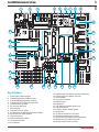
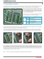
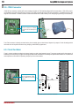
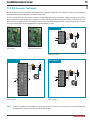
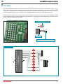
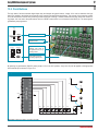
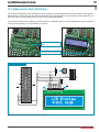
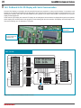
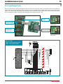
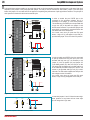
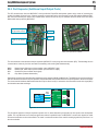
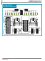
EasyAVR 6
®
Development system
All MikroElektronika´s development systems represent irreplaceable
tools for programming and developing microcontroller-based devices.
Carefully chosen components and the use of machines of the last
generation for mounting and testing thereof are the best guarantee of
high reliability of our devices. Due to simple design, a large number of
add-on modules and ready to use examples, all our users, regardless
of their experience, have the possibility to develop their projects in a
fast and efficient way.
User manual
TO OUR VALUED CUSTOMERS
I want to express my thanks to you for being interested in our products and having confidence in
MikroElektronika.
It is our intention to provide you with the best quality products. Furthermore, we will continue to improve our
performance to better suit your needs.
Nebojsa Matic
General Manager
3
page
EasyAVR6 Development System
TABLE OF CONTENTS
Introduction to EasyAVR6 Development System.............................................................................. 4
Key Features..................................................................................................................................... 5
1.0. Connecting the System to your PC............................................................................................ 6
2.0. Supported Microcontrollers......................................................................................................... 7
3.0. On-Board USB 2.0 AVRprog Programmer................................................................................. 8
4.0. External AVRISP mkII Programmer........................................................................................... 9
5.0 JTAG Connector......................................................................................................................... 10
6.0 Clock Oscillator........................................................................................................................... 10
7.0. Power Supply............................................................................................................................. 11
8.0. RS-232 Communication Interface.............................................................................................. 12
9.0. PS/2 Communication Interface.................................................................................................. 13
10.0. DS1820 Temperature Sensor................................................................................................... 14
11.0. A/D Converter Test Inputs........................................................................................................ 15
12.0. LEDs........................................................................................................................................ 16
13.0. Push Buttons........................................................................................................................... 17
14.0. Keyboards............................................................................................................................... 18
15.0. Alphanumeric 2x16 LCD Display............................................................................................. 19
16.0. On-Board 2x16 LCD Display with Serial Communication........................................................ 20
17.0. 128x64 Graphic LCD Display................................................................................................... 21
18.0. Touch Panel............................................................................................................................. 22
19.0. I/O Ports................................................................................................................................... 23
20.0. Port Expander (Additional I/O Ports)........................................................................................ 25
MikroElektronika
page
4
EasyAVR6 Development System
Introduction to EasyAVR6 Development Board
The EasyAVR6 development system is an extraordinary development tool suitable for programming and experimenting with AVR®
microcontrollers from Atmel®. Such development system includes an on-board programmer providing an interface between the
microcontroller and the PC. You are simply expected to write a code in one of the AVR compilers, generate a HEX file and program your
microcontroller using the AVRprog® programmer. Numerous on-board modules, such as 128x64 graphic LCD display, alphanumeric
2x16 LCD display, on-board 2x16 LCD display with serial communication, keypad 4x4, port expander etc., allow you to easily simulate
the operation of the target device.
AVR
DEVELOPMENT
BOARD
Full-featured and user-friendly
development board for AVR
microcontrollers
High-Performance USB 2.0
On-Board Programmer
Port Expander provides easy
I/O expansion (2 additional
ports) using data format
conversion
Alphanumeric On-Board
2x16 LCD Display with Serial
Communication
Graphic LCD display with
backlight
The AVRflash program provides a complete list of all supported microcontrollers.
The latest version of this program with updated list of supported microcontrollers
can be downloaded from our website www.mikroe.com
Package contains:
Development board:
CD:
Cables:
Documentation:
EasyAVR6
product CD with appropriate software
USB cable
EasyAVR6 and AVRflash manuals, Installing
USB drivers manual and Electrical Schematic
of the EasyAVR6 development system
System specification:
Power supply:
over a DC connector (7V to 23V AC or 9V to 32V DC); or
over a USB cable (5V DC)
Power consumption: 50mA in idle state (when on-board modules are inactive)
Size:
26,5 x 22cm (10,4 x 8,6inch)
Weight:
~417g (0.92lbs)
MikroElektronika
5
1
2
4
3
5
6
7
8
page
EasyAVR6 Development System
9
10
29
11
28
12
27
13
26
14
25
24
23
22
21
20
Key Features
1.
2.
3.
4.
5.
6.
7.
8.
9.
10.
11.
12.
13.
14.
Power supply voltage regulator
On-board programmer’s USB connector
On-boad USB 2.0 programmer AVRprog
External AVRISP® programmer’s connector
JTAG® interface connector
A/D converter test inputs
PS/2 connector
On-board 2x16 LCD display
DIP switches to enable pull-up/pull-down resistors
Pull-up/pull-down mode selection
I/O port connectors
AVR microcontroller sockets
Touch panel controller
Port expander
19
18
15.
16.
17.
18.
19.
20.
21.
22.
23.
24.
25.
26.
27
28.
29.
17
16 15
128x64 graphic LCD display contrast potentiometer
128x64 graphic LCD display connector
Clock oscillator
Touch panel connector
MENU keypad
Keypad 4x4
Push buttons to simulate digital inputs
Logic state selector
Protective resistor ON/OFF jumper
Reset button
35 LEDs to indicate pins’ logic state
DS1820 temperature sensor socket
Alphanumeric LCD display contrast adjustment
Alphanumeric LCD display connector
RS-232 communication connector
MikroElektronika
page
6
EasyAVR6 Development System
1.0. Connecting the System to your PC
Step 1:
Follow the instructions for installing USB drivers and the AVRflash program provided in the relevant manuals. It is not possible to program
AVR microcontrollers without having these devices installed first. In case that you already have some of the MikroElektronika’s compilers
installed on your PC, there is no need to reinstall the AVRflash program as it will be automatically installed along with the compiler.
Step 2:
Use the USB cable to connect the EasyAVR6 development system to your PC. One end of the USB cable provided with a connector of
the USB B type should be connected to the development system as shown in Figure 1-2, whereas the other end of the cable (USB A type)
should be connected to your PC. When establishing a connection, make sure that jumper J6 is placed in the USB position as shown in
Figure 1-1.
DC connector
USB connector
1
2
J6 power supply selector
Figure 1-2: Connecting USB cable (J6 in USB position)
POWER SUPPLY switch
Figure 1-1: Power supply
Step 3:
Turn on your development system by setting the power supply switch to the ON position. Two LEDs marked as ‘POWER’ and ‘USB LINK’
will be turned on to indicate that your development system is ready to use. Use the on-board AVRprog programmer and AVRflash program
to dump a code into the microcontroller and employ the board to test and develop your projects.
NOTE:
If you use some additional modules, such as LCD, GLCD, extra boards etc., it is necessary to place them properly on the development system before it is turned on. Otherwise, they can be permanently damaged. Refer to Figure 1-3 for their proper placing.
Figure 1-3: Placing additional modules on the board
MikroElektronika
7
page
EasyAVR6 Development System
2.0. Supported Microcontrollers
The EasyAVR6 development system provides eight separate sockets for AVR microcontrollers in DIP40, DIP28, DIP20, DIP14 and
DIP8 packages. These sockets allow supported devices in DIP packages to be plugged directly into the development board.
There are two sockets for AVR microcontrollers in DIP40, DIP20
and DIP8 packages provided on the board. Which of these sockets
will you use depends solely on the pinout of the microcontroller
in use. The EasyAVR6 development system comes with the
microcontroller in a DIP40 package.
Jumpers J10 and J11 next to the sockets DIP28 and DIP8 are
used for selecting functions of the microcontroller pins:
Jumper
J10
J11
Position
Function
PB3
PB3 is an I/O pin
OSC
Pin PB3 is fed with a clock signal from
the on-board oscillator
VCC
Pin is connected to VCC
PC7
PC7 is an I/O pin
Figure 2-1: Microcontroller sockets
AVR microcontrollers can use either built-in (internal) or on-board (external) oscillator as a clock signal source. The clock oscillator
provided on the board generates clock signals for most supported microcontrollers.
- Microcontrollers plugged into the DIP8A socket use built-in oscillator for clock generation and are not connected to the on-board oscillator.
- Microcontrollers plugged into the DIP8B socket may use either internal or external oscillator, which depends on the jumper J10 position.
1
3
4
Figure 2-2: Plugging microcontroller into appropriate socket
Prior to plugging the microcontroller into the appropriate socket, make sure that the power supply is turned off. Figure 2-2 shows
how to correctly plug a microcontroller into the appropriate socket. Figure 1 shows an unoccupied DIP40 socket. Place one end of
the microcontroller into the socket as shown in Figure 2. Then put the microcontroller slowly down until all the pins thereof match
the socket as shown in Figure 3. Check again that everything is placed correctly and press the microcontroller easily down until it is
completely plugged into the socket as shown in Figure 4.
NOTE:
Only one microcontroller may be plugged into the development board at the same time.
MikroElektronika
page
8
EasyAVR6 Development System
3.0. On-Board USB 2.0 AVRprog Programmer
The AVRprog programmer is a tool used for dumping .hex code into the microcontroller. The EasyAVR6 has an on-board AVRprog
programmer which allows you to establish a connection between the microcontroller and your PC. Figure 3-2 shows the connection
between a compiler, AVRflash program and microcontroller.
Programmer’s USB connector
Programmer’s chip
Jumper J8 used for selecting programmer
(built-in or external) to be used for
programming AVR chip
Figure 3-1: AVRprog programmer
1 Write a program in some of AVR
compilers and generate a HEX file;
Compiling program
Loading HEX code
1
2
MCU
1110001001 Bin.
0110100011
0111010000
2FC23AA7
1011011001
F43E0021A
Hex. DA67F0541
2 Use the AVRflash program to
select an appropriate microcontroller
and to load the HEX file;
3 Click the Write button to load the
program into the microcontroller.
3
On the right side of the AVRflash
program’s main window there are a
number of buttons which make the
programming process easier. There
is also an option at the bottom of the
window which enables you to monitor
the programming progress.
Write a code in some of AVR compilers, generate
a .hex file and the on-board programmer will take
care of loading data into the microcontroller.
Figure 3-2: The principle of programmer’s operation
NOTE:
For more information on the AVRprog programmer refer to the relevant manual provided in the EasyAVR6 development
system package.
MikroElektronika
AVR microcontrollers are programmed by means of SPI serial communication using the following microcontroller pins MISO, MOSI and SCK.
Build-in programmer AVRprog
Multiplexer
MISO
MOSI
SCK
Programming lines
MISO
MOSI
PROG
CHIP
VCC
DD+
GND
USB
DATA
SCK
User interface
R
R
R
During the programming, a multiplexer disconnects
the microcontroller pins used for programming
from the rest of the board and connects them to
the AVRprog programmer. After the programming
is complete, these pins are disconnected from the
programmer and may be used as input/output
pins.
4.0. External AVRISP mkII Programmer
In addition to the on-board programmer, the EasyAVR6 development system may also use the external AVRISP programmer from
Atmel for programming microcontrollers. Such programmer is plugged into the AVRISP connector.
In order to enable a microcontroller to be programmed using this programmer, it is necessary to set jumper J8 in the EXTERNAL
position prior to turning the programmer on. Then use jumper J7 to select the appropriate microcontroller socket.
Jumper J8 in the EXTERNAL
position enables external
AVRISP programmer
Jumper J8 in the ON-BOARD
position enables on-board
programmer
The position of jumper J7 when the external programmer
is used for programming microcontrollers in DIP20B and
DIP8 packages
The position of jumper J7 when the external programmer
is used for programming microcontrollers in DIP14
package
Figure 4-1: Setting jumper J7
The position of jumper J7 when the external programmer
is used for programming microcontrollers in DIP40 and
DIP20A packages
The position of jumper J7 when the external programmer
is used for programming microcontrollers in DIP28
package
Figure 4-2: AVRISP mkII connected to the development system
MikroElektronika
page
9
EasyAVR6 Development System
page
10
EasyAVR6 Development System
5.0. JTAG Connector
JTAG ICE is an emulator used for AVR microcontrollers with built-in JTAG interface (Mega AVR microcontrollers). JTAG ICE is primarily intended for work with the AVR Studio program. The JTAG connector built into AVR microcontrollers is a modified version of the
original JTAG interface. It enables contents of internal EEPROM and FLASH memory to be changed (programming microcontroller).
JTAG ICE emulator employs a
male 2x5 connector to establish
connection with the development
system
Figure 5-1: JTAG connector
Figure 5-2: JTAGICE mkII connected to the development system
The JTAG connector is directly connected to the microcontroller pins so that it doesn’t depend on jumpers J7 and J8 settings which
otherwise have to be performed when using AVRprog and AVRISP programmers.
6.0. Clock Oscillator
There is a clock oscillator provided on the board used as a clock signal external source. The quartz crystal used for the purpose of
stabilizing clock frequency is plugged into the appropriate socket and therefore can always be replaced with another one. Its maximum
value depends on the maximum operating frequency of the microcontroller.
1M
U9E
74HC04
VCC
U9C
74HC04
EXT CLOCK
X2
8MHz
R65
1K
Figure 6-1: Oscillator
VCC
C34
C35
22pF
22pF
C33
100nF
ATmega16
R64
Quartz crystal X2 plugged
into the appropriate socket,
which enables it to be easily
replaced
PB0
PB1
PB2
PB3
PB4
PB5
PB6
PB7
RESET
VCC
GND
XTAL2
XTAL1
PD0
PD1
PD2
PD3
PD4
PD5
PD6
DIP40
Figure 6-2: Oscillator connection schematic
MikroElektronika
PA0
PA1
PA2
PA3
PA4
PA5
PA6
PA7
AREF
GND
AVCC
PC7
PC6
PC5
PC4
PC3
PC2
PC1
PC0
PD7
VCC
11
page
EasyAVR6 Development System
7.0. Power Supply
The EasyAVR6 development system may use one of two power supply sources:
1. +5V PC power supply through the USB programming cable;
2. External power supply connected to a DC connector provided on the development board.
The MC34063A voltage regulator and Gretz rectifier are used for enabling external power supply voltage to be either AC (in the range
of 7V to 23V) or DC (in the range of 9V to 32V). Jumper J6 is used as a power supply selector. When using USB power supply, jumper
J6 should be placed in the USB position. When using external power supply, jumper J6 should be placed in the EXT position. The
development system is turned on by setting the POWER SUPPLY switch in the ON position.
DC connector
Power supply voltage regulator
USB connector
Jumper J6 as a power
supply selector
POWER SUPPLY switch
Figure 7-1: Power supply
J6
System is powered
through DC connector
EXT
USB
J6
Side view
USB
System is powered through
USB connector
330
35A
8N6
EXT
A
OFF
K
221
SWC
SWE
CT
GND
E1
330uF
D12
D15
C8
VCC
VCC-5V
VCC-USB
LD42
POWER
J6
D7
R56
R55
1K
3K
MBRS140T3
A
K
106
10V
Side view
E2
E3
10uF
330uF
106
10V
Side view
MC
34063A
Bottom view
L2
220uH
DRVC
IPK
Vin
CMPR
MC34063A
220pF
Side view
Top view
U10
D14
AC/DC
CN16
Side view
0.22
4x1N4007
D13
ON
R57
Side view
R14
2K2
+
Side view
Figure 7-2: Power supply source connection schematic
MikroElektronika
page
12
EasyAVR6 Development System
8.0. RS-232 Communication Interface
The USART (universal synchronous/asynchronous receiver/transmitter) is one of the most common ways of exchanging data
between the PC and peripheral components. RS-232 serial communication is performed through a 9-pin SUB-D connector and the
microcontroller USART module. In order to enable such communication, it is necessary to establish a connection between RX and TX
communication lines and microcontroller pins provided with USART module using a DIP switch SW9. The microcontroller pins used in
such communication are marked as follows: RX - receive data and TX - transmit data. Baud rate goes up to 115 kbps.
In order to enable the USART module of the microcontroller to receive input signals with different voltage levels, it is necessary to
provide a voltage level converter such as MAX-202C.
RS-232 connector
Figure 8-1: RS-232 module
The function of DIP switch SW9 is to determine which of the microcontroller pins are to be used as RX and TX lines. The microcontroller
pinout varies depending on the type of the microcontroller. Figure 8-2 shows the connection between the RS-232 module and the
microcontroller in DIP40 package (ATMEGA16).
SW9: RX=PB2, TX=PB3 = ON
SW9
VCC
C28
100nF
C1+
V+
C29
100nF
T1 OUT
C2+
R1 IN
C2-
R1 OUT
T2 OUT
R2 IN
RS232
SUB-D 9p
PB2
PD0
PD2
PB3
PD1
PD3
RX
GND
C1-
V-
C 31
100nF
TX
T1 IN
T2 IN
R2 OUT
VCC
R54
1K
MAX202
VCC
9
5
6
1
Bottom view
1
5
9
6
ATmega16
C30
100nF
VCC
PB0
PB1
PB2
PB3
PB4
PB5
PB6
PB7
RESET
VCC
GND
XTAL2
XTAL1
PD0
PD1
PD2
PD3
PD4
PD5
PD6
PA0
PA1
PA2
PA3
PA4
PA5
PA6
PA7
AREF
GND
AVCC
PC7
PC6
PC5
PC4
PC3
PC2
PC1
PC0
PD7
VCC
DIP40
Figure 8-2: RS-232 module schematic
NOTE:
Make sure that your microcontroller is provided with the USART module as it is not necessarily integrated in all AVR microcontrollers.
MikroElektronika
13
page
EasyAVR6 Development System
9.0. PS/2 Communication Interface
The PS/2 connector enables input units, such as keyboard and mouse, to be connected to the development system. In order to
enable PS/2 communication, it is necessary to correctly place jumpers J16 and J17, thus connecting DATA and CLK lines to the
microcontroller pins PC0 and PC1. Do not connect/disconnect input units to the PS/2 connector while the development system is
turned on as it may permanently damage the microcontroller.
PS/2 connector
Figure 9-1: PS/2 connector
(J16 and J17 are not placed)
Figure 9-2: PS/2 connector
(J16 and J17 are placed)
Jumpers J16 and J17 are placed
VCC
ATmega16
VCC
PB0
PB1
PB2
PB3
PB4
PB5
PB6
PB7
RESET
VCC
GND
XTAL2
XTAL1
PD0
PD1
PD2
PD3
PD4
PD5
PD6
PA0
PA1
PA2
PA3
PA4
PA5
PA6
PA7
AREF
GND
AVCC
PC7
PC6
PC5
PC4
PC3
PC2
PC1
PC0
PD7
R38
1K
R37
1K
PC0 J16
DATA
NC
GND
VCC
CLK
NC
PC1 J17
PS/2
NC
CLK
VCC
DIP40
Figure 9-3: PS/2 connector connection schematic
+5V
NC
DATA
Front view
4 2 1 3
6
5
Bottom view
Figure 9-4: EasyAVR6 connected to keyboard
MikroElektronika
page
14
EasyAVR6 Development System
10.0. DS1820 Temperature Sensor
1-wire® serial communication enables data to be transferred over one single communication line while the process itself is under the
control of the master microcontroller. The advantage of such communication is that only one microcontroller pin is used. All slave devices have by default a unique ID code, which enables the master device to easily identify all devices sharing the same interface.
DS1820 is a temperature sensor that uses 1-wire standard for its operation. It is capable of measuring temperatures within the
range of -55 to 125°C and provides ±0.5°C accuracy for temperatures within the range of -10 to 85°C. Power supply voltage of 3V
to 5.5V is required for its operation. It takes maximum 750ms for the DS1820 to calculate temperature with 9-bit resolution. The
EasyAVR6 development system provides a separate socket for the DS1820. It may use either PA4 or PB2 pin for communication
with the microcontroller. Jumper J9’s purpose is selection of the pin to be used for 1-wire communication. Figure 10-4 shows 1-wire
communication with microcontroller through the PA4 pin.
NOTE: Make sure that half-circle on the
board matches the round side of the
DS1820
Figure 10-1: DS1820
connector (1-wire communication is not used)
Figure 10-2: J11 in the
left-hand position (1-wire
communication through
the PA4 pin)
Figure 10-3: J11 in the
right-hand position (1-wire
communication through
the PB2 pin)
Jumper J9 set in the PA4 position
VCC
R1
1K
DS1820
J9
PA4
DQ
PB2
DS
18
20
VCC
GND
DQ
-55 C
VCC
DQ
Botoom view
VCC GND
ATmega16
125 C
PB0
PB1
PB2
PB3
PB4
PB5
PB6
PB7
RESET
VCC
GND
XTAL2
XTAL1
PD0
PD1
PD2
PD3
PD4
PD5
PD6
DIP40
Figure 10-4: 1-wire communication connection schematic
MikroElektronika
PA0
PA1
PA2
PA3
PA4
PA5
PA6
PA7
AREF
GND
AVCC
PC7
PC6
PC5
PC4
PC3
PC2
PC1
PC0
PD7
VCC
15
page
EasyAVR6 Development System
11.0. A/D Converter Test Inputs
An A/D converter is used for converting an analog signal into the appropriate digital value. A/D converter is linear, which means that the
converted number is linearly dependent on the input voltage value.
The A/D converter within the microcontroller converts an analog voltage value into a 10-bit number. Voltages varying from 0V to 5V DC
may be supplied through the A/D test inputs. Jumper J12 is used for selecting some of the following pins PA0, PA1, PA2, PA3 or PA4. The
R63 resistor has a protective function as it is used for limiting current flow through the potentiometer or the microcontroller pin. The value
of the input analog voltage can be changed linearly using potentiometer P1 (10k).
PA0 is A/D input
VCC
VCC
PB0
PB1
PB3
PB2
PA7
PA6
GND
PA0
PA1
PA2
PA3
PA4
PA5
VCC
J12
R63
P1
10K
DIP14
Figure 11-2: The PA0 pin
used as A/D conversion input
Figure 11-1: ADC (default
jumper positions)
P1
10K
220R
Top view
Figure 11-3: AVR microcontroller in DIP14 package and A/D converter
test inputs connection
PA0 is A/D input
PA0 is A/D input
VCC
J12
ATmega16
VCC
PB0
PB1
PB2
PB3
PB4
PB5
PB6
PB7
RESET
VCC
GND
XTAL2
XTAL1
PD0
PD1
PD2
PD3
PD4
PD5
PD6
PA0
PA1
PA2
PA3
PA4
PA5
PA6
PA7
AREF
GND
AVCC
PC7
PC6
PC5
PC4
PC3
PC2
PC1
PC0
PD7
R63
P1
10K
220R
VCC
J12
P1
10K
VCC
VCC
Top view
PB0
PB1
PB2
PB3
VCC
GND
PB4
PB5
PB6
PB7
PA0
PA1
PA2
PA3
AGND
AVCC
PA4
PA5
PA6
PA7
R63
P1
10K
220R
VCC
P1
10K
Top view
DIP20
DIP40
Figure 11-4: Microcontroller in DIP40 package and A/D converter test
inputs connectiion
NOTE:
Figure 11-5: Microcontroller in DIP20B package and A/D converter test
inputs connection
In order to enable the microcontroller to accurately perform A/D conversion, it is necessary to turn off LED diodes and
pull-up/pull-down resistors on port pins used by the A/D converter.
MikroElektronika
page
16
EasyAVR6 Development System
12.0. LEDs
LED diode (Light-Emitting Diode) is a highly efficient electronic light source. When connecting LEDs, it is necessary to place a current
limiting resistor, the value of which is calculated using formula R=U/I where R is referred to resistance expressed in ohms, U is referred to
voltage on the LED and I stands for LED diode current. A common LED diode voltage is approximately 2.5V, while the current varies from
1mA to 20mA depending on the type of LED diode. The EasyAVR6 development system uses LEDs with current I=1mA.
The EasyAVR6 has 35 LEDs which visually indicate the state of each microcontroller I/O pin. An active LED diode indicates that a logic
one (1) is present on the pin. In order to enable the pin state to be shown, it is necessary to select appropriate port PORTA/E, PORTB,
PORTC or PORTD using the DIP switch SW8.
Notch indicating the SMD LED cathode
A
PA0
PA1
PA2
PA3
PA4
K
I
A
R=U/I
K
SMD LED
472
R
Microcontroller
MCU
SMD resistor limiting current flow through an LED
Figure 12-1: LEDs
SW8: PORTA = ON
ATmega16
VCC
PB0
PB1
PB2
PB3
PB4
PB5
PB6
PB7
RESET
VCC
GND
XTAL2
XTAL1
PD0
PD1
PD2
PD3
PD4
PD5
PD6
PA0
PA1
PA2
PA3
PA4
PA5
PA6
PA7
AREF
GND
AVCC
PC7
PC6
PC5
PC4
PC3
PC2
PC1
PC0
PD7
LD1
PA1
LD2
PA2
LD3
RN13
8x4K7
PA3
LD4
PA4
LD5
PA5
LD6
PA6
LD7
PA7
LD8
SW8
PORTA/E
VCC
DIP40
Figure 12-2: LED diode and PORTA connection schematic
MikroElektronika
PA0
17
page
EasyAVR6 Development System
13.0. Push Buttons
The logic state of all microcontroller digital inputs may be changed using push buttons. Jumper J13 is used to determine the logic
state to be applied to the desired microcontroller pin by pressing the appropriate push button. The purpose of the protective resistor
is to limit the maximum current thus preventing a short circuit from occurring. If needed, advanced users may short such resistor using jumper J18. Just next to the push buttons, there is a RESET button which is not connected to the MCLR pin. The reset signal is
generated by the programmer.
VCC
R20
10K
RSTbut
RESET
RESET button
C32
100nF
Jumper J18 used for shorting
protective resistor
Top view
Inside view
Bottom view
Side view
Jumper J13 used for
selecting logic state to
be applied to the pin by
pressing button
Push buttons used for
simulating digital inputs
Figure 13-1: Push buttons used for simulating digital inputs
By pressing any push button (PA0-PA7) when jumper J13 is in the VCC position, a logic one (5V) will be applied to the appropriate
microcontroller pin as shown in Figure 13-2.
Jumper J13 in the VCC position
ATmega16
VCC
PB0
PB1
PB2
PB3
PB4
PB5
PB6
PB7
RESET
VCC
GND
XTAL2
XTAL1
PD0
PD1
PD2
PD3
PD4
PD5
PD6
PA0
PA1
PA2
PA3
PA4
PA5
PA6
PA7
AREF
GND
AVCC
PC7
PC6
PC5
PC4
PC3
PC2
PC1
PC0
PD7
5V
0V
VCC
J13
VCC
5V
0V
VCC
PA7
PA6
PA5
PA4
PA3
PA2
PA1
J13
PA0
J18
R58
220R
DIP40
Figure 13-2: PORTA push button connection schematic
MikroElektronika
EasyAVR6 Development System
14.0. Keypads
There are two keypads provided on the EasyAVR6 development system. These are keypad 4x4 and keypad MENU. Keypad 4x4 is a
standard alphanumeric keypad connected to the microcontroller PORTC. The performance of such keypad is based on the ‘scan and
sense’ principle where the PC0, PC1, PC2 and PC3 pins are configured as inputs connected to pull-down resistors. The PC4, PC5,
PC6 and PC7 pins are configured as high level voltage outputs. Pressing any button will cause a logic one (1) to be applied to input
pins. Push button detection is performed from within software. For example, pressing button ‘6’ will cause a logic one (1) to appear
on the PC2 pin. In order to determine which of the push buttons is pressed, a logic one (1) is applied to each of the following output
pins PC4, PC5, PC6 and PC7.
Keypad MENU buttons are connected in a similar way to the PORTA buttons. The only difference is in the button arrangement. The
keypad MENU buttons are arranged so as to provide easy navigation through menus.
PC7
PC6
PC5
PC4
PC3
PC2
PC1
PC0
"1"
"1"
"1"
"1"
Pull-down
up
pull
down
RN3
J3
8x10K
J13
SW3
BAT43
A
4
PC7
T38
5
T43
6
T47
T56
T51
T59
T58
T39
8
T44
9
T48
C
T52
*
T40
0
T45
#
T49
D
T53
D10
D11
PC3
PC2
PC1
PC0
Figure 14-4: Keypads (4x4 and MENU) and microcontroller connection schematic
MikroElektronika
B
7
220R
DIP40
T54
T50
T57
220R
R62
A
ENTER
CANCEL
PA5
R61
T46
D9
220R
PC6
3
PA2
R60
T42
T55
220R
PC5
2
PA3
R59
T37
D8
PA0
VCC
PC4
1
J18
Side view
K
PA4
PA0
PA1
PA2
PA3
PA4
PA5
PA6
PA7
AREF
GND
AVCC
PC7
PC6
PC5
PC4
PC3
PC2
PC1
PC0
PD7
PA1
VCC
VCC
VCC
PB0
PB1
PB2
PB3
PB4
PB5
PB6
PB7
RESET
VCC
GND
XTAL2
XTAL1
PD0
PD1
PD2
PD3
PD4
PD5
PD6
ATmega16
Jumper J13 is in
the VCC position.
Pins PC0, PC1,
PC2 and PC3
are connected to
pull-down resistors through DIP
switch SW3
Figure 14-3: Keypad MENU
Figure 14-2: Keypad 4x4 performance
Figure 14-1: Keypad 4x4
PC0
PC1
PC2
PC3
PC4
PC5
PC6
PC7
page
18
R58
220R
19
page
EasyAVR6 Development System
15.0. Alphanumeric 2x16 LCD Display
The EasyAVR6 development system provides an on-board connector so that the alphanumeric 2x16 LCD display can be plugged in.
Such connector is linked to the microcontroller through the PORTD port. Potentiometer P7 is used for display contrast adjustment. The
DISP-BCK switch on the DIP switch SW10 is used for turning on/off display backlight.
Communication between an LCD display and the microcontroller is established using a 4-bit mode. Alphanumeric digits are displayed
in two lines each containing up to 16 characters of 7x5 pixels.
Connector for alphanumeric LCD
display
Contrast adjustment potentiometer
Figure 15-1: Alphanumeric 2x16 LCD display connector
Figure 15-2: 2x16 LCD display
SW10: DISP-BCK = ON
VCC
SW10
P7
10K
PD3
PD2
Top view
PD7
PD6
DISP-BCK
VCC
PD5
PD4
R43
10
GND
VCC
VCC
VO
PD2
GND
PD3
GND
GND
GND
GND
PD4
PD5
PD6
PD7
PA0
PA1
PA2
PA3
PA4
PA5
PA6
PA7
AREF
GND
AVCC
PC7
PC6
PC5
PC4
PC3
PC2
PC1
PC0
PD7
CN7
1
DIP40
GND
VCC
VO
RS
R/W
E
D0
D1
D2
D3
D4
D5
D6
D7
LED+
LED-
ATmega16
VCC
PB0
PB1
PB2
PB3
PB4
PB5
PB6
PB7
RESET
VCC
GND
XTAL2
XTAL1
PD0
PD1
PD2
PD3
PD4
PD5
PD6
LCD Display
4-bit mode
Figure 15-3: Alphanumeric 2x16 LCD display connection schematic
MikroElektronika
EasyAVR6 Development System
16.0. On-Board 2x16 LCD Display with Serial Communication
On-board 2x16 display is connected to the microcontroller through a port expander. In order to use this display, it is necessary to set
switches (1-6) on the DIP switch SW10 to the ON position, thus connecting the on-board LCD display to port expander’s port 1. The
following DIP switches SW6, SW7 and SW9 enable the port expander to use serial communication. Potentiometer P5 is used for
display contrast adjustment.
Unlike common LCD display, the on-board LCD display has no backlight and receives data to be displayed through the port expander
which employs SPI communication for the purpose of communicating with the microcontroller. Such display also shows digits in two
lines each containing up to 16 characters of 7x5 pixels.
Contrast adjustment
potentiometer
DIP switch SW10 to
turn the on-board 2x16
LCD display ON
Figure 16-1: On-board 2x16 LCD display
SW6, SW7: CS, RST, SCK, MISO, MOSI = ON
SW10: 1-6 = ON
SW9
PE-INTA
PE-INTB
PD2
PD3
LCD Display
COG 2x16
P1.3
SW7
VCC
SPI-MOSI
PB5
PB3
PB0
PA6
PB6
PB4
PB1
PA5
P1.5
P1.6
P1.7
VCC
SW6
PB7
PB5
PB2
PA4
PB1
PB3
PB2
PB5
P1.4
CN17
SPI-MISO
VCC
PE-CS#
SPI-SCK
SPI-SCK
PE-CS#
SPI-MOSI
PE-RST#
Top view
Figure 16-2: On-board 2x16 LCD display connection schematic
SPI-MISO
P5
10K
DIP40
MikroElektronika
U5
P1.2
COG-RS
COG-E
COG-D4
COG-D5
COG-D6
COG-D7
DISP-BCK
P01_LED
PA0
PA1
PA2
PA3
PA4
PA5
PA6
PA7
AREF
GND
AVCC
PC7
PC6
PC5
PC4
PC3
PC2
PC1
PC0
PD7
SW10
P1.2
P1.3
P1.4
P1.5
P1.6
P1.7
VCC
ATmega16
VCC
PB0
PB1
PB2
PB3
PB4
PB5
PB6
PB7
RESET
VCC
GND
XTAL2
XTAL1
PD0
PD1
PD2
PD3
PD4
PD5
PD6
GND
Vo
VCC
RS
R/W
E
D0
D1
D2
D3
D4
D5
D6
D7
page
20
R2
100K
GPB0
GPB1
GPB2
GPB3
GPB4
GPB5
GPB6
GPB7
VCC
GND
CS
SCK
SI
SO
GPA7
GPA6
GPA5
GPA4
GPA3
GPA2
GPA1
GPA0
INTA
INTB
RESET
A2
A1
A0
MCP23S17
VCC
PE-INTA
PE-INTB
PE-RST#
21
page
EasyAVR6 Development System
17.0. 128x64 Graphic LCD Display
128x64 graphic LCD display (128x64 GLCD) provides an advanced method for displaying graphic messages. It is connected to the
microcontroller through PORTC and PORTD. GLCD display has the screen resolution of 128x64 pixels which allows you to display
diagrams, tables and other graphic contents. Since the PORTD port is also used by 2x16 alphanumeric LCD display, you cannot use
both displays simultaneously. Potentiometer P6 is used for the GLCD display contrast adjustment. Switch 7 on the DIP switch SW10 is
used for turning on/off display backlight.
Contrast adjustment
potentiometer
GLCD connector
Touch panel connector
Figure 17-2: GLCD connector
Figure 17-1: GLCD display
SW10: DISP-BCK = ON
SW10
P6
10K
Top view
DISP-BCK
VCC
VCC
GND
R28
10
PD2
PD3
GND
VCC
Vo
PD4
PD5
PD6
PC0
PC1
PC2
PC3
PC4
PC5
PC6
PC7
PD7
Vee
PA0
PA1
PA2
PA3
PA4
PA5
PA6
PA7
AREF
GND
AVCC
PC7
PC6
PC5
PC4
PC3
PC2
PC1
PC0
PD7
VCC
CN6
1
CS1
CS2
GND
VCC
Vo
RS
R/W
E
D0
D1
D2
D3
D4
D5
D6
D7
RST
Vee
LED+
LED-
ATmega16
VCC
PB0
PB1
PB2
PB3
PB4
PB5
PB6
PB7
RESET
VCC
GND
XTAL2
XTAL1
PD0
PD1
PD2
PD3
PD4
PD5
PD6
20
DIP40
Figure 17-3: GLCD display connection schematic
MikroElektronika
EasyAVR6 Development System
18.0. Touch Panel
The touch panel is a thin, self-adhesive, transparent panel sensitive to touch. It is placed over a GLCD display. The main purpose
of this panel is to register pressure at some specific display point and to forward its coordinates in the form of analog voltage to the
microcontroller. Switches 5,6,7 and 8 on the DIP switch SW8 are used for connecting touch panel to the microcontroller.
4
3
1
Figure 18-1: Touch panel
Figure 18-1 shows how to place a touch panel over a GLCD display. Make sure that the flat cable is to the left of the GLCD display,
as shown in Figure 4.
1
CS1
CS2
GND
VCC
Vo
RS
R/W
E
D0
D1
D2
D3
D4
D5
D6
D7
RST
Vee
LED+
LED-
VCC-MCU
20
SW8
Q15
BC856
VCC-MCU
R48
1K
R49
1 0K
RIGHT
Q13
BC846
R44
1K
R47
1 0K
BOTTOM
LEFT
DRIVEA
DRIVEB
PA0
PA1
PA2
PA3
Q14
BC856
TOP
R46
1 0K
VCC
RIGHT
TOP
LEFT
BOTTOM
GLCD
C25
100nF
LEFT
SW8: BOTTOM, LEFT, DRIVEA, DRIVEB = ON
Q12
BC846
R52
100K
R45
1 0K
VCC-MCU
BOTTOM
Q16
BC846
R53
100K
R50
1K
R51
1 0K
TOUCHPANEL
CONTROLLER
PB0
PB1
PB2
PB3
PB4
PB5
PB6
PB7
RESET
VCC
GND
XTAL2
XTAL1
PD0
PD1
PD2
PD3
PD4
PD5
PD6
ATmega16
VCC-MCU
CN13
C26
100nF
page
22
PA0
PA1
PA2
PA3
PA4
PA5
PA6
PA7
AREF
GND
AVCC
PC7
PC6
PC5
PC4
PC3
PC2
PC1
PC0
PD7
VCC
DIP40
Figure 18-2: Touch panel connection schematic
1
3
4
Figure 18-3: Placing touch panel
Figure 18-3 shows in detail how to connect a touch panel to the microcontroller. Bring the end of the flat cable close to the CN13 connector as
shown in Figure 1. Plug the cable into the connector, as shown in Figure 2, and press it easily so as to fit the connector, as shown in Figure
3. Now you can plug a GLCD display into the appropriate connector as shown in Figure 4.
NOTE:
LEDs and pull-up/pull-down resistors on the PORTA port must be turned off when using a touch panel.
MikroElektronika
23
page
EasyAVR6 Development System
19.0. Input/Output Ports
Along the right side of the development system, there are seven 10-pin connectors which are connected to the microcontroller’s I/O
ports. Some of the connector pins are directly connected to the microcontroller pins, whereas some of them are connected using
jumpers. DIP switches SW1-SW5 enable each connector pin to be connected to one pull-up/pull-down resistor. Whether port pins are
to be connected to a pull-up or pull-down resistor depends on the position of jumpers J1-J5.
2x5 PORTB male
connector
Jumper for pull-up/pulldown resistor selection
Figure 19-2: J3 in the
pull-down position
DIP switch to turn
on pull-up/pull-down
resistors for each pin
Additional module
connected to PORTC
Figure 19-3: J3 in the
pull-up position
Figure 19-1: I/O ports
SW1: 1-8 = OFF
Jumper J1 in the pull-down position
Jumper J13 in the VCC position
VCC
8x10K
RN1
J1
SW1
PA0
PA1
PA2
PA3
PA4
PA5
PA6
PA7
up
pull
down
ATmega16
VCC
PB0
PB1
PB2
PB3
PB4
PB5
PB6
PB7
RESET
VCC
GND
XTAL2
XTAL1
PD0
PD1
PD2
PD3
PD4
PD5
PD6
PA0
PA1
PA2
PA3
PA4
PA5
PA6
PA7
AREF
GND
AVCC
PC7
PC6
PC5
PC4
PC3
PC2
PC1
PC0
PD7
PA0
LD1
PA1
LD2
PA2
LD3
PA3
LD4
PA4
LD5
PA5
LD6
PA6
LD7
PA7
LD8
RN13
8x4K7
VCC
PORTA
PA0
PA1
PA2
PA3
PA4
PA5
PA7
PA6
CN8
VCC
VCC
DIP40
PA0
PA1
PA2
PA3
PA4
PA5
PA6
J13
PA7
J18
T1
T2
T3
T4
T5
T6
T7
R58
220R
T8
Figure 19-4: PORTA connection schematic
MikroElektronika
page
24
EasyAVR6 Development System
Pull-up/pull-down resistors enable you to set the logic level on all microcontroller input pins when they are in idle state. Such level
depends on the position of the pull-up/pull-down jumper. The PA0 pin with the relevant DIP switch SW1, jumper J1 and PA0 push
button with jumper J13 are used here for the purpose of explaining the performance of pull-up/pull-down resistors. The principle of
their operation is identical for all the microcontroller pins.
VCC
ATmega16
VCC
PB0
PB1
PB2
PB3
PB4
PB5
PB6
PB7
RESET
VCC
GND
XTAL2
XTAL1
PD0
PD1
PD2
PD3
PD4
PD5
PD6
PA0
PA1
PA2
PA3
PA4
PA5
PA6
PA7
AREF
GND
AVCC
PC7
PC6
PC5
PC4
PC3
PC2
PC1
PC0
PD7
up
pull
down
8x10K
RN1
J1
SW1
VCC
J13
PA0
J18
R58
220R
VCC
In order to enable the port PORTA pins to be
connected to the pull-down resistors, first it is
necessary to set jumper J1 in the Down position.
This enables any port PORTA pin to be provided with
a logic zero (0V) in idle state over jumper J1 and
8x10K resistor network. To provide the PA0 pin with
such signal, it is necessary to set switch PA0 on the
DIP switch SW1 in the ON position.
As a result, every time you press the PA0 push
button, a logic one (1) will appear on the PA0 pin,
provided that jumper J13 is set in the VCC position.
5V
0V
DIP40
Figure 19-5: Jumper J1 in pull-down and J13 in pull-up position
VCC
ATmega16
VCC
PB0
PB1
PB2
PB3
PB4
PB5
PB6
PB7
RESET
VCC
GND
XTAL2
XTAL1
PD0
PD1
PD2
PD3
PD4
PD5
PD6
PA0
PA1
PA2
PA3
PA4
PA5
PA6
PA7
AREF
GND
AVCC
PC7
PC6
PC5
PC4
PC3
PC2
PC1
PC0
PD7
up
pull
down
RN1
J1
8x10K
SW1
VCC
J13
PA0
J18
VCC
R58
220R
In order to enable port PORTA pins to be connected
to pull-up resistors and the port input pins to be
acivated with logic zero (0), it is necessary to set
jumper J1 in the Up position (5V) and jumper J13
in the GND position (0V). Also, the PA0 pin on the
DIP switch SW1 should be set in the ON position so
as to enable all port PORTA input pins, over the 10k
resistor, to be provided with logic one (5V) in their
idle state. The PA0 switch supplies the PA0 pin with
this voltage over the 10k resistor.
As a result, every time you press the PA0 push
button, a logic zero (0) will appear on the PA0 pin.
5V
0V
DIP40
Figure 19-6: Jumper J1 in pull-up and J13 in pull-down position
VCC
up
pull
down
J1
VCC
J13
5V
0V
Figure 19-7: Jumpers J1 and J13 in the same position
MikroElektronika
In case that jumpers J1 and J13 have the same logic
state, pressure on any button will not cause input
pins to change their logic state.
25
page
EasyAVR6 Development System
20.0. Port Expander (Additional Input/Output Ports)
The SPI communication lines and MCP23S17 circuit provide the EasyAVR6 development system with a means of increasing the
number of available I/O ports by two. If the port expander communicates to the microcontroller over the DIP switches SW6 and SW7,
then the microcontroller pins used for SPI communication cannot be used as I/O pins. Switches INTA and INTB on the DIP switch
SW9 enable interrupt used by MCP23S17.
Jumper for selecting
pull-up/pull-down resistor
PORT0
PORT1
DIP switch connecting port
expander to the microcontroller
Figure 20-2: DIP switches SW6 and SW7
when port expander is enabled
Figure 20-1: Port expander
The microcontroller communicates to the port expander (MCP23S17 circuit) using serial communicaion (SPI). The advantage of such
communication is that only four lines are used for transmitting and receiving data simultaneously:
MOSI
MISO
SCK
CS
- Master Output, Slave Input (microcontroller output, MCP23S17 input)
- Master Input, Slave Output (microcontroller input, MCP23S17 output)
- Serial Clock (microcontroller clock signal)
- Chip Select (enables data transfer)
Data transfer is performed in both directions simultaneously by means of MOSI and MISO lines. The MOSI line is used for transferring
data from the microcontroller to the port expander, whereas the MISO line transfers data from the port expander to the microcontroller.
The microcontroller initializes data transfer when the CS pin is driven low (0V). It causes the microcontroller to send clock signal (SCK)
and therefore starts data exchange.
SPI
Master
AVR MCU
MOSI
Serial
output
PORT
EXPANDER
MOSI
MISO
MISO
SCK
SCK
CS
Parallel
input
8bit
PORT0
8bit
PORT1
CS
SPI Slave
MCP23S17
Figure 20-3: SPI communication block diagram
The principle of operation of the port expander’s ports 0 and 1 is almost identical to the operation of other ports on the development
system. The only difference here is that port signals are received in parallel format. The MCP23S17 converts such signals into serial
format and sends them to the microcontroller. The result is a reduced number of lines used for sending signals from ports 0 and 1 to
the microcontroller.
MikroElektronika
EasyAVR6 Development System
SW6: CS#=PB1, RST=PB2, SCK = PB7
SW7: PB6 =MISO, PB5=MOSI
Jumpers J14 and J15 in the pull-up position
8x2K2
LD60
LD59
LD58
LD57
LD56
LD55
LD54
LD53
P1.7
P1.6
P1.5
P1.4
P1.3
P1.2
P1.1
P1.0
VCC
ATmega16
VCC
PB0
PB1
PB2
PB3
PB4
PB5
PB6
PB7
RESET
VCC
GND
XTAL2
XTAL1
PD0
PD1
PD2
PD3
PD4
PD5
PD6
PA0
PA1
PA2
PA3
PA4
PA5
PA6
PA7
AREF
GND
AVCC
PC7
PC6
PC5
PC4
PC3
PC2
PC1
PC0
PD7
P1.0
P1.2
P1.4
P1.6
J15
up
pull
down
PORT1
P1.1
P1.3
P1.5
P1.7
CN14
P1.1
VCC
P1.0
P1.1
P1.2
P1.3
P1.4
P1.5
P1.6
P1.7
VCC
8x10K
P1.3
P1.4
P1.5
P1.6
P1.7
CS#
SW6
Figure 20-3: Port expander connection schematic
P1.2
VCC
SPI-SCK
SCK
MOSI
PE-CS#
LD52
LD51
LD50
LD49
LD48
LD47
LD46
LD45
P0.7
P0.6
P0.5
P0.4
P0.3
P0.2
P0.1
P0.0
P0.0
P0.2
P0.4
P0.6
U5
RN7
PB7
PB5
PB2
PA4
PB1
PB3
PB2
PB5
8x2K2
RN12
P1.0
DIP40
MikroElektronika
SW10
RN11
P01_LED
page
26
R2
100K
MISO
GPB0
GPB1
GPB2
GPB3
GPB4
GPB5
GPB6
GPB7
VCC
GND
CS
SCK
SI
SO
MCP23S17
PE-RST#
VCC
GPA7
GPA6
GPA5
GPA4
GPA3
GPA2
GPA1
GPA0
INTA
INTB
RESET
GND
GND
GND
PORT0
VCC
P0.1
P0.3
P0.5
P0.7
J14
up
pull
down
P0.7
CN15
P0.6
P0.5
P0.4
P0.3
P0.2
P0.1
P0.0
VCC
RN6
P0.0
P0.1
P0.2
P0.3
P0.4
P0.5
P0.6
P0.7
8x10K
INTA
INTB
RST
SW9
PE-INTA
PE-INTB
SW7
PD2
PD3
PB5
PB3
PB0
PA6
PB6
PB4
PB1
PA5
SPI-MOSI
SPI-MISO
TÉRMINOS Y CONDICIONES
Todos los productos de MikroElektronika son protegidos por la ley y por los tratados internacionales de
derechos de autor. Este manual es protegido por los tratados de derechos de autor, también. Es prohibido
copiar este manual, en parte o en conjunto sin la autorización previa por escrito de MikroElektronika. Se
permite imprimir este manual en el formato PDF para el uso privado. La distribución y la modificación de
su contenido son prohibidas.
MikroElektronika proporciona este manual “como está” sin garantías de ninguna especie, sean expresas
o implícitas, incluyendo las garantías o condiciones implícitas de comerciabilidad y aptitud para fines
específicos.
Aunque MikroElektronika ha puesto el máximo empeño en asegurar la exactitud de la información incluida
en este manual, no asume la responsabilidad de ninguna especie de daños derivados del acceso a la
información o de los programas y productos presentados en este manual (incluyendo daños por la pérdida
de los beneficios empresariales, información comercial, interrupción de negocio o cualquier otra pérdida
pecuniaria).Las informaciones contenidas en este manual son para el uso interno. Pueden ser modificadas
en cualquier momento y sin aviso previo.
ACTIVIDADES DE ALTO RIESGO
Los productos de MikroElektronika no son tolerantes a fallos y no están diseñados, fabricados o pensados
para su uso o reventa como equipo de control en línea en entornos peligrosos que requieran un funcionamiento sin fallos, como en instalaciones nucleares, en la navegación aérea o en sistemas de comunicaciones, de tráfico aéreo, máquinas de auxilio vital o sistemas de armamento, en los que un fallo del software
podría conducir directamente a la muerte, lesiones corporales o daños físicos o medioambientales graves
(“Actividades de alto riesgo”). MikroElektronika y sus proveedores niegan específicamente cualquier garantía expresa o implícita de aptitud para Actividades de alto riesgo.
MARCAS REGISTRADAS
Los productos y los nombres corporativos utilizados en este manual son protegidos por la ley de los
derechos de autor, sin reparar en la ausencia de notas adicionales. Las marcas registradas son utilizadas
exlusivamente con el propósito de identificar y explicar los conceptos correspondientes y en beneficio de
sus respectivos propietarios, sin intención de infringirlas.
Copyright© 2003 – 2009 por MikroElektronika. Todos los derechos reservados.
Si tiene alguna pregunta, comentario o propuesta de negocio, póngase en contacto con nosotros en [email protected]
Si tiene problemas con cualquiera de nuestros productos o sólo necesita información adicional,
deje un ticket en www.mikroe.com/en/support
Si quiere saber más de nuestros productos, por favor visite nuestra página web www.mikroe.com