1
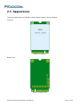
H380 M.2 Series Module Hardware User Manual Version:V1.0.6 Date:2015.08.19 Copyright Copyright ©2015 Fibocom Wireless Inc . All rights reserved. Without the prior written permission of the copyright holder, any company or individual is prohibited to excerpt, copy any part of or the entire document, or transmit the document in any form. Attention The document is subject to update from time to time owing to the product version upgrade or other reasons. Unless otherwise specified, the document only serves as the user guide. All the statements, information and suggestions contained in the document do not constitute any explicit or implicit guarantee. Trademark The trademark is registered and owned by Fibocom Wireless Inc. Versions Version Date Remarks V1.0.0 2014-03-20 Initial Version. 1, Update the reference value of the current part. V1.0.1 2014-04-18 2, Update the GPS function. 3, Update the temperature. V1.0.2 2014-06-20 Add the supported description of Win8/Android dual-system switched. V1.0.3 2015-02-26 Add the new types. V1.0.4 2015-04-21 Add the top view in PCB Layout part. 部 V1.0.5 2015-05-20 V1.0.6 2015-08-19 1. Update the description of copyright and attention. 2. Update the translation of all the whole document . Update the logo. H380 M.2 Series Module Hardware User Manual Page 2 of 42 Applicability Type No. Type Note 1 H380-Q50-00 2 H380-A50-00 3 H380-B50-00 The difference of H380 M.2 series wireless module as listed below: Model No. GSM/GPRS/EDGE Band(MHz) WCDMA Band(MHz) HSDPA HSUPA (Mbps) (Mbps) H380-Q50-00 850&900&1800&1900 850&900&1900&2100 21 5.76 H380-A50-00 900&1800 900&2100 21 5.76 H380-B50-00 850&1900 850&1900 21 5.76 H380 M.2 Series Module Hardware User Manual Page 3 of 42 Content 1 Foreword.................................................................................................................................................................... 7 1.1 Introduction.....................................................................................................................................................7 1.2 Reference Standard......................................................................................................................................7 2 Product Overview..................................................................................................................................................... 9 2.1 Description......................................................................................................................................................9 2.2 Specification................................................................................................................................................... 9 2.3 Appearance..................................................................................................................................................11 3 Structure...................................................................................................................................................................12 3.1 Dimension Diagram of Structure.............................................................................................................. 12 3.2 Application Interface Description..............................................................................................................13 3.3 M.2 Connector............................................................................................................................................. 14 4 Hardware Introduction........................................................................................................................................... 15 4.1 Hardware Diagram......................................................................................................................................15 4.2 Pin Definitions..............................................................................................................................................16 4.2.1 Pin Map............................................................................................................................................. 16 4.2.2 Description of Pins...........................................................................................................................17 5 Hardware Interface.................................................................................................................................................21 5.1 Power Interface........................................................................................................................................... 21 5.1.1 Power Supply................................................................................................................................... 21 5.1.2 Consumption.................................................................................................................................... 21 5.2 Power on/off and Reset Signal................................................................................................................. 25 5.2.1 Pins Definition of Power on/off Control Signal............................................................................25 5.2.2 Power on /off Signal........................................................................................................................ 25 5.2.3 RESET Signal.................................................................................................................................. 26 5.3 Status Indicating Signal............................................................................................................................. 27 5.3.1 Status Indicating Pin....................................................................................................................... 27 5.4 USB Interface...............................................................................................................................................27 5.4.1 USB Interface Definition................................................................................................................. 27 5.4.2 USB Interface Application.............................................................................................................. 28 5.5 USIM Interface.............................................................................................................................................28 5.5.1 USIM Pins......................................................................................................................................... 28 5.5.2 USIM Interface Design....................................................................................................................29 H380 M.2 Series Module Hardware User Manual Page 4 of 42 5.5.2.1 “Normal Closed”SIM Card Circuit Design........................................................................ 29 5.5.2.2 “Normally Open” SIM Circuit Design.................................................................................29 5.5.3 Points for Attention in USIM Design............................................................................................. 30 5.5.4 USIM Hot-Plugging..........................................................................................................................30 5.5.4.1 Hardware Connection..........................................................................................................30 5.5.4.2 Software Settings................................................................................................................. 31 5.6 Digital Audio................................................................................................................................................. 31 5.6.1 I2S...................................................................................................................................................... 32 5.6.2 I2C...................................................................................................................................................... 32 5.6.3 PCM Port Description..................................................................................................................... 32 5.7 Win8/Android Switch Control Interface................................................................................................... 33 5.8 W_DISABLE# Interface............................................................................................................................. 33 5.8.1 Description of WWAN_DISABLE# Interface...............................................................................33 5.8.2 GPS_DISABLE# Interface............................................................................................................. 34 5.9 TX_BLANKING Interface........................................................................................................................... 34 5.10 WAKEUP Host Interface..........................................................................................................................35 5.11 BODY_SAR Interface...............................................................................................................................35 5.12 Clock Interface.......................................................................................................................................... 35 5.13 Config Interface.........................................................................................................................................35 5.14 RF Interface............................................................................................................................................... 37 5.14.1 RF Connector Interface................................................................................................................ 37 5.14.2 RF Connecting Seat......................................................................................................................37 5.14.3 Main Performance of RF Connector.......................................................................................... 38 5.15 Other Interfaces........................................................................................................................................ 38 6 Electrical and Environmental Features...............................................................................................................39 6.1 Electrical Features...................................................................................................................................... 39 6.2 Environmental Features.............................................................................................................................39 7 RF Interface.............................................................................................................................................................40 7.1 Operating Frequency Band....................................................................................................................... 40 7.1.1 Diversity Antenna Band.................................................................................................................. 40 7.2 RF PCB Design........................................................................................................................................... 41 7.2.1 Impedance Design...........................................................................................................................41 7.3 Antenna Design........................................................................................................................................... 41 7.3.1 Main Antenna Design Requirements........................................................................................... 41 H380 M.2 Series Module Hardware User Manual Page 5 of 42 7.3.2 Diversity Antenna Design...............................................................................................................42 H380 M.2 Series Module Hardware User Manual Page 6 of 42 1 Foreword 1.1 Introduction The document describes the electrical characteristics, RF performance, dimensions and application environment, etc. of H380 M.2 series wireless communication modules. With the assistance of the document and other instructions, developers can quickly understand the performance of H380 M.2 series wireless communication modules and develop products. 1.2 Reference Standard The design of the product compiles with the following standards : • 3GPP TS 27.007 -v6.9.0: AT command set for User Equipment (UE) • 3GPP TS 27.005 -v6.0.1: Use of Data Terminal Equipment -Data Circuit terminating Equipment (DTE-DCE) interface for Short Message Service (SMS) and Cell Broadcast Service (CBS) • 3GPP TS 23.040 -v6.9.0: Technical realization of Short Message Service (SMS) • 3GPP TS 24.011 -v6.1.0: Point- to - Point (PP) Short Message Service (SMS) support on mobile radio interface • 3GPP TS 27.010 -v6.0.0: Terminal Equipment to User Equipment (TE-UE) multiplexer protocol • 3GPP TS • 3GPP TS 25.304-v6.10.0: User Equipment (UE) procedures in idle mode and procedures for cell re 27.060 -v6.0.0: Packet domain; Mobile Station (MS) supporting Packet Switched services selection in connected mode • 3GPP TS 25.308 -v6.4.0: High Speed Downlink Packet Access (HSDPA); Overall description;Stage 2 • 3GPP TS 25.309 -v6.6.0: FDD enhanced uplink; Overall description; Stage 2 • 3GPP TS 23.038 -v6.1.0: Alphabets and language - specific information • 3GPP TS 21.111 -v6.3.0: USIM and IC card requirements • 3GPP TS 31.111 -v6.11.0 "USIM Application Toolkit (USAT)" • 3GPP TS 45.002 -v6.12.0: Multiplexing and • 3GPP TS 51.014 -v4.5.0: Specification of the SIM Application Toolkit for the Subscriber Identity multiple access on the radio path Module - Mobile Equipment (SIM-ME) interface • 3GPP TS 51.010 -1 -v6.7.0: Mobile Station (MS) conformance specification; Part 1: Conformance specification • 3GPP TS 22.004 -v6.0.0: General on supplementary services • 3GPP TS 23.090 -v6.1.0: Unstructured Supplementary Service Data (USSD); Stage 2 H380 M.2 Series Module Hardware User Manual Page 7 of 42 • 3GPP TS 24.008 v6.19, Mobile radio interface Layer 3 specification; • PCIe_M.2_Electromechanical_Spec_Rev0.9-3_07312013_RS_Clean[1] H380 M.2 Series Module Hardware User Manual Page 8 of 42 2 Product Overview 2.1 Description H380 M.2 series are highly integrated 3G wireless modules, supports GSM/GPRS/EDGE and UMTS/ HSDPA / HSUPA/HSPA+,GPS/GNSS(supported in future). 2.2 Specification Specification Operating UMTS (WCDMA): 850/900/1900/2100MHz Frequency Range GSM/GPRS/EDGE: 850/900/1800/1900MHz UMTS/HSDPA/HSUPA 3GPP release 7 HSUPA 5.76Mbps (Cat 6) HSDPA 21Mbps (Cat 14) 或 7.2Mbps (Cat 8) Data Rare GSM 3GPP release 7 EDGE (E-GPRS) multi-slot class 33(296kbps DL,236.8kbps UL) GPRS multi-slot class 33(107kbps DL,85.6kbps UL) GPS GPS/GNSS(supported in future) Dimension:42mm x 22mm x 2.35 mm Physical Characteristics Environment Interface:M.2 Weight:5.0 grams Operating Temperature:-30℃ ~ +75℃ Storage Temperature:-40℃ ~ +85℃ Performance Operating Voltage Voltage:3.135V ~ 4.4V Normal:3.3V Current 3mA (Sleep Mode) Consumption 3G Talk:660mA (Typical Value) 2G Talk:270mA (GSM PCL5) Class 4 (2W): 850/900 MHz, GSM Rx Power (Typical Value) Class 1 (1W):1800/1900 MHz, GSM Class E2 (0.5W): 850/900 MHz, EDGE H380 M.2 Series Module Hardware User Manual Page 9 of 42 Class E2 (0.4W):1800/1900 MHz, EDGE Class 3 (0.25W): 900/850/1900/2100 MHz, WCDMA Tx Sensitivity UMTS/HSPA:-109dBm (Typical Value) GSM:-108dBm Interfaces RF Interface Antenna:Mainx1,Diversityx1(RF diversity and GPS Aux) 1 x USB 2.0,Multiple Profiles over USB Function Interface I2C Support,I2S/PCM Support GPIO Data Features Protocol Stack Embedded TCP/IP and UDP/IP protocol stack Multi-slot class 33 (5 Down; 4 Up; 6 Total) EDGE Coding Scheme MCS1~9 Multi-slot class 33 (5 Down; 4 Up; 6 Total) GPRS Coding Scheme CS1~4 CSD UMTS(14.4kbps),GSM(9.6kbps) USSD Support SMS MO / MT Text and PDU modes Cell broadcast Digital Audio Audio Voice Coders: EFR/HR/FR/AMR Audio Control Gain Control Character Set IRA,GSM,UCS2,HEX FIBOCOM proprietary AT commands AT Commands GSM 07.05 GSM 07.07 Firmware Loader Tool over USB Accessories User Manual Developer Kit H380 M.2 Series Module Hardware User Manual Page 10 of 42 2.3 Appearance The product appearance of H380 M.2 series wireless module is shown as below: Top View: Figure 2- 1 Top View Bottom view: Figure 2- 2 Bottom View H380 M.2 Series Module Hardware User Manual Page 11 of 42 3 Structure 3.1 Dimension Diagram of Structure Figure 3- 1 Dimension Diagram of Structure H380 M.2 Series Module Hardware User Manual Page 12 of 42 3.2 Application Interface Description H380 M.2 module uses 75-pin gold fingers as the external interface,the size of the module please refer to the section 3.1.As shown in Figure 4-2, H380 M.2 module uses the 75-pin fingers interface(pin 67 is the signal interface and Pin 8 is notch) .About the naming rules of M.2, H380 adopts the Type 2242-S3-B (22mmx42mm,the maximum thickness of element layer of Top surface is 1.5mm , the thickness of PCB is 0.8mm , Key ID is B ) . H380 M.2 Series Module Hardware User Manual Page 13 of 42 3.3 M.2 Connector Recommend to use the M.2 connector from LOTES, the type is APCI0026-P001A, the package of connector design please refer to the relevant specifications . As shown in Figure 3-2: Figure 3- 2 APCI0026-P001A M.2 connector dimension H380 M.2 Series Module Hardware User Manual Page 14 of 42 4 Hardware Introduction 4.1 Hardware Diagram Figure 4- 1 Block Diagram H380 M.2 Series Module Hardware User Manual Page 15 of 42 4.2 Pin Definitions 4.2.1Pin Map 74 72 +3.3V +3.3V 70 +3.3V 68 66 64 62 60 58 56 54 52 50 48 46 44 42 40 38 36 34 32 30 28 26 24 22 20 CLK32K SIM_DETECT NC NC NC NC NC NC NC NC TX_BLANKING SYSCLK GNSS_IRQ GNSS_SDA GNSS_SCL NC UIM_PWR UIM_DATA UIM_CLK UIM_RESET I2S_WA W_DISABLE2# I2S_RX I2S_TX I2S_CLK Notch Notch Notch Notch LED1#(3.3V) W_DISABLE1#(3.3V) FUL_CARD_POWER_OFF#(1.8V) +3.3V +3.3V 10 8 6 4 2 CONFIG_2 GND GND 75 73 71 CONFIG_1 69 RESET# ANTCTL3 ANTCTL2 ANTCTL1 ANTCTL0 GND NC NC GND NC NC GND NC NC GND NC NC GND NC NC GND DPR WOWWAN# CONFIG_0 Notch Notch Notch Notch GND USB DUSB D+ GND GND CONFIG_3 67 65 63 61 59 57 55 53 51 49 47 45 43 41 39 37 35 33 31 29 27 25 23 21 11 9 7 5 3 1 Figure 4-2 Pin Diagram (TOP View) H380 M.2 Series Module Hardware User Manual Page 16 of 42 4.2.2Description of Pins Pins of H380 M.2 series are described in the table below: Pin# H380 PIN Name I/O Reset Idle Value Value Description The inside connect with GND,H380 1 CONFIG_3 O L L M.2 module shall configure as the WWAN-SSIC 0 interface type. Main power supply, voltage range: 2 +3.3V 3 GND 4 +3.3V 5 GND 6 FUL_CARD_POWER_OFF# I 7 USB D+ I/O 8 W_DISABLE1# I 9 USB D- I/O 10 LED1# O 11 GND GND 12 Notch Notch 13 Notch Notch 14 Notch Notch 15 Notch Notch 16 Notch Notch 17 Notch Notch 18 Notch Notch 19 Notch Notch 20 I2S_CLK H380 M.2 Series Module Hardware User Manual PI 3.135V ~ 4.4V GND Main power supply, voltage range: PI 3.135V ~ 4.4V GND O PU PU Power off control signal, internal 47K pull-up resistor,CMOS 1.8V. USB signal + PU PU WWAN Disable,Low active,CMOS 3.3V USB signal - OD T OD T System status LED, drain output , active low , CMOS 3.3V I2S series clock,CMOS 1.8V Page 17 of 42 21 CONFIG_0 NC 22 I2S_TX O T T 23 WOWWAN# O PU PU 24 I2S_RX I T T 25 DPR I 26 W_DISABLE2# I 27 GND 28 I2S_WA 29 NC 30 UIM_RESET 31 NC 32 UIM_CLK 33 GND 34 UIM_DATA 35 NC 36 UIM_PWR 37 NC NC 38 NC NC 39 GND I2S serial data input,CMOS 1.8V The module wake-up Host device signal, active low, CMOS 1.8V I2S serial data input, CMOS 1.8V Body SAR Detect,CMOS 1.8V PU PU GPS Disable signal, active low, CMOS 1.8V(not supported yet) GND O T T I2S left and right channel clock (LRCK) , CMOS 1.8V NC O PP PP USIM card reset signal NC O PP PP USIM card clock signal GND I/O PU PU USIM card data signal, internal 4.7K pull-up resistor NC SIM card power supply output, O 1.8V/3.0V GND I2C series data clock signal, 40 GNSS_SCL O PU PU internal 4.7K pull-up resistor, CMOS 1.8V 41 NC NC I2C series data signal data, 42 GNSS_SDA I/O PU PU internal 4.7K pull-up resistor, CMOS 1.8V H380 M.2 Series Module Hardware User Manual Page 18 of 42 43 NC 44 GNSS_IRQ 45 GND 46 SYSCLK 47 NC NC I PU PU Win8/Android dual system switch interrupt input signal,CMOS 1.8V GND O L L 26MHz clock signal output NC GSM TDMA Timer output signal, 48 TX_BLANKING O L L External GPS control signal , CMOS 1.8V 49 NC NC 50 NC NC 51 GND 52 NC NC 53 NC NC 54 NC NC 55 NC NC 56 NC NC 57 GND 58 NC 59 ANTCTL0 60 NC 61 ANTCTL1 62 NC 63 ANTCTL2 64 NC 65 ANTCTL3 O 66 SIM_DETECT I H380 M.2 Series Module Hardware User Manual GND GND NC O L L Tunable antenna control signal, bit0, CMOS 1.8V(not supported yet) NC O L L Tunable antenna control signal, bit1, CMOS 1.8V(not supported yet) NC O L L Tunable antenna control signal, bit2, CMOS 1.8V(not supported yet) NC L L Tunable antenna control signal, bit3, CMOS 1.8V(not supported yet) SIM Detect,CMOS 1.8V Page 19 of 42 67 RESET# I 68 CLK32K O PU PU External reset signal input,CMOS 1.8V 32KHz clock output The inside connect with GND,H380 69 CONFIG_1 O L L M.2 module shall configure as the WWAN-SSIC 0 interface type. 70 +3.3V 71 GND 72 +3.3V 73 GND 74 +3.3V Main power supply input , voltage PI range: 3.135V ~ 4.4V GND Main power supply input , voltage PI range: 3.135V ~ 4.4V GND Main power supply input , voltage PI range: 3.135V ~ 4.4V The inside connect with GND,H380 75 CONFIG_2 O L L M.2 module shall configure as the WWAN-SSIC 0 interface type. PI:Power Input H:High Voltage Level L:Low Voltage Level PD:Pull-Down PU:Pull-Up T:Tristate OD:Open Drain PP:Push-Pull H380 M.2 Series Module Hardware User Manual Page 20 of 42 5 Hardware Interface 5.1 Power Interface 5.1.1Power Supply H380 M.2 modules require 3..135V ~ 4.4V direct current power supply, which can provide the maximum GSM emission current of 2A. Input power supply requirements: Parameter Minimum Value Recommended Value Maximum Value Unit +3.3V 3.135 3.3 4.4 V Points for attention in design: 1. Supply voltage fluctuation shall be lower than 200mV. 2. Minimum supply voltage drop shall be higher than 3.135V. The filter capacitor design of power supply circuit as follows: Recommend ed capacitor Application Description Reduce power-supply fluctuation during phone 1000uF Supply capacitance 10nF, 100nF Digital signal noise 8.2pF, 10pF 1800/1900/2100 MHz 频段 Filter RF interference 33pF, 39pF 850/900 MHz 频段 Filter RF interference call.The capacitance value bigger is better Filter the interference caused by clock and digital signals 5.1.2Consumption The consumption of H380 M.2 series module as listed below : Parameter Description I OFF RTC mode I SLEEP Low power mode (GSM) H380 M.2 Series Module Hardware User Manual Typical Value Condition (3.3V) 100 DRX 2 2.86 5 2.56 Unit uA mA Page 21 of 42 9 2.26 6 3.16 8 2.46 9 2.36 5 265.4 10 104.2 15 73.6 19 69.2 5 270.2 10 107.0 15 73.9 19 69.2 0 185.8 5 94.1 10 71.4 GSM voice -1 TX slot 15 67.7 1 RX slot Peak current 0 187.8 5 97.3 10 72.7 15 69.7 5 1999.9 10 507.5 15 177.6 19 141.3 5 2189.2 10 503.9 15 194.1 19 157.2 0 1335.8 Low power mode (WCDMA) DRX GSM850 PCL EGSM900 PCL I GSM-RMS DCS1800 PCL During TX slot PCS1900 PCL GSM850 PCL I GSM-MAX EGSM900 PCL DCS1800 PCL H380 M.2 Series Module Hardware User Manual mA mA mA Page 22 of 42 PCS1900 PCL GSM850 PCL=5 GSM850 PCL=10 EGSM900 PCL=5 EGSM900 PCL=10 I GPRS GSM voice 1RX slot DCS1800 PCL=0 TX slot DCS1800 PCL=10 PCS1900 PCL=0 PCS1900 PCL=10 GSM voice GSM850 PCL=8 1RX slot TX slot I EGPRS-RMS GSM850 PCL=15 EGSM900 PCL=8 H380 M.2 Series Module Hardware User Manual 5 394.6 10 165.3 15 140.9 0 1473.1 5 395.7 10 178.9 15 149.7 1 271.8 4 408.3 1 91.8 4 232.4 1 251.7 4 428.1 1 90.6 4 234.3 1 175.7 4 305.3 1 78.8 4 123.0 1 205.2 4 326.1 1 78.8 4 124.1 1 216.5 4 581.1 1 82.2 4 130.6 1 213.2 4 578.9 mA mA Page 23 of 42 EGSM900 PCL=15 DCS1800 PCL=2 DCS1800 PCL=10 PCS1900 PCL=2 PCS1900 PCL=10 Band1 Band2 I WCDMA-RMS WCDMA Band5 Band8 H380 M.2 Series Module Hardware User Manual 1 88.7 4 156.7 1 230.7 4 565.6 1 87.9 4 134.0 1 234.7 4 582.7 1 87.1 4 133.1 24dBm 639.4 10dBm 202.3 1dBm 148.0 24dBm 662.4 10dBm 200.4 1dBm 148.7 24dBm 442.9 10dBm 180.8 1dBm 142.7 24dBm 492.0 10dBm 183.0 1dBm 148.4 mA Page 24 of 42 5.2 Power on/off and Reset Signal 5.2.1Pins Definition of Power on/off Control Signal H380 M.2 wireless modules provide two control signals to power on /power off and reset the modules. Pins definition as listed below : Pin# Pin Name Electrical Level Description 6 FUL_CARD_POWER_OFF# CMOS 1.8V Power on/off signal 67 RESET# CMOS 1.8V External reset signal input 5.2.2Power on /off Signal After the M.2 module is connected to the power supply, the user can through pull up the signal of “ FUL_CARD_POWER_OFF# ” and last for 300ms, to make the module power on. Power on Timing Control Diagram as below: Figure 5- 1 Power on Timing Control Diagram Pull down the signal of FUL_CARD_POWER_OFF# and last for 100ms, the M.2 module be power off. Power off Timing Control Diagram as below: Figure 5- 2 Power off Timing Control Diagram H380 M.2 Series Module Hardware User Manual Page 25 of 42 The recommended design of FUL_CARD_POWER_OFF# signal is as follows: Figure 5- 3 Recommended Design of FUL_CARD_POWER_OFF# Signal 5.2.3RESET Signal H380 M.2 wireless modules support external reset function. It is feasible to reset the module back to the original state by the Reset Signal. When setting the Reset Signal low for 100ms, the module will be reset and restarted. When the user uses the Reset function, the PMU inside the module will not lose power. Note: Reset signal is a sensitive signal line. In designing PCB layout, please keep the line away from RF interference, and make it well wrapped with ground wire. And it is advised to add an anti-shaking capacitor at the place close to the module end.At the same time, Reset_N signal line shall avoid the PCB edge and the surface, then reset the ESD can be avoided. The timing sequence requirements of its pulse are as follows: Parameters Condition Pulse Width Minimum Value Typical Value Maximum Value Unit 100 300 3000 ms Recommended design: Figure 5- 4 Reset# Circuit Recommended Design H380 M.2 Series Module Hardware User Manual Page 26 of 42 5.3 Status Indicating Signal 5.3.1Status Indicating Pin H380 M.2 modules provide drain output signal for indexing RF status. Pin# Pin Name Description 10 LED1# Close or open RF network status index, ,CMOS 3.3V LED1 # signal description as listed below : No Status LED1# 1 RF function opened Low level 2 RF function closed High level Recommended design: Figure 5- 5 Recommended design of LED Status Index 5.4 USB Interface 5.4.1USB Interface Definition Pin# Pin Name I/O Description 7 USB_DP I/O USB signal+ 9 USB_DM I/O USB signal- H380 M.2 wireless modules support USB 2.0. Before connecting it to PC, it is necessary to install the related USB driver. After inserting the H380 M.2 wireless modules to PC, the USB interface will work with the driver and map seven ports on PC-side, as follows: One 3G Modem/AT port for initiating data traffic. Three ports for dispatching AT Command. One ports for capturing LOG information of the software. Two port reserved for future use. H380 M.2 Series Module Hardware User Manual Page 27 of 42 5.4.2USB Interface Application Reference Circuit Design: Figure 5- 6 USB Interface Reference Circuit Design T101 and T102 shall be TVS with capacitance lower than 1pF . VUSB power supply has built connected within the module, so the VBUS PIN of Host side can be floating. USB_D+ and USB_D- are the high-speed differential signal line, and their highest transmission rate is 480Mbps. The following requirements should be followed in designing PCB layout. USB_D+ and USB_D- signal lines should have the same length, and should be parallel; avoid right angle wiring. USB_D+ and USB_D- signal lines should be wrapped with GND at the ends. USB2.0 differential signal line should be laid at the signal layer closest to the ground layer. USB signal line shall be far away from stronger interference signal, such as power supply. Ensure impedance matching; impedance is required to be 90ohm. 5.5 USIM Interface H380 M.2 series wireless modules support USIM and high speed SIM cards. But 8-line intelligent USIM is not supported yet. 5.5.1USIM Pins Pin# Pin Name I/O Function Description 36 UIM_PWR O USIM power supply signal 30 UIM_RESET O USIM Reset Signal 32 UIM_CLK O USIM clock signal 34 UIM_DATA I/O USIM data signal USIM Plug-in detection signal , 390K resistor will be pulled 66 SIM_DETECT I up by default. High level indicates that SIM card is inserted. Low level indicates that card is not inserted. H380 M.2 Series Module Hardware User Manual Page 28 of 42 5.5.2USIM Interface Design 5.5.2.1“Normal Closed”SIM Card Circuit Design Reference Circuit Design : Figure 5- 7 Reference Design of “Normally Closed” SIM Card Interface Normally closed SIM Connector: 1)Pull out SIM card, pin 7 and pin 8 will short-circuit . 2)Insert SIM card, pin 7 and pin 8 will disconnect. 5.5.2.2“Normally Open” SIM Circuit Design Referenced Circuit Design: Figure 5- 8 Reference Design of “Normally Open” SIM Card Interface H380 M.2 Series Module Hardware User Manual Page 29 of 42 Normally Open SIM Connector: 1)Pull out SIM card, pin 7 and pin 8 will disconnect. 2)Insert SIM card, pin 7 and pin 8 will short-circuit Note: In order to improve EMC performance, the SIM card slot should be close to the module to the largest extent. The filter capacitor on the SIM-card signal circuit should be placed close to SIM card pin to the largest extent. ESD device (like TVS) shall be added to the SIM-card signal circuit protection. ESD device should be placed close to SIM card pin. SIM1_DETECT signal connection supports hot-plugging; active high level by default(change to active low through AT commands ). If the module detects the signal at high level, it means there is a card in the module. 5.5.3Points for Attention in USIM Design SIM card interface design is very important for the normal operation of the module and SIM card. The following points need to be complied with during the design: SIM card layout and wiring must keep away from EMI interference source, like RF antenna and digital switch signal. In order to ensure signal completeness, the wire distance between the module and SIM card should not exceed 100mm. In order to avoid mutual interference, USIM_CLK and USIM_IO signals should be separated in wiring. It would be best to wrap them with ground wire respectively. SIM card signal line should be protected with ESD. These protective devices should have small capacitance (like Zener diode, etc.). Users are recommended to select ESD devices with equivalent capacitance lower than 33pF. During layout, ESD device should be close to the SIM card interface. 5.5.4USIM Hot-Plugging H380 M.2 module supports SIM card status-detection function. This function allows the hot-plugging of SIM card. 5.5.4.1Hardware Connection SIM card hot-plugging function needs to work with SIM_DETECT signal. SIM_DETECT will be at low level without SIM card; after inserting SIM card, SIM_DETECT will be at high level. H380 M.2 Series Module Hardware User Manual Page 30 of 42 Note : For “Normal closed” SIM card, as shown in the figure5-7, SIM_DETECT signal line is connected to U2’s Pin8 (SW2), and Pin7 (SW1) is connected to the ground. When the SIM card is not inserted, SW2 and SW1 short circuit, SW2 will be at low level. When the SIM card is inserted, SW2 and SW1 will be disconnected, SIM_DETECT level will be pulled up. For “Normal opened” SIM card, as shown in the figure5-8, SIM_DETECT signal line is connected to U2’s Pin8 (SW2), and Pin7 (SW1) will be pulled up 4.7K resistor . When the SIM card is not inserted, SW2 and SW1 will be disconnected, then SW2 will be at low level. When the SIM card is inserted, SW2 and SW1 will short circuit, SIM_DETECT level will be pulled up. 5.5.4.2Software Settings “+MSMPD” configures AT command for the SIM card status-detection function. If set AT+MSMPD=0, SIM card status-detection function will be closed, and the module will not detect SIM_DETECT signal. If set AT+MSMPD=1, SIM card status-detection function will be in opened, and the module will detect if the SIM card is inserted by SIM_DETECT Pin. If SIM_DETECT is at high level, which indicates SIM card is inserted, the module will automatically register it to the network. If SIM_DETECT is at low level, which indicates SIM card is not inserted, the module will not register it to the network. Note: the default of +MSMPD parameter is “1”.SIM_DETECT is the detection signal. While the module first power on or plug after that, SIM_DETECT will detect if the SIM card is existing or not. Just only if the SIM_DETECT is low level, the module will cannot read SIM card. 5.6 Digital Audio H380 M.2 module supports digital audio I2S interface that supports normal I2S mode and PCM mode. I2S interface level is 1.8V on average. I2S signal description: Pin# Pin Name I/O Description 20 I2S_CLK O Bit Clock 28 I2S_WA O Left and right channel clock (LRCK) 22 I2S_TX O Serial data output H380 M.2 Series Module Hardware User Manual Page 31 of 42 24 I2S_RX I Serial data input 42 GNSS_SDA I/O I2S control signal input/output 40 GNSS_SCL O I2S control clock signal 5.6.1I2S H380 Signal Direction Audio CODEC I2S Port I2S_CLK I2S_CLK I2S_WA I2S_LRCK I2S_RX I2S_SDOUT I2S_TX I2S_SDIN SYSCLK I2S_MCLK 5.6.2I2C H380 Signal Direction Audio CODEC I2C Port GNSS_SDA I2C_SDA GNSS_SCL I2C_SCL Description: I2S interface can be configured as client-server work mode. Suitable for various audio sampling frequencies(48KHz, 44.1KHz, 32KHz, 24KHz, 22.5KHz, 16KHz, 12KHz, 11.025KHz and 8KHz). 5.6.3PCM Port Description H380 Signal Direction Audio CODEC PCM Port I2S_CLK0(PCM_CLK ,PCM clock signal) PCM_CLK(PCM clock signal) I2S_WA0(PCM_SYNC , PCM frame PCM_SYNC(PCM frame synchronization signal) synchronization signal) I2S_RX(PCM_DIN , PCM data input) PCM_DOUT(PCM data output) I2S_TX(PCM_DOUT , PCM data output) PCM_DIN(PCM data input) H380 M.2 Series Module Hardware User Manual Page 32 of 42 Note: PCM interface can be configured as client-server work mode. Support short frame synchronization at 16, 32, 48, and 64 bit mode Support burst and continuous mode transmission Suitable for various audio sampling frequencies(48KHz, 44.1KHz, 32KHz, 24KHz, 22.5KHz, 16KHz, 12KHz, 11.025KHz and 8KHz). 5.7 Win8/Android Switch Control Interface H380 M.2 module supports the Win8/Android dual system switch. Check and achieve the switch function through interrupt signal ”GNSS_IRQ”. Pin# Name I/O 44 GNSS_IRQ I Description The detection signal of Win8/Android dual system switch, CMOS 1.8V The definition of GNSS_IRQ signal function as listed below : No. GNSS_IRQ 1 High/Floating 2 Low Function Win8 system supports, the module`s USB ports shall set as MBIM mode. Android system supports, the module`s `USB ports shall set as 7ACM modes. Note: 1. Check and achieve the Win8/Android system switch through GNSS_IRQ level while module starting . Keep the GNSS_IRQ level stability during starting. 2. Check and achieve the Win8/Android system switch through GNSS_IRQ rising edge/ falling edge while the module starting. The debouncing time sets as 100ms. The module will reboot once meeting all the requirements and switch different system supports. 5.8 W_DISABLE# Interface 5.8.1Description of WWAN_DISABLE# Interface H380 M.2 module supports open/close the WWAN RF functional signal through hardware, and this function can also be controlled by AT commands. Pin# 8 Name W_DISABLE1# I/O Description I WWAN on/off signal,CMOS 3.3V H380 M.2 Series Module Hardware User Manual Page 33 of 42 The definition of W_DISABLE# signal as listed below: No. W_DISABLE# Function 1 Low WWAN off 2 High WWAN on 3 Floating WWAN function is controlled by AT commands, it is on by default. 5.8.2GPS_DISABLE# Interface H380 M.2 module supports open/close GPS functional signal, and this function is also controlled by AT commands. Pin# 26 Name I/O Description W_DISABLE2# I GPS on/off signal , 1.8V The definition of GPS_DISABLE# signal as listed below: No. GPS_DISABLE# Function 1 Low GPS off 2 High GPS on 3 Floating GPS function is controlled by AT commands, it is on by default. Note : This function is not supported yet. 5.9 TX_BLANKING Interface Output the low level by default. While the module works in GSM bands, TX_BLANKING will output the pulse signal that synchronized with GSM burst timing sequence. Because of the GSM TX will interface GPS signal receiving, suggest to close GPS or stop GPS data receiving while AP has detected the TX_BLANKING pulse signal. Pin# Name I/O Description 48 TX_BLANKING O External GPS control signal H380 M.2 Series Module Hardware User Manual Page 34 of 42 5.10 WAKEUP Host Interface H380 M.2 module supports WAKEUP_Host ,the pin is high level by default. Output low level while awaking host. Pin# Name 23 WOWWAN# I/O O Description H380 M.2 module wakes up the Host signal, 1.8V signal, low level is available 5.11BODY_SAR Interface H380 M.2 module supports BODY_SAR(DPR pin). BODY_SAR is input signal(this signal is output by AP-side) and with high level by default. Low level is available. AP can detect the human body`s nearing through distance sensor, then output the BODY_SAR signal with low level. Once the module detect the signal through interrupt detection, it will reduce the TX power. The reduced threshold value can be set by AT commands. Pin# Name I/O Description 25 DPR I BODY_SAR detection 5.12 Clock Interface H380 M.2 module supports a 26MHz clock output and a 32KHz clock output. Pin# Name I/O 46 SYSCLK O 68 CLK32K O Description 26MHz clock output (recommend the external GPS to use it, and can also use as MCLK of audio codec) 32KHz clock output 5.13 Config Interface H380 M.2 module supports 4 config pins and the module is configured to WWAN-SSIC 0. PIN# Pin Name I/O Description Value 1 CONFIG_3 O The internal connect to GND 0 21 CONFIG_0 O NC - 69 CONFIG_1 O The internal connect to GND 0 H380 M.2 Series Module Hardware User Manual Page 35 of 42 75 CONFIG_2 The internal connect to GND O 0 The configuration of H380 M.2 Socket 2 Module type as listed below : Config_0 Config_1 Config_2 Config_3 Module Type and Main (pin21) (pin69) (pin75) (pin1) Host Interface GND GND GND GND SSD-SATA N/A GND GND N/C GND WWAN-PCIe N/A N/C GND GND GND WWAN-SSIC 0 H380 M.2 Series Module Hardware User Manual Port Configuration Page 36 of 42 5.14 RF Interface 5.14.1 RF Connector Interface H380module provide 2 RF connected interface, used for the connection of external antenna. D/G is the Diversity/GPS Aux RF connector,MAIN is the main antenna of RF. Figure 5- 9 RF connector diagram 5.14.2 RF Connecting Seat H380 M.2 module adopts the Murata MM4829-2702 RF connecting seat. The dimension is 2.0*2.0*0.6mm. The structure diagram as follows : Figure 5- 10 Structure diagram of RF connecting seat H380 M.2 Series Module Hardware User Manual Page 37 of 42 Figure 5-11 0.81mm coaxial cable matching RF connector Figure 5-12 the RF connector insert into RF connecting seat 5.14.3 Main Performance of RF Connector Rated condition Frequency range Characteristic Environmental condition DC to 6GHz Temperature range: 50Ω –40°C to +85°C impedance 5.15 Other Interfaces H380 M.2 module does not support the GPIO and Tunable ANT interface yet. H380 M.2 Series Module Hardware User Manual Page 38 of 42 6 Electrical and Environmental Features 6.1 Electrical Features The table below lists the range of H380’s electrical characteristics: Parameters Minimum Value Maximum Value Unit Power supply signal 0 4.4 V Digital signal 0 1.9 V 6.2 Environmental Features This table below shows the environmental features of H380. Parameters Minimum Value Maximum Value Unit Operational Temperature -30 +75 °C Storage Temperature -40 +85 °C H380 M.2 Series Module Hardware User Manual Page 39 of 42 7 RF Interface 7.1 Operating Frequency Band The RF operating frequency band as listed below: Operating Band Tx (MHz) Rx (MHz) UMTS 2100 (Band I IMT) 1920–1980 MHz 2110–2170 MHz UMTS 1900 (Band II IMT) 1850–1910 MHz 1930–1990 MHz 824–849 MHz 869–894 MHz 880–915 MHz 925–960 MHz GSM 850 824–849 MHz 869–894 MHz GSM 900 880–915 MHz 925–960 MHz DCS 1800 1710–1785 MHz 1805–1880 MHz PCS 1900 1850–1910 MHz 1930–1990 MHz UMTS 850 (Band V UMTS 900 (Band VIII IMT) IMT) 7.1.1Diversity Antenna Band Operating Band Rx (MHz) UMTS 2100 (Band I IMT) 2110–2170 MHz UMTS 1900 (Band II PCS) 1930–1990 MHz UMTS 850 (Band V UMTS 900 (Band VIII CLR) GSM) H380 M.2 Series Module Hardware User Manual 869–894 MHz 925–960 MHz Page 40 of 42 7.2 RF PCB Design 7.2.1Impedance Design The impedance of RF signal line of antenna interface needs to be controlled at 50 ohm. 7.3 Antenna Design 7.3.1Main Antenna Design Requirements (1) Antenna efficiency Antenna efficiency is the ratio of the input power and radiant power. Because of the antenna’s return loss, material loss and coupling loss, the radiant power is always lower than the input power. The ratio is recommended to be > 40% (–4dB). (2) S11 or VSWR S11 shows the matching degree of the antenna’s 50 ohm impedance, which affects antenna efficiency to a certain extent. It is feasible to use VSWR testing method to measure the index. It is recommended that S11 < –10dB. (3) Polarization Polarization is the rotation direction of the electric field of the antenna at the direction of the largest radiation. It is recommended to use linear polarization; for diversity antenna, it is recommended to use different polarization directions from that of the main antenna. (4) Radiation pattern Radiation pattern refers to the electromagnetic field intensity at various directions in the far field of the antenna. Half-wave doublet antenna is the perfect terminal antenna. In the case of built-in antenna, it is recommended to use PIFA. Antenna area: H 6mm * W 10mm * L 100mm. It is recommended to use PIFA or IFA. Antenna radiation direction: Omni-directional. (5) Gain and directivity Antenna directivity refers to the electromagnetic field intensity at various directions of the electromagnetic wave. Gain is the combination of the antenna efficiency and antenna directivity. It is recommended that antenna gain ≤ 2.5dBi. (6) Interference H380 M.2 Series Module Hardware User Manual Page 41 of 42 In addition to antenna performance, other interference from the PCB will also affect the module performance. In order to ensure the high performance of the module, the interference must be under control. Suggestions: keep speaker, LCD, CPU, FPC wiring, audio circuit, and power supply away from the antenna; add appropriate separation and shielding devices, or conduct filtering on the path. (7) TRP/TIS TRP (Total Radiated Power): W900/W850/W1900/W2100>19dBm GSM850/GSM900>28dBm DCS1800/PCS1900>25dBm TIS (Total Isotropic Sensitivity): W900/W850<-102dBm W1900/W2100<-103dBm GSM850/GSM900<-102dBm DCS1800/PCS1900<-102dBm 7.3.2Diversity Antenna Design H380 series’ diversity reception function is optional. If selected, it needs to add diversity antenna. The design method of diversity antenna is the same as the main antenna. Its efficiency index is allowed to decrease by 3dB. The isolation between the main antenna and the diversity antenna should be larger than 12dB. H380 M.2 Series Module Hardware User Manual Page 42 of 42