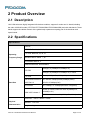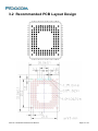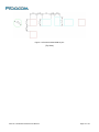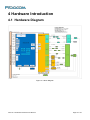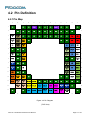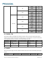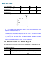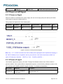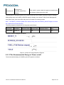
1
L810-GL LGA Module Hardware User Manual Version:V1.0.8 Date:2015.09.24 Copyright Copyright ©2015 Fibocom Wireless Inc . All rights reserved. Without the prior written permission of the copyright holder, any company or individual is prohibited to excerpt, copy any part of or the entire document, or transmit the document in any form. Attention The document is subject to update from time to time owing to the product version upgrade or other reasons. Unless otherwise specified, the document only serves as the user guide. All the statements, information and suggestions contained in the document do not constitute any explicit or implicit guarantee. Trademark The trademark is registered and owned by Fibocom Wireless Inc. Versions Version Date Remarks V1.0.0 2014-10-17 Initial Version V1.0.1 2014-11-24 Update the related specifications of bands 1.Change the definition of SIM2/ MMC(SDIO) pin to GND; V1.0.2 2014-12-15 2.Update the related circuit and description of SIM1_CD and POWER_ON/OFF. 1. Update the module appearance and power on/off timing diagram. 2. Modify the capacitance of SIM_DATA 3. Update the consumption, RF indicator and sensitivity 4. Modify the reset value of BODY_SAR and IPC_WAKEUP_HOST to V1.0.3 2015-02-06 PU. 5. Add the high-low range of voltage and the description of unused pin design. Modify the format : add a space behind of the “Band”, change the format of “LTE FDD”and “FDD LTE” to “LTE FDD”, change the format of L810-GL LGA Module Hardware User Manual Page 2 of 49 “TDD LTE” to “LTE TDD”,and simplify the hardware diagram. V1.0.4 2015-04-21 Add the description of “Bottom(Perspective)” in PCB Layout V1.0.5 2015-05-18 Update the translation of all the whole document . V1.0.6 2015-07-07 Update the title to “L810-GL Hardware User Manual” V1.0.7 2015-08-25 Update the logo. V1.0.8 2015-09-24 Change the data of Specifications Applicability Type No. Type 1 L810-GL-00 Note The difference of L810 LGA series wireless module as listed below: Model No. L810-GL-00 LTE FDD LTE TDD WCDMA TD-SCDMA Band Band Band Band 1, 3, 5, 7, 8, 20 38, 39, 40, 41 Ⅰ,Ⅷ A, F L810-GL LGA Module Hardware User Manual GSM/GPRS/EDGE 900/1800MHz Page 3 of 49 Content 1 Foreword.................................................................................................................................................................... 7 1.1 Introduction.....................................................................................................................................................7 1.2 Reference Standard......................................................................................................................................7 2 Product Overview..................................................................................................................................................... 9 2.1 Description......................................................................................................................................................9 2.2 Specifications................................................................................................................................................. 9 2.3 Appearance..................................................................................................................................................12 3 Structure...................................................................................................................................................................13 3.1 Dimension Diagram of Structure.............................................................................................................. 13 3.2 Recommended PCB Layout Design........................................................................................................14 4 Hardware Introduction........................................................................................................................................... 16 4.1 Hardware Diagram......................................................................................................................................16 4.2 Pin Definition................................................................................................................................................17 4.2.1 Pin Map............................................................................................................................................. 17 4.2.2 Description of Pins...........................................................................................................................18 5 Hardware Interface.................................................................................................................................................23 5.1 Power Interface........................................................................................................................................... 23 5.1.1 Power Supply................................................................................................................................... 23 5.1.2 Consumption.................................................................................................................................... 23 5.1.3 VSD2_1V8........................................................................................................................................ 26 5.1.4 VRTC................................................................................................................................................. 26 5.2 Power on/off and Reset Signal................................................................................................................. 27 5.2.1 Power on /off Signal........................................................................................................................ 28 5.2.1.1 Power on Signal................................................................................................................... 28 5.2.1.2 Power off signal.................................................................................................................... 28 5.2.1.3 The Recommended Design of Power on/off................................................................... 29 5.2.2 RESET Signal.................................................................................................................................. 30 5.3 Status Indicating Signal............................................................................................................................. 31 5.3.1 CORE DUMP Indicating................................................................................................................. 31 5.3.2 LPG Signal........................................................................................................................................31 5.3.3 WAKEUP_HOST............................................................................................................................. 32 5.3.4 PA_BLANKING Interface............................................................................................................... 32 L810-GL LGA Module Hardware User Manual Page 4 of 49 5.4 Interrupt Control Signal.............................................................................................................................. 32 5.4.1 WAKE_UP Signal............................................................................................................................ 33 5.4.2 W_DISABLE# Interface.................................................................................................................. 33 5.4.3 Android/Win8 Dual System Switch Control Interface................................................................ 33 5.4.4 BODY_SAR Interface..................................................................................................................... 34 5.5 USB Interface...............................................................................................................................................34 5.5.1 USB Interface Definition................................................................................................................. 34 5.5.2 USB Interface Application.............................................................................................................. 34 5.6 UART Interface............................................................................................................................................35 5.6.1 UART Interface Description........................................................................................................... 35 5.6.2 UART Interface Application............................................................................................................36 5.7 USIM Interface.............................................................................................................................................36 5.7.1 USIM Pins......................................................................................................................................... 36 5.7.2 USIM Interface Design....................................................................................................................37 5.7.2.1 “Normal Closed”SIM Card Circuit Design........................................................................ 37 5.7.2.2 “Normally Open” SIM Circuit Design.................................................................................37 5.7.3 Points for Attention in USIM Design............................................................................................. 38 5.7.4 USIM Hot-Plugging..........................................................................................................................38 5.7.4.1 Hardware Connection..........................................................................................................38 5.7.4.2 Software Settings................................................................................................................. 39 5.8 Digital Audio................................................................................................................................................. 39 5.8.1 I2S...................................................................................................................................................... 39 5.8.2 PCM Port Description..................................................................................................................... 40 5.9 I2C................................................................................................................................................................. 40 5.10 Clock Interface.......................................................................................................................................... 41 5.11 ADC Interface............................................................................................................................................ 41 5.12 Other Interfaces........................................................................................................................................ 41 6 Electrical and Environmental Features...............................................................................................................42 6.1 Electrical Features...................................................................................................................................... 42 6.2 Environmental Features.............................................................................................................................42 7 RF Interface.............................................................................................................................................................44 7.1 Operating Frequency Band....................................................................................................................... 44 7.2 TX Power...................................................................................................................................................... 44 7.3 Receiving Sensitivity...................................................................................................................................45 L810-GL LGA Module Hardware User Manual Page 5 of 49 7.4 RF PCB Design........................................................................................................................................... 47 7.4.1 Wiring Principle................................................................................................................................ 47 7.4.2 Impedance Design...........................................................................................................................47 7.5 Antenna Design........................................................................................................................................... 48 7.5.1 Main Antenna Design Requirements........................................................................................... 48 L810-GL LGA Module Hardware User Manual Page 6 of 49 1 Foreword 1.1 Introduction The document describes the electrical characteristics, RF performance, dimensions and application environment, etc. of L810 series wireless communication modules. With the assistance of the document and other instructions, developers can quickly understand the performance of L810 series wireless communication modules and develop products. 1.2 Reference Standard The design of the product compiles with the following standards : 3GPP TS 27.007 -v6.9.0: AT command set for User Equipment (UE) 3GPP TS 27.005 -v6.0.1: Use of Data Terminal Equipment -Data Circuit terminating Equipment (DTE-DCE) interface for Short Message Service (SMS) and Cell Broadcast Service (CBS) 3GPP TS 23.040 -v6.9.0: Technical realization of Short Message Service (SMS) 3GPP TS 24.011 -v6.1.0: Point- to - Point (PP) Short Message Service (SMS) support on mobile radio interface 3GPP TS 27.010 -v6.0.0: Terminal Equipment to User Equipment (TE-UE) multiplexer protocol 3GPP TS 3GPP TS 25.304-v6.10.0: User Equipment (UE) procedures in idle mode and procedures for cell 27.060 -v6.0.0: Packet domain; Mobile Station (MS) supporting Packet Switched services reselection in connected mode 3GPP TS 25.308 -v6.4.0: High Speed Downlink Packet Access (HSDPA); Overall description;Stage 2 3GPP TS 25.309 -v6.6.0: FDD enhanced uplink; Overall description; Stage 2 3GPP TS 23.038 -v6.1.0: Alphabets and language - specific information 3GPP TS 21.111 -v6.3.0: USIM and IC card requirements 3GPP TS 31.111 -v6.11.0 "USIM Application Toolkit (USAT)" 3GPP TS 45.002 -v6.12.0: Multiplexing and 3GPP TS 51.014 -v4.5.0: Specification of the SIM Application Toolkit for the Subscriber Identity multiple access on the radio path Module Mobile Equipment (SIM-ME) interface 3GPP TS 51.010 -1 -v6.7.0: Mobile Station (MS) conformance specification; Part 1: Conformance specification 3GPP TS 22.004 -v6.0.0: General on supplementary services L810-GL LGA Module Hardware User Manual Page 7 of 49 3GPP TS 23.090 -v6.1.0: Unstructured Supplementary Service Data (USSD); Stage 2 3GPP TS 24.008 v6.19, Mobile radio interface Layer 3 specification; 3GPP TS 25.101 V7.18.0: User Equipment (UE) radio transmission and reception (FDD) 3GPP TS 36.101V9.18.0: User Equipment (UE) radio transmission and reception 3GPP TS 36.104V9.13.0: Base Station (BS) radio transmission and reception 3GPP TS 36.106V9.4.0: FDD Repeater radio transmission and reception 3GPP TS 36.113V9.5.0: Base Station (BS) and repeater ElectroMagnetic Compatibility (EMC) 3GPP TS 36.124V9.2.0: ElectroMagnetic Compatibility (EMC) requirements for mobile terminals and ancillary equipment 3GPP TS 36.133V9.18.0:Requirements for support of radio resource management 3GPP TS 34.121-1 version 7.2.0: The requirements and this test apply to all types of UTRA for the FDD UE 3GPP TS 36.521-1 User Equipment (UE) conformance specification; Radio transmission and reception; Part 1: Conformance testing 3GPP TS 34.122V5.7.0: Technical Specification Group Radio Access Network; Radio transmission and reception (TDD) 3GPP TS 45.005 9.4.0: Digital cellular telecommunications system (Phase 2+);Radio transmission and reception L810-GL LGA Module Hardware User Manual Page 8 of 49 2 Product Overview 2.1 Description L810 LGA series are highly integrated 4G wireless modules, supports 5 modes and 11 bands,including the main 4G/3G/2G modes (LTE FDD/LTE TDD/WCDMA/TD-SCDMA/GSM) and with wide bands. These bands support the cellular network of the global major operators excepting part of the American and Japan bands. 2.2 Specifications Specifications L810-GL LTE FDD: Band 1, 3, 5, 7, 8, 20 Operating Frequency Range LTE TDD: Band 38, 39, 40, 41 WCDMA HSPA+: Band Ⅰ,Ⅷ TD-SCDMA: Band A, F GSM/GPRS/EDGE: 900/1800MHz Category 4 (150Mbps DL,50Mbps UL) LTE FDD Data Rare Category 6 (300Mbps DL,50Mbps UL) in future LTE TDD Cat 4 (112Mbps DL , 10Mbps UL ) UMTS/HSDPA/HSUPA DC-HSDPA 42Mbps(Cat24)/42Mbps(Cat20) 3GPP Rel.10 HSUPA 5.76Mbps(Cat7) TD-SCDMA DL 2.8Mbps, UL 2.2Mbps(Monolithic integration) EDGE (E-GPRS) multi-slot class 33(296kbps DL, GSM 3GPP release 7 236.8kbps UL) GPRS multi-slot class 33 (107kbps DL, 85.6kbps UL) Dimension:32mm x 26mm x 2.0mm Physical Interface:LGA 128 Characteristics Weight:4.0 grams L810-GL LGA Module Hardware User Manual Page 9 of 49 Operating Temperature:-30℃ ~ +75℃ Environment Storage Temperature:-40℃ ~ +85℃ Performance Operating Voltage Voltage: 3.3V ~ 4.4V Normal: 3.8V Sleep Mode: 5mA WCDMA/TD-SCDMA/LTE TDD Idle: 26mA LTE FDD Idle: 28mA Current Consumption (Typical Value) LTE FDD DATA: 650mA LTE TDD DATA: 380mA WCDMA Talk: 500mA TD-SCDMA Talk: 130mA 2G Talk: 260mA (GSM PCL5) Interfaces RF Interface Antenna:Mainx1,Diversityx1 1 x USB 2.0 1 x USB 3.0(not supported yet) 1 x UART MUX Over UART1 Multiple Profiles over USB Function Interface SIM Support I2C Support I2S Support JTAG/MIPI Trace HSIC/SSIC(not supported yet), EINT,System Indicator,A/D,Clock, RTC Data Features L810-GL LGA Module Hardware User Manual Page 10 of 49 Protocol Stack Embedded TCP/IP and UDP/IP protocol stack Multi-slot class 33 (5 Down; 4 Up; 6 Total) EDGE Coding Scheme MCS1~9 Multi-slot class 33 (5 Down; 4 Up; 6 Total) GPRS Coding SchemeMCS1~4 CSD UMTS(14.4kbps),GSM(9.6kbps) USSD Support SMS MO / MT Text and PDU modes Cell broadcast Digital Audio Audio Voice Coders: FR/HR/EFR/AMR-NB/AMR-WB VoLTE(not supported yet) Audio Control Gain Control , Echo Cancellation, Noise Suppression, EQ Modulation. Character Set IRA,GSM,UCS2,HEX FIBOCOM proprietary AT commands AT Commands GSM 07.05 GSM 07.07 Firmware Loader Tool over USB/UART Accessories User Manual Developer Kit L810-GL LGA Module Hardware User Manual Page 11 of 49 2.3 Appearance The product appearance of L810 series wireless module is shown as below: Top View: Figure 2- 1 Top View Bottom view: Figure 2- 2 Bottom View L810-GL LGA Module Hardware User Manual Page 12 of 49 3 Structure 3.1 Dimension Diagram of Structure Bot(Top View) Figure 3- 1 Dimension Diagram of Structure L810-GL LGA Module Hardware User Manual Page 13 of 49 3.2 Recommended PCB Layout Design L810-GL LGA Module Hardware User Manual Page 14 of 49 Figure 3- 2 Recommended PCB Layout (Top View) L810-GL LGA Module Hardware User Manual Page 15 of 49 4 Hardware Introduction 4.1 Hardware Diagram Figure 4- 1 Block Diagram L810-GL LGA Module Hardware User Manual Page 16 of 49 4.2 Pin Definition 4.2.1Pin Map A 1 B C D E F G H J K L GND GND ANT_DIV GND GND GND ANT_MAIN GND GND GND GND GND GND GND GND GND GND GND GND GND GND GND GND GND GND GND GND VBAT VBAT 3 GND GND VBAT VBAT 4 GND 2 M N GND 1 2 3 FSYS2_26 M RFE_RFFE 1_VIO GND GND 4 CORE_DUM P RFE_RFFE 1_SCLK IPC_HOST _WAKEUP GND 5 LPG RFE_RFFE 1_SDATA IPC_TRIG _OUT TDO TRST_N VRTC 5 6 GND GND GND HW_MON17 (TRC_DAT A0) TRIG_IN VSD2_1V8 6 7 WAKEUP_H OST GND IPC_TRIG _IN HW_MON18 (TRC_CLK ) TMS RESET_N 7 8 CLK32K GND IPC_SLAV E_WAKEUP GND GND PWR_ON/O FF# 8 9 UART1_TX D GND GND HW_MON19 (TRC_DAT A1) TCK I2S2_WA0 9 10 UART1_RX D GND ADC HW_MON20 (TRC_DAT A2) TDI I2S2_TX 10 11 VBUS GND GND HW_MON21 (TRC_DAT A3) I2C_SDA I2S2_RX 11 12 USB_DN USB_HSIC _STRB USB_HSIC _DATA GND GND GND I2C_SCL I2S2_CLK 12 13 USB_DP USB30_TX _DN USB30_TX _DP SSIC_RXP SSIC_RXN GND GND GND GND GND GND GND GND 13 USB30_RX _DN USB30_RX _DP SSIC_TXP SSIC_TXN SIM1_DP SIM1_DN EINT3 BODY_SAR UART1_RT S UART1_CT S GND GND VSIM1 SIM1_RST SIM1_CLK SIM1_DAT A SIM1_CD WAKEUP W_DISABL E# PA_BLANK ING/TRIG _OUT C D E F G H J K L 14 15 GND A B 14 GND M 15 N Figure 4-2 Pin Diagram (TOP View) L810-GL LGA Module Hardware User Manual Page 17 of 49 4.2.2Description of Pins The logic signal lever of L810 series is 1.8V Pins of L810 series are described in the table below: Pin# Pin Name I/O Reset Idle Value Value Description Power N3 VBAT PI Power input N4 VBAT PI Power input M3 VBAT PI Power input M4 VBAT PI Power input N5 VRTC PO VRTC output N6 VSD2_1V8 PO VSD2_1V8 output Power_ON/OFF#,RESET N7 RESET_N I Module reset input,pull up(100K ohms),1.8V N8 POWER_ON/OFF# I N9 I2S2_WA0 O PD T I2S LRCK,CMOS 1.8V N10 I2S2_TX O PD T I2S transmit data,CMOS 1.8V N11 I2S2_RX I PD T I2S receive data,CMOS 1.8V N12 I2S2_CLK O PD T I2S serial clock,CMOS 1.8V M11 I2C_SDA IO PU PU M12 I2C_SCL O PU PU A3 FSYS2_26M O A8 CLK32K O Module Power ON/OFF# signal,pull down (200K ohms),1.8V I2S I2C I2C serial data,pull up(4.7K ohms)CMOS 1.8V I2C serial clock,pull up(4.7K ohms)CMOS 1.8V Clock 26MHz clock output,1.8V PD PD 32kHz clock output,1.8V SIM1 D15 VSIM1 PO E15 SIM1_RST O L SIM1 reset F15 SIM1_CLK O L SIM1 clock G15 SIM1_DATA IO L SIM1 data,internal 4.7K resistor pull up L810-GL LGA Module Hardware User Manual SIM1 power supply,1.8V/2.8V Page 18 of 49 H15 SIM1_CD I T SIM1 detect, pull up(390K ohms)CMOS 1.8V F14 SIM1_DP IO PD USB data plus for SIM1 card G14 SIM1_DN IO PD USB data minus for SIM1 card USB2.0 A11 VBUS PI USB VBUS Supply A12 USB_DN IO T USB Data Minus A13 USB_DP IO T USB Data Plus USB3.0 C13 USB30_TX_DP IO USB3.0 Transmit data plus(not support now) B13 USB30_TX_DN IO C14 USB30_RX_DP IO USB3.0 receive data plus(not support now) B14 USB30_RX_DN IO USB3.0 receive data minus(not support now) B12 USB_HSIC_STRB IO High speed Inter IC clock(not support now) C12 USB_HSIC_DATA IO High speed Inter IC data(not support now) C4 IPC_HOST_WAKEUP O PU H IPC host wakeup(not support now) C5 IPC_TRIG_OUT O PD L IPC trig out(not support now) C7 IPC_TRIG_IN I PU PU I PD USB3.0 Transmit data minus(not support now) HSIC C8 IPC_SLAVE_WAKEU P IPC trig in(not support now) IPC slave wakeup(not support now) SSIC D14 SSIC_TXP IO SSIC transmit data plus(not support now) E14 SSIC_TXN IO SSIC transmit data minus(not support now) D13 SSIC_RXP IO SSIC receive data plus(not support now) E13 SSIC_RXN IO SSIC receive data minus(not support now) UART1 A9 UART1_TXD O PU PP UART1 transmit Data,CMOS 1.8V A10 UART1_RXD I PD PU UART1 receive Data,CMOS 1.8V K14 UART1_RTS O PU PP UART1 Request To Send,CMOS 1.8V L14 UART1_CTS I PU PU UART1 Clear To Send,CMOS 1.8V J15 WAKEUP I PD PU WAKEUP,CMOS 1.8V K15 W_DISABLE# I PD PU W_DISABLE#,CMOS 1.8V H14 EINT3 I PD PU EINT3,CMOS 1.8V EINT L810-GL LGA Module Hardware User Manual Page 19 of 49 J14 BODY_SAR I PU PU L BODY_SAR,CMOS 1.8V System status indicator A4 CORE_DUMP O PD A5 LPG O PD A7 WAKEUP_HOST O PU L O PD L L15 PA_BLANKING/ TRIG_OUT(T_OUT1) Core dump indicator,CMOS 1.8V LPG,CMOS 1.8V WAKEUP_HOST,CMOS 1.8V PA blanking output/Monitoring Signal Output,CMOS 1.8V ADC C10 ADC I General purpose A/D,1.2V max voltage L5 TDO O T M10 TDI I PU Serial Data Input M7 TMS I PU State machine control signal M9 TCK I PD JTAG clock input M5 TRST_N I PD Reset/Module enable M6 TRIG_IN I PD Monitoring Signal Input,CMOS 1.8V JTAG Serial Data Out MIPI2 Trace L7 MIPI2_TRC_CLK O PD PP MIPI2 trace clock,CMOS 1.8V L6 MIPI2_TRC_DATA0 IO PD PP MIPI2 trace data0,CMOS 1.8V L9 MIPI2_TRC_DATA1 IO PD PP MIPI2 trace data1,CMOS 1.8V L10 MIPI2_TRC_DATA2 IO PD PP MIPI2 trace data2,CMOS 1.8V L11 MIPI2_TRC_DATA3 IO PD PP MIPI2 trace data3,CMOS 1.8V ANT Tunable RFFE1 serial data for tunable ANT,CMOS B5 RFE_RFFE1_SDATA IO PP B4 RFE_RFFE1_SCLK O PP B3 RFE_RFFE1_VIO PO RFFE1 VIO for tunable ANT,1.8V J1 ANT_MAIN IO Main antenna E1 ANT_DIV B8 GND GND B9 GND GND B10 GND GND B11 GND GND 1.8V RFFE1 serial clock for tunable ANT,CMOS 1.8V ANT I L810-GL LGA Module Hardware User Manual Diversity antenna Page 20 of 49 C11 GND GND F13 GND GND L12 GND GND M13 GND GND L13 GND GND G13 GND GND H13 GND GND J13 GND GND K13 GND GND A6 GND GND B2 GND GND B6 GND GND B7 GND GND C1 GND GND C2 GND GND C3 GND GND C6 GND GND C9 GND GND C15 GND GND D1 GND GND D2 GND GND D3 GND GND D4 GND GND D12 GND GND E2 GND GND E3 GND GND F1 GND GND F2 GND GND F3 GND GND G1 GND GND G2 GND GND G3 GND GND H1 GND GND H2 GND GND H3 GND GND L810-GL LGA Module Hardware User Manual Page 21 of 49 J2 GND GND J3 GND GND K1 GND GND K2 GND GND K3 GND GND K4 GND GND K12 GND GND L1 GND GND L2 GND GND L3 GND GND L4 GND GND L8 GND GND M2 GND GND M8 GND GND M14 GND GND N13 GND GND A1 GND GND A15 GND GND N1 GND GND N15 GND GND H:High Voltage Level L:Low Voltage Level PD:Pull-Down PU:Pull-Up T:Tristate OD:Open Drain PP:Push-Pull Note : the unused pins can NC directly while designing. L810-GL LGA Module Hardware User Manual Page 22 of 49 5 Hardware Interface 5.1 Power Interface 5.1.1Power Supply L810 modules require 3.3V~4.5V direct current power supply, which can provide the maximum GSM emission current of 2A. Input power supply requirements: Parameter Minimum Value Recommended Value Maximum Value Unit VBAT 3.3 3.8 4.4 V Points for attention in design: 1. Supply voltage fluctuation shall be lower than 300mV. 2. Minimum supply voltage drop shall be higher than 3.1V. The filter capacitor design of power supply circuit as follows: Recommended Application capacitor 330uF Supply capacitance 1uF,100nF Digital signal noise 39pF,33pF 700 /850 /900 MHz 18pF,8.2pF,6.8pF Description Reduce power-supply fluctuation during phone call. The capacitance value bigger is better Filter the interference caused by clock and digital signals Filter RF interference 1700/1800/1900, 2100/2300,2500/2600MHz Filter RF interference 5.1.2Consumption Under the situation of 3.8V supply power , the consumption of L810 module as listed below : Parameter Ioff IIdle Description RTC mode Condition Current(mA) Power off 0.21 GSM MFRMS 5 25 WCDMA DRX 8 25 L810-GL LGA Module Hardware User Manual Page 23 of 49 TD-SCDMA 8 28 LTE FDD 8 27 LTE TDD 8 28 AT+cfun=4/1 24.5 2 3.5 5 2.9 9 2.6 6 3.5 8 2.7 9 2.6 8 3.2 8 4.9 8 4.6 AT+cfun=4/1 2.2 5 280 12 121 19 90 0 217 7 110 15 87 5 1829 12 473 19 207 0 1303 7 384 15 183 1 275 4 701 1 153 4 362 1 224 4 521 1 107 Radio Off RF is disabled. GSM ISleep MFRMS WCDMA DRX TD-SCDMA LTE FDD DRX LTE TDD Radio Off GSM voice RF is disabled. EGSM900 PCL IGSM-RMS RMS Current GSM voice DCS1800 PCL EGSM900 PCL IGSM-MAX Peak current DCS1800 PCL EGSM900 PCL=5(3) GPRS EGSM900 PCL=10(8) IGPRS-RMS CS4 1Rx slot nTX slot DCS1800 PCL=0(3) DCS1800 PCL=10(13) L810-GL LGA Module Hardware User Manual Page 24 of 49 EGSM900 PCL=8(6) EGPRS IEGPRS-RMS MCS9 EGSM900 PCL=15(13) 1Rx slot DCS1800 PCL=2(5) nTX slot DCS1800 PCL=10(13) Band 1 IWCDMA-RMS WCDMA Band 8 Band 34 ITD-SCDMA-RMS TD-SCDMA Band 39 B1 B3 ILTE-RMS LTE FDD B5 B7 L810-GL LGA Module Hardware User Manual 4 172 1 198 4 455 1 111 4 189 1 181 4 419 1 106 4 170 24dBm 667 10dBm 188 1dBm(0) 153 23.5dBm 588 10dBm 187 1dBm(0) 142 23dBm 128 10dBm 90 1dBm(0) 85 23dBm 129 10dBm 91 1dBm(0) 84 22dBm 576 10dBm 272 0dBm 224 21dBm 686 10dBm 281 0dBm 232 22.5dBm 649 10dBm 266 0dBm 221 22dBm 691 10dBm 285 0dBm 236 Page 25 of 49 22dBm 680 10dBm 275 0dBm 222 22.5dBm 654 10dBm 270 0dBm 219 23dBm 376 10dBm 200 0dBm 175 22.5dBm 298 10dBm 191 0dBm 171 22.5dBm 341 10dBm 199 0dBm 172 23dBm 368 10dBm 198 0dBm 176 B8 B20 B38 B39 LTE TDD B40 B41 5.1.3VSD2_1V8 As the power supply for the digital circuit inside the module, VSD2_1V8 can be used as the module`s reference level of the status index signal and digital signal. In circuit designing, only used for external low current application(<50mA). Of course , it can be kept floating if not used. Parameters Minimum Value Recommended Value Maximum Value Unit VSD2_1V8 1.7135 1.8 1.8865 V VIH 0.7* VSD2_1V8 1.8 1.8865 V VIL -0.3 0 0.3* VSD2_1V8 V 5.1.4VRTC VRTC is the power supply of the RTC inside the module, and it can be used as the backup power signal as well. Parameters Minimum Value L810-GL LGA Module Hardware User Manual Recommended Value Maximum Value Unit Page 26 of 49 VRTC output voltage VRTC input voltage 1.71 1.8 1.89 V 1.0 1.8 1.89 V 20 uA (RTC is in normal) VRTC input current (RTC is in normal) The reference design of VRTC circuit is as follows: Figure 5- 1 VRTC Reference Design Note: R8 is a current-limiting resistor, used to ensure the VRTC module works properly, free from being affected by peripheral circuits. R8≥1k ohm. VRTC power consumption current is about 10uA. The value of C9 will affect the retaining time of RTC after VBAT powers off. The retaining time of RTC can be roughly calculated by the following formula: T= (1.8-0.5)*C/1=1.3C, unit: second. Namely, if the value of C9 is 300uF, the retaining time of RTC will be around 30s. If the RTC backup power function is not required, VRTC pin can be floating. 5.2 Power on/off and Reset Signal L810 wireless communication modules provide two control signals to power on /power off and reset the modules. Pins definition as listed below : Pin# Pin Name Electrical Level Description Power off signal, power on with high N8 POWER_ON/OFF# CMOS 1.8V level, power off or floating with low level. L810-GL LGA Module Hardware User Manual Page 27 of 49 N7 RESET_N External reset signal input,active low. CMOS 1.8V 5.2.1Power on /off Signal 5.2.1.1Power on Signal After the module is connected to the power supply, the user can through pull up the start up the Power on/off signal to make the module power on. Timing sequence requirement of the startup pulse: Parameter Condition Minimum Value Typical Value Pulse Width Power on 20 100 Maximum Value Unit ms The timing sequence control is shown in the diagram below: Figure 5- 2 Power on Timing Control Diagram Note : the“>1s”of VBAT is the time aim at the module power supply(that is the capacitance charging). If the VBAT is already set up or supplied in the long term,then the control time that aimed at VBAT can ignore. AP-side only control the“ RESET_N”and “POWER_ON/OFF# “. 5.2.1.2Power off signal L810 module supports two power_off modes. Through the software modes to turn off the module in general condition. If the system halted or happened exceptions, use the following hardware modes to turn ① off it, pull down the POWER_ON/OFF# signal or floating . For details as listed below: Off modes Software off Methods Send AT+CPWROFF commands. L810-GL LGA Module Hardware User Manual Condition Normal power_off Page 28 of 49 Pull down the Hardware off POWER_ON/OFF# or floating. Only used for system halted or happens exceptions and the software modes cannot be used. The description of hardware power_off as follows (Pull down the POWER_ON/OFF# signal or floating) : While pulling down the POWER_ON/OFF# signal or floating, the modules` PMU (Power Management Unit) will be reset, then the module will get into off modes from working modes. ① Note : the RESET_N must be pulled down before pulling down the POWER_ON/OFF# signal, and then the module will be turned off safely. The timing sequence requirements of the pulse are as follows: Parameter Condition Minimum Value Typical Value Pulse Width Power off 5 100 Maximum Value Unit ms The timing sequence diagram as follows: Figure 5- 3 Power off Timing Sequence Diagram 5.2.1.3The Recommended Design of Power on/off The recommended design of POWER_ON/ OFF signal is as follows: L810-GL LGA Module Hardware User Manual Page 29 of 49 Figure 5- 4 Recommended Design of POWER_ON/OFF# Signal 5.2.2RESET Signal L810 wireless modules support external reset function. It is feasible to reset the module back to the original state by the Reset Signal. When setting the Reset Signal low for 100ms, the module will be reset and restarted. When the user uses the Reset_N function, the PMU inside the module will not lose power. Note: Reset signal is a sensitive signal line. In designing PCB layout, please keep the line away from RF interference, and make it well wrapped with ground wire. And it is advised to add an anti-shaking capacitor at the place close to the module end. At the same time, Reset_N signal line shall avoid the PCB edge and the surface, then reset the ESD can be avoided. The timing sequence requirements of its pulse are as follows: Parameter Condition Minimum Value Typical Value Maximum Value Unit Pulse Width Reset 7 100 1000 ms Recommended design: L810-GL LGA Module Hardware User Manual Page 30 of 49 Figure 5- 5 Recommended Design of Reset Circuit 5.3 Status Indicating Signal The pins of status indicating signal as listed below: Pin# Pin Name I/O Description A4 CORE_DUMP O Core Dump Indicator A5 LPG O LPG status Indicating A7 WAKEUP_HOST O The module wake-up Host(Application processor) L15 PA_BLANKING O PA Blanking output, external GPS control signal 5.3.1CORE DUMP Indicating Indicating for the module system is get into Core dump. Status Mode Normal mode Low level Core Dump High level 5.3.2LPG Signal LPG signal description as listed below : L810-GL LGA Module Hardware User Manual Page 31 of 49 Status Mode idle(unregistered) 600ms high level, 600ms low level idle(registered) 75ms high level, 3s low level Voice communication (Call) low level Data communicating 75ms high level, 75ms low level Sleep (sleep mode) high level 5.3.3WAKEUP_HOST The WAKEUP_HOST signal is for waking up the HOST while there are calls ,SMS or other data request. Status WAKEUP_HOST Signal Default High level Waking HOST (telephone ringing/SMS/other data request) Low level 5.3.4PA_BLANKING Interface The default output is low level .While the module works in GSM frequency band, PA_BLANKING will output the pulse signal that synchronize with the GSM Burst timing sequence. While the GSM TX may influence the GPS signal receiving, close GPS or stop receiving GPS data when AP detected the PA_BLANKING pulse signal. Operating modes PA_BLANKING Signal Default modes low level GSM TX output the pulse signal that synchronize with the GSM Burst 5.4 Interrupt Control Signal The pins of interrupt control signal as listed below: Pin# Name I/O Description J15 WAKEUP I AP wake up module K15 W_DISABLE# I Close or open RF network H14 EINT3 I Android/Win8 dual system switch L810-GL LGA Module Hardware User Manual Page 32 of 49 J14 BODY_SAR Body_SAR detection I 5.4.1WAKE_UP Signal WAKE_UP signal description as listed below : Module Mode Sleep Idle/Call WAKE_UP Signal Description Low level Wake up the module from Sleep mode to Idle mode High level Keep the module in Sleep mode Low level Keep the module in Idle/Call mode High level The module will not get into Sleep mode 5.4.2W_DISABLE# Interface The module provides hardware ways to open/close WWAN RF functional signal, for this function can be controlled by AT commands. The module will get into Fight modes while closing RF function. The definition of W_DISABLE# signal as list below: No. W_DISABLE# Function 1 Low WWAN closed, the module get into Flight modes. 2 High WWAN opened, the module exit Flight modes. 3 Floating The function of WWAN defined by AT commands , and keep open by default . 5.4.3Android/Win8 Dual System Switch Control Interface L810 module supports Win8/Android dual system switch, check and achieve the dual system switch through interrupt signal”EINT3”. The function definition of EINT3 signal as listed below: No. EINT3 Function 1 High/Floating Support Android system, the module`s `USB ports shall set as 3ACM modes. 2 Low Support Win8 system, the module`s USB ports shall set as MBIM modes. Description: 1. Check and achieve the Win8/Android system switch through GNSS_IRQ level when the module power on. Keep the GNSS_IRQ level stability during booting. 2. Check and achieve the Win8/Android system switch through GNSS_IRQ rising edge/ falling edge while the module power on, the de-bouncing time sets as 100ms. The module will reboot after meeting the requirements and can switch different system supports. L810-GL LGA Module Hardware User Manual Page 33 of 49 5.4.4BODY_SAR Interface L810 module supports BODY_SAR function. BODY_SAR is input signal (the signal is output directly by the AP or SAR SENSOR), the default is high level, and low level is effectively. While the human nearing, AP can detect it through the distance sensor, then output the BODY_SAR signal with low level. While the module detected the signal through the interruption, the module `s Tx power will be reduced and the threshold value can be set by the AT commands. Pin# Pin Name I/O Function Description J14 BODY_SAR I BODY_SAR Detection 5.5 USB Interface 5.5.1USB Interface Definition Pin# Pin Name I/O Description A13 USB_DP I/O USB signal+ A12 USB_DN I/O USB signal- A11 VBUS I USB power input L810 wireless communication modules support USB 2.0. Before connecting it to PC, it is necessary to install the related USB driver. After inserting the L810 wireless modules to PC, the USB interface will work with the driver and map three COM ports and four NCM ports on PC-side, as follows: Two COM ports for transmitting AT Command. One COM ports for capturing LOG information of the software. Four NCM ports are virtual network ports,mainly for initiating data traffic. Note: One of the COM port can use for Modem COM port and initiate data services. Due to the speed of Modem COM port is too slow to up to100Mbpss, the LTE downlink rate requirement,so it is not suggested. The Modem COM can be used to initiate data services temporarily only while the client`s NCM port is useless. 5.5.2USB Interface Application Reference Circuit Design: L810-GL LGA Module Hardware User Manual Page 34 of 49 Figure 5- 6 USB Interface Reference Circuit Design RV101 and RV102 shall be TVS with capacitance lower than 1pF; recommend to use the TVS with 0.5pF. There is no specific limitation for the capacitance of RV100 TVS. VUSB pin supplies power for USB. The recommended power supply range is 3.3V ~ 4.5V. In designing VUSB, there must be input, or it cannot recognize USB port. USB_DP and USB_DM are the high-speed differential signal line, and their highest transmission rate is 480Mbps. The following requirements should be followed in designing PCB layout. USB_DP and USB_DN signal lines should have the same length, and should be parallel; avoid right angle wiring; USB_DP and USB_DN signal lines should be wrapped with GND at the ends. USB2.0 differential signal line should be laid at the signal layer closest to the ground layer. Ensure impedance matching; impedance is required to be 90ohm. Note:VBUS shall detect power supply for module USB (belong to low current signal, current value<100uA). In circuit design, it shall not supply power to VBUS individually while the USB_DN and USB_DP disconnect, or the module will cannot get into sleep modes. 5.6 UART Interface 5.6.1UART Interface Description L810 wireless modules provide one 4-wire UART for the users; the UART1 supports AT commands, the users can receive and transmit AT commands through UART1. The definitions of UART1 signal interfaces are as follows: Pin# Pin Name I/O L810-GL LGA Module Hardware User Manual Description Page 35 of 49 L14 UART1_CTS I UART1 Clear to send K14 UART1_RTS O UART1 Request to send A9 UART1_TXD O UART1 Transmitted Data A10 UART1_RXD I UART1 Received Data 5.6.2UART Interface Application Connect UART1 of L810 wireless communication module (DCE) to PC, and the signal direction of (DTE) is as follows: MCU (DTE) application Signal direction L810 module (DCE) RXD UART1_TXD TXD UART1_RXD Note: the high level of the module’s UART interface is 1.8V. If it needs to connect it to 2.8V or 3.3V IO interface, it is necessary to switch the level. In design: it is recommended to use SN74LVC2G07 to switch the level from 1.8V to 3.3V. During the communication between UART1 and PC, firstly raise the level from 1.8V to 3.3V, and then, employSP3238 to switch the level. 5.7 USIM Interface L810 series wireless modules support USIM and high speed SIM cards. But 8-line intelligent USIM is not supported yet. 5.7.1USIM Pins Pin# Pin Name I/O Function Description D15 VSIM1 O USIM power supply signal ,1.8V/2.8V E15 SIM1_RST O USIM Reset Signal F15 SIM1_CLK O USIM clock signal G15 SIM1_DATA I/O USIM data signal USIM Plug-in detection signal , 390K resistor will be H15 SIM1_CD I pulled up by default. High level indicates that SIM card is inserted. Low level indicates that card is not inserted. L810-GL LGA Module Hardware User Manual Page 36 of 49 5.7.2USIM Interface Design 5.7.2.1“Normal Closed”SIM Card Circuit Design Reference Circuit Design:: Figure 5- 7 Reference Design of “Normally Closed” SIM Card Interface Normally closed SIM Connector: 1)Pull out SIM card, pin 7 and pin 8 will short-circuit . 2)Insert SIM card, pin 7 and pin 8 will disconnect. 5.7.2.2“Normally Open” SIM Circuit Design Referenced Circuit Design: Figure 5- 8 Reference Design of “Normally Closed” SIM Card Interface Normally closed SIM Connector: 1)Pull out SIM card, pin 7 and pin 8 short-circuit . 2)Insert SIM card, pin 7 and pin 8 disconnect. Note: L810-GL LGA Module Hardware User Manual Page 37 of 49 In order to improve EMC performance, the SIM card slot should be close to the module to the largest extent. The filter capacitor on the SIM-card signal circuit should be placed close to SIM card pin to the largest extent. ESD device (like TVS) shall be added to the SIM-card signal circuit protection. ESD device should be placed close to SIM card pin. SIM1_CD signal connection supports hot-plugging; active high level by default(change to active low through AT commands ). If the module detects the signal at high level, it means there is a card in the module. 5.7.3Points for Attention in USIM Design SIM card interface design is very important for the normal operation of the module and SIM card. The following points need to be complied with during the design: SIM card layout and wiring must keep away from EMI interference source, like RF antenna and digital switch signal. In order to ensure signal completeness, the wire distance between the module and SIM card should not exceed 100mm. In order to avoid mutual interference, USIM_CLK and USIM_IO signals should be separated in wiring. It would be best to wrap them with ground wire respectively. SIM card signal line should be protected with ESD. These protective devices should have small capacitance (like Zener diode, etc.). Users are recommended to select ESD devices with equivalent capacitance lower than 33pF. During layout, ESD device should be close to the SIM card interface. 5.7.4USIM Hot-Plugging L810 supports SIM card status-detection function. This function allows the hot-plugging of SIM card. 5.7.4.1Hardware Connection SIM card hot-plugging function needs to work with USIM_CD signal. USIM_CD will be at low level without SIM card; after inserting SIM card, USIM_CD will be at high level. Note: For “Normal closed” SIM card, as shown in the figure5-7, SIM1_CD signal line is connected to U2’s Pin8 (SW2), and Pin7 (SW1) is connected to the ground. When the SIM card is not inserted, SW2 and SW1 short circuit, SW2 will be at low level. When the SIM card is inserted, SW2 and SW1 will be disconnected, SIM1_CD level will be pulled up. For “Normal opened” SIM card, as shown in the figure5-8, SIM1_CD signal line is connected to U2’s L810-GL LGA Module Hardware User Manual Page 38 of 49 Pin8 (SW2), and Pin7 (SW1) will be pulled up 4.7K resistor . When the SIM card is not inserted, SW2 and SW1 will be disconnected, then SW2 will be at low level. When the SIM card is inserted, SW2 and SW1 will short circuit, SIM1_CD level will be pulled up. 5.7.4.2Software Settings “+MSMPD” configures AT command for the SIM card status-detection function. If set AT+MSMPD=0, SIM card status-detection function will be closed, and the module will not detect SIM1_CD signal. If set AT+MSMPD=1, SIM card status-detection function will be in operation, and the module will detect if the SIM card is inserted by SIM1_CD Pin. If SIM1_CD is at low level, which indicates SIM card is inserted, the module will automatically register it to the network. If SIM1_CD is at high level or unconnected, which indicates SIM card is not inserted, the module will not register it to the network. Note: the default of +MSMPD parameter is “1”.SIM_CD is the detection signal. While the module first power on or plug after that, SIM1_CD will detect if the SIM card is existing or not. Just only if the SIM1_CD is low level, the module will cannot read SIM card. 5.8 Digital Audio L810 supports digital audio I2S interface that supports normal I2S mode and PCM mode. I2S interface level is 1.8V on average. I2S signal description: Pin# Pin Name I/O Description N12 I2S2_CLK O Bit Clock,1.8V signal N9 I2S2_WA0 O Left and right channel clock (LRCK) ,1.8V signal N10 I2S2_TX O Serial data output ,1.8V signal N11 I2S2_RX I Serial data input ,1.8V signal 5.8.1I2S L810 Signal Direction Audio CODEC I2S Port I2S2_CLK0 I2S_CLK I2S2_WA0 I2S_LRCK L810-GL LGA Module Hardware User Manual Page 39 of 49 I2S2_RX I2S_SDOUT I2S2_TX I2S_SDIN Description: I2S interface can be configured as client-server work mode. Suitable for various audio sampling frequencies(48KHz, 44.1KHz, 32KHz, 24KHz, 22.5KHz, 16KHz, 12KHz, 11.025KHz and 8KHz). 5.8.2PCM Port Description L810 Signal Direction Audio CODEC PCM Port I2S2_CLK0(PCM_CLK ,PCM clock signal) PCM_CLK(PCM clock signal) I2S2_WA0(PCM_SYNC , PCM frame PCM_SYNC(PCM frame synchronization signal) synchronization signal) I2S2_RX(PCM_DIN , PCM data input) PCM_DOUT(PCM data output) I2S2_TX(PCM_DOUT , PCM data output) PCM_DIN(PCM data input) Note: PCM interface can be configured as client-server work mode. Support short frame synchronization at 16, 32, 48, and 64 bit mode Support burst and continuous mode transmission Supports clock length of frame synchronization signal and rising edge/ falling edge trigger configuration of data transmission. Suitable for various audio sampling frequencies(48KHz, 44.1KHz, 32KHz, 24KHz, 22.5KHz, 16KHz, 12KHz, 11.025KHz and 8KHz). Note: Cause the timing of I2S modes is easier than PCM modes and easier to fit, recommend clients to use transmission audio of I2S mode. While transmission with PCM modes, the PCM timing sequence is difficult to fit to make the tone quality become bad. 5.9 I2C L810 module supports one 12C interface, default configuration is I2C master. The I2C can use for driving external 12C slave device, such as Audio codes and so on. Pin# Name I/O Description M11 I2C_DATA I/O I2C control signal input/output ,1.8V signal M12 I2C_SCL O I2C control clock signal, 1.8V signal L810-GL LGA Module Hardware User Manual Page 40 of 49 The signal connection of L810 I2C and external 12C slave device ( such as Audio Codec)as listed below: L810 Signal Direction Audio Codec I2C Port I2C_SDA I2C_SDA I2C_SCL I2C_SCL 5.10 Clock Interface L810 module supports one 26MHz clock output and one 32KHz clock output. Pin# Pin Name I/O A3 FSYS2_26M O A8 CLK32K O Description 26Mclock output,1.8V (recommend used for external GPS, and can also used for main clock of audio codec) 32K clock output , 1.8V 5.11ADC Interface L810 supports ADC detection, with precision of 10bit. ADC input voltage is required to be 0~1.2V. ADC signal description: Pin# Pin Name I/O Description C10 ADC1 I ADC input 5.12 Other Interfaces The module does not support the following ports yet: USB3.0、HSIC、SSIC、SIM2、ANT Tunable、SDIO、 GPIO . L810-GL LGA Module Hardware User Manual Page 41 of 49 6 Electrical and Environmental Features 6.1 Electrical Features The table below lists the range of L810’s electrical characteristics: Parameters Minimum Value Maximum Value Unit Power supply signal 0 4.4 V Digital signal 0 1.9 V 6.2 Environmental Features This table below shows the environmental features of L810. Parameters Minimum Value L810-GL LGA Module Hardware User Manual Maximum Value Unit Page 42 of 49 Operational Temperature -30 +75 °C Storage Temperature -40 +85 °C L810-GL LGA Module Hardware User Manual Page 43 of 49 7 RF Interface 7.1 Operating Frequency Band The RF operating frequency band as listed below: Operating Band Description Mode Band 1 IMT 2100MHz LTE FDD/WCDMA 1920 - 1980 2110 - 2170 Band 3 DCS 1800MHz LTE FDD/GSM 1710 - 1785 1805 - 1880 Band 5 CLR 850MHz LTE FDD/WCDMA/GSM 824 - 849 869 - 894 Band 7 IMT-E 2600Mhz LTE FDD 2500 - 2570 2620 - 2690 Band 8 E-GSM 900MHz LTE FDD/WCDMA/GSM 880 - 915 925 - 960 Band 20 EUDD 800MHz LTE FDD 832 - 862 791 - 821 Band 34 IMT 2100MHz TDSCDMA 2010 - 2025 Band 38 IMT-E 2600MHz LTE TDD 2570 - 2620 Band 39 TDD 1900MHZ LTE TDD/TDSCDMA 1880 - 1920 Band 40 IMT 2300MHz LTE TDD 2300 - 2400 Band 41 BRS/EBS 2500MHZ LTE TDD 2496 - 2690 Tx (MHz) Rx (MHz) 7.2 TX Power For different modes , the TX power of L810 bands as listed below : Mode Band Tx Power(dBm) Note GSM 900 32.5 ±1dBm DCS 1800 29.5 ±1dBm Band 1 22.5 ±1dBm Band 8 22.5 ±1dBm Band 1 22.5 ±1dBm Band 3 22.5 ±1dBm GSM WCDMA LTE FDD L810-GL LGA Module Hardware User Manual Page 44 of 49 Band 5 22.5 ±1dBm Band 7 22.5 ±1dBm Band 8 22.5 ±1dBm Band 20 22.5 ±1dBm Band 38 22.5 ±1dBm Band 39 22.5 ±1dBm Band 40 22.5 ±1dBm Band 41 22.5 ±1dBm Band 34 22.5 ±1dBm Band 39 22.5 ±1dBm LTE TDD TD-SCDMA 7.3 Receiving Sensitivity For different modes , the receiving sensitivity of L810 bands as listed below : Mode Band Rx Sensitivity(dbm) Note GSM 900 -108 BER<2.43% DCS 1800 -108 BER<2.43% Band 1 -109 BER<0.1% Band 8 -109 BER<0.1% Band 1 -100 10MHz Band width Band 3 -101 10MHz Band width Band 5 -102 10MHz Band width Band 7 -99 10MHz Band width Band 8 -101.5 10MHz Band width Band 20 -101 10MHz Band width Band 38 -100 10MHz Band width Band 39 -100 10MHz Band width GSM WCDMA LTE FDD LTE TDD L810-GL LGA Module Hardware User Manual Page 45 of 49 Band 40 -99.5 10MHz Band width Band 41 -99.5 10MHz Band width Band 34 -109.5 BER<0.1% Band 39 -109.5 BER<0.1% TD-SCDMA Note : The above values are tested in the double antenna situation (Main+Diversity). If used the single antenna (without Diversity), the value of sensitivity will accordingly drop by some 3dbm. L810-GL LGA Module Hardware User Manual Page 46 of 49 7.4 RF PCB Design 7.4.1Wiring Principle L810 adopts double RF antennas, the MAIN_ANT used for transmitting and receiving, the DIV_ANT used for receiving. On the one hand, diversity antenna can improve the receiving sensitivity, on the other hand, it can also improve the download speed. Because the L810 project is for LTE module, the Antenna need double antennas can meet the performance requirements. Because L810 has no RF connector, the user needs to connect a length of RF line to the antenna, or design a connector on the board. So, it is recommended to use microstrip line for RF line. It should be as short as possible with loss controlled below 0.2dB, and impedance of 50 ohm. Reserve a π circuit (the earth terminals of the two parallel devices should be directly connected to the main ground) between L810 module and the antenna connector (or feed point) for antenna tuning. Figure 7- 1π-type Circuit 7.4.2Impedance Design The impedance of RF signal line of antenna interface needs to be controlled at 50 ohm. L810-GL LGA Module Hardware User Manual Page 47 of 49 7.5 Antenna Design 7.5.1Main Antenna Design Requirements (1) Antenna efficiency Antenna efficiency is the ratio of the input power and radiant power. Because of the antenna’s return loss, material loss and coupling loss, the radiant power is always lower than the input power. The ratio is recommended to be > 40% (–4dB). (2) S11 or VSWR S11 shows the matching degree of the antenna’s 50 ohm impedance, which affects antenna efficiency to a certain extent. It is feasible to use VSWR testing method to measure the index. It is recommended that S11 < –10dB. (3) Polarization Polarization is the rotation direction of the electric field of the antenna at the direction of the largest radiation. It is recommended to use linear polarization; for diversity antenna, it is recommended to use different polarization directions from that of the main antenna. (4) Radiation pattern Radiation pattern refers to the electromagnetic field intensity at various directions in the far field of the antenna. Half-wave doublet antenna is the perfect terminal antenna. In the case of built-in antenna, it is recommended to use PIFA. Antenna area: H 6mm * W 10mm * L 100mm. It is recommended to use PIFA or IFA. Antenna radiation direction: Omni-directional. (5) Gain and directivity Antenna directivity refers to the electromagnetic field intensity at various directions of the electromagnetic wave. Gain is the combination of the antenna efficiency and antenna directivity. It is recommended that antenna gain ≤ 2.5dBi. (6) Interference In addition to antenna performance, other interference from the PCB will also affect the module performance. In order to ensure the high performance of the module, the interference must be under control. Suggestions: keep speaker, LCD, CPU, FPC wiring, audio circuit, and power supply away from the antenna; add appropriate separation and shielding devices, or conduct filtering on the path. (7) TRP/TIS L810-GL LGA Module Hardware User Manual Page 48 of 49 TRP (Total Radiated Power): GSM900>28dBm GSM DCS1800 >25dBm WCDMA Band 1 ,8>19dBm TD-SCDMA Band 34,39>19dBm LTE FDD Band 1, 3, 5,7,8, 20>19dBm LTE TDD Band 38,39,40,41>19dBm TIS (Total Isotropic Sensitivity): GSM900,DCS1800<-102dBm WCDMA Band 1,8<-102dBm TD-SCDMA Band 34,39<-102dBm LTE FDD Band 1,3,5,7,8,20<-95dBm (10MHz Band width) LTE TDD Band 38,39,40,41<-95dBm (10MHz Band width) L810-GL LGA Module Hardware User Manual Page 49 of 49